Embed Size (px)
Citation preview

EFM8 Busy Bee FamilyEFM8BB1 Reference Manual
The EFM8BB1, part of the Busy Bee family of MCUs, is a multi-purpose line of 8-bit microcontrollers with a comprehensive featureset in small packages.These devices offer high-value by integrating advanced analog and communication pe-ripherals into small packages, making them ideal for space-constrained applications.With an efficient 8051 core, enhanced pulse-width modulation, and precision analog, theEFM8BB1 family is also optimal for embedded applications.
EFM8BB1 applications include the following:
KEY FEATURES
• Pipelined 8-bit C8051 core with 25 MHzmaximum operating frequency
• Up to 18 multifunction, 5 V tolerant I/O pins• One 12-bit Analog to Digital converter
(ADC)• Two low-current analog comparators• Integrated temperature sensor• 3-channel enhanced PWM / PCA• Four 16-bit timers• UART, SPI and SMBus/I2C• Priority crossbar for flexible pin mapping
• Motor control• Consumer electronics• Sensor controllers
• Medical equipment• Lighting systems• I/O port expander
SecurityI/O Ports
Core / Memory Clock Management
Low FrequencyRC Oscillator
Energy Management
Brown-Out Detector
8-bit SFR bus
Serial Interfaces Timers and Triggers Analog Interfaces
UART SPI
I2C / SMBus
External Interrupts
General Purpose I/O
Pin Reset 16-bit Timers PCA/PWM
Watchdog Timer
ADC Analog Comparators
Internal Voltage Reference
16-bit CRC
Flash Program Memory
(up to 8 KB)
RAM Memory(up to 512 bytes)
Lowest power mode with peripheral operational:
IdleNormal Shutdown
CIP-51 8051 Core(25 MHz)
Debug Interface with C2
External CMOS Oscillator
High FrequencyRC Oscillator
Internal LDO Regulator Power-On Reset
silabs.com | Smart. Connected. Energy-friendly. Rev. 0.2

1. System Overview
1.1 Introduction
Analog Peripherals
Digital Peripherals
CIP-51 8051 Controller Core
System Clock Configuration
AM
UX
Priority Crossbar Decoder
Crossbar Control
Port I/O Configuration
8/4/2 KB ISP FlashProgram Memory
256 Byte SRAM
SFR Bus
256 Byte XRAM
CRC
2 Comparators
Power NetVDD
GND
SYSCLK
CMOS Oscillator
Input
24.5 MHz 2%
Oscillator
Debug / Programming
Hardware
Power On Reset
Reset
C2D
C2CK/RSTb
12/10 bitADC
Temp Sensor
VREFVDD
VDD
EXTCLK
Low-Freq. Oscillator
Independent Watchdog Timer
Internal Reference
+-+-
UART
Timers 0, 1, 2, 3
3-ch PCA
I2C / SMBus
SPI
Port 0Drivers
Port 1 Drivers
P0.n
Port 2 Driver P2.n
P1.n
Figure 1.1. Detailed EFM8BB1 Block Diagram
EFM8BB1 Reference ManualSystem Overview
silabs.com | Smart. Connected. Energy-friendly. Rev. 0.2 | 1

1.2 Power
All internal circuitry draws power from the VDD supply pin. External I/O pins are powered from the VIO supply voltage (or VDD on devi-ces without a separate VIO connection), while most of the internal circuitry is supplied by an on-chip LDO regulator. Control over thedevice power can be achieved by enabling/disabling individual peripherals as needed. Each analog peripheral can be disabled whennot in use and placed in low power mode. Digital peripherals, such as timers and serial buses, have their clocks gated off and draw littlepower when they are not in use.
Table 1.1. Power Modes
Power Mode Details Mode Entry Wake-Up Sources
Normal Core and all peripherals clocked and fully operational — —
Idle • Core halted• All peripherals clocked and fully operational• Code resumes execution on wake event
Set IDLE bit in PCON0 Any interrupt
Shutdown • All internal power nets shut down• Pins retain state• Exit on pin or power-on reset
1. Set STOPCF bit inREG0CN
2. Set STOP bit inPCON0
• RSTb pin reset• Power-on reset
1.3 I/O
Digital and analog resources are externally available on the device’s multi-purpose I/O pins. Port pins P0.0-P1.7 can be defined as gen-eral-purpose I/O (GPIO), assigned to one of the internal digital resources through the crossbar or dedicated channels, or assigned to ananalog function. Port pins P2.0 and P2.1 can be used as GPIO. Additionally, the C2 Interface Data signal (C2D) is shared with P2.0.
• Up to 18 multi-functions I/O pins, supporting digital and analog functions.• Flexible priority crossbar decoder for digital peripheral assignment.• Two drive strength settings for each port.• Two direct-pin interrupt sources with dedicated interrupt vectors (INT0 and INT1).• Up to 16 direct-pin interrupt sources with shared interrupt vector (Port Match).
1.4 Clocking
The CPU core and peripheral subsystem may be clocked by both internal and external oscillator resources. By default, the systemclock comes up running from the 24.5 MHz oscillator divided by 8.
• Provides clock to core and peripherals.• 24.5 MHz internal oscillator (HFOSC0), accurate to ±2% over supply and temperature corners.• 80 kHz low-frequency oscillator (LFOSC0).• External CMOS clock input (EXTCLK).• Clock divider with eight settings for flexible clock scaling: Divide the selected clock source by 1, 2, 4, 8, 16, 32, 64, or 128.
EFM8BB1 Reference ManualSystem Overview
silabs.com | Smart. Connected. Energy-friendly. Rev. 0.2 | 2

1.5 Counters/Timers and PWM
Programmable Counter Array (PCA0)
The programmable counter array (PCA) provides multiple channels of enhanced timer and PWM functionality while requiring less CPUintervention than standard counter/timers. The PCA consists of a dedicated 16-bit counter/timer and one 16-bit capture/compare mod-ule for each channel. The counter/timer is driven by a programmable timebase that has flexible external and internal clocking options.Each capture/compare module may be configured to operate independently in one of five modes: Edge-Triggered Capture, SoftwareTimer, High-Speed Output, Frequency Output, or Pulse-Width Modulated (PWM) Output. Each capture/compare module has its ownassociated I/O line (CEXn) which is routed through the crossbar to port I/O when enabled.
• 16-bit time base• Programmable clock divisor and clock source selection• Up to three independently-configurable channels• 8, 9, 10, 11 and 16-bit PWM modes (center or edge-aligned operation)• Output polarity control• Frequency output mode• Capture on rising, falling or any edge• Compare function for arbitrary waveform generation• Software timer (internal compare) mode• Can accept hardware “kill” signal from comparator 0
Timers (Timer 0, Timer 1, Timer 2, and Timer 3)
Several counter/timers are included in the device: two are 16-bit counter/timers compatible with those found in the standard 8051, andthe rest are 16-bit auto-reload timers for timing peripherals or for general purpose use. These timers can be used to measure time inter-vals, count external events and generate periodic interrupt requests. Timer 0 and Timer 1 are nearly identical and have four primarymodes of operation. The other timers offer both 16-bit and split 8-bit timer functionality with auto-reload and capture capabilities.
Timer 0 and Timer 1 include the following features:• Standard 8051 timers, supporting backwards-compatibility with firmware and hardware.• Clock sources include SYSCLK, SYSCLK divided by 12, 4, or 48, the External Clock divided by 8, or an external pin.• 8-bit auto-reload counter/timer mode• 13-bit counter/timer mode• 16-bit counter/timer mode• Dual 8-bit counter/timer mode (Timer 0)
Timer 2 and Timer 3 are 16-bit timers including the following features:• Clock sources include SYSCLK, SYSCLK divided by 12, or the External Clock divided by 8.• 16-bit auto-reload timer mode• Dual 8-bit auto-reload timer mode• External pin capture (Timer 2)• LFOSC0 capture (Timer 3)
Watchdog Timer (WDT0)
The device includes a programmable watchdog timer (WDT) running off the low-frequency oscillator. A WDT overflow forces the MCUinto the reset state. To prevent the reset, the WDT must be restarted by application software before overflow. If the system experiencesa software or hardware malfunction preventing the software from restarting the WDT, the WDT overflows and causes a reset. Followinga reset, the WDT is automatically enabled and running with the default maximum time interval. If needed, the WDT can be disabled bysystem software or locked on to prevent accidental disabling. Once locked, the WDT cannot be disabled until the next system reset.The state of the RST pin is unaffected by this reset.
The Watchdog Timer has the following features:• Programmable timeout interval• Runs from the low-frequency oscillator• Lock-out feature to prevent any modification until a system reset
EFM8BB1 Reference ManualSystem Overview
silabs.com | Smart. Connected. Energy-friendly. Rev. 0.2 | 3

1.6 Communications and Other Digital Peripherals
Universal Asynchronous Receiver/Transmitter (UART0)
UART0 is an asynchronous, full duplex serial port offering modes 1 and 3 of the standard 8051 UART. Enhanced baud rate supportallows a wide range of clock sources to generate standard baud rates. Received data buffering allows UART0 to start reception of asecond incoming data byte before software has finished reading the previous data byte.
The UART module provides the following features:• Asynchronous transmissions and receptions• Baud rates up to SYSCLK/2 (transmit) or SYSCLK/8 (receive)• 8- or 9-bit data• Automatic start and stop generation
Serial Peripheral Interface (SPI0)
The serial peripheral interface (SPI) module provides access to a flexible, full-duplex synchronous serial bus. The SPI can operate as amaster or slave device in both 3-wire or 4-wire modes, and supports multiple masters and slaves on a single SPI bus. The slave-select(NSS) signal can be configured as an input to select the SPI in slave mode, or to disable master mode operation in a multi-masterenvironment, avoiding contention on the SPI bus when more than one master attempts simultaneous data transfers. NSS can also beconfigured as a firmware-controlled chip-select output in master mode, or disabled to reduce the number of pins required. Additionalgeneral purpose port I/O pins can be used to select multiple slave devices in master mode.
The SPI module includes the following features:• Supports 3- or 4-wire operation in master or slave modes.• Supports external clock frequencies up to SYSCLK / 2 in master mode and SYSCLK / 10 in slave mode.• Support for four clock phase and polarity options.• 8-bit dedicated clock clock rate generator.• Support for multiple masters on the same data lines.
System Management Bus / I2C (SMB0)
The SMBus I/O interface is a two-wire, bi-directional serial bus. The SMBus is compliant with the System Management Bus Specifica-tion, version 1.1, and compatible with the I2C serial bus.
The SMBus module includes the following features:• Standard (up to 100 kbps) and Fast (400 kbps) transfer speeds.• Support for master, slave, and multi-master modes.• Hardware synchronization and arbitration for multi-master mode.• Clock low extending (clock stretching) to interface with faster masters.• Hardware support for 7-bit slave and general call address recognition.• Firmware support for 10-bit slave address decoding.• Ability to inhibit all slave states.• Programmable data setup/hold times.
16-bit CRC (CRC0)
The cyclic redundancy check (CRC) module performs a CRC using a 16-bit polynomial. CRC0 accepts a stream of 8-bit data and poststhe 16-bit result to an internal register. In addition to using the CRC block for data manipulation, hardware can automatically CRC theflash contents of the device.
The CRC module is designed to provide hardware calculations for flash memory verification and communications protocols. The CRCmodule supports the standard CCITT-16 16-bit polynomial (0x1021), and includes the following features:• Support for CCITT-16 polynomial• Byte-level bit reversal• Automatic CRC of flash contents on one or more 256-byte blocks• Initial seed selection of 0x0000 or 0xFFFF
EFM8BB1 Reference ManualSystem Overview
silabs.com | Smart. Connected. Energy-friendly. Rev. 0.2 | 4

1.7 Analog
12-Bit Analog-to-Digital Converter (ADC0)
The ADC is a successive-approximation-register (SAR) ADC with 12-, 10-, and 8-bit modes, integrated track-and hold and a program-mable window detector. The ADC is fully configurable under software control via several registers. The ADC may be configured tomeasure different signals using the analog multiplexer. The voltage reference for the ADC is selectable between internal and externalreference sources.
• Up to 16 external inputs.• Single-ended 12-bit and 10-bit modes.• Supports an output update rate of 200 ksps samples per second in 12-bit mode or 800 ksps samples per second in 10-bit mode.• Operation in low power modes at lower conversion speeds.• Asynchronous hardware conversion trigger, selectable between software, external I/O and internal timer sources.• Output data window comparator allows automatic range checking.• Support for burst mode, which produces one set of accumulated data per conversion-start trigger with programmable power-on set-
tling and tracking time.• Conversion complete and window compare interrupts supported.• Flexible output data formatting.• Includes an internal fast-settling reference with two levels (1.65 V and 2.4 V) and support for external reference and signal ground.• Integrated temperature sensor.
Low Current Comparators (CMP0, CMP1)
Analog comparators are used to compare the voltage of two analog inputs, with a digital output indicating which input voltage is higher.External input connections to device I/O pins and internal connections are available through separate multiplexers on the positive andnegative inputs. Hysteresis, response time, and current consumption may be programmed to suit the specific needs of the application.
The comparator module includes the following features:• Up to 8 external positive inputs.• Up to 8 external negative inputs.• Additional input options:
• Internal connection to LDO output.• Direct connection to GND.
• Synchronous and asynchronous outputs can be routed to pins via crossbar.• Programmable hysteresis between 0 and ±20 mV• Programmable response time.• Interrupts generated on rising, falling, or both edges.
EFM8BB1 Reference ManualSystem Overview
silabs.com | Smart. Connected. Energy-friendly. Rev. 0.2 | 5
1.8 Reset Sources
Reset circuitry allows the controller to be easily placed in a predefined default condition. On entry to this reset state, the following occur:• The core halts program execution.• Module registers are initialized to their defined reset values unless the bits reset only with a power-on reset.• External port pins are forced to a known state.• Interrupts and timers are disabled.
All registers are reset to the predefined values noted in the register descriptions unless the bits only reset with a power-on reset. Thecontents of RAM are unaffected during a reset; any previously stored data is preserved as long as power is not lost. The Port I/O latch-es are reset to 1 in open-drain mode. Weak pullups are enabled during and after the reset. For Supply Monitor and power-on resets,the RSTb pin is driven low until the device exits the reset state. On exit from the reset state, the program counter (PC) is reset, and thesystem clock defaults to an internal oscillator. The Watchdog Timer is enabled, and program execution begins at location 0x0000.
Reset sources on the device include the following:• Power-on reset• External reset pin• Comparator reset• Software-triggered reset• Supply monitor reset (monitors VDD supply)• Watchdog timer reset• Missing clock detector reset• Flash error reset
1.9 Debugging
The EFM8BB1 devices include an on-chip Silicon Labs 2-Wire (C2) debug interface to allow flash programming and in-system debug-ging with the production part installed in the end application. The C2 interface uses a clock signal (C2CK) and a bi-directional C2 datasignal (C2D) to transfer information between the device and a host system. See the C2 Interface Specification for details on the C2protocol.
1.10 Bootloader
All devices come pre-programmed with a UART bootloader. This bootloader resides in flash and can be erased if it is not needed.
EFM8BB1 Reference ManualSystem Overview
silabs.com | Smart. Connected. Energy-friendly. Rev. 0.2 | 6

2. Memory Organization
2.1 Memory Organization
The memory organization of the CIP-51 System Controller is similar to that of a standard 8051. There are two separate memoryspaces: program memory and data memory. Program and data memory share the same address space but are accessed via differentinstruction types. Program memory consists of a non-volatile storage area that may be used for either program code or non-volatiledata storage. The data memory, consisting of "internal" and "external" data space, is implemented as RAM, and may be used only fordata storage. Program execution is not supported from the data memory space.
2.2 Program Memory
The CIP-51 core has a 64 KB program memory space. The product family implements some of this program memory space as in-sys-tem, re-programmable flash memory. Flash security is implemented by a user-programmable location in the flash block and providesread, write, and erase protection. All addresses not specified in the device memory map are reserved and may not be used for code ordata storage.
MOVX Instruction and Program Memory
The MOVX instruction in an 8051 device is typically used to access external data memory. On the devices, the MOVX instruction isnormally used to read and write on-chip XRAM, but can be re-configured to write and erase on-chip flash memory space. MOVC in-structions are always used to read flash memory, while MOVX write instructions are used to erase and write flash. This flash accessfeature provides a mechanism for the product to update program code and use the program memory space for non-volatile data stor-age.
2.3 Data Memory
The RAM space on the chip includes both an "internal" RAM area which is accessed with MOV instructions, and an on-chip "external"RAM area which is accessed using MOVX instructions. Total RAM varies, based on the specific device. The device memory map hasmore details about the specific amount of RAM available in each area for the different device variants.
Internal RAM
There are 256 bytes of internal RAM mapped into the data memory space from 0x00 through 0xFF. The lower 128 bytes of data memo-ry are used for general purpose registers and scratch pad memory. Either direct or indirect addressing may be used to access the lower128 bytes of data memory. Locations 0x00 through 0x1F are addressable as four banks of general purpose registers, each bank con-sisting of eight byte-wide registers. The next 16 bytes, locations 0x20 through 0x2F, may either be addressed as bytes or as 128 bitlocations accessible with the direct addressing mode.
The upper 128 bytes of data memory are accessible only by indirect addressing. This region occupies the same address space as theSpecial Function Registers (SFR) but is physically separate from the SFR space. The addressing mode used by an instruction whenaccessing locations above 0x7F determines whether the CPU accesses the upper 128 bytes of data memory space or the SFRs. In-structions that use direct addressing will access the SFR space. Instructions using indirect addressing above 0x7F access the upper128 bytes of data memory.
General Purpose Registers
The lower 32 bytes of data memory, locations 0x00 through 0x1F, may be addressed as four banks of general-purpose registers. Eachbank consists of eight byte-wide registers designated R0 through R7. Only one of these banks may be enabled at a time. Two bits inthe program status word (PSW) register, RS0 and RS1, select the active register bank. This allows fast context switching when enteringsubroutines and interrupt service routines. Indirect addressing modes use registers R0 and R1 as index registers.
EFM8BB1 Reference ManualMemory Organization
silabs.com | Smart. Connected. Energy-friendly. Rev. 0.2 | 7

Bit Addressable Locations
In addition to direct access to data memory organized as bytes, the sixteen data memory locations at 0x20 through 0x2F are also ac-cessible as 128 individually addressable bits. Each bit has a bit address from 0x00 to 0x7F. Bit 0 of the byte at 0x20 has bit address0x00 while bit 7 of the byte at 0x20 has bit address 0x07. Bit 7 of the byte at 0x2F has bit address 0x7F. A bit access is distinguishedfrom a full byte access by the type of instruction used (bit source or destination operands as opposed to a byte source or destination).
The MCS-51™ assembly language allows an alternate notation for bit addressing of the form XX.B where XX is the byte address and Bis the bit position within the byte. For example, the instruction:
Mov C, 22.3h
moves the Boolean value at 0x13 (bit 3 of the byte at location 0x22) into the Carry flag.
Stack
A programmer's stack can be located anywhere in the 256-byte data memory. The stack area is designated using the Stack Pointer(SP) SFR. The SP will point to the last location used. The next value pushed on the stack is placed at SP+1 and then SP is incremen-ted. A reset initializes the stack pointer to location 0x07. Therefore, the first value pushed on the stack is placed at location 0x08, whichis also the first register (R0) of register bank 1. Thus, if more than one register bank is to be used, the SP should be initialized to alocation in the data memory not being used for data storage. The stack depth can extend up to 256 bytes.
External RAM
On devices with more than 256 bytes of on-chip RAM, the additional RAM is mapped into the external data memory space (XRAM).Addresses in XRAM area accessed using the external move (MOVX) instructions.
Note: The 16-bit MOVX write instruction is also used for writing and erasing the flash memory. More details may be found in the flashmemory section.
EFM8BB1 Reference ManualMemory Organization
silabs.com | Smart. Connected. Energy-friendly. Rev. 0.2 | 8

2.4 Memory Map
8 KB Flash(16 x 512 Byte pages)
Security Page512 Bytes
0x1E00
0x1FFE0x1FFF Lock Byte
Reserved
0xFFFF
0x2000
0x0000
Figure 2.1. Flash Memory Map — 8 KB Devices
EFM8BB1 Reference ManualMemory Organization
silabs.com | Smart. Connected. Energy-friendly. Rev. 0.2 | 9

Reserved
4 KB Flash(8 x 512 Byte pages)
0x0E00
0xFFFF
0x0000
Security Page512 Bytes
Lock Byte
0x0FFE0x0FFF0x1000
Figure 2.2. Flash Memory Map — 4 KB Devices
EFM8BB1 Reference ManualMemory Organization
silabs.com | Smart. Connected. Energy-friendly. Rev. 0.2 | 10

Reserved
2 KB Flash(4 x 512 Byte pages)
0x0600
0xFFFF
0x0000
Security Page512 Bytes
Lock Byte
0x07FE0x07FF0x0800
Figure 2.3. Flash Memory Map — 2 KB Devices
Lower 128 Bytes RAM(Direct or Indirect Access)
0x000x1F
General-Purpose Register Banks
Bit-Addressable0x200x2F0x30
0x7F
Upper 128 Bytes RAM
(Indirect Access)
Special Function Registers
(Direct Access)
0x80
0xFF
On-Chip RAMAccessed with MOV Instructions as Indicated
Figure 2.4. Direct / Indirect RAM Memory
EFM8BB1 Reference ManualMemory Organization
silabs.com | Smart. Connected. Energy-friendly. Rev. 0.2 | 11

On-Chip XRAMAccessed with MOVX Instructions
XRAM256 Bytes
0x0000
0x00FF0x0100
Shadow XRAMDuplicates 0x0000-0x00FF
On 256 B boundaries
0xFFFF
Figure 2.5. XRAM Memory
EFM8BB1 Reference ManualMemory Organization
silabs.com | Smart. Connected. Energy-friendly. Rev. 0.2 | 12

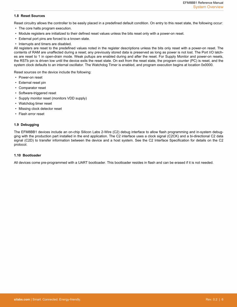
3. Special Function Registers
3.1 Special Function Register Access
The direct-access data memory locations from 0x80 to 0xFF constitute the special function registers (SFRs). The SFRs provide controland data exchange with the CIP-51's resources and peripherals. The CIP-51 duplicates the SFRs found in a typical 8051 implementa-tion as well as implementing additional SFRs used to configure and access the sub-systems unique to the MCU. This allows the addi-tion of new functionality while retaining compatibility with the MCS-51™ instruction set.
The SFR registers are accessed anytime the direct addressing mode is used to access memory locations from 0x80 to 0xFF. SFRswith addresses ending in 0x0 or 0x8 (e.g., P0, TCON, SCON0, IE, etc.) are bit-addressable as well as byte-addressable. All other SFRsare byte-addressable only. Unoccupied addresses in the SFR space are reserved for future use. Accessing these areas will have anindeterminate effect and should be avoided.
EFM8BB1 Reference ManualSpecial Function Registers
silabs.com | Smart. Connected. Energy-friendly. Rev. 0.2 | 13

3.2 Special Function Register Memory Map
Table 3.1. Special Function Registers by Address
Address Name Address Name Address Name Address Name
0x80* P0 0xA0* P2 0xC0* SMB0CN0 0xE0* ACC
0x81 SP 0xA1 SPI0CFG 0xC1 SMB0CF 0xE1 XBR0
0x82 DPL 0xA2 SPI0CKR 0xC2 SMB0DAT 0xE2 XBR1
0x83 DPH 0xA3 SPI0DAT 0xC3 ADC0GTL 0xE3 XBR2
0x84 - 0xA4 P0MDOUT 0xC4 ADC0GTH 0xE4 IT01CF
0x85 - 0xA5 P1MDOUT 0xC5 ADC0LTL 0xE5 -
0x86 - 0xA6 P2MDOUT 0xC6 ADC0LTH 0xE6 EIE1
0x87 PCON0 0xA7 - 0xC7 HFO0CAL 0xE7 -
0x88* TCON 0xA8* IE 0xC8* TMR2CN0 0xE8* ADC0CN0
0x89 TMOD 0xA9 CLKSEL 0xC9 REG0CN 0xE9 PCA0CPL1
0x8A TL0 0xAA CMP1MX 0xCA TMR2RLL 0xEA PCA0CPH1
0x8B TL1 0xAB CMP1MD 0xCB TMR2RLH 0xEB PCA0CPL2
0x8C TH0 0xAC SMB0TC 0xCC TMR2L 0xEC PCA0CPH2
0x8D TH1 0xAD DERIVID 0xCD TMR2H 0xED P1MAT
0x8E CKCON0 0xAE - 0xCE CRC0CN0 0xEE P1MASK
0x8F PSCTL 0xAF - 0xCF CRC0FLIP 0xEF RSTSRC
0x90* P1 0xB0* - 0xD0* PSW 0xF0* B
0x91 TMR3CN0 0xB1 LFO0CN 0xD1 REF0CN 0xF1 P0MDIN
0x92 TMR3RLL 0xB2 ADC0CN1 0xD2 CRC0AUTO 0xF2 P1MDIN
0x93 TMR3RLH 0xB3 ADC0AC 0xD3 CRC0CNT 0xF3 EIP1
0x94 TMR3L 0xB4 C2FPDAT 0xD4 P0SKIP 0xF4 -
0x95 TMR3H 0xB5 DEVICEID 0xD5 P1SKIP 0xF5 -
0x96 PCA0POL 0xB6 REVID 0xD6 SMB0ADM 0xF6 PRTDRV
0x97 WDTCN 0xB7 FLKEY 0xD7 SMB0ADR 0xF7 PCA0PWM
0x98* SCON0 0xB8* IP 0xD8* PCA0CN0 0xF8* SPI0CN0
0x99 SBUF0 0xB9 ADC0TK 0xD9 PCA0MD 0xF9 PCA0L
0x9A - 0xBA - 0xDA PCA0CPM0 0xFA PCA0H
0x9B CMP0CN0 0xBB ADC0MX 0xDB PCA0CPM1 0xFB PCA0CPL0
0x9C PCA0CLR 0xBC ADC0CF 0xDC PCA0CPM2 0xFC PCA0CPH0
0x9D CMP0MD 0xBD ADC0L 0xDD CRC0IN 0xFD P0MAT
0x9E PCA0CENT 0xBE ADC0H 0xDE CRC0DAT 0xFE P0MASK
EFM8BB1 Reference ManualSpecial Function Registers
silabs.com | Smart. Connected. Energy-friendly. Rev. 0.2 | 14

Address Name Address Name Address Name Address Name
0x9F CMP0MX 0xBF CMP1CN0 0xDF ADC0PWR 0xFF VDM0CN
Table 3.2. Special Function Registers by Name
Register Address Description
ACC 0xE0 Accumulator
ADC0AC 0xB3 ADC0 Accumulator Configuration
ADC0CF 0xBC ADC0 Configuration
ADC0CN0 0xE8 ADC0 Control 0
ADC0CN1 0xB2 ADC0 Control 1
ADC0GTH 0xC4 ADC0 Greater-Than High Byte
ADC0GTL 0xC3 ADC0 Greater-Than Low Byte
ADC0H 0xBE ADC0 Data Word High Byte
ADC0L 0xBD ADC0 Data Word Low Byte
ADC0LTH 0xC6 ADC0 Less-Than High Byte
ADC0LTL 0xC5 ADC0 Less-Than Low Byte
ADC0MX 0xBB ADC0 Multiplexer Selection
ADC0PWR 0xDF ADC0 Power Control
ADC0TK 0xB9 ADC0 Burst Mode Track Time
B 0xF0 B Register
CKCON0 0x8E Clock Control 0
CLKSEL 0xA9 Clock Select
CMP0CN0 0x9B Comparator 0 Control 0
CMP0MD 0x9D Comparator 0 Mode
CMP0MX 0x9F Comparator 0 Multiplexer Selection
CMP1CN0 0xBF Comparator 1 Control 0
CMP1MD 0xAB Comparator 1 Mode
CMP1MX 0xAA Comparator 1 Multiplexer Selection
CRC0AUTO 0xD2 CRC0 Automatic Control
CRC0CN0 0xCE CRC0 Control 0
CRC0CNT 0xD3 CRC0 Automatic Flash Sector Count
CRC0DAT 0xDE CRC0 Data Output
CRC0FLIP 0xCF CRC0 Bit Flip
CRC0IN 0xDD CRC0 Data Input
DERIVID 0xAD Derivative Identification
DEVICEID 0xB5 Device Identification
DPH 0x83 Data Pointer High
DPL 0x82 Data Pointer Low
EFM8BB1 Reference ManualSpecial Function Registers
silabs.com | Smart. Connected. Energy-friendly. Rev. 0.2 | 15
Register Address Description
EIE1 0xE6 Extended Interrupt Enable 1
EIP1 0xF3 Extended Interrupt Priority 1
FLKEY 0xB7 Flash Lock and Key
HFO0CAL 0xC7 High Frequency Oscillator 0 Calibration
IE 0xA8 Interrupt Enable
IP 0xB8 Interrupt Priority
IT01CF 0xE4 INT0/INT1 Configuration
LFO0CN 0xB1 Low Frequency Oscillator Control
P0 0x80 Port 0 Pin Latch
P0MASK 0xFE Port 0 Mask
P0MAT 0xFD Port 0 Match
P0MDIN 0xF1 Port 0 Input Mode
P0MDOUT 0xA4 Port 0 Output Mode
P0SKIP 0xD4 Port 0 Skip
P1 0x90 Port 1 Pin Latch
P1MASK 0xEE Port 1 Mask
P1MAT 0xED Port 1 Match
P1MDIN 0xF2 Port 1 Input Mode
P1MDOUT 0xA5 Port 1 Output Mode
P1SKIP 0xD5 Port 1 Skip
P2 0xA0 Port 2 Pin Latch
P2MDOUT 0xA6 Port 2 Output Mode
PCA0CENT 0x9E PCA Center Alignment Enable
PCA0CLR 0x9C PCA Comparator Clear Control
PCA0CN0 0xD8 PCA Control
PCA0CPH0 0xFC PCA Channel 0 Capture Module High Byte
PCA0CPH1 0xEA PCA Channel 1 Capture Module High Byte
PCA0CPH2 0xEC PCA Channel 2 Capture Module High Byte
PCA0CPL0 0xFB PCA Channel 0 Capture Module Low Byte
PCA0CPL1 0xE9 PCA Channel 1 Capture Module Low Byte
PCA0CPL2 0xEB PCA Channel 2 Capture Module Low Byte
PCA0CPM0 0xDA PCA Channel 0 Capture/Compare Mode
PCA0CPM1 0xDB PCA Channel 1 Capture/Compare Mode
PCA0CPM2 0xDC PCA Channel 2 Capture/Compare Mode
PCA0H 0xFA PCA Counter/Timer High Byte
PCA0L 0xF9 PCA Counter/Timer Low Byte
PCA0MD 0xD9 PCA Mode
EFM8BB1 Reference ManualSpecial Function Registers
silabs.com | Smart. Connected. Energy-friendly. Rev. 0.2 | 16

Register Address Description
PCA0POL 0x96 PCA Output Polarity
PCA0PWM 0xF7 PCA PWM Configuration
PCON0 0x87 Power Control
PRTDRV 0xF6 Port Drive Strength
PSCTL 0x8F Program Store Control
PSW 0xD0 Program Status Word
REF0CN 0xD1 Voltage Reference Control
REG0CN 0xC9 Voltage Regulator 0 Control
REVID 0xB6 Revision Identifcation
RSTSRC 0xEF Reset Source
SBUF0 0x99 UART0 Serial Port Data Buffer
SCON0 0x98 UART0 Serial Port Control
SMB0ADM 0xD6 SMBus 0 Slave Address Mask
SMB0ADR 0xD7 SMBus 0 Slave Address
SMB0CF 0xC1 SMBus 0 Configuration
SMB0CN0 0xC0 SMBus 0 Control
SMB0DAT 0xC2 SMBus 0 Data
SMB0TC 0xAC SMBus 0 Timing and Pin Control
SP 0x81 Stack Pointer
SPI0CFG 0xA1 SPI0 Configuration
SPI0CKR 0xA2 SPI0 Clock Rate
SPI0CN0 0xF8 SPI0 Control
SPI0DAT 0xA3 SPI0 Data
TCON 0x88 Timer 0/1 Control
TH0 0x8C Timer 0 High Byte
TH1 0x8D Timer 1 High Byte
TL0 0x8A Timer 0 Low Byte
TL1 0x8B Timer 1 Low Byte
TMOD 0x89 Timer 0/1 Mode
TMR2CN0 0xC8 Timer 2 Control 0
TMR2H 0xCD Timer 2 High Byte
TMR2L 0xCC Timer 2 Low Byte
TMR2RLH 0xCB Timer 2 Reload High Byte
TMR2RLL 0xCA Timer 2 Reload Low Byte
TMR3CN0 0x91 Timer 3 Control 0
TMR3H 0x95 Timer 3 High Byte
TMR3L 0x94 Timer 3 Low Byte
EFM8BB1 Reference ManualSpecial Function Registers
silabs.com | Smart. Connected. Energy-friendly. Rev. 0.2 | 17

Register Address Description
TMR3RLH 0x93 Timer 3 Reload High Byte
TMR3RLL 0x92 Timer 3 Reload Low Byte
VDM0CN 0xFF Supply Monitor Control
WDTCN 0x97 Watchdog Timer Control
XBR0 0xE1 Port I/O Crossbar 0
XBR1 0xE2 Port I/O Crossbar 1
XBR2 0xE3 Port I/O Crossbar 2
EFM8BB1 Reference ManualSpecial Function Registers
silabs.com | Smart. Connected. Energy-friendly. Rev. 0.2 | 18

4. Flash Memory
4.1 Introduction
On-chip, re-programmable flash memory is included for program code and non-volatile data storage. The flash memory is organized in512-byte pages. It can be erased and written through the C2 interface or from firmware by overloading the MOVX instruction. Any indi-vidual byte in flash memory must only be written once between page erase operations.
8 KB Flash(16 x 512 Byte pages)
Security Page512 Bytes
0x1E00
0x1FFE0x1FFF Lock Byte
Reserved
0xFFFF
0x2000
0x0000
Figure 4.1. Flash Memory Map — 8 KB Devices
EFM8BB1 Reference ManualFlash Memory
silabs.com | Smart. Connected. Energy-friendly. Rev. 0.2 | 19

Reserved
4 KB Flash(8 x 512 Byte pages)
0x0E00
0xFFFF
0x0000
Security Page512 Bytes
Lock Byte
0x0FFE0x0FFF0x1000
Figure 4.2. Flash Memory Map — 4 KB Devices
EFM8BB1 Reference ManualFlash Memory
silabs.com | Smart. Connected. Energy-friendly. Rev. 0.2 | 20

Reserved
2 KB Flash(4 x 512 Byte pages)
0x0600
0xFFFF
0x0000
Security Page512 Bytes
Lock Byte
0x07FE0x07FF0x0800
Figure 4.3. Flash Memory Map — 2 KB Devices
4.2 Features
The flash memory has the following features:• Up to 8 KB organized in 512-byte sectors.• In-system programmable from user firmware.• Security lock to prevent unwanted read/write/erase access.
EFM8BB1 Reference ManualFlash Memory
silabs.com | Smart. Connected. Energy-friendly. Rev. 0.2 | 21

4.3 Functional Description
4.3.1 Security Options
The CIP-51 provides security options to protect the flash memory from inadvertent modification by software as well as to prevent theviewing of proprietary program code and constants. The Program Store Write Enable (bit PSWE in register PSCTL) and the ProgramStore Erase Enable (bit PSEE in register PSCTL) bits protect the flash memory from accidental modification by software. PSWE mustbe explicitly set to 1 before software can modify the flash memory; both PSWE and PSEE must be set to 1 before software can eraseflash memory. Additional security features prevent proprietary program code and data constants from being read or altered across theC2 interface.
A Security Lock Byte located in flash user space offers protection of the flash program memory from access (reads, writes, or erases)by unprotected code or the C2 interface. See the specific device memory map for the location of the security byte. The flash securitymechanism allows the user to lock "n" flash pages, starting at page 0, where "n" is the 1s complement number represented by theSecurity Lock Byte.Note: The page containing the flash Security Lock Byte is unlocked when no other flash pages are locked (all bits of the Lock Byte are1) and locked when any other flash pages are locked (any bit of the Lock Byte is 0).
Table 4.1. Security Byte Decoding
Security Lock Byte 111111101b
1s Complement 00000010b
Flash Pages Locked 3 (First two flash pages + Lock Byte Page)
The level of flash security depends on the flash access method. The three flash access methods that can be restricted are reads,writes, and erases from the C2 debug interface, user firmware executing on unlocked pages, and user firmware executing on lockedpages.
Table 4.2. Flash Security Summary—Firmware Permissions
Permissions according to the area firmware is executing from:
Target Area for Read / Write / Erase Unlocked UserPage
Locked User Page Unlocked DataPage
Locked Data Page
Any Unlocked Page [R] [W] [E] [R] [W] [E] [R] [W] [E] [R] [W] [E]
Locked Page (except security page) reset [R] [W] [E] reset [R] [W] [E]
Locked Security Page reset [R] [W] reset [R] [W]
Reserved Area reset reset reset reset
[R] = Read permitted
[W] = Write permitted
[E] = Erase permitted
reset = Flash error reset triggered
n/a = Not applicable
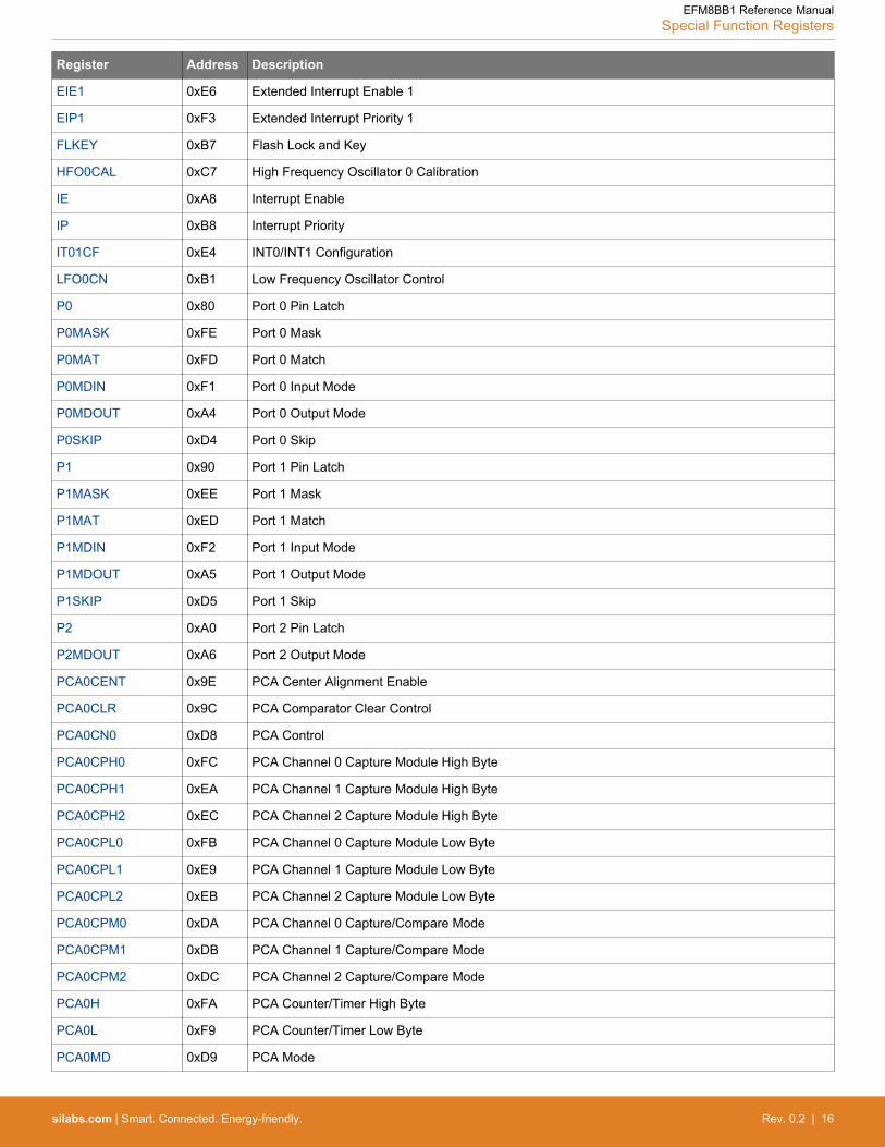
Table 4.3. Flash Security Summary—C2 Permissions
Target Area for Read / Write / Erase Permissions from C2 interface
Any Unlocked Page [R] [W] [E]
Any Locked Page Device Erase Only
Reserved Area None
EFM8BB1 Reference ManualFlash Memory
silabs.com | Smart. Connected. Energy-friendly. Rev. 0.2 | 22
Target Area for Read / Write / Erase Permissions from C2 interface
[R] = Read permitted
[W] = Write permitted
[E] = Erase permitted
Device Erase Only = No read, write, or individual page erase is allowed. Must erase entire flash space.
None = Read, write and erase are not permitted
4.3.2 Programming the Flash Memory
Writes to flash memory clear bits from logic 1 to logic 0 and can be performed on single byte locations. Flash erasures set bits back tologic 1 and occur only on full pages. The write and erase operations are automatically timed by hardware for proper execution; datapolling to determine the end of the write/erase operation is not required. Code execution is stalled during a flash write/erase operation.
The simplest means of programming the flash memory is through the C2 interface using programming tools provided by Silicon Labs ora third party vendor. Firmware may also be loaded into the device to implement code-loader functions or allow non-volatile data stor-age. To ensure the integrity of flash contents, it is strongly recommended that the on-chip supply monitor be enabled in any system thatincludes code that writes and/or erases flash memory from software.
4.3.2.1 Flash Lock and Key Functions
Flash writes and erases by user software are protected with a lock and key function. The FLKEY register must be written with the cor-rect key codes, in sequence, before flash operations may be performed. The key codes are 0xA5 and 0xF1. The timing does not mat-ter, but the codes must be written in order. If the key codes are written out of order or the wrong codes are written, flash writes anderases will be disabled until the next system reset. Flash writes and erases will also be disabled if a flash write or erase is attemptedbefore the key codes have been written properly. The flash lock resets after each write or erase; the key codes must be written againbefore another flash write or erase operation can be performed.
4.3.2.2 Flash Page Erase Procedure
The flash memory is erased one page at a time by firmware using the MOVX write instruction with the address targeted to any bytewithin the page. Before erasing a page of flash memory, flash write and erase operations must be enabled by setting the PSWE andPSEE bits in the PSCTL register to logic 1 (this directs the MOVX writes to target flash memory and enables page erasure) and writingthe flash key codes in sequence to the FLKEY register. The PSWE and PSEE bits remain set until cleared by firmware.
Erase operation applies to an entire page (setting all bytes in the page to 0xFF). To erase an entire page, perform the following steps:1. Disable interrupts (recommended).2. Write the first key code to FLKEY: 0xA5.3. Write the second key code to FLKEY: 0xF1.4. Set the PSEE bit (register PSCTL).5. Set the PSWE bit (register PSCTL).6. Using the MOVX instruction, write a data byte to any location within the page to be erased.7. Clear the PSWE and PSEE bits.
4.3.2.3 Flash Byte Write Procedure
The flash memory is written by firmware using the MOVX write instruction with the address and data byte to be programmed providedas normal operands in DPTR and A. Before writing to flash memory using MOVX, flash write operations must be enabled by setting thePSWE bit in the PSCTL register to logic 1 (this directs the MOVX writes to target flash memory) and writing the flash key codes insequence to the FLKEY register. The PSWE bit remains set until cleared by firmware. A write to flash memory can clear bits to logic 0but cannot set them. A byte location to be programmed should be erased (already set to 0xFF) before a new value is written.
To write a byte of flash, perform the following steps:1. Disable interrupts (recommended).2. Write the first key code to FLKEY: 0xA5.3. Write the second key code to FLKEY: 0xF1.4. Set the PSWE bit (register PSCTL).5. Clear the PSEE bit (register PSCTL).6. Using the MOVX instruction, write a single data byte to the desired location within the desired page.
EFM8BB1 Reference ManualFlash Memory
silabs.com | Smart. Connected. Energy-friendly. Rev. 0.2 | 23

7. Clear the PSWE bit.
4.3.3 Flash Write and Erase Precautions
Any system which contains routines which write or erase flash memory from software involves some risk that the write or erase routineswill execute unintentionally if the CPU is operating outside its specified operating range of supply voltage, system clock frequency ortemperature. This accidental execution of flash modifying code can result in alteration of flash memory contents causing a system fail-ure that is only recoverable by re-flashing the code in the device.
To help prevent the accidental modification of flash by firmware, hardware restricts flash writes and erasures when the supply monitor isnot active and selected as a reset source. As the monitor is enabled and selected as a reset source by default, it is recommended thatsystems writing or erasing flash simply maintain the default state.
The following sections provide general guidelines for any system which contains routines which write or erase flash from code. Addi-tional flash recommendations and example code can be found in AN201: Writing to Flash From Firmware, available from the SiliconLaboratories website.
Voltage Supply Maintenance and the Supply Monitor
• If the system power supply is subject to voltage or current "spikes," add sufficient transient protection devices to the power supply toensure that the supply voltages listed in the Absolute Maximum Ratings table are not exceeded.
• Make certain that the minimum supply rise time specification is met. If the system cannot meet this rise time specification, then addan external supply brownout circuit to the RSTb pin of the device that holds the device in reset until the voltage supply reaches thelower limit, and re-asserts RSTb if the supply drops below the low supply limit.
• Do not disable the supply monitor. If the supply monitor must be disabled in the system, firmware should be added to the startuproutine to enable the on-chip supply monitor and enable the supply monitor as a reset source as early in code as possible. Thisshould be the first set of instructions executed after the reset vector. For C-based systems, this may involve modifying the startupcode added by the C compiler. See your compiler documentation for more details. Make certain that there are no delays in softwarebetween enabling the supply monitor and enabling the supply monitor as a reset source.Note: The supply monitor must be enabled and enabled as a reset source when writing or erasing flash memory. A flash error resetwill occur if either condition is not met.
• As an added precaution if the supply monitor is ever disabled, explicitly enable the supply monitor and enable the supply monitor asa reset source inside the functions that write and erase flash memory. The supply monitor enable instructions should be placed justafter the instruction to set PSWE to a 1, but before the flash write or erase operation instruction.
• Make certain that all writes to the RSTSRC (Reset Sources) register use direct assignment operators and explicitly do not use thebit-wise operators (such as AND or OR). For example, "RSTSRC = 0x02" is correct. "RSTSRC |= 0x02" is incorrect.
• Make certain that all writes to the RSTSRC register explicitly set the PORSF bit to a 1. Areas to check are initialization code whichenables other reset sources, such as the Missing Clock Detector or Comparator, for example, and instructions which force a Soft-ware Reset. A global search on "RSTSRC" can quickly verify this.
PSWE Maintenance
• Reduce the number of places in code where the PSWE bit (in register PSCTL) is set to a 1. There should be exactly one routine incode that sets PSWE to a 1 to write flash bytes and one routine in code that sets PSWE and PSEE both to a 1 to erase flash pages.
• Minimize the number of variable accesses while PSWE is set to a 1. Handle pointer address updates and loop variable maintenanceoutside the "PSWE = 1;... PSWE = 0;" area.
• Disable interrupts prior to setting PSWE to a 1 and leave them disabled until after PSWE has been reset to 0. Any interrupts postedduring the flash write or erase operation will be serviced in priority order after the flash operation has been completed and interruptshave been re-enabled by software.
• Make certain that the flash write and erase pointer variables are not located in XRAM. See your compiler documentation for instruc-tions regarding how to explicitly locate variables in different memory areas.
• Add address bounds checking to the routines that write or erase flash memory to ensure that a routine called with an illegal addressdoes not result in modification of the flash.
System Clock
• If operating from an external crystal-based source, be advised that crystal performance is susceptible to electrical interference and issensitive to layout and to changes in temperature. If the system is operating in an electrically noisy environment, use the internaloscillator or use an external CMOS clock.
• If operating from the external oscillator, switch to the internal oscillator during flash write or erase operations. The external oscillatorcan continue to run, and the CPU can switch back to the external oscillator after the flash operation has completed.
EFM8BB1 Reference ManualFlash Memory
silabs.com | Smart. Connected. Energy-friendly. Rev. 0.2 | 24
4.4 Flash Control Registers
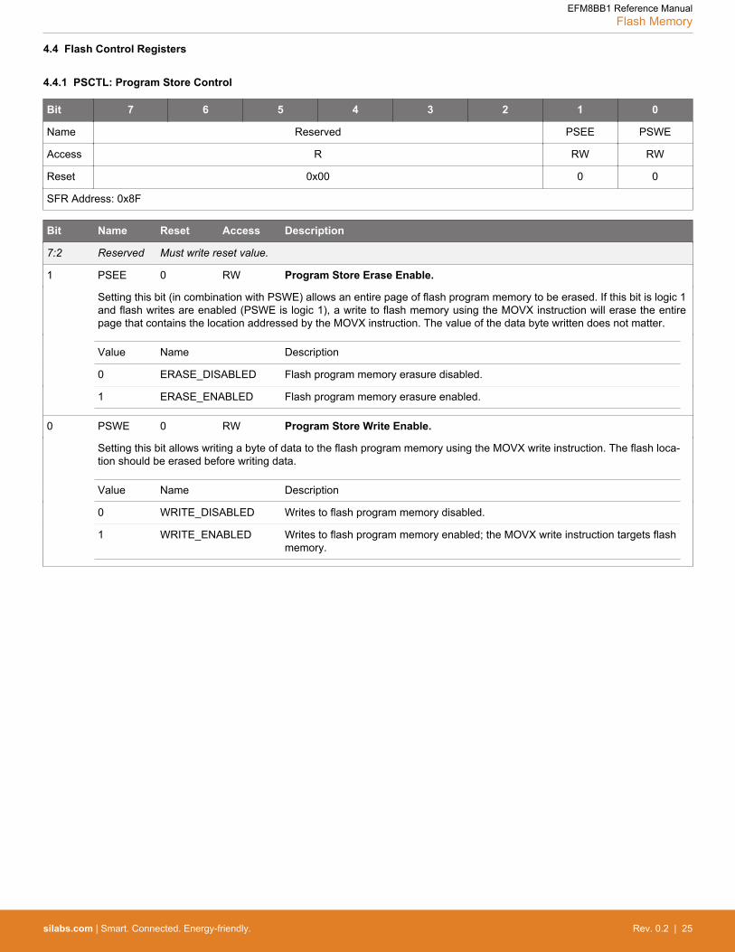
4.4.1 PSCTL: Program Store Control
Bit 7 6 5 4 3 2 1 0
Name Reserved PSEE PSWE
Access R RW RW
Reset 0x00 0 0
SFR Address: 0x8F
Bit Name Reset Access Description
7:2 Reserved Must write reset value.
1 PSEE 0 RW Program Store Erase Enable.
Setting this bit (in combination with PSWE) allows an entire page of flash program memory to be erased. If this bit is logic 1and flash writes are enabled (PSWE is logic 1), a write to flash memory using the MOVX instruction will erase the entirepage that contains the location addressed by the MOVX instruction. The value of the data byte written does not matter.
Value Name Description
0 ERASE_DISABLED Flash program memory erasure disabled.
1 ERASE_ENABLED Flash program memory erasure enabled.
0 PSWE 0 RW Program Store Write Enable.
Setting this bit allows writing a byte of data to the flash program memory using the MOVX write instruction. The flash loca-tion should be erased before writing data.
Value Name Description
0 WRITE_DISABLED Writes to flash program memory disabled.
1 WRITE_ENABLED Writes to flash program memory enabled; the MOVX write instruction targets flashmemory.
EFM8BB1 Reference ManualFlash Memory
silabs.com | Smart. Connected. Energy-friendly. Rev. 0.2 | 25
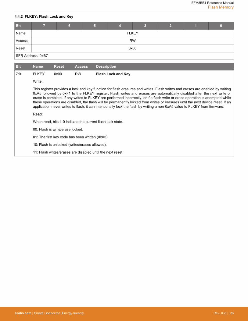
4.4.2 FLKEY: Flash Lock and Key
Bit 7 6 5 4 3 2 1 0
Name FLKEY
Access RW
Reset 0x00
SFR Address: 0xB7
Bit Name Reset Access Description
7:0 FLKEY 0x00 RW Flash Lock and Key.
Write:
This register provides a lock and key function for flash erasures and writes. Flash writes and erases are enabled by writing0xA5 followed by 0xF1 to the FLKEY register. Flash writes and erases are automatically disabled after the next write orerase is complete. If any writes to FLKEY are performed incorrectly, or if a flash write or erase operation is attempted whilethese operations are disabled, the flash will be permanently locked from writes or erasures until the next device reset. If anapplication never writes to flash, it can intentionally lock the flash by writing a non-0xA5 value to FLKEY from firmware.
Read:
When read, bits 1-0 indicate the current flash lock state.
00: Flash is write/erase locked.
01: The first key code has been written (0xA5).
10: Flash is unlocked (writes/erases allowed).
11: Flash writes/erases are disabled until the next reset.
EFM8BB1 Reference ManualFlash Memory
silabs.com | Smart. Connected. Energy-friendly. Rev. 0.2 | 26

5. Device Identification
5.1 Device Identification
The SFR map includes registers that may be used to identify the device family (DEVICEID), derivative (DERIVID), and revision (RE-VID). These SFRs can be read by firmware at runtime to determine the capabilities of the MCU that is executing code. This allows thesame firmware image to run on MCUs with different memory sizes and peripherals, and dynamically change functionality to suit thecapabilities of that MCU.
5.2 Unique Identifier
A 32-bit unique identifier (UID) is pre-loaded upon device reset into the RAM area on all devices. The UID resides in the last four bytesof XRAM on devices which include XRAM, or the last four bytes of the RAM space for devices without XRAM. For devices with the UIDin RAM, the UID can be read by firmware using indirect data accesses. For devices with the UID in XRAM, the UID can be read byfirmware using MOVX instructions. The UID can also be read through the debug port for all devices.
As the UID appears in RAM, firmware can overwrite the UID during normal operation. The bytes in memory will be automatically reini-tialized with the UID value after any device reset. Firmware using this area of memory should always initialize the memory to a knownvalue, as any previous data stored at these locations will be overwritten and not retained through a reset.
Table 5.1. UID Location in Memory
Total Device RAM Memory Segment Addresses
512 Bytes XRAM (MSB) 0x00FF, 0x00FE, 0x00FD, 0x00FC (LSB)
256 Bytes RAM (MSB) 0xFF, 0xFE, 0xFD, 0xFC (LSB)
5.3 Device Identification Registers
5.3.1 DEVICEID: Device Identification
Bit 7 6 5 4 3 2 1 0
Name DEVICEID
Access R
Reset 0x30
SFR Address: 0xB5
Bit Name Reset Access Description
7:0 DEVICEID 0x30 R Device ID.
This read-only register returns the 8-bit device ID.
EFM8BB1 Reference ManualDevice Identification
silabs.com | Smart. Connected. Energy-friendly. Rev. 0.2 | 27

5.3.2 DERIVID: Derivative Identification
Bit 7 6 5 4 3 2 1 0
Name DERIVID
Access R
Reset Varies
SFR Address: 0xAD
Bit Name Reset Access Description
7:0 DERIVID Varies R Derivative ID.
This read-only register returns the 8-bit derivative ID, which can be used by firmware to identify which device in the productfamily the code is executing on. The '{R}' tag in the part numbers indicates the device revision letter in the ordering code.The revision letter may be determined by decoding the REVID register.
Value Name Description
0x01 EFM8BB10F8G_QSOP24
EFM8BB10F8G-{R}-QSOP24
0x02 EFM8BB10F8G_QFN20 EFM8BB10F8G-{R}-QFN20
0x03 EFM8BB10F8G_SO-IC16
EFM8BB10F8G-{R}-SOIC16
0x05 EFM8BB10F4G_QFN20 EFM8BB10F4G-{R}-QFN20
0x08 EFM8BB10F2G_QFN20 EFM8BB10F2G-{R}-QFN20
5.3.3 REVID: Revision Identifcation
Bit 7 6 5 4 3 2 1 0
Name REVID
Access R
Reset Varies
SFR Address: 0xB6
Bit Name Reset Access Description
7:0 REVID Varies R Revision ID.
This read-only register returns the 8-bit revision ID.
Value Name Description
0x02 REV_A Revision A
EFM8BB1 Reference ManualDevice Identification
silabs.com | Smart. Connected. Energy-friendly. Rev. 0.2 | 28

6. Interrupts
6.1 Introduction
The MCU core includes an extended interrupt system supporting multiple interrupt sources and priority levels. The allocation of interruptsources between on-chip peripherals and external input pins varies according to the specific version of the device.
Interrupt sources may have one or more associated interrupt-pending flag(s) located in an SFR local to the associated peripheral.When a peripheral or external source meets a valid interrupt condition, the associated interrupt-pending flag is set to logic 1.
If interrupts are enabled for the source, an interrupt request is generated when the interrupt-pending flag is set. As soon as execution ofthe current instruction is complete, the CPU generates an LCALL to a predetermined address to begin execution of an interrupt serviceroutine (ISR). Each ISR must end with an RETI instruction, which returns program execution to the next instruction that would havebeen executed if the interrupt request had not occurred. If interrupts are not enabled, the interrupt-pending flag is ignored by the hard-ware and program execution continues as normal. The interrupt-pending flag is set to logic 1 regardless of whether the interrupt is ena-bled.
Each interrupt source can be individually enabled or disabled through the use of an associated interrupt enable bit in the IE and EIEnregisters. However, interrupts must first be globally enabled by setting the EA bit to logic 1 before the individual interrupt enables arerecognized. Setting the EA bit to logic 0 disables all interrupt sources regardless of the individual interrupt-enable settings.
Some interrupt-pending flags are automatically cleared by the hardware when the CPU vectors to the ISR or by other hardware condi-tions. However, most are not cleared by the hardware and must be cleared by software before returning from the ISR. If an interrupt-pending flag remains set after the CPU completes the return-from-interrupt (RETI) instruction, a new interrupt request will be generatedimmediately and the CPU will re-enter the ISR after the completion of the next instruction.
6.2 Interrupt Sources and Vectors
The CIP51 core supports interrupt sources for each peripheral on the device. Software can simulate an interrupt for many peripheralsby setting any interrupt-pending flag to logic 1. If interrupts are enabled for the flag, an interrupt request will be generated and the CPUwill vector to the ISR address associated with the interrupt-pending flag. Refer to the data sheet section associated with a particular on-chip peripheral for information regarding valid interrupt conditions for the peripheral and the behavior of its interrupt-pending flag(s).
6.2.1 Interrupt Priorities
Each interrupt source can be individually programmed to one of two priority levels: low or high. A low priority interrupt service routinecan be preempted by a high priority interrupt. A high priority interrupt cannot be preempted. Each interrupt has an associated interruptpriority bit in the IP and EIPn registers, which are used to configure its priority level. Low priority is the default. If two interrupts arerecognized simultaneously, the interrupt with the higher priority is serviced first. If both interrupts have the same priority level, a fixedorder is used to arbitrate, based on the interrupt source's location in the interrupt vector table. Interrupts with a lower number in thevector table have priority.
6.2.2 Interrupt Latency
Interrupt response time depends on the state of the CPU when the interrupt occurs. Pending interrupts are sampled and priority deco-ded on every system clock cycle. Therefore, the fastest possible response time is 5 system clock cycles: 1 clock cycle to detect theinterrupt and 4 clock cycles to complete the LCALL to the ISR. If an interrupt is pending when a RETI is executed, a single instruction isexecuted before an LCALL is made to service the pending interrupt. Therefore, the maximum response time for an interrupt (when noother interrupt is currently being serviced or the new interrupt is of greater priority) occurs when the CPU is performing an RETI instruc-tion followed by a DIV as the next instruction. In this case, the response time is 18 system clock cycles: 1 clock cycle to detect theinterrupt, 5 clock cycles to execute the RETI, 8 clock cycles to complete the DIV instruction and 4 clock cycles to execute the LCALL tothe ISR. If the CPU is executing an ISR for an interrupt with equal or higher priority, the new interrupt will not be serviced until thecurrent ISR completes, including the RETI and following instruction. If more than one interrupt is pending when the CPU exits an ISR,the CPU will service the next highest priority interrupt that is pending.
EFM8BB1 Reference ManualInterrupts
silabs.com | Smart. Connected. Energy-friendly. Rev. 0.2 | 29

6.2.3 Interrupt Summary
Table 6.1. Interrupt Priority Table
Interrupt Source Vector Priority Primary Enable Auxiliary Enable(s) Pending Flag(s)
Reset 0x0000 Top - - -
External Interrupt 0 0x0003 0 IE_EX0 - TCON_IE0
Timer 0 Overflow 0x000B 1 IE_ET0 - TCON_TF0
External Interrupt 1 0x0013 2 IE_EX1 - TCON_IE1
Timer 1 Overflow 0x001B 3 IE_ET1 - TCON_TF1
UART0 0x0023 4 IE_ES0 - SCON0_RI
SCON0_TI
Timer 2 Overflow / Cap-ture
0x002B 5 IE_ET2 TMR2CN0_TF2CEN
TMR2CN0_TF2LEN
TMR2CN0_TF2H
TMR2CN0_TF2L
SPI0 0x0033 6 IE_ESPI0 - SPI0CN0_MODF
SPI0CN0_RXOVRN
SPI0CN0_SPIF
SPI0CN0_WCOL
SMBus 0 0x003B 7 EIE1_ESMB0 - SMB0CN0_SI
Port Match 0x0043 8 EIE1_EMAT - -
ADC0 Window Compare 0x004B 9 EIE1_EWADC0 - ADC0CN0_ADWINT
ADC0 End of Conversion 0x0053 10 EIE1_EADC0 - ADC0CN0_ADINT
PCA0 0x005B 11 EIE1_EPCA0 PCA0CPM0_ECCF
PCA0CPM1_ECCF
PCA0CPM2_ECCF
PCA0PWM_ECOV
PCA0CN0_CCF0
PCA0CN0_CCF1
PCA0CN0_CCF2
PCA0CN0_CF
PCA0PWM_COVF
Comparator 0 0x0063 12 EIE1_ECP0 CMP0MD_CPRIE
CMP0MD_CPFIE
CMP0CN0_CPFIF
CMP0CN0_CPRIF
Comparator 1 0x006B 13 EIE1_ECP1 CMP1MD_CPFIE
CMP1MD_CPRIE
CMP1CN0_CPFIF
CMP1CN0_CPRIF
Timer 3 Overflow / Cap-ture
0x0073 14 EIE1_ET3 TMR3CN0_TF3CEN
TMR3CN0_TF3LEN
TMR3CN0_TF3H
TMR3CN0_TF3L
EFM8BB1 Reference ManualInterrupts
silabs.com | Smart. Connected. Energy-friendly. Rev. 0.2 | 30
6.3 Interrupt Control Registers
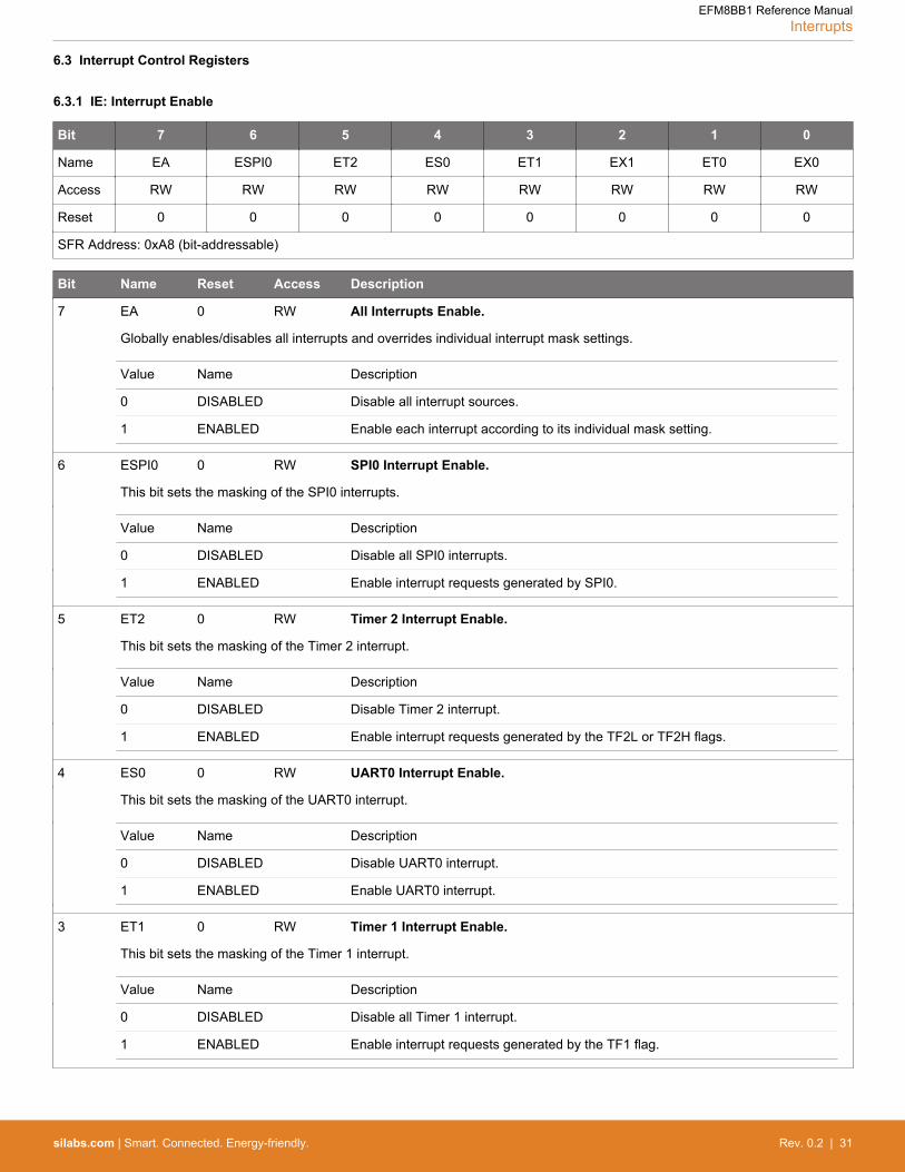
6.3.1 IE: Interrupt Enable
Bit 7 6 5 4 3 2 1 0
Name EA ESPI0 ET2 ES0 ET1 EX1 ET0 EX0
Access RW RW RW RW RW RW RW RW
Reset 0 0 0 0 0 0 0 0
SFR Address: 0xA8 (bit-addressable)
Bit Name Reset Access Description
7 EA 0 RW All Interrupts Enable.
Globally enables/disables all interrupts and overrides individual interrupt mask settings.
Value Name Description
0 DISABLED Disable all interrupt sources.
1 ENABLED Enable each interrupt according to its individual mask setting.
6 ESPI0 0 RW SPI0 Interrupt Enable.
This bit sets the masking of the SPI0 interrupts.
Value Name Description
0 DISABLED Disable all SPI0 interrupts.
1 ENABLED Enable interrupt requests generated by SPI0.
5 ET2 0 RW Timer 2 Interrupt Enable.
This bit sets the masking of the Timer 2 interrupt.
Value Name Description
0 DISABLED Disable Timer 2 interrupt.
1 ENABLED Enable interrupt requests generated by the TF2L or TF2H flags.
4 ES0 0 RW UART0 Interrupt Enable.
This bit sets the masking of the UART0 interrupt.
Value Name Description
0 DISABLED Disable UART0 interrupt.
1 ENABLED Enable UART0 interrupt.
3 ET1 0 RW Timer 1 Interrupt Enable.
This bit sets the masking of the Timer 1 interrupt.
Value Name Description
0 DISABLED Disable all Timer 1 interrupt.
1 ENABLED Enable interrupt requests generated by the TF1 flag.
EFM8BB1 Reference ManualInterrupts
silabs.com | Smart. Connected. Energy-friendly. Rev. 0.2 | 31
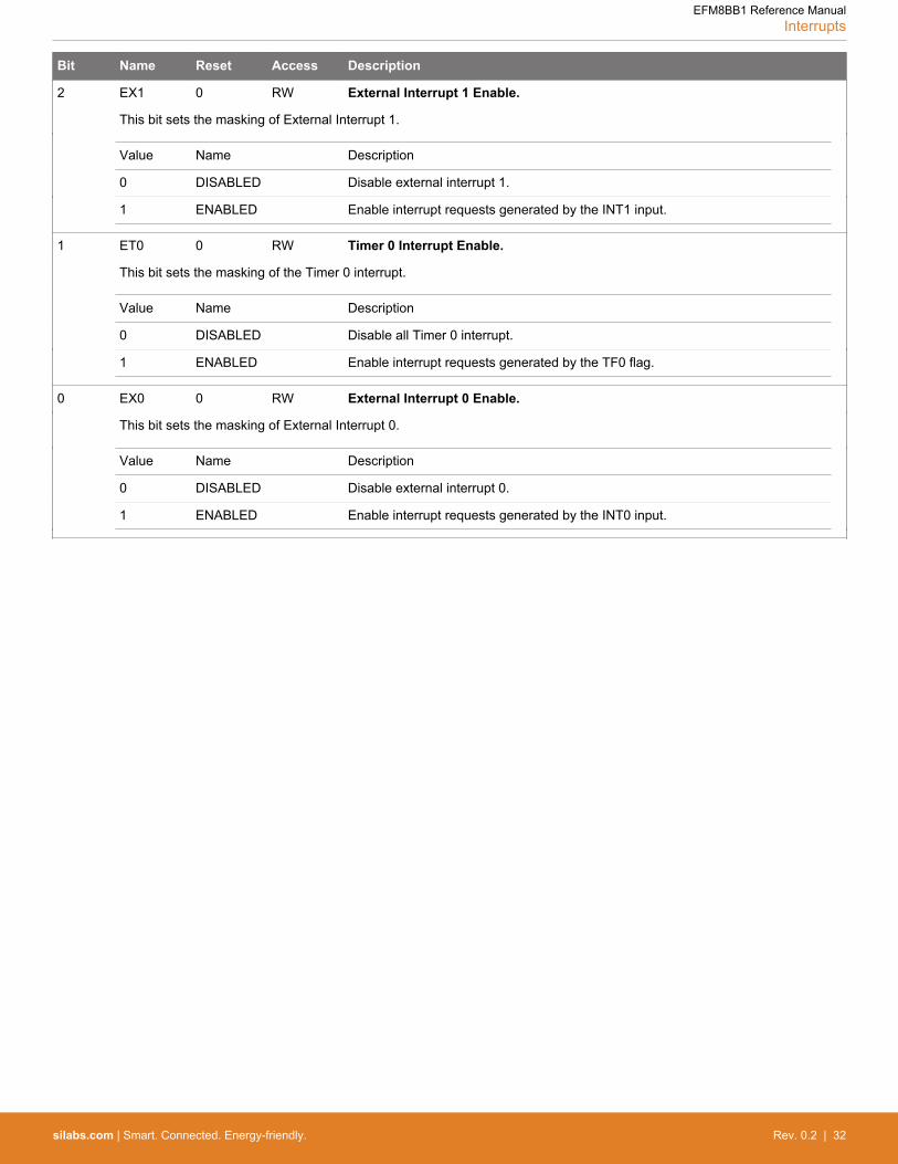
Bit Name Reset Access Description
2 EX1 0 RW External Interrupt 1 Enable.
This bit sets the masking of External Interrupt 1.
Value Name Description
0 DISABLED Disable external interrupt 1.
1 ENABLED Enable interrupt requests generated by the INT1 input.
1 ET0 0 RW Timer 0 Interrupt Enable.
This bit sets the masking of the Timer 0 interrupt.
Value Name Description
0 DISABLED Disable all Timer 0 interrupt.
1 ENABLED Enable interrupt requests generated by the TF0 flag.
0 EX0 0 RW External Interrupt 0 Enable.
This bit sets the masking of External Interrupt 0.
Value Name Description
0 DISABLED Disable external interrupt 0.
1 ENABLED Enable interrupt requests generated by the INT0 input.
EFM8BB1 Reference ManualInterrupts
silabs.com | Smart. Connected. Energy-friendly. Rev. 0.2 | 32

6.3.2 IP: Interrupt Priority
Bit 7 6 5 4 3 2 1 0
Name Reserved PSPI0 PT2 PS0 PT1 PX1 PT0 PX0
Access R RW RW RW RW RW RW RW
Reset 1 0 0 0 0 0 0 0
SFR Address: 0xB8 (bit-addressable)
Bit Name Reset Access Description
7 Reserved Must write reset value.
6 PSPI0 0 RW Serial Peripheral Interface (SPI0) Interrupt Priority Control.
This bit sets the priority of the SPI0 interrupt.
Value Name Description
0 LOW SPI0 interrupt set to low priority level.
1 HIGH SPI0 interrupt set to high priority level.
5 PT2 0 RW Timer 2 Interrupt Priority Control.
This bit sets the priority of the Timer 2 interrupt.
Value Name Description
0 LOW Timer 2 interrupt set to low priority level.
1 HIGH Timer 2 interrupt set to high priority level.
4 PS0 0 RW UART0 Interrupt Priority Control.
This bit sets the priority of the UART0 interrupt.
Value Name Description
0 LOW UART0 interrupt set to low priority level.
1 HIGH UART0 interrupt set to high priority level.
3 PT1 0 RW Timer 1 Interrupt Priority Control.
This bit sets the priority of the Timer 1 interrupt.
Value Name Description
0 LOW Timer 1 interrupt set to low priority level.
1 HIGH Timer 1 interrupt set to high priority level.
2 PX1 0 RW External Interrupt 1 Priority Control.
This bit sets the priority of the External Interrupt 1 interrupt.
Value Name Description
0 LOW External Interrupt 1 set to low priority level.
1 HIGH External Interrupt 1 set to high priority level.
1 PT0 0 RW Timer 0 Interrupt Priority Control.
This bit sets the priority of the Timer 0 interrupt.
EFM8BB1 Reference ManualInterrupts
silabs.com | Smart. Connected. Energy-friendly. Rev. 0.2 | 33

Bit Name Reset Access Description
Value Name Description
0 LOW Timer 0 interrupt set to low priority level.
1 HIGH Timer 0 interrupt set to high priority level.
0 PX0 0 RW External Interrupt 0 Priority Control.
This bit sets the priority of the External Interrupt 0 interrupt.
Value Name Description
0 LOW External Interrupt 0 set to low priority level.
1 HIGH External Interrupt 0 set to high priority level.
EFM8BB1 Reference ManualInterrupts
silabs.com | Smart. Connected. Energy-friendly. Rev. 0.2 | 34

6.3.3 EIE1: Extended Interrupt Enable 1
Bit 7 6 5 4 3 2 1 0
Name ET3 ECP1 ECP0 EPCA0 EADC0 EWADC0 EMAT ESMB0
Access RW RW RW RW RW RW RW RW
Reset 0 0 0 0 0 0 0 0
SFR Address: 0xE6
Bit Name Reset Access Description
7 ET3 0 RW Timer 3 Interrupt Enable.
This bit sets the masking of the Timer 3 interrupt.
Value Name Description
0 DISABLED Disable Timer 3 interrupts.
1 ENABLED Enable interrupt requests generated by the TF3L or TF3H flags.
6 ECP1 0 RW Comparator1 (CP1) Interrupt Enable.
This bit sets the masking of the CP1 interrupt.
Value Name Description
0 DISABLED Disable CP1 interrupts.
1 ENABLED Enable interrupt requests generated by the comparator 1 CPRIF or CPFIF flags.
5 ECP0 0 RW Comparator0 (CP0) Interrupt Enable.
This bit sets the masking of the CP0 interrupt.
Value Name Description
0 DISABLED Disable CP0 interrupts.
1 ENABLED Enable interrupt requests generated by the comparator 0 CPRIF or CPFIF flags.
4 EPCA0 0 RW Programmable Counter Array (PCA0) Interrupt Enable.
This bit sets the masking of the PCA0 interrupts.
Value Name Description
0 DISABLED Disable all PCA0 interrupts.
1 ENABLED Enable interrupt requests generated by PCA0.
3 EADC0 0 RW ADC0 Conversion Complete Interrupt Enable.
This bit sets the masking of the ADC0 Conversion Complete interrupt.
Value Name Description
0 DISABLED Disable ADC0 Conversion Complete interrupt.
1 ENABLED Enable interrupt requests generated by the ADINT flag.
2 EWADC0 0 RW ADC0 Window Comparison Interrupt Enable.
This bit sets the masking of ADC0 Window Comparison interrupt.
EFM8BB1 Reference ManualInterrupts
silabs.com | Smart. Connected. Energy-friendly. Rev. 0.2 | 35

Bit Name Reset Access Description
Value Name Description
0 DISABLED Disable ADC0 Window Comparison interrupt.
1 ENABLED Enable interrupt requests generated by ADC0 Window Compare flag (ADWINT).
1 EMAT 0 RW Port Match Interrupts Enable.
This bit sets the masking of the Port Match Event interrupt.
Value Name Description
0 DISABLED Disable all Port Match interrupts.
1 ENABLED Enable interrupt requests generated by a Port Match.
0 ESMB0 0 RW SMBus (SMB0) Interrupt Enable.
This bit sets the masking of the SMB0 interrupt.
Value Name Description
0 DISABLED Disable all SMB0 interrupts.
1 ENABLED Enable interrupt requests generated by SMB0.
EFM8BB1 Reference ManualInterrupts
silabs.com | Smart. Connected. Energy-friendly. Rev. 0.2 | 36

6.3.4 EIP1: Extended Interrupt Priority 1
Bit 7 6 5 4 3 2 1 0
Name PT3 PCP1 PCP0 PPCA0 PADC0 PWADC0 PMAT PSMB0
Access RW RW RW RW RW RW RW RW
Reset 0 0 0 0 0 0 0 0
SFR Address: 0xF3
Bit Name Reset Access Description
7 PT3 0 RW Timer 3 Interrupt Priority Control.
This bit sets the priority of the Timer 3 interrupt.
Value Name Description
0 LOW Timer 3 interrupts set to low priority level.
1 HIGH Timer 3 interrupts set to high priority level.
6 PCP1 0 RW Comparator1 (CP1) Interrupt Priority Control.
This bit sets the priority of the CP1 interrupt.
Value Name Description
0 LOW CP1 interrupt set to low priority level.
1 HIGH CP1 interrupt set to high priority level.
5 PCP0 0 RW Comparator0 (CP0) Interrupt Priority Control.
This bit sets the priority of the CP0 interrupt.
Value Name Description
0 LOW CP0 interrupt set to low priority level.
1 HIGH CP0 interrupt set to high priority level.
4 PPCA0 0 RW Programmable Counter Array (PCA0) Interrupt Priority Control.
This bit sets the priority of the PCA0 interrupt.
Value Name Description
0 LOW PCA0 interrupt set to low priority level.
1 HIGH PCA0 interrupt set to high priority level.
3 PADC0 0 RW ADC0 Conversion Complete Interrupt Priority Control.
This bit sets the priority of the ADC0 Conversion Complete interrupt.
Value Name Description
0 LOW ADC0 Conversion Complete interrupt set to low priority level.
1 HIGH ADC0 Conversion Complete interrupt set to high priority level.
2 PWADC0 0 RW ADC0 Window Comparator Interrupt Priority Control.
This bit sets the priority of the ADC0 Window interrupt.
EFM8BB1 Reference ManualInterrupts
silabs.com | Smart. Connected. Energy-friendly. Rev. 0.2 | 37

Bit Name Reset Access Description
Value Name Description
0 LOW ADC0 Window interrupt set to low priority level.
1 HIGH ADC0 Window interrupt set to high priority level.
1 PMAT 0 RW Port Match Interrupt Priority Control.
This bit sets the priority of the Port Match Event interrupt.
Value Name Description
0 LOW Port Match interrupt set to low priority level.
1 HIGH Port Match interrupt set to high priority level.
0 PSMB0 0 RW SMBus (SMB0) Interrupt Priority Control.
This bit sets the priority of the SMB0 interrupt.
Value Name Description
0 LOW SMB0 interrupt set to low priority level.
1 HIGH SMB0 interrupt set to high priority level.
EFM8BB1 Reference ManualInterrupts
silabs.com | Smart. Connected. Energy-friendly. Rev. 0.2 | 38

7. Power Management and Internal Regulators
7.1 Introduction
All internal circuitry draws power from the VDD supply pin. External I/O pins are powered from the VIO supply voltage (or VDD on devi-ces without a separate VIO connection), while most of the internal circuitry is supplied by an on-chip LDO regulator. Control over thedevice power can be achieved by enabling/disabling individual peripherals as needed. Each analog peripheral can be disabled whennot in use and placed in low power mode. Digital peripherals, such as timers and serial buses, have their clocks gated off and draw littlepower when they are not in use.
Power Distribution
Core LDO
Analog Muxes
VDD
GND
Digital I/O Interface
Port I/O PinsCPU Core
RAM
Flash
Oscillators
1.8V
Peripheral Logic
Figure 7.1. Power System Block Diagram
Table 7.1. Power Modes
Power Mode Details Mode Entry Wake-Up Sources
Normal Core and all peripherals clocked and fully operational — —
Idle • Core halted• All peripherals clocked and fully operational• Code resumes execution on wake event
Set IDLE bit in PCON0 Any interrupt
Shutdown • All internal power nets shut down• Pins retain state• Exit on pin or power-on reset
1. Set STOPCF bit inREG0CN
2. Set STOP bit inPCON0
• RSTb pin reset• Power-on reset
EFM8BB1 Reference ManualPower Management and Internal Regulators
silabs.com | Smart. Connected. Energy-friendly. Rev. 0.2 | 39

7.2 Features
• Supports four power modes:1. Normal mode: Core and all peripherals fully operational.2. Idle mode: Core halted, peripherals fully operational, core waiting for interrupt to continue.3. Shutdown mode: All clocks stopped and internal LDO shut off, device waiting for POR or pin reset.
Note: Legacy 8051 Stop mode is also supported, where internal LDO remains active, but a device reset is required to wake.• Fully internal core LDO supplies power to majority of blocks.
7.3 Idle Mode
In idle mode, CPU core execution is halted while any enabled peripherals and clocks remain active. Power consumption in idle mode isdependent upon the system clock frequency and any active peripherals.
Setting the IDLE bit in the PCON0 register causes the hardware to halt the CPU and enter idle mode as soon as the instruction thatsets the bit completes execution. All internal registers and memory maintain their original data. All analog and digital peripherals canremain active during idle mode.
Idle mode is terminated when an enabled interrupt is asserted or a reset occurs. The assertion of an enabled interrupt will cause theIDLE bit to be cleared and the CPU to resume operation. The pending interrupt will be serviced and the next instruction to be executedafter the return from interrupt (RETI) will be the instruction immediately following the one that set the IDLE bit. If idle mode is terminatedby an internal or external reset, the CIP-51 performs a normal reset sequence and begins program execution at address 0x0000.Note: If the instruction following the write of the IDLE bit is a single-byte instruction and an interrupt occurs during the execution phaseof the instruction that sets the IDLE bit, the CPU may not wake from idle mode when a future interrupt occurs. Therefore, instructionsthat set the IDLE bit should be followed by an instruction that has two or more opcode bytes. For example:
// in ‘C’: PCON0 |= 0x01; // set IDLE bit PCON0 = PCON0; // ... followed by a 3-cycle dummy instruction
; in assembly: ORL PCON0, #01h ; set IDLE bit MOV PCON0, PCON0 ; ... followed by a 3-cycle dummy instruction
If enabled, the Watchdog Timer (WDT) will eventually cause an internal watchdog reset and thereby terminate the Idle mode. This fea-ture protects the system from an unintended permanent shutdown in the event of an inadvertent write to the PCON0 register. If thisbehavior is not desired, the WDT may be disabled by software prior to entering the idle mode if the WDT was initially configured toallow this operation. This provides the opportunity for additional power savings, allowing the system to remain in the idle mode indefi-nitely, waiting for an external stimulus to wake up the system.
7.4 Stop Mode
In stop mode, the CPU is halted and peripheral clocks are stopped. Analog peripherals remain in their selected states.
Setting the STOP bit in the PCON0 register causes the controller core to enter stop mode as soon as the instruction that sets the bitcompletes execution. Before entering stop mode, the system clock must be sourced by HFOSC0. In stop mode, the CPU and internalclocks are stopped. Analog peripherals may remain enabled, but will not be provided a clock. Each analog peripheral may be shut downindividually by firmware prior to entering stop mode. Stop mode can only be terminated by an internal or external reset. On reset, thedevice performs the normal reset sequence and begins program execution at address 0x0000.
If enabled as a reset source, the missing clock detector will cause an internal reset and thereby terminate the stop mode. If this reset isundesirable in the system, and the CPU is to be placed in stop mode for longer than the missing clock detector timeout, the missingclock detector should be disabled in firmware prior to setting the STOP bit.
EFM8BB1 Reference ManualPower Management and Internal Regulators
silabs.com | Smart. Connected. Energy-friendly. Rev. 0.2 | 40

7.5 Shutdown Mode
In shutdown mode, the CPU is halted and the internal LDO is powered down. External I/O will retain their configured states.
To enter Shutdown mode, firmware should set the STOPCF bit in the regulator control register to 1, and then set the STOP bit inPCON0. In Shutdown, the RSTb pin and a full power cycle of the device are the only methods of generating a reset and waking thedevice.Note: In Shutdown mode, all internal device circuitry is powered down, and no RAM nor registers are retained. The debug circuitry willnot be able to connect to a device while it is in Shutdown. Coming out of Shutdown mode, whether by POR or pin reset, will appear asa power-on reset of the device.
7.6 Power Management Control Registers
7.6.1 PCON0: Power Control
Bit 7 6 5 4 3 2 1 0
Name GF5 GF4 GF3 GF2 GF1 GF0 STOP IDLE
Access RW RW RW RW RW RW RW RW
Reset 0 0 0 0 0 0 0 0
SFR Address: 0x87
Bit Name Reset Access Description
7 GF5 0 RW General Purpose Flag 5.
This flag is a general purpose flag for use under firmware control.
6 GF4 0 RW General Purpose Flag 4.
This flag is a general purpose flag for use under firmware control.
5 GF3 0 RW General Purpose Flag 3.
This flag is a general purpose flag for use under firmware control.
4 GF2 0 RW General Purpose Flag 2.
This flag is a general purpose flag for use under firmware control.
3 GF1 0 RW General Purpose Flag 1.
This flag is a general purpose flag for use under firmware control.
2 GF0 0 RW General Purpose Flag 0.
This flag is a general purpose flag for use under firmware control.
1 STOP 0 RW Stop Mode Select.
Setting this bit will place the CIP-51 in Stop mode. This bit will always be read as 0.
0 IDLE 0 RW Idle Mode Select.
Setting this bit will place the CIP-51 in Idle mode. This bit will always be read as 0.
EFM8BB1 Reference ManualPower Management and Internal Regulators
silabs.com | Smart. Connected. Energy-friendly. Rev. 0.2 | 41

7.6.2 REG0CN: Voltage Regulator 0 Control
Bit 7 6 5 4 3 2 1 0
Name Reserved STOPCF Reserved
Access R RW R
Reset 0x0 0 0x0
SFR Address: 0xC9
Bit Name Reset Access Description
7:4 Reserved Must write reset value.
3 STOPCF 0 RW Stop Mode Configuration.
This bit configures the regulator's behavior when the device enters stop mode.
Value Name Description
0 ACTIVE Regulator is still active in stop mode. Any enabled reset source will reset the de-vice.
1 SHUTDOWN Regulator is shut down in stop mode. Only the RSTb pin or power cycle can resetthe device.
2:0 Reserved Must write reset value.
EFM8BB1 Reference ManualPower Management and Internal Regulators
silabs.com | Smart. Connected. Energy-friendly. Rev. 0.2 | 42
8. Clocking and Oscillators
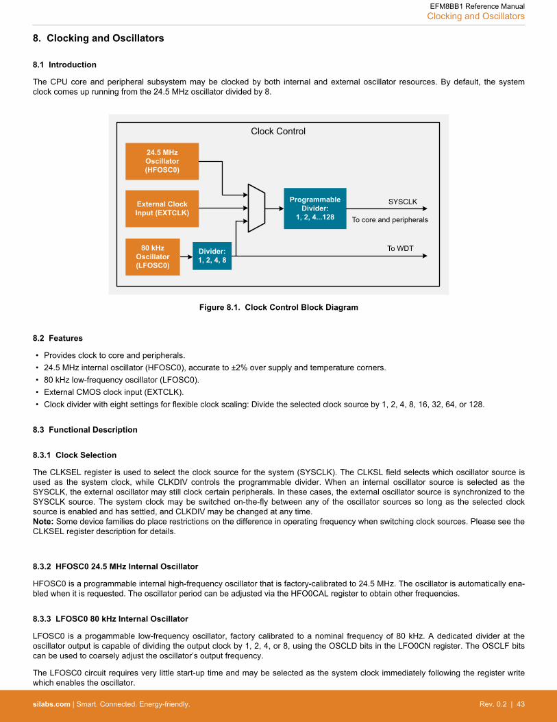
8.1 Introduction
The CPU core and peripheral subsystem may be clocked by both internal and external oscillator resources. By default, the systemclock comes up running from the 24.5 MHz oscillator divided by 8.
Clock Control
Programmable Divider:
1, 2, 4...128
SYSCLK
80 kHz Oscillator(LFOSC0)
24.5 MHz Oscillator(HFOSC0)
External Clock Input (EXTCLK)
Divider:1, 2, 4, 8
To WDT
To core and peripherals
Figure 8.1. Clock Control Block Diagram
8.2 Features
• Provides clock to core and peripherals.• 24.5 MHz internal oscillator (HFOSC0), accurate to ±2% over supply and temperature corners.• 80 kHz low-frequency oscillator (LFOSC0).• External CMOS clock input (EXTCLK).• Clock divider with eight settings for flexible clock scaling: Divide the selected clock source by 1, 2, 4, 8, 16, 32, 64, or 128.
8.3 Functional Description
8.3.1 Clock Selection
The CLKSEL register is used to select the clock source for the system (SYSCLK). The CLKSL field selects which oscillator source isused as the system clock, while CLKDIV controls the programmable divider. When an internal oscillator source is selected as theSYSCLK, the external oscillator may still clock certain peripherals. In these cases, the external oscillator source is synchronized to theSYSCLK source. The system clock may be switched on-the-fly between any of the oscillator sources so long as the selected clocksource is enabled and has settled, and CLKDIV may be changed at any time.Note: Some device families do place restrictions on the difference in operating frequency when switching clock sources. Please see theCLKSEL register description for details.
8.3.2 HFOSC0 24.5 MHz Internal Oscillator
HFOSC0 is a programmable internal high-frequency oscillator that is factory-calibrated to 24.5 MHz. The oscillator is automatically ena-bled when it is requested. The oscillator period can be adjusted via the HFO0CAL register to obtain other frequencies.
8.3.3 LFOSC0 80 kHz Internal Oscillator
LFOSC0 is a progammable low-frequency oscillator, factory calibrated to a nominal frequency of 80 kHz. A dedicated divider at theoscillator output is capable of dividing the output clock by 1, 2, 4, or 8, using the OSCLD bits in the LFO0CN register. The OSCLF bitscan be used to coarsely adjust the oscillator’s output frequency.
The LFOSC0 circuit requires very little start-up time and may be selected as the system clock immediately following the register writewhich enables the oscillator.
EFM8BB1 Reference ManualClocking and Oscillators
silabs.com | Smart. Connected. Energy-friendly. Rev. 0.2 | 43

Calibrating LFOSC0
On-chip calibration of the LFOSC0 can be performed using a timer to capture the oscillator period, when running from a known timebase. When a timer is configured for L-F Oscillator capture mode, a rising edge of the low-frequency oscillator’s output will cause acapture event on the corresponding timer. As a capture event occurs, the current timer value is copied into the timer reload registers.By recording the difference between two successive timer capture values, the low-frequency oscillator’s period can be calculated. TheOSCLF bits can then be adjusted to produce the desired oscillator frequency.
8.3.4 External Clock
An external CMOS clock source is also supported as a core clock source. The EXTCLK pin on the device serves as the external clockinput when running in this mode. The EXTCLK input may also be used to clock certain digital peripherals (e.g., Timers, PCA, etc.) whileSYSCLK runs from one of the internal oscillator sources. When not selected as the SYSCLK source, the EXTCLK input is always re-synchronized to SYSCLK.Note: When selecting the EXTCLK pin as a clock input source, the pin should be skipped in the crossbar and configured as a digitalinput. Firmware should ensure that the external clock source is present or enable the missing clock detector before switching theCLKSL field.
EFM8BB1 Reference ManualClocking and Oscillators
silabs.com | Smart. Connected. Energy-friendly. Rev. 0.2 | 44

8.4 Clocking and Oscillator Control Registers
8.4.1 CLKSEL: Clock Select
Bit 7 6 5 4 3 2 1 0
Name Reserved CLKDIV Reserved CLKSL
Access R RW R RW
Reset 0 0x3 0x0 0x0
SFR Address: 0xA9
Bit Name Reset Access Description
7 Reserved Must write reset value.
6:4 CLKDIV 0x3 RW Clock Source Divider.
This field controls the divider applied to the clock source selected by CLKSL. The output of this divider is the system clock(SYSCLK).
Value Name Description
0x0 SYSCLK_DIV_1 SYSCLK is equal to selected clock source divided by 1.
0x1 SYSCLK_DIV_2 SYSCLK is equal to selected clock source divided by 2.
0x2 SYSCLK_DIV_4 SYSCLK is equal to selected clock source divided by 4.
0x3 SYSCLK_DIV_8 SYSCLK is equal to selected clock source divided by 8.
0x4 SYSCLK_DIV_16 SYSCLK is equal to selected clock source divided by 16.
0x5 SYSCLK_DIV_32 SYSCLK is equal to selected clock source divided by 32.
0x6 SYSCLK_DIV_64 SYSCLK is equal to selected clock source divided by 64.
0x7 SYSCLK_DIV_128 SYSCLK is equal to selected clock source divided by 128.
3:2 Reserved Must write reset value.
1:0 CLKSL 0x0 RW Clock Source Select.
Selects the system clock source.
Value Name Description
0x0 HFOSC Clock derived from the Internal High-Frequency Oscillator.
0x1 EXTOSC Clock derived from the External CMOS clock circuit.
0x2 LFOSC Clock derived from the Internal Low-Frequency Oscillator.
There are no restrictions when switching between clock sources or divider values for this family.
EFM8BB1 Reference ManualClocking and Oscillators
silabs.com | Smart. Connected. Energy-friendly. Rev. 0.2 | 45

8.4.2 HFO0CAL: High Frequency Oscillator 0 Calibration
Bit 7 6 5 4 3 2 1 0
Name HFO0CAL
Access RW
Reset Varies
SFR Address: 0xC7
Bit Name Reset Access Description
7:0 HFO0CAL Varies RW Oscillator Calibration.
These bits determine the period for high frequency oscillator 0. When set to 0x00, the oscillator operates at its fastest set-ting. When set to 0xFF, the oscillator operates at its slowest setting. The reset value is factory calibrated, and the oscillatorwill revert to the calibrated frequency upon reset.
EFM8BB1 Reference ManualClocking and Oscillators
silabs.com | Smart. Connected. Energy-friendly. Rev. 0.2 | 46
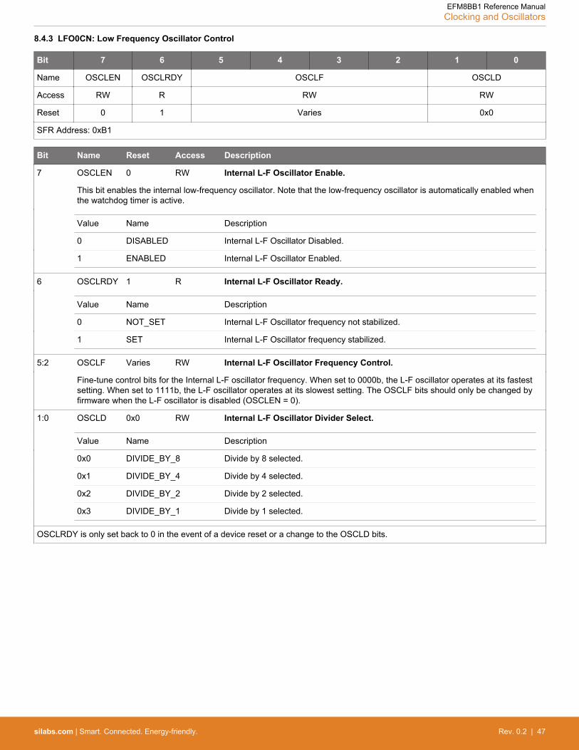
8.4.3 LFO0CN: Low Frequency Oscillator Control
Bit 7 6 5 4 3 2 1 0
Name OSCLEN OSCLRDY OSCLF OSCLD
Access RW R RW RW
Reset 0 1 Varies 0x0
SFR Address: 0xB1
Bit Name Reset Access Description
7 OSCLEN 0 RW Internal L-F Oscillator Enable.
This bit enables the internal low-frequency oscillator. Note that the low-frequency oscillator is automatically enabled whenthe watchdog timer is active.
Value Name Description
0 DISABLED Internal L-F Oscillator Disabled.
1 ENABLED Internal L-F Oscillator Enabled.
6 OSCLRDY 1 R Internal L-F Oscillator Ready.
Value Name Description
0 NOT_SET Internal L-F Oscillator frequency not stabilized.
1 SET Internal L-F Oscillator frequency stabilized.
5:2 OSCLF Varies RW Internal L-F Oscillator Frequency Control.
Fine-tune control bits for the Internal L-F oscillator frequency. When set to 0000b, the L-F oscillator operates at its fastestsetting. When set to 1111b, the L-F oscillator operates at its slowest setting. The OSCLF bits should only be changed byfirmware when the L-F oscillator is disabled (OSCLEN = 0).
1:0 OSCLD 0x0 RW Internal L-F Oscillator Divider Select.
Value Name Description
0x0 DIVIDE_BY_8 Divide by 8 selected.
0x1 DIVIDE_BY_4 Divide by 4 selected.
0x2 DIVIDE_BY_2 Divide by 2 selected.
0x3 DIVIDE_BY_1 Divide by 1 selected.
OSCLRDY is only set back to 0 in the event of a device reset or a change to the OSCLD bits.
EFM8BB1 Reference ManualClocking and Oscillators
silabs.com | Smart. Connected. Energy-friendly. Rev. 0.2 | 47
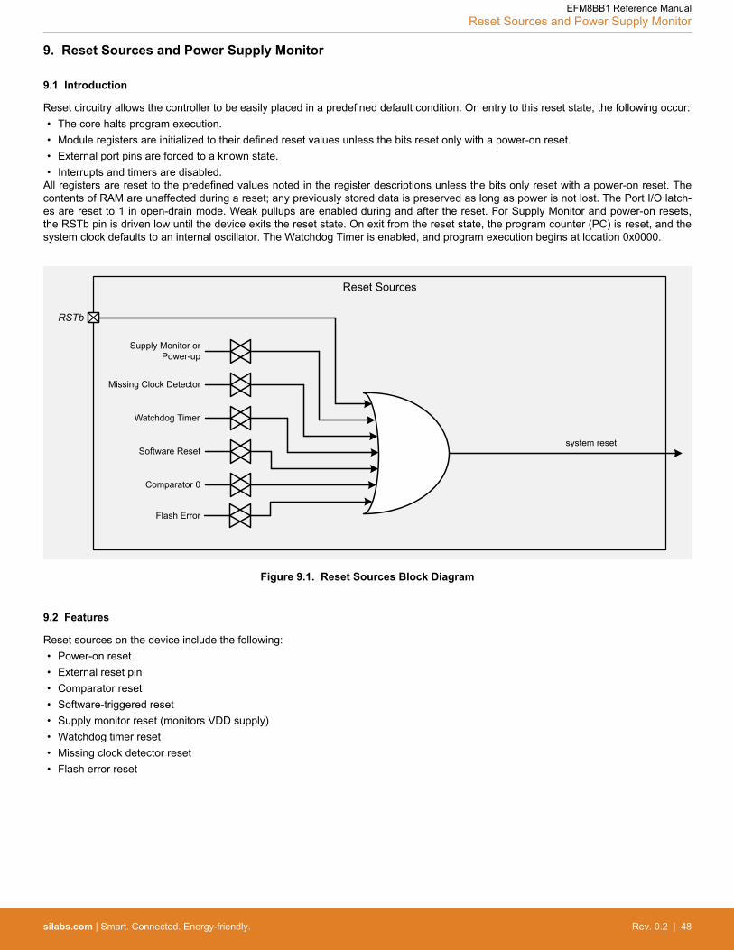
9. Reset Sources and Power Supply Monitor
9.1 Introduction
Reset circuitry allows the controller to be easily placed in a predefined default condition. On entry to this reset state, the following occur:• The core halts program execution.• Module registers are initialized to their defined reset values unless the bits reset only with a power-on reset.• External port pins are forced to a known state.• Interrupts and timers are disabled.
All registers are reset to the predefined values noted in the register descriptions unless the bits only reset with a power-on reset. Thecontents of RAM are unaffected during a reset; any previously stored data is preserved as long as power is not lost. The Port I/O latch-es are reset to 1 in open-drain mode. Weak pullups are enabled during and after the reset. For Supply Monitor and power-on resets,the RSTb pin is driven low until the device exits the reset state. On exit from the reset state, the program counter (PC) is reset, and thesystem clock defaults to an internal oscillator. The Watchdog Timer is enabled, and program execution begins at location 0x0000.
Reset Sources
RSTb
Supply Monitor or Power-up
Missing Clock Detector
Watchdog Timer
Software Reset
Comparator 0
system reset
Flash Error
Figure 9.1. Reset Sources Block Diagram
9.2 Features
Reset sources on the device include the following:• Power-on reset• External reset pin• Comparator reset• Software-triggered reset• Supply monitor reset (monitors VDD supply)• Watchdog timer reset• Missing clock detector reset• Flash error reset
EFM8BB1 Reference ManualReset Sources and Power Supply Monitor
silabs.com | Smart. Connected. Energy-friendly. Rev. 0.2 | 48

9.3 Functional Description
9.3.1 Device Reset
Upon entering a reset state from any source, the following events occur:• The processor core halts program execution.• Special Function Registers (SFRs) are initialized to their defined reset values.• External port pins are placed in a known state.• Interrupts and timers are disabled.
SFRs are reset to the predefined reset values noted in the detailed register descriptions. The contents of internal data memory areunaffected during a reset; any previously stored data is preserved. However, since the stack pointer SFR is reset, the stack is effective-ly lost, even though the data on the stack is not altered.
The port I/O latches are reset to 0xFF (all logic ones) in open-drain mode. Weak pullups are enabled during and after the reset. ForSupply Monitor and power-on resets, the RSTb pin is driven low until the device exits the reset state.Note: During a power-on event, there may be a short delay before the POR circuitry fires and the RSTb pin is driven low. During thattime, the RSTb pin will be weakly pulled to the supply pin.
On exit from the reset state, the program counter (PC) is reset, the watchdog timer is enabled, and the system clock defaults to aninternal oscillator. Program execution begins at location 0x0000.
EFM8BB1 Reference ManualReset Sources and Power Supply Monitor
silabs.com | Smart. Connected. Energy-friendly. Rev. 0.2 | 49

9.3.2 Power-On Reset
During power-up, the POR circuit fires. When POR fires, the device is held in a reset state and the RSTb pin is driven low until thesupply voltage settles above VRST. Two delays are present during the supply ramp time. First, a delay occurs before the POR circuitryfires and pulls the RSTb pin low. A second delay occurs before the device is released from reset; the delay decreases as the supplyramp time increases (supply ramp time is defined as how fast the supply pin ramps from 0 V to VRST). For ramp times less than 1 ms,the power-on reset time (TPOR) is typically less than 0.3 ms. Additionally, the power supply must reach VRST before the POR circuitreleases the device from reset.
On exit from a power-on reset, the PORSF flag is set by hardware to logic 1. When PORSF is set, all of the other reset flags in theRSTSRC register are indeterminate. (PORSF is cleared by all other resets.) Since all resets cause program execution to begin at thesame location (0x0000), software can read the PORSF flag to determine if a power-up was the cause of reset. The content of internaldata memory should be assumed to be undefined after a power-on reset. The supply monitor is enabled following a power-on reset.
Power-On Reset
RSTb
t
volts
Logic HIGH
Logic LOW
TPOR
Supp
ly Vo
ltage
Figure 9.2. Power-On Reset Timing
EFM8BB1 Reference ManualReset Sources and Power Supply Monitor
silabs.com | Smart. Connected. Energy-friendly. Rev. 0.2 | 50

9.3.3 Supply Monitor Reset
The supply monitor senses the voltage on the device's supply pin and can generate a reset if the supply drops below the correspondingthreshold. This monitor is enabled and enabled as a reset source after initial power-on to protect the device until the supply is an ade-quate and stable voltage. When enabled and selected as a reset source, any power down transition or power irregularity that causesthe supply to drop below the reset threshold will drive the RSTb pin low and hold the core in a reset state. When the supply returns to alevel above the reset threshold, the monitor will release the core from the reset state. The reset status can then be read using thedevice reset sources module. After a power-fail reset, the PORF flag reads 1 and all of the other reset flags in the RSTSRC register areindeterminate. The power-on reset delay (tPOR) is not incurred after a supply monitor reset. The contents of RAM should be presumedinvalid after a supply monitor reset. The enable state of the supply monitor and its selection as a reset source is not altered by deviceresets. For example, if the supply monitor is de-selected as a reset source and disabled by software using the VDMEN bit in theVDM0CN register, and then firmware performs a software reset, the supply monitor will remain disabled and de-selected after the reset.To protect the integrity of flash contents, the supply monitor must be enabled and selected as a reset source if software contains rou-tines that erase or write flash memory. If the supply monitor is not enabled, any erase or write performed on flash memory will be ignor-ed.
t
volts
Supply Voltage
Reset Threshold (VRST)
Supply Monitor Reset
RSTb
Figure 9.3. Reset Sources
9.3.4 External Reset
The external RSTb pin provides a means for external circuitry to force the device into a reset state. Asserting an active-low signal onthe RSTb pin generates a reset; an external pullup and/or decoupling of the RSTb pin may be necessary to avoid erroneous noise-induced resets. The PINRSF flag is set on exit from an external reset.
9.3.5 Missing Clock Detector Reset
The Missing Clock Detector (MCD) is a one-shot circuit that is triggered by the system clock. If the system clock remains high or low formore than the MCD time window, the one-shot will time out and generate a reset. After a MCD reset, the MCDRSF flag will read 1,signifying the MCD as the reset source; otherwise, this bit reads 0. Writing a 1 to the MCDRSF bit enables the Missing Clock Detector;writing a 0 disables it. The state of the RSTb pin is unaffected by this reset.
9.3.6 Comparator (CMP0) Reset
Comparator0 can be configured as a reset source by writing a 1 to the C0RSEF flag. Comparator0 should be enabled and allowed tosettle prior to writing to C0RSEF to prevent any turn-on chatter on the output from generating an unwanted reset. The Comparator0reset is active-low: if the non-inverting input voltage (on CP0+) is less than the inverting input voltage (on CP0–), the device is put intothe reset state. After a Comparator0 reset, the C0RSEF flag will read 1 signifying Comparator0 as the reset source; otherwise, this bitreads 0. The state of the RSTb pin is unaffected by this reset.
EFM8BB1 Reference ManualReset Sources and Power Supply Monitor
silabs.com | Smart. Connected. Energy-friendly. Rev. 0.2 | 51

9.3.7 Watchdog Timer Reset
The programmable Watchdog Timer (WDT) can be used to prevent software from running out of control during a system malfunction.The WDT function can be enabled or disabled by software as described in the watchdog timer section. If a system malfunction preventsuser software from updating the WDT, a reset is generated and the WDTRSF bit is set to 1. The state of the RSTb pin is unaffected bythis reset.
9.3.8 Flash Error Reset
If a flash read/write/erase or program read targets an illegal address, a system reset is generated. This may occur due to any of thefollowing:• A flash write or erase is attempted above user code space.• A flash read is attempted above user code space.• A program read is attempted above user code space (i.e., a branch instruction to the reserved area).• A flash read, write or erase attempt is restricted due to a flash security setting.
The FERROR bit is set following a flash error reset. The state of the RSTb pin is unaffected by this reset.
9.3.9 Software Reset
Software may force a reset by writing a 1 to the SWRSF bit. The SWRSF bit will read 1 following a software forced reset. The state ofthe RSTb pin is unaffected by this reset.
EFM8BB1 Reference ManualReset Sources and Power Supply Monitor
silabs.com | Smart. Connected. Energy-friendly. Rev. 0.2 | 52

9.4 Reset Sources and Supply Monitor Control Registers
9.4.1 RSTSRC: Reset Source
Bit 7 6 5 4 3 2 1 0
Name Reserved FERROR C0RSEF SWRSF WDTRSF MCDRSF PORSF PINRSF
Access RW R RW RW R RW RW R
Reset Varies Varies Varies Varies Varies Varies Varies Varies
SFR Address: 0xEF
Bit Name Reset Access Description
7 Reserved Must write reset value.
6 FERROR Varies R Flash Error Reset Flag.
This read-only bit is set to '1' if a flash read/write/erase error caused the last reset.
5 C0RSEF Varies RW Comparator0 Reset Enable and Flag.
Read: This bit reads 1 if Comparator 0 caused the last reset.
Write: Writing a 1 to this bit enables Comparator 0 (active-low) as a reset source.
4 SWRSF Varies RW Software Reset Force and Flag.
Read: This bit reads 1 if last reset was caused by a write to SWRSF.
Write: Writing a 1 to this bit forces a system reset.
3 WDTRSF Varies R Watchdog Timer Reset Flag.
This read-only bit is set to '1' if a watchdog timer overflow caused the last reset.
2 MCDRSF Varies RW Missing Clock Detector Enable and Flag.
Read: This bit reads 1 if a missing clock detector timeout caused the last reset.
Write: Writing a 1 to this bit enables the missing clock detector. The MCD triggers a reset if a missing clock condition isdetected.
1 PORSF Varies RW Power-On / Supply Monitor Reset Flag, and Supply Monitor Reset Enable.
Read: This bit reads 1 anytime a power-on or supply monitor reset has occurred.
Write: Writing a 1 to this bit enables the supply monitor as a reset source.
0 PINRSF Varies R HW Pin Reset Flag.
This read-only bit is set to '1' if the RSTb pin caused the last reset.
Reads and writes of the RSTSRC register access different logic in the device. Reading the register always returns status informationto indicate the source of the most recent reset. Writing to the register activates certain options as reset sources. It is recommended tonot use any kind of read-modify-write operation on this register.
When the PORSF bit reads back '1' all other RSTSRC flags are indeterminate.
Writing '1' to the PORSF bit when the supply monitor is not enabled and stabilized may cause a system reset.
EFM8BB1 Reference ManualReset Sources and Power Supply Monitor
silabs.com | Smart. Connected. Energy-friendly. Rev. 0.2 | 53

9.4.2 VDM0CN: Supply Monitor Control
Bit 7 6 5 4 3 2 1 0
Name VDMEN VDDSTAT Reserved
Access RW R R
Reset Varies Varies Varies
SFR Address: 0xFF
Bit Name Reset Access Description
7 VDMEN Varies RW Supply Monitor Enable.
This bit turns the supply monitor circuit on/off. The supply monitor cannot generate system resets until it is also selected asa reset source in register RSTSRC. Selecting the supply monitor as a reset source before it has stabilized may generate asystem reset. In systems where this reset would be undesirable, a delay should be introduced between enabling the supplymonitor and selecting it as a reset source.
Value Name Description
0 DISABLED Supply Monitor Disabled.
1 ENABLED Supply Monitor Enabled.
6 VDDSTAT Varies R Supply Status.
This bit indicates the current power supply status (supply monitor output).
Value Name Description
0 BELOW VDD is at or below the supply monitor threshold.
1 ABOVE VDD is above the supply monitor threshold.
5:0 Reserved Must write reset value.
EFM8BB1 Reference ManualReset Sources and Power Supply Monitor
silabs.com | Smart. Connected. Energy-friendly. Rev. 0.2 | 54
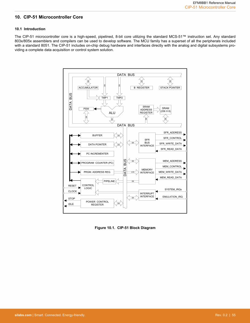
10. CIP-51 Microcontroller Core
10.1 Introduction
The CIP-51 microcontroller core is a high-speed, pipelined, 8-bit core utilizing the standard MCS-51™ instruction set. Any standard803x/805x assemblers and compilers can be used to develop software. The MCU family has a superset of all the peripherals includedwith a standard 8051. The CIP-51 includes on-chip debug hardware and interfaces directly with the analog and digital subsystems pro-viding a complete data acquisition or control system solution.
DATA BUS
TMP1 TMP2
PRGM. ADDRESS REG.
PC INCREMENTER
ALUPSW
DATA BUSD
ATA
BU
S
MEMORYINTERFACE
MEM_ADDRESSD8
PIPELINE
BUFFER
DATA POINTER
INTERRUPTINTERFACE
SYSTEM_IRQs
EMULATION_IRQ
MEM_CONTROL
CONTROLLOGIC
A16
PROGRAM COUNTER (PC)
STOP
CLOCK
RESET
IDLEPOWER CONTROL
REGISTER
DA
TA B
US
SFRBUS
INTERFACE
SFR_ADDRESS
SFR_CONTROL
SFR_WRITE_DATA
SFR_READ_DATA
D8
D8
B REGISTER
D8
D8
ACCUMULATORD
8
D8
D8
D8
D8
D8
D8
D8
MEM_WRITE_DATA
MEM_READ_DATA
D8
SRAMADDRESSREGISTER
SRAM(256 X 8)
D8
STACK POINTER
D8
Figure 10.1. CIP-51 Block Diagram
EFM8BB1 Reference ManualCIP-51 Microcontroller Core
silabs.com | Smart. Connected. Energy-friendly. Rev. 0.2 | 55

Performance
The CIP-51 employs a pipelined architecture that greatly increases its instruction throughput over the standard 8051 architecture. TheCIP-51 core executes 76 of its 109 instructions in one or two clock cycles, with no instructions taking more than eight clock cycles. Thetable below shows the distribution of instructions vs. the number of clock cycles required for execution.
Table 10.1. Instruction Execution Timing
Clocks toExecute
1 2 2 or 3 3 3 or 4 4 4 or 5 5 8
Number ofInstructions
26 50 5 14 7 3 1 2 1
Notes:1. Conditional branch instructions (indicated by "2 or 3", "3 or 4" and "4 or 5") require an extra clock cycle if the branch is taken.
10.2 Features
The CIP-51 Microcontroller core implements the standard 8051 organization and peripherals as well as additional custom peripheralsand functions to extend its capability. The CIP-51 includes the following features:• Fast, efficient, pipelined architecture.• Fully compatible with MCS-51 instruction set.• 0 to 25 MHz operating clock frequency.• 25 MIPS peak throughput with 25 MHz clock.• Extended interrupt handler.• Power management modes.• On-chip debug logic.• Program and data memory security.
10.3 Functional Description
10.3.1 Programming and Debugging Support
In-system programming of the flash program memory and communication with on-chip debug support logic is accomplished via the Sili-con Labs 2-Wire development interface (C2).
The on-chip debug support logic facilitates full speed in-circuit debugging, allowing the setting of hardware breakpoints, starting, stop-ping and single stepping through program execution (including interrupt service routines), examination of the program's call stack, andreading/writing the contents of registers and memory. This method of on-chip debugging is completely non-intrusive, requiring no RAM,stack, timers, or other on-chip resources.
The CIP-51 is supported by development tools from Silicon Labs and third party vendors. Silicon Labs provides an integrated develop-ment environment (IDE) including editor, debugger and programmer. The IDE's debugger and programmer interface to the CIP-51 viathe C2 interface to provide fast and efficient in-system device programming and debugging. Third party macro assemblers and C com-pilers are also available.
EFM8BB1 Reference ManualCIP-51 Microcontroller Core
silabs.com | Smart. Connected. Energy-friendly. Rev. 0.2 | 56

10.3.2 Instruction Set
The instruction set of the CIP-51 System Controller is fully compatible with the standard MCS-51™ instruction set. Standard 8051 de-velopment tools can be used to develop software for the CIP-51. All CIP-51 instructions are the binary and functional equivalent of theirMCS-51™ counterparts, including opcodes, addressing modes and effect on PSW flags. However, instruction timing is much fasterthan that of the standard 8051.
All instruction timing on the CIP-51 controller is based directly on the core clock timing. This is in contrast to many other 8-bit architec-tures, where a distinction is made between machine cycles and clock cycles, with machine cycles taking multiple core clock cycles.
Due to the pipelined architecture of the CIP-51, most instructions execute in the same number of clock cycles as there are programbytes in the instruction. Conditional branch instructions take one less clock cycle to complete when the branch is not taken as opposedto when the branch is taken. The following table summarizes the instruction set, including the mnemonic, number of bytes, and numberof clock cycles for each instruction.
Table 10.2. CIP-51 Instruction Set Summary
Mnemonic Description Bytes Clock Cycles
Arithmetic Operations
ADD A, Rn Add register to A 1 1
ADD A, direct Add direct byte to A 2 2
ADD A, @Ri Add indirect RAM to A 1 2
ADD A, #data Add immediate to A 2 2
ADDC A, Rn Add register to A with carry 1 1
ADDC A, direct Add direct byte to A with carry 2 2
ADDC A, @Ri Add indirect RAM to A with carry 1 2
ADDC A, #data Add immediate to A with carry 2 2
SUBB A, Rn Subtract register from A with borrow 1 1
SUBB A, direct Subtract direct byte from A with borrow 2 2
SUBB A, @Ri Subtract indirect RAM from A with borrow 1 2
SUBB A, #data Subtract immediate from A with borrow 2 2
INC A Increment A 1 1
INC Rn Increment register 1 1
INC direct Increment direct byte 2 2
INC @Ri Increment indirect RAM 1 2
DEC A Decrement A 1 1
DEC Rn Decrement register 1 1
DEC direct Decrement direct byte 2 2
DEC @Ri Decrement indirect RAM 1 2
INC DPTR Increment Data Pointer 1 1
MUL AB Multiply A and B 1 4
DIV AB Divide A by B 1 8
DA A Decimal adjust A 1 1
Logical Operations
ANL A, Rn AND Register to A 1 1
ANL A, direct AND direct byte to A 2 2
EFM8BB1 Reference ManualCIP-51 Microcontroller Core
silabs.com | Smart. Connected. Energy-friendly. Rev. 0.2 | 57
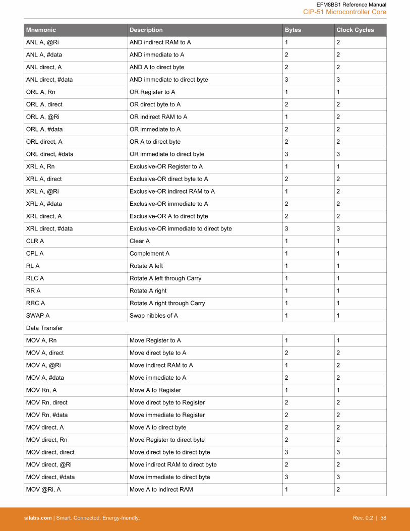
Mnemonic Description Bytes Clock Cycles
ANL A, @Ri AND indirect RAM to A 1 2
ANL A, #data AND immediate to A 2 2
ANL direct, A AND A to direct byte 2 2
ANL direct, #data AND immediate to direct byte 3 3
ORL A, Rn OR Register to A 1 1
ORL A, direct OR direct byte to A 2 2
ORL A, @Ri OR indirect RAM to A 1 2
ORL A, #data OR immediate to A 2 2
ORL direct, A OR A to direct byte 2 2
ORL direct, #data OR immediate to direct byte 3 3
XRL A, Rn Exclusive-OR Register to A 1 1
XRL A, direct Exclusive-OR direct byte to A 2 2
XRL A, @Ri Exclusive-OR indirect RAM to A 1 2
XRL A, #data Exclusive-OR immediate to A 2 2
XRL direct, A Exclusive-OR A to direct byte 2 2
XRL direct, #data Exclusive-OR immediate to direct byte 3 3
CLR A Clear A 1 1
CPL A Complement A 1 1
RL A Rotate A left 1 1
RLC A Rotate A left through Carry 1 1
RR A Rotate A right 1 1
RRC A Rotate A right through Carry 1 1
SWAP A Swap nibbles of A 1 1
Data Transfer
MOV A, Rn Move Register to A 1 1
MOV A, direct Move direct byte to A 2 2
MOV A, @Ri Move indirect RAM to A 1 2
MOV A, #data Move immediate to A 2 2
MOV Rn, A Move A to Register 1 1
MOV Rn, direct Move direct byte to Register 2 2
MOV Rn, #data Move immediate to Register 2 2
MOV direct, A Move A to direct byte 2 2
MOV direct, Rn Move Register to direct byte 2 2
MOV direct, direct Move direct byte to direct byte 3 3
MOV direct, @Ri Move indirect RAM to direct byte 2 2
MOV direct, #data Move immediate to direct byte 3 3
MOV @Ri, A Move A to indirect RAM 1 2
EFM8BB1 Reference ManualCIP-51 Microcontroller Core
silabs.com | Smart. Connected. Energy-friendly. Rev. 0.2 | 58

Mnemonic Description Bytes Clock Cycles
MOV @Ri, direct Move direct byte to indirect RAM 2 2
MOV @Ri, #data Move immediate to indirect RAM 2 2
MOV DPTR, #data16 Load DPTR with 16-bit constant 3 3
MOVC A, @A+DPTR Move code byte relative DPTR to A 1 3
MOVC A, @A+PC Move code byte relative PC to A 1 3
MOVX A, @Ri Move external data (8-bit address) to A 1 3
MOVX @Ri, A Move A to external data (8-bit address) 1 3
MOVX A, @DPTR Move external data (16-bit address) to A 1 3
MOVX @DPTR, A Move A to external data (16-bit address) 1 3
PUSH direct Push direct byte onto stack 2 2
POP direct Pop direct byte from stack 2 2
XCH A, Rn Exchange Register with A 1 1
XCH A, direct Exchange direct byte with A 2 2
XCH A, @Ri Exchange indirect RAM with A 1 2
XCHD A, @Ri Exchange low nibble of indirect RAM with A 1 2
Boolean Manipulation
CLR C Clear Carry 1 1
CLR bit Clear direct bit 2 2
SETB C Set Carry 1 1
SETB bit Set direct bit 2 2
CPL C Complement Carry 1 1
CPL bit Complement direct bit 2 2
ANL C, bit AND direct bit to Carry 2 2
ANL C, /bit AND complement of direct bit to Carry 2 2
ORL C, bit OR direct bit to carry 2 2
ORL C, /bit OR complement of direct bit to Carry 2 2
MOV C, bit Move direct bit to Carry 2 2
MOV bit, C Move Carry to direct bit 2 2
JC rel Jump if Carry is set 2 2 or 3
JNC rel Jump if Carry is not set 2 2 or 3
JB bit, rel Jump if direct bit is set 3 3 or 4
JNB bit, rel Jump if direct bit is not set 3 3 or 4
JBC bit, rel Jump if direct bit is set and clear bit 3 3 or 4
Program Branching
ACALL addr11 Absolute subroutine call 2 3
LCALL addr16 Long subroutine call 3 4
RET Return from subroutine 1 5
EFM8BB1 Reference ManualCIP-51 Microcontroller Core
silabs.com | Smart. Connected. Energy-friendly. Rev. 0.2 | 59

Mnemonic Description Bytes Clock Cycles
RETI Return from interrupt 1 5
AJMP addr11 Absolute jump 2 3
LJMP addr16 Long jump 3 4
SJMP rel Short jump (relative address) 2 3
JMP @A+DPTR Jump indirect relative to DPTR 1 3
JZ rel Jump if A equals zero 2 2 or 3
JNZ rel Jump if A does not equal zero 2 2 or 3
CJNE A, direct, rel Compare direct byte to A and jump if not equal 3 3 or 4
CJNE A, #data, rel Compare immediate to A and jump if not equal 3 3 or 4
CJNE Rn, #data, rel Compare immediate to Register and jump if not equal 3 3 or 4
CJNE @Ri, #data, rel Compare immediate to indirect and jump if not equal 3 4 or 5
DJNZ Rn, rel Decrement Register and jump if not zero 2 2 or 3
DJNZ direct, rel Decrement direct byte and jump if not zero 3 3 or 4
NOP No operation 1 1
Notes:• Rn: Register R0–R7 of the currently selected register bank.• @Ri: Data RAM location addressed indirectly through R0 or R1.• rel: 8-bit, signed (twos complement) offset relative to the first byte of the following instruction. Used by SJMP and all conditional
jumps.• direct: 8-bit internal data location’s address. This could be a direct-access Data RAM location (0x00–0x7F) or an SFR (0x80–
0xFF).• #data: 8-bit constant.• #data16: 16-bit constant.• bit: Direct-accessed bit in Data RAM or SFR.• addr11: 11-bit destination address used by ACALL and AJMP. The destination must be within the same 2 KB page of program
memory as the first byte of the following instruction.• addr16: 16-bit destination address used by LCALL and LJMP. The destination may be anywhere within the 8 KB program memory
space.• There is one unused opcode (0xA5) that performs the same function as NOP. All mnemonics copyrighted © Intel Corporation
1980.
10.4 CPU Core Registers
10.4.1 DPL: Data Pointer Low
Bit 7 6 5 4 3 2 1 0
Name DPL
Access RW
Reset 0x00
SFR Address: 0x82
Bit Name Reset Access Description
7:0 DPL 0x00 RW Data Pointer Low.
The DPL register is the low byte of the 16-bit DPTR. DPTR is used to access indirectly addressed flash memory or XRAM.
EFM8BB1 Reference ManualCIP-51 Microcontroller Core
silabs.com | Smart. Connected. Energy-friendly. Rev. 0.2 | 60
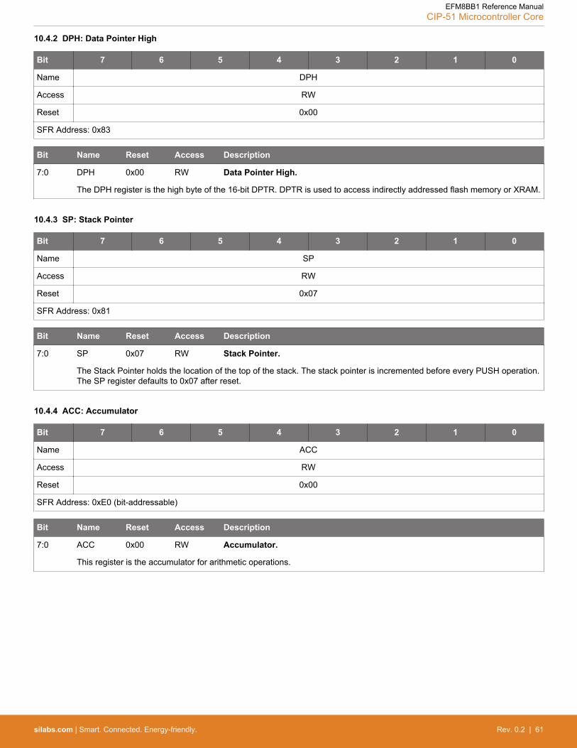
10.4.2 DPH: Data Pointer High
Bit 7 6 5 4 3 2 1 0
Name DPH
Access RW
Reset 0x00
SFR Address: 0x83
Bit Name Reset Access Description
7:0 DPH 0x00 RW Data Pointer High.
The DPH register is the high byte of the 16-bit DPTR. DPTR is used to access indirectly addressed flash memory or XRAM.
10.4.3 SP: Stack Pointer
Bit 7 6 5 4 3 2 1 0
Name SP
Access RW
Reset 0x07
SFR Address: 0x81
Bit Name Reset Access Description
7:0 SP 0x07 RW Stack Pointer.
The Stack Pointer holds the location of the top of the stack. The stack pointer is incremented before every PUSH operation.The SP register defaults to 0x07 after reset.
10.4.4 ACC: Accumulator
Bit 7 6 5 4 3 2 1 0
Name ACC
Access RW
Reset 0x00
SFR Address: 0xE0 (bit-addressable)
Bit Name Reset Access Description
7:0 ACC 0x00 RW Accumulator.
This register is the accumulator for arithmetic operations.
EFM8BB1 Reference ManualCIP-51 Microcontroller Core
silabs.com | Smart. Connected. Energy-friendly. Rev. 0.2 | 61

10.4.5 B: B Register
Bit 7 6 5 4 3 2 1 0
Name B
Access RW
Reset 0x00
SFR Address: 0xF0 (bit-addressable)
Bit Name Reset Access Description
7:0 B 0x00 RW B Register.
This register serves as a second accumulator for certain arithmetic operations.
EFM8BB1 Reference ManualCIP-51 Microcontroller Core
silabs.com | Smart. Connected. Energy-friendly. Rev. 0.2 | 62

10.4.6 PSW: Program Status Word
Bit 7 6 5 4 3 2 1 0
Name CY AC F0 RS OV F1 PARITY
Access RW RW RW RW RW RW R
Reset 0 0 0 0x0 0 0 0
SFR Address: 0xD0 (bit-addressable)
Bit Name Reset Access Description
7 CY 0 RW Carry Flag.
This bit is set when the last arithmetic operation resulted in a carry (addition) or a borrow (subtraction). It is cleared to logic0 by all other arithmetic operations.
6 AC 0 RW Auxiliary Carry Flag.
This bit is set when the last arithmetic operation resulted in a carry into (addition) or a borrow from (subtraction) the highorder nibble. It is cleared to logic 0 by all other arithmetic operations.
5 F0 0 RW User Flag 0.
This is a bit-addressable, general purpose flag for use under firmware control.
4:3 RS 0x0 RW Register Bank Select.
These bits select which register bank is used during register accesses.
Value Name Description
0x0 BANK0 Bank 0, Addresses 0x00-0x07
0x1 BANK1 Bank 1, Addresses 0x08-0x0F
0x2 BANK2 Bank 2, Addresses 0x10-0x17
0x3 BANK3 Bank 3, Addresses 0x18-0x1F
2 OV 0 RW Overflow Flag.
This bit is set to 1 under the following circumstances:
1. An ADD, ADDC, or SUBB instruction causes a sign-change overflow.
2. A MUL instruction results in an overflow (result is greater than 255).
3. A DIV instruction causes a divide-by-zero condition.
The OV bit is cleared to 0 by the ADD, ADDC, SUBB, MUL, and DIV instructions in all other cases.
1 F1 0 RW User Flag 1.
This is a bit-addressable, general purpose flag for use under firmware control.
0 PARITY 0 R Parity Flag.
This bit is set to logic 1 if the sum of the eight bits in the accumulator is odd and cleared if the sum is even.
EFM8BB1 Reference ManualCIP-51 Microcontroller Core
silabs.com | Smart. Connected. Energy-friendly. Rev. 0.2 | 63

11. Port I/O, Crossbar, External Interrupts, and Port Match
11.1 Introduction
Digital and analog resources are externally available on the device’s multi-purpose I/O pins. Port pins P0.0-P1.7 can be defined as gen-eral-purpose I/O (GPIO), assigned to one of the internal digital resources through the crossbar or dedicated channels, or assigned to ananalog function. Port pins P2.0 and P2.1 can be used as GPIO. Additionally, the C2 Interface Data signal (C2D) is shared with P2.0.
UART0
SPI0
SMB0
CMP0 Out
SYSCLK
PCA (CEXn)
Timer 0
CMP1 Out
Timer 1
Timer 2
2
4
2
2
2
1
3
PCA (ECI)1
1
1
1
CMP0 In
CMP1 In
INT0 / INT1
Port Match
P0, P1
P0
ADC0 InP0, P1
P1
P0, P1
P0
Priority Crossbar Decoder
P2.1P2.0
P1.6P1.5P1.4P1.3P1.2P1.1
P1.7
P1.0
P0.0 / VREFP0.1 / AGNDP0.2P0.3 / EXTCLKP0.4
P0.6 / CNVSTRP0.7
P0.5
PortControl
and Config
Figure 11.1. Port I/O Block Diagram
11.2 Features
• Up to 18 multi-functions I/O pins, supporting digital and analog functions.• Flexible priority crossbar decoder for digital peripheral assignment.• Two drive strength settings for each port.• Two direct-pin interrupt sources with dedicated interrupt vectors (INT0 and INT1).• Up to 16 direct-pin interrupt sources with shared interrupt vector (Port Match).
EFM8BB1 Reference ManualPort I/O, Crossbar, External Interrupts, and Port Match
silabs.com | Smart. Connected. Energy-friendly. Rev. 0.2 | 64

11.3 Functional Description
11.3.1 Port I/O Modes of Operation
Port pins are configured by firmware as digital or analog I/O using the special function registers. Port I/O initialization consists of thefollowing general steps:
1. Select the input mode (analog or digital) for all port pins, using the Port Input Mode register (PnMDIN).2. Select the output mode (open-drain or push-pull) for all port pins, using the Port Output Mode register (PnMDOUT).3. Select any pins to be skipped by the I/O crossbar using the Port Skip registers (PnSKIP).4. Assign port pins to desired peripherals.5. Enable the crossbar (XBARE = 1).
A diagram of the port I/O cell is shown in the following figure.
GND
VDD VDD
(WEAK)
PORT PAD
To/From Analog Peripheral
PxMDIN.x(1 for digital)(0 for analog)
Px.x – Output Logic Value(Port Latch or Crossbar)
XBARE(Crossbar Enable)
Px.x – Input Logic Value(Reads 0 when pin is configured as an analog I/O)
PxMDOUT.x(1 for push-pull)(0 for open-drain)
WEAKPUD(Weak Pull-Up Disable)
Figure 11.2. Port I/O Cell Block Diagram
Configuring Port Pins For Analog Modes
Any pins to be used for analog functions should be configured for analog mode. When a pin is configured for analog I/O, its weak pull-up, digital driver, and digital receiver are disabled. This saves power by eliminating crowbar current, and reduces noise on the analoginput. Pins configured as digital inputs may still be used by analog peripherals; however this practice is not recommended. Port pinsconfigured for analog functions will always read back a value of 0 in the corresponding Pn Port Latch register. To configure a pin asanalog, the following steps should be taken:
1. Clear the bit associated with the pin in the PnMDIN register to 0. This selects analog mode for the pin.2. Set the bit associated with the pin in the Pn register to 1.3. Skip the bit associated with the pin in the PnSKIP register to ensure the crossbar does not attempt to assign a function to the pin.
EFM8BB1 Reference ManualPort I/O, Crossbar, External Interrupts, and Port Match
silabs.com | Smart. Connected. Energy-friendly. Rev. 0.2 | 65
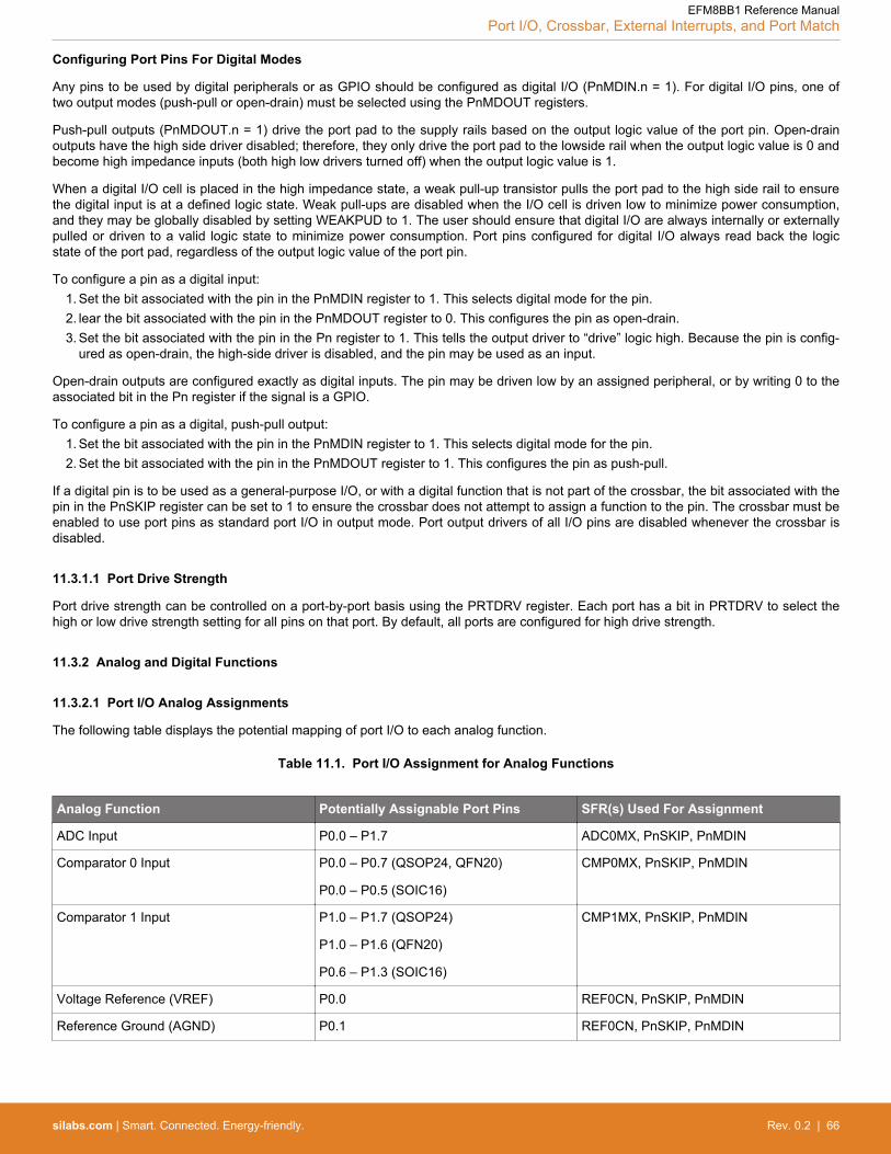
Configuring Port Pins For Digital Modes
Any pins to be used by digital peripherals or as GPIO should be configured as digital I/O (PnMDIN.n = 1). For digital I/O pins, one oftwo output modes (push-pull or open-drain) must be selected using the PnMDOUT registers.
Push-pull outputs (PnMDOUT.n = 1) drive the port pad to the supply rails based on the output logic value of the port pin. Open-drainoutputs have the high side driver disabled; therefore, they only drive the port pad to the lowside rail when the output logic value is 0 andbecome high impedance inputs (both high low drivers turned off) when the output logic value is 1.
When a digital I/O cell is placed in the high impedance state, a weak pull-up transistor pulls the port pad to the high side rail to ensurethe digital input is at a defined logic state. Weak pull-ups are disabled when the I/O cell is driven low to minimize power consumption,and they may be globally disabled by setting WEAKPUD to 1. The user should ensure that digital I/O are always internally or externallypulled or driven to a valid logic state to minimize power consumption. Port pins configured for digital I/O always read back the logicstate of the port pad, regardless of the output logic value of the port pin.
To configure a pin as a digital input:1. Set the bit associated with the pin in the PnMDIN register to 1. This selects digital mode for the pin.2. lear the bit associated with the pin in the PnMDOUT register to 0. This configures the pin as open-drain.3. Set the bit associated with the pin in the Pn register to 1. This tells the output driver to “drive” logic high. Because the pin is config-
ured as open-drain, the high-side driver is disabled, and the pin may be used as an input.
Open-drain outputs are configured exactly as digital inputs. The pin may be driven low by an assigned peripheral, or by writing 0 to theassociated bit in the Pn register if the signal is a GPIO.
To configure a pin as a digital, push-pull output:1. Set the bit associated with the pin in the PnMDIN register to 1. This selects digital mode for the pin.2. Set the bit associated with the pin in the PnMDOUT register to 1. This configures the pin as push-pull.
If a digital pin is to be used as a general-purpose I/O, or with a digital function that is not part of the crossbar, the bit associated with thepin in the PnSKIP register can be set to 1 to ensure the crossbar does not attempt to assign a function to the pin. The crossbar must beenabled to use port pins as standard port I/O in output mode. Port output drivers of all I/O pins are disabled whenever the crossbar isdisabled.
11.3.1.1 Port Drive Strength
Port drive strength can be controlled on a port-by-port basis using the PRTDRV register. Each port has a bit in PRTDRV to select thehigh or low drive strength setting for all pins on that port. By default, all ports are configured for high drive strength.
11.3.2 Analog and Digital Functions
11.3.2.1 Port I/O Analog Assignments
The following table displays the potential mapping of port I/O to each analog function.
Table 11.1. Port I/O Assignment for Analog Functions
Analog Function Potentially Assignable Port Pins SFR(s) Used For Assignment
ADC Input P0.0 – P1.7 ADC0MX, PnSKIP, PnMDIN
Comparator 0 Input P0.0 – P0.7 (QSOP24, QFN20)
P0.0 – P0.5 (SOIC16)
CMP0MX, PnSKIP, PnMDIN
Comparator 1 Input P1.0 – P1.7 (QSOP24)
P1.0 – P1.6 (QFN20)
P0.6 – P1.3 (SOIC16)
CMP1MX, PnSKIP, PnMDIN
Voltage Reference (VREF) P0.0 REF0CN, PnSKIP, PnMDIN
Reference Ground (AGND) P0.1 REF0CN, PnSKIP, PnMDIN
EFM8BB1 Reference ManualPort I/O, Crossbar, External Interrupts, and Port Match
silabs.com | Smart. Connected. Energy-friendly. Rev. 0.2 | 66

11.3.2.2 Port I/O Digital Assignments
The following table displays the potential mapping of port I/O to each digital function.
Table 11.2. Port I/O Assignment for Digital Functions
Digital Function Potentially Assignable Port Pins SFR(s) Used For Assignment
UART0, SPI0, SMB0, CP0, CP0A, CP1,CP1A, SYSCLK, PCA0 (CEX0-2 and ECI),T0, T1, T2
Any port pin available for assignment bythe crossbar. This includes P0.0 – P1.7pins which have their PnSKIP bit set to ‘0’.The crossbar will always assign UART0pins to P0.4 and P0.5.
XBR0, XBR1, XBR2
External Interrupt 0, External Interrupt 1 P0.0 – P0.7 IT01CF
Conversion Start (CNVSTR) P0.6 ADC0CN0
External Clock Input (EXTCLK) P0.3 CLKSEL
Port Match P0.0 – P1.7 P0MASK, P0MAT, P1MASK, P1MAT
Voltage Reference (VREF) P0.0 REF0CN, PnSKIP, PnMDIN
Any pin used for GPIO P0.0 – P2.1 P0SKIP, P1SKIP
EFM8BB1 Reference ManualPort I/O, Crossbar, External Interrupts, and Port Match
silabs.com | Smart. Connected. Energy-friendly. Rev. 0.2 | 67

11.3.3 Priority Crossbar Decoder
The priority crossbar decoder assigns a priority to each I/O function, starting at the top with UART0. The XBRn registers are used tocontrol which crossbar resources are assigned to physical I/O port pins.
When a digital resource is selected, the least-significant unassigned port pin is assigned to that resource (excluding UART0, which isalways assigned to dedicated pins). If a port pin is assigned, the crossbar skips that pin when assigning the next selected resource.Additionally, the the PnSKIP registers allow software to skip port pins that are to be used for analog functions, dedicated digital func-tions, or GPIO. If a port pin is to be used by a function which is not assigned through the crossbar, its corresponding PnSKIP bit shouldbe set to 1 in most cases. The crossbar skips these pins as if they were already assigned, and moves to the next unassigned pin.
It is possible for crossbar-assigned peripherals and dedicated functions to coexist on the same pin. For example, the port match func-tion could be configured to watch for a falling edge on a UART RX line and generate an interrupt or wake up the device from a low-power state. However, if two functions share the same pin, the crossbar will have control over the output characteristics of that pin andthe dedicated function will only have input access. Likewise, it is possible for firmware to read the logic state of any digital I/O pin as-signed to a crossbar peripheral, but the output state cannot be directly modified.
Figure 11.3 Crossbar Priority Decoder Example Assignments on page 68 shows an example of the resulting pin assignments of thedevice with UART0 and SPI0 enabled and P0.3 skipped (P0SKIP = 0x08). UART0 is the highest priority and it will be assigned first.The UART0 pins can only appear at fixed locations (in this example, P0.4 and P0.5), so it occupies those pins. The next-highest ena-bled peripheral is SPI0. P0.0, P0.1 and P0.2 are free, so SPI0 takes these three pins. The fourth pin, NSS, is routed to P0.6 becauseP0.3 is skipped and P0.4 and P0.5 are already occupied by the UART. Any other pins on the device are available for use as general-purpose digital I/O or analog functions.
UART0-TX
UART0-RX
0 1 2 3 4 5 6 7
P0Port
Pin Number
0 0 0 0 0 0 0
P0SKIPPin Skip Settings
SPI0-SCK
SPI0-MISO
SPI0-MOSI
SPI0-NSS
UART0 is assigned to fixed pins and has priority over SPI0.SPI0 is assigned to available, un-skipped pins.
Port pins assigned to the associated peripheral.
P0.3 is skipped by setting P0SKIP.3 to 1.
1
Figure 11.3. Crossbar Priority Decoder Example Assignments
EFM8BB1 Reference ManualPort I/O, Crossbar, External Interrupts, and Port Match
silabs.com | Smart. Connected. Energy-friendly. Rev. 0.2 | 68

11.3.3.1 Crossbar Functional Map
Figure 11.4 Full Crossbar Map on page 70 shows all of the potential peripheral-to-pin assignments available to the crossbar. Notethat this does not mean any peripheral can always be assigned to the highlighted pins. The actual pin assignments are determined bythe priority of the enabled peripherals.
EFM8BB1 Reference ManualPort I/O, Crossbar, External Interrupts, and Port Match
silabs.com | Smart. Connected. Energy-friendly. Rev. 0.2 | 69
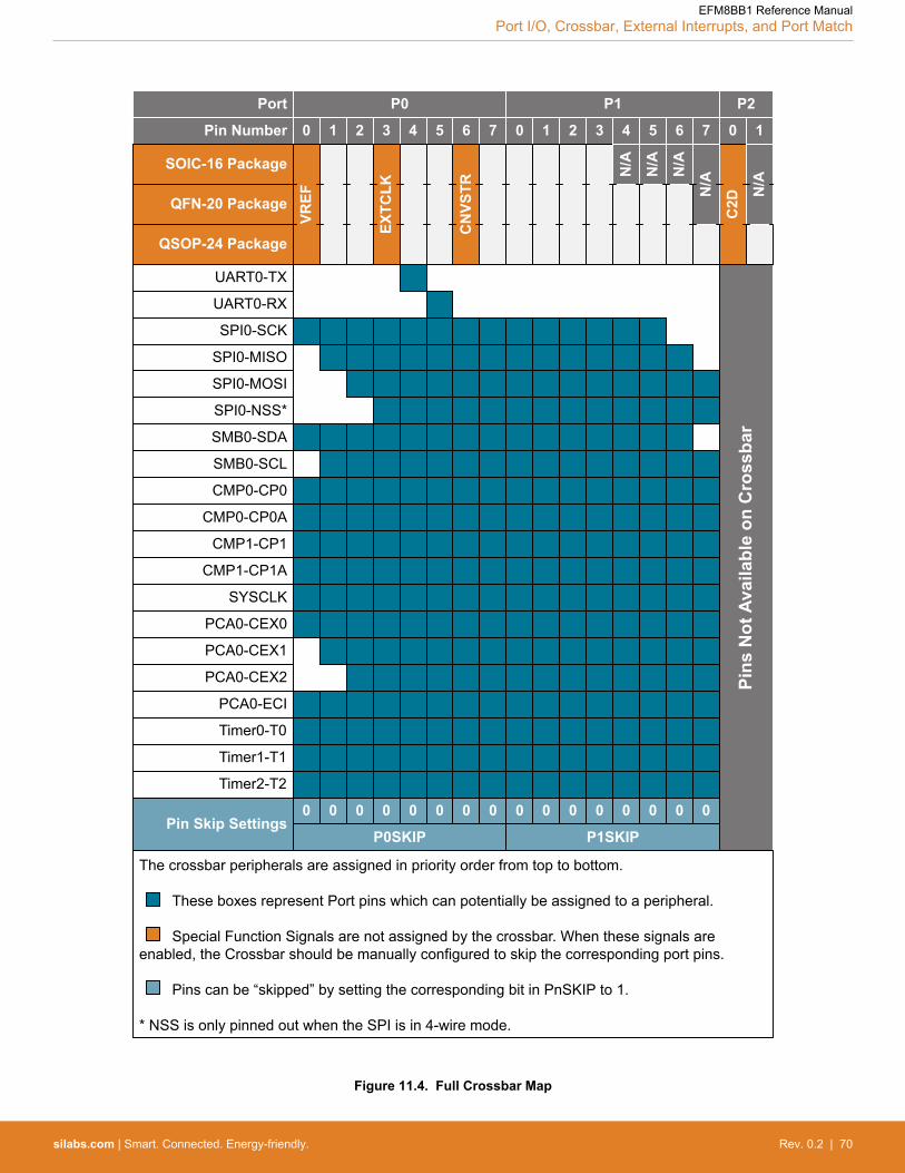
Pins
Not
Ava
ilabl
e on
Cro
ssba
r
UART0-TX
UART0-RX
SYSCLK
PCA0-CEX0
PCA0-CEX1
PCA0-CEX2
PCA0-ECI
Timer0-T0
Timer1-T1
0 1 2 3 4 5 6 7
P0Port
Pin Number
0 0 0 0 0 0 0 0
P0SKIPPin Skip Settings
SPI0-SCK
SPI0-MISO
SPI0-MOSI
SPI0-NSS*
0 1 2 3 4 5 6 7
P1
0 0 0 0 0 0 0 0
P1SKIP
0 1
P2
The crossbar peripherals are assigned in priority order from top to bottom.
These boxes represent Port pins which can potentially be assigned to a peripheral.
Special Function Signals are not assigned by the crossbar. When these signals are enabled, the Crossbar should be manually configured to skip the corresponding port pins.
Pins can be “skipped” by setting the corresponding bit in PnSKIP to 1.
* NSS is only pinned out when the SPI is in 4-wire mode.
SMB0-SDA
SMB0-SCL
QSOP-24 Package
VREF
EXTC
LK
CN
VSTR
C2DQFN-20 Package
Timer2-T2
CMP0-CP0
CMP0-CP0A
CMP1-CP1
CMP1-CP1A
N/A
SOIC-16 Package
N/AN
/A
N/A
N/A
Figure 11.4. Full Crossbar Map
EFM8BB1 Reference ManualPort I/O, Crossbar, External Interrupts, and Port Match
silabs.com | Smart. Connected. Energy-friendly. Rev. 0.2 | 70

11.3.4 INT0 and INT1
Two direct-pin digital interrupt sources (INT0 and INT1) are included, which can be routed to port 0 pins. Additional I/O interrupts areavailable through the port match function. As is the case on a standard 8051 architecture, certain controls for these two interrupt sour-ces are available in the Timer0/1 registers. Extensions to these controls which provide additional functionality are available in theIT01CF register. INT0 and INT1 are configurable as active high or low, edge- or level-sensitive. The IN0PL and IN1PL bits in theIT01CF register select active high or active low; the IT0 and IT1 bits in TCON select level- or edge-sensitive. The table below lists thepossible configurations.
Table 11.3. INT0/INT1 configuration
IT0 or IT1 IN0PL or IN1PL INT0 or INT1 Interrupt
1 0 Interrupt on falling edge
1 1 Interrupt on rising edge
0 0 Interrupt on low level
0 1 Interrupt on high level
INT0 and INT1 are assigned to port pins as defined in the IT01CF register. INT0 and INT1 port pin assignments are independent of anycrossbar assignments, and may be assigned to pins used by crossbar peripherals. INT0 and INT1 will monitor their assigned port pinswithout disturbing the peripheral that was assigned the port pin via the crossbar. To assign a port pin only to INT0 and/or INT1, config-ure the crossbar to skip the selected pin(s).
IE0 and IE1 in the TCON register serve as the interrupt-pending flags for the INT0 and INT1 external interrupts, respectively. If an INT0or INT1 external interrupt is configured as edge-sensitive, the corresponding interrupt pending flag is automatically cleared by the hard-ware when the CPU vectors to the ISR. When configured as level sensitive, the interrupt-pending flag remains logic 1 while the input isactive as defined by the corresponding polarity bit (IN0PL or IN1PL); the flag remains logic 0 while the input is inactive. The externalinterrupt source must hold the input active until the interrupt request is recognized. It must then deactivate the interrupt request beforeexecution of the ISR completes or another interrupt request will be generated.
11.3.5 Port Match
Port match functionality allows system events to be triggered by a logic value change on one or more port I/O pins. A software control-led value stored in the PnMATCH registers specifies the expected or normal logic values of the associated port pins (for example,P0MATCH.0 would correspond to P0.0). A port mismatch event occurs if the logic levels of the port’s input pins no longer match thesoftware controlled value. This allows software to be notified if a certain change or pattern occurs on the input pins regardless of theXBRn settings.
The PnMASK registers can be used to individually select which pins should be compared against the PnMATCH registers. A port mis-match event is generated if (Pn & PnMASK) does not equal (PnMATCH & PnMASK) for all ports with a PnMAT and PnMASK register.
A port mismatch event may be used to generate an interrupt or wake the device from low power modes. See the interrupts and poweroptions chapters for more details on interrupt and wake-up sources.
11.3.6 Direct Port I/O Access (Read/Write)
All port I/O are accessed through corresponding special function registers. When writing to a port, the value written to the SFR is latch-ed to maintain the output data value at each pin. When reading, the logic levels of the port's input pins are returned regardless of theXBRn settings (i.e., even when the pin is assigned to another signal by the crossbar, the port register can always read its correspondingport I/O pin). The exception to this is the execution of the read-modify-write instructions that target a Port Latch register as the destina-tion. The read-modify-write instructions when operating on a port SFR are the following: ANL, ORL, XRL, JBC, CPL, INC, DEC, DJNZand MOV, CLR or SETB, when the destination is an individual bit in a port SFR. For these instructions, the value of the latch register(not the pin) is read, modified, and written back to the SFR.
EFM8BB1 Reference ManualPort I/O, Crossbar, External Interrupts, and Port Match
silabs.com | Smart. Connected. Energy-friendly. Rev. 0.2 | 71
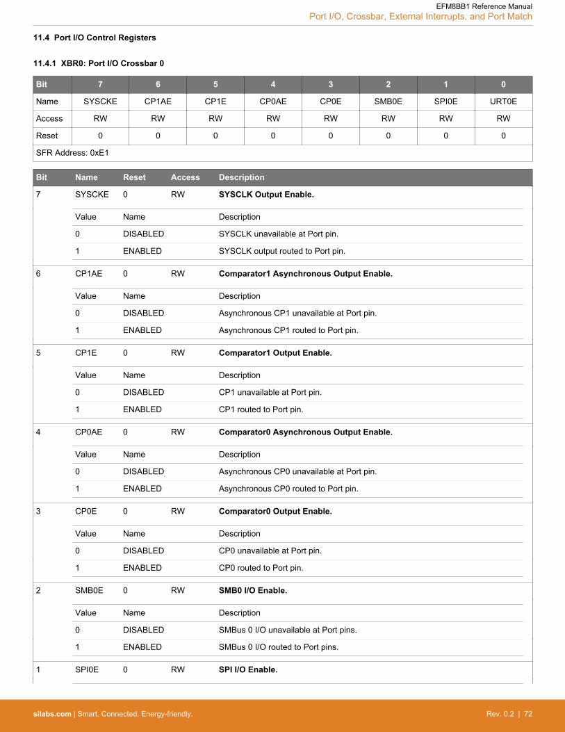
11.4 Port I/O Control Registers
11.4.1 XBR0: Port I/O Crossbar 0
Bit 7 6 5 4 3 2 1 0
Name SYSCKE CP1AE CP1E CP0AE CP0E SMB0E SPI0E URT0E
Access RW RW RW RW RW RW RW RW
Reset 0 0 0 0 0 0 0 0
SFR Address: 0xE1
Bit Name Reset Access Description
7 SYSCKE 0 RW SYSCLK Output Enable.
Value Name Description
0 DISABLED SYSCLK unavailable at Port pin.
1 ENABLED SYSCLK output routed to Port pin.
6 CP1AE 0 RW Comparator1 Asynchronous Output Enable.
Value Name Description
0 DISABLED Asynchronous CP1 unavailable at Port pin.
1 ENABLED Asynchronous CP1 routed to Port pin.
5 CP1E 0 RW Comparator1 Output Enable.
Value Name Description
0 DISABLED CP1 unavailable at Port pin.
1 ENABLED CP1 routed to Port pin.
4 CP0AE 0 RW Comparator0 Asynchronous Output Enable.
Value Name Description
0 DISABLED Asynchronous CP0 unavailable at Port pin.
1 ENABLED Asynchronous CP0 routed to Port pin.
3 CP0E 0 RW Comparator0 Output Enable.
Value Name Description
0 DISABLED CP0 unavailable at Port pin.
1 ENABLED CP0 routed to Port pin.
2 SMB0E 0 RW SMB0 I/O Enable.
Value Name Description
0 DISABLED SMBus 0 I/O unavailable at Port pins.
1 ENABLED SMBus 0 I/O routed to Port pins.
1 SPI0E 0 RW SPI I/O Enable.
EFM8BB1 Reference ManualPort I/O, Crossbar, External Interrupts, and Port Match
silabs.com | Smart. Connected. Energy-friendly. Rev. 0.2 | 72

Bit Name Reset Access Description
Value Name Description
0 DISABLED SPI I/O unavailable at Port pins.
1 ENABLED SPI I/O routed to Port pins. The SPI can be assigned either 3 or 4 GPIO pins.
0 URT0E 0 RW UART I/O Output Enable.
Value Name Description
0 DISABLED UART I/O unavailable at Port pin.
1 ENABLED UART TX, RX routed to Port pins P0.4 and P0.5.
EFM8BB1 Reference ManualPort I/O, Crossbar, External Interrupts, and Port Match
silabs.com | Smart. Connected. Energy-friendly. Rev. 0.2 | 73

11.4.2 XBR1: Port I/O Crossbar 1
Bit 7 6 5 4 3 2 1 0
Name Reserved T2E T1E T0E ECIE PCA0ME
Access R RW RW RW RW RW RW
Reset 0x0 0 0 0 0 0x0
SFR Address: 0xE2
Bit Name Reset Access Description
7:6 Reserved Must write reset value.
5 T2E 0 RW T2 Enable.
Value Name Description
0 DISABLED T2 unavailable at Port pin.
1 ENABLED T2 routed to Port pin.
4 T1E 0 RW T1 Enable.
Value Name Description
0 DISABLED T1 unavailable at Port pin.
1 ENABLED T1 routed to Port pin.
3 T0E 0 RW T0 Enable.
Value Name Description
0 DISABLED T0 unavailable at Port pin.
1 ENABLED T0 routed to Port pin.
2 ECIE 0 RW PCA0 External Counter Input Enable.
Value Name Description
0 DISABLED ECI unavailable at Port pin.
1 ENABLED ECI routed to Port pin.
1:0 PCA0ME 0x0 RW PCA Module I/O Enable.
Value Name Description
0x0 DISABLED All PCA I/O unavailable at Port pins.
0x1 CEX0 CEX0 routed to Port pin.
0x2 CEX0_CEX1 CEX0, CEX1 routed to Port pins.
0x3 CEX0_CEX1_CEX2 CEX0, CEX1, CEX2 routed to Port pins.
EFM8BB1 Reference ManualPort I/O, Crossbar, External Interrupts, and Port Match
silabs.com | Smart. Connected. Energy-friendly. Rev. 0.2 | 74

11.4.3 XBR2: Port I/O Crossbar 2
Bit 7 6 5 4 3 2 1 0
Name WEAKPUD XBARE Reserved
Access RW RW R
Reset 0 0 0x00
SFR Address: 0xE3
Bit Name Reset Access Description
7 WEAKPUD 0 RW Port I/O Weak Pullup Disable.
Value Name Description
0 PULL_UPS_ENABLED Weak Pullups enabled (except for Ports whose I/O are configured for analogmode).
1 PULL_UPS_DISABLED Weak Pullups disabled.
6 XBARE 0 RW Crossbar Enable.
Value Name Description
0 DISABLED Crossbar disabled.
1 ENABLED Crossbar enabled.
5:0 Reserved Must write reset value.
EFM8BB1 Reference ManualPort I/O, Crossbar, External Interrupts, and Port Match
silabs.com | Smart. Connected. Energy-friendly. Rev. 0.2 | 75

11.4.4 PRTDRV: Port Drive Strength
Bit 7 6 5 4 3 2 1 0
Name Reserved P2DRV P1DRV P0DRV
Access R RW RW RW
Reset 0x00 1 1 1
SFR Address: 0xF6
Bit Name Reset Access Description
7:3 Reserved Must write reset value.
2 P2DRV 1 RW Port 2 Drive Strength.
Value Name Description
0 LOW_DRIVE All pins on P2 use low drive strength.
1 HIGH_DRIVE All pins on P2 use high drive strength.
1 P1DRV 1 RW Port 1 Drive Strength.
Value Name Description
0 LOW_DRIVE All pins on P1 use low drive strength.
1 HIGH_DRIVE All pins on P1 use high drive strength.
0 P0DRV 1 RW Port 0 Drive Strength.
Value Name Description
0 LOW_DRIVE All pins on P0 use low drive strength.
1 HIGH_DRIVE All pins on P0 use high drive strength.
EFM8BB1 Reference ManualPort I/O, Crossbar, External Interrupts, and Port Match
silabs.com | Smart. Connected. Energy-friendly. Rev. 0.2 | 76

11.4.5 P0MASK: Port 0 Mask
Bit 7 6 5 4 3 2 1 0
Name B7 B6 B5 B4 B3 B2 B1 B0
Access RW RW RW RW RW RW RW RW
Reset 0 0 0 0 0 0 0 0
SFR Address: 0xFE
Bit Name Reset Access Description
7 B7 0 RW Port 0 Bit 7 Mask Value.
Value Name Description
0 IGNORED P0.7 pin logic value is ignored and will not cause a port mismatch event.
1 COMPARED P0.7 pin logic value is compared to P0MAT.7.
6 B6 0 RW Port 0 Bit 6 Mask Value.
See bit 7 description
5 B5 0 RW Port 0 Bit 5 Mask Value.
See bit 7 description
4 B4 0 RW Port 0 Bit 4 Mask Value.
See bit 7 description
3 B3 0 RW Port 0 Bit 3 Mask Value.
See bit 7 description
2 B2 0 RW Port 0 Bit 2 Mask Value.
See bit 7 description
1 B1 0 RW Port 0 Bit 1 Mask Value.
See bit 7 description
0 B0 0 RW Port 0 Bit 0 Mask Value.
See bit 7 description
EFM8BB1 Reference ManualPort I/O, Crossbar, External Interrupts, and Port Match
silabs.com | Smart. Connected. Energy-friendly. Rev. 0.2 | 77

11.4.6 P0MAT: Port 0 Match
Bit 7 6 5 4 3 2 1 0
Name B7 B6 B5 B4 B3 B2 B1 B0
Access RW RW RW RW RW RW RW RW
Reset 1 1 1 1 1 1 1 1
SFR Address: 0xFD
Bit Name Reset Access Description
7 B7 1 RW Port 0 Bit 7 Match Value.
Value Name Description
0 LOW P0.7 pin logic value is compared with logic LOW.
1 HIGH P0.7 pin logic value is compared with logic HIGH.
6 B6 1 RW Port 0 Bit 6 Match Value.
See bit 7 description
5 B5 1 RW Port 0 Bit 5 Match Value.
See bit 7 description
4 B4 1 RW Port 0 Bit 4 Match Value.
See bit 7 description
3 B3 1 RW Port 0 Bit 3 Match Value.
See bit 7 description
2 B2 1 RW Port 0 Bit 2 Match Value.
See bit 7 description
1 B1 1 RW Port 0 Bit 1 Match Value.
See bit 7 description
0 B0 1 RW Port 0 Bit 0 Match Value.
See bit 7 description
EFM8BB1 Reference ManualPort I/O, Crossbar, External Interrupts, and Port Match
silabs.com | Smart. Connected. Energy-friendly. Rev. 0.2 | 78

11.4.7 P0: Port 0 Pin Latch
Bit 7 6 5 4 3 2 1 0
Name B7 B6 B5 B4 B3 B2 B1 B0
Access RW RW RW RW RW RW RW RW
Reset 1 1 1 1 1 1 1 1
SFR Address: 0x80 (bit-addressable)
Bit Name Reset Access Description
7 B7 1 RW Port 0 Bit 7 Latch.
Value Name Description
0 LOW P0.7 is low. Set P0.7 to drive low.
1 HIGH P0.7 is high. Set P0.7 to drive or float high.
6 B6 1 RW Port 0 Bit 6 Latch.
See bit 7 description
5 B5 1 RW Port 0 Bit 5 Latch.
See bit 7 description
4 B4 1 RW Port 0 Bit 4 Latch.
See bit 7 description
3 B3 1 RW Port 0 Bit 3 Latch.
See bit 7 description
2 B2 1 RW Port 0 Bit 2 Latch.
See bit 7 description
1 B1 1 RW Port 0 Bit 1 Latch.
See bit 7 description
0 B0 1 RW Port 0 Bit 0 Latch.
See bit 7 description
Writing this register sets the port latch logic value for the associated I/O pins configured as digital I/O.
Reading this register returns the logic value at the pin, regardless if it is configured as output or input.
EFM8BB1 Reference ManualPort I/O, Crossbar, External Interrupts, and Port Match
silabs.com | Smart. Connected. Energy-friendly. Rev. 0.2 | 79
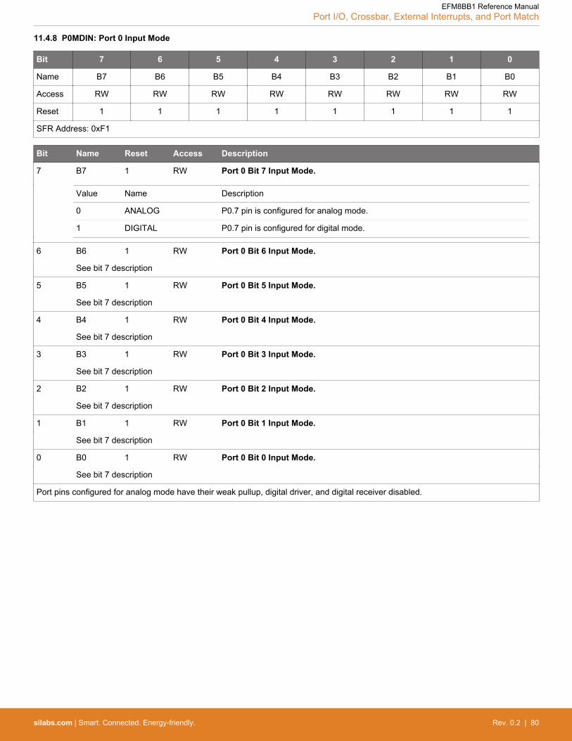
11.4.8 P0MDIN: Port 0 Input Mode
Bit 7 6 5 4 3 2 1 0
Name B7 B6 B5 B4 B3 B2 B1 B0
Access RW RW RW RW RW RW RW RW
Reset 1 1 1 1 1 1 1 1
SFR Address: 0xF1
Bit Name Reset Access Description
7 B7 1 RW Port 0 Bit 7 Input Mode.
Value Name Description
0 ANALOG P0.7 pin is configured for analog mode.
1 DIGITAL P0.7 pin is configured for digital mode.
6 B6 1 RW Port 0 Bit 6 Input Mode.
See bit 7 description
5 B5 1 RW Port 0 Bit 5 Input Mode.
See bit 7 description
4 B4 1 RW Port 0 Bit 4 Input Mode.
See bit 7 description
3 B3 1 RW Port 0 Bit 3 Input Mode.
See bit 7 description
2 B2 1 RW Port 0 Bit 2 Input Mode.
See bit 7 description
1 B1 1 RW Port 0 Bit 1 Input Mode.
See bit 7 description
0 B0 1 RW Port 0 Bit 0 Input Mode.
See bit 7 description
Port pins configured for analog mode have their weak pullup, digital driver, and digital receiver disabled.
EFM8BB1 Reference ManualPort I/O, Crossbar, External Interrupts, and Port Match
silabs.com | Smart. Connected. Energy-friendly. Rev. 0.2 | 80
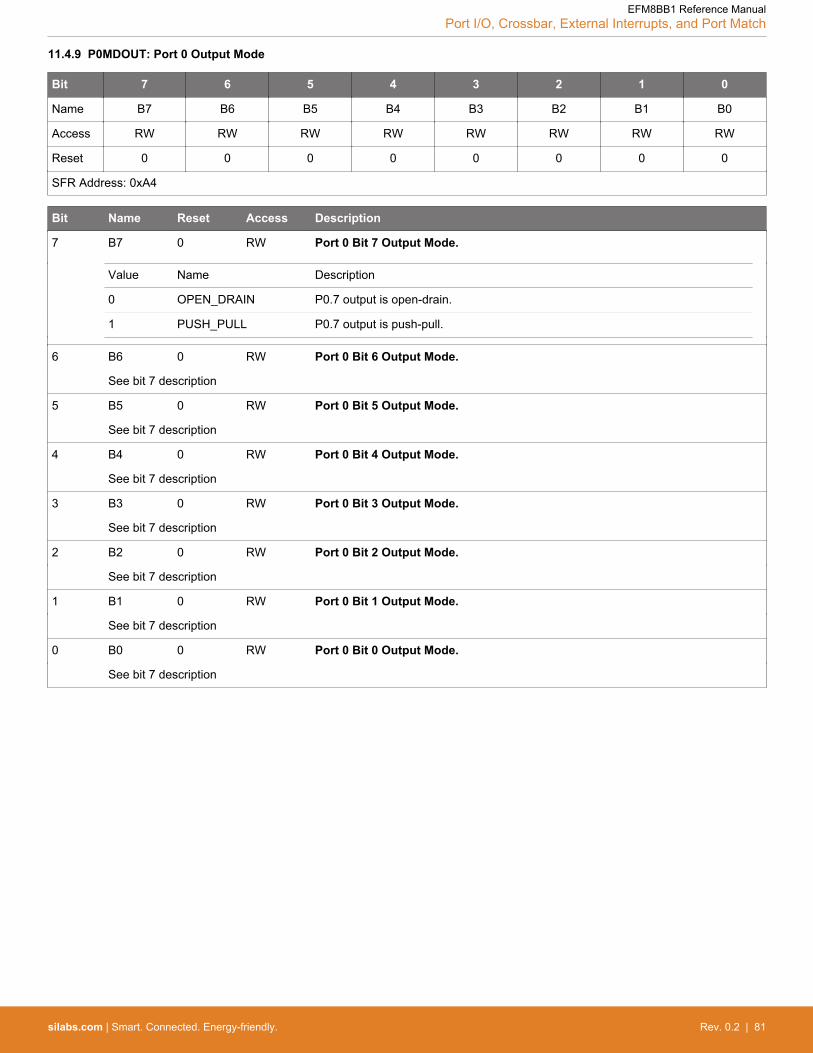
11.4.9 P0MDOUT: Port 0 Output Mode
Bit 7 6 5 4 3 2 1 0
Name B7 B6 B5 B4 B3 B2 B1 B0
Access RW RW RW RW RW RW RW RW
Reset 0 0 0 0 0 0 0 0
SFR Address: 0xA4
Bit Name Reset Access Description
7 B7 0 RW Port 0 Bit 7 Output Mode.
Value Name Description
0 OPEN_DRAIN P0.7 output is open-drain.
1 PUSH_PULL P0.7 output is push-pull.
6 B6 0 RW Port 0 Bit 6 Output Mode.
See bit 7 description
5 B5 0 RW Port 0 Bit 5 Output Mode.
See bit 7 description
4 B4 0 RW Port 0 Bit 4 Output Mode.
See bit 7 description
3 B3 0 RW Port 0 Bit 3 Output Mode.
See bit 7 description
2 B2 0 RW Port 0 Bit 2 Output Mode.
See bit 7 description
1 B1 0 RW Port 0 Bit 1 Output Mode.
See bit 7 description
0 B0 0 RW Port 0 Bit 0 Output Mode.
See bit 7 description
EFM8BB1 Reference ManualPort I/O, Crossbar, External Interrupts, and Port Match
silabs.com | Smart. Connected. Energy-friendly. Rev. 0.2 | 81

11.4.10 P0SKIP: Port 0 Skip
Bit 7 6 5 4 3 2 1 0
Name B7 B6 B5 B4 B3 B2 B1 B0
Access RW RW RW RW RW RW RW RW
Reset 0 0 0 0 0 0 0 0
SFR Address: 0xD4
Bit Name Reset Access Description
7 B7 0 RW Port 0 Bit 7 Skip.
Value Name Description
0 NOT_SKIPPED P0.7 pin is not skipped by the crossbar.
1 SKIPPED P0.7 pin is skipped by the crossbar.
6 B6 0 RW Port 0 Bit 6 Skip.
See bit 7 description
5 B5 0 RW Port 0 Bit 5 Skip.
See bit 7 description
4 B4 0 RW Port 0 Bit 4 Skip.
See bit 7 description
3 B3 0 RW Port 0 Bit 3 Skip.
See bit 7 description
2 B2 0 RW Port 0 Bit 2 Skip.
See bit 7 description
1 B1 0 RW Port 0 Bit 1 Skip.
See bit 7 description
0 B0 0 RW Port 0 Bit 0 Skip.
See bit 7 description
EFM8BB1 Reference ManualPort I/O, Crossbar, External Interrupts, and Port Match
silabs.com | Smart. Connected. Energy-friendly. Rev. 0.2 | 82

11.4.11 P1MASK: Port 1 Mask
Bit 7 6 5 4 3 2 1 0
Name B7 B6 B5 B4 B3 B2 B1 B0
Access RW RW RW RW RW RW RW RW
Reset 0 0 0 0 0 0 0 0
SFR Address: 0xEE
Bit Name Reset Access Description
7 B7 0 RW Port 1 Bit 7 Mask Value.
Value Name Description
0 IGNORED P1.7 pin logic value is ignored and will not cause a port mismatch event.
1 COMPARED P1.7 pin logic value is compared to P1MAT.7.
6 B6 0 RW Port 1 Bit 6 Mask Value.
See bit 7 description
5 B5 0 RW Port 1 Bit 5 Mask Value.
See bit 7 description
4 B4 0 RW Port 1 Bit 4 Mask Value.
See bit 7 description
3 B3 0 RW Port 1 Bit 3 Mask Value.
See bit 7 description
2 B2 0 RW Port 1 Bit 2 Mask Value.
See bit 7 description
1 B1 0 RW Port 1 Bit 1 Mask Value.
See bit 7 description
0 B0 0 RW Port 1 Bit 0 Mask Value.
See bit 7 description
Port 1 consists of 8 bits (P1.0-P1.7) on QSOP24 packages and 7 bits (P1.0-P1.6) on QFN20 packages and 4 bits (P1.0-P1.3) onSOIC16 packages.
EFM8BB1 Reference ManualPort I/O, Crossbar, External Interrupts, and Port Match
silabs.com | Smart. Connected. Energy-friendly. Rev. 0.2 | 83

11.4.12 P1MAT: Port 1 Match
Bit 7 6 5 4 3 2 1 0
Name B7 B6 B5 B4 B3 B2 B1 B0
Access RW RW RW RW RW RW RW RW
Reset 1 1 1 1 1 1 1 1
SFR Address: 0xED
Bit Name Reset Access Description
7 B7 1 RW Port 1 Bit 7 Match Value.
Value Name Description
0 LOW P1.7 pin logic value is compared with logic LOW.
1 HIGH P1.7 pin logic value is compared with logic HIGH.
6 B6 1 RW Port 1 Bit 6 Match Value.
See bit 7 description
5 B5 1 RW Port 1 Bit 5 Match Value.
See bit 7 description
4 B4 1 RW Port 1 Bit 4 Match Value.
See bit 7 description
3 B3 1 RW Port 1 Bit 3 Match Value.
See bit 7 description
2 B2 1 RW Port 1 Bit 2 Match Value.
See bit 7 description
1 B1 1 RW Port 1 Bit 1 Match Value.
See bit 7 description
0 B0 1 RW Port 1 Bit 0 Match Value.
See bit 7 description
Port 1 consists of 8 bits (P1.0-P1.7) on QSOP24 packages and 7 bits (P1.0-P1.6) on QFN20 packages and 4 bits (P1.0-P1.3) onSOIC16 packages.
EFM8BB1 Reference ManualPort I/O, Crossbar, External Interrupts, and Port Match
silabs.com | Smart. Connected. Energy-friendly. Rev. 0.2 | 84

11.4.13 P1: Port 1 Pin Latch
Bit 7 6 5 4 3 2 1 0
Name B7 B6 B5 B4 B3 B2 B1 B0
Access RW RW RW RW RW RW RW RW
Reset 1 1 1 1 1 1 1 1
SFR Address: 0x90 (bit-addressable)
Bit Name Reset Access Description
7 B7 1 RW Port 1 Bit 7 Latch.
Value Name Description
0 LOW P1.7 is low. Set P1.7 to drive low.
1 HIGH P1.7 is high. Set P1.7 to drive or float high.
6 B6 1 RW Port 1 Bit 6 Latch.
See bit 7 description
5 B5 1 RW Port 1 Bit 5 Latch.
See bit 7 description
4 B4 1 RW Port 1 Bit 4 Latch.
See bit 7 description
3 B3 1 RW Port 1 Bit 3 Latch.
See bit 7 description
2 B2 1 RW Port 1 Bit 2 Latch.
See bit 7 description
1 B1 1 RW Port 1 Bit 1 Latch.
See bit 7 description
0 B0 1 RW Port 1 Bit 0 Latch.
See bit 7 description
Writing this register sets the port latch logic value for the associated I/O pins configured as digital I/O.
Reading this register returns the logic value at the pin, regardless if it is configured as output or input.
Port 1 consists of 8 bits (P1.0-P1.7) on QSOP24 packages, 7 bits (P1.0-P1.6) on QFN20 packages, and 4 bits (P1.0-P1.3) on SOIC16packages.
EFM8BB1 Reference ManualPort I/O, Crossbar, External Interrupts, and Port Match
silabs.com | Smart. Connected. Energy-friendly. Rev. 0.2 | 85

11.4.14 P1MDIN: Port 1 Input Mode
Bit 7 6 5 4 3 2 1 0
Name B7 B6 B5 B4 B3 B2 B1 B0
Access RW RW RW RW RW RW RW RW
Reset 1 1 1 1 1 1 1 1
SFR Address: 0xF2
Bit Name Reset Access Description
7 B7 1 RW Port 1 Bit 7 Input Mode.
Value Name Description
0 ANALOG P1.7 pin is configured for analog mode.
1 DIGITAL P1.7 pin is configured for digital mode.
6 B6 1 RW Port 1 Bit 6 Input Mode.
See bit 7 description
5 B5 1 RW Port 1 Bit 5 Input Mode.
See bit 7 description
4 B4 1 RW Port 1 Bit 4 Input Mode.
See bit 7 description
3 B3 1 RW Port 1 Bit 3 Input Mode.
See bit 7 description
2 B2 1 RW Port 1 Bit 2 Input Mode.
See bit 7 description
1 B1 1 RW Port 1 Bit 1 Input Mode.
See bit 7 description
0 B0 1 RW Port 1 Bit 0 Input Mode.
See bit 7 description
Port pins configured for analog mode have their weak pullup, digital driver, and digital receiver disabled.
Port 1 consists of 8 bits (P1.0-P1.7) on QSOP24 packages, 7 bits (P1.0-P1.6) on QFN20 packages, and 4 bits (P1.0-P1.3) on SOIC16packages.
EFM8BB1 Reference ManualPort I/O, Crossbar, External Interrupts, and Port Match
silabs.com | Smart. Connected. Energy-friendly. Rev. 0.2 | 86

11.4.15 P1MDOUT: Port 1 Output Mode
Bit 7 6 5 4 3 2 1 0
Name B7 B6 B5 B4 B3 B2 B1 B0
Access RW RW RW RW RW RW RW RW
Reset 0 0 0 0 0 0 0 0
SFR Address: 0xA5
Bit Name Reset Access Description
7 B7 0 RW Port 1 Bit 7 Output Mode.
Value Name Description
0 OPEN_DRAIN P1.7 output is open-drain.
1 PUSH_PULL P1.7 output is push-pull.
6 B6 0 RW Port 1 Bit 6 Output Mode.
See bit 7 description
5 B5 0 RW Port 1 Bit 5 Output Mode.
See bit 7 description
4 B4 0 RW Port 1 Bit 4 Output Mode.
See bit 7 description
3 B3 0 RW Port 1 Bit 3 Output Mode.
See bit 7 description
2 B2 0 RW Port 1 Bit 2 Output Mode.
See bit 7 description
1 B1 0 RW Port 1 Bit 1 Output Mode.
See bit 7 description
0 B0 0 RW Port 1 Bit 0 Output Mode.
See bit 7 description
Port 1 consists of 8 bits (P1.0-P1.7) on QSOP24 packages, 7 bits (P1.0-P1.6) on QFN20 packages, and 4 bits (P1.0-P1.3) on SOIC16packages.
EFM8BB1 Reference ManualPort I/O, Crossbar, External Interrupts, and Port Match
silabs.com | Smart. Connected. Energy-friendly. Rev. 0.2 | 87

11.4.16 P1SKIP: Port 1 Skip
Bit 7 6 5 4 3 2 1 0
Name B7 B6 B5 B4 B3 B2 B1 B0
Access RW RW RW RW RW RW RW RW
Reset 0 0 0 0 0 0 0 0
SFR Address: 0xD5
Bit Name Reset Access Description
7 B7 0 RW Port 1 Bit 7 Skip.
Value Name Description
0 NOT_SKIPPED P1.7 pin is not skipped by the crossbar.
1 SKIPPED P1.7 pin is skipped by the crossbar.
6 B6 0 RW Port 1 Bit 6 Skip.
See bit 7 description
5 B5 0 RW Port 1 Bit 5 Skip.
See bit 7 description
4 B4 0 RW Port 1 Bit 4 Skip.
See bit 7 description
3 B3 0 RW Port 1 Bit 3 Skip.
See bit 7 description
2 B2 0 RW Port 1 Bit 2 Skip.
See bit 7 description
1 B1 0 RW Port 1 Bit 1 Skip.
See bit 7 description
0 B0 0 RW Port 1 Bit 0 Skip.
See bit 7 description
Port 1 consists of 8 bits (P1.0-P1.7) on QSOP24 packages, 7 bits (P1.0-P1.6) on QFN20 packages, and 4 bits (P1.0-P1.3) on SOIC16packages.
EFM8BB1 Reference ManualPort I/O, Crossbar, External Interrupts, and Port Match
silabs.com | Smart. Connected. Energy-friendly. Rev. 0.2 | 88

11.4.17 P2: Port 2 Pin Latch
Bit 7 6 5 4 3 2 1 0
Name Reserved B1 B0
Access R RW RW
Reset 0x01 1 1
SFR Address: 0xA0 (bit-addressable)
Bit Name Reset Access Description
7:2 Reserved Must write reset value.
1 B1 1 RW Port 2 Bit 1 Latch.
Value Name Description
0 LOW P2.1 is low. Set P2.1 to drive low.
1 HIGH P2.1 is high. Set P2.1 to drive or float high.
0 B0 1 RW Port 2 Bit 0 Latch.
See bit 1 description
Writing this register sets the port latch logic value for the associated I/O pins configured as digital I/O.
Reading this register returns the logic value at the pin, regardless if it is configured as output or input.
Port 2 consists of 2 bits (P2.0-P2.1) on QSOP24 devices and 1 bit (P2.0) on QFN20 and SOIC16 packages.
11.4.18 P2MDOUT: Port 2 Output Mode
Bit 7 6 5 4 3 2 1 0
Name Reserved B1 B0
Access R RW RW
Reset 0x00 0 0
SFR Address: 0xA6
Bit Name Reset Access Description
7:2 Reserved Must write reset value.
1 B1 0 RW Port 2 Bit 1 Output Mode.
Value Name Description
0 OPEN_DRAIN P2.1 output is open-drain.
1 PUSH_PULL P2.1 output is push-pull.
0 B0 0 RW Port 2 Bit 0 Output Mode.
See bit 1 description
Port 2 consists of 2 bits (P2.0-P2.1) on QSOP24 devices and 1 bit (P2.0) on QFN20 and SOIC16 packages.
EFM8BB1 Reference ManualPort I/O, Crossbar, External Interrupts, and Port Match
silabs.com | Smart. Connected. Energy-friendly. Rev. 0.2 | 89

11.5 INT0 and INT1 Control Registers
11.5.1 IT01CF: INT0/INT1 Configuration
Bit 7 6 5 4 3 2 1 0
Name IN1PL IN1SL IN0PL IN0SL
Access RW RW RW RW
Reset 0 0x0 0 0x1
SFR Address: 0xE4
Bit Name Reset Access Description
7 IN1PL 0 RW INT1 Polarity.
Value Name Description
0 ACTIVE_LOW INT1 input is active low.
1 ACTIVE_HIGH INT1 input is active high.
6:4 IN1SL 0x0 RW INT1 Port Pin Selection.
These bits select which port pin is assigned to INT1. This pin assignment is independent of the Crossbar; INT1 will monitorthe assigned port pin without disturbing the peripheral that has been assigned the port pin via the Crossbar. The Crossbarwill not assign the port pin to a peripheral if it is configured to skip the selected pin.
Value Name Description
0x0 P0_0 Select P0.0.
0x1 P0_1 Select P0.1.
0x2 P0_2 Select P0.2.
0x3 P0_3 Select P0.3.
0x4 P0_4 Select P0.4.
0x5 P0_5 Select P0.5.
0x6 P0_6 Select P0.6.
0x7 P0_7 Select P0.7.
3 IN0PL 0 RW INT0 Polarity.
Value Name Description
0 ACTIVE_LOW INT0 input is active low.
1 ACTIVE_HIGH INT0 input is active high.
2:0 IN0SL 0x1 RW INT0 Port Pin Selection.
These bits select which port pin is assigned to INT0. This pin assignment is independent of the Crossbar; INT0 will monitorthe assigned port pin without disturbing the peripheral that has been assigned the port pin via the Crossbar. The Crossbarwill not assign the port pin to a peripheral if it is configured to skip the selected pin.
Value Name Description
0x0 P0_0 Select P0.0.
0x1 P0_1 Select P0.1.
0x2 P0_2 Select P0.2.
EFM8BB1 Reference ManualPort I/O, Crossbar, External Interrupts, and Port Match
silabs.com | Smart. Connected. Energy-friendly. Rev. 0.2 | 90

Bit Name Reset Access Description
0x3 P0_3 Select P0.3.
0x4 P0_4 Select P0.4.
0x5 P0_5 Select P0.5.
0x6 P0_6 Select P0.6.
0x7 P0_7 Select P0.7.
EFM8BB1 Reference ManualPort I/O, Crossbar, External Interrupts, and Port Match
silabs.com | Smart. Connected. Energy-friendly. Rev. 0.2 | 91
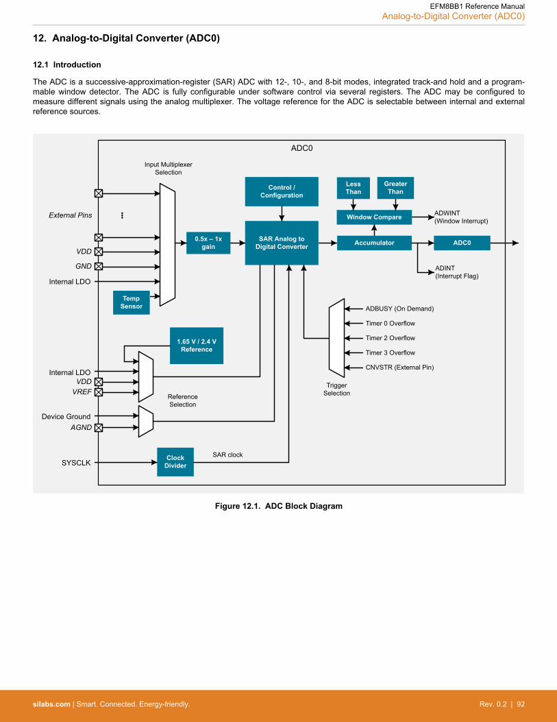
12. Analog-to-Digital Converter (ADC0)
12.1 Introduction
The ADC is a successive-approximation-register (SAR) ADC with 12-, 10-, and 8-bit modes, integrated track-and hold and a program-mable window detector. The ADC is fully configurable under software control via several registers. The ADC may be configured tomeasure different signals using the analog multiplexer. The voltage reference for the ADC is selectable between internal and externalreference sources.
ADC0
External Pins
SAR Analog to Digital Converter Accumulator
Window Compare
SYSCLKClock
Divider
Less Than
Greater Than
Device GroundAGND
0.5x – 1x gain
Control / Configuration
ADC0
VDDVREF
Internal LDO
1.65 V / 2.4 V Reference
Trigger Selection
ADWINT(Window Interrupt)
SAR clock
Temp Sensor
VDD
GND
Internal LDO
Input Multiplexer Selection
ADBUSY (On Demand)
Timer 0 Overflow
Timer 2 Overflow
Timer 3 Overflow
CNVSTR (External Pin)
ADINT(Interrupt Flag)
Reference Selection
Figure 12.1. ADC Block Diagram
EFM8BB1 Reference ManualAnalog-to-Digital Converter (ADC0)
silabs.com | Smart. Connected. Energy-friendly. Rev. 0.2 | 92

12.2 Features
• Up to 16 external inputs.• Single-ended 12-bit and 10-bit modes.• Supports an output update rate of 200 ksps samples per second in 12-bit mode or 800 ksps samples per second in 10-bit mode.• Operation in low power modes at lower conversion speeds.• Asynchronous hardware conversion trigger, selectable between software, external I/O and internal timer sources.• Output data window comparator allows automatic range checking.• Support for burst mode, which produces one set of accumulated data per conversion-start trigger with programmable power-on set-
tling and tracking time.• Conversion complete and window compare interrupts supported.• Flexible output data formatting.• Includes an internal fast-settling reference with two levels (1.65 V and 2.4 V) and support for external reference and signal ground.• Integrated temperature sensor.
12.3 Functional Description
12.3.1 Clocking
The ADC is clocked by an adjustable conversion clock (SARCLK). SARCLK is a divided version of the selected system clock whenburst mode is disabled (ADBMEN = 0), or a divided version of the HFOSC0 oscillator when burst mode is enabled (ADBMEN = 1). Theclock divide value is determined by the AD0SC field. In most applications, SARCLK should be adjusted to operate as fast as possible,without exceeding the maximum electrical specifications. The SARCLK does not directly determine sampling times or sampling rates.
12.3.2 Voltage Reference Options
The voltage reference multiplexer is configurable to use a number of different internal and external reference sources. The ground ref-erence mux allows the ground reference for ADC0 to be selected between the ground pin (GND) or a port pin dedicated to analogground (AGND). The voltage and ground reference options are configured using the REF0CN register. The REFSL field selects be-tween the different reference options, while GNDSL configures the ground connection.
12.3.2.1 Internal Voltage Reference
The high-speed internal reference offers two programmable voltage levels, and is self-contained and stabilized. It is not routed to anexternal pin and requires no external decoupling. When selected, the internal reference will be automatically enabled/disabled on an as-needed basis by the ADC. The reference can be set to one of two voltage values: 1.65 V or 2.4 V, depending on the value of theIREFLVL bit. The electrical specifications tables detail SAR clock and throughput limitations for each reference source.
12.3.2.2 Supply or LDO Voltage Reference
For applications with a non-varying power supply voltage, using the power supply as the voltage reference can provide the ADC withadded dynamic range at the cost of reduced power supply noise rejection. Additionally, the internal 1.8 V LDO supply to the core maybe used as a reference. Neither of these reference sources are routed to the VREF pin, and do not require additional external decou-pling.
12.3.2.3 External Voltage Reference
An external reference may be applied to the VREF pin. Bypass capacitors should be added as recommended by the manufacturer ofthe external voltage reference. If the manufacturer does not provide recommendations, a 4.7 µF in parallel with a 0.1 µF capacitor isrecommended.Note: The VREF pin is a multi-function GPIO pin. When using an external voltage reference, VREF should be configured as an analoginput and skipped by the crossbar.
EFM8BB1 Reference ManualAnalog-to-Digital Converter (ADC0)
silabs.com | Smart. Connected. Energy-friendly. Rev. 0.2 | 93
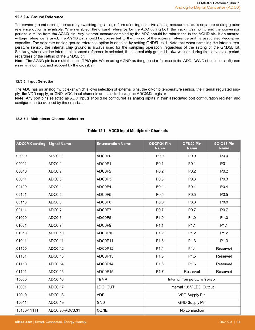
12.3.2.4 Ground Reference
To prevent ground noise generated by switching digital logic from affecting sensitive analog measurements, a separate analog groundreference option is available. When enabled, the ground reference for the ADC during both the tracking/sampling and the conversionperiods is taken from the AGND pin. Any external sensors sampled by the ADC should be referenced to the AGND pin. If an externalvoltage reference is used, the AGND pin should be connected to the ground of the external reference and its associated decouplingcapacitor. The separate analog ground reference option is enabled by setting GNDSL to 1. Note that when sampling the internal tem-perature sensor, the internal chip ground is always used for the sampling operation, regardless of the setting of the GNDSL bit.Similarly, whenever the internal high-speed reference is selected, the internal chip ground is always used during the conversion period,regardless of the setting of the GNDSL bit.Note: The AGND pin is a multi-function GPIO pin. When using AGND as the ground reference to the ADC, AGND should be configuredas an analog input and skipped by the crossbar.
12.3.3 Input Selection
The ADC has an analog multiplexer which allows selection of external pins, the on-chip temperature sensor, the internal regulated sup-ply, the VDD supply, or GND. ADC input channels are selected using the ADC0MX register.Note: Any port pins selected as ADC inputs should be configured as analog inputs in their associated port configuration register, andconfigured to be skipped by the crossbar.
12.3.3.1 Multiplexer Channel Selection
Table 12.1. ADC0 Input Multiplexer Channels
ADC0MX setting Signal Name Enumeration Name QSOP24 PinName
QFN20 PinName
SOIC16 PinName
00000 ADC0.0 ADC0P0 P0.0 P0.0 P0.0
00001 ADC0.1 ADC0P1 P0.1 P0.1 P0.1
00010 ADC0.2 ADC0P2 P0.2 P0.2 P0.2
00011 ADC0.3 ADC0P3 P0.3 P0.3 P0.3
00100 ADC0.4 ADC0P4 P0.4 P0.4 P0.4
00101 ADC0.5 ADC0P5 P0.5 P0.5 P0.5
00110 ADC0.6 ADC0P6 P0.6 P0.6 P0.6
00111 ADC0.7 ADC0P7 P0.7 P0.7 P0.7
01000 ADC0.8 ADC0P8 P1.0 P1.0 P1.0
01001 ADC0.9 ADC0P9 P1.1 P1.1 P1.1
01010 ADC0.10 ADC0P10 P1.2 P1.2 P1.2
01011 ADC0.11 ADC0P11 P1.3 P1.3 P1.3
01100 ADC0.12 ADC0P12 P1.4 P1.4 Reserved
01101 ADC0.13 ADC0P13 P1.5 P1.5 Reserved
01110 ADC0.14 ADC0P14 P1.6 P1.6 Reserved
01111 ADC0.15 ADC0P15 P1.7 Reserved Reserved
10000 ADC0.16 TEMP Internal Temperature Sensor
10001 ADC0.17 LDO_OUT Internal 1.8 V LDO Output
10010 ADC0.18 VDD VDD Supply Pin
10011 ADC0.19 GND GND Supply Pin
10100-11111 ADC0.20-ADC0.31 NONE No connection
EFM8BB1 Reference ManualAnalog-to-Digital Converter (ADC0)
silabs.com | Smart. Connected. Energy-friendly. Rev. 0.2 | 94

12.3.4 Gain Setting
The ADC has gain settings of 1x and 0.5x. In 1x mode, the full scale reading of the ADC is determined directly by VREF. In 0.5x mode,the full-scale reading of the ADC occurs when the input voltage is VREF x 2. The 0.5x gain setting can be useful to obtain a higher inputvoltage range when using a small VREF voltage, or to measure input voltages that are between VREF and the supply voltage. Gainsettings for the ADC are controlled by the ADGN bit in register ADC0CF. Note that even with a gain setting of 0.5, voltages above thesupply rail cannot be measured directly by the ADC.
12.3.5 Initiating Conversions
A conversion can be initiated in many ways, depending on the programmed state of the ADCM bitfield. Conversions may be initiated byone of the following:
1. Software-triggered—Writing a 1 to the ADBUSY bit initiates the conversion.2. Hardware-triggered—An automatic internal event such as a timer overflow initiates the conversion.3. External pin-triggered—A rising edge on the CNVSTR input signal initiates the conversion.
Writing a 1 to ADBUSY provides software control of ADC0 whereby conversions are performed "on-demand". All other trigger sourcesoccur autonomous to code execution. When the conversion is complete, the ADC posts the result to its output register and sets theADC interrupt flag (ADINT). ADINT may be used to trigger a system interrupts, if enabled, or polled by firmware.
During a conversion, the ADBUSY bit is set to logic 1 and reset to logic 0 when the conversion is complete. However, the ADBUSY bitshould not be used to poll for ADC conversion completion. The ADC0 interrupt flag (ADINT) should be used instead of the ADBUSY bit.Converted data is available in the ADC0 data registers, ADC0H:ADC0L, when the conversion is complete.Note: The CNVSTR pin is a multi-function GPIO pin. When the CNVSTR input is used as the ADC conversion source, the associatedport pin should be skipped in the crossbar settings.
12.3.6 Input Tracking
Each ADC conversion must be preceded by a minimum tracking time to allow the voltage on the sampling capacitor to settle, and forthe converted result to be accurate.
EFM8BB1 Reference ManualAnalog-to-Digital Converter (ADC0)
silabs.com | Smart. Connected. Energy-friendly. Rev. 0.2 | 95

Settling Time Requirements
The absolute minimum tracking time is given in the electrical specifications tables. It may be necessary to track for longer than the mini-mum tracking time specification, depending on the application. For example, if the ADC input is presented with a large series impe-dance, it will take longer for the sampling cap to settle on the final value during the tracking phase. The exact amount of tracking timerequired is a function of all series impedance (including the internal mux impedance and any external impedance sources), the sam-pling capacitance, and the desired accuracy.
RMUX
CSAMPLE
RCInput= RMUX * CSAMPLE
MUX Select
Input Channel
Note: The value of CSAMPLE depends on the PGA gain. See the electrical specifications for details.
Figure 12.2. ADC Eqivalent Input Circuit
The required ADC0 settling time for a given settling accuracy (SA) may be approximated as follows:
t = ln ( 2n
SA ) x RTOTAL x CSAMPLE
Where: SA is the settling accuracy, given as a fraction of an LSB (for example, 0.25 to settle within 1/4 LSB)
t is the required settling time in seconds
RTOTAL is the sum of the ADC mux resistance and any external source resistance.
CSAMPLE is the size of the ADC sampling capacitor.
n is the ADC resolution in bits.
When measuring any internal source, RTOTAL reduces to RMUX. See the electrical specification tables in the datasheet for ADC mini-mum settling time requirements as well as the mux impedance and sampling capacitor values.
EFM8BB1 Reference ManualAnalog-to-Digital Converter (ADC0)
silabs.com | Smart. Connected. Energy-friendly. Rev. 0.2 | 96

Configuring the Tracking Time
When burst mode is disabled, the ADTM bit controls the ADC track-and-hold mode. In its default state the ADC input is continuouslytracked, except when a conversion is in progress. A conversion will begin immediately when the start-of-conversion trigger occurs.When the ADTM bit is logic 1, each conversion is preceded by a tracking period of 4 SAR clocks (after the start-of-conversion signal)for any internal conversion trigger source. When the CNVSTR signal is used to initiate conversions with ADTM set to 1, ADC0 tracksonly when CNVSTR is low; conversion begins on the rising edge of CNVSTR. Setting ADTM to 1 is primarily useful when AMUX set-tings are frequently changed and conversions are started using the ADBUSY bit.
Write '1' to ADBUSY,Timer Overflow
ADTM = 1 Track Convert Low Power Mode
ADTM = 0Track or Convert Convert Track
Low Power or Convert
SAR Clocks
SAR Clocks
B. ADC0 Timing for Internal Trigger Source
1 2 3 4 5 6 7 8 9
CNVSTR
ADTM = 1
A. ADC0 Timing for External Trigger Source
SAR Clocks
Track or Convert Convert TrackADTM = 0
Track Convert Low Power Mode
Low Power or Convert
10 11 12 13 14
1 2 3 4 5 6 7 8 9 10 11 12 13 14
1 2 3 4 5 6 7 8 9 10 11 12 13 14 15 16 17 18
Figure 12.3. Track and Conversion Example Timing (Normal, Non-Burst Operation)
When burst mode is enabled, additional tracking times may need to be specified. Because burst mode may power the ADC on from anunpowered state and take multiple conversions for each start-of-conversion source, two additional timing fields are provided. If the ADCis powered down when the burst sequence begins, it will automatically power up and wait for the time specified in the ADPWR bit field.If the ADC is already powered on, tracking depends solely on ADTM for the first conversion. The ADTK field determines the amount oftracking time given to any subsequent samples in burst mode—essentially, ADTK specifies how long the ADC will wait between burt-mode conversions. If ADTM is set, an additional 4 SAR clocks will be added to the tracking phase of all conversions in burst mode.
EFM8BB1 Reference ManualAnalog-to-Digital Converter (ADC0)
silabs.com | Smart. Connected. Energy-friendly. Rev. 0.2 | 97

Figure 12.4. Burst Mode Timing
Convert Start
ADTM = 1ADEN = 0
PoweredDown
Powered Down
T4 CPower-Up
and Track T C T C T C Power-Upand Track T C..
ADTM = 0ADEN = 0
PoweredDown
Powered DownCPower-Up
and Track T C T C T C Power-Upand Track T C..
ADPWR
T = Tracking set by ADTKT4 = Tracking set by ADTM (4 SAR clocks)C = Converting
ADTK
T4
T4
T4
12.3.7 Burst Mode
Burst mode is a power saving feature that allows the ADC to remain in a low power state between conversions. When burst mode isenabled, the ADC wakes from a low power state, accumulates 1, 4, 8, 16, 32, or 64 samples using the internal low-power high-frequen-cy oscillator, then re-enters a low power state. Since the burst mode clock is independent of the system clock, the ADC can performmultiple conversions then enter a low power state within a single system clock cycle, even if the system clock is running from a slowoscillator.Note: When using burst mode, care must be taken to issue a convert start signal no faster than once every four SYSCLK periods. Thisincludes external convert start signals. The ADC will ignore convert start signals which arrive before a burst is finished.
Burst mode is enabled by setting ADBMEN to logic 1. When in burst mode, ADEN controls the ADC idle power state (i.e., the state theADC enters when not tracking or performing conversions). If ADEN is set to logic 0, the ADC is powered down after each burst. If AD-EN is set to logic 1, the ADC remains enabled after each burst. On each convert start signal, the ADC is awakened from its idle powerstate. If the ADC is powered down, it will automatically power up and wait for the amount of time programmed to the ADPWR bits be-fore performing a conversion. Otherwise, the ADC will start tracking and converting immediately.
When burst mode is enabled, a single convert start will initiate a number of conversions equal to the repeat count. When burst mode isdisabled, a convert start is required to initiate each conversion. In both modes, the ADC end of conversion interrupt flag (ADINT) will beset after “repeat count” conversions have been accumulated. Similarly, the window comparator will not compare the result to the great-er-than and less-than registers until “repeat count” conversions have been accumulated.
12.3.8 8-Bit Mode
Setting the AD8BE bit to 1 will put the ADC in 8-bit mode. In 8-bit mode, only the 8 MSBs of data are converted, allowing the conversionto be completed in fewer SAR clock cycles than a 10-bit conversion. The two LSBs of a conversion are always 00 in this mode, and theADC0L register will always read back 0x00.
EFM8BB1 Reference ManualAnalog-to-Digital Converter (ADC0)
silabs.com | Smart. Connected. Energy-friendly. Rev. 0.2 | 98

12.3.9 12-Bit Mode
When configured for 12-bit conversions, the ADC performs four 10-bit conversions using four different reference voltages and combinesthe results into a single 12-bit value. Unlike simple averaging techniques, this method provides true 12-bit resolution of ac or dc inputsignals without depending on noise to provide dithering. The converter also employs a hardware dynamic element matching algorithmthat reconfigures the largest elements of the internal DAC for each of the four 10-bit conversions. This reconfiguration cancels anymatching errors and enables the converter to achieve 12-bit linearity performance to go along with its 12-bit resolution.
The 12-bit mode is enabled by setting the AD12BE bit in register ADC0AC to logic 1 and configuring the ADC in burst mode (ADBMEN= 1) for four or more conversions. The conversion can be initiated using any of the conversion start sources, and the 12-bit result willappear in the ADC0H and ADC0L registers. Since the 12-bit result is formed from a combination of four 10-bit results, the maximumoutput value is 4 x (1023) = 4092, rather than the max value of (2^12 – 1) = 4095 that is produced by a traditional 12-bit converter. Tofurther increase resolution, the burst mode repeat value may be configured to any multiple of four conversions. For example, if a repeatvalue of 16 is selected, the ADC0 output will be a 14-bit number (sum of four 12-bit numbers) with 13 effective bits of resolution.
The AD12SM bit in register ADC0TK controls when the ADC will track and sample the input signal. When AD12SM is set to 1, theselected input signal will be tracked before the first conversion of a set and held internally during all four conversions. When AD12SM iscleared to 0, the ADC will track and sample the selected input before each of the four conversions in a set. When maximum throughput(180-200 ksps) is needed, it is recommended that AD12SM be set to 1 and ADTK to 0x3F, and that the ADC be placed in always-onmode (ADEN = 1). For sample rates under 180 ksps, or when accumulating multiple samples, AD12SM should normally be cleared to0, and ADTK should be configured to provide the appropriate settling time for the subsequent conversions.
EFM8BB1 Reference ManualAnalog-to-Digital Converter (ADC0)
silabs.com | Smart. Connected. Energy-friendly. Rev. 0.2 | 99

12.3.10 Output Formatting
The registers ADC0H and ADC0L contain the high and low bytes of the output conversion code from the ADC at the completion of eachconversion. Data can be right-justified or left-justified, depending on the setting of the ADSJST field. When the repeat count is set to 1in 10-bit mode, conversion codes are represented as 10-bit unsigned integers. Inputs are measured from 0 to VREF x 1023/1024. Ex-ample codes are shown below for both right-justified and left-justified data. Unused bits in the ADC0H and ADC0L registers are set to 0.
Table 12.2. 10-Bit Output Code Example
Input Voltage Right-Justified (ADSJST = 000)
ADC0H:L
Left-Justified (ADSJST = 100)
ADC0H:L
VREF x 1023/1024 0x03FF 0xFFC0
VREF x 512/1024 0x0200 0x8000
VREF x 256/1024 0x0100 0x4000
0 0x0000 0x0000
When the repeat count is greater than 1, the output conversion code represents the accumulated result of the conversions performedand is updated after the last conversion in the series is finished. Sets of 4, 8, 16, 32, or 64 consecutive samples can be accumulatedand represented in unsigned integer format. The repeat count can be selected using the ADRPT bit field. When a repeat count is higherthan 1, the ADC output must be right-justified (ADSJST = 0xx); unused bits in the ADC0H and ADC0L registers are set to 0. The exam-ple below shows the right-justified result for various input voltages and repeat counts. Notice that accumulating 2n samples is equiva-lent to left-shifting by n bit positions when all samples returned from the ADC have the same value.
Table 12.3. Effects of ADRPT on Output Code
Input Voltage Repeat Count = 4 Repeat Count = 16 Repeat Count = 64
VREF x 1023/1024 0x0FFC 0x3FF0 0xFFC0
VREF x 512/1024 0x0800 0x2000 0x8000
VREF x 511/1024 0x07FC 0x1FF0 0x7FC0
0 0x0000 0x0000 0x0000
Additionally, the ADSJST bit field can be used to format the contents of the 16-bit accumulator. The accumulated result can be shiftedright by 1, 2, or 3 bit positions. Based on the principles of oversampling and averaging, the effective ADC resolution increases by 1 biteach time the oversampling rate is increased by a factor of 4. The example below shows how to increase the effective ADC resolutionby 1, 2, and 3 bits to obtain an effective ADC resolution of 11- bit, 12-bit, or 13-bit respectively without CPU intervention.
Table 12.4. Using ADSJST for Output Formatting
Input Voltage Repeat Count = 4
Shift Right = 1
11-Bit Result
Repeat Count = 16
Shift Right = 2
12-Bit Result
Repeat Count = 64
Shift Right = 3
12-Bit Result
VREF x 1023/1024 0x07F7 0x0FFC 0x1FF8
VREF x 512/1024 0x0400 0x0800 0x1000
VREF x 511/1024 0x03FE 0x04FC 0x0FF8
0 0x0000 0x0000 0x0000
EFM8BB1 Reference ManualAnalog-to-Digital Converter (ADC0)
silabs.com | Smart. Connected. Energy-friendly. Rev. 0.2 | 100
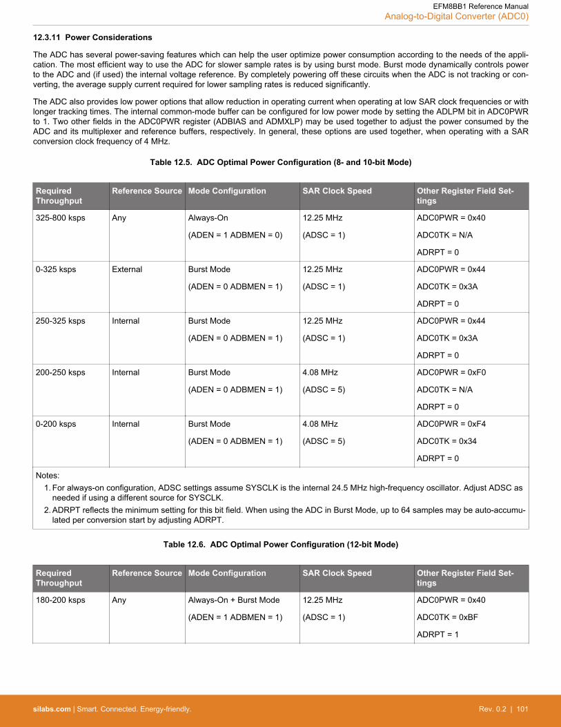
12.3.11 Power Considerations
The ADC has several power-saving features which can help the user optimize power consumption according to the needs of the appli-cation. The most efficient way to use the ADC for slower sample rates is by using burst mode. Burst mode dynamically controls powerto the ADC and (if used) the internal voltage reference. By completely powering off these circuits when the ADC is not tracking or con-verting, the average supply current required for lower sampling rates is reduced significantly.
The ADC also provides low power options that allow reduction in operating current when operating at low SAR clock frequencies or withlonger tracking times. The internal common-mode buffer can be configured for low power mode by setting the ADLPM bit in ADC0PWRto 1. Two other fields in the ADC0PWR register (ADBIAS and ADMXLP) may be used together to adjust the power consumed by theADC and its multiplexer and reference buffers, respectively. In general, these options are used together, when operating with a SARconversion clock frequency of 4 MHz.
Table 12.5. ADC Optimal Power Configuration (8- and 10-bit Mode)
RequiredThroughput
Reference Source Mode Configuration SAR Clock Speed Other Register Field Set-tings
325-800 ksps Any Always-On
(ADEN = 1 ADBMEN = 0)
12.25 MHz
(ADSC = 1)
ADC0PWR = 0x40
ADC0TK = N/A
ADRPT = 0
0-325 ksps External Burst Mode
(ADEN = 0 ADBMEN = 1)
12.25 MHz
(ADSC = 1)
ADC0PWR = 0x44
ADC0TK = 0x3A
ADRPT = 0
250-325 ksps Internal Burst Mode
(ADEN = 0 ADBMEN = 1)
12.25 MHz
(ADSC = 1)
ADC0PWR = 0x44
ADC0TK = 0x3A
ADRPT = 0
200-250 ksps Internal Burst Mode
(ADEN = 0 ADBMEN = 1)
4.08 MHz
(ADSC = 5)
ADC0PWR = 0xF0
ADC0TK = N/A
ADRPT = 0
0-200 ksps Internal Burst Mode
(ADEN = 0 ADBMEN = 1)
4.08 MHz
(ADSC = 5)
ADC0PWR = 0xF4
ADC0TK = 0x34
ADRPT = 0
Notes:1. For always-on configuration, ADSC settings assume SYSCLK is the internal 24.5 MHz high-frequency oscillator. Adjust ADSC as
needed if using a different source for SYSCLK.2. ADRPT reflects the minimum setting for this bit field. When using the ADC in Burst Mode, up to 64 samples may be auto-accumu-
lated per conversion start by adjusting ADRPT.
Table 12.6. ADC Optimal Power Configuration (12-bit Mode)
RequiredThroughput
Reference Source Mode Configuration SAR Clock Speed Other Register Field Set-tings
180-200 ksps Any Always-On + Burst Mode
(ADEN = 1 ADBMEN = 1)
12.25 MHz
(ADSC = 1)
ADC0PWR = 0x40
ADC0TK = 0xBF
ADRPT = 1
EFM8BB1 Reference ManualAnalog-to-Digital Converter (ADC0)
silabs.com | Smart. Connected. Energy-friendly. Rev. 0.2 | 101

RequiredThroughput
Reference Source Mode Configuration SAR Clock Speed Other Register Field Set-tings
125-180 ksps Any Always-On + Burst Mode
(ADEN = 1 ADBMEN = 1)
12.25 MHz
(ADSC = 1)
ADC0PWR = 0x40
ADC0TK = 0x3A
ADRPT = 1
0-125 ksps External Burst Mode
(ADEN = 0 ADBMEN = 1)
12.25 MHz
(ADSC = 1)
ADC0PWR = 0x44
ADC0TK = 0x3A
ADRPT = 1
50-125 ksps Internal Burst Mode
(ADEN = 0 ADBMEN = 1)
12.25 MHz
(ADSC = 1)
ADC0PWR = 0x44
ADC0TK = 0x3A
ADRPT = 1
0-50 ksps Internal Burst Mode
(ADEN = 0 ADBMEN = 1)
4.08 MHz
(ADSC = 5)
ADC0PWR = 0xF4
ADC0TK = 0x34
ADRPT = 1
Notes:1. ADRPT reflects the minimum setting for this bit field. When using the ADC in burst mode, up to 64 samples may be auto-accumu-
lated per conversion trigger by adjusting ADRPT.
For applications where burst mode is used to automatically accumulate multiple results, additional supply current savings can be realiz-ed. The length of time the ADC is active during each burst contains power-up time at the beginning of the burst as well as the conver-sion time required for each conversion in the burst. The power-on time is only required at the beginning of each burst. When comparedwith single-sample bursts to collect the same number of conversions, multi-sample bursts will consume significantly less power. Forexample, performing an eight-cycle burst of 10-bit conversions consumes about 61% of the power required to perform those same eightsamples in single-cycle bursts. For 12-bit conversions, an eight-cycle burst results in about 85% of the equivalent single-cycle bursts.See the electrical characteristics tables for details on power consumption and the maximum clock frequencies allowed in each mode.
Figure 12.5. Burst Mode Accumulation Power Savings
EFM8BB1 Reference ManualAnalog-to-Digital Converter (ADC0)
silabs.com | Smart. Connected. Energy-friendly. Rev. 0.2 | 102

12.3.12 Window Comparator
The ADC's programmable window detector continuously compares the ADC output registers to user-programmed limits, and notifies thesystem when a desired condition is detected. This is especially effective in an interrupt driven system, saving code space and CPUbandwidth while delivering faster system response times. The window detector interrupt flag (ADWINT) can also be used in polledmode. The ADC Greater-Than (ADC0GTH, ADC0GTL) and Less-Than (ADC0LTH, ADC0LTL) registers hold the comparison values.The window detector flag can be programmed to indicate when measured data is inside or outside of the user-programmed limits, de-pending on the contents of the ADC0GT and ADC0LT registers. The following tables show how the ADC0GT and ADC0LT registersmay be configured to set the ADWINT flag when the ADC output code is above, below, beween, or outside of specific values.
Table 12.7. ADC Window Comparator Example (Above 0x0080)
Comparison Register Settings Output Code (ADC0H:L) ADWINT Effects
0x03FF ADWINT = 1
...
0x0081
ADC0GTH:L = 0x0080 0x0080 ADWINT Not Affected
0x007F
...
0x0001
ADC0LTH:L = 0x0000 0x0000
Table 12.8. ADC Window Comparator Example (Below 0x0040)
Comparison Register Settings Output Code (ADC0H:L) ADWINT Effects
ADC0GTH:L = 0x03FF 0x03FF ADWINT Not Affected
0x03FE
...
0x0041
ADC0LTH:L = 0x0040 0x0040
0x003F ADWINT = 1
...
0x0000
Table 12.9. ADC Window Comparator Example (Between 0x0040 and 0x0080)
Comparison Register Settings Output Code (ADC0H:L) ADWINT Effects
0x03FF ADWINT Not Affected
...
0x0081
ADC0LTH:L = 0x0080 0x0080
0x007F ADWINT = 1
...
0x0041
EFM8BB1 Reference ManualAnalog-to-Digital Converter (ADC0)
silabs.com | Smart. Connected. Energy-friendly. Rev. 0.2 | 103
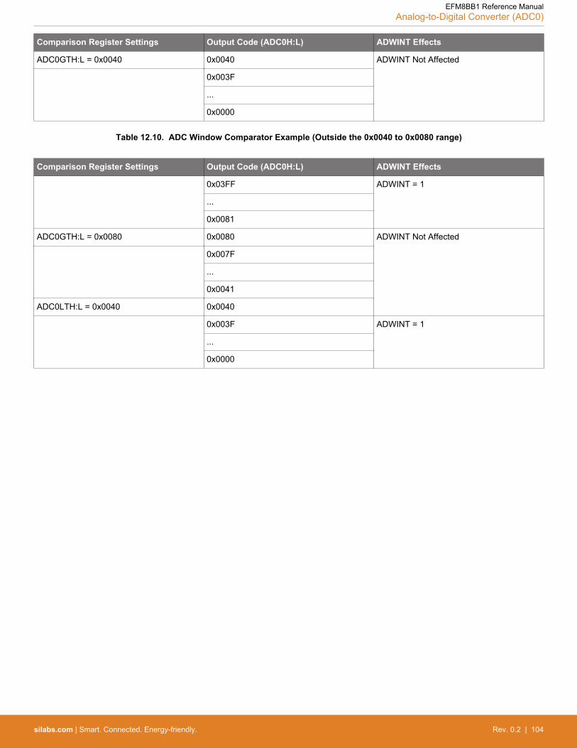
Comparison Register Settings Output Code (ADC0H:L) ADWINT Effects
ADC0GTH:L = 0x0040 0x0040 ADWINT Not Affected
0x003F
...
0x0000
Table 12.10. ADC Window Comparator Example (Outside the 0x0040 to 0x0080 range)
Comparison Register Settings Output Code (ADC0H:L) ADWINT Effects
0x03FF ADWINT = 1
...
0x0081
ADC0GTH:L = 0x0080 0x0080 ADWINT Not Affected
0x007F
...
0x0041
ADC0LTH:L = 0x0040 0x0040
0x003F ADWINT = 1
...
0x0000
EFM8BB1 Reference ManualAnalog-to-Digital Converter (ADC0)
silabs.com | Smart. Connected. Energy-friendly. Rev. 0.2 | 104

12.3.13 Temperature Sensor
An on-chip analog temperature sensor is available to the ADC multiplexer input. To use the ADC to measure the temperature sensor,the ADC mux channel should select the temperature sensor. The temperature sensor transfer function is shown in Figure 12.6 Temper-ature Sensor Transfer Function on page 105. The output voltage (VTEMP) is the positive ADC input when the ADC multiplexer is setcorrectly. The TEMPE bit in register REF0CN enables/ disables the temperature sensor. While disabled, the temperature sensor de-faults to a high impedance state and any ADC measurements performed on the sensor will result in meaningless data. Refer to theelectrical specification tables for the slope and offset parameters of the temperature sensor.
Temperature
= ( Slope x ) + Offset
Offset
Slope
= ( - Offset ) / Slope
Volta
ge
(V at 0 deg Celsius)
(V / deg C)
Temp C
V TEMP
V TEMP
Temp C
Figure 12.6. Temperature Sensor Transfer Function
12.3.13.1 Temperature Sensor Calibration
The uncalibrated temperature sensor output is extremely linear and suitable for relative temperature measurements. For absolute tem-perature measurements, offset and/or gain calibration is recommended. Typically a 1-point (offset) calibration includes the followingsteps:
1. Control/measure the ambient temperature (this temperature must be known).2. Power the device, and delay for a few seconds to allow for self-heating.3. Perform an ADC conversion with the temperature sensor selected as the ADC input.4. Calculate the offset characteristics, and store this value in non-volatile memory for use with subsequent temperature sensor meas-
urements.
EFM8BB1 Reference ManualAnalog-to-Digital Converter (ADC0)
silabs.com | Smart. Connected. Energy-friendly. Rev. 0.2 | 105
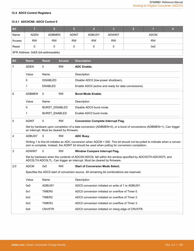
12.4 ADC0 Control Registers
12.4.1 ADC0CN0: ADC0 Control 0
Bit 7 6 5 4 3 2 1 0
Name ADEN ADBMEN ADINT ADBUSY ADWINT ADCM
Access RW RW RW RW RW RW
Reset 0 0 0 0 0 0x0
SFR Address: 0xE8 (bit-addressable)
Bit Name Reset Access Description
7 ADEN 0 RW ADC Enable.
Value Name Description
0 DISABLED Disable ADC0 (low-power shutdown).
1 ENABLED Enable ADC0 (active and ready for data conversions).
6 ADBMEN 0 RW Burst Mode Enable.
Value Name Description
0 BURST_DISABLED Disable ADC0 burst mode.
1 BURST_ENABLED Enable ADC0 burst mode.
5 ADINT 0 RW Conversion Complete Interrupt Flag.
Set by hardware upon completion of a data conversion (ADBMEN=0), or a burst of conversions (ADBMEN=1). Can triggeran interrupt. Must be cleared by firmware.
4 ADBUSY 0 RW ADC Busy.
Writing 1 to this bit initiates an ADC conversion when ADCM = 000. This bit should not be polled to indicate when a conver-sion is complete. Instead, the ADINT bit should be used when polling for conversion completion.
3 ADWINT 0 RW Window Compare Interrupt Flag.
Set by hardware when the contents of ADC0H:ADC0L fall within the window specified by ADC0GTH:ADC0GTL andADC0LTH:ADC0LTL. Can trigger an interrupt. Must be cleared by firmware.
2:0 ADCM 0x0 RW Start of Conversion Mode Select.
Specifies the ADC0 start of conversion source. All remaining bit combinations are reserved.
Value Name Description
0x0 ADBUSY ADC0 conversion initiated on write of 1 to ADBUSY.
0x1 TIMER0 ADC0 conversion initiated on overflow of Timer 0.
0x2 TIMER2 ADC0 conversion initiated on overflow of Timer 2.
0x3 TIMER3 ADC0 conversion initiated on overflow of Timer 3.
0x4 CNVSTR ADC0 conversion initiated on rising edge of CNVSTR.
EFM8BB1 Reference ManualAnalog-to-Digital Converter (ADC0)
silabs.com | Smart. Connected. Energy-friendly. Rev. 0.2 | 106
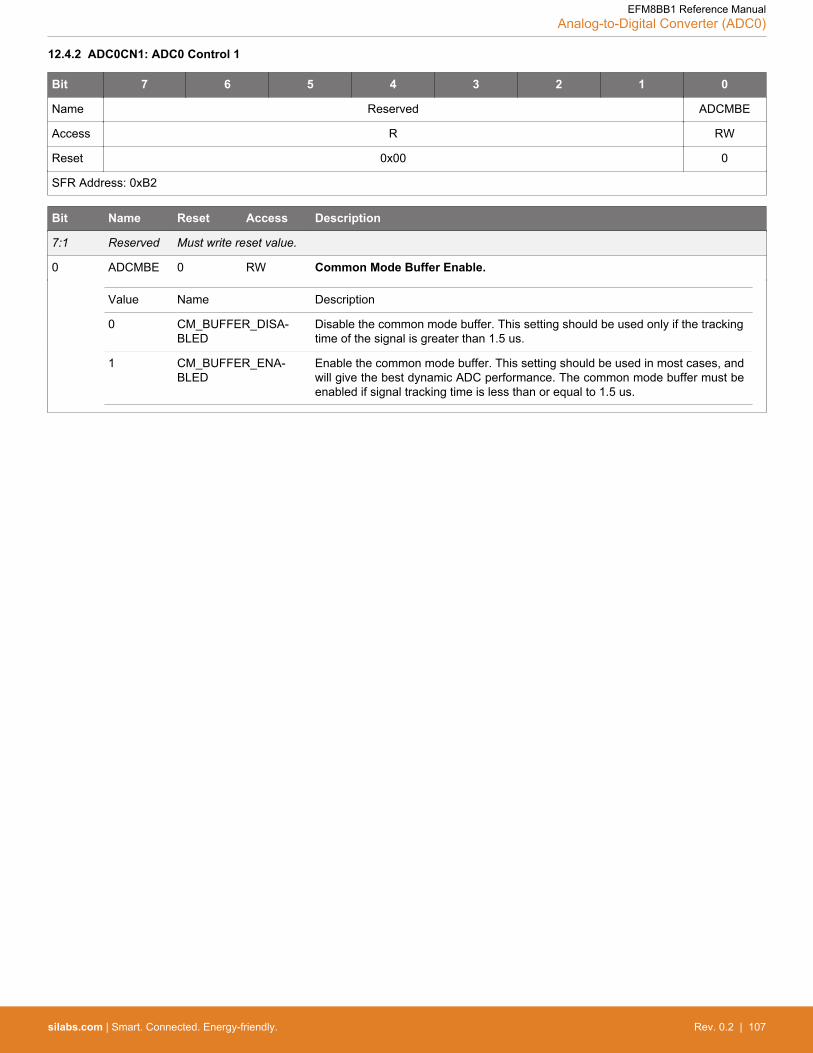
12.4.2 ADC0CN1: ADC0 Control 1
Bit 7 6 5 4 3 2 1 0
Name Reserved ADCMBE
Access R RW
Reset 0x00 0
SFR Address: 0xB2
Bit Name Reset Access Description
7:1 Reserved Must write reset value.
0 ADCMBE 0 RW Common Mode Buffer Enable.
Value Name Description
0 CM_BUFFER_DISA-BLED
Disable the common mode buffer. This setting should be used only if the trackingtime of the signal is greater than 1.5 us.
1 CM_BUFFER_ENA-BLED
Enable the common mode buffer. This setting should be used in most cases, andwill give the best dynamic ADC performance. The common mode buffer must beenabled if signal tracking time is less than or equal to 1.5 us.
EFM8BB1 Reference ManualAnalog-to-Digital Converter (ADC0)
silabs.com | Smart. Connected. Energy-friendly. Rev. 0.2 | 107

12.4.3 ADC0CF: ADC0 Configuration
Bit 7 6 5 4 3 2 1 0
Name ADSC AD8BE ADTM ADGN
Access RW RW RW RW
Reset 0x1F 0 0 0
SFR Address: 0xBC
Bit Name Reset Access Description
7:3 ADSC 0x1F RW SAR Clock Divider.
This field sets the ADC clock divider value. It should be configured to be as close to the maximum SAR clock speed as thedatasheet will allow. The SAR clock frequency is given by the following equation:
Fclksar = (Fadcclk) / (ADSC + 1)
FADCCLK is equal to the selected SYSCLK when ADBMEN is 0 and the high-frequency oscillator when ADBMEN is 1.
2 AD8BE 0 RW 8-Bit Mode Enable.
Value Name Description
0 NORMAL ADC0 operates in 10-bit or 12-bit mode (normal operation).
1 8_BIT ADC0 operates in 8-bit mode.
1 ADTM 0 RW Track Mode.
Selects between Normal or Delayed Tracking Modes.
Value Name Description
0 TRACK_NORMAL Normal Track Mode. When ADC0 is enabled, conversion begins immediately fol-lowing the start-of-conversion signal.
1 TRACK_DELAYED Delayed Track Mode. When ADC0 is enabled, conversion begins 4 SAR clock cy-cles following the start-of-conversion signal. The ADC is allowed to track duringthis time.
0 ADGN 0 RW Gain Control.
Value Name Description
0 GAIN_0P5 The on-chip PGA gain is 0.5.
1 GAIN_1 The on-chip PGA gain is 1.
EFM8BB1 Reference ManualAnalog-to-Digital Converter (ADC0)
silabs.com | Smart. Connected. Energy-friendly. Rev. 0.2 | 108
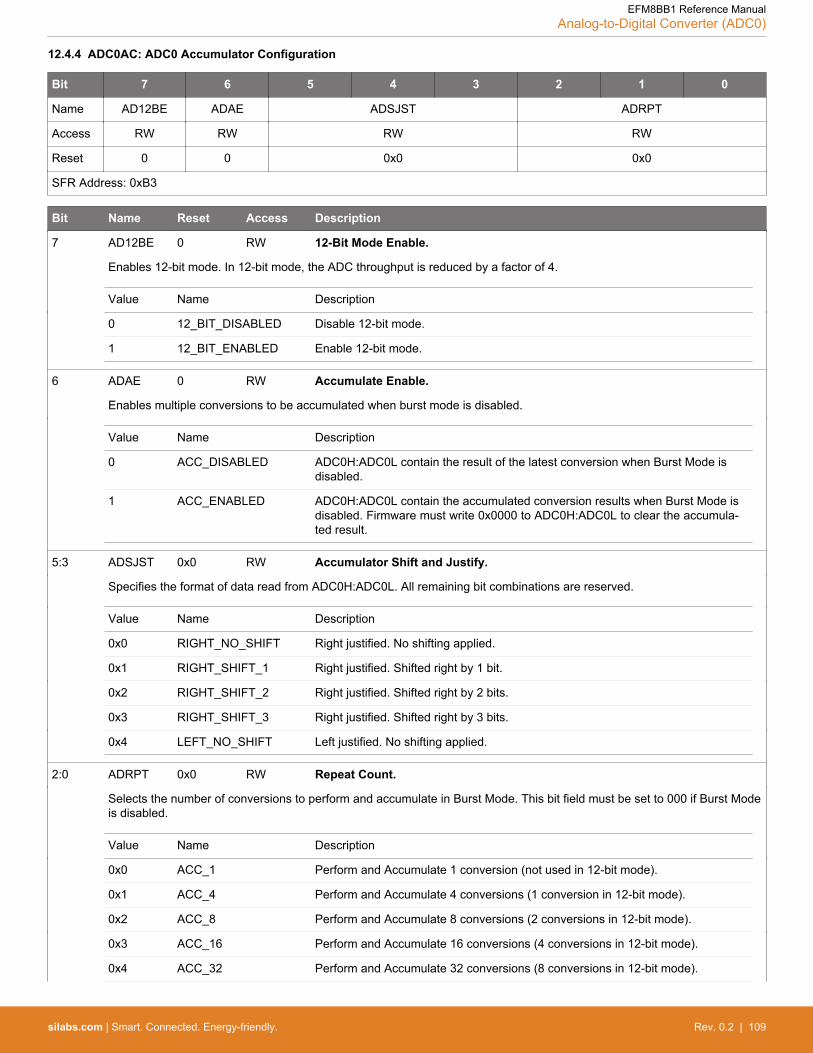
12.4.4 ADC0AC: ADC0 Accumulator Configuration
Bit 7 6 5 4 3 2 1 0
Name AD12BE ADAE ADSJST ADRPT
Access RW RW RW RW
Reset 0 0 0x0 0x0
SFR Address: 0xB3
Bit Name Reset Access Description
7 AD12BE 0 RW 12-Bit Mode Enable.
Enables 12-bit mode. In 12-bit mode, the ADC throughput is reduced by a factor of 4.
Value Name Description
0 12_BIT_DISABLED Disable 12-bit mode.
1 12_BIT_ENABLED Enable 12-bit mode.
6 ADAE 0 RW Accumulate Enable.
Enables multiple conversions to be accumulated when burst mode is disabled.
Value Name Description
0 ACC_DISABLED ADC0H:ADC0L contain the result of the latest conversion when Burst Mode isdisabled.
1 ACC_ENABLED ADC0H:ADC0L contain the accumulated conversion results when Burst Mode isdisabled. Firmware must write 0x0000 to ADC0H:ADC0L to clear the accumula-ted result.
5:3 ADSJST 0x0 RW Accumulator Shift and Justify.
Specifies the format of data read from ADC0H:ADC0L. All remaining bit combinations are reserved.
Value Name Description
0x0 RIGHT_NO_SHIFT Right justified. No shifting applied.
0x1 RIGHT_SHIFT_1 Right justified. Shifted right by 1 bit.
0x2 RIGHT_SHIFT_2 Right justified. Shifted right by 2 bits.
0x3 RIGHT_SHIFT_3 Right justified. Shifted right by 3 bits.
0x4 LEFT_NO_SHIFT Left justified. No shifting applied.
2:0 ADRPT 0x0 RW Repeat Count.
Selects the number of conversions to perform and accumulate in Burst Mode. This bit field must be set to 000 if Burst Modeis disabled.
Value Name Description
0x0 ACC_1 Perform and Accumulate 1 conversion (not used in 12-bit mode).
0x1 ACC_4 Perform and Accumulate 4 conversions (1 conversion in 12-bit mode).
0x2 ACC_8 Perform and Accumulate 8 conversions (2 conversions in 12-bit mode).
0x3 ACC_16 Perform and Accumulate 16 conversions (4 conversions in 12-bit mode).
0x4 ACC_32 Perform and Accumulate 32 conversions (8 conversions in 12-bit mode).
EFM8BB1 Reference ManualAnalog-to-Digital Converter (ADC0)
silabs.com | Smart. Connected. Energy-friendly. Rev. 0.2 | 109

Bit Name Reset Access Description
0x5 ACC_64 Perform and Accumulate 64 conversions (16 conversions in 12-bit mode).
12.4.5 ADC0PWR: ADC0 Power Control
Bit 7 6 5 4 3 2 1 0
Name ADBIAS ADMXLP ADLPM ADPWR
Access RW RW RW RW
Reset 0x0 0 0 0xF
SFR Address: 0xDF
Bit Name Reset Access Description
7:6 ADBIAS 0x0 RW Bias Power Select.
This field can be used to adjust the ADC's power consumption based on the conversion speed. Higher bias currents allowfor faster conversion times.
Value Name Description
0x0 MODE0 Select bias current mode 0. Recommended to use modes 1, 2, or 3.
0x1 MODE1 Select bias current mode 1 (SARCLK <= 16 MHz).
0x2 MODE2 Select bias current mode 2.
0x3 MODE3 Select bias current mode 3 (SARCLK <= 4 MHz).
5 ADMXLP 0 RW Mux and Reference Low Power Mode Enable.
Enables low power mode operation for the multiplexer and voltage reference buffers.
Value Name Description
0 LP_MUX_VREF_DISA-BLED
Low power mode disabled.
1 LP_MUX_VREF_ENA-BLED
Low power mode enabled (SAR clock < 4 MHz).
4 ADLPM 0 RW Low Power Mode Enable.
This bit can be used to reduce power to the ADC's internal common mode buffer. It can be set to 1 to reduce power whentracking times in the application are longer (slower sample rates).
Value Name Description
0 LP_BUFFER_DISA-BLED
Disable low power mode.
1 LP_BUFFER_ENA-BLED
Enable low power mode (requires extended tracking time).
3:0 ADPWR 0xF RW Burst Mode Power Up Time.
This field sets the time delay allowed for the ADC to power up from a low power state. When ADTM is set, an additional 4SARCLKs are added to this time.
Tpwrtime = (8 * ADPWR) / (Fhfosc)
EFM8BB1 Reference ManualAnalog-to-Digital Converter (ADC0)
silabs.com | Smart. Connected. Energy-friendly. Rev. 0.2 | 110
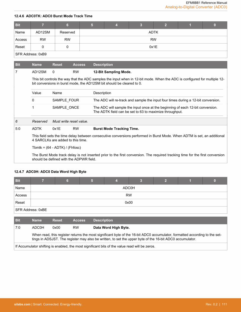
12.4.6 ADC0TK: ADC0 Burst Mode Track Time
Bit 7 6 5 4 3 2 1 0
Name AD12SM Reserved ADTK
Access RW RW RW
Reset 0 0 0x1E
SFR Address: 0xB9
Bit Name Reset Access Description
7 AD12SM 0 RW 12-Bit Sampling Mode.
This bit controls the way that the ADC samples the input when in 12-bit mode. When the ADC is configured for multiple 12-bit conversions in burst mode, the AD12SM bit should be cleared to 0.
Value Name Description
0 SAMPLE_FOUR The ADC will re-track and sample the input four times during a 12-bit conversion.
1 SAMPLE_ONCE The ADC will sample the input once at the beginning of each 12-bit conversion.The ADTK field can be set to 63 to maximize throughput.
6 Reserved Must write reset value.
5:0 ADTK 0x1E RW Burst Mode Tracking Time.
This field sets the time delay between consecutive conversions performed in Burst Mode. When ADTM is set, an additional4 SARCLKs are added to this time.
Tbmtk = (64 - ADTK) / (Fhfosc)
The Burst Mode track delay is not inserted prior to the first conversion. The required tracking time for the first conversionshould be defined with the ADPWR field.
12.4.7 ADC0H: ADC0 Data Word High Byte
Bit 7 6 5 4 3 2 1 0
Name ADC0H
Access RW
Reset 0x00
SFR Address: 0xBE
Bit Name Reset Access Description
7:0 ADC0H 0x00 RW Data Word High Byte.
When read, this register returns the most significant byte of the 16-bit ADC0 accumulator, formatted according to the set-tings in ADSJST. The register may also be written, to set the upper byte of the 16-bit ADC0 accumulator.
If Accumulator shifting is enabled, the most significant bits of the value read will be zeros.
EFM8BB1 Reference ManualAnalog-to-Digital Converter (ADC0)
silabs.com | Smart. Connected. Energy-friendly. Rev. 0.2 | 111
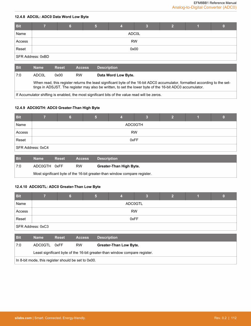
12.4.8 ADC0L: ADC0 Data Word Low Byte
Bit 7 6 5 4 3 2 1 0
Name ADC0L
Access RW
Reset 0x00
SFR Address: 0xBD
Bit Name Reset Access Description
7:0 ADC0L 0x00 RW Data Word Low Byte.
When read, this register returns the least significant byte of the 16-bit ADC0 accumulator, formatted according to the set-tings in ADSJST. The register may also be written, to set the lower byte of the 16-bit ADC0 accumulator.
If Accumulator shifting is enabled, the most significant bits of the value read will be zeros.
12.4.9 ADC0GTH: ADC0 Greater-Than High Byte
Bit 7 6 5 4 3 2 1 0
Name ADC0GTH
Access RW
Reset 0xFF
SFR Address: 0xC4
Bit Name Reset Access Description
7:0 ADC0GTH 0xFF RW Greater-Than High Byte.
Most significant byte of the 16-bit greater-than window compare register.
12.4.10 ADC0GTL: ADC0 Greater-Than Low Byte
Bit 7 6 5 4 3 2 1 0
Name ADC0GTL
Access RW
Reset 0xFF
SFR Address: 0xC3
Bit Name Reset Access Description
7:0 ADC0GTL 0xFF RW Greater-Than Low Byte.
Least significant byte of the 16-bit greater-than window compare register.
In 8-bit mode, this register should be set to 0x00.
EFM8BB1 Reference ManualAnalog-to-Digital Converter (ADC0)
silabs.com | Smart. Connected. Energy-friendly. Rev. 0.2 | 112
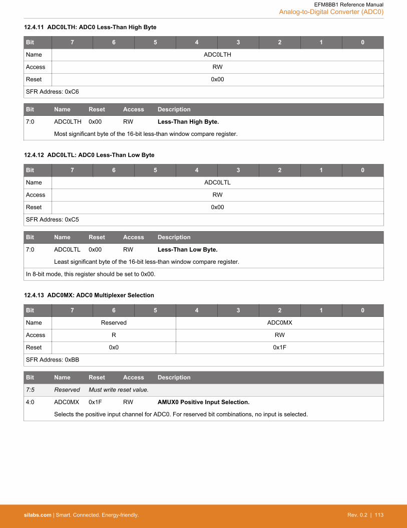
12.4.11 ADC0LTH: ADC0 Less-Than High Byte
Bit 7 6 5 4 3 2 1 0
Name ADC0LTH
Access RW
Reset 0x00
SFR Address: 0xC6
Bit Name Reset Access Description
7:0 ADC0LTH 0x00 RW Less-Than High Byte.
Most significant byte of the 16-bit less-than window compare register.
12.4.12 ADC0LTL: ADC0 Less-Than Low Byte
Bit 7 6 5 4 3 2 1 0
Name ADC0LTL
Access RW
Reset 0x00
SFR Address: 0xC5
Bit Name Reset Access Description
7:0 ADC0LTL 0x00 RW Less-Than Low Byte.
Least significant byte of the 16-bit less-than window compare register.
In 8-bit mode, this register should be set to 0x00.
12.4.13 ADC0MX: ADC0 Multiplexer Selection
Bit 7 6 5 4 3 2 1 0
Name Reserved ADC0MX
Access R RW
Reset 0x0 0x1F
SFR Address: 0xBB
Bit Name Reset Access Description
7:5 Reserved Must write reset value.
4:0 ADC0MX 0x1F RW AMUX0 Positive Input Selection.
Selects the positive input channel for ADC0. For reserved bit combinations, no input is selected.
EFM8BB1 Reference ManualAnalog-to-Digital Converter (ADC0)
silabs.com | Smart. Connected. Energy-friendly. Rev. 0.2 | 113

12.4.14 REF0CN: Voltage Reference Control
Bit 7 6 5 4 3 2 1 0
Name IREFLVL Reserved GNDSL REFSL TEMPE Reserved
Access RW R RW RW RW R
Reset 0 0 0 0x3 0 0x0
SFR Address: 0xD1
Bit Name Reset Access Description
7 IREFLVL 0 RW Internal Voltage Reference Level.
Sets the voltage level for the internal reference source.
Value Name Description
0 1P65 The internal reference operates at 1.65 V nominal.
1 2P4 The internal reference operates at 2.4 V nominal.
6 Reserved Must write reset value.
5 GNDSL 0 RW Analog Ground Reference.
Selects the ADC0 ground reference.
Value Name Description
0 GND_PIN The ADC0 ground reference is the GND pin.
1 AGND_PIN The ADC0 ground reference is the P0.1/AGND pin.
4:3 REFSL 0x3 RW Voltage Reference Select.
Selects the ADC0 voltage reference.
Value Name Description
0x0 VREF_PIN The ADC0 voltage reference is the P0.0/VREF pin.
0x1 VDD_PIN The ADC0 voltage reference is the VDD pin.
0x2 INTERNAL_LDO The ADC0 voltage reference is the internal 1.8 V digital supply voltage.
0x3 INTERNAL_VREF The ADC0 voltage reference is the internal voltage reference.
2 TEMPE 0 RW Temperature Sensor Enable.
Enables/Disables the internal temperature sensor.
Value Name Description
0 TEMP_DISABLED Disable the Temperature Sensor.
1 TEMP_ENABLED Enable the Temperature Sensor.
1:0 Reserved Must write reset value.
EFM8BB1 Reference ManualAnalog-to-Digital Converter (ADC0)
silabs.com | Smart. Connected. Energy-friendly. Rev. 0.2 | 114

13. Comparators (CMP0 and CMP1)
13.1 Introduction
Analog comparators are used to compare the voltage of two analog inputs, with a digital output indicating which input voltage is higher.External input connections to device I/O pins and internal connections are available through separate multiplexers on the positive andnegative inputs. Hysteresis, response time, and current consumption may be programmed to suit the specific needs of the application.
CMPn
CMPn+
CMPn-
Programmable Hysteresis
Programmable Response Time
D
Q
Q
CPn(synchronous)
CPnA(asynchronous)
SYSCLK
GND
Port Pins
Negative Input Selection
Port Pins
Positive Input Selection
Internal LDO
Figure 13.1. Comparator Block Diagram
13.2 Features
The comparator module includes the following features:• Up to 8 external positive inputs.• Up to 8 external negative inputs.• Additional input options:
• Internal connection to LDO output.• Direct connection to GND.
• Synchronous and asynchronous outputs can be routed to pins via crossbar.• Programmable hysteresis between 0 and ±20 mV• Programmable response time.• Interrupts generated on rising, falling, or both edges.
13.3 Functional Description
13.3.1 Response Time and Supply Current
Response time is the amount of time delay between a change at the comparator inputs and the comparator's reaction at the output.The comparator response time may be configured in software via the CPMD field in the CMPnMD register. Selecting a longer responsetime reduces the comparator supply current, while shorter response times require more supply current.
EFM8BB1 Reference ManualComparators (CMP0 and CMP1)
silabs.com | Smart. Connected. Energy-friendly. Rev. 0.2 | 115

13.3.2 Hysteresis
The comparator hysteresis is software-programmable via its Comparator Control register CMPnCN. The user can program both theamount of hysteresis voltage (referred to the input voltage) and the positive and negative-going symmetry of this hysteresis around thethreshold voltage.
The comparator hysteresis is programmable using the CPHYN and CPHYP fields in the Comparator Control Register CMPnCN. Theamount of negative hysteresis voltage is determined by the settings of the CPHYN bits. Settings of 20, 10, or 5 mV (nominal) of nega-tive hysteresis can be programmed, or negative hysteresis can be disabled. In a similar way, the amount of positive hysteresis is deter-mined by the setting the CPHYP bits.
CPn-
Positive programmable hysteresis (CPHYP)
CPn+Negative programmable
hysteresis (CPHYN)
CP0 (out)
Figure 13.2. Comparator Hysteresis Plot
13.3.3 Input Selection
Comparator inputs may be routed to port I/O pins or internal signals. When connected externally, the comparator inputs can be drivenfrom –0.25 V to (VDD) +0.25 V without damage or upset. The CMPnMX register selects the inputs for the associated comparator. TheCMXP field selects the comparator’s positive input (CPnP.x) and the CMXN field selects the comparator’s negative input (CPnN.x).Note: Any port pins selected as comparator inputs should be configured as analog inputs in their associated port configuration register,and configured to be skipped by the crossbar.
EFM8BB1 Reference ManualComparators (CMP0 and CMP1)
silabs.com | Smart. Connected. Energy-friendly. Rev. 0.2 | 116

13.3.3.1 Multiplexer Channel Selection
Table 13.1. CMP0 Positive Input Multiplexer Channels
CMXP Setting inRegisterCMP0MX
Signal Name Enumeration Name QSOP24 PinName
QFN20 PinName
SOIC16 PinName
0000 CMP0P.0 CMP0P0 P0.0 P0.0 P0.0
0001 CMP0P.1 CMP0P1 P0.1 P0.1 P0.1
0010 CMP0P.2 CMP0P2 P0.2 P0.2 P0.2
0011 CMP0P.3 CMP0P3 P0.3 P0.3 P0.3
0100 CMP0P.4 CMP0P4 P0.4 P0.4 P0.4
0101 CMP0P.5 CMP0P5 P0.5 P0.5 P0.5
0110 CMP0P.6 CMP0P6 P0.6 P0.6 No connection /Reserved
0111 CMP0P.7 CMP0P7 P0.7 P0.7 No connection /Reserved
1000 CMP0P.8 LDO_OUT Internal 1.8V LDO output
1001-1111 CMP0P.9 - CMP0P.15 NONE No connection / Reserved
Table 13.2. CMP0 Negative Input Multiplexer Channels
CMXN Setting inRegisterCMP0MX
Signal Name Enumeration Name QSOP24 PinName
QFN20 PinName
SOIC16 PinName
0000 CMP0N.0 CMP0N0 P0.0 P0.0 P0.0
0001 CMP0N.1 CMP0N1 P0.1 P0.1 P0.1
0010 CMP0N.2 CMP0N2 P0.2 P0.2 P0.2
0011 CMP0N.3 CMP0N3 P0.3 P0.3 P0.3
0100 CMP0N.4 CMP0N4 P0.4 P0.4 P0.4
0101 CMP0N.5 CMP0N5 P0.5 P0.5 P0.5
0110 CMP0N.6 CMP0N6 P0.6 P0.6 No connection /Reserved
0111 CMP0N.7 CMP0N7 P0.7 P0.7 No connection /Reserved
1000 CMP0P.8 GND GND Supply Pin
1001-1111 CMP0P.9 - CMP0P.15 NONE No connection / Reserved
Table 13.3. CMP1 Positive Input Multiplexer Channels
CMXP Setting inRegisterCMP1MX
Signal Name Enumeration Name QSOP24 PinName
QFN20 PinName
SOIC16 PinName
0000 CMP1P.0 CMP1P0 P1.0 P1.0 P0.6
0001 CMP1P.1 CMP1P1 P1.1 P1.1 P0.7
EFM8BB1 Reference ManualComparators (CMP0 and CMP1)
silabs.com | Smart. Connected. Energy-friendly. Rev. 0.2 | 117

CMXP Setting inRegisterCMP1MX
Signal Name Enumeration Name QSOP24 PinName
QFN20 PinName
SOIC16 PinName
0010 CMP1P.2 CMP1P2 P1.2 P1.2 P1.0
0011 CMP1P.3 CMP1P3 P1.3 P1.3 P1.1
0100 CMP1P.4 CMP1P4 P1.4 P1.4 P1.2
0101 CMP1P.5 CMP1P5 P1.5 P1.5 P1.3
0110 CMP1P.6 CMP1P6 P1.6 P1.6 No connection /Reserved
0111 CMP1P.7 CMP1P7 P1.7 No connection /Reserved
No connection /Reserved
1000 CMP1P.8 LDO_OUT Internal 1.8V LDO output
1001-1111 CMP1P.9 - CMP1P.15 NONE No connection / Reserved
Table 13.4. CMP1 Negative Input Multiplexer Channels
CMXN Setting inRegisterCMP1MX
Signal Name Enumeration Name QSOP24 PinName
QFN20 PinName
SOIC16 PinName
0000 CMP1N.0 CMP1N0 P1.0 P1.0 P0.6
0001 CMP1N.1 CMP1N1 P1.1 P1.1 P0.7
0010 CMP1N.2 CMP1N2 P1.2 P1.2 P1.0
0011 CMP1N.3 CMP1N3 P1.3 P1.3 P1.1
0100 CMP1N.4 CMP1N4 P1.4 P1.4 P1.2
0101 CMP1N.5 CMP1N5 P1.5 P1.5 P1.3
0110 CMP1N.6 CMP1N6 P1.6 P1.6 No connection /Reserved
0111 CMP1N.7 CMP1N7 P1.7 No connection /Reserved
No connection /Reserved
1000 CMP1P.8 GND GND Supply Pin
1001-1111 CMP1P.9 - CMP1P.15 NONE No connection / Reserved
13.3.4 Output Routing
The comparator’s synchronous and asynchronous outputs can optionally be routed to port I/O pins through the port I/O crossbar. Theoutput of either comparator may be configured to generate a system interrupt on rising, falling, or both edges. CMP0 may also be usedas a reset source or as a trigger to kill a PCA output channel.
The output state of the comparator can be obtained at any time by reading the CPOUT bit. The comparator is enabled by setting theCPEN bit to logic 1, and is disabled by clearing this bit to logic 0. When disabled, the comparator output (if assigned to a port I/O pin viathe crossbar) defaults to the logic low state, and the power supply to the comparator is turned off.
Comparator interrupts can be generated on both rising-edge and falling-edge output transitions. The CPFIF flag is set to logic 1 upon acomparator falling-edge occurrence, and the CPRIF flag is set to logic 1 upon the comparator rising-edge occurrence. Once set, thesebits remain set until cleared by software. The comparator rising-edge interrupt mask is enabled by setting CPRIE to a logic 1. The com-parator falling-edge interrupt mask is enabled by setting CPFIE to a logic 1.
False rising edges and falling edges may be detected when the comparator is first powered on or if changes are made to the hysteresisor response time control bits. Therefore, it is recommended that the rising-edge and falling-edge flags be explicitly cleared to logic 0 ashort time after the comparator is enabled or its mode bits have been changed, before enabling comparator interrupts.
EFM8BB1 Reference ManualComparators (CMP0 and CMP1)
silabs.com | Smart. Connected. Energy-friendly. Rev. 0.2 | 118

13.4 CMP0 Control Registers
13.4.1 CMP0CN0: Comparator 0 Control 0
Bit 7 6 5 4 3 2 1 0
Name CPEN CPOUT CPRIF CPFIF CPHYP CPHYN
Access RW R RW RW RW RW
Reset 0 0 0 0 0x0 0x0
SFR Address: 0x9B
Bit Name Reset Access Description
7 CPEN 0 RW Comparator Enable.
Value Name Description
0 DISABLED Comparator disabled.
1 ENABLED Comparator enabled.
6 CPOUT 0 R Comparator Output State Flag.
Value Name Description
0 POS_LESS_THAN_NEG
Voltage on CP0P < CP0N.
1 POS_GREAT-ER_THAN_NEG
Voltage on CP0P > CP0N.
5 CPRIF 0 RW Comparator Rising-Edge Flag.
Must be cleared by firmware.
Value Name Description
0 NOT_SET No comparator rising edge has occurred since this flag was last cleared.
1 RISING_EDGE Comparator rising edge has occurred.
4 CPFIF 0 RW Comparator Falling-Edge Flag.
Must be cleared by firmware.
Value Name Description
0 NOT_SET No comparator falling edge has occurred since this flag was last cleared.
1 FALLING_EDGE Comparator falling edge has occurred.
3:2 CPHYP 0x0 RW Comparator Positive Hysteresis Control.
Value Name Description
0x0 DISABLED Positive Hysteresis disabled.
0x1 ENABLED_MODE1 Positive Hysteresis = Hysteresis 1.
0x2 ENABLED_MODE2 Positive Hysteresis = Hysteresis 2.
0x3 ENABLED_MODE3 Positive Hysteresis = Hysteresis 3 (Maximum).
1:0 CPHYN 0x0 RW Comparator Negative Hysteresis Control.
EFM8BB1 Reference ManualComparators (CMP0 and CMP1)
silabs.com | Smart. Connected. Energy-friendly. Rev. 0.2 | 119

Bit Name Reset Access Description
Value Name Description
0x0 DISABLED Negative Hysteresis disabled.
0x1 ENABLED_MODE1 Negative Hysteresis = Hysteresis 1.
0x2 ENABLED_MODE2 Negative Hysteresis = Hysteresis 2.
0x3 ENABLED_MODE3 Negative Hysteresis = Hysteresis 3 (Maximum).
EFM8BB1 Reference ManualComparators (CMP0 and CMP1)
silabs.com | Smart. Connected. Energy-friendly. Rev. 0.2 | 120

13.4.2 CMP0MD: Comparator 0 Mode
Bit 7 6 5 4 3 2 1 0
Name CPLOUT Reserved CPRIE CPFIE Reserved CPMD
Access RW R RW RW R RW
Reset 0 0 0 0 0x0 0x2
SFR Address: 0x9D
Bit Name Reset Access Description
7 CPLOUT 0 RW Comparator Latched Output Flag.
This bit represents the comparator output value at the most recent PCA counter overflow.
Value Name Description
0 LOW Comparator output was logic low at last PCA overflow.
1 HIGH Comparator output was logic high at last PCA overflow.
6 Reserved Must write reset value.
5 CPRIE 0 RW Comparator Rising-Edge Interrupt Enable.
Value Name Description
0 RISE_INT_DISABLED Comparator rising-edge interrupt disabled.
1 RISE_INT_ENABLED Comparator rising-edge interrupt enabled.
4 CPFIE 0 RW Comparator Falling-Edge Interrupt Enable.
Value Name Description
0 FALL_INT_DISABLED Comparator falling-edge interrupt disabled.
1 FALL_INT_ENABLED Comparator falling-edge interrupt enabled.
3:2 Reserved Must write reset value.
1:0 CPMD 0x2 RW Comparator Mode Select.
These bits affect the response time and power consumption of the comparator.
Value Name Description
0x0 MODE0 Mode 0 (Fastest Response Time, Highest Power Consumption)
0x1 MODE1 Mode 1
0x2 MODE2 Mode 2
0x3 MODE3 Mode 3 (Slowest Response Time, Lowest Power Consumption)
EFM8BB1 Reference ManualComparators (CMP0 and CMP1)
silabs.com | Smart. Connected. Energy-friendly. Rev. 0.2 | 121
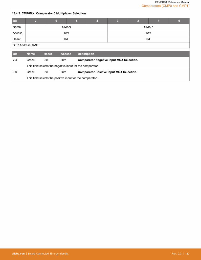
13.4.3 CMP0MX: Comparator 0 Multiplexer Selection
Bit 7 6 5 4 3 2 1 0
Name CMXN CMXP
Access RW RW
Reset 0xF 0xF
SFR Address: 0x9F
Bit Name Reset Access Description
7:4 CMXN 0xF RW Comparator Negative Input MUX Selection.
This field selects the negative input for the comparator.
3:0 CMXP 0xF RW Comparator Positive Input MUX Selection.
This field selects the positive input for the comparator.
EFM8BB1 Reference ManualComparators (CMP0 and CMP1)
silabs.com | Smart. Connected. Energy-friendly. Rev. 0.2 | 122

13.5 CMP1 Control Registers
13.5.1 CMP1CN0: Comparator 1 Control 0
Bit 7 6 5 4 3 2 1 0
Name CPEN CPOUT CPRIF CPFIF CPHYP CPHYN
Access RW R RW RW RW RW
Reset 0 0 0 0 0x0 0x0
SFR Address: 0xBF
Bit Name Reset Access Description
7 CPEN 0 RW Comparator Enable.
Value Name Description
0 DISABLED Comparator disabled.
1 ENABLED Comparator enabled.
6 CPOUT 0 R Comparator Output State Flag.
Value Name Description
0 POS_LESS_THAN_NEG
Voltage on CP1P < CP1N.
1 POS_GREAT-ER_THAN_NEG
Voltage on CP1P > CP1N.
5 CPRIF 0 RW Comparator Rising-Edge Flag.
Must be cleared by firmware.
Value Name Description
0 NOT_SET No comparator rising edge has occurred since this flag was last cleared.
1 RISING_EDGE Comparator rising edge has occurred.
4 CPFIF 0 RW Comparator Falling-Edge Flag.
Must be cleared by firmware.
Value Name Description
0 NOT_SET No comparator falling edge has occurred since this flag was last cleared.
1 FALLING_EDGE Comparator falling edge has occurred.
3:2 CPHYP 0x0 RW Comparator Positive Hysteresis Control.
Value Name Description
0x0 DISABLED Positive Hysteresis disabled.
0x1 ENABLED_MODE1 Positive Hysteresis = Hysteresis 1.
0x2 ENABLED_MODE2 Positive Hysteresis = Hysteresis 2.
0x3 ENABLED_MODE3 Positive Hysteresis = Hysteresis 3 (Maximum).
1:0 CPHYN 0x0 RW Comparator Negative Hysteresis Control.
EFM8BB1 Reference ManualComparators (CMP0 and CMP1)
silabs.com | Smart. Connected. Energy-friendly. Rev. 0.2 | 123

Bit Name Reset Access Description
Value Name Description
0x0 DISABLED Negative Hysteresis disabled.
0x1 ENABLED_MODE1 Negative Hysteresis = Hysteresis 1.
0x2 ENABLED_MODE2 Negative Hysteresis = Hysteresis 2.
0x3 ENABLED_MODE3 Negative Hysteresis = Hysteresis 3 (Maximum).
EFM8BB1 Reference ManualComparators (CMP0 and CMP1)
silabs.com | Smart. Connected. Energy-friendly. Rev. 0.2 | 124
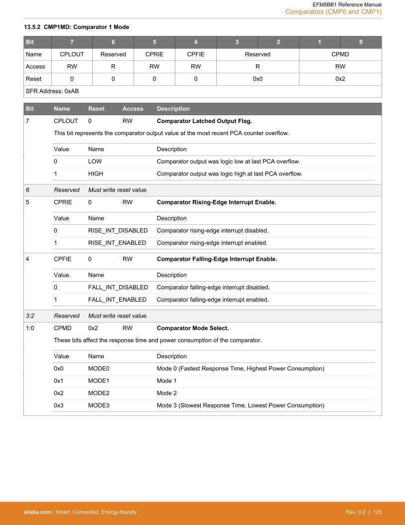
13.5.2 CMP1MD: Comparator 1 Mode
Bit 7 6 5 4 3 2 1 0
Name CPLOUT Reserved CPRIE CPFIE Reserved CPMD
Access RW R RW RW R RW
Reset 0 0 0 0 0x0 0x2
SFR Address: 0xAB
Bit Name Reset Access Description
7 CPLOUT 0 RW Comparator Latched Output Flag.
This bit represents the comparator output value at the most recent PCA counter overflow.
Value Name Description
0 LOW Comparator output was logic low at last PCA overflow.
1 HIGH Comparator output was logic high at last PCA overflow.
6 Reserved Must write reset value.
5 CPRIE 0 RW Comparator Rising-Edge Interrupt Enable.
Value Name Description
0 RISE_INT_DISABLED Comparator rising-edge interrupt disabled.
1 RISE_INT_ENABLED Comparator rising-edge interrupt enabled.
4 CPFIE 0 RW Comparator Falling-Edge Interrupt Enable.
Value Name Description
0 FALL_INT_DISABLED Comparator falling-edge interrupt disabled.
1 FALL_INT_ENABLED Comparator falling-edge interrupt enabled.
3:2 Reserved Must write reset value.
1:0 CPMD 0x2 RW Comparator Mode Select.
These bits affect the response time and power consumption of the comparator.
Value Name Description
0x0 MODE0 Mode 0 (Fastest Response Time, Highest Power Consumption)
0x1 MODE1 Mode 1
0x2 MODE2 Mode 2
0x3 MODE3 Mode 3 (Slowest Response Time, Lowest Power Consumption)
EFM8BB1 Reference ManualComparators (CMP0 and CMP1)
silabs.com | Smart. Connected. Energy-friendly. Rev. 0.2 | 125
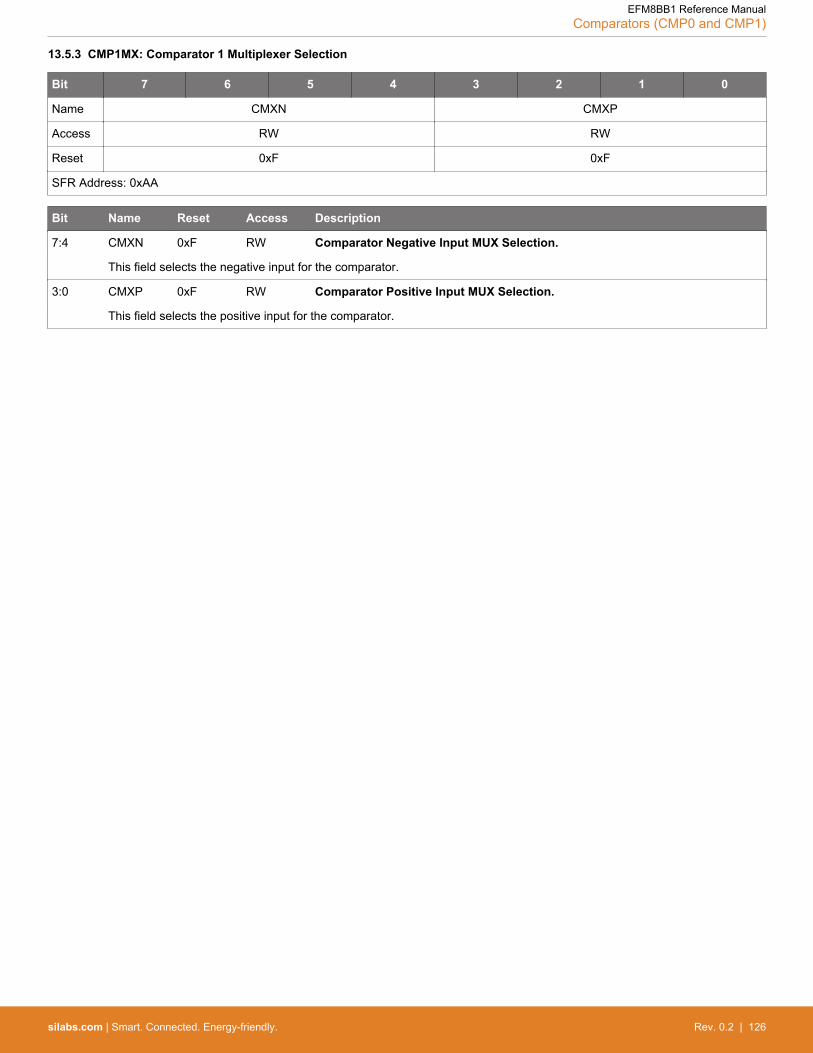
13.5.3 CMP1MX: Comparator 1 Multiplexer Selection
Bit 7 6 5 4 3 2 1 0
Name CMXN CMXP
Access RW RW
Reset 0xF 0xF
SFR Address: 0xAA
Bit Name Reset Access Description
7:4 CMXN 0xF RW Comparator Negative Input MUX Selection.
This field selects the negative input for the comparator.
3:0 CMXP 0xF RW Comparator Positive Input MUX Selection.
This field selects the positive input for the comparator.
EFM8BB1 Reference ManualComparators (CMP0 and CMP1)
silabs.com | Smart. Connected. Energy-friendly. Rev. 0.2 | 126

14. Cyclic Redundancy Check (CRC0)
14.1 Introduction
The cyclic redundancy check (CRC) module performs a CRC using a 16-bit polynomial. CRC0 accepts a stream of 8-bit data and poststhe 16-bit result to an internal register. In addition to using the CRC block for data manipulation, hardware can automatically CRC theflash contents of the device.
CRC
CRC0DAT
CRC0IN
byte-level bit reversal
Hardware CRC Calculation UnitSeed
(0x0000 or 0xFFFF)
Automatic flash read
control
8 8
8
8
8Flash Memory
CRC0FLIP 8
Figure 14.1. CRC Functional Block Diagram
14.2 Features
The CRC module is designed to provide hardware calculations for flash memory verification and communications protocols. The CRCmodule supports the standard CCITT-16 16-bit polynomial (0x1021), and includes the following features:• Support for CCITT-16 polynomial• Byte-level bit reversal• Automatic CRC of flash contents on one or more 256-byte blocks• Initial seed selection of 0x0000 or 0xFFFF
EFM8BB1 Reference ManualCyclic Redundancy Check (CRC0)
silabs.com | Smart. Connected. Energy-friendly. Rev. 0.2 | 127
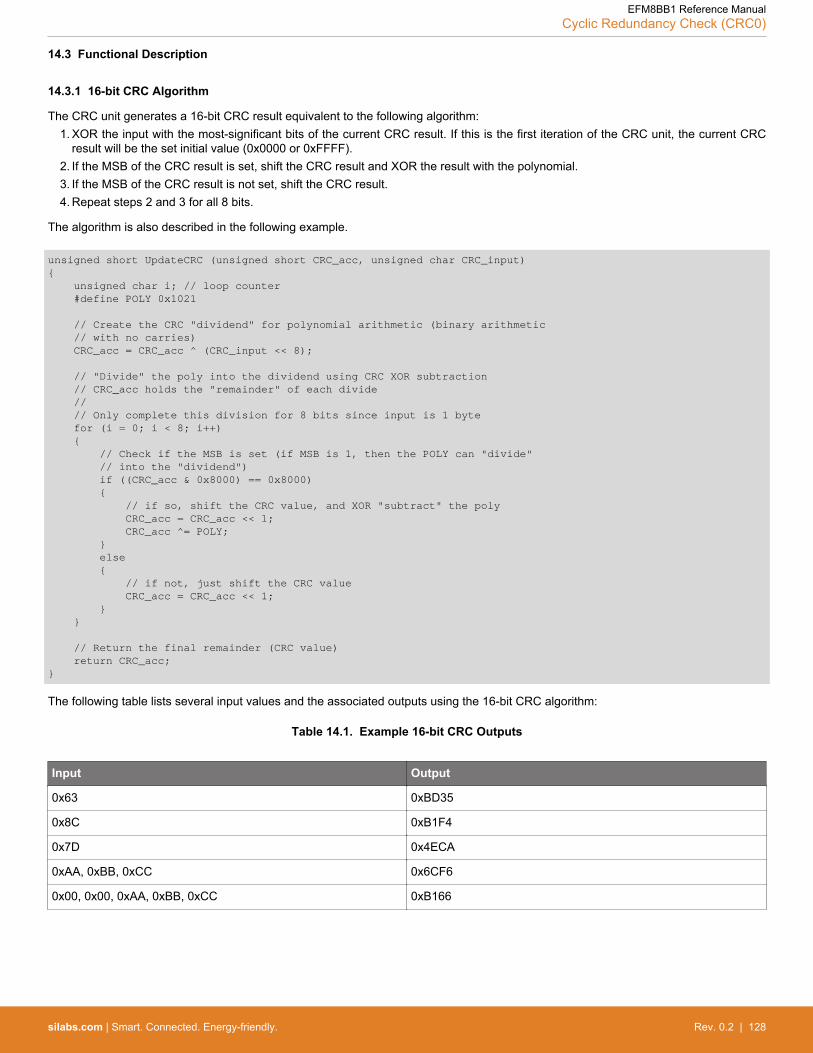
14.3 Functional Description
14.3.1 16-bit CRC Algorithm
The CRC unit generates a 16-bit CRC result equivalent to the following algorithm:1. XOR the input with the most-significant bits of the current CRC result. If this is the first iteration of the CRC unit, the current CRC
result will be the set initial value (0x0000 or 0xFFFF).2. If the MSB of the CRC result is set, shift the CRC result and XOR the result with the polynomial.3. If the MSB of the CRC result is not set, shift the CRC result.4. Repeat steps 2 and 3 for all 8 bits.
The algorithm is also described in the following example.
unsigned short UpdateCRC (unsigned short CRC_acc, unsigned char CRC_input){ unsigned char i; // loop counter #define POLY 0x1021
// Create the CRC "dividend" for polynomial arithmetic (binary arithmetic // with no carries) CRC_acc = CRC_acc ^ (CRC_input << 8);
// "Divide" the poly into the dividend using CRC XOR subtraction // CRC_acc holds the "remainder" of each divide // // Only complete this division for 8 bits since input is 1 byte for (i = 0; i < 8; i++) { // Check if the MSB is set (if MSB is 1, then the POLY can "divide" // into the "dividend") if ((CRC_acc & 0x8000) == 0x8000) { // if so, shift the CRC value, and XOR "subtract" the poly CRC_acc = CRC_acc << 1; CRC_acc ^= POLY; } else { // if not, just shift the CRC value CRC_acc = CRC_acc << 1; } }
// Return the final remainder (CRC value) return CRC_acc;}
The following table lists several input values and the associated outputs using the 16-bit CRC algorithm:
Table 14.1. Example 16-bit CRC Outputs
Input Output
0x63 0xBD35
0x8C 0xB1F4
0x7D 0x4ECA
0xAA, 0xBB, 0xCC 0x6CF6
0x00, 0x00, 0xAA, 0xBB, 0xCC 0xB166
EFM8BB1 Reference ManualCyclic Redundancy Check (CRC0)
silabs.com | Smart. Connected. Energy-friendly. Rev. 0.2 | 128

14.3.2 Using the CRC on a Data Stream
The CRC module may be used to perform CRC calculations on any data set available to the firmware. To perform a CRC on an arbitra-ry data sream:
1. Select the initial result value using CRCVAL.2. Set the result to its initial value (write 1 to CRCINIT).3. Write the data to CRC0IN one byte at a time. The CRC result registers are automatically updated after each byte is written.4. Write the CRCPNT bit to 0 to target the low byte of the result.5. Read CRC0DAT multiple times to access each byte of the CRC result. CRCPNT will automatically point to the next value after
each read.
14.3.3 Using the CRC to Check Code Memory
The CRC module may be configured to automatically perform a CRC on one or more blocks of code memory. To perform a CRC oncode contents:
1. Select the initial result value using CRCVAL.2. Set the result to its initial value (write 1 to CRCINIT).3. Write the high byte of the starting address to the CRCST bit field.4. Set the AUTOEN bit to 1.5. Write the number of byte blocks to perform in the CRC calculation to CRCCNT.6. Write any value to CRC0CN0 (or OR its contents with 0x00) to initiate the CRC calculation. The CPU will not execute code any
additional code until the CRC operation completes.Note: Upon initiation of an automatic CRC calculation, the three cycles following a write to CRC0CN0 that initiate a CRC operationmust only contain instructions which execute in the same number of cycles as the number of bytes in the instruction. An example ofsuch an instruction is a 3-byte MOV that targets the CRC0FLIP register. When programming in C, the dummy value written toCRC0FLIP should be a non-zero value to prevent the compiler from generating a 2-byte MOV instruction.
7. Clear the AUTOEN.8. Write the CRCPNT bit to 0 to target the low byte of the result.9. Read CRC0DAT multiple times to access each byte of the CRC result. CRCPNT will automatically point to the next value after
each read.
14.3.4 Bit Reversal
CRC0 includes hardware to reverse the bit order of each bit in a byte. Writing a byte to CRC0FLIP initiates the bit reversal operation,and the result may be read back from CRC0FLIP on the next instruction. For example, if 0xC0 is written to CRC0FLIP, the data readback is 0x03. Bit reversal can be used to change the order of information passing through the CRC engine and is also used in algo-rithms such as FFT.
EFM8BB1 Reference ManualCyclic Redundancy Check (CRC0)
silabs.com | Smart. Connected. Energy-friendly. Rev. 0.2 | 129

14.4 CRC0 Control Registers
14.4.1 CRC0CN0: CRC0 Control 0
Bit 7 6 5 4 3 2 1 0
Name Reserved CRCINIT CRCVAL Reserved CRCPNT
Access R RW RW R RW
Reset 0x1 0 0 0 0
SFR Address: 0xCE
Bit Name Reset Access Description
7:4 Reserved Must write reset value.
3 CRCINIT 0 RW CRC Initialization Enable.
Writing a 1 to this bit initializes the entire CRC result based on CRCVAL.
2 CRCVAL 0 RW CRC Initialization Value.
This bit selects the set value of the CRC result.
Value Name Description
0 SET_ZEROES CRC result is set to 0x0000 on write of 1 to CRCINIT.
1 SET_ONES CRC result is set to 0xFFFF on write of 1 to CRCINIT.
1 Reserved Must write reset value.
0 CRCPNT 0 RW CRC Result Pointer.
Specifies the byte of the CRC result to be read/written on the next access to CRC0DAT. This bit will automatically toggleupon each read or write.
Value Name Description
0 ACCESS_LOWER CRC0DAT accesses bits 7-0 of the 16-bit CRC result.
1 ACCESS_UPPER CRC0DAT accesses bits 15-8 of the 16-bit CRC result.
Upon initiation of an automatic CRC calculation, the three cycles following a write to CRC0CN0 that initiate a CRC operation mustonly contain instructions which execute in the same number of cycles as the number of bytes in the instruction. An example of such aninstruction is a 3-byte MOV that targets the CRC0FLIP register. When programming in C, the dummy value written to CRC0FLIPshould be a non-zero value to prevent the compiler from generating a 2-byte MOV instruction.
14.4.2 CRC0IN: CRC0 Data Input
Bit 7 6 5 4 3 2 1 0
Name CRC0IN
Access RW
Reset 0x00
SFR Address: 0xDD
Bit Name Reset Access Description
7:0 CRC0IN 0x00 RW CRC Data Input.
Each write to CRC0IN results in the written data being computed into the existing CRC result according to the CRC algo-rithm.
EFM8BB1 Reference ManualCyclic Redundancy Check (CRC0)
silabs.com | Smart. Connected. Energy-friendly. Rev. 0.2 | 130

14.4.3 CRC0DAT: CRC0 Data Output
Bit 7 6 5 4 3 2 1 0
Name CRC0DAT
Access RW
Reset 0x00
SFR Address: 0xDE
Bit Name Reset Access Description
7:0 CRC0DAT 0x00 RW CRC Data Output.
Each read or write performed on CRC0DAT targets the CRC result bits pointed to by the CRC0 Result Pointer (CRCPNTbits in CRC0CN0).
CRC0DAT may not be valid for one cycle after setting the CRCINIT bit in the CRC0CN0 register to 1. Any time CRCINIT is written to 1by firmware, at least one instruction should be performed before reading CRC0DAT.
14.4.4 CRC0AUTO: CRC0 Automatic Control
Bit 7 6 5 4 3 2 1 0
Name AUTOEN Reserved CRCST
Access RW R RW
Reset 0 0 0x00
SFR Address: 0xD2
Bit Name Reset Access Description
7 AUTOEN 0 RW Automatic CRC Calculation Enable.
When AUTOEN is set to 1, any write to CRC0CN0 will initiate an automatic CRC starting at flash sector CRCST and con-tinuing for CRCCNT sectors.
6 Reserved Must write reset value.
5:0 CRCST 0x00 RW Automatic CRC Calculation Starting Block.
These bits specify the flash block to start the automatic CRC calculation. The starting address of the first flash block inclu-ded in the automatic CRC calculation is CRCST x block_size, where block_size is 256 bytes.
EFM8BB1 Reference ManualCyclic Redundancy Check (CRC0)
silabs.com | Smart. Connected. Energy-friendly. Rev. 0.2 | 131

14.4.5 CRC0CNT: CRC0 Automatic Flash Sector Count
Bit 7 6 5 4 3 2 1 0
Name CRCDN Reserved CRCCNT
Access R R RW
Reset 1 0x0 0x00
SFR Address: 0xD3
Bit Name Reset Access Description
7 CRCDN 1 R Automatic CRC Calculation Complete.
Set to 0 when a CRC calculation is in progress. Code execution is stopped during a CRC calculation; therefore, reads fromfirmware will always return 1.
6:5 Reserved Must write reset value.
4:0 CRCCNT 0x00 RW Automatic CRC Calculation Block Count.
These bits specify the number of flash blocks to include in an automatic CRC calculation. The last address of the last flashblock included in the automatic CRC calculation is (CRCST+CRCCNT) x Block Size - 1. The block size is 256 bytes.
14.4.6 CRC0FLIP: CRC0 Bit Flip
Bit 7 6 5 4 3 2 1 0
Name CRC0FLIP
Access RW
Reset 0x00
SFR Address: 0xCF
Bit Name Reset Access Description
7:0 CRC0FLIP 0x00 RW CRC0 Bit Flip.
Any byte written to CRC0FLIP is read back in a bit-reversed order, i.e., the written LSB becomes the MSB. For example:
If 0xC0 is written to CRC0FLIP, the data read back will be 0x03.
If 0x05 is written to CRC0FLIP, the data read back will be 0xA0.
EFM8BB1 Reference ManualCyclic Redundancy Check (CRC0)
silabs.com | Smart. Connected. Energy-friendly. Rev. 0.2 | 132

15. Programmable Counter Array (PCA0)
15.1 Introduction
The programmable counter array (PCA) provides multiple channels of enhanced timer and PWM functionality while requiring less CPUintervention than standard counter/timers. The PCA consists of a dedicated 16-bit counter/timer and one 16-bit capture/compare mod-ule for each channel. The counter/timer is driven by a programmable timebase that has flexible external and internal clocking options.Each capture/compare module may be configured to operate independently in one of five modes: Edge-Triggered Capture, SoftwareTimer, High-Speed Output, Frequency Output, or Pulse-Width Modulated (PWM) Output. Each capture/compare module has its ownassociated I/O line (CEXn) which is routed through the crossbar to port I/O when enabled.
Channel 2Mode Control
Capture / Compare
Channel 1Mode Control
Capture / Compare
PCA0
ECI
CEX0
EXTCLK / 8
L-F Oscillator / 8
Timer 0 Overflow
SYSCLK
SYSCLK / 4
SYSCLK / 12
Polarity Select
Control / Configuration
Comparator Clear Enable
Output Drive Logic
PCA Counter
Channel 0Mode Control
Capture / Compare
CEX1
CEX2
Comparator 0 Output
Interrupt Logic
Sync
Sync
Sync
SYSCLK
Figure 15.1. PCA Block Diagram
EFM8BB1 Reference ManualProgrammable Counter Array (PCA0)
silabs.com | Smart. Connected. Energy-friendly. Rev. 0.2 | 133

15.2 Features
• 16-bit time base• Programmable clock divisor and clock source selection• Up to three independently-configurable channels• 8, 9, 10, 11 and 16-bit PWM modes (center or edge-aligned operation)• Output polarity control• Frequency output mode• Capture on rising, falling or any edge• Compare function for arbitrary waveform generation• Software timer (internal compare) mode• Can accept hardware “kill” signal from comparator 0
15.3 Functional Description
15.3.1 Counter / Timer
The 16-bit PCA counter/timer consists of two 8-bit SFRs: PCA0L and PCA0H. PCA0H is the high byte of the 16-bit counter/timer andPCA0L is the low byte. Reading PCA0L automatically latches the value of PCA0H into a “snapshot” register; the following PCA0H readaccesses this “snapshot” register.Note: Reading the PCA0L Register first guarantees an accurate reading of the entire 16-bit PCA0 counter. Reading PCA0H or PCA0L does not disturb the counter operation. The CPS2–CPS0 bits in the PCA0MD register select the timebasefor the counter/timer.
When the counter/timer overflows from 0xFFFF to 0x0000, the Counter Overflow Flag (CF) in PCA0MD is set to logic 1 and an interruptrequest is generated if CF interrupts are enabled. Setting the ECF bit in PCA0MD to logic 1 enables the CF flag to generate an interruptrequest. The CF bit is not automatically cleared by hardware when the CPU vectors to the interrupt service routine and must be clearedby software. Clearing the CIDL bit in the PCA0MD register allows the PCA to continue normal operation while the CPU is in Idle mode.
Table 15.1. PCA Timebase Input Options
CPS2:0 Timebase
000 System clock divided by 12
001 System clock divided by 4
010 Timer 0 overflow
011 High-to-low transitions on ECI (max rate = system clock divided by 4) 1
100 System clock
101 External oscillator source divided by 8 1
110 Low frequency oscillator divided by 8 1
111 Reserved
Note:1. Synchronized with the system clock.
15.3.2 Interrupt Sources
The PCA0 module shares one interrupt vector among all of its modules. There are are several event flags that can be used to generatea PCA0 interrupt. They are as follows: the main PCA counter overflow flag (CF), which is set upon a 16-bit overflow of the PCA0 coun-ter; an intermediate overflow flag (COVF), which can be set on an overflow from the 8th–11th bit of the PCA0 counter; and the individu-al flags for each PCA channel (CCFn), which are set according to the operation mode of that module. These event flags are always setwhen the trigger condition occurs. Each of these flags can be individually selected to generate a PCA0 interrupt using the correspond-ing interrupt enable flag (ECF for CF, ECOV for COVF, and ECCFn for each CCFn). PCA0 interrupts must be globally enabled beforeany individual interrupt sources are recognized by the processor. PCA0 interrupts are globally enabled by setting the EA bit and theEPCA0 bit to logic 1.
EFM8BB1 Reference ManualProgrammable Counter Array (PCA0)
silabs.com | Smart. Connected. Energy-friendly. Rev. 0.2 | 134

15.3.3 Capture/Compare Modules
Each module can be configured to operate independently in one of six operation modes: edge-triggered capture, software timer, high-speed output, frequency output, 8 to 11-bit pulse width modulator, or 16-bit pulse width modulator. Table 15.2 PCA0CPM andPCA0PWM Bit Settings for PCA Capture/Compare Modules on page 135 summarizes the bit settings in the PCA0CPMn andPCA0PWM registers used to select the PCA capture/compare module’s operating mode. All modules set to use 8-, 9-, 10-, or 11-bitPWM mode must use the same cycle length (8–11 bits). Setting the ECCFn bit in a PCA0CPMn register enables the module's CCFninterrupt.
Table 15.2. PCA0CPM and PCA0PWM Bit Settings for PCA Capture/Compare Modules
Operational Mode PCA0CPMn PCA0PWM
Bit Name PWM
16
ECO
M
CA
PP
CA
PN
MA
T
TOG
PWM
ECC
F
AR
SEL
ECO
V
CO
VF
Res
erve
d
CLS
EL
Capture triggered by positive edge onCEXn
X X 1 0 0 0 0 A 0 X B X X
Capture triggered by negative edge onCEXn
X X 0 1 0 0 0 A 0 X B X X
Capture triggered by any transition onCEXn
X X 1 1 0 0 0 A 0 X B X X
Software Timer X C 0 0 1 0 0 A 0 X B X X
High Speed Output X C 0 0 1 1 0 A 0 X B X X
Frequency Output X C 0 0 0 1 1 A 0 X B X X
8-Bit Pulse Width Modulator7 0 C 0 0 E 0 1 A 0 X B X 0
9-Bit Pulse Width Modulator7 0 C 0 0 E 0 1 A D X B X 1
10-Bit Pulse Width Modulator7 0 C 0 0 E 0 1 A D X B X 2
11-Bit Pulse Width Modulator7 0 C 0 0 E 0 1 A D X B X 3
16-Bit Pulse Width Modulator 1 C 0 0 E 0 1 A 0 X B X X
Notes:1. X = Don’t Care (no functional difference for individual module if 1 or 0).2. A = Enable interrupts for this module (PCA interrupt triggered on CCFn set to 1).3. B = Enable 8th–11th bit overflow interrupt (Depends on setting of CLSEL).4. C = When set to 0, the digital comparator is off. For high speed and frequency output modes, the associated pin will not toggle. In
any of the PWM modes, this generates a 0% duty cycle (output = 0).5. D = Selects whether the Capture/Compare register (0) or the Auto-Reload register (1) for the associated channel is accessed via
addresses PCA0CPHn and PCA0CPLn.6. E = When set, a match event will cause the CCFn flag for the associated channel to be set.7. All modules set to 8, 9, 10 or 11-bit PWM mode use the same cycle length setting.
15.3.3.1 Output Polarity
The output polarity of each PCA channel is individually selectable using the PCA0POL register. By default, all output channels are con-figured to drive the PCA output signals (CEXn) with their internal polarity. When the CEXnPOL bit for a specific channel is set to 1, thatchannel’s output signal will be inverted at the pin. All other properties of the channel are unaffected, and the inversion does not apply toPCA input signals. Changes in the PCA0POL register take effect immediately at the associated output pin.
EFM8BB1 Reference ManualProgrammable Counter Array (PCA0)
silabs.com | Smart. Connected. Energy-friendly. Rev. 0.2 | 135

15.3.4 Edge-Triggered Capture Mode
In this mode, a valid transition on the CEXn pin causes the PCA to capture the value of the PCA counter/timer and load it into thecorresponding module's 16-bit capture/compare register (PCA0CPLn and PCA0CPHn). The CAPPn and CAPNn bits in the PCA0CPMnregister are used to select the type of transition that triggers the capture: low-to-high transition (positive edge), high-to-low transition(negative edge), or either transition (positive or negative edge). When a capture occurs, the Capture/Compare Flag (CCFn) inPCA0CN0 is set to logic 1. An interrupt request is generated if the CCFn interrupt for that module is enabled. The CCFn bit is not auto-matically cleared by hardware when the CPU vectors to the interrupt service routine, and must be cleared by software. If both CAPPnand CAPNn bits are set to logic 1, then the state of the port pin associated with CEXn can be read directly to determine whether arising-edge or falling-edge caused the capture.
CEXn
PCA0L
PCA0CPLn
PCA0H
PCA0CPHnCAPPn
CAPNn
CCFn (Interrupt Flag)
PCA Clock
Capture
Figure 15.2. PCA Capture Mode Diagram
Note: The CEXn input signal must remain high or low for at least 2 system clock cycles to be recognized by the hardware.
EFM8BB1 Reference ManualProgrammable Counter Array (PCA0)
silabs.com | Smart. Connected. Energy-friendly. Rev. 0.2 | 136

15.3.5 Software Timer (Compare) Mode
In Software Timer mode, the PCA counter/timer value is compared to the module's 16-bit capture/compare register (PCA0CPHn andPCA0CPLn). When a match occurs, the Capture/Compare Flag (CCFn) in PCA0CN0 is set to logic 1. An interrupt request is generatedif the CCFn interrupt for that module is enabled. The CCFn bit is not automatically cleared by hardware when the CPU vectors to theinterrupt service routine, and it must be cleared by software. Setting the ECOMn and MATn bits in the PCA0CPMn register enablesSoftware Timer mode.
Note: When writing a 16-bit value to the PCA0 Capture/Compare registers, the low byte should always be written first. Writing toPCA0CPLn clears the ECOMn bit to 0; writing to PCA0CPHn sets ECOMn to 1.
PCA0L
PCA0CPLn
PCA0H
PCA0CPHn
ECOMn (Compare Enable)
PCA Clock
16-bit Comparatormatch
CCFn(Interrupt Flag)
MATn (Match Enable)
Figure 15.3. PCA Software Timer Mode Diagram
EFM8BB1 Reference ManualProgrammable Counter Array (PCA0)
silabs.com | Smart. Connected. Energy-friendly. Rev. 0.2 | 137
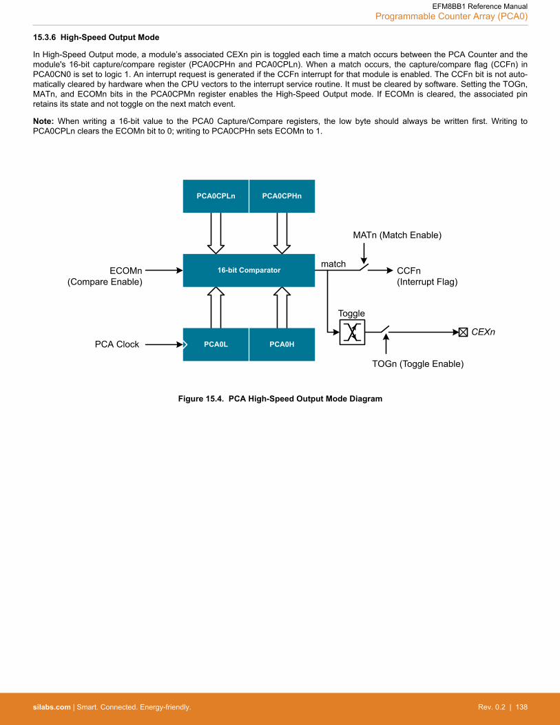
15.3.6 High-Speed Output Mode
In High-Speed Output mode, a module’s associated CEXn pin is toggled each time a match occurs between the PCA Counter and themodule's 16-bit capture/compare register (PCA0CPHn and PCA0CPLn). When a match occurs, the capture/compare flag (CCFn) inPCA0CN0 is set to logic 1. An interrupt request is generated if the CCFn interrupt for that module is enabled. The CCFn bit is not auto-matically cleared by hardware when the CPU vectors to the interrupt service routine. It must be cleared by software. Setting the TOGn,MATn, and ECOMn bits in the PCA0CPMn register enables the High-Speed Output mode. If ECOMn is cleared, the associated pinretains its state and not toggle on the next match event.
Note: When writing a 16-bit value to the PCA0 Capture/Compare registers, the low byte should always be written first. Writing toPCA0CPLn clears the ECOMn bit to 0; writing to PCA0CPHn sets ECOMn to 1.
PCA0L
PCA0CPLn
PCA0H
PCA0CPHn
ECOMn (Compare Enable)
PCA Clock
16-bit Comparatormatch
CCFn(Interrupt Flag)
MATn (Match Enable)
Toggle
TOGn (Toggle Enable)
CEXn
Figure 15.4. PCA High-Speed Output Mode Diagram
EFM8BB1 Reference ManualProgrammable Counter Array (PCA0)
silabs.com | Smart. Connected. Energy-friendly. Rev. 0.2 | 138
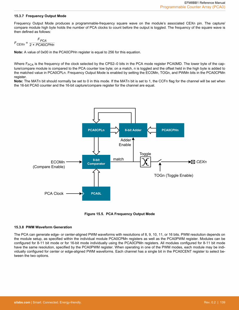
15.3.7 Frequency Output Mode
Frequency Output Mode produces a programmable-frequency square wave on the module’s associated CEXn pin. The capture/compare module high byte holds the number of PCA clocks to count before the output is toggled. The frequency of the square wave isthen defined as follows:
FCEXn =FPCA
2 × PCA0CPHn
Note: A value of 0x00 in the PCA0CPHn register is equal to 256 for this equation.
Where FPCA is the frequency of the clock selected by the CPS2–0 bits in the PCA mode register PCA0MD. The lower byte of the cap-ture/compare module is compared to the PCA counter low byte; on a match, n is toggled and the offset held in the high byte is added tothe matched value in PCA0CPLn. Frequency Output Mode is enabled by setting the ECOMn, TOGn, and PWMn bits in the PCA0CPMnregister.Note: The MATn bit should normally be set to 0 in this mode. If the MATn bit is set to 1, the CCFn flag for the channel will be set whenthe 16-bit PCA0 counter and the 16-bit capture/compare register for the channel are equal.
PCA0L
ECOMn (Compare Enable)
PCA Clock
8-bit Comparator
matchToggle
TOGn (Toggle Enable)
CEXn
8-bit Adder
Adder Enable
PCA0CPLn PCA0CPHn
Figure 15.5. PCA Frequency Output Mode
15.3.8 PWM Waveform Generation
The PCA can generate edge- or center-aligned PWM waveforms with resolutions of 8, 9, 10, 11, or 16 bits. PWM resolution depends onthe module setup, as specified within the individual module PCA0CPMn registers as well as the PCA0PWM register. Modules can beconfigured for 8-11 bit mode or for 16-bit mode individually using the PCA0CPMn registers. All modules configured for 8-11 bit modehave the same resolution, specified by the PCA0PWM register. When operating in one of the PWM modes, each module may be indi-vidually configured for center or edge-aligned PWM waveforms. Each channel has a single bit in the PCA0CENT register to select be-tween the two options.
EFM8BB1 Reference ManualProgrammable Counter Array (PCA0)
silabs.com | Smart. Connected. Energy-friendly. Rev. 0.2 | 139
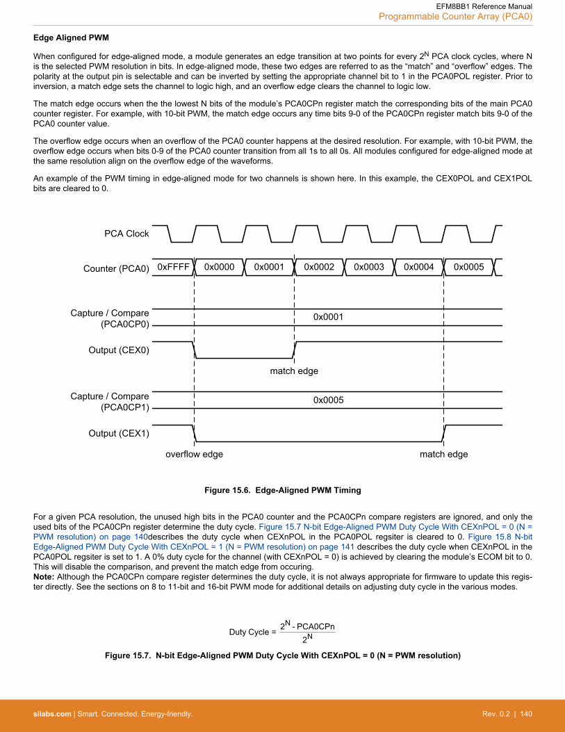
Edge Aligned PWM
When configured for edge-aligned mode, a module generates an edge transition at two points for every 2N PCA clock cycles, where Nis the selected PWM resolution in bits. In edge-aligned mode, these two edges are referred to as the “match” and “overflow” edges. Thepolarity at the output pin is selectable and can be inverted by setting the appropriate channel bit to 1 in the PCA0POL register. Prior toinversion, a match edge sets the channel to logic high, and an overflow edge clears the channel to logic low.
The match edge occurs when the the lowest N bits of the module’s PCA0CPn register match the corresponding bits of the main PCA0counter register. For example, with 10-bit PWM, the match edge occurs any time bits 9-0 of the PCA0CPn register match bits 9-0 of thePCA0 counter value.
The overflow edge occurs when an overflow of the PCA0 counter happens at the desired resolution. For example, with 10-bit PWM, theoverflow edge occurs when bits 0-9 of the PCA0 counter transition from all 1s to all 0s. All modules configured for edge-aligned mode atthe same resolution align on the overflow edge of the waveforms.
An example of the PWM timing in edge-aligned mode for two channels is shown here. In this example, the CEX0POL and CEX1POLbits are cleared to 0.
0xFFFF 0x0000 0x0001 0x0002 0x0003 0x0004 0x0005Counter (PCA0)
0x0001Capture / Compare (PCA0CP0)
Output (CEX0)
PCA Clock
match edge
overflow edge
0x0005Capture / Compare (PCA0CP1)
Output (CEX1)
match edge
Figure 15.6. Edge-Aligned PWM Timing
For a given PCA resolution, the unused high bits in the PCA0 counter and the PCA0CPn compare registers are ignored, and only theused bits of the PCA0CPn register determine the duty cycle. Figure 15.7 N-bit Edge-Aligned PWM Duty Cycle With CEXnPOL = 0 (N =PWM resolution) on page 140describes the duty cycle when CEXnPOL in the PCA0POL regsiter is cleared to 0. Figure 15.8 N-bitEdge-Aligned PWM Duty Cycle With CEXnPOL = 1 (N = PWM resolution) on page 141 describes the duty cycle when CEXnPOL in thePCA0POL regsiter is set to 1. A 0% duty cycle for the channel (with CEXnPOL = 0) is achieved by clearing the module’s ECOM bit to 0.This will disable the comparison, and prevent the match edge from occuring.Note: Although the PCA0CPn compare register determines the duty cycle, it is not always appropriate for firmware to update this regis-ter directly. See the sections on 8 to 11-bit and 16-bit PWM mode for additional details on adjusting duty cycle in the various modes.
Duty Cycle = 2N - PCA0CPn2N
Figure 15.7. N-bit Edge-Aligned PWM Duty Cycle With CEXnPOL = 0 (N = PWM resolution)
EFM8BB1 Reference ManualProgrammable Counter Array (PCA0)
silabs.com | Smart. Connected. Energy-friendly. Rev. 0.2 | 140

Duty Cycle = PCA0CPn2N
Figure 15.8. N-bit Edge-Aligned PWM Duty Cycle With CEXnPOL = 1 (N = PWM resolution)
EFM8BB1 Reference ManualProgrammable Counter Array (PCA0)
silabs.com | Smart. Connected. Energy-friendly. Rev. 0.2 | 141

Center Aligned PWM
When configured for center-aligned mode, a module generates an edge transition at two points for every 2(N+1) PCA clock cycles,where N is the selected PWM resolution in bits. In center-aligned mode, these two edges are referred to as the “up” and “down” edges.The polarity at the output pin is selectable and can be inverted by setting the appropriate channel bit to 1 in the PCA0POL register.
The generated waveforms are centered about the points where the lower N bits of the PCA0 counter are zero. The (N+1)th bit in thePCA0 counter acts as a selection between up and down edges. In 16-bit mode, a special 17th bit is implemented internally for thispurpose. At the center point, the (non-inverted) channel output is low when the (N+1)th bit is 0 and high when the (N+1)th bit is 1, exceptfor cases of 0% and 100% duty cycle. Prior to inversion, an up edge sets the channel to logic high, and a down edge clears the channelto logic low.
Down edges occur when the (N+1)th bit in the PCA0 counter is one and a logical inversion of the value in the module’s PCA0CPn regis-ter matches the main PCA0 counter register for the lowest N bits. For example, with 10-bit PWM, the down edge occurs when the one’scomplement of bits 9-0 of the PCA0CPn register match bits 9-0 of the PCA0 counter and bit 10 of the PCA0 counter is 1.
Up edges occur when the (N+1)th bit in the PCA0 counter is zero and the lowest N bits of the module’s PCA0CPn register match thevalue of (PCA0 - 1). For example, with 10-bit PWM, the up edge occurs when bits 9-0 of the PCA0CPn register are one less than bits9-0 of the PCA0 counter and bit 10 of the PCA0 counter is 0.
An example of the PWM timing in center-aligned mode for two channels is shown here. In this example, the CEX0POL and CEX1POLbits are cleared to 0.
0xFB 0xFC 0xFD 0xFE 0xFF 0x00 0x01 0x02 0x03 0x04Counter (PCA0L)
0x01Capture / Compare (PCA0CPL0)
Output (CEX0)
PCA Clock
down edge
0x04Capture / Compare (PCA0CPL1)
Output (CEX1)
up edge
down edge up edge
center
center
center
Figure 15.9. Center-Aligned PWM Timing
Figure 15.10 N-bit Center-Aligned PWM Duty Cycle With CEXnPOL = 0 (N = PWM resolution) on page 143 describes the duty cyclewhen CEXnPOL in the PCA0POL regsiter is cleared to 0. Figure 15.11 N-bit Center-Aligned PWM Duty Cycle With CEXnPOL = 1 (N =PWM resolution) on page 143 describes the duty cycle when CEXnPOL in the PCA0POL regsiter is set to 1. The equations are trueonly when the lowest N bits of the PCA0CPn register are not all 0s or all 1s. With CEXnPOL equal to zero, 100% duty cycle is producedwhen the lowest N bits of PCA0CPn are all 0, and 0% duty cycle is produced when the lowest N bits of PCA0CPn are all 1. For a givenPCA resolution, the unused high bits in the PCA0 counter and the PCA0CPn compare registers are ignored, and only the used bits ofthe PCA0CPn register determine the duty cycle.
Note: Although the PCA0CPn compare register determines the duty cycle, it is not always appropriate for firmware to update this regis-ter directly. See the sections on 8 to 11-bit and 16-bit PWM mode for additional details on adjusting duty cycle in the various modes.
EFM8BB1 Reference ManualProgrammable Counter Array (PCA0)
silabs.com | Smart. Connected. Energy-friendly. Rev. 0.2 | 142

Duty Cycle =2N - PCA0CPn - 1
22N
Figure 15.10. N-bit Center-Aligned PWM Duty Cycle With CEXnPOL = 0 (N = PWM resolution)
Duty Cycle =PCA0CPn + 1
22N
Figure 15.11. N-bit Center-Aligned PWM Duty Cycle With CEXnPOL = 1 (N = PWM resolution)
15.3.8.1 8 to 11-Bit PWM Modes
Each module can be used independently to generate a pulse width modulated (PWM) output on its associated CEXn pin. The frequen-cy of the output is dependent on the timebase for the PCA counter/timer and the setting of the PWM cycle length (8 through 11-bits).For backwards-compatibility with the 8-bit PWM mode available on other devices, the 8-bit PWM mode operates slightly different than 9through 11-bit PWM modes.
Important: All channels configured for 8 to 11-bit PWM mode use the same cycle length. It is not possible to configure one channel for8-bit PWM mode and another for 11-bit mode (for example). However, other PCA channels can be configured to Pin Capture, High-Speed Output, Software Timer, Frequency Output, or 16-bit PWM mode independently. Each channel configured for a PWM mode canbe individually selected to operate in edge-aligned or center-aligned mode.
8-bit Pulse Width Modulator Mode
In 8-bit PWM mode, the duty cycle is determined by the value of the low byte of the PCA0CPn register (PCA0CPLn). To adjust the dutycycle, PCA0CPLn should not normally be written directly. Instead, the recommendation is to adjust the duty cycle using the high byte ofthe PCA0CPn register (register PCA0CPHn). This allows seamless updating of the PWM waveform as PCA0CPLn is reloaded auto-matically with the value stored in PCA0CPHn during the overflow edge (in edge-aligned mode) or the up edge (in center-aligned mode).
Setting the ECOMn and PWMn bits in the PCA0CPMn register and setting the CLSEL bits in register PCA0PWM to 00b enables 8-Bitpulse width modulator mode. If the MATn bit is set to 1, the CCFn flag for the module is set each time a match edge or up edge occurs.The COVF flag in PCA0PWM can be used to detect the overflow (falling edge), which occurs every 256 PCA clock cycles.
9- to 11-bit Pulse Width Modulator Mode
In 9 to 11-bit PWM mode, the duty cycle is determined by the value of the least significant N bits of the PCA0CPn register, where N isthe selected PWM resolution.
To adjust the duty cycle, PCA0CPn should not normally be written directly. Instead, the recommendation is to adjust the duty cycle bywriting to an “Auto-Reload” register, which is dual-mapped into the PCA0CPHn and PCA0CPLn register locations. The data written todefine the duty cycle should be right-justified in the registers. The auto-reload registers are accessed (read or written) when the bit AR-SEL in PCA0PWM is set to 1. The capture/compare registers are accessed when ARSEL is set to 0. This allows seamless updating ofthe PWM waveform, as the PCA0CPn register is reloaded automatically with the value stored in the auto-reload registers during theoverflow edge (in edge-aligned mode) or the up edge (in center-aligned mode).
Setting the ECOMn and PWMn bits in the PCA0CPMn register and setting the CLSEL bits in register PCA0PWM to 00b enables 8-Bitpulse width modulator mode. If the MATn bit is set to 1, the CCFn flag for the module is set each time a match edge or up edge occurs.The COVF flag in PCA0PWM can be used to detect the overflow or down edge.
The 9 to 11-bit PWM mode is selected by setting the ECOMn and PWMn bits in the PCA0CPMn register and setting the CLSEL bits inregister PCA0PWM to the desired cycle length (other than 8-bits). If the MATn bit is set to 1, the CCFn flag for the module is set eachtime a match edge or up edge occurs. The COVF flag in PCA0PWM can be used to detect the overflow or down edge.
Important: When writing a 16-bit value to the PCA0CPn registers, the low byte should always be written first. Writing to PCA0CPLnclears the ECOMn bit to 0; writing to PCA0CPHn sets ECOMn to 1.
EFM8BB1 Reference ManualProgrammable Counter Array (PCA0)
silabs.com | Smart. Connected. Energy-friendly. Rev. 0.2 | 143

15.3.8.2 16-Bit PWM Mode
A PCA module may also be operated in 16-Bit PWM mode. 16-bit PWM mode is independent of the other PWM modes. The entirePCA0CP register is used to determine the duty cycle in 16-bit PWM mode.
To output a varying duty cycle, new value writes should be synchronized with the PCA CCFn match flag to ensure seamless updates.
16-Bit PWM mode is enabled by setting the ECOMn, PWMn, and PWM16n bits in the PCA0CPMn register. For a varying duty cycle,the match interrupt flag should be enabled (ECCFn = 1 AND MATn = 1) to help synchronize the capture/compare register writes. If theMATn bit is set to 1, the CCFn flag for the module is set each time a match edge or up edge occurs. The CF flag in PCA0CN0 can beused to detect the overflow or down edge.Important: When writing a 16-bit value to the PCA0 Capture/Compare registers, the low byte should always be written first. Writing toPCA0CPLn clears the ECOMn bit to 0; writing to PCA0CPHn sets ECOMn to 1.
EFM8BB1 Reference ManualProgrammable Counter Array (PCA0)
silabs.com | Smart. Connected. Energy-friendly. Rev. 0.2 | 144

15.3.8.3 Comparator Clear Function
In 8/9/10/11/16-bit PWM modes, the comparator clear function utilizes the Comparator0 output synchronized to the system clock toclear CEXn to logic low for the current PWM cycle. This comparator clear function can be enabled for each PWM channel by setting theCPCEn bits to 1 in the PCA0CLR SFR. When the comparator clear function is disabled, CEXn is unaffected.
The asynchronous Comparator 0 output is logic high when the voltage of CP0+ is greater than CP0– and logic low when the voltage ofCP0+ is less than CP0–. The polarity of the Comparator 0 output is used to clear CEXn as follows: when CPCPOL = 0, CEXn is clearedon the falling edge of the Comparator0 output.
CEXn (CPCEn = 0)
CEXn (CPCEn = 1)
Comparator0 Output (CPCPOL = 0)
Figure 15.12. CEXn with CPCEn = 1, CPCPOL = 0
When CPCPOL = 1, CEXn is cleared on the rising edge of the Comparator0 output.
CEXn (CPCEn = 0)
CEXn (CPCEn = 1)
Comparator0 Output (CPCPOL = 1)
Figure 15.13. CEXn with CPCEn = 1, CPCPOL = 1
In the PWM cycle following the current cycle, should the Comparator 0 output remain logic low when CPCPOL = 0 or logic high whenCPCPOL = 1, CEXn will continue to be cleared.
CEXn (CPCEn = 0)
CEXn (CPCEn = 1)
Comparator0 Output (CPCPOL = 0)
Figure 15.14. CEXn with CPCEn = 1, CPCPOL = 0
EFM8BB1 Reference ManualProgrammable Counter Array (PCA0)
silabs.com | Smart. Connected. Energy-friendly. Rev. 0.2 | 145
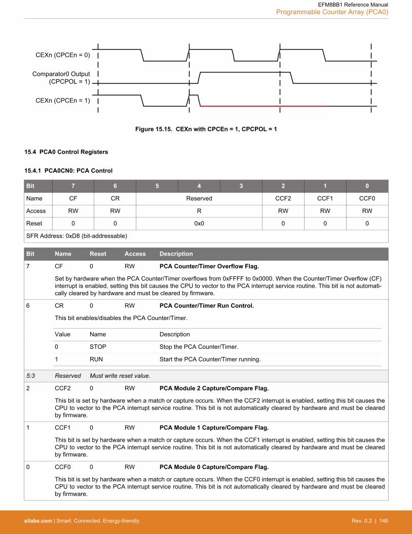
CEXn (CPCEn = 0)
CEXn (CPCEn = 1)
Comparator0 Output (CPCPOL = 1)
Figure 15.15. CEXn with CPCEn = 1, CPCPOL = 1
15.4 PCA0 Control Registers
15.4.1 PCA0CN0: PCA Control
Bit 7 6 5 4 3 2 1 0
Name CF CR Reserved CCF2 CCF1 CCF0
Access RW RW R RW RW RW
Reset 0 0 0x0 0 0 0
SFR Address: 0xD8 (bit-addressable)
Bit Name Reset Access Description
7 CF 0 RW PCA Counter/Timer Overflow Flag.
Set by hardware when the PCA Counter/Timer overflows from 0xFFFF to 0x0000. When the Counter/Timer Overflow (CF)interrupt is enabled, setting this bit causes the CPU to vector to the PCA interrupt service routine. This bit is not automati-cally cleared by hardware and must be cleared by firmware.
6 CR 0 RW PCA Counter/Timer Run Control.
This bit enables/disables the PCA Counter/Timer.
Value Name Description
0 STOP Stop the PCA Counter/Timer.
1 RUN Start the PCA Counter/Timer running.
5:3 Reserved Must write reset value.
2 CCF2 0 RW PCA Module 2 Capture/Compare Flag.
This bit is set by hardware when a match or capture occurs. When the CCF2 interrupt is enabled, setting this bit causes theCPU to vector to the PCA interrupt service routine. This bit is not automatically cleared by hardware and must be clearedby firmware.
1 CCF1 0 RW PCA Module 1 Capture/Compare Flag.
This bit is set by hardware when a match or capture occurs. When the CCF1 interrupt is enabled, setting this bit causes theCPU to vector to the PCA interrupt service routine. This bit is not automatically cleared by hardware and must be clearedby firmware.
0 CCF0 0 RW PCA Module 0 Capture/Compare Flag.
This bit is set by hardware when a match or capture occurs. When the CCF0 interrupt is enabled, setting this bit causes theCPU to vector to the PCA interrupt service routine. This bit is not automatically cleared by hardware and must be clearedby firmware.
EFM8BB1 Reference ManualProgrammable Counter Array (PCA0)
silabs.com | Smart. Connected. Energy-friendly. Rev. 0.2 | 146

15.4.2 PCA0MD: PCA Mode
Bit 7 6 5 4 3 2 1 0
Name CIDL Reserved CPS ECF
Access RW R RW RW
Reset 0 0x0 0x0 0
SFR Address: 0xD9
Bit Name Reset Access Description
7 CIDL 0 RW PCA Counter/Timer Idle Control.
Specifies PCA behavior when CPU is in Idle Mode.
Value Name Description
0 NORMAL PCA continues to function normally while the system controller is in Idle Mode.
1 SUSPEND PCA operation is suspended while the system controller is in Idle Mode.
6:4 Reserved Must write reset value.
3:1 CPS 0x0 RW PCA Counter/Timer Pulse Select.
These bits select the timebase source for the PCA counter.
Value Name Description
0x0 SYSCLK_DIV_12 System clock divided by 12.
0x1 SYSCLK_DIV_4 System clock divided by 4.
0x2 T0_OVERFLOW Timer 0 overflow.
0x3 ECI High-to-low transitions on ECI (max rate = system clock divided by 4).
0x4 SYSCLK System clock.
0x5 EXTOSC_DIV_8 External clock divided by 8 (synchronized with the system clock).
0x6 LFOSC_DIV_8 Low frequency oscillator divided by 8.
0 ECF 0 RW PCA Counter/Timer Overflow Interrupt Enable.
This bit sets the masking of the PCA Counter/Timer Overflow (CF) interrupt.
Value Name Description
0 OVF_INT_DISABLED Disable the CF interrupt.
1 OVF_INT_ENABLED Enable a PCA Counter/Timer Overflow interrupt request when CF is set.
EFM8BB1 Reference ManualProgrammable Counter Array (PCA0)
silabs.com | Smart. Connected. Energy-friendly. Rev. 0.2 | 147

15.4.3 PCA0PWM: PCA PWM Configuration
Bit 7 6 5 4 3 2 1 0
Name ARSEL ECOV COVF Reserved CLSEL
Access RW RW RW R RW
Reset 0 0 0 0x0 0x0
SFR Address: 0xF7
Bit Name Reset Access Description
7 ARSEL 0 RW Auto-Reload Register Select.
This bit selects whether to read and write the normal PCA capture/compare registers (PCA0CPn), or the Auto-Reload reg-isters at the same SFR addresses. This function is used to define the reload value for 9 to 11-bit PWM modes. In all othermodes, the Auto-Reload registers have no function.
Value Name Description
0 CAPTURE_COMPARE Read/Write Capture/Compare Registers at PCA0CPHn and PCA0CPLn.
1 AUTORELOAD Read/Write Auto-Reload Registers at PCA0CPHn and PCA0CPLn.
6 ECOV 0 RW Cycle Overflow Interrupt Enable.
This bit sets the masking of the Cycle Overflow Flag (COVF) interrupt.
Value Name Description
0 COVF_MASK_DISA-BLED
COVF will not generate PCA interrupts.
1 COVF_MASK_ENA-BLED
A PCA interrupt will be generated when COVF is set.
5 COVF 0 RW Cycle Overflow Flag.
This bit indicates an overflow of the 8th to 11th bit of the main PCA counter (PCA0). The specific bit used for this flag de-pends on the setting of the Cycle Length Select bits. The bit can be set by hardware or firmware, but must be cleared byfirmware.
Value Name Description
0 NO_OVERFLOW No overflow has occurred since the last time this bit was cleared.
1 OVERFLOW An overflow has occurred since the last time this bit was cleared.
4:3 Reserved Must write reset value.
2:0 CLSEL 0x0 RW Cycle Length Select.
When 16-bit PWM mode is not selected, these bits select the length of the PWM cycle. This affects all channels configuredfor PWM which are not using 16-bit PWM mode. These bits are ignored for individual channels configured to 16-bit PWMmode.
Value Name Description
0x0 8_BITS 8 bits.
0x1 9_BITS 9 bits.
0x2 10_BITS 10 bits.
0x3 11_BITS 11 bits.
EFM8BB1 Reference ManualProgrammable Counter Array (PCA0)
silabs.com | Smart. Connected. Energy-friendly. Rev. 0.2 | 148

15.4.4 PCA0CLR: PCA Comparator Clear Control
Bit 7 6 5 4 3 2 1 0
Name CPCPOL Reserved CPCE2 CPCE1 CPCE0
Access RW R RW RW RW
Reset 0 0x0 0 0 0
SFR Address: 0x9C
Bit Name Reset Access Description
7 CPCPOL 0 RW Comparator Clear Polarity.
Selects the polarity of the comparator result that will clear the PCA channel(s).
Value Name Description
0 LOW PCA channel(s) will be cleared when comparator result goes logic low.
1 HIGH PCA channel(s) will be cleared when comparator result goes logic high.
6:3 Reserved Must write reset value.
2 CPCE2 0 RW Comparator Clear Enable for CEX2.
Enables the comparator clear function on PCA channel 2.
1 CPCE1 0 RW Comparator Clear Enable for CEX1.
Enables the comparator clear function on PCA channel 1.
0 CPCE0 0 RW Comparator Clear Enable for CEX0.
Enables the comparator clear function on PCA channel 0.
15.4.5 PCA0L: PCA Counter/Timer Low Byte
Bit 7 6 5 4 3 2 1 0
Name PCA0L
Access RW
Reset 0x00
SFR Address: 0xF9
Bit Name Reset Access Description
7:0 PCA0L 0x00 RW PCA Counter/Timer Low Byte.
The PCA0L register holds the low byte (LSB) of the 16-bit PCA Counter/Timer.
EFM8BB1 Reference ManualProgrammable Counter Array (PCA0)
silabs.com | Smart. Connected. Energy-friendly. Rev. 0.2 | 149
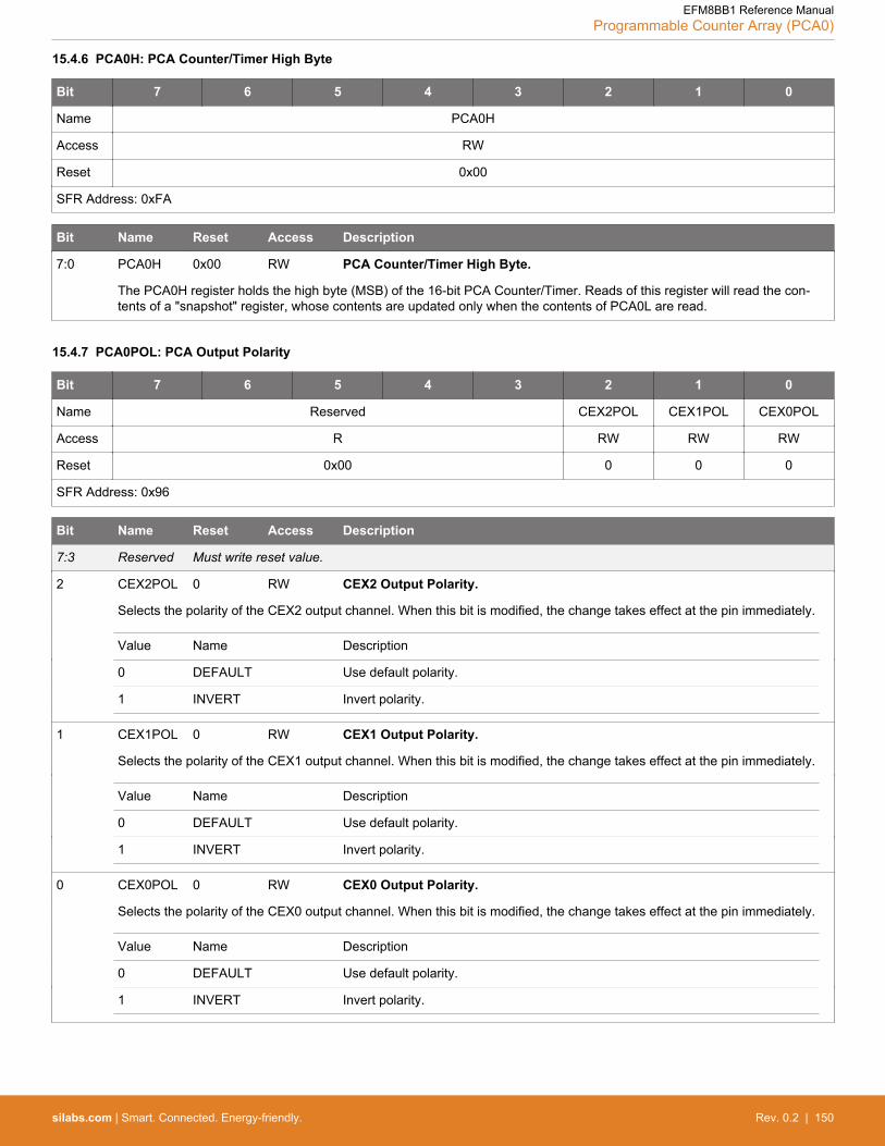
15.4.6 PCA0H: PCA Counter/Timer High Byte
Bit 7 6 5 4 3 2 1 0
Name PCA0H
Access RW
Reset 0x00
SFR Address: 0xFA
Bit Name Reset Access Description
7:0 PCA0H 0x00 RW PCA Counter/Timer High Byte.
The PCA0H register holds the high byte (MSB) of the 16-bit PCA Counter/Timer. Reads of this register will read the con-tents of a "snapshot" register, whose contents are updated only when the contents of PCA0L are read.
15.4.7 PCA0POL: PCA Output Polarity
Bit 7 6 5 4 3 2 1 0
Name Reserved CEX2POL CEX1POL CEX0POL
Access R RW RW RW
Reset 0x00 0 0 0
SFR Address: 0x96
Bit Name Reset Access Description
7:3 Reserved Must write reset value.
2 CEX2POL 0 RW CEX2 Output Polarity.
Selects the polarity of the CEX2 output channel. When this bit is modified, the change takes effect at the pin immediately.
Value Name Description
0 DEFAULT Use default polarity.
1 INVERT Invert polarity.
1 CEX1POL 0 RW CEX1 Output Polarity.
Selects the polarity of the CEX1 output channel. When this bit is modified, the change takes effect at the pin immediately.
Value Name Description
0 DEFAULT Use default polarity.
1 INVERT Invert polarity.
0 CEX0POL 0 RW CEX0 Output Polarity.
Selects the polarity of the CEX0 output channel. When this bit is modified, the change takes effect at the pin immediately.
Value Name Description
0 DEFAULT Use default polarity.
1 INVERT Invert polarity.
EFM8BB1 Reference ManualProgrammable Counter Array (PCA0)
silabs.com | Smart. Connected. Energy-friendly. Rev. 0.2 | 150
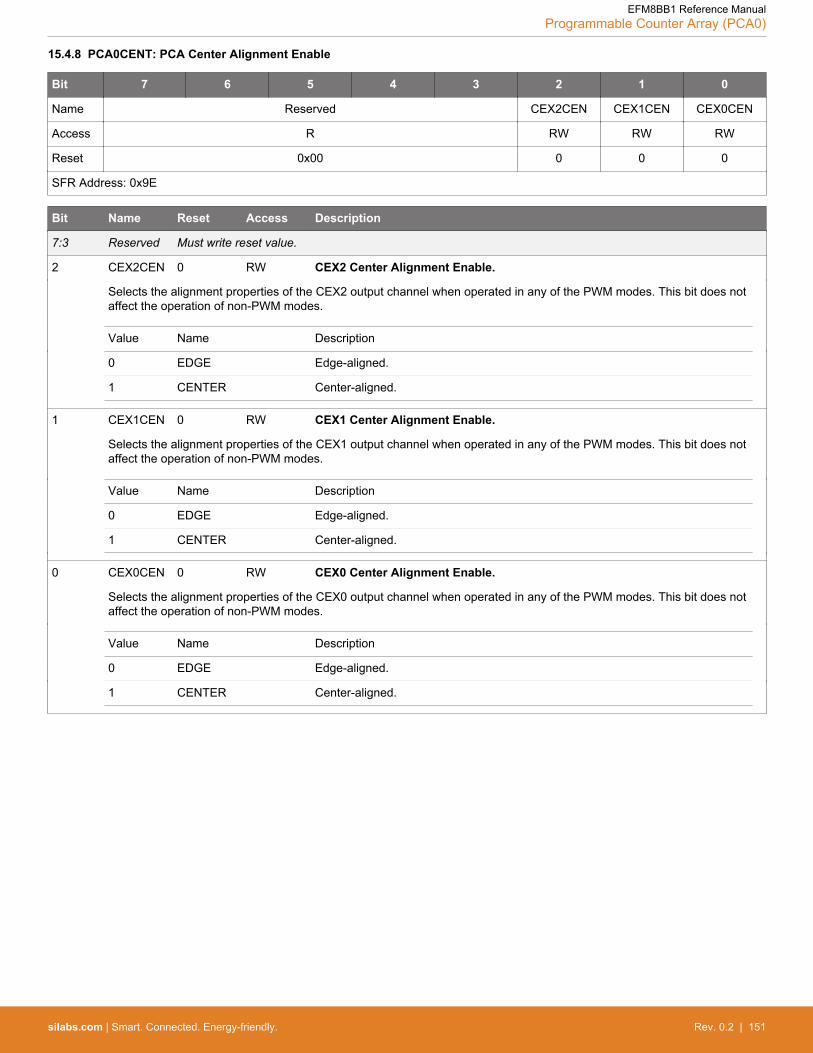
15.4.8 PCA0CENT: PCA Center Alignment Enable
Bit 7 6 5 4 3 2 1 0
Name Reserved CEX2CEN CEX1CEN CEX0CEN
Access R RW RW RW
Reset 0x00 0 0 0
SFR Address: 0x9E
Bit Name Reset Access Description
7:3 Reserved Must write reset value.
2 CEX2CEN 0 RW CEX2 Center Alignment Enable.
Selects the alignment properties of the CEX2 output channel when operated in any of the PWM modes. This bit does notaffect the operation of non-PWM modes.
Value Name Description
0 EDGE Edge-aligned.
1 CENTER Center-aligned.
1 CEX1CEN 0 RW CEX1 Center Alignment Enable.
Selects the alignment properties of the CEX1 output channel when operated in any of the PWM modes. This bit does notaffect the operation of non-PWM modes.
Value Name Description
0 EDGE Edge-aligned.
1 CENTER Center-aligned.
0 CEX0CEN 0 RW CEX0 Center Alignment Enable.
Selects the alignment properties of the CEX0 output channel when operated in any of the PWM modes. This bit does notaffect the operation of non-PWM modes.
Value Name Description
0 EDGE Edge-aligned.
1 CENTER Center-aligned.
EFM8BB1 Reference ManualProgrammable Counter Array (PCA0)
silabs.com | Smart. Connected. Energy-friendly. Rev. 0.2 | 151
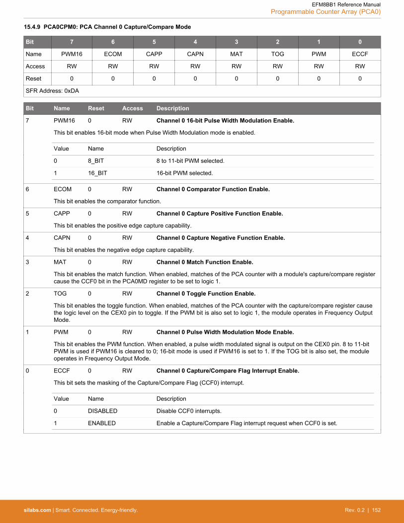
15.4.9 PCA0CPM0: PCA Channel 0 Capture/Compare Mode
Bit 7 6 5 4 3 2 1 0
Name PWM16 ECOM CAPP CAPN MAT TOG PWM ECCF
Access RW RW RW RW RW RW RW RW
Reset 0 0 0 0 0 0 0 0
SFR Address: 0xDA
Bit Name Reset Access Description
7 PWM16 0 RW Channel 0 16-bit Pulse Width Modulation Enable.
This bit enables 16-bit mode when Pulse Width Modulation mode is enabled.
Value Name Description
0 8_BIT 8 to 11-bit PWM selected.
1 16_BIT 16-bit PWM selected.
6 ECOM 0 RW Channel 0 Comparator Function Enable.
This bit enables the comparator function.
5 CAPP 0 RW Channel 0 Capture Positive Function Enable.
This bit enables the positive edge capture capability.
4 CAPN 0 RW Channel 0 Capture Negative Function Enable.
This bit enables the negative edge capture capability.
3 MAT 0 RW Channel 0 Match Function Enable.
This bit enables the match function. When enabled, matches of the PCA counter with a module's capture/compare registercause the CCF0 bit in the PCA0MD register to be set to logic 1.
2 TOG 0 RW Channel 0 Toggle Function Enable.
This bit enables the toggle function. When enabled, matches of the PCA counter with the capture/compare register causethe logic level on the CEX0 pin to toggle. If the PWM bit is also set to logic 1, the module operates in Frequency OutputMode.
1 PWM 0 RW Channel 0 Pulse Width Modulation Mode Enable.
This bit enables the PWM function. When enabled, a pulse width modulated signal is output on the CEX0 pin. 8 to 11-bitPWM is used if PWM16 is cleared to 0; 16-bit mode is used if PWM16 is set to 1. If the TOG bit is also set, the moduleoperates in Frequency Output Mode.
0 ECCF 0 RW Channel 0 Capture/Compare Flag Interrupt Enable.
This bit sets the masking of the Capture/Compare Flag (CCF0) interrupt.
Value Name Description
0 DISABLED Disable CCF0 interrupts.
1 ENABLED Enable a Capture/Compare Flag interrupt request when CCF0 is set.
EFM8BB1 Reference ManualProgrammable Counter Array (PCA0)
silabs.com | Smart. Connected. Energy-friendly. Rev. 0.2 | 152

15.4.10 PCA0CPL0: PCA Channel 0 Capture Module Low Byte
Bit 7 6 5 4 3 2 1 0
Name PCA0CPL0
Access RW
Reset 0x00
SFR Address: 0xFB
Bit Name Reset Access Description
7:0 PCA0CPL0 0x00 RW PCA Channel 0 Capture Module Low Byte.
The PCA0CPL0 register holds the low byte (LSB) of the 16-bit capture module. This register address also allows access tothe low byte of the corresponding PCA channel's auto-reload value for 9 to 11-bit PWM mode. The ARSEL bit in registerPCA0PWM controls which register is accessed.
A write to this register will clear the module's ECOM bit to a 0.
15.4.11 PCA0CPH0: PCA Channel 0 Capture Module High Byte
Bit 7 6 5 4 3 2 1 0
Name PCA0CPH0
Access RW
Reset 0x00
SFR Address: 0xFC
Bit Name Reset Access Description
7:0 PCA0CPH0
0x00 RW PCA Channel 0 Capture Module High Byte.
The PCA0CPH0 register holds the high byte (MSB) of the 16-bit capture module. This register address also allows accessto the high byte of the corresponding PCA channel's auto-reload value for 9 to 11-bit PWM mode. The ARSEL bit in registerPCA0PWM controls which register is accessed.
A write to this register will set the module's ECOM bit to a 1.
EFM8BB1 Reference ManualProgrammable Counter Array (PCA0)
silabs.com | Smart. Connected. Energy-friendly. Rev. 0.2 | 153

15.4.12 PCA0CPM1: PCA Channel 1 Capture/Compare Mode
Bit 7 6 5 4 3 2 1 0
Name PWM16 ECOM CAPP CAPN MAT TOG PWM ECCF
Access RW RW RW RW RW RW RW RW
Reset 0 0 0 0 0 0 0 0
SFR Address: 0xDB
Bit Name Reset Access Description
7 PWM16 0 RW Channel 1 16-bit Pulse Width Modulation Enable.
This bit enables 16-bit mode when Pulse Width Modulation mode is enabled.
Value Name Description
0 8_BIT 8 to 11-bit PWM selected.
1 16_BIT 16-bit PWM selected.
6 ECOM 0 RW Channel 1 Comparator Function Enable.
This bit enables the comparator function.
5 CAPP 0 RW Channel 1 Capture Positive Function Enable.
This bit enables the positive edge capture capability.
4 CAPN 0 RW Channel 1 Capture Negative Function Enable.
This bit enables the negative edge capture capability.
3 MAT 0 RW Channel 1 Match Function Enable.
This bit enables the match function. When enabled, matches of the PCA counter with a module's capture/compare registercause the CCF1 bit in the PCA0MD register to be set to logic 1.
2 TOG 0 RW Channel 1 Toggle Function Enable.
This bit enables the toggle function. When enabled, matches of the PCA counter with the capture/compare register causethe logic level on the CEX1 pin to toggle. If the PWM bit is also set to logic 1, the module operates in Frequency OutputMode.
1 PWM 0 RW Channel 1 Pulse Width Modulation Mode Enable.
This bit enables the PWM function. When enabled, a pulse width modulated signal is output on the CEX1 pin. 8 to 11-bitPWM is used if PWM16 is cleared to 0; 16-bit mode is used if PWM16 is set to 1. If the TOG bit is also set, the moduleoperates in Frequency Output Mode.
0 ECCF 0 RW Channel 1 Capture/Compare Flag Interrupt Enable.
This bit sets the masking of the Capture/Compare Flag (CCF1) interrupt.
Value Name Description
0 DISABLED Disable CCF1 interrupts.
1 ENABLED Enable a Capture/Compare Flag interrupt request when CCF1 is set.
EFM8BB1 Reference ManualProgrammable Counter Array (PCA0)
silabs.com | Smart. Connected. Energy-friendly. Rev. 0.2 | 154

15.4.13 PCA0CPL1: PCA Channel 1 Capture Module Low Byte
Bit 7 6 5 4 3 2 1 0
Name PCA0CPL1
Access RW
Reset 0x00
SFR Address: 0xE9
Bit Name Reset Access Description
7:0 PCA0CPL1 0x00 RW PCA Channel 1 Capture Module Low Byte.
The PCA0CPL1 register holds the low byte (LSB) of the 16-bit capture module. This register address also allows access tothe low byte of the corresponding PCA channel's auto-reload value for 9 to 11-bit PWM mode. The ARSEL bit in registerPCA0PWM controls which register is accessed.
A write to this register will clear the module's ECOM bit to a 0.
15.4.14 PCA0CPH1: PCA Channel 1 Capture Module High Byte
Bit 7 6 5 4 3 2 1 0
Name PCA0CPH1
Access RW
Reset 0x00
SFR Address: 0xEA
Bit Name Reset Access Description
7:0 PCA0CPH1
0x00 RW PCA Channel 1 Capture Module High Byte.
The PCA0CPH1 register holds the high byte (MSB) of the 16-bit capture module. This register address also allows accessto the high byte of the corresponding PCA channel's auto-reload value for 9 to 11-bit PWM mode. The ARSEL bit in registerPCA0PWM controls which register is accessed.
A write to this register will set the module's ECOM bit to a 1.
EFM8BB1 Reference ManualProgrammable Counter Array (PCA0)
silabs.com | Smart. Connected. Energy-friendly. Rev. 0.2 | 155

15.4.15 PCA0CPM2: PCA Channel 2 Capture/Compare Mode
Bit 7 6 5 4 3 2 1 0
Name PWM16 ECOM CAPP CAPN MAT TOG PWM ECCF
Access RW RW RW RW RW RW RW RW
Reset 0 0 0 0 0 0 0 0
SFR Address: 0xDC
Bit Name Reset Access Description
7 PWM16 0 RW Channel 2 16-bit Pulse Width Modulation Enable.
This bit enables 16-bit mode when Pulse Width Modulation mode is enabled.
Value Name Description
0 8_BIT 8 to 11-bit PWM selected.
1 16_BIT 16-bit PWM selected.
6 ECOM 0 RW Channel 2 Comparator Function Enable.
This bit enables the comparator function.
5 CAPP 0 RW Channel 2 Capture Positive Function Enable.
This bit enables the positive edge capture capability.
4 CAPN 0 RW Channel 2 Capture Negative Function Enable.
This bit enables the negative edge capture capability.
3 MAT 0 RW Channel 2 Match Function Enable.
This bit enables the match function. When enabled, matches of the PCA counter with a module's capture/compare registercause the CCF2 bit in the PCA0MD register to be set to logic 1.
2 TOG 0 RW Channel 2 Toggle Function Enable.
This bit enables the toggle function. When enabled, matches of the PCA counter with the capture/compare register causethe logic level on the CEX2 pin to toggle. If the PWM bit is also set to logic 1, the module operates in Frequency OutputMode.
1 PWM 0 RW Channel 2 Pulse Width Modulation Mode Enable.
This bit enables the PWM function. When enabled, a pulse width modulated signal is output on the CEX2 pin. 8 to 11-bitPWM is used if PWM16 is cleared to 0; 16-bit mode is used if PWM16 is set to 1. If the TOG bit is also set, the moduleoperates in Frequency Output Mode.
0 ECCF 0 RW Channel 2 Capture/Compare Flag Interrupt Enable.
This bit sets the masking of the Capture/Compare Flag (CCF2) interrupt.
Value Name Description
0 DISABLED Disable CCF2 interrupts.
1 ENABLED Enable a Capture/Compare Flag interrupt request when CCF2 is set.
EFM8BB1 Reference ManualProgrammable Counter Array (PCA0)
silabs.com | Smart. Connected. Energy-friendly. Rev. 0.2 | 156

15.4.16 PCA0CPL2: PCA Channel 2 Capture Module Low Byte
Bit 7 6 5 4 3 2 1 0
Name PCA0CPL2
Access RW
Reset 0x00
SFR Address: 0xEB
Bit Name Reset Access Description
7:0 PCA0CPL2 0x00 RW PCA Channel 2 Capture Module Low Byte.
The PCA0CPL2 register holds the low byte (LSB) of the 16-bit capture module. This register address also allows access tothe low byte of the corresponding PCA channel's auto-reload value for 9 to 11-bit PWM mode. The ARSEL bit in registerPCA0PWM controls which register is accessed.
A write to this register will clear the module's ECOM bit to a 0.
15.4.17 PCA0CPH2: PCA Channel 2 Capture Module High Byte
Bit 7 6 5 4 3 2 1 0
Name PCA0CPH2
Access RW
Reset 0x00
SFR Address: 0xEC
Bit Name Reset Access Description
7:0 PCA0CPH2
0x00 RW PCA Channel 2 Capture Module High Byte.
The PCA0CPH2 register holds the high byte (MSB) of the 16-bit capture module. This register address also allows accessto the high byte of the corresponding PCA channel's auto-reload value for 9 to 11-bit PWM mode. The ARSEL bit in registerPCA0PWM controls which register is accessed.
A write to this register will set the module's ECOM bit to a 1.
EFM8BB1 Reference ManualProgrammable Counter Array (PCA0)
silabs.com | Smart. Connected. Energy-friendly. Rev. 0.2 | 157

16. Serial Peripheral Interface (SPI0)
16.1 Introduction
The serial peripheral interface (SPI) module provides access to a flexible, full-duplex synchronous serial bus. The SPI can operate as amaster or slave device in both 3-wire or 4-wire modes, and supports multiple masters and slaves on a single SPI bus. The slave-select(NSS) signal can be configured as an input to select the SPI in slave mode, or to disable master mode operation in a multi-masterenvironment, avoiding contention on the SPI bus when more than one master attempts simultaneous data transfers. NSS can also beconfigured as a firmware-controlled chip-select output in master mode, or disabled to reduce the number of pins required. Additionalgeneral purpose port I/O pins can be used to select multiple slave devices in master mode.
SPI0
Shift RegisterMISO
MOSI
Clock Rate GeneratorSYSCLK Bus Control
Master or Slave
SCK Polarity
SCK Phase
NSS Control
SCK
NSS
SPI0DAT
TX Buffer RX Buffer
Figure 16.1. SPI Block Diagram
16.2 Features
The SPI module includes the following features:• Supports 3- or 4-wire operation in master or slave modes.• Supports external clock frequencies up to SYSCLK / 2 in master mode and SYSCLK / 10 in slave mode.• Support for four clock phase and polarity options.• 8-bit dedicated clock clock rate generator.• Support for multiple masters on the same data lines.
EFM8BB1 Reference ManualSerial Peripheral Interface (SPI0)
silabs.com | Smart. Connected. Energy-friendly. Rev. 0.2 | 158

16.3 Functional Description
16.3.1 Signals
The SPI interface consists of up to four signals: MOSI, MISO, SCK, and NSS.
Master Out, Slave In (MOSI): The MOSI signal is the data output pin when configured as a master device and the data input pin whenconfigured as a slave. It is used to serially transfer data from the master to the slave. Data is transferred on the MOSI pin most-signifi-cant bit first. When configured as a master, MOSI is driven from the internal shift register in both 3- and 4-wire mode.
Master In, Slave Out (MISO): The MISO signal is the data input pin when configured as a master device and the data output pin whenconfigured as a slave. It is used to serially transfer data from the slave to the master. Data is transferred on the MISO pin most-signifi-cant bit first. The MISO pin is placed in a high-impedance state when the SPI module is disabled or when the SPI operates in 4-wiremode as a slave that is not selected. When acting as a slave in 3-wire mode, MISO is always driven from the internal shift register.
Serial Clock (SCK): The SCK signal is an output from the master device and an input to slave devices. It is used to synchronize thetransfer of data between the master and slave on the MOSI and MISO lines. The SPI module generates this signal when operating as amaster and receives it as a slave. The SCK signal is ignored by a SPI slave when the slave is not selected in 4-wire slave mode.
Slave Select (NSS): The function of the slave-select (NSS) signal is dependent on the setting of the NSSMD bitfield. There are threepossible modes that can be selected with these bits:• NSSMD[1:0] = 00: 3-Wire Master or 3-Wire Slave Mode: The SPI operates in 3-wire mode, and NSS is disabled. When operating as
a slave device, the SPI is always selected in 3-wire mode. Since no select signal is present, the SPI must be the only slave on thebus in 3-wire mode. This is intended for point-to-point communication between a master and a single slave.
• NSSMD[1:0] = 01: 4-Wire Slave or Multi-Master Mode: The SPI operates in 4-wire mode, and NSS is configured as an input. Whenoperating as a slave, NSS selects the SPI device. When operating as a master, a 1-to- 0 transition of the NSS signal disables themaster function of the SPI module so that multiple master devices can be used on the same SPI bus.
• NSSMD[1:0] = 1x: 4-Wire Master Mode: The SPI operates in 4-wire mode, and NSS is enabled as an output. The setting ofNSSMD0 determines what logic level the NSS pin will output. This configuration should only be used when operating the SPI as amaster device.
The setting of NSSMD bits affects the pinout of the device. When in 3-wire master or 3-wire slave mode, the NSS pin will not be map-ped by the crossbar. In all other modes, the NSS signal will be mapped to a pin on the device.
Slave DeviceMaster Device
MISO
MOSI
SCK
MISO
MOSI
SCK
NSSNSS
Figure 16.2. 4-Wire Connection Diagram
Slave DeviceMaster Device
MISO
MOSI
SCK
MISO
MOSI
SCK
Figure 16.3. 3-Wire Connection Diagram
EFM8BB1 Reference ManualSerial Peripheral Interface (SPI0)
silabs.com | Smart. Connected. Energy-friendly. Rev. 0.2 | 159

Master Device 1
MISO
MOSI
SCK
NSS
Slave Device
MISO
MOSI
SCK
NSS
Master Device 2
MISO
MOSI
SCK
NSS
port pin
port pin
Figure 16.4. Multi-Master Connection Diagram
16.3.2 Master Mode Operation
An SPI master device initiates all data transfers on a SPI bus. It drives the SCK line and controls the speed at which data is transferred.To place the SPI in master mode, the MSTEN bit should be set to 1. Writing a byte of data to the SPInDAT register writes to the trans-mit buffer. If the SPI shift register is empty, a byte is moved from the transmit buffer into the shift register, and a bi-directional datatransfer begins. The SPI module provides the serial clock on SCK, while simultaneously shifting data out of the shift register MSB-firston MOSI and into the shift register MSB-first on MISO. Upon completing a transfer, the data received is moved from the shift registerinto the receive buffer. If the transmit buffer is not empty, the next byte in the transmit buffer will be moved into the shift register and thenext data transfer will begin. If no new data is available in the transmit buffer, the SPI will halt and wait for new data to initiate the nexttransfer. Bytes that have been received and stored in the receive buffer may be read from the buffer via the SPInDAT register.
16.3.3 Slave Mode Operation
When the SPI block is enabled and not configured as a master, it will operate as a SPI slave. As a slave, bytes are shifted in throughthe MOSI pin and out through the MISO pin by an external master device controlling the SCK signal. A bit counter in the SPI logiccounts SCK edges. When 8 bits have been shifted through the shift register, a byte is copied into the receive buffer. Data is read fromthe receive buffer by reading SPInDAT. A slave device cannot initiate transfers. Data to be transferred to the master device is pre-loa-ded into the transmit buffer by writing to SPInDAT and will transfer to the shift register on byte boundaries in the order in which theywere written to the buffer.
When configured as a slave, SPI0 can be configured for 4-wire or 3-wire operation. In the default, 4-wire slave mode, the NSS signal isrouted to a port pin and configured as a digital input. The SPI interface is enabled when NSS is logic 0, and disabled when NSS is logic1. The internal shift register bit counter is reset on a falling edge of NSS. When operated in 3-wire slave mode, NSS is not mapped toan external port pin through the crossbar. Since there is no way of uniquely addressing the device in 3-wire slave mode, the SPI mustbe the only slave device present on the bus. It is important to note that in 3-wire slave mode there is no external means of resetting thebit counter that determines when a full byte has been received. The bit counter can only be reset by disabling and re-enabling the SPImodule with the SPIEN bit.
EFM8BB1 Reference ManualSerial Peripheral Interface (SPI0)
silabs.com | Smart. Connected. Energy-friendly. Rev. 0.2 | 160
16.3.4 Clock Phase and Polarity
Four combinations of serial clock phase and polarity can be selected using the clock control bits in the SPInCFG register. The CKPHAbit selects one of two clock phases (edge used to latch the data). The CKPOL bit selects between an active-high or active-low clock.Both master and slave devices must be configured to use the same clock phase and polarity. The SPI module should be disabled (byclearing the SPIEN bit) when changing the clock phase or polarity. Note that CKPHA should be set to 0 on both the master and slaveSPI when communicating between two Silicon Labs devices.
SCK(CKPOL=0, CKPHA=0)
SCK(CKPOL=0, CKPHA=1)
SCK(CKPOL=1, CKPHA=0)
SCK(CKPOL=1, CKPHA=1)
MSB Bit 6 Bit 5 Bit 4 Bit 3 Bit 2 Bit 1 Bit 0MISO/MOSI
Figure 16.5. Master Mode Data/Clock Timing
MSB Bit 6 Bit 5 Bit 4 Bit 3 Bit 2 Bit 1 Bit 0MISO
NSS (4-Wire Mode)
MSB Bit 6 Bit 5 Bit 4 Bit 3 Bit 2 Bit 1 Bit 0MOSI
SCK(CKPOL=0, CKPHA=0)
SCK(CKPOL=1, CKPHA=0)
Figure 16.6. Slave Mode Data/Clock Timing (CKPHA = 0)
EFM8BB1 Reference ManualSerial Peripheral Interface (SPI0)
silabs.com | Smart. Connected. Energy-friendly. Rev. 0.2 | 161
SCK(CKPOL=0, CKPHA=1)
SCK(CKPOL=1, CKPHA=1)
MSB Bit 6 Bit 5 Bit 4 Bit 3 Bit 2 Bit 1 Bit 0MISO
NSS (4-Wire Mode)
MSB Bit 6 Bit 5 Bit 4 Bit 3 Bit 2 Bit 1 Bit 0MOSI
Figure 16.7. Slave Mode Data/Clock Timing (CKPHA = 1)
16.3.5 Basic Data Transfer
The SPI bus is inherently full-duplex. It sends and receives a single byte on every transfer. The SPI peripheral may be operated on abyte-by-byte basis using the SPInDAT register and the SPIF flag. The method firmware uses to send and receive data through the SPIinterface is the same in either mode, but the hardware will react differently.
Master Transfers
As an SPI master, all transfers are initiated with a write to SPInDAT, and the SPIF flag will be set by hardware to indicate the end ofeach transfer. The general method for a single-byte master transfer follows:
1. Write the data to be sent to SPInDAT. The transfer will begin on the bus at this time.2. Wait for the SPIF flag to generate an interrupt, or poll SPIF until it is set to 1.3. Read the received data from SPInDAT.4. Clear the SPIF flag to 0.5. Repeat the sequence for any additional transfers.
Slave Transfers
As a SPI slave, the transfers are initiated by an external master device driving the bus. Slave firmware may anticipate any output dataneeds by pre-loading the SPInDAT register before the master begins the transfer.
1. Write any data to be sent to SPInDAT. The transfer will not begin until the external master device initiates it.2. Wait for the SPIF flag to generate an interrupt, or poll SPIF until it is set to 1.3. Read the received data from SPInDAT.4. Clear the SPIF flag to 0.5. Repeat the sequence for any additional transfers.
EFM8BB1 Reference ManualSerial Peripheral Interface (SPI0)
silabs.com | Smart. Connected. Energy-friendly. Rev. 0.2 | 162

16.3.6 SPI Timing Diagrams
SCK*
TMCKH
TMCKL
MOSI
TMIS
MISO
* SCK is shown for CKPOL = 0. SCK is the opposite polarity for CKPOL = 1.
TMIH
Figure 16.8. SPI Master Timing (CKPHA = 0)
SCK*
TMCKH
TMCKL
MISO
TMIH
MOSI
* SCK is shown for CKPOL = 0. SCK is the opposite polarity for CKPOL = 1.
TMIS
Figure 16.9. SPI Master Timing (CKPHA = 1)
EFM8BB1 Reference ManualSerial Peripheral Interface (SPI0)
silabs.com | Smart. Connected. Energy-friendly. Rev. 0.2 | 163

SCK*
TSE
NSS
TCKH
TCKL
MOSI
TSIS
TSIH
MISO
TSD
TSOH
* SCK is shown for CKPOL = 0. SCK is the opposite polarity for CKPOL = 1.
TSEZ
TSDZ
Figure 16.10. SPI Slave Timing (CKPHA = 0)
SCK*
TSE
NSS
TCKH
TCKL
MOSI
TSIS
TSIH
MISO
TSD
TSOH
* SCK is shown for CKPOL = 0. SCK is the opposite polarity for CKPOL = 1.
TSLHT
SEZTSDZ
Figure 16.11. SPI Slave Timing (CKPHA = 1)
EFM8BB1 Reference ManualSerial Peripheral Interface (SPI0)
silabs.com | Smart. Connected. Energy-friendly. Rev. 0.2 | 164
Table 16.1. SPI Timing Parameters
Parameter Description Min Max Units
Master Mode Timing
TMCKH SCK High Time 1 x TSYSCLK — ns
TMCKL SCK Low Time 1 x TSYSCLK — ns
TMIS MISO Valid to SCK Shift Edge 1 x TSYSCLK + 20 — ns
TMIH SCK Shift Edge to MISO Change 0 — ns
Slave Mode Timing
TSE NSS Falling to First SCK Edge 2 x TSYSCLK — ns
TSD Last SCK Edge to NSS Rising 2 x TSYSCLK — ns
TSEZ NSS Falling to MISO Valid — 4 x TSYSCLK ns
TSDZ NSS Rising to MISO High-Z — 4 x TSYSCLK ns
TCKH SCK High Time 5 x TSYSCLK — ns
TCKL SCK Low Time 5 x TSYSCLK — ns
TSIS MOSI Valid to SCK Sample Edge 2 x TSYSCLK — ns
TSIH SCK Sample Edge to MOSI Change 2 x TSYSCLK — ns
TSOH SCK Shift Edge to MISO Change — 4 x TSYSCLK ns
TSLH Last SCK Edge to MISO Change (CKPHA= 1 ONLY)
6 x TSYSCLK 8 x TSYSCLK ns
Note:1. TSYSCLK is equal to one period of the device system clock (SYSCLK).
EFM8BB1 Reference ManualSerial Peripheral Interface (SPI0)
silabs.com | Smart. Connected. Energy-friendly. Rev. 0.2 | 165

16.4 SPI0 Control Registers
16.4.1 SPI0CFG: SPI0 Configuration
Bit 7 6 5 4 3 2 1 0
Name SPIBSY MSTEN CKPHA CKPOL SLVSEL NSSIN SRMT RXBMT
Access R RW RW RW R R R R
Reset 0 0 0 0 0 1 1 1
SFR Address: 0xA1
Bit Name Reset Access Description
7 SPIBSY 0 R SPI Busy.
This bit is set to logic 1 when a SPI transfer is in progress (master or slave mode).
6 MSTEN 0 RW Master Mode Enable.
Value Name Description
0 MASTER_DISABLED Disable master mode. Operate in slave mode.
1 MASTER_ENABLED Enable master mode. Operate as a master.
5 CKPHA 0 RW SPI0 Clock Phase.
Value Name Description
0 DATA_CEN-TERED_FIRST
Data centered on first edge of SCK period.
1 DATA_CEN-TERED_SECOND
Data centered on second edge of SCK period.
4 CKPOL 0 RW SPI0 Clock Polarity.
Value Name Description
0 IDLE_LOW SCK line low in idle state.
1 IDLE_HIGH SCK line high in idle state.
3 SLVSEL 0 R Slave Selected Flag.
This bit is set to logic 1 whenever the NSS pin is low indicating SPI0 is the selected slave. It is cleared to logic 0 when NSSis high (slave not selected). This bit does not indicate the instantaneous value at the NSS pin, but rather a de-glitched ver-sion of the pin input.
2 NSSIN 1 R NSS Instantaneous Pin Input.
This bit mimics the instantaneous value that is present on the NSS port pin at the time that the register is read. This input isnot de-glitched.
1 SRMT 1 R Shift Register Empty.
This bit will be set to logic 1 when all data has been transferred in/out of the shift register, and there is no new informationavailable to read from the transmit buffer or write to the receive buffer. It returns to logic 0 when a data byte is transferred tothe shift register from the transmit buffer or by a transition on SCK.
EFM8BB1 Reference ManualSerial Peripheral Interface (SPI0)
silabs.com | Smart. Connected. Energy-friendly. Rev. 0.2 | 166

Bit Name Reset Access Description
0 RXBMT 1 R Receive Buffer Empty.
This bit is valid in slave mode only and will be set to logic 1 when the receive buffer has been read and contains no newinformation. If there is new information available in the receive buffer that has not been read, this bit will return to logic 0.RXBMT = 1 when in Master Mode.
In slave mode, data on MOSI is sampled in the center of each data bit. In master mode, data on MISO is sampled one SYSCLKbefore the end of each data bit, to provide maximum settling time for the slave device.
EFM8BB1 Reference ManualSerial Peripheral Interface (SPI0)
silabs.com | Smart. Connected. Energy-friendly. Rev. 0.2 | 167

16.4.2 SPI0CN0: SPI0 Control
Bit 7 6 5 4 3 2 1 0
Name SPIF WCOL MODF RXOVRN NSSMD TXBMT SPIEN
Access RW RW RW RW RW R RW
Reset 0 0 0 0 0x1 1 0
SFR Address: 0xF8 (bit-addressable)
Bit Name Reset Access Description
7 SPIF 0 RW SPI0 Interrupt Flag.
This bit is set to logic 1 by hardware at the end of a data transfer. If SPI interrupts are enabled, an interrupt will be gener-ated. This bit is not automatically cleared by hardware, and must be cleared by firmware.
6 WCOL 0 RW Write Collision Flag.
This bit is set to logic 1 if a write to SPI0DAT is attempted when TXBMT is 0. When this occurs, the write to SPI0DAT willbe ignored, and the transmit buffer will not be written. If SPI interrupts are enabled, an interrupt will be generated. This bit isnot automatically cleared by hardware, and must be cleared by firmware.
5 MODF 0 RW Mode Fault Flag.
This bit is set to logic 1 by hardware when a master mode collision is detected (NSS is low, MSTEN = 1, and NSSMD =01). If SPI interrupts are enabled, an interrupt will be generated. This bit is not automatically cleared by hardware, and mustbe cleared by firmware.
4 RXOVRN 0 RW Receive Overrun Flag.
This bit is valid for slave mode only and is set to logic 1 by hardware when the receive buffer still holds unread data from aprevious transfer and the last bit of the current transfer is shifted into the SPI0 shift register. If SPI interrupts are enabled,an interrupt will be generated. This bit is not automatically cleared by hardware, and must be cleared by firmware.
3:2 NSSMD 0x1 RW Slave Select Mode.
Selects between the following NSS operation modes:
Value Name Description
0x0 3_WIRE 3-Wire Slave or 3-Wire Master Mode. NSS signal is not routed to a port pin.
0x1 4_WIRE_SLAVE 4-Wire Slave or Multi-Master Mode. NSS is an input to the device.
0x2 4_WIRE_MAS-TER_NSS_LOW
4-Wire Single-Master Mode. NSS is an output and logic low.
0x3 4_WIRE_MAS-TER_NSS_HIGH
4-Wire Single-Master Mode. NSS is an output and logic high.
1 TXBMT 1 R Transmit Buffer Empty.
This bit will be set to logic 0 when new data has been written to the transmit buffer. When data in the transmit buffer istransferred to the SPI shift register, this bit will be set to logic 1, indicating that it is safe to write a new byte to the transmitbuffer.
0 SPIEN 0 RW SPI0 Enable.
Value Name Description
0 DISABLED Disable the SPI module.
1 ENABLED Enable the SPI module.
EFM8BB1 Reference ManualSerial Peripheral Interface (SPI0)
silabs.com | Smart. Connected. Energy-friendly. Rev. 0.2 | 168

16.4.3 SPI0CKR: SPI0 Clock Rate
Bit 7 6 5 4 3 2 1 0
Name SPI0CKR
Access RW
Reset 0x00
SFR Address: 0xA2
Bit Name Reset Access Description
7:0 SPI0CKR 0x00 RW SPI0 Clock Rate.
These bits determine the frequency of the SCK output when the SPI0 module is configured for master mode operation. TheSCK clock frequency is a divided version of the system clock, and is given in the following equation, where SYSCLK is thesystem clock frequency and SPI0CKR is the 8-bit value held in the SPI0CKR register.
fsck = SYSCLK / (2 * (SPI0CKR + 1))
for 0 <= SPI0CKR <= 255
16.4.4 SPI0DAT: SPI0 Data
Bit 7 6 5 4 3 2 1 0
Name SPI0DAT
Access RW
Reset Varies
SFR Address: 0xA3
Bit Name Reset Access Description
7:0 SPI0DAT Varies RW SPI0 Transmit and Receive Data.
The SPI0DAT register is used to transmit and receive SPI0 data. Writing data to SPI0DAT places the data into the transmitbuffer and initiates a transfer when in master mode. A read of SPI0DAT returns the contents of the receive buffer.
EFM8BB1 Reference ManualSerial Peripheral Interface (SPI0)
silabs.com | Smart. Connected. Energy-friendly. Rev. 0.2 | 169

17. System Management Bus / I2C (SMB0)
17.1 Introduction
The SMBus I/O interface is a two-wire, bi-directional serial bus. The SMBus is compliant with the System Management Bus Specifica-tion, version 1.1, and compatible with the I2C serial bus.
SMB0
Slave Address Recognition
SMB0DAT
Master SCL Clock Generation
Shift Register SDA
SCLState Control LogicSI
Timers 0, 1 or 2
SCL LowTimer 3
Data / Address
Figure 17.1. SMBus 0 Block Diagram
17.2 Features
The SMBus module includes the following features:• Standard (up to 100 kbps) and Fast (400 kbps) transfer speeds.• Support for master, slave, and multi-master modes.• Hardware synchronization and arbitration for multi-master mode.• Clock low extending (clock stretching) to interface with faster masters.• Hardware support for 7-bit slave and general call address recognition.• Firmware support for 10-bit slave address decoding.• Ability to inhibit all slave states.• Programmable data setup/hold times.
17.3 Functional Description
17.3.1 Supporting Documents
It is assumed the reader is familiar with or has access to the following supporting documents:• The I2C-Bus and How to Use It (including specifications), Philips Semiconductor.• The I2C-Bus Specification—Version 2.0, Philips Semiconductor.• System Management Bus Specification—Version 1.1, SBS Implementers Forum.
EFM8BB1 Reference ManualSystem Management Bus / I2C (SMB0)
silabs.com | Smart. Connected. Energy-friendly. Rev. 0.2 | 170

17.3.2 SMBus Protocol
The SMBus specification allows any recessive voltage between 3.0 and 5.0 V; different devices on the bus may operate at differentvoltage levels. However, the maximum voltage on any port pin must conform to the electrical characteristics specifications. The bi-direc-tional SCL (serial clock) and SDA (serial data) lines must be connected to a positive power supply voltage through a pullup resistor orsimilar circuit. Every device connected to the bus must have an open-drain or open-collector output for both the SCL and SDA lines, sothat both are pulled high (recessive state) when the bus is free. The maximum number of devices on the bus is limited only by therequirement that the rise and fall times on the bus not exceed 300 ns and 1000 ns, respectively.
VDD = 5 V
Master Device
SlaveDevice 1
SlaveDevice 2
VDD = 3 V VDD = 5 V VDD = 3 V
SDA
SCL
Figure 17.2. Typical SMBus System Connection
Two types of data transfers are possible: data transfers from a master transmitter to an addressed slave receiver (WRITE), and datatransfers from an addressed slave transmitter to a master receiver (READ). The master device initiates both types of data transfers andprovides the serial clock pulses on SCL. The SMBus interface may operate as a master or a slave, and multiple master devices on thesame bus are supported. If two or more masters attempt to initiate a data transfer simultaneously, an arbitration scheme is employedwith a single master always winning the arbitration. It is not necessary to specify one device as the Master in a system; any device whotransmits a START and a slave address becomes the master for the duration of that transfer.
A typical SMBus transaction consists of a START condition followed by an address byte (Bits7–1: 7-bit slave address; Bit0: R/W direc-tion bit), one or more bytes of data, and a STOP condition. Bytes that are received (by a master or slave) are acknowledged (ACK) witha low SDA during a high SCL (see Figure 17.3 SMBus Transaction on page 172). If the receiving device does not ACK, the transmit-ting device will read a NACK (not acknowledge), which is a high SDA during a high SCL.
The direction bit (R/W) occupies the least-significant bit position of the address byte. The direction bit is set to logic 1 to indicate a"READ" operation and cleared to logic 0 to indicate a "WRITE" operation.
All transactions are initiated by a master, with one or more addressed slave devices as the target. The master generates the STARTcondition and then transmits the slave address and direction bit. If the transaction is a WRITE operation from the master to the slave,the master transmits the data a byte at a time waiting for an ACK from the slave at the end of each byte. For READ operations, theslave transmits the data waiting for an ACK from the master at the end of each byte. At the end of the data transfer, the master gener-ates a STOP condition to terminate the transaction and free the bus. Figure 17.3 SMBus Transaction on page 172 illustrates a typicalSMBus transaction.
EFM8BB1 Reference ManualSystem Management Bus / I2C (SMB0)
silabs.com | Smart. Connected. Energy-friendly. Rev. 0.2 | 171

SLA6SDA
SLA5-0 R/W D7 D6-0
SCL
Slave Address + R/W Data ByteSTART ACK NACK STOP
Figure 17.3. SMBus Transaction
Transmitter vs. Receiver
On the SMBus communications interface, a device is the “transmitter” when it is sending an address or data byte to another device onthe bus. A device is a “receiver” when an address or data byte is being sent to it from another device on the bus. The transmitter con-trols the SDA line during the address or data byte. After each byte of address or data information is sent by the transmitter, the receiversends an ACK or NACK bit during the ACK phase of the transfer, during which time the receiver controls the SDA line.
Arbitration
A master may start a transfer only if the bus is free. The bus is free after a STOP condition or after the SCL and SDA lines remain highfor a specified time (see ● SCL High (SMBus Free) Timeout on page 172). In the event that two or more devices attempt to begin atransfer at the same time, an arbitration scheme is employed to force one master to give up the bus. The master devices continuetransmitting until one attempts a HIGH while the other transmits a LOW. Since the bus is open-drain, the bus will be pulled LOW. Themaster attempting the HIGH will detect a LOW SDA and lose the arbitration. The winning master continues its transmission withoutinterruption; the losing master becomes a slave and receives the rest of the transfer if addressed. This arbitration scheme is non-de-structive: one device always wins, and no data is lost.
Clock Low Extension
SMBus provides a clock synchronization mechanism, similar to I2C, which allows devices with different speed capabilities to coexist onthe bus. A clock-low extension is used during a transfer in order to allow slower slave devices to communicate with faster masters. Theslave may temporarily hold the SCL line LOW to extend the clock low period, effectively decreasing the serial clock frequency.
SCL Low Timeout
If the SCL line is held low by a slave device on the bus, no further communication is possible. Furthermore, the master cannot force theSCL line high to correct the error condition. To solve this problem, the SMBus protocol specifies that devices participating in a transfermust detect any clock cycle held low longer than 25 ms as a “timeout” condition. Devices that have detected the timeout condition mustreset the communication no later than 10 ms after detecting the timeout condition.
For the SMBus 0 interface, Timer 3 is used to implement SCL low timeouts. The SCL low timeout feature is enabled by setting theSMB0TOE bit in SMB0CF. The associated timer is forced to reload when SCL is high, and allowed to count when SCL is low. With theassociated timer enabled and configured to overflow after 25 ms (and SMB0TOE set), the timer interrupt service routine can be used toreset (disable and re-enable) the SMBus in the event of an SCL low timeout.
SCL High (SMBus Free) Timeout
The SMBus specification stipulates that if the SCL and SDA lines remain high for more that 50 μs, the bus is designated as free. Whenthe SMB0FTE bit in SMB0CF is set, the bus will be considered free if SCL and SDA remain high for more than 10 SMBus clock sourceperiods (as defined by the timer configured for the SMBus clock source). If the SMBus is waiting to generate a Master START, theSTART will be generated following this timeout. A clock source is required for free timeout detection, even in a slave-only implementa-tion.
EFM8BB1 Reference ManualSystem Management Bus / I2C (SMB0)
silabs.com | Smart. Connected. Energy-friendly. Rev. 0.2 | 172

17.3.3 Configuring the SMBus Module
The SMBus can operate in both Master and Slave modes. The interface provides timing and shifting control for serial transfers; higherlevel protocol is determined by user software. The SMBus interface provides the following application-independent features:• Byte-wise serial data transfers• Clock signal generation on SCL (Master Mode only) and SDA data synchronization• Timeout/bus error recognition, as defined by the SMB0CF configuration register• START/STOP timing, detection, and generation• Bus arbitration• Interrupt generation• Status information• Optional hardware recognition of slave address and automatic acknowledgement of address/data
SMBus interrupts are generated for each data byte or slave address that is transferred. When hardware acknowledgement is disabled,the point at which the interrupt is generated depends on whether the hardware is acting as a data transmitter or receiver. When a trans-mitter (i.e., sending address/data, receiving an ACK), this interrupt is generated after the ACK cycle so that software may read the re-ceived ACK value; when receiving data (i.e., receiving address/data, sending an ACK), this interrupt is generated before the ACK cycleso that software may define the outgoing ACK value. If hardware acknowledgement is enabled, these interrupts are always generatedafter the ACK cycle. Interrupts are also generated to indicate the beginning of a transfer when a master (START generated), or the endof a transfer when a slave (STOP detected). Software should read the SMB0CN0 register to find the cause of the SMBus interrupt.
EFM8BB1 Reference ManualSystem Management Bus / I2C (SMB0)
silabs.com | Smart. Connected. Energy-friendly. Rev. 0.2 | 173
SMBus Configuration Register
The SMBus Configuration register (SMB0CF) is used to enable the SMBus master and/or slave modes, select the SMBus clock source,and select the SMBus timing and timeout options. When the ENSMB bit is set, the SMBus is enabled for all master and slave events.Slave events may be disabled by setting the INH bit. With slave events inhibited, the SMBus interface will still monitor the SCL and SDApins; however, the interface will NACK all received addresses and will not generate any slave interrupts. When the INH bit is set, allslave events will be inhibited following the next START (interrupts will continue for the duration of the current transfer).
The SMBCS bit field selects the SMBus clock source, which is used only when operating as a master or when the Free Timeout detec-tion is enabled. When operating as a master, overflows from the selected source determine both the bit rate and the absolute minimumSCL low and high times. The selected clock source may be shared by other peripherals so long as the timer is left running at all times.The selected clock source should typically be configured to overflow at three times the desired bit rate. When the interface is operatingas a master (and SCL is not driven or extended by any other devices on the bus), the device will hold the SCL line low for one overflowperiod, and release it for two overflow periods. THIGH is typically twice as large as TLOW. The actual SCL output may vary due to otherdevices on the bus (SCL may be extended low by slower slave devices, driven low by contending master devices, or have long ramptimes). The SMBus hardware will ensure that once SCL does return high, it reads a logic high state for a minimum of one overflowperiod.
SCL
Timer Source Overflows
SCL High TimeoutTLow THigh
Figure 17.4. Typical SMBus SCL Generation
Setting the EXTHOLD bit extends the minimum setup and hold times for the SDA line. The minimum SDA setup time defines the abso-lute minimum time that SDA is stable before SCL transitions from low-to-high. The minimum SDA hold time defines the absolute mini-mum time that the current SDA value remains stable after SCL transitions from high-to-low. EXTHOLD should be set so that the mini-mum setup and hold times meet the SMBus Specification requirements of 250 ns and 300 ns, respectively. Setup and hold time exten-sions are typically necessary for SMBus compliance when SYSCLK is above 10 MHz.
Table 17.1. Minimum SDA Setup and Hold Times
EXTHOLD Minimum SDA Setup Time Minimum SDA Hold Time
0 Tlow – 4 system clocks or 1 system clock +s/w delay
3 system clocks
1 11 system clocks 12 system clocks
Note: Setup Time for ACK bit transmissions and the MSB of all data transfers. When using software acknowl-edgment, the s/w delay occurs between the time SMB0DAT or ACK is written and when SI is cleared. Notethat if SI is cleared in the same write that defines the outgoing ACK value, s/w delay is zero.
With the SMBTOE bit set, Timer 3 should be configured to overflow after 25 ms in order to detect SCL low timeouts. The SMBus inter-face will force the associated timer to reload while SCL is high, and allow the timer to count when SCL is low. The timer interrupt serv-ice routine should be used to reset SMBus communication by disabling and re-enabling the SMBus. SMBus Free Timeout detection canbe enabled by setting the SMBFTE bit. When this bit is set, the bus will be considered free if SDA and SCL remain high for more than10 SMBus clock source periods.
SMBus Pin Swap
The SMBus peripheral is assigned to pins using the priority crossbar decoder. By default, the SMBus signals are assigned to port pinsstarting with SDA on the lower-numbered pin, and SCL on the next available pin. The SWAP bit in the SMBTC register can be set to 1to reverse the order in which the SMBus signals are assigned.
EFM8BB1 Reference ManualSystem Management Bus / I2C (SMB0)
silabs.com | Smart. Connected. Energy-friendly. Rev. 0.2 | 174

SMBus Timing Control
The SDD field in the SMBTC register is used to restrict the detection of a START condition under certain circumstances. In some sys-tems where there is significant mismatch between the impedance or the capacitance on the SDA and SCL lines, it may be possible forSCL to fall after SDA during an address or data transfer. Such an event can cause a false START detection on the bus. These kind ofevents are not expected in a standard SMBus or I2C-compliant system.Note: In most systems this parameter should not be adjusted, and it is recommended that it be left at its default value.
By default, if the SCL falling edge is detected after the falling edge of SDA (i.e., one SYSCLK cycle or more), the device will detect thisas a START condition. The SDD field is used to increase the amount of hold time that is required between SDA and SCL falling beforea START is recognized. An additional 2, 4, or 8 SYSCLKs can be added to prevent false START detection in systems where the busconditions warrant this.
SMBus Control Register
SMB0CN0 is used to control the interface and to provide status information. The higher four bits of SMB0CN0 (MASTER, TXMODE,STA, and STO) form a status vector that can be used to jump to service routines. MASTER indicates whether a device is the master orslave during the current transfer. TXMODE indicates whether the device is transmitting or receiving data for the current byte.
STA and STO indicate that a START and/or STOP has been detected or generated since the last SMBus interrupt. STA and STO arealso used to generate START and STOP conditions when operating as a master. Writing a 1 to STA will cause the SMBus interface toenter Master Mode and generate a START when the bus becomes free (STA is not cleared by hardware after the START is generated).Writing a 1 to STO while in Master Mode will cause the interface to generate a STOP and end the current transfer after the next ACKcycle. If STO and STA are both set (while in Master Mode), a STOP followed by a START will be generated.
The ARBLOST bit indicates that the interface has lost an arbitration. This may occur anytime the interface is transmitting (master orslave). A lost arbitration while operating as a slave indicates a bus error condition. ARBLOST is cleared by hardware each time SI iscleared.
The SI bit (SMBus Interrupt Flag) is set at the beginning and end of each transfer, after each byte frame, or when an arbitration is lost.Note: The SMBus interface is stalled while SI is set; if SCL is held low at this time, the bus is stalled until software clears SI.
EFM8BB1 Reference ManualSystem Management Bus / I2C (SMB0)
silabs.com | Smart. Connected. Energy-friendly. Rev. 0.2 | 175

Hardware ACK Generation
When the EHACK bit in register SMB0ADM is set to 1, automatic slave address recognition and ACK generation is enabled. As a re-ceiver, the value currently specified by the ACK bit will be automatically sent on the bus during the ACK cycle of an incoming data byte.As a transmitter, reading the ACK bit indicates the value received on the last ACK cycle. The ACKRQ bit is not used when hardwareACK generation is enabled. If a received slave address is NACKed by hardware, further slave events will be ignored until the nextSTART is detected, and no interrupt will be generated.
Table 17.2. Sources for Hardware Changes to SMB0CN0
Bit Set by Hardware When: Cleared by Hardware When:
MASTER A START is generated. A STOP is generated.
Arbitration is lost.
TXMODE START is generated.
SMB0DAT is written before the start of anSMBus frame.
A START is detected.
Arbitration is lost.
SMB0DAT is not written before the start of an SMBusframe.
STA A START followed by an address byte is re-ceived.
Must be cleared by software.
STO A STOP is detected while addressed as aslave.
Arbitration is lost due to a detected STOP.
A pending STOP is generated.
ACKRQ A byte has been received and an ACK re-sponse value is needed (only when hard-ware ACK is not enabled).
After each ACK cycle.
ARBLOST A repeated START is detected as a MAS-TER when STA is low (unwanted repeatedSTART).
SCL is sensed low while attempting to gen-erate a STOP or repeated START condition.
SDA is sensed low while transmitting a 1(excluding ACK bits).
Each time SIn is cleared.
ACK The incoming ACK value is low (AC-KNOWLEDGE).
The incoming ACK value is high (NOT ACKNOWL-EDGE).
SI A START has been generated.
Lost arbitration.
A byte has been transmitted and an ACK/NACK received.
A byte has been received.
A START or repeated START followed by aslave address + R/W has been received.
A STOP has been received.
Must be cleared by software.
EFM8BB1 Reference ManualSystem Management Bus / I2C (SMB0)
silabs.com | Smart. Connected. Energy-friendly. Rev. 0.2 | 176

Hardware Slave Address Recognition
The SMBus hardware has the capability to automatically recognize incoming slave addresses and send an ACK without software inter-vention. Automatic slave address recognition is enabled by setting the EHACK bit in register SMB0ADM to 1. This will enable both auto-matic slave address recognition and automatic hardware ACK generation for received bytes (as a master or slave).
The registers used to define which address(es) are recognized by the hardware are the SMBus Slave Address register and the SMBusSlave Address Mask register. A single address or range of addresses (including the General Call Address 0x00) can be specified usingthese two registers. The most-significant seven bits of the two registers are used to define which addresses will be ACKed. A 1 in a bitof the slave address mask SLVM enables a comparison between the received slave address and the hardware’s slave address SLV forthat bit. A 0 in a bit of the slave address mask means that bit will be treated as a “don’t care” for comparison purposes. In this case,either a 1 or a 0 value are acceptable on the incoming slave address. Additionally, if the GC bit in register SMB0ADR is set to 1, hard-ware will recognize the General Call Address (0x00).
Table 17.3. Hardware Address Recognition Examples (EHACK=1)
Hardware Slave Address
SLV
Slave Address Mask
SLVM
GC bit Slave Addresses Recognized by Hardware
0x34 0x7F 0 0x34
0x34 0x7F 1 0x34, 0x00 (General Call)
0x34 0x7E 0 0x34, 0x35
0x34 0x7E 1 0x34, 0x35, 0x00 (General Call)
0x70 0x73 0 0x70, 0x74, 0x78, 0x7C
Note: These addresses must be shifted to the left by one bit when writing to the SMB0ADR register.
Software ACK Generation
In general, it is recommended for applications to use hardware ACK and address recognition. In some cases it may be desirable todrive ACK generation and address recognition from firmware. When the EHACK bit in register SMB0ADM is cleared to 0, the firmwareon the device must detect incoming slave addresses and ACK or NACK the slave address and incoming data bytes. As a receiver,writing the ACK bit defines the outgoing ACK value; as a transmitter, reading the ACK bit indicates the value received during the lastACK cycle. ACKRQ is set each time a byte is received, indicating that an outgoing ACK value is needed. When ACKRQ is set, softwareshould write the desired outgoing value to the ACK bit before clearing SI. A NACK will be generated if software does not write the ACKbit before clearing SI. SDA will reflect the defined ACK value immediately following a write to the ACK bit; however SCL will remain lowuntil SI is cleared. If a received slave address is not acknowledged, further slave events will be ignored until the next START is detec-ted.
SMBus Data Register
The SMBus Data register SMB0DAT holds a byte of serial data to be transmitted or one that has just been received. Software maysafely read or write to the data register when the SI flag is set. Software should not attempt to access the SMB0DAT register when theSMBus is enabled and the SI flag is cleared to logic 0.Note: Certain device families have a transmit and receive buffer interface which is accessed by reading and writing the SMB0DAT reg-ister. To promote software portability between devices with and without this buffer interface it is recommended that SMB0DAT not beused as a temporary storage location. On buffer-enabled devices, writing the register multiple times will push multiple bytes into thetransmit FIFO.
17.3.4 Operational Modes
The SMBus interface may be configured to operate as master and/or slave. At any particular time, it will be operating in one of thefollowing four modes: Master Transmitter, Master Receiver, Slave Transmitter, or Slave Receiver. The SMBus interface enters MasterMode any time a START is generated, and remains in Master Mode until it loses an arbitration or generates a STOP. An SMBus inter-rupt is generated at the end of all SMBus byte frames. The position of the ACK interrupt when operating as a receiver depends onwhether hardware ACK generation is enabled. As a receiver, the interrupt for an ACK occurs before the ACK with hardware ACK gener-ation disabled, and after the ACK when hardware ACK generation is enabled. As a transmitter, interrupts occur after the ACK, regard-less of whether hardware ACK generation is enabled or not.
EFM8BB1 Reference ManualSystem Management Bus / I2C (SMB0)
silabs.com | Smart. Connected. Energy-friendly. Rev. 0.2 | 177

Master Write Sequence
During a write sequence, an SMBus master writes data to a slave device. The master in this transfer will be a transmitter during theaddress byte, and a transmitter during all data bytes. The SMBus interface generates the START condition and transmits the first bytecontaining the address of the target slave and the data direction bit. In this case the data direction bit (R/W) will be logic 0 (WRITE). Themaster then transmits one or more bytes of serial data. After each byte is transmitted, an acknowledge bit is generated by the slave.The transfer is ended when the STO bit is set and a STOP is generated. The interface will switch to Master Receiver Mode if SMB0DATis not written following a Master Transmitter interrupt. Figure 17.5 Typical Master Write Sequence on page 178 shows a typical masterwrite sequence as it appears on the bus, and Figure 17.6 Master Write Sequence State Diagram (EHACK = 1) on page 179 shows thecorresponding firmware state machine. Two transmit data bytes are shown, though any number of bytes may be transmitted. Noticethat all of the “data byte transferred” interrupts occur after the ACK cycle in this mode, regardless of whether hardware ACK generationis enabled.
a
A AAS W PData Byte Data ByteSLA
S = STARTP = STOPA = ACKW = WRITESLA = Slave Address
Received by SMBus Interface
Transmitted by SMBus Interface
Interrupts with Hardware ACK Disabled (EHACK = 0)
Interrupts with Hardware ACK Enabled (EHACK = 1)
a b c d
b c d
Figure 17.5. Typical Master Write Sequence
EFM8BB1 Reference ManualSystem Management Bus / I2C (SMB0)
silabs.com | Smart. Connected. Energy-friendly. Rev. 0.2 | 178

STA sent.1. Clear the STA and STO flags.2. Write SMB0DAT with the slave address and R/W bit set to 1.3. Clear the interrupt flag (SI).
a
Set the STA bit.
Interrupt
Idle
ACK?
Interrupt
Yes
No
More Datato Send?
Yes
No
ACK received1. Write next data to SMB0DAT.2. Clear the interrupt flag (SI).
Interrupt
SendRepeated
Start?
Yes
1. Set the STO flag.2. Clear the interrupt flag (SI).
No
1. Set the STA flag.2. Clear the interrupt flag (SI).
Idle
Interrupt
b cd
Figure 17.6. Master Write Sequence State Diagram (EHACK = 1)
EFM8BB1 Reference ManualSystem Management Bus / I2C (SMB0)
silabs.com | Smart. Connected. Energy-friendly. Rev. 0.2 | 179

Master Read Sequence
During a read sequence, an SMBus master reads data from a slave device. The master in this transfer will be a transmitter during theaddress byte, and a receiver during all data bytes. The SMBus interface generates the START condition and transmits the first bytecontaining the address of the target slave and the data direction bit. In this case the data direction bit (R/W) will be logic 1 (READ).Serial data is then received from the slave on SDA while the SMBus outputs the serial clock. The slave transmits one or more bytes ofserial data.
If hardware ACK generation is disabled, the ACKRQ is set to 1 and an interrupt is generated after each received byte. Software mustwrite the ACK bit at that time to ACK or NACK the received byte.
With hardware ACK generation enabled, the SMBus hardware will automatically generate the ACK/NACK, and then post the interrupt. Itis important to note that the appropriate ACK or NACK value should be set up by the software prior to receiving the byte when hardwareACK generation is enabled.
Writing a 1 to the ACK bit generates an ACK; writing a 0 generates a NACK. Software should write a 0 to the ACK bit for the last datatransfer, to transmit a NACK. The interface exits Master Receiver Mode after the STO bit is set and a STOP is generated. The interfacewill switch to Master Transmitter Mode if SMB0DAT is written while an active Master Receiver. Figure 17.7 Typical Master Read Se-quence on page 180 shows a typical master read sequence as it appears on the bus, and Figure 17.8 Master Read Sequence StateDiagram (EHACK = 1) on page 181 shows the corresponding firmware state machine. Two received data bytes are shown, though anynumber of bytes may be received. Notice that the "data byte transferred" interrupts occur at different places in the sequence, dependingon whether hardware ACK generation is enabled. The interrupt occurs before the ACK with hardware ACK generation disabled, andafter the ACK when hardware ACK generation is enabled.
a
a
Data ByteData Byte A NAS R PSLA
S = STARTP = STOPA = ACKN = NACKR = READSLA = Slave Address
Received by SMBus Interface
Transmitted by SMBus Interface
Interrupts with Hardware ACK Disabled (EHACK = 0)
Interrupts with Hardware ACK Enabled (EHACK = 1)
b c d
b c d
Figure 17.7. Typical Master Read Sequence
EFM8BB1 Reference ManualSystem Management Bus / I2C (SMB0)
silabs.com | Smart. Connected. Energy-friendly. Rev. 0.2 | 180
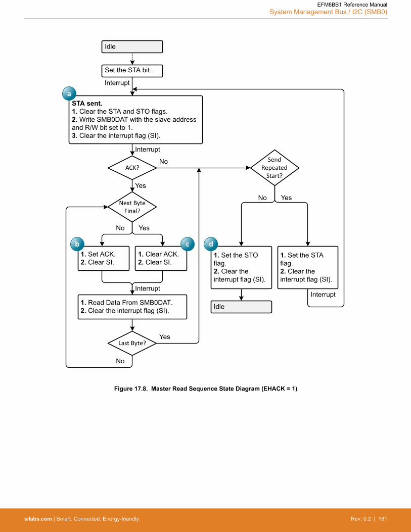
STA sent.1. Clear the STA and STO flags.2. Write SMB0DAT with the slave address and R/W bit set to 1.3. Clear the interrupt flag (SI).
aInterrupt
ACK?
Interrupt
Yes
No
Last Byte?
1. Read Data From SMB0DAT.2. Clear the interrupt flag (SI).
SendRepeated
Start?
Yes
1. Set the STO flag.2. Clear the interrupt flag (SI).
No
1. Set the STA flag.2. Clear the interrupt flag (SI).
Idle
Interrupt
1. Clear ACK.2. Clear SI.
Next Byte Final?
1. Set ACK.2. Clear SI.
YesNo
Interrupt
No
Yes
Set the STA bit.
Idle
b c d
Figure 17.8. Master Read Sequence State Diagram (EHACK = 1)
EFM8BB1 Reference ManualSystem Management Bus / I2C (SMB0)
silabs.com | Smart. Connected. Energy-friendly. Rev. 0.2 | 181

Slave Write Sequence
During a write sequence, an SMBus master writes data to a slave device. The slave in this transfer will be a receiver during the addressbyte, and a receiver during all data bytes. When slave events are enabled (INH = 0), the interface enters Slave Receiver Mode when aSTART followed by a slave address and direction bit (WRITE in this case) is received. If hardware ACK generation is disabled, uponentering Slave Receiver Mode, an interrupt is generated and the ACKRQ bit is set. The software must respond to the received slaveaddress with an ACK, or ignore the received slave address with a NACK. If hardware ACK generation is enabled, the hardware willapply the ACK for a slave address which matches the criteria set up by SMB0ADR and SMB0ADM. The interrupt will occur after theACK cycle.
If the received slave address is ignored (by software or hardware), slave interrupts will be inhibited until the next START is detected. Ifthe received slave address is acknowledged, zero or more data bytes are received.
If hardware ACK generation is disabled, the ACKRQ is set to 1 and an interrupt is generated after each received byte. Software mustwrite the ACK bit at that time to ACK or NACK the received byte.
With hardware ACK generation enabled, the SMBus hardware will automatically generate the ACK/NACK, and then post the interrupt. Itis important to note that the appropriate ACK or NACK value should be set up by the software prior to receiving the byte when hardwareACK generation is enabled.
The interface exits Slave Receiver Mode after receiving a STOP. The interface will switch to Slave Transmitter Mode if SMB0DAT iswritten while an active Slave Receiver. Figure 17.9 Typical Slave Write Sequence on page 182 shows a typical slave write sequenceas it appears on the bus. The corresponding firmware state diagram (combined with the slave read sequence) is shown in Figure17.10 Slave State Diagram (EHACK = 1) on page 183. Two received data bytes are shown, though any number of bytes may be re-ceived. Notice that the "data byte transferred" interrupts occur at different places in the sequence, depending on whether hardwareACK generation is enabled. The interrupt occurs before the ACK with hardware ACK generation disabled, and after the ACK whenhardware ACK generation is enabled.
e
PWSLAS Data ByteData Byte A AA
S = STARTP = STOPA = ACKW = WRITESLA = Slave Address
Received by SMBus Interface
Transmitted by SMBus Interface
Interrupts with Hardware ACK Disabled (EHACK = 0)
Interrupts with Hardware ACK Enabled (EHACK = 1)
f g he
f g h
Figure 17.9. Typical Slave Write Sequence
EFM8BB1 Reference ManualSystem Management Bus / I2C (SMB0)
silabs.com | Smart. Connected. Energy-friendly. Rev. 0.2 | 182
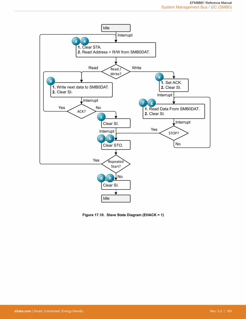
Interrupt
Idle
1. Clear STA.2. Read Address + R/W from SMB0DAT.
Read / Write?
Read Write
1. Write next data to SMB0DAT.2. Clear SI.
Interrupt
ACK?Yes No
Clear SI.
Interrupt
Clear STO.
Repeated Start?
Yes
Idle
No
1. Set ACK.2. Clear SI.
Clear SI.
1. Read Data From SMB0DAT.2. Clear SI.
Interrupt
STOP?
No
Interrupt
Yes
a e
b
d
f g
c
h
e
d h
Figure 17.10. Slave State Diagram (EHACK = 1)
EFM8BB1 Reference ManualSystem Management Bus / I2C (SMB0)
silabs.com | Smart. Connected. Energy-friendly. Rev. 0.2 | 183

Slave Read Sequence
During a read sequence, an SMBus master reads data from a slave device. The slave in this transfer will be a receiver during the ad-dress byte, and a transmitter during all data bytes. When slave events are enabled (INH = 0), the interface enters Slave Receiver Mode(to receive the slave address) when a START followed by a slave address and direction bit (READ in this case) is received. If hardwareACK generation is disabled, upon entering Slave Receiver Mode, an interrupt is generated and the ACKRQ bit is set. The softwaremust respond to the received slave address with an ACK, or ignore the received slave address with a NACK. If hardware ACK genera-tion is enabled, the hardware will apply the ACK for a slave address which matches the criteria set up by SMB0ADR and SMB0ADM.The interrupt will occur after the ACK cycle.
If the received slave address is ignored (by software or hardware), slave interrupts will be inhibited until the next START is detected. Ifthe received slave address is acknowledged, zero or more data bytes are transmitted. If the received slave address is acknowledged,data should be written to SMB0DAT to be transmitted. The interface enters slave transmitter mode, and transmits one or more bytes ofdata. After each byte is transmitted, the master sends an acknowledge bit; if the acknowledge bit is an ACK, SMB0DAT should be writ-ten with the next data byte. If the acknowledge bit is a NACK, SMB0DAT should not be written to before SI is cleared (an error conditionmay be generated if SMB0DAT is written following a received NACK while in slave transmitter mode). The interface exits slave trans-mitter mode after receiving a STOP. The interface will switch to slave receiver mode if SMB0DAT is not written following a Slave Trans-mitter interrupt. Figure 17.11 Typical Slave Read Sequence on page 184 shows a typical slave read sequence as it appears on thebus. The corresponding firmware state diagram (combined with the slave read sequence) is shown in Figure 17.10 Slave State Dia-gram (EHACK = 1) on page 183. Two transmitted data bytes are shown, though any number of bytes may be transmitted. Notice thatall of the “data byte transferred” interrupts occur after the ACK cycle in this mode, regardless of whether hardware ACK generation isenabled.
a
PRSLAS Data ByteData Byte A NA
S = STARTP = STOPN = NACKR = READSLA = Slave Address
Received by SMBus Interface
Transmitted by SMBus Interface
Interrupts with Hardware ACK Disabled (EHACK = 0)
Interrupts with Hardware ACK Enabled (EHACK = 1)
a b c d
b c d
Figure 17.11. Typical Slave Read Sequence
EFM8BB1 Reference ManualSystem Management Bus / I2C (SMB0)
silabs.com | Smart. Connected. Energy-friendly. Rev. 0.2 | 184
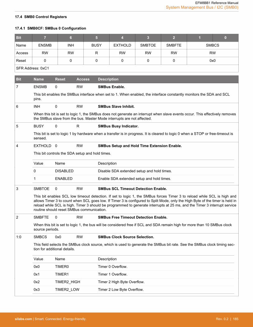
17.4 SMB0 Control Registers
17.4.1 SMB0CF: SMBus 0 Configuration
Bit 7 6 5 4 3 2 1 0
Name ENSMB INH BUSY EXTHOLD SMBTOE SMBFTE SMBCS
Access RW RW R RW RW RW RW
Reset 0 0 0 0 0 0 0x0
SFR Address: 0xC1
Bit Name Reset Access Description
7 ENSMB 0 RW SMBus Enable.
This bit enables the SMBus interface when set to 1. When enabled, the interface constantly monitors the SDA and SCLpins.
6 INH 0 RW SMBus Slave Inhibit.
When this bit is set to logic 1, the SMBus does not generate an interrupt when slave events occur. This effectively removesthe SMBus slave from the bus. Master Mode interrupts are not affected.
5 BUSY 0 R SMBus Busy Indicator.
This bit is set to logic 1 by hardware when a transfer is in progress. It is cleared to logic 0 when a STOP or free-timeout issensed.
4 EXTHOLD 0 RW SMBus Setup and Hold Time Extension Enable.
This bit controls the SDA setup and hold times.
Value Name Description
0 DISABLED Disable SDA extended setup and hold times.
1 ENABLED Enable SDA extended setup and hold times.
3 SMBTOE 0 RW SMBus SCL Timeout Detection Enable.
This bit enables SCL low timeout detection. If set to logic 1, the SMBus forces Timer 3 to reload while SCL is high andallows Timer 3 to count when SCL goes low. If Timer 3 is configured to Split Mode, only the High Byte of the timer is held inreload while SCL is high. Timer 3 should be programmed to generate interrupts at 25 ms, and the Timer 3 interrupt serviceroutine should reset SMBus communication.
2 SMBFTE 0 RW SMBus Free Timeout Detection Enable.
When this bit is set to logic 1, the bus will be considered free if SCL and SDA remain high for more than 10 SMBus clocksource periods.
1:0 SMBCS 0x0 RW SMBus Clock Source Selection.
This field selects the SMBus clock source, which is used to generate the SMBus bit rate. See the SMBus clock timing sec-tion for additional details.
Value Name Description
0x0 TIMER0 Timer 0 Overflow.
0x1 TIMER1 Timer 1 Overflow.
0x2 TIMER2_HIGH Timer 2 High Byte Overflow.
0x3 TIMER2_LOW Timer 2 Low Byte Overflow.
EFM8BB1 Reference ManualSystem Management Bus / I2C (SMB0)
silabs.com | Smart. Connected. Energy-friendly. Rev. 0.2 | 185
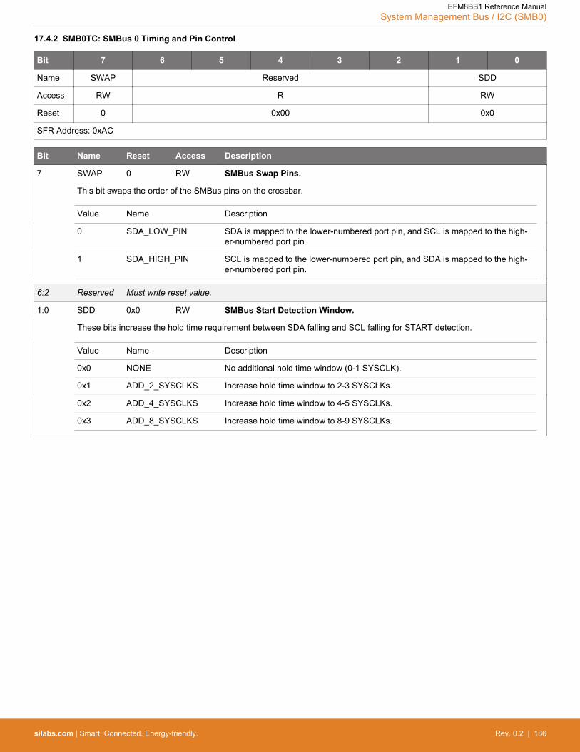
17.4.2 SMB0TC: SMBus 0 Timing and Pin Control
Bit 7 6 5 4 3 2 1 0
Name SWAP Reserved SDD
Access RW R RW
Reset 0 0x00 0x0
SFR Address: 0xAC
Bit Name Reset Access Description
7 SWAP 0 RW SMBus Swap Pins.
This bit swaps the order of the SMBus pins on the crossbar.
Value Name Description
0 SDA_LOW_PIN SDA is mapped to the lower-numbered port pin, and SCL is mapped to the high-er-numbered port pin.
1 SDA_HIGH_PIN SCL is mapped to the lower-numbered port pin, and SDA is mapped to the high-er-numbered port pin.
6:2 Reserved Must write reset value.
1:0 SDD 0x0 RW SMBus Start Detection Window.
These bits increase the hold time requirement between SDA falling and SCL falling for START detection.
Value Name Description
0x0 NONE No additional hold time window (0-1 SYSCLK).
0x1 ADD_2_SYSCLKS Increase hold time window to 2-3 SYSCLKs.
0x2 ADD_4_SYSCLKS Increase hold time window to 4-5 SYSCLKs.
0x3 ADD_8_SYSCLKS Increase hold time window to 8-9 SYSCLKs.
EFM8BB1 Reference ManualSystem Management Bus / I2C (SMB0)
silabs.com | Smart. Connected. Energy-friendly. Rev. 0.2 | 186

17.4.3 SMB0CN0: SMBus 0 Control
Bit 7 6 5 4 3 2 1 0
Name MASTER TXMODE STA STO ACKRQ ARBLOST ACK SI
Access R R RW RW R R RW RW
Reset 0 0 0 0 0 0 0 0
SFR Address: 0xC0 (bit-addressable)
Bit Name Reset Access Description
7 MASTER 0 R SMBus Master/Slave Indicator.
This read-only bit indicates when the SMBus is operating as a master.
Value Name Description
0 SLAVE SMBus operating in slave mode.
1 MASTER SMBus operating in master mode.
6 TXMODE 0 R SMBus Transmit Mode Indicator.
This read-only bit indicates when the SMBus is operating as a transmitter.
Value Name Description
0 RECEIVER SMBus in Receiver Mode.
1 TRANSMITTER SMBus in Transmitter Mode.
5 STA 0 RW SMBus Start Flag.
When reading STA, a '1' indicates that a start or repeated start condition was detected on the bus.
Writing a '1' to the STA bit initiates a start or repeated start on the bus.
4 STO 0 RW SMBus Stop Flag.
When reading STO, a '1' indicates that a stop condition was detected on the bus (in slave mode) or is pending (in mastermode).
When acting as a master, writing a '1' to the STO bit initiates a stop condition on the bus. This bit is cleared by hardware.
3 ACKRQ 0 R SMBus Acknowledge Request.
Value Name Description
0 NOT_SET No ACK requested.
1 REQUESTED ACK requested.
2 ARBLOST 0 R SMBus Arbitration Lost Indicator.
Value Name Description
0 NOT_SET No arbitration error.
1 ERROR Arbitration error occurred.
1 ACK 0 RW SMBus Acknowledge.
When read as a master, the ACK bit indicates whether an ACK (1) or NACK (0) is received during the most recent bytetransfer.
As a slave, this bit should be written to send an ACK (1) or NACK (0) to a master request. Note that the logic level of theACK bit on the SMBus interface is inverted from the logic of the register ACK bit.
EFM8BB1 Reference ManualSystem Management Bus / I2C (SMB0)
silabs.com | Smart. Connected. Energy-friendly. Rev. 0.2 | 187

Bit Name Reset Access Description
0 SI 0 RW SMBus Interrupt Flag.
This bit is set by hardware to indicate that the current SMBus state machine operation (such as writing a data or addressbyte) is complete, and the hardware needs additional control from the firmware to proceed. While SI is set, SCL is held lowand SMBus is stalled. SI must be cleared by firmware. Clearing SI initiates the next SMBus state machine operation.
17.4.4 SMB0ADR: SMBus 0 Slave Address
Bit 7 6 5 4 3 2 1 0
Name SLV GC
Access RW RW
Reset 0x00 0
SFR Address: 0xD7
Bit Name Reset Access Description
7:1 SLV 0x00 RW SMBus Hardware Slave Address.
Defines the SMBus Slave Address(es) for automatic hardware acknowledgement. Only address bits which have a 1 in thecorresponding bit position in SLVM are checked against the incoming address. This allows multiple addresses to be recog-nized.
0 GC 0 RW General Call Address Enable.
When hardware address recognition is enabled (EHACK = 1), this bit will determine whether the General Call Address(0x00) is also recognized by hardware.
Value Name Description
0 IGNORED General Call Address is ignored.
1 RECOGNIZED General Call Address is recognized.
EFM8BB1 Reference ManualSystem Management Bus / I2C (SMB0)
silabs.com | Smart. Connected. Energy-friendly. Rev. 0.2 | 188

17.4.5 SMB0ADM: SMBus 0 Slave Address Mask
Bit 7 6 5 4 3 2 1 0
Name SLVM EHACK
Access RW RW
Reset 0x7F 0
SFR Address: 0xD6
Bit Name Reset Access Description
7:1 SLVM 0x7F RW SMBus Slave Address Mask.
Defines which bits of register SMB0ADR are compared with an incoming address byte, and which bits are ignored. Any bitset to 1 in SLVM enables comparisons with the corresponding bit in SLV. Bits set to 0 are ignored (can be either 0 or 1 inthe incoming address).
0 EHACK 0 RW Hardware Acknowledge Enable.
Enables hardware acknowledgement of slave address and received data bytes.
Value Name Description
0 ADR_ACK_MANUAL Firmware must manually acknowledge all incoming address and data bytes.
1 ADR_ACK_AUTOMAT-IC
Automatic slave address recognition and hardware acknowledge is enabled.
17.4.6 SMB0DAT: SMBus 0 Data
Bit 7 6 5 4 3 2 1 0
Name SMB0DAT
Access RW
Reset 0x00
SFR Address: 0xC2
Bit Name Reset Access Description
7:0 SMB0DAT 0x00 RW SMBus 0 Data.
The SMB0DAT register contains a byte of data to be transmitted on the SMBus serial interface or a byte that has just beenreceived on the SMBus serial interface. The CPU can safely read from or write to this register whenever the SI serial inter-rupt flag is set to logic 1. The serial data in the register remains stable as long as the SI flag is set. When the SI flag is notset, the system may be in the process of shifting data in/out and the CPU should not attempt to access this register.
EFM8BB1 Reference ManualSystem Management Bus / I2C (SMB0)
silabs.com | Smart. Connected. Energy-friendly. Rev. 0.2 | 189

18. Timers (Timer0, Timer1, Timer2, and Timer3)
18.1 Introduction
Four counter/timers ar included in the device: two are 16-bit counter/timers compatible with those found in the standard 8051, and twoare 16-bit auto-reload timers for timing peripherals or for general purpose use. These timers can be used to measure time intervals,count external events and generate periodic interrupt requests. Timer 0 and Timer 1 are nearly identical and have four primary modesof operation. Timer 2 and Timer 3 are also identical and offer both 16-bit and split 8-bit timer functionality with auto-reload capabilities.Timer 2 and Timer 3 both offer a capture function, but are different in their system-level connections. Timer 2 is capable of performing acapture function on an external signal input routed through the crossbar, while the Timer 3 capture is dedicated to the low-frequencyoscillator output.
Timers 0 and 1 may be clocked by one of five sources, determined by the Timer Mode Select bits (T1M–T0M) and the Clock Scale bits(SCA1–SCA0). The Clock Scale bits define a pre-scaled clock from which Timer 0 and/or Timer 1 may be clocked.
Timer 0/1 may then be configured to use this pre-scaled clock signal or the system clock. Timer 2 and Timer 3 may be clocked by thesystem clock, the system clock divided by 12, or the external clock divided by 8.
Timer 0 and Timer 1 may also be operated as counters. When functioning as a counter, a counter/timer register is incremented on eachhigh-to-low transition at the selected input pin (T0 or T1). Events with a frequency of up to one-fourth the system clock frequency canbe counted. The input signal need not be periodic, but it must be held at a given level for at least two full system clock cycles to ensurethe level is properly sampled.
Table 18.1. Timer Modes
Timer 0 and Timer 1 Modes Timer 2 Modes Timer 3 Modes
13-bit counter/timer 16-bit timer with auto-reload 16-bit timer with auto-reload
16-bit counter/timer Two 8-bit timers with auto-reload Two 8-bit timers with auto-reload
8-bit counter/timer with auto-reload Input pin capture Low-frequency oscillator capture
Two 8-bit counter/timers (Timer 0 only)
18.2 Features
Timer 0 and Timer 1 include the following features:• Standard 8051 timers, supporting backwards-compatibility with firmware and hardware.• Clock sources include SYSCLK, SYSCLK divided by 12, 4, or 48, the External Clock divided by 8, or an external pin.• 8-bit auto-reload counter/timer mode• 13-bit counter/timer mode• 16-bit counter/timer mode• Dual 8-bit counter/timer mode (Timer 0)
Timer 2 and Timer 3 are 16-bit timers including the following features:• Clock sources include SYSCLK, SYSCLK divided by 12, or the External Clock divided by 8.• 16-bit auto-reload timer mode• Dual 8-bit auto-reload timer mode• External pin capture (Timer 2)• LFOSC0 capture (Timer 3)
EFM8BB1 Reference ManualTimers (Timer0, Timer1, Timer2, and Timer3)
silabs.com | Smart. Connected. Energy-friendly. Rev. 0.2 | 190

18.3 Functional Description
18.3.1 System Connections
All four timers are capable of clocking other peripherals and triggering events in the system. The individual peripherals select whichtimer to use for their respective functions. Note that the Timer 2 and Timer 3 high overflows apply to the full timer when operating in 16-bit mode or the high-byte timer when operating in 8-bit split mode.
Table 18.2. Timer Peripheral Clocking / Event Triggering
Function T0 Overflow T1 Overflow T2 High Over-flow
T2 Low Over-flow
T3 High Over-flow
T3 Low Over-flow
UART0 Baud Rate Yes
SMBus 0 Clock Rate (Master) Yes Yes Yes Yes
SMBus 0 SCL Low Timeout Yes
PCA0 Clock Yes
ADC0 Conversion Start Yes Yes1 Yes1 Yes1 Yes1
Notes:1. The high-side overflow is used when the timer is in 16-bit mode. The low-side overflow is used in 8-bit mode.
18.3.2 Timer 0 and Timer 1
Timer 0 and Timer 1 are each implemented as a 16-bit register accessed as two separate bytes: a low byte (TL0 or TL1) and a highbyte (TH0 or TH1). The Counter/Timer Control register (TCON) is used to enable Timer 0 and Timer 1 as well as indicate status. Timer0 interrupts can be enabled by setting the ET0 bit in the IE register. Timer 1 interrupts can be enabled by setting the ET1 bit in the IEregister. Both counter/timers operate in one of four primary modes selected by setting the Mode Select bits T1M1–T0M0 in the Counter/Timer Mode register (TMOD). Each timer can be configured independently for the supported operating modes.
EFM8BB1 Reference ManualTimers (Timer0, Timer1, Timer2, and Timer3)
silabs.com | Smart. Connected. Energy-friendly. Rev. 0.2 | 191

18.3.2.1 Operational Modes
Mode 0: 13-bit Counter/Timer
Timer 0 and Timer 1 operate as 13-bit counter/timers in Mode 0. The following describes the configuration and operation of Timer 0.However, both timers operate identically, and Timer 1 is configured in the same manner as described for Timer 0.
The TH0 register holds the eight MSBs of the 13-bit counter/timer. TL0 holds the five LSBs in bit positions TL0.4–TL0.0. The threeupper bits of TL0 (TL0.7–TL0.5) are indeterminate and should be masked out or ignored when reading. As the 13-bit timer registerincrements and overflows from 0x1FFF (all ones) to 0x0000, the timer overflow flag TF0 in TCON is set and an interrupt occurs if Timer0 interrupts are enabled. The overflow rate for Timer 0 in 13-bit mode is:
FTIMER0 =FInput Clock
213 – TH0:TL0=
FInput Clock8192 – TH0:TL0
The CT0 bit in the TMOD register selects the counter/timer's clock source. When CT0 is set to logic 1, high-to-low transitions at theselected Timer 0 input pin (T0) increment the timer register. Events with a frequency of up to one-fourth the system clock frequency canbe counted. The input signal need not be periodic, but it must be held at a given level for at least two full system clock cycles to ensurethe level is properly sampled. Clearing CT selects the clock defined by the T0M bit in register CKCON0. When T0M is set, Timer 0 isclocked by the system clock. When T0M is cleared, Timer 0 is clocked by the source selected by the Clock Scale bits in CKCON0.
Setting the TR0 bit enables the timer when either GATE0 in the TMOD register is logic 0 or based on the input signal INT0. The IN0PLbit setting in IT01CF changes which state of INT0 input starts the timer counting. Setting GATE0 to 1 allows the timer to be controlledby the external input signal INT0, facilitating pulse width measurements.
Table 18.3. Timer 0 Run Control Options
TR0 GATE0 INT0 IN0PL Counter/Timer
0 X X X Disabled
1 0 X X Enabled
1 1 0 0 Disabled
1 1 0 1 Enabled
1 1 1 0 Enabled
1 1 1 1 Disabled
Note:1. X = Don't Care
Setting TR0 does not force the timer to reset. The timer registers should be loaded with the desired initial value before the timer isenabled.
TL1 and TH1 form the 13-bit register for Timer 1 in the same manner as described above for TL0 and TH0. Timer 1 is configured andcontrolled using the relevant TCON and TMOD bits just as with Timer 0. The input signal INT1 is used with Timer 1, and IN1PL inregister IT01CF determines the INT1 state that starts Timer 1 counting.
EFM8BB1 Reference ManualTimers (Timer0, Timer1, Timer2, and Timer3)
silabs.com | Smart. Connected. Energy-friendly. Rev. 0.2 | 192

TCLKTR0
0
1
0
1SYSCLK
Pre-scaled Clock
GATE0
IN0PL XOR
T0M
T0
INT0
CT0
TL0(5 bits)
TH0(8 bits) TF0
(Interrupt Flag)
Figure 18.1. T0 Mode 0 Block Diagram
Mode 1: 16-bit Counter/Timer
Mode 1 operation is the same as Mode 0, except that the counter/timer registers use all 16 bits. The counter/timers are enabled andconfigured in Mode 1 in the same manner as for Mode 0. The overflow rate for Timer 0 in 16-bit mode is:
FTIMER0 =FInput Clock
216 – TH0:TL0=
FInput Clock65536 – TH0:TL0
EFM8BB1 Reference ManualTimers (Timer0, Timer1, Timer2, and Timer3)
silabs.com | Smart. Connected. Energy-friendly. Rev. 0.2 | 193

Mode 2: 8-bit Counter/Timer with Auto-Reload
Mode 2 configures Timer 0 and Timer 1 to operate as 8-bit counter/timers with automatic reload of the start value. TL0 holds the countand TH0 holds the reload value. When the counter in TL0 overflows from all ones to 0x00, the timer overflow flag TF0 in the TCONregister is set and the counter in TL0 is reloaded from TH0. If Timer 0 interrupts are enabled, an interrupt will occur when the TF0 flag isset. The reload value in TH0 is not changed. TL0 must be initialized to the desired value before enabling the timer for the first count tobe correct. When in Mode 2, Timer 1 operates identically to Timer 0.
The overflow rate for Timer 0 in 8-bit auto-reload mode is:
FTIMER0 =FInput Clock
28 – TH0=
FInput Clock256 – TH0
Both counter/timers are enabled and configured in Mode 2 in the same manner as Mode 0. Setting the TR0 bit enables the timer wheneither GATE0 in the TMOD register is logic 0 or when the input signal INT0 is active as defined by bit IN0PL in register IT01CF.
Reload
TL0(8 bits)
TH0(8 bits)
TF0(Interrupt Flag)
TCLKTR0
0
1
0
1SYSCLK
Pre-scaled Clock
GATE0
IN0PL XOR
T0M
T0
INT0
CT0
Figure 18.2. T0 Mode 2 Block Diagram
EFM8BB1 Reference ManualTimers (Timer0, Timer1, Timer2, and Timer3)
silabs.com | Smart. Connected. Energy-friendly. Rev. 0.2 | 194
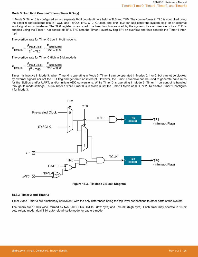
Mode 3: Two 8-bit Counter/Timers (Timer 0 Only)
In Mode 3, Timer 0 is configured as two separate 8-bit counter/timers held in TL0 and TH0. The counter/timer in TL0 is controlled usingthe Timer 0 control/status bits in TCON and TMOD: TR0, CT0, GATE0, and TF0. TL0 can use either the system clock or an externalinput signal as its timebase. The TH0 register is restricted to a timer function sourced by the system clock or prescaled clock. TH0 isenabled using the Timer 1 run control bit TR1. TH0 sets the Timer 1 overflow flag TF1 on overflow and thus controls the Timer 1 inter-rupt.
The overflow rate for Timer 0 Low in 8-bit mode is:
FTIMER0 =FInput Clock
28 – TL0=
FInput Clock256 – TL0
The overflow rate for Timer 0 High in 8-bit mode is:
FTIMER0 =FInput Clock
28 – TH0=
FInput Clock256 – TH0
Timer 1 is inactive in Mode 3. When Timer 0 is operating in Mode 3, Timer 1 can be operated in Modes 0, 1 or 2, but cannot be clockedby external signals nor set the TF1 flag and generate an interrupt. However, the Timer 1 overflow can be used to generate baud ratesfor the SMBus and/or UART, and/or initiate ADC conversions. While Timer 0 is operating in Mode 3, Timer 1 run control is handledthrough its mode settings. To run Timer 1 while Timer 0 is in Mode 3, set the Timer 1 Mode as 0, 1, or 2. To disable Timer 1, configureit for Mode 3.
TCLKTR0
0
1
0
1SYSCLK
Pre-scaled Clock
GATE0
IN0PL XOR
T0M
T0
INT0
CT0
TR1
TL0(8 bits) TF0
(Interrupt Flag)
TH0(8 bits) TF1
(Interrupt Flag)
Figure 18.3. T0 Mode 3 Block Diagram
18.3.3 Timer 2 and Timer 3
Timer 2 and Timer 3 are functionally equivalent, with the only differences being the top-level connections to other parts of the system.
The timers are 16 bits wide, formed by two 8-bit SFRs: TMRnL (low byte) and TMRnH (high byte). Each timer may operate in 16-bitauto-reload mode, dual 8-bit auto-reload (split) mode, or capture mode.
EFM8BB1 Reference ManualTimers (Timer0, Timer1, Timer2, and Timer3)
silabs.com | Smart. Connected. Energy-friendly. Rev. 0.2 | 195

Clock Selection
Clocking for each timer is configured using the TnXCLK bit field and the TnML and TnMH bits. Both timers may be clocked by the sys-tem clock, the system clock divided by 12, or the external clock source divided by 8 (synchronized with SYSCLK).
FSYSCLK > FEXTCLK × 67
When operating in one of the 16-bit modes, the low-side timer clock is used to clock the entire 16-bit timer.
To Timer Low Clock Input
Timer Clock Selection
SYSCLK
TnXCLK
TnML
TnMH
To Timer High Clock Input
(for split mode)
External Clock / 8
SYSCLK / 12
Figure 18.4. Timer 2 and 3 Clock Source Selection
EFM8BB1 Reference ManualTimers (Timer0, Timer1, Timer2, and Timer3)
silabs.com | Smart. Connected. Energy-friendly. Rev. 0.2 | 196

Capture Sources
Capture mode allows an external input (Timer 2) or the low-frequency oscillator clock (Timer 3) to be measured against the selectedclock source. The timer 2 capture input (T2) is routed to an external pin using the crossbar.
Capture Sources
T2 Pin
LFOSC0
To Timer 2 Capture Input
To Timer 3 Capture Input
Figure 18.5. Timer 2 and 3 Capture Sources
18.3.3.1 16-bit Timer with Auto-Reload
When TnSPLIT is zero, the timer operates as a 16-bit timer with auto-reload. In this mode, the selected clock source increments thetimer on every clock. As the 16-bit timer register increments and overflows from 0xFFFF to 0x0000, the 16-bit value in the timer reloadregisters (TMRnRLH and TMRnRLL) is loaded into the main timer count register, and the High Byte Overflow Flag (TFnH) is set. If thetimer interrupts are enabled, an interrupt is generated on each timer overflow. Additionally, if the timer interrupts are enabled and theTFnLEN bit is set, an interrupt is generated each time the lower 8 bits (TMRnL) overflow from 0xFF to 0x00.
The overflow rate of the timer in split 16-bit auto-reload mode is:
FTIMERn =FInput Clock
216 – TMRnRLH:TMRnRLL=
FInput Clock65536 – TMRnRLH:TMRnRLL
TMRnL TMRnH
Reload
Interrupt
TFnL Overflow
TFnH Overflow
TMRnRLL TMRnRLH
TFnLEN
TRnTimer Low Clock
Figure 18.6. 16-Bit Mode Block Diagram
EFM8BB1 Reference ManualTimers (Timer0, Timer1, Timer2, and Timer3)
silabs.com | Smart. Connected. Energy-friendly. Rev. 0.2 | 197

18.3.3.2 8-bit Timers with Auto-Reload (Split Mode)
When TnSPLIT is set, the timer operates as two 8-bit timers (TMRnH and TMRnL). Both 8-bit timers operate in auto-reload mode.TMRnRLL holds the reload value for TMRnL; TMRnRLH holds the reload value for TMRnH. The TRn bit in TMRnCN handles the runcontrol for TMRnH. TMRnL is always running when configured for 8-bit auto-reload mode. As shown in the clock source selection tree,the two halves of the timer may be clocked from SYSCLK or by the source selected by the TnXCLK bits.
The overflow rate of the low timer in split 8-bit auto-reload mode is:
FTIMERn Low =FInput Clock
28 – TMRnRLL=
FInput Clock256 – TMRnRLL
The overflow rate of the high timer in split 8-bit auto-reload mode is:
FTIMERn High =FInput Clock
28 – TMRnRLH=
FInput Clock256 – TMRnRLH
The TFnH bit is set when TMRnH overflows from 0xFF to 0x00; the TFnL bit is set when TMRnL overflows from 0xFF to 0x00. Whentimer interrupts are enabled, an interrupt is generated each time TMRnH overflows. If timer interrupts are enabled and TFnLEN is set,an interrupt is generated each time either TMRnL or TMRnH overflows. When TFnLEN is enabled, software must check the TFnH andTFnL flags to determine the source of the timer interrupt. The TFnH and TFnL interrupt flags are not cleared by hardware and must bemanually cleared by software.
TMRnH
TMRnRLHReload
Reload
TCLK
TMRnRLL
Interrupt
TFnL Overflow
TFnLEN
TMRnL
TFnH OverflowTRn
Timer High Clock
Timer Low Clock
Figure 18.7. 8-Bit Split Mode Block Diagram
EFM8BB1 Reference ManualTimers (Timer0, Timer1, Timer2, and Timer3)
silabs.com | Smart. Connected. Energy-friendly. Rev. 0.2 | 198

18.3.3.3 Capture Mode
Capture mode allows a system event to be measured against the selected clock source. When used in capture mode, the timer clocksnormally from the selected clock source through the entire range of 16-bit values from 0x0000 to 0xFFFF.
Setting TFnCEN to 1 enables capture mode. In this mode, TnSPLIT should be set to 0, as the full 16-bit timer is used. Upon a fallingedge of the input capture signal, the contents of the timer register (TMRnH:TMRnL) are loaded into the reload registers(TMRnRLH:TMRnRLL) and the TFnH flag is set. By recording the difference between two successive timer capture values, the periodof the captured signal can be determined with respect to the selected timer clock.
TMRnL TMRnHTRn
TMRnRLL TMRnRLH
CaptureTFnCEN
TFnH (Interrupt)
Capture Source
Timer Low Clock
Figure 18.8. Capture Mode Block Diagram
EFM8BB1 Reference ManualTimers (Timer0, Timer1, Timer2, and Timer3)
silabs.com | Smart. Connected. Energy-friendly. Rev. 0.2 | 199

18.4 Timer 0, 1, 2 and 3, Control Registers
18.4.1 CKCON0: Clock Control 0
Bit 7 6 5 4 3 2 1 0
Name T3MH T3ML T2MH T2ML T1M T0M SCA
Access RW RW RW RW RW RW RW
Reset 0 0 0 0 0 0 0x0
SFR Address: 0x8E
Bit Name Reset Access Description
7 T3MH 0 RW Timer 3 High Byte Clock Select.
Selects the clock supplied to the Timer 3 high byte (split 8-bit timer mode only).
Value Name Description
0 EXTERNAL_CLOCK Timer 3 high byte uses the clock defined by T3XCLK in TMR3CN0.
1 SYSCLK Timer 3 high byte uses the system clock.
6 T3ML 0 RW Timer 3 Low Byte Clock Select.
Selects the clock supplied to Timer 3. Selects the clock supplied to the lower 8-bit timer in split 8-bit timer mode.
Value Name Description
0 EXTERNAL_CLOCK Timer 3 low byte uses the clock defined by T3XCLK in TMR3CN0.
1 SYSCLK Timer 3 low byte uses the system clock.
5 T2MH 0 RW Timer 2 High Byte Clock Select.
Selects the clock supplied to the Timer 2 high byte (split 8-bit timer mode only).
Value Name Description
0 EXTERNAL_CLOCK Timer 2 high byte uses the clock defined by T2XCLK in TMR2CN0.
1 SYSCLK Timer 2 high byte uses the system clock.
4 T2ML 0 RW Timer 2 Low Byte Clock Select.
Selects the clock supplied to Timer 2. If Timer 2 is configured in split 8-bit timer mode, this bit selects the clock supplied tothe lower 8-bit timer.
Value Name Description
0 EXTERNAL_CLOCK Timer 2 low byte uses the clock defined by T2XCLK in TMR2CN0.
1 SYSCLK Timer 2 low byte uses the system clock.
3 T1M 0 RW Timer 1 Clock Select.
Selects the clock source supplied to Timer 1. Ignored when C/T1 is set to 1.
Value Name Description
0 PRESCALE Timer 1 uses the clock defined by the prescale field, SCA.
1 SYSCLK Timer 1 uses the system clock.
EFM8BB1 Reference ManualTimers (Timer0, Timer1, Timer2, and Timer3)
silabs.com | Smart. Connected. Energy-friendly. Rev. 0.2 | 200

Bit Name Reset Access Description
2 T0M 0 RW Timer 0 Clock Select.
Selects the clock source supplied to Timer 0. Ignored when C/T0 is set to 1.
Value Name Description
0 PRESCALE Counter/Timer 0 uses the clock defined by the prescale field, SCA.
1 SYSCLK Counter/Timer 0 uses the system clock.
1:0 SCA 0x0 RW Timer 0/1 Prescale.
These bits control the Timer 0/1 Clock Prescaler:
Value Name Description
0x0 SYSCLK_DIV_12 System clock divided by 12.
0x1 SYSCLK_DIV_4 System clock divided by 4.
0x2 SYSCLK_DIV_48 System clock divided by 48.
0x3 EXTOSC_DIV_8 External oscillator divided by 8 (synchronized with the system clock).
EFM8BB1 Reference ManualTimers (Timer0, Timer1, Timer2, and Timer3)
silabs.com | Smart. Connected. Energy-friendly. Rev. 0.2 | 201
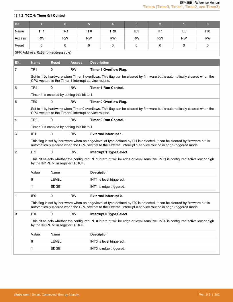
18.4.2 TCON: Timer 0/1 Control
Bit 7 6 5 4 3 2 1 0
Name TF1 TR1 TF0 TR0 IE1 IT1 IE0 IT0
Access RW RW RW RW RW RW RW RW
Reset 0 0 0 0 0 0 0 0
SFR Address: 0x88 (bit-addressable)
Bit Name Reset Access Description
7 TF1 0 RW Timer 1 Overflow Flag.
Set to 1 by hardware when Timer 1 overflows. This flag can be cleared by firmware but is automatically cleared when theCPU vectors to the Timer 1 interrupt service routine.
6 TR1 0 RW Timer 1 Run Control.
Timer 1 is enabled by setting this bit to 1.
5 TF0 0 RW Timer 0 Overflow Flag.
Set to 1 by hardware when Timer 0 overflows. This flag can be cleared by firmware but is automatically cleared when theCPU vectors to the Timer 0 interrupt service routine.
4 TR0 0 RW Timer 0 Run Control.
Timer 0 is enabled by setting this bit to 1.
3 IE1 0 RW External Interrupt 1.
This flag is set by hardware when an edge/level of type defined by IT1 is detected. It can be cleared by firmware but isautomatically cleared when the CPU vectors to the External Interrupt 1 service routine in edge-triggered mode.
2 IT1 0 RW Interrupt 1 Type Select.
This bit selects whether the configured INT1 interrupt will be edge or level sensitive. INT1 is configured active low or highby the IN1PL bit in register IT01CF.
Value Name Description
0 LEVEL INT1 is level triggered.
1 EDGE INT1 is edge triggered.
1 IE0 0 RW External Interrupt 0.
This flag is set by hardware when an edge/level of type defined by IT0 is detected. It can be cleared by firmware but isautomatically cleared when the CPU vectors to the External Interrupt 0 service routine in edge-triggered mode.
0 IT0 0 RW Interrupt 0 Type Select.
This bit selects whether the configured INT0 interrupt will be edge or level sensitive. INT0 is configured active low or highby the IN0PL bit in register IT01CF.
Value Name Description
0 LEVEL INT0 is level triggered.
1 EDGE INT0 is edge triggered.
EFM8BB1 Reference ManualTimers (Timer0, Timer1, Timer2, and Timer3)
silabs.com | Smart. Connected. Energy-friendly. Rev. 0.2 | 202

18.4.3 TMOD: Timer 0/1 Mode
Bit 7 6 5 4 3 2 1 0
Name GATE1 CT1 T1M GATE0 CT0 T0M
Access RW RW RW RW RW RW
Reset 0 0 0x0 0 0 0x0
SFR Address: 0x89
Bit Name Reset Access Description
7 GATE1 0 RW Timer 1 Gate Control.
Value Name Description
0 DISABLED Timer 1 enabled when TR1 = 1 irrespective of INT1 logic level.
1 ENABLED Timer 1 enabled only when TR1 = 1 and INT1 is active as defined by bit IN1PL inregister IT01CF.
6 CT1 0 RW Counter/Timer 1 Select.
Value Name Description
0 TIMER Timer Mode. Timer 1 increments on the clock defined by T1M in the CKCON0register.
1 COUNTER Counter Mode. Timer 1 increments on high-to-low transitions of an external pin(T1).
5:4 T1M 0x0 RW Timer 1 Mode Select.
These bits select the Timer 1 operation mode.
Value Name Description
0x0 MODE0 Mode 0, 13-bit Counter/Timer
0x1 MODE1 Mode 1, 16-bit Counter/Timer
0x2 MODE2 Mode 2, 8-bit Counter/Timer with Auto-Reload
0x3 MODE3 Mode 3, Timer 1 Inactive
3 GATE0 0 RW Timer 0 Gate Control.
Value Name Description
0 DISABLED Timer 0 enabled when TR0 = 1 irrespective of INT0 logic level.
1 ENABLED Timer 0 enabled only when TR0 = 1 and INT0 is active as defined by bit IN0PL inregister IT01CF.
2 CT0 0 RW Counter/Timer 0 Select.
Value Name Description
0 TIMER Timer Mode. Timer 0 increments on the clock defined by T0M in the CKCON0register.
1 COUNTER Counter Mode. Timer 0 increments on high-to-low transitions of an external pin(T0).
EFM8BB1 Reference ManualTimers (Timer0, Timer1, Timer2, and Timer3)
silabs.com | Smart. Connected. Energy-friendly. Rev. 0.2 | 203

Bit Name Reset Access Description
1:0 T0M 0x0 RW Timer 0 Mode Select.
These bits select the Timer 0 operation mode.
Value Name Description
0x0 MODE0 Mode 0, 13-bit Counter/Timer
0x1 MODE1 Mode 1, 16-bit Counter/Timer
0x2 MODE2 Mode 2, 8-bit Counter/Timer with Auto-Reload
0x3 MODE3 Mode 3, Two 8-bit Counter/Timers
18.4.4 TL0: Timer 0 Low Byte
Bit 7 6 5 4 3 2 1 0
Name TL0
Access RW
Reset 0x00
SFR Address: 0x8A
Bit Name Reset Access Description
7:0 TL0 0x00 RW Timer 0 Low Byte.
The TL0 register is the low byte of the 16-bit Timer 0.
18.4.5 TL1: Timer 1 Low Byte
Bit 7 6 5 4 3 2 1 0
Name TL1
Access RW
Reset 0x00
SFR Address: 0x8B
Bit Name Reset Access Description
7:0 TL1 0x00 RW Timer 1 Low Byte.
The TL1 register is the low byte of the 16-bit Timer 1.
EFM8BB1 Reference ManualTimers (Timer0, Timer1, Timer2, and Timer3)
silabs.com | Smart. Connected. Energy-friendly. Rev. 0.2 | 204

18.4.6 TH0: Timer 0 High Byte
Bit 7 6 5 4 3 2 1 0
Name TH0
Access RW
Reset 0x00
SFR Address: 0x8C
Bit Name Reset Access Description
7:0 TH0 0x00 RW Timer 0 High Byte.
The TH0 register is the high byte of the 16-bit Timer 0.
18.4.7 TH1: Timer 1 High Byte
Bit 7 6 5 4 3 2 1 0
Name TH1
Access RW
Reset 0x00
SFR Address: 0x8D
Bit Name Reset Access Description
7:0 TH1 0x00 RW Timer 1 High Byte.
The TH1 register is the high byte of the 16-bit Timer 1.
EFM8BB1 Reference ManualTimers (Timer0, Timer1, Timer2, and Timer3)
silabs.com | Smart. Connected. Energy-friendly. Rev. 0.2 | 205
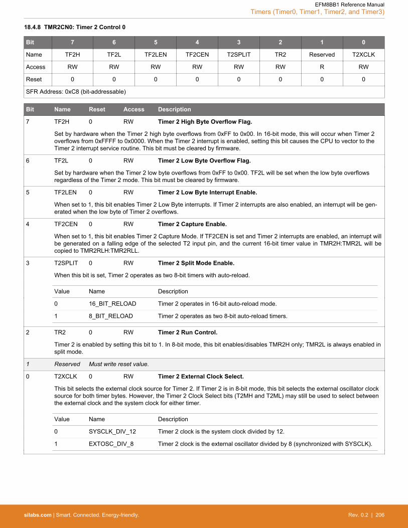
18.4.8 TMR2CN0: Timer 2 Control 0
Bit 7 6 5 4 3 2 1 0
Name TF2H TF2L TF2LEN TF2CEN T2SPLIT TR2 Reserved T2XCLK
Access RW RW RW RW RW RW R RW
Reset 0 0 0 0 0 0 0 0
SFR Address: 0xC8 (bit-addressable)
Bit Name Reset Access Description
7 TF2H 0 RW Timer 2 High Byte Overflow Flag.
Set by hardware when the Timer 2 high byte overflows from 0xFF to 0x00. In 16-bit mode, this will occur when Timer 2overflows from 0xFFFF to 0x0000. When the Timer 2 interrupt is enabled, setting this bit causes the CPU to vector to theTimer 2 interrupt service routine. This bit must be cleared by firmware.
6 TF2L 0 RW Timer 2 Low Byte Overflow Flag.
Set by hardware when the Timer 2 low byte overflows from 0xFF to 0x00. TF2L will be set when the low byte overflowsregardless of the Timer 2 mode. This bit must be cleared by firmware.
5 TF2LEN 0 RW Timer 2 Low Byte Interrupt Enable.
When set to 1, this bit enables Timer 2 Low Byte interrupts. If Timer 2 interrupts are also enabled, an interrupt will be gen-erated when the low byte of Timer 2 overflows.
4 TF2CEN 0 RW Timer 2 Capture Enable.
When set to 1, this bit enables Timer 2 Capture Mode. If TF2CEN is set and Timer 2 interrupts are enabled, an interrupt willbe generated on a falling edge of the selected T2 input pin, and the current 16-bit timer value in TMR2H:TMR2L will becopied to TMR2RLH:TMR2RLL.
3 T2SPLIT 0 RW Timer 2 Split Mode Enable.
When this bit is set, Timer 2 operates as two 8-bit timers with auto-reload.
Value Name Description
0 16_BIT_RELOAD Timer 2 operates in 16-bit auto-reload mode.
1 8_BIT_RELOAD Timer 2 operates as two 8-bit auto-reload timers.
2 TR2 0 RW Timer 2 Run Control.
Timer 2 is enabled by setting this bit to 1. In 8-bit mode, this bit enables/disables TMR2H only; TMR2L is always enabled insplit mode.
1 Reserved Must write reset value.
0 T2XCLK 0 RW Timer 2 External Clock Select.
This bit selects the external clock source for Timer 2. If Timer 2 is in 8-bit mode, this bit selects the external oscillator clocksource for both timer bytes. However, the Timer 2 Clock Select bits (T2MH and T2ML) may still be used to select betweenthe external clock and the system clock for either timer.
Value Name Description
0 SYSCLK_DIV_12 Timer 2 clock is the system clock divided by 12.
1 EXTOSC_DIV_8 Timer 2 clock is the external oscillator divided by 8 (synchronized with SYSCLK).
EFM8BB1 Reference ManualTimers (Timer0, Timer1, Timer2, and Timer3)
silabs.com | Smart. Connected. Energy-friendly. Rev. 0.2 | 206

18.4.9 TMR2RLL: Timer 2 Reload Low Byte
Bit 7 6 5 4 3 2 1 0
Name TMR2RLL
Access RW
Reset 0x00
SFR Address: 0xCA
Bit Name Reset Access Description
7:0 TMR2RLL 0x00 RW Timer 2 Reload Low Byte.
When operating in one of the auto-reload modes, TMR2RLL holds the reload value for the low byte of Timer 2 (TMR2L).When operating in capture mode, TMR2RLL is the captured value of TMR2L.
18.4.10 TMR2RLH: Timer 2 Reload High Byte
Bit 7 6 5 4 3 2 1 0
Name TMR2RLH
Access RW
Reset 0x00
SFR Address: 0xCB
Bit Name Reset Access Description
7:0 TMR2RLH 0x00 RW Timer 2 Reload High Byte.
When operating in one of the auto-reload modes, TMR2RLH holds the reload value for the high byte of Timer 2 (TMR2H).When operating in capture mode, TMR2RLH is the captured value of TMR2H.
18.4.11 TMR2L: Timer 2 Low Byte
Bit 7 6 5 4 3 2 1 0
Name TMR2L
Access RW
Reset 0x00
SFR Address: 0xCC
Bit Name Reset Access Description
7:0 TMR2L 0x00 RW Timer 2 Low Byte.
In 16-bit mode, the TMR2L register contains the low byte of the 16-bit Timer 2. In 8-bit mode, TMR2L contains the 8-bit lowbyte timer value.
EFM8BB1 Reference ManualTimers (Timer0, Timer1, Timer2, and Timer3)
silabs.com | Smart. Connected. Energy-friendly. Rev. 0.2 | 207
18.4.12 TMR2H: Timer 2 High Byte
Bit 7 6 5 4 3 2 1 0
Name TMR2H
Access RW
Reset 0x00
SFR Address: 0xCD
Bit Name Reset Access Description
7:0 TMR2H 0x00 RW Timer 2 High Byte.
In 16-bit mode, the TMR2H register contains the high byte of the 16-bit Timer 2. In 8-bit mode, TMR2H contains the 8-bithigh byte timer value.
EFM8BB1 Reference ManualTimers (Timer0, Timer1, Timer2, and Timer3)
silabs.com | Smart. Connected. Energy-friendly. Rev. 0.2 | 208

18.4.13 TMR3CN0: Timer 3 Control 0
Bit 7 6 5 4 3 2 1 0
Name TF3H TF3L TF3LEN TF3CEN T3SPLIT TR3 Reserved T3XCLK
Access RW RW RW RW RW RW RW RW
Reset 0 0 0 0 0 0 0 0
SFR Address: 0x91
Bit Name Reset Access Description
7 TF3H 0 RW Timer 3 High Byte Overflow Flag.
Set by hardware when the Timer 3 high byte overflows from 0xFF to 0x00. In 16-bit mode, this will occur when Timer 3overflows from 0xFFFF to 0x0000. When the Timer 3 interrupt is enabled, setting this bit causes the CPU to vector to theTimer 3 interrupt service routine. This bit must be cleared by firmware.
6 TF3L 0 RW Timer 3 Low Byte Overflow Flag.
Set by hardware when the Timer 3 low byte overflows from 0xFF to 0x00. TF3L will be set when the low byte overflowsregardless of the Timer 3 mode. This bit must be cleared by firmware.
5 TF3LEN 0 RW Timer 3 Low Byte Interrupt Enable.
When set to 1, this bit enables Timer 3 Low Byte interrupts. If Timer 3 interrupts are also enabled, an interrupt will be gen-erated when the low byte of Timer 3 overflows.
4 TF3CEN 0 RW Timer 3 Capture Enable.
When set to 1, this bit enables Timer 3 Capture Mode. If TF3CEN is set and Timer 3 interrupts are enabled, an interrupt willbe generated on a falling edge of the low-frequency oscillator output, and the current 16-bit timer value in TMR3H:TMR3Lwill be copied to TMR3RLH:TMR3RLL.
3 T3SPLIT 0 RW Timer 3 Split Mode Enable.
When this bit is set, Timer 3 operates as two 8-bit timers with auto-reload.
Value Name Description
0 16_BIT_RELOAD Timer 3 operates in 16-bit auto-reload mode.
1 8_BIT_RELOAD Timer 3 operates as two 8-bit auto-reload timers.
2 TR3 0 RW Timer 3 Run Control.
Timer 3 is enabled by setting this bit to 1. In 8-bit mode, this bit enables/disables TMR3H only; TMR3L is always enabled insplit mode.
1 Reserved Must write reset value.
0 T3XCLK 0 RW Timer 3 External Clock Select.
This bit selects the external clock source for Timer 3. If Timer 3 is in 8-bit mode, this bit selects the external oscillator clocksource for both timer bytes. However, the Timer 3 Clock Select bits (T3MH and T3ML) may still be used to select betweenthe external clock and the system clock for either timer.
Value Name Description
0 SYSCLK_DIV_12 Timer 3 clock is the system clock divided by 12.
1 EXTOSC_DIV_8 Timer 3 clock is the external oscillator divided by 8 (synchronized with SYSCLK).
EFM8BB1 Reference ManualTimers (Timer0, Timer1, Timer2, and Timer3)
silabs.com | Smart. Connected. Energy-friendly. Rev. 0.2 | 209
18.4.14 TMR3RLL: Timer 3 Reload Low Byte
Bit 7 6 5 4 3 2 1 0
Name TMR3RLL
Access RW
Reset 0x00
SFR Address: 0x92
Bit Name Reset Access Description
7:0 TMR3RLL 0x00 RW Timer 3 Reload Low Byte.
When operating in one of the auto-reload modes, TMR3RLL holds the reload value for the low byte of Timer 3 (TMR3L).When operating in capture mode, TMR3RLL is the captured value of TMR3L.
18.4.15 TMR3RLH: Timer 3 Reload High Byte
Bit 7 6 5 4 3 2 1 0
Name TMR3RLH
Access RW
Reset 0x00
SFR Address: 0x93
Bit Name Reset Access Description
7:0 TMR3RLH 0x00 RW Timer 3 Reload High Byte.
When operating in one of the auto-reload modes, TMR3RLH holds the reload value for the high byte of Timer 3 (TMR3H).When operating in capture mode, TMR3RLH is the captured value of TMR3H.
18.4.16 TMR3L: Timer 3 Low Byte
Bit 7 6 5 4 3 2 1 0
Name TMR3L
Access RW
Reset 0x00
SFR Address: 0x94
Bit Name Reset Access Description
7:0 TMR3L 0x00 RW Timer 3 Low Byte.
In 16-bit mode, the TMR3L register contains the low byte of the 16-bit Timer 3. In 8-bit mode, TMR3L contains the 8-bit lowbyte timer value.
EFM8BB1 Reference ManualTimers (Timer0, Timer1, Timer2, and Timer3)
silabs.com | Smart. Connected. Energy-friendly. Rev. 0.2 | 210

18.4.17 TMR3H: Timer 3 High Byte
Bit 7 6 5 4 3 2 1 0
Name TMR3H
Access RW
Reset 0x00
SFR Address: 0x95
Bit Name Reset Access Description
7:0 TMR3H 0x00 RW Timer 3 High Byte.
In 16-bit mode, the TMR3H register contains the high byte of the 16-bit Timer 3. In 8-bit mode, TMR3H contains the 8-bithigh byte timer value.
EFM8BB1 Reference ManualTimers (Timer0, Timer1, Timer2, and Timer3)
silabs.com | Smart. Connected. Energy-friendly. Rev. 0.2 | 211

19. Universal Asynchronous Receiver/Transmitter 0 (UART0)
19.1 Introduction
UART0 is an asynchronous, full duplex serial port offering modes 1 and 3 of the standard 8051 UART. Enhanced baud rate supportallows a wide range of clock sources to generate standard baud rates. Received data buffering allows UART0 to start reception of asecond incoming data byte before software has finished reading the previous data byte.
UART0 has two associated SFRs: Serial Control Register 0 (SCON0) and Serial Data Buffer 0 (SBUF0). The single SBUF0 locationprovides access to both transmit and receive registers.
Note: Writes to SBUF0 always access the transmit register. Reads of SBUF0 always access the buffered receive register; it is not pos-sible to read data from the transmit register.
With UART0 interrupts enabled, an interrupt is generated each time a transmit is completed (TI is set in SCON0), or a data byte hasbeen received (RI is set in SCON0). The UART0 interrupt flags are not cleared by hardware when the CPU vectors to the interruptservice routine. They must be cleared manually by software, allowing software to determine the cause of the UART0 interrupt (transmitcomplete or receive complete).
UART0
SBUF (8 LSBs)
Input Shift Register RX
Baud Rate Generator(Timer 1)
START Detection
Output Shift Register TX
TB8(9th bit)
RB8(9th bit)
Control / Configuration
TI, RIInterrupts
TX Clk
RX Clk
Figure 19.1. UART0 Block Diagram
19.2 Features
The UART uses two signals (TX and RX) and a predetermined fixed baud rate to provide asynchronous communications with otherdevices.
The UART module provides the following features:• Asynchronous transmissions and receptions• Baud rates up to SYSCLK/2 (transmit) or SYSCLK/8 (receive)• 8- or 9-bit data• Automatic start and stop generation
EFM8BB1 Reference ManualUniversal Asynchronous Receiver/Transmitter 0 (UART0)
silabs.com | Smart. Connected. Energy-friendly. Rev. 0.2 | 212

19.3 Functional Description
19.3.1 Baud Rate Generation
The UART0 baud rate is generated by Timer 1 in 8-bit auto-reload mode. The TX clock is generated by TL1; the RX clock is generatedby a copy of TL1, which is not user-accessible. Both TX and RX timer overflows are divided by two to generate the TX and RX baudrates. The RX timer runs when Timer 1 is enabled and uses the same reload value (TH1). However, an RX timer reload is forced whena START condition is detected on the RX pin. This allows a receive to begin any time a START is detected, independent of the TX timerstate.
START Detection
TX Clock2
RX Clock2
TL1
TH1
RX Timer
Baud Rate Generator(In Timer 1)
Figure 19.2. UART0 Baud Rate Logic Block Diagram
Timer 1 should be configured for 8-bit auto-reload mode (mode 2). The Timer 1 reload value and prescaler should be set so that over-flows occur at twice the desired UART0 baud rate. The UART0 baud rate is half of the Timer 1 overflow rate. Configuring the Timer 1overflow rate is discussed in the timer sections.
19.3.2 Data Format
UART0 has two options for data formatting. All data transfers begin with a start bit (logic low), followed by the data (sent LSB-first), andend with a stop bit (logic high). The data length of the UART0 module is normally 8 bits. An extra 9th bit may be added to the MSB ofdata field for use in multi-processor communications or for implementing parity checks on the data. The S0MODE bit in the SCON reg-ister selects between 8 or 9-bit data transfers.
D1D0 D2 D3 D4 D5 D6 D7START
BITMARK
STOPBIT
BIT TIMES
BIT SAMPLING
SPACE
Figure 19.3. 8-Bit Data Transfer
D1D0 D2 D3 D4 D5 D6 D7START
BITMARK
STOPBIT
BIT TIMES
BIT SAMPLING
SPACED8
Figure 19.4. 9-Bit Data Transfer
EFM8BB1 Reference ManualUniversal Asynchronous Receiver/Transmitter 0 (UART0)
silabs.com | Smart. Connected. Energy-friendly. Rev. 0.2 | 213

19.3.3 Data Transfer
UART0 provides standard asynchronous, full duplex communication. All data sent or received goes through the SBUF0 register and (in9-bit mode) the RB8 bit in the SCON0 register.
Transmitting Data
Data transmission is initiated when software writes a data byte to the SBUF0 register. If 9-bit mode is used, software should set up thedesired 9th bit in TB8 prior to writing SBUF0. Data is transmitted LSB first from the TX pin. The TI flag in SCON0 is set at the end of thetransmission (at the beginning of the stop-bit time). If TI interrupts are enabled, TI will trigger an interrupt.
Receiving Data
To enable data reception, firmware should write the REN bit to 1. Data reception begins when a start condition is recognized on the RXpin. Data will be received at the selected baud rate through the end of the data phase. Data will be transferred into the receive bufferunder the following conditions:• There is room in the receive buffer for the data.• MCE is set to 1 and the stop bit is also 1 (8-bit mode).• MCE is set to 1 and the 9th bit is also 1 (9-bit mode).• MCE is 0 (stop or 9th bit will be ignored).
In the event that there is not room in the receive buffer for the data, the most recently received data will be lost. The RI flag will be setany time that valid data has been pushed into the receive buffer. If RI interrupts are enabled, RI will trigger an interrupt. Firmware mayread the 8 LSBs of received data by reading the SBUF0 register. The RB8 bit in SCON0 will represent the 9th received bit (in 9-bitmode) or the stop bit (in 8-bit mode), and should be read prior to reading SBUF0.
19.3.4 Multiprocessor Communications
9-Bit UART mode supports multiprocessor communication between a master processor and one or more slave processors by specialuse of the ninth data bit. When a master processor wants to transmit to one or more slaves, it first sends an address byte to select thetarget(s). An address byte differs from a data byte in that its ninth bit is logic 1; in a data byte, the ninth bit is always set to logic 0.
Setting the MCE bit of a slave processor configures its UART such that when a stop bit is received, the UART will generate an interruptonly if the ninth bit is logic 1 (RB8 = 1) signifying an address byte has been received. In the UART interrupt handler, software will com-pare the received address with the slave's own assigned 8-bit address. If the addresses match, the slave will clear its MCE bit to enableinterrupts on the reception of the following data byte(s). Slaves that weren't addressed leave their MCE bits set and do not generateinterrupts on the reception of the following data bytes, thereby ignoring the data. Once the entire message is received, the addressedslave resets its MCE bit to ignore all transmissions until it receives the next address byte.
Multiple addresses can be assigned to a single slave and/or a single address can be assigned to multiple slaves, thereby enabling"broadcast" transmissions to more than one slave simultaneously. The master processor can be configured to receive all transmissionsor a protocol can be implemented such that the master/slave role is temporarily reversed to enable half-duplex transmission betweenthe original master and slave(s).
MasterDevice
SlaveDevice
TXRX RX TX
SlaveDevice
RX TX
SlaveDevice
RX TX
V+
Figure 19.5. Multi-Processor Mode Interconnect Diagram
EFM8BB1 Reference ManualUniversal Asynchronous Receiver/Transmitter 0 (UART0)
silabs.com | Smart. Connected. Energy-friendly. Rev. 0.2 | 214

19.4 UART0 Control Registers
19.4.1 SCON0: UART0 Serial Port Control
Bit 7 6 5 4 3 2 1 0
Name SMODE Reserved MCE REN TB8 RB8 TI RI
Access RW R RW RW RW RW RW RW
Reset 0 1 0 0 0 0 0 0
SFR Address: 0x98 (bit-addressable)
Bit Name Reset Access Description
7 SMODE 0 RW Serial Port 0 Operation Mode.
Selects the UART0 Operation Mode.
Value Name Description
0 8_BIT 8-bit UART with Variable Baud Rate (Mode 0).
1 9_BIT 9-bit UART with Variable Baud Rate (Mode 1).
6 Reserved Must write reset value.
5 MCE 0 RW Multiprocessor Communication Enable.
This bit enables checking of the stop bit or the 9th bit in multi-drop communication buses. The function of this bit is depend-ent on the UART0 operation mode selected by the SMODE bit. In Mode 0 (8-bits), the peripheral will check that the stop bitis logic 1. In Mode 1 (9-bits) the peripheral will check for a logic 1 on the 9th bit.
Value Name Description
0 MULTI_DISABLED Ignore level of 9th bit / Stop bit.
1 MULTI_ENABLED RI is set and an interrupt is generated only when the stop bit is logic 1 (Mode 0)or when the 9th bit is logic 1 (Mode 1).
4 REN 0 RW Receive Enable.
Value Name Description
0 RECEIVE_DISABLED UART0 reception disabled.
1 RECEIVE_ENABLED UART0 reception enabled.
3 TB8 0 RW Ninth Transmission Bit.
The logic level of this bit will be sent as the ninth transmission bit in 9-bit UART Mode (Mode 1). Unused in 8-bit mode(Mode 0).
2 RB8 0 RW Ninth Receive Bit.
RB8 is assigned the value of the STOP bit in Mode 0; it is assigned the value of the 9th data bit in Mode 1.
1 TI 0 RW Transmit Interrupt Flag.
Set by hardware when a byte of data has been transmitted by UART0 (after the 8th bit in 8-bit UART Mode, or at the begin-ning of the STOP bit in 9-bit UART Mode). When the UART0 interrupt is enabled, setting this bit causes the CPU to vectorto the UART0 interrupt service routine. This bit must be cleared manually by firmware.
0 RI 0 RW Receive Interrupt Flag.
Set to 1 by hardware when a byte of data has been received by UART0 (set at the STOP bit sampling time). When theUART0 interrupt is enabled, setting this bit to 1 causes the CPU to vector to the UART0 interrupt service routine. This bitmust be cleared manually by firmware.
EFM8BB1 Reference ManualUniversal Asynchronous Receiver/Transmitter 0 (UART0)
silabs.com | Smart. Connected. Energy-friendly. Rev. 0.2 | 215

19.4.2 SBUF0: UART0 Serial Port Data Buffer
Bit 7 6 5 4 3 2 1 0
Name SBUF0
Access RW
Reset 0x00
SFR Address: 0x99
Bit Name Reset Access Description
7:0 SBUF0 0x00 RW Serial Data Buffer.
This SFR accesses two registers: a transmit shift register and a receive latch register. When data is written to SBUF0, itgoes to the transmit shift register and is held for serial transmission. Writing a byte to SBUF0 initiates the transmission. Aread of SBUF0 returns the contents of the receive latch.
EFM8BB1 Reference ManualUniversal Asynchronous Receiver/Transmitter 0 (UART0)
silabs.com | Smart. Connected. Energy-friendly. Rev. 0.2 | 216

20. Watchdog Timer (WDT0)
20.1 Introduction
The device includes a programmable watchdog timer (WDT) running off the low-frequency oscillator. A WDT overflow forces the MCUinto the reset state. To prevent the reset, the WDT must be restarted by application software before overflow. If the system experiencesa software or hardware malfunction preventing the software from restarting the WDT, the WDT overflows and causes a reset.
Following a reset, the WDT is automatically enabled and running with the default maximum time interval. If needed, the WDT can bedisabled by system software or locked on to prevent accidental disabling. Once locked, the WDT cannot be disabled until the next sys-tem reset. The state of the RSTb pin is unaffected by this reset.
The WDT consists of an internal timer running from the low-frequency oscillator. The timer measures the period between specific writesto its control register. If this period exceeds the programmed limit, a WDT reset is generated. The WDT can be enabled and disabled asneeded in software, or can be permanently enabled if desired. When the WDT is active, the low-frequency oscillator is forced on. Allwatchdog features are controlled via the Watchdog Timer Control Register (WDTCN).
Watchdog Timer
LFOSC0
Watchdog Timer
Lock and Key
Watchdog Reset
Timeout Interval
Figure 20.1. Watchdog Timer Block Diagram
20.2 Features
The watchdog timer includes a 16-bit timer with a programmable reset period. The registers are protected from inadvertent access byan independent lock and key interface.
The Watchdog Timer has the following features:• Programmable timeout interval• Runs from the low-frequency oscillator• Lock-out feature to prevent any modification until a system reset
20.3 Using the Watchdog Timer
Enabling/Resetting the WDT
The watchdog timer is both enabled and reset by writing 0xA5 to the WDTCN register. The user's application software should includeperiodic writes of 0xA5 to WDTCN as needed to prevent a watchdog timer overflow. The WDT is enabled and reset as a result of anysystem reset.
EFM8BB1 Reference ManualWatchdog Timer (WDT0)
silabs.com | Smart. Connected. Energy-friendly. Rev. 0.2 | 217

Disabling the WDT
Writing 0xDE followed by 0xAD to the WDTCN register disables the WDT. The following code segment illustrates disabling the WDT:
CLR EA ; disable all interrupts MOV WDTCN,#0DEh ; disable software watchdog timer MOV WDTCN,#0ADh SETB EA ; re-enable interrupts
The writes of 0xDE and 0xAD must occur within 4 clock cycles of each other, or the disable operation is ignored. Interrupts should bedisabled during this procedure to avoid delay between the two writes.
Disabling the WDT Lockout
Writing 0xFF to WDTCN locks out the disable feature. Once locked out, the disable operation is ignored until the next system reset.Writing 0xFF does not enable or reset the watchdog timer. Applications always intending to use the watchdog should write 0xFF toWDTCN in the initialization code.
Setting the WDT Interval
WDTCN.[2:0] controls the watchdog timeout interval. The interval is given by the following equation, where TLFOSC is the low-frequencyoscillator clock period:
TLFOSC × 4(WDTCN 2:0 +3)
This provides a nominal interval range of 0.8 ms to 13.1 s when LFOSC0 is configured to run at 80 kHz. WDTCN.7 must be logic 0when setting this interval. Reading WDTCN returns the programmed interval. WDTCN.[2:0] reads 111b after a system reset.
20.4 WDT0 Control Registers
20.4.1 WDTCN: Watchdog Timer Control
Bit 7 6 5 4 3 2 1 0
Name WDTCN
Access RW
Reset 0x17
SFR Address: 0x97
Bit Name Reset Access Description
7:0 WDTCN 0x17 RW WDT Control.
The WDT control field has different behavior for reads and writes.
Read:
When reading the WDTCN register, the lower three bits (WDTCN[2:0]) indicate the current timeout interval. Bit WDTCN.4indicates whether the WDT is active (logic 1) or inactive (logic 0).
Write:
Writing the WDTCN register can set the timeout interval, enable the WDT, disable the WDT, reset the WDT, or lock theWDT to prevent disabling.
Writing to WDTCN with the MSB (WDTCN.7) cleared to 0 will set the timeout interval to the value in bits WDTCN[2:0].
Writing 0xA5 both enables and reloads the WDT.
Writing 0xDE followed within 4 system clocks by 0xAD disables the WDT.
Writing 0xFF locks out the disable feature until the next device reset.
EFM8BB1 Reference ManualWatchdog Timer (WDT0)
silabs.com | Smart. Connected. Energy-friendly. Rev. 0.2 | 218

21. C2 Debug and Programming Interface
21.1 Introduction
The device includes an on-chip Silicon Labs 2-Wire (C2) debug interface that allows flash programming and in-system debugging withthe production part installed in the end application. The C2 interface uses a clock signal (C2CK) and a bi-directional C2 data signal(C2D) to transfer information between the device and a host system. Details on the C2 protocol can be found in the C2 Interface Speci-fication.
21.2 Features
The C2 interface provides the following features:
• In-system device programming and debugging.• Non-intrusive - no firmware or hardware peripheral resources required.• Allows inspection and modification of all memory spaces and registers.• Provides hardware breakpoints and single-step capabilites.• Can be locked via flash security mechanism to prevent unwanted access.
21.3 Pin Sharing
The C2 protocol allows the C2 pins to be shared with user functions so that in-system debugging and flash programming may be per-formed. C2CK is shared with the RSTb pin, while the C2D signal is shared with a port I/O pin. This is possible because C2 communica-tion is typically performed when the device is in the halt state, where all on-chip peripherals and user software are stalled. In this haltedstate, the C2 interface can safely "borrow" the C2CK and C2D pins. In most applications, external resistors are required to isolate C2interface traffic from the user application.
RSTb (a)
Input (b)
Output (c)
MCU
C2CK
C2D
C2 Interface Master
Figure 21.1. Typical C2 Pin Sharing
The configuration above assumes the following:• The user input (b) cannot change state while the target device is halted.• The RSTb pin on the target device is used as an input only.
Additional resistors may be necessary depending on the specific application.
EFM8BB1 Reference ManualC2 Debug and Programming Interface
silabs.com | Smart. Connected. Energy-friendly. Rev. 0.2 | 219

21.4 C2 Interface Registers
21.4.1 C2ADD: C2 Address
Bit 7 6 5 4 3 2 1 0
Name C2ADD
Access RW
Reset 0x00
This register is part of the C2 protocol.
Bit Name Reset Access Description
7:0 C2ADD 0x00 RW C2 Address.
The C2ADD register is accessed via the C2 interface. The value written to C2ADD selects the target data register for C2Data Read and Data Write commands.
0x00: C2DEVID
0x01: C2REVID
0x02: C2FPCTL
0xB4: C2FPDAT
21.4.2 C2DEVID: C2 Device ID
Bit 7 6 5 4 3 2 1 0
Name C2DEVID
Access R
Reset 0x30
C2 Address: 0x00
Bit Name Reset Access Description
7:0 C2DEVID 0x30 R Device ID.
This read-only register returns the 8-bit device ID.
21.4.3 C2REVID: C2 Revision ID
Bit 7 6 5 4 3 2 1 0
Name C2REVID
Access R
Reset Varies
C2 Address: 0x01
Bit Name Reset Access Description
7:0 C2REVID Varies R Revision ID.
This read-only register returns the 8-bit revision ID. For example: 0x02 = Revision A.
EFM8BB1 Reference ManualC2 Debug and Programming Interface
silabs.com | Smart. Connected. Energy-friendly. Rev. 0.2 | 220

21.4.4 C2FPCTL: C2 Flash Programming Control
Bit 7 6 5 4 3 2 1 0
Name C2FPCTL
Access RW
Reset 0x00
C2 Address: 0x02
Bit Name Reset Access Description
7:0 C2FPCTL 0x00 RW Flash Programming Control Register.
This register is used to enable flash programming via the C2 interface. To enable C2 flash programming, the following co-des must be written in order: 0x02, 0x01. Note that once C2 flash programming is enabled, a system reset must be issuedto resume normal operation.
21.4.5 C2FPDAT: C2 Flash Programming Data
Bit 7 6 5 4 3 2 1 0
Name C2FPDAT
Access RW
Reset 0x00
C2 Address: 0xB4
Bit Name Reset Access Description
7:0 C2FPDAT 0x00 RW C2 Flash Programming Data Register.
This register is used to pass flash commands, addresses, and data during C2 flash accesses. Valid commands are listedbelow.
0x03: Device Erase
0x06: Flash Block Read
0x07: Flash Block Write
0x08: Flash Page Erase
EFM8BB1 Reference ManualC2 Debug and Programming Interface
silabs.com | Smart. Connected. Energy-friendly. Rev. 0.2 | 221

Table of Contents
1. System Overview . . . . . . . . . . . . . . . . . . . . . . . . . . . . . . 11.1 Introduction. . . . . . . . . . . . . . . . . . . . . . . . . . . . . . . 1
1.2 Power . . . . . . . . . . . . . . . . . . . . . . . . . . . . . . . . 2
1.3 I/O. . . . . . . . . . . . . . . . . . . . . . . . . . . . . . . . . . 2
1.4 Clocking . . . . . . . . . . . . . . . . . . . . . . . . . . . . . . . . 2
1.5 Counters/Timers and PWM . . . . . . . . . . . . . . . . . . . . . . . . . 3
1.6 Communications and Other Digital Peripherals . . . . . . . . . . . . . . . . . . . 4
1.7 Analog . . . . . . . . . . . . . . . . . . . . . . . . . . . . . . . . 5
1.8 Reset Sources . . . . . . . . . . . . . . . . . . . . . . . . . . . . . 6
1.9 Debugging . . . . . . . . . . . . . . . . . . . . . . . . . . . . . . . 6
1.10 Bootloader . . . . . . . . . . . . . . . . . . . . . . . . . . . . . . 6
2. Memory Organization . . . . . . . . . . . . . . . . . . . . . . . . . . . . 72.1 Memory Organization . . . . . . . . . . . . . . . . . . . . . . . . . . . 7
2.2 Program Memory . . . . . . . . . . . . . . . . . . . . . . . . . . . . . 7
2.3 Data Memory . . . . . . . . . . . . . . . . . . . . . . . . . . . . . . 7
2.4 Memory Map . . . . . . . . . . . . . . . . . . . . . . . . . . . . . . 9
3. Special Function Registers . . . . . . . . . . . . . . . . . . . . . . . . . 133.1 Special Function Register Access . . . . . . . . . . . . . . . . . . . . . . .13
3.2 Special Function Register Memory Map . . . . . . . . . . . . . . . . . . . . .14
4. Flash Memory . . . . . . . . . . . . . . . . . . . . . . . . . . . . . . 194.1 Introduction. . . . . . . . . . . . . . . . . . . . . . . . . . . . . . .19
4.2 Features. . . . . . . . . . . . . . . . . . . . . . . . . . . . . . . .21
4.3 Functional Description . . . . . . . . . . . . . . . . . . . . . . . . . . .224.3.1 Security Options . . . . . . . . . . . . . . . . . . . . . . . . . . . .224.3.2 Programming the Flash Memory . . . . . . . . . . . . . . . . . . . . . . .234.3.2.1 Flash Lock and Key Functions . . . . . . . . . . . . . . . . . . . . . . .234.3.2.2 Flash Page Erase Procedure . . . . . . . . . . . . . . . . . . . . . . .234.3.2.3 Flash Byte Write Procedure . . . . . . . . . . . . . . . . . . . . . . . .234.3.3 Flash Write and Erase Precautions . . . . . . . . . . . . . . . . . . . . . .24
4.4 Flash Control Registers . . . . . . . . . . . . . . . . . . . . . . . . . .254.4.1 PSCTL: Program Store Control . . . . . . . . . . . . . . . . . . . . . . .254.4.2 FLKEY: Flash Lock and Key . . . . . . . . . . . . . . . . . . . . . . . .26
5. Device Identification . . . . . . . . . . . . . . . . . . . . . . . . . . . 275.1 Device Identification . . . . . . . . . . . . . . . . . . . . . . . . . . . .27
5.2 Unique Identifier . . . . . . . . . . . . . . . . . . . . . . . . . . . . .27
5.3 Device Identification Registers . . . . . . . . . . . . . . . . . . . . . . . .275.3.1 DEVICEID: Device Identification . . . . . . . . . . . . . . . . . . . . . . .275.3.2 DERIVID: Derivative Identification . . . . . . . . . . . . . . . . . . . . . .285.3.3 REVID: Revision Identifcation . . . . . . . . . . . . . . . . . . . . . . . .28
Table of Contents 222
6. Interrupts. . . . . . . . . . . . . . . . . . . . . . . . . . . . . . . . 296.1 Introduction. . . . . . . . . . . . . . . . . . . . . . . . . . . . . . .29
6.2 Interrupt Sources and Vectors . . . . . . . . . . . . . . . . . . . . . . . .296.2.1 Interrupt Priorities . . . . . . . . . . . . . . . . . . . . . . . . . . . .296.2.2 Interrupt Latency . . . . . . . . . . . . . . . . . . . . . . . . . . . .296.2.3 Interrupt Summary. . . . . . . . . . . . . . . . . . . . . . . . . . . .30
6.3 Interrupt Control Registers . . . . . . . . . . . . . . . . . . . . . . . . .316.3.1 IE: Interrupt Enable . . . . . . . . . . . . . . . . . . . . . . . . . . .316.3.2 IP: Interrupt Priority . . . . . . . . . . . . . . . . . . . . . . . . . . .336.3.3 EIE1: Extended Interrupt Enable 1 . . . . . . . . . . . . . . . . . . . . . .356.3.4 EIP1: Extended Interrupt Priority 1 . . . . . . . . . . . . . . . . . . . . . .37
7. Power Management and Internal Regulators . . . . . . . . . . . . . . . . . . 397.1 Introduction. . . . . . . . . . . . . . . . . . . . . . . . . . . . . . .39
7.2 Features. . . . . . . . . . . . . . . . . . . . . . . . . . . . . . . .40
7.3 Idle Mode . . . . . . . . . . . . . . . . . . . . . . . . . . . . . . .40
7.4 Stop Mode . . . . . . . . . . . . . . . . . . . . . . . . . . . . . . .40
7.5 Shutdown Mode . . . . . . . . . . . . . . . . . . . . . . . . . . . . .41
7.6 Power Management Control Registers . . . . . . . . . . . . . . . . . . . . .417.6.1 PCON0: Power Control . . . . . . . . . . . . . . . . . . . . . . . . . .417.6.2 REG0CN: Voltage Regulator 0 Control . . . . . . . . . . . . . . . . . . . . .42
8. Clocking and Oscillators . . . . . . . . . . . . . . . . . . . . . . . . . . 438.1 Introduction. . . . . . . . . . . . . . . . . . . . . . . . . . . . . . .43
8.2 Features. . . . . . . . . . . . . . . . . . . . . . . . . . . . . . . .43
8.3 Functional Description . . . . . . . . . . . . . . . . . . . . . . . . . . .438.3.1 Clock Selection . . . . . . . . . . . . . . . . . . . . . . . . . . . . .438.3.2 HFOSC0 24.5 MHz Internal Oscillator . . . . . . . . . . . . . . . . . . . . .438.3.3 LFOSC0 80 kHz Internal Oscillator . . . . . . . . . . . . . . . . . . . . . .438.3.4 External Clock . . . . . . . . . . . . . . . . . . . . . . . . . . . . .44
8.4 Clocking and Oscillator Control Registers . . . . . . . . . . . . . . . . . . . .458.4.1 CLKSEL: Clock Select . . . . . . . . . . . . . . . . . . . . . . . . . .458.4.2 HFO0CAL: High Frequency Oscillator 0 Calibration . . . . . . . . . . . . . . . .468.4.3 LFO0CN: Low Frequency Oscillator Control . . . . . . . . . . . . . . . . . . .47
9. Reset Sources and Power Supply Monitor . . . . . . . . . . . . . . . . . . . 489.1 Introduction. . . . . . . . . . . . . . . . . . . . . . . . . . . . . . .48
9.2 Features. . . . . . . . . . . . . . . . . . . . . . . . . . . . . . . .48
9.3 Functional Description . . . . . . . . . . . . . . . . . . . . . . . . . . .499.3.1 Device Reset . . . . . . . . . . . . . . . . . . . . . . . . . . . . .499.3.2 Power-On Reset . . . . . . . . . . . . . . . . . . . . . . . . . . . .509.3.3 Supply Monitor Reset. . . . . . . . . . . . . . . . . . . . . . . . . . .519.3.4 External Reset . . . . . . . . . . . . . . . . . . . . . . . . . . . . .519.3.5 Missing Clock Detector Reset . . . . . . . . . . . . . . . . . . . . . . . .519.3.6 Comparator (CMP0) Reset . . . . . . . . . . . . . . . . . . . . . . . . .519.3.7 Watchdog Timer Reset . . . . . . . . . . . . . . . . . . . . . . . . . .52
Table of Contents 223

9.3.8 Flash Error Reset . . . . . . . . . . . . . . . . . . . . . . . . . . . .529.3.9 Software Reset . . . . . . . . . . . . . . . . . . . . . . . . . . . . .52
9.4 Reset Sources and Supply Monitor Control Registers . . . . . . . . . . . . . . . .539.4.1 RSTSRC: Reset Source . . . . . . . . . . . . . . . . . . . . . . . . . .539.4.2 VDM0CN: Supply Monitor Control . . . . . . . . . . . . . . . . . . . . . .54
10. CIP-51 Microcontroller Core . . . . . . . . . . . . . . . . . . . . . . . . 5510.1 Introduction . . . . . . . . . . . . . . . . . . . . . . . . . . . . . .55
10.2 Features . . . . . . . . . . . . . . . . . . . . . . . . . . . . . . .56
10.3 Functional Description . . . . . . . . . . . . . . . . . . . . . . . . . .5610.3.1 Programming and Debugging Support . . . . . . . . . . . . . . . . . . . .5610.3.2 Instruction Set. . . . . . . . . . . . . . . . . . . . . . . . . . . . .57
10.4 CPU Core Registers . . . . . . . . . . . . . . . . . . . . . . . . . . .6010.4.1 DPL: Data Pointer Low . . . . . . . . . . . . . . . . . . . . . . . . . .6010.4.2 DPH: Data Pointer High . . . . . . . . . . . . . . . . . . . . . . . . .6110.4.3 SP: Stack Pointer . . . . . . . . . . . . . . . . . . . . . . . . . . .6110.4.4 ACC: Accumulator . . . . . . . . . . . . . . . . . . . . . . . . . . .6110.4.5 B: B Register . . . . . . . . . . . . . . . . . . . . . . . . . . . . .6210.4.6 PSW: Program Status Word . . . . . . . . . . . . . . . . . . . . . . . .63
11. Port I/O, Crossbar, External Interrupts, and Port Match . . . . . . . . . . . . . . 6411.1 Introduction . . . . . . . . . . . . . . . . . . . . . . . . . . . . . .64
11.2 Features . . . . . . . . . . . . . . . . . . . . . . . . . . . . . . .64
11.3 Functional Description . . . . . . . . . . . . . . . . . . . . . . . . . .6511.3.1 Port I/O Modes of Operation . . . . . . . . . . . . . . . . . . . . . . . .6511.3.1.1 Port Drive Strength . . . . . . . . . . . . . . . . . . . . . . . . . .6611.3.2 Analog and Digital Functions . . . . . . . . . . . . . . . . . . . . . . . .6611.3.2.1 Port I/O Analog Assignments . . . . . . . . . . . . . . . . . . . . . . .6611.3.2.2 Port I/O Digital Assignments . . . . . . . . . . . . . . . . . . . . . . .6711.3.3 Priority Crossbar Decoder. . . . . . . . . . . . . . . . . . . . . . . . .6811.3.3.1 Crossbar Functional Map . . . . . . . . . . . . . . . . . . . . . . . .6911.3.4 INT0 and INT1 . . . . . . . . . . . . . . . . . . . . . . . . . . . .7111.3.5 Port Match . . . . . . . . . . . . . . . . . . . . . . . . . . . . . .7111.3.6 Direct Port I/O Access (Read/Write) . . . . . . . . . . . . . . . . . . . . .71
11.4 Port I/O Control Registers . . . . . . . . . . . . . . . . . . . . . . . . .7211.4.1 XBR0: Port I/O Crossbar 0 . . . . . . . . . . . . . . . . . . . . . . . .7211.4.2 XBR1: Port I/O Crossbar 1 . . . . . . . . . . . . . . . . . . . . . . . .7411.4.3 XBR2: Port I/O Crossbar 2 . . . . . . . . . . . . . . . . . . . . . . . .7511.4.4 PRTDRV: Port Drive Strength . . . . . . . . . . . . . . . . . . . . . . .7611.4.5 P0MASK: Port 0 Mask . . . . . . . . . . . . . . . . . . . . . . . . . .7711.4.6 P0MAT: Port 0 Match . . . . . . . . . . . . . . . . . . . . . . . . . .7811.4.7 P0: Port 0 Pin Latch . . . . . . . . . . . . . . . . . . . . . . . . . . .7911.4.8 P0MDIN: Port 0 Input Mode . . . . . . . . . . . . . . . . . . . . . . . .8011.4.9 P0MDOUT: Port 0 Output Mode. . . . . . . . . . . . . . . . . . . . . . .8111.4.10 P0SKIP: Port 0 Skip . . . . . . . . . . . . . . . . . . . . . . . . . .8211.4.11 P1MASK: Port 1 Mask . . . . . . . . . . . . . . . . . . . . . . . . .8311.4.12 P1MAT: Port 1 Match . . . . . . . . . . . . . . . . . . . . . . . . . .8411.4.13 P1: Port 1 Pin Latch . . . . . . . . . . . . . . . . . . . . . . . . . .85
Table of Contents 224

11.4.14 P1MDIN: Port 1 Input Mode. . . . . . . . . . . . . . . . . . . . . . . .8611.4.15 P1MDOUT: Port 1 Output Mode . . . . . . . . . . . . . . . . . . . . . .8711.4.16 P1SKIP: Port 1 Skip . . . . . . . . . . . . . . . . . . . . . . . . . .8811.4.17 P2: Port 2 Pin Latch . . . . . . . . . . . . . . . . . . . . . . . . . .8911.4.18 P2MDOUT: Port 2 Output Mode . . . . . . . . . . . . . . . . . . . . . .89
11.5 INT0 and INT1 Control Registers . . . . . . . . . . . . . . . . . . . . . . .9011.5.1 IT01CF: INT0/INT1 Configuration . . . . . . . . . . . . . . . . . . . . . .90
12. Analog-to-Digital Converter (ADC0) . . . . . . . . . . . . . . . . . . . . . 9212.1 Introduction . . . . . . . . . . . . . . . . . . . . . . . . . . . . . .92
12.2 Features . . . . . . . . . . . . . . . . . . . . . . . . . . . . . . .93
12.3 Functional Description . . . . . . . . . . . . . . . . . . . . . . . . . .9312.3.1 Clocking. . . . . . . . . . . . . . . . . . . . . . . . . . . . . . .9312.3.2 Voltage Reference Options . . . . . . . . . . . . . . . . . . . . . . . .9312.3.2.1 Internal Voltage Reference . . . . . . . . . . . . . . . . . . . . . . . .9312.3.2.2 Supply or LDO Voltage Reference . . . . . . . . . . . . . . . . . . . . .9312.3.2.3 External Voltage Reference . . . . . . . . . . . . . . . . . . . . . . .9312.3.2.4 Ground Reference . . . . . . . . . . . . . . . . . . . . . . . . . .9412.3.3 Input Selection . . . . . . . . . . . . . . . . . . . . . . . . . . . .9412.3.3.1 Multiplexer Channel Selection . . . . . . . . . . . . . . . . . . . . . . .9412.3.4 Gain Setting . . . . . . . . . . . . . . . . . . . . . . . . . . . . .9512.3.5 Initiating Conversions . . . . . . . . . . . . . . . . . . . . . . . . . .9512.3.6 Input Tracking . . . . . . . . . . . . . . . . . . . . . . . . . . . . .9512.3.7 Burst Mode. . . . . . . . . . . . . . . . . . . . . . . . . . . . . .9812.3.8 8-Bit Mode . . . . . . . . . . . . . . . . . . . . . . . . . . . . . .9812.3.9 12-Bit Mode . . . . . . . . . . . . . . . . . . . . . . . . . . . . .9912.3.10 Output Formatting . . . . . . . . . . . . . . . . . . . . . . . . . . 10012.3.11 Power Considerations . . . . . . . . . . . . . . . . . . . . . . . . 10112.3.12 Window Comparator . . . . . . . . . . . . . . . . . . . . . . . . . 10312.3.13 Temperature Sensor . . . . . . . . . . . . . . . . . . . . . . . . . 10512.3.13.1 Temperature Sensor Calibration . . . . . . . . . . . . . . . . . . . . 105
12.4 ADC0 Control Registers . . . . . . . . . . . . . . . . . . . . . . . . . 10612.4.1 ADC0CN0: ADC0 Control 0 . . . . . . . . . . . . . . . . . . . . . . . 10612.4.2 ADC0CN1: ADC0 Control 1 . . . . . . . . . . . . . . . . . . . . . . . 10712.4.3 ADC0CF: ADC0 Configuration . . . . . . . . . . . . . . . . . . . . . . 10812.4.4 ADC0AC: ADC0 Accumulator Configuration . . . . . . . . . . . . . . . . . 10912.4.5 ADC0PWR: ADC0 Power Control . . . . . . . . . . . . . . . . . . . . . 11012.4.6 ADC0TK: ADC0 Burst Mode Track Time . . . . . . . . . . . . . . . . . . . 11112.4.7 ADC0H: ADC0 Data Word High Byte . . . . . . . . . . . . . . . . . . . . 11112.4.8 ADC0L: ADC0 Data Word Low Byte . . . . . . . . . . . . . . . . . . . . 11212.4.9 ADC0GTH: ADC0 Greater-Than High Byte . . . . . . . . . . . . . . . . . . 11212.4.10 ADC0GTL: ADC0 Greater-Than Low Byte . . . . . . . . . . . . . . . . . . 11212.4.11 ADC0LTH: ADC0 Less-Than High Byte. . . . . . . . . . . . . . . . . . . 11312.4.12 ADC0LTL: ADC0 Less-Than Low Byte . . . . . . . . . . . . . . . . . . . 11312.4.13 ADC0MX: ADC0 Multiplexer Selection . . . . . . . . . . . . . . . . . . . 11312.4.14 REF0CN: Voltage Reference Control . . . . . . . . . . . . . . . . . . . 114
13. Comparators (CMP0 and CMP1) . . . . . . . . . . . . . . . . . . . . . . . 11513.1 Introduction . . . . . . . . . . . . . . . . . . . . . . . . . . . . . 115
Table of Contents 225
13.2 Features . . . . . . . . . . . . . . . . . . . . . . . . . . . . . . 115
13.3 Functional Description . . . . . . . . . . . . . . . . . . . . . . . . . 11513.3.1 Response Time and Supply Current . . . . . . . . . . . . . . . . . . . . 11513.3.2 Hysteresis . . . . . . . . . . . . . . . . . . . . . . . . . . . . . 11613.3.3 Input Selection . . . . . . . . . . . . . . . . . . . . . . . . . . . 11613.3.3.1 Multiplexer Channel Selection . . . . . . . . . . . . . . . . . . . . . . 11713.3.4 Output Routing . . . . . . . . . . . . . . . . . . . . . . . . . . . 118
13.4 CMP0 Control Registers . . . . . . . . . . . . . . . . . . . . . . . . . 11913.4.1 CMP0CN0: Comparator 0 Control 0 . . . . . . . . . . . . . . . . . . . . 11913.4.2 CMP0MD: Comparator 0 Mode . . . . . . . . . . . . . . . . . . . . . . 12113.4.3 CMP0MX: Comparator 0 Multiplexer Selection . . . . . . . . . . . . . . . . . 122
13.5 CMP1 Control Registers . . . . . . . . . . . . . . . . . . . . . . . . . 12313.5.1 CMP1CN0: Comparator 1 Control 0 . . . . . . . . . . . . . . . . . . . . 12313.5.2 CMP1MD: Comparator 1 Mode . . . . . . . . . . . . . . . . . . . . . . 12513.5.3 CMP1MX: Comparator 1 Multiplexer Selection . . . . . . . . . . . . . . . . . 126
14. Cyclic Redundancy Check (CRC0) . . . . . . . . . . . . . . . . . . . . . . 12714.1 Introduction . . . . . . . . . . . . . . . . . . . . . . . . . . . . . 127
14.2 Features . . . . . . . . . . . . . . . . . . . . . . . . . . . . . . 127
14.3 Functional Description . . . . . . . . . . . . . . . . . . . . . . . . . 12814.3.1 16-bit CRC Algorithm . . . . . . . . . . . . . . . . . . . . . . . . . 12814.3.2 Using the CRC on a Data Stream . . . . . . . . . . . . . . . . . . . . . 12914.3.3 Using the CRC to Check Code Memory . . . . . . . . . . . . . . . . . . . 12914.3.4 Bit Reversal . . . . . . . . . . . . . . . . . . . . . . . . . . . . 129
14.4 CRC0 Control Registers . . . . . . . . . . . . . . . . . . . . . . . . . 13014.4.1 CRC0CN0: CRC0 Control 0 . . . . . . . . . . . . . . . . . . . . . . . 13014.4.2 CRC0IN: CRC0 Data Input . . . . . . . . . . . . . . . . . . . . . . . 13014.4.3 CRC0DAT: CRC0 Data Output . . . . . . . . . . . . . . . . . . . . . . 13114.4.4 CRC0AUTO: CRC0 Automatic Control . . . . . . . . . . . . . . . . . . . 13114.4.5 CRC0CNT: CRC0 Automatic Flash Sector Count . . . . . . . . . . . . . . . . 13214.4.6 CRC0FLIP: CRC0 Bit Flip . . . . . . . . . . . . . . . . . . . . . . . . 132
15. Programmable Counter Array (PCA0) . . . . . . . . . . . . . . . . . . . . . 13315.1 Introduction . . . . . . . . . . . . . . . . . . . . . . . . . . . . . 133
15.2 Features . . . . . . . . . . . . . . . . . . . . . . . . . . . . . . 134
15.3 Functional Description . . . . . . . . . . . . . . . . . . . . . . . . . 13415.3.1 Counter / Timer . . . . . . . . . . . . . . . . . . . . . . . . . . . 13415.3.2 Interrupt Sources. . . . . . . . . . . . . . . . . . . . . . . . . . . 13415.3.3 Capture/Compare Modules . . . . . . . . . . . . . . . . . . . . . . . 13515.3.3.1 Output Polarity . . . . . . . . . . . . . . . . . . . . . . . . . . . 13515.3.4 Edge-Triggered Capture Mode . . . . . . . . . . . . . . . . . . . . . . 13615.3.5 Software Timer (Compare) Mode . . . . . . . . . . . . . . . . . . . . . 13715.3.6 High-Speed Output Mode . . . . . . . . . . . . . . . . . . . . . . . . 13815.3.7 Frequency Output Mode . . . . . . . . . . . . . . . . . . . . . . . . 13915.3.8 PWM Waveform Generation . . . . . . . . . . . . . . . . . . . . . . . 13915.3.8.1 8 to 11-Bit PWM Modes . . . . . . . . . . . . . . . . . . . . . . . . 14315.3.8.2 16-Bit PWM Mode. . . . . . . . . . . . . . . . . . . . . . . . . . 144
Table of Contents 226

15.3.8.3 Comparator Clear Function. . . . . . . . . . . . . . . . . . . . . . . 145
15.4 PCA0 Control Registers . . . . . . . . . . . . . . . . . . . . . . . . . 14615.4.1 PCA0CN0: PCA Control . . . . . . . . . . . . . . . . . . . . . . . . 14615.4.2 PCA0MD: PCA Mode . . . . . . . . . . . . . . . . . . . . . . . . . 14715.4.3 PCA0PWM: PCA PWM Configuration . . . . . . . . . . . . . . . . . . . . 14815.4.4 PCA0CLR: PCA Comparator Clear Control . . . . . . . . . . . . . . . . . . 14915.4.5 PCA0L: PCA Counter/Timer Low Byte . . . . . . . . . . . . . . . . . . . 14915.4.6 PCA0H: PCA Counter/Timer High Byte . . . . . . . . . . . . . . . . . . . 15015.4.7 PCA0POL: PCA Output Polarity. . . . . . . . . . . . . . . . . . . . . . 15015.4.8 PCA0CENT: PCA Center Alignment Enable . . . . . . . . . . . . . . . . . 15115.4.9 PCA0CPM0: PCA Channel 0 Capture/Compare Mode . . . . . . . . . . . . . . 15215.4.10 PCA0CPL0: PCA Channel 0 Capture Module Low Byte . . . . . . . . . . . . . 15315.4.11 PCA0CPH0: PCA Channel 0 Capture Module High Byte . . . . . . . . . . . . . 15315.4.12 PCA0CPM1: PCA Channel 1 Capture/Compare Mode. . . . . . . . . . . . . . 15415.4.13 PCA0CPL1: PCA Channel 1 Capture Module Low Byte . . . . . . . . . . . . . 15515.4.14 PCA0CPH1: PCA Channel 1 Capture Module High Byte . . . . . . . . . . . . . 15515.4.15 PCA0CPM2: PCA Channel 2 Capture/Compare Mode. . . . . . . . . . . . . . 15615.4.16 PCA0CPL2: PCA Channel 2 Capture Module Low Byte . . . . . . . . . . . . . 15715.4.17 PCA0CPH2: PCA Channel 2 Capture Module High Byte . . . . . . . . . . . . . 157
16. Serial Peripheral Interface (SPI0) . . . . . . . . . . . . . . . . . . . . . . 15816.1 Introduction . . . . . . . . . . . . . . . . . . . . . . . . . . . . . 158
16.2 Features . . . . . . . . . . . . . . . . . . . . . . . . . . . . . . 158
16.3 Functional Description . . . . . . . . . . . . . . . . . . . . . . . . . 15916.3.1 Signals . . . . . . . . . . . . . . . . . . . . . . . . . . . . . . 15916.3.2 Master Mode Operation . . . . . . . . . . . . . . . . . . . . . . . . 16016.3.3 Slave Mode Operation . . . . . . . . . . . . . . . . . . . . . . . . . 16016.3.4 Clock Phase and Polarity . . . . . . . . . . . . . . . . . . . . . . . . 16116.3.5 Basic Data Transfer . . . . . . . . . . . . . . . . . . . . . . . . . . 16216.3.6 SPI Timing Diagrams . . . . . . . . . . . . . . . . . . . . . . . . . 163
16.4 SPI0 Control Registers . . . . . . . . . . . . . . . . . . . . . . . . . 16616.4.1 SPI0CFG: SPI0 Configuration . . . . . . . . . . . . . . . . . . . . . . 16616.4.2 SPI0CN0: SPI0 Control . . . . . . . . . . . . . . . . . . . . . . . . 16816.4.3 SPI0CKR: SPI0 Clock Rate . . . . . . . . . . . . . . . . . . . . . . . 16916.4.4 SPI0DAT: SPI0 Data . . . . . . . . . . . . . . . . . . . . . . . . . 169
17. System Management Bus / I2C (SMB0) . . . . . . . . . . . . . . . . . . . . 17017.1 Introduction . . . . . . . . . . . . . . . . . . . . . . . . . . . . . 170
17.2 Features . . . . . . . . . . . . . . . . . . . . . . . . . . . . . . 170
17.3 Functional Description . . . . . . . . . . . . . . . . . . . . . . . . . 17017.3.1 Supporting Documents . . . . . . . . . . . . . . . . . . . . . . . . . 17017.3.2 SMBus Protocol . . . . . . . . . . . . . . . . . . . . . . . . . . . 17117.3.3 Configuring the SMBus Module . . . . . . . . . . . . . . . . . . . . . . 17317.3.4 Operational Modes . . . . . . . . . . . . . . . . . . . . . . . . . . 177
17.4 SMB0 Control Registers . . . . . . . . . . . . . . . . . . . . . . . . . 18517.4.1 SMB0CF: SMBus 0 Configuration . . . . . . . . . . . . . . . . . . . . . 18517.4.2 SMB0TC: SMBus 0 Timing and Pin Control . . . . . . . . . . . . . . . . . . 186
Table of Contents 227

17.4.3 SMB0CN0: SMBus 0 Control. . . . . . . . . . . . . . . . . . . . . . . 18717.4.4 SMB0ADR: SMBus 0 Slave Address . . . . . . . . . . . . . . . . . . . . 18817.4.5 SMB0ADM: SMBus 0 Slave Address Mask . . . . . . . . . . . . . . . . . . 18917.4.6 SMB0DAT: SMBus 0 Data . . . . . . . . . . . . . . . . . . . . . . . 189
18. Timers (Timer0, Timer1, Timer2, and Timer3) . . . . . . . . . . . . . . . . . . 19018.1 Introduction . . . . . . . . . . . . . . . . . . . . . . . . . . . . . 190
18.2 Features . . . . . . . . . . . . . . . . . . . . . . . . . . . . . . 190
18.3 Functional Description . . . . . . . . . . . . . . . . . . . . . . . . . 19118.3.1 System Connections . . . . . . . . . . . . . . . . . . . . . . . . . 19118.3.2 Timer 0 and Timer 1. . . . . . . . . . . . . . . . . . . . . . . . . . 19118.3.2.1 Operational Modes . . . . . . . . . . . . . . . . . . . . . . . . . 19218.3.3 Timer 2 and Timer 3. . . . . . . . . . . . . . . . . . . . . . . . . . 19518.3.3.1 16-bit Timer with Auto-Reload . . . . . . . . . . . . . . . . . . . . . . 19718.3.3.2 8-bit Timers with Auto-Reload (Split Mode) . . . . . . . . . . . . . . . . . 19818.3.3.3 Capture Mode . . . . . . . . . . . . . . . . . . . . . . . . . . . 199
18.4 Timer 0, 1, 2 and 3, Control Registers . . . . . . . . . . . . . . . . . . . . 20018.4.1 CKCON0: Clock Control 0. . . . . . . . . . . . . . . . . . . . . . . . 20018.4.2 TCON: Timer 0/1 Control . . . . . . . . . . . . . . . . . . . . . . . . 20218.4.3 TMOD: Timer 0/1 Mode . . . . . . . . . . . . . . . . . . . . . . . . 20318.4.4 TL0: Timer 0 Low Byte . . . . . . . . . . . . . . . . . . . . . . . . . 20418.4.5 TL1: Timer 1 Low Byte . . . . . . . . . . . . . . . . . . . . . . . . . 20418.4.6 TH0: Timer 0 High Byte . . . . . . . . . . . . . . . . . . . . . . . . 20518.4.7 TH1: Timer 1 High Byte . . . . . . . . . . . . . . . . . . . . . . . . 20518.4.8 TMR2CN0: Timer 2 Control 0 . . . . . . . . . . . . . . . . . . . . . . 20618.4.9 TMR2RLL: Timer 2 Reload Low Byte . . . . . . . . . . . . . . . . . . . . 20718.4.10 TMR2RLH: Timer 2 Reload High Byte . . . . . . . . . . . . . . . . . . . 20718.4.11 TMR2L: Timer 2 Low Byte . . . . . . . . . . . . . . . . . . . . . . . 20718.4.12 TMR2H: Timer 2 High Byte . . . . . . . . . . . . . . . . . . . . . . . 20818.4.13 TMR3CN0: Timer 3 Control 0 . . . . . . . . . . . . . . . . . . . . . . 20918.4.14 TMR3RLL: Timer 3 Reload Low Byte . . . . . . . . . . . . . . . . . . . 21018.4.15 TMR3RLH: Timer 3 Reload High Byte . . . . . . . . . . . . . . . . . . . 21018.4.16 TMR3L: Timer 3 Low Byte . . . . . . . . . . . . . . . . . . . . . . . 21018.4.17 TMR3H: Timer 3 High Byte . . . . . . . . . . . . . . . . . . . . . . . 211
19. Universal Asynchronous Receiver/Transmitter 0 (UART0) . . . . . . . . . . . . . 21219.1 Introduction . . . . . . . . . . . . . . . . . . . . . . . . . . . . . 212
19.2 Features . . . . . . . . . . . . . . . . . . . . . . . . . . . . . . 212
19.3 Functional Description . . . . . . . . . . . . . . . . . . . . . . . . . 21319.3.1 Baud Rate Generation . . . . . . . . . . . . . . . . . . . . . . . . . 21319.3.2 Data Format . . . . . . . . . . . . . . . . . . . . . . . . . . . . 21319.3.3 Data Transfer . . . . . . . . . . . . . . . . . . . . . . . . . . . . 21419.3.4 Multiprocessor Communications . . . . . . . . . . . . . . . . . . . . . 214
19.4 UART0 Control Registers . . . . . . . . . . . . . . . . . . . . . . . . 21519.4.1 SCON0: UART0 Serial Port Control . . . . . . . . . . . . . . . . . . . . 21519.4.2 SBUF0: UART0 Serial Port Data Buffer . . . . . . . . . . . . . . . . . . . 216
20. Watchdog Timer (WDT0). . . . . . . . . . . . . . . . . . . . . . . . . . 217
Table of Contents 228
20.1 Introduction . . . . . . . . . . . . . . . . . . . . . . . . . . . . . 217
20.2 Features . . . . . . . . . . . . . . . . . . . . . . . . . . . . . . 217
20.3 Using the Watchdog Timer . . . . . . . . . . . . . . . . . . . . . . . . 217
20.4 WDT0 Control Registers . . . . . . . . . . . . . . . . . . . . . . . . . 21820.4.1 WDTCN: Watchdog Timer Control . . . . . . . . . . . . . . . . . . . . . 218
21. C2 Debug and Programming Interface . . . . . . . . . . . . . . . . . . . . 21921.1 Introduction . . . . . . . . . . . . . . . . . . . . . . . . . . . . . 219
21.2 Features . . . . . . . . . . . . . . . . . . . . . . . . . . . . . . 219
21.3 Pin Sharing . . . . . . . . . . . . . . . . . . . . . . . . . . . . . 219
21.4 C2 Interface Registers . . . . . . . . . . . . . . . . . . . . . . . . . 22021.4.1 C2ADD: C2 Address . . . . . . . . . . . . . . . . . . . . . . . . . 22021.4.2 C2DEVID: C2 Device ID . . . . . . . . . . . . . . . . . . . . . . . . 22021.4.3 C2REVID: C2 Revision ID. . . . . . . . . . . . . . . . . . . . . . . . 22021.4.4 C2FPCTL: C2 Flash Programming Control . . . . . . . . . . . . . . . . . . 22121.4.5 C2FPDAT: C2 Flash Programming Data . . . . . . . . . . . . . . . . . . . 221
Table of Contents . . . . . . . . . . . . . . . . . . . . . . . . . . . . . . 222
Table of Contents 229

DisclaimerSilicon Laboratories intends to provide customers with the latest, accurate, and in-depth documentation of all peripherals and modules available for system and software implementers using or intending to use the Silicon Laboratories products. Characterization data, available modules and peripherals, memory sizes and memory addresses refer to each specific device, and "Typical" parameters provided can and do vary in different applications. Application examples described herein are for illustrative purposes only. Silicon Laboratories reserves the right to make changes without further notice and limitation to product information, specifications, and descriptions herein, and does not give warranties as to the accuracy or completeness of the included information. Silicon Laboratories shall have no liability for the consequences of use of the information supplied herein. This document does not imply or express copyright licenses granted hereunder to design or fabricate any integrated circuits. The products must not be used within any Life Support System without the specific written consent of Silicon Laboratories. A "Life Support System" is any product or system intended to support or sustain life and/or health, which, if it fails, can be reasonably expected to result in significant personal injury or death. Silicon Laboratories products are generally not intended for military applications. Silicon Laboratories products shall under no circumstances be used in weapons of mass destruction including (but not limited to) nuclear, biological or chemical weapons, or missiles capable of delivering such weapons.
Trademark InformationSilicon Laboratories Inc., Silicon Laboratories, Silicon Labs, SiLabs and the Silicon Labs logo, CMEMS®, EFM, EFM32, EFR, Energy Micro, Energy Micro logo and combinations thereof, "the world’s most energy friendly microcontrollers", Ember®, EZLink®, EZMac®, EZRadio®, EZRadioPRO®, DSPLL®, ISOmodem ®, Precision32®, ProSLIC®, SiPHY®, USBXpress® and others are trademarks or registered trademarks of Silicon Laboratories Inc. ARM, CORTEX, Cortex-M3 and THUMB are trademarks or registered trademarks of ARM Holdings. Keil is a registered trademark of ARM Limited. All other products or brand names mentioned herein are trademarks of their respective holders.
http://www.silabs.com
Silicon Laboratories Inc.400 West Cesar ChavezAustin, TX 78701USA
Simpilcity StudioOne-click access to MCU tools, documentation, software, source code libraries & more. Available for Windows, Mac and Linux!
www.silabs.com/simplicity
MCU Portfoliowww.silabs.com/mcu
SW/HWwww.silabs.com/simplicity
Qualitywww.silabs.com/quality
Support and Communitycommunity.silabs.com