Embed Size (px)
Citation preview

EiceDRIVER™ 1EDC CompactSingle channel IGBT gate driver IC in wide body package
Features• Single channel isolated IGBT driver• For 600 V/650 V/1200 V IGBTs, MOSFETs and SiC MOSFETs• Up to 10 A typical peak current at rail-to-rail outputs• Separate source and sink outputs• Galvanically isolated coreless transformer driver• Wide input voltage operating range• Suitable for operation at high ambient temperature• Recognized under UL 1577 with an insulation test voltage of VISO = 3000 V for 1 s
Potential applications• AC and brushless DC motor drives• High voltage DC/DC-converter and DC/AC-inverter• Induction heating resonant application• UPS-systems, welding and solar
Product type Output current configuration Package1EDC05I12AH ±0.5 A PG-DSO-8-59
1EDC20H12AH ±2.0 A PG-DSO-8-59
1EDC20I12AH ±2.0 A PG-DSO-8-59
1EDC40I12AH ±4.0 A PG-DSO-8-59
1EDC60H12AH ±6.0 A PG-DSO-8-59
1EDC60I12AH ±6.0 A PG-DSO-8-59
Product validation
Qualified for industrial applications according to the relevant tests of JEDEC47/20/22.
1EDCxxI12AH and 1EDCxxH12AH
Datasheet Please read the Important Notice and Warnings at the end of this document 2.0www.infineon.com/eicedriver 2017-07-17
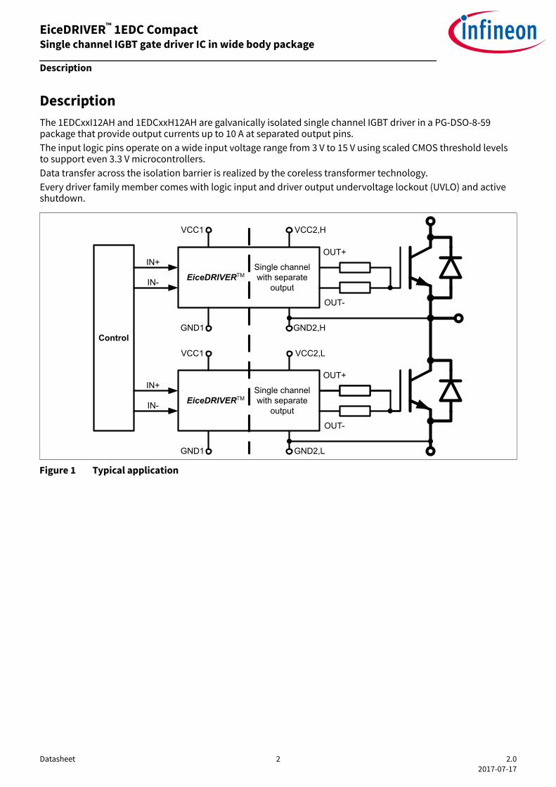
DescriptionThe 1EDCxxI12AH and 1EDCxxH12AH are galvanically isolated single channel IGBT driver in a PG-DSO-8-59package that provide output currents up to 10 A at separated output pins.The input logic pins operate on a wide input voltage range from 3 V to 15 V using scaled CMOS threshold levelsto support even 3.3 V microcontrollers.Data transfer across the isolation barrier is realized by the coreless transformer technology.Every driver family member comes with logic input and driver output undervoltage lockout (UVLO) and activeshutdown.
OUT+
OUT+
Control
EiceDRIVERTM
IN+
IN+
IN-
IN-
GND1
VCC1 VCC2,H
VCC2,L
GND2,L
GND2,HGND1
VCC1
OUT-
OUT-
Single channelwith separate
output
EiceDRIVERTMSingle channelwith separate
output
Figure 1 Typical application
EiceDRIVER™ 1EDC CompactSingle channel IGBT gate driver IC in wide body package
Description
Datasheet 2 2.02017-07-17

Table of contents
Features . . . . . . . . . . . . . . . . . . . . . . . . . . . . . . . . . . . . . . . . . . . . . . . . . . . . . . . . . . . . . . . . . . . . . . . . . . . . . . . 1
Table of contents . . . . . . . . . . . . . . . . . . . . . . . . . . . . . . . . . . . . . . . . . . . . . . . . . . . . . . . . . . . . . . . . . . . . . . . 3
1 Block diagram . . . . . . . . . . . . . . . . . . . . . . . . . . . . . . . . . . . . . . . . . . . . . . . . . . . . . . . . . . . . . . . . . . . . . . . . . . 4
2 Pin configuration and functionality . . . . . . . . . . . . . . . . . . . . . . . . . . . . . . . . . . . . . . . . . . . . . . . . . . . . . .52.1 Pin configuration . . . . . . . . . . . . . . . . . . . . . . . . . . . . . . . . . . . . . . . . . . . . . . . . . . . . . . . . . . . . . . . . . . . . . . . . 52.2 Pin functionality . . . . . . . . . . . . . . . . . . . . . . . . . . . . . . . . . . . . . . . . . . . . . . . . . . . . . . . . . . . . . . . . . . . . . . . . .5
3 Functional description . . . . . . . . . . . . . . . . . . . . . . . . . . . . . . . . . . . . . . . . . . . . . . . . . . . . . . . . . . . . . . . . . . 73.1 Introduction . . . . . . . . . . . . . . . . . . . . . . . . . . . . . . . . . . . . . . . . . . . . . . . . . . . . . . . . . . . . . . . . . . . . . . . . . . . . 73.2 Supply . . . . . . . . . . . . . . . . . . . . . . . . . . . . . . . . . . . . . . . . . . . . . . . . . . . . . . . . . . . . . . . . . . . . . . . . . . . . . . . . . 73.3 Protection features . . . . . . . . . . . . . . . . . . . . . . . . . . . . . . . . . . . . . . . . . . . . . . . . . . . . . . . . . . . . . . . . . . . . . . 83.3.1 Undervoltage lockout (UVLO) . . . . . . . . . . . . . . . . . . . . . . . . . . . . . . . . . . . . . . . . . . . . . . . . . . . . . . . . . . . 83.3.2 Active shut-down . . . . . . . . . . . . . . . . . . . . . . . . . . . . . . . . . . . . . . . . . . . . . . . . . . . . . . . . . . . . . . . . . . . . . . 83.3.3 Short circuit clamping . . . . . . . . . . . . . . . . . . . . . . . . . . . . . . . . . . . . . . . . . . . . . . . . . . . . . . . . . . . . . . . . . .83.4 Non-inverting and inverting inputs . . . . . . . . . . . . . . . . . . . . . . . . . . . . . . . . . . . . . . . . . . . . . . . . . . . . . . . . 93.5 Driver outputs . . . . . . . . . . . . . . . . . . . . . . . . . . . . . . . . . . . . . . . . . . . . . . . . . . . . . . . . . . . . . . . . . . . . . . . . . . .9
4 Electrical parameters . . . . . . . . . . . . . . . . . . . . . . . . . . . . . . . . . . . . . . . . . . . . . . . . . . . . . . . . . . . . . . . . . . 104.1 Absolute maximum ratings . . . . . . . . . . . . . . . . . . . . . . . . . . . . . . . . . . . . . . . . . . . . . . . . . . . . . . . . . . . . . . 104.2 Operating parameters . . . . . . . . . . . . . . . . . . . . . . . . . . . . . . . . . . . . . . . . . . . . . . . . . . . . . . . . . . . . . . . . . . 114.3 Electrical characteristics . . . . . . . . . . . . . . . . . . . . . . . . . . . . . . . . . . . . . . . . . . . . . . . . . . . . . . . . . . . . . . . . 114.3.1 Voltage supply . . . . . . . . . . . . . . . . . . . . . . . . . . . . . . . . . . . . . . . . . . . . . . . . . . . . . . . . . . . . . . . . . . . . . . . .114.3.2 Logic input . . . . . . . . . . . . . . . . . . . . . . . . . . . . . . . . . . . . . . . . . . . . . . . . . . . . . . . . . . . . . . . . . . . . . . . . . . . 124.3.3 Gate driver . . . . . . . . . . . . . . . . . . . . . . . . . . . . . . . . . . . . . . . . . . . . . . . . . . . . . . . . . . . . . . . . . . . . . . . . . . . 134.3.4 Short circuit clamping . . . . . . . . . . . . . . . . . . . . . . . . . . . . . . . . . . . . . . . . . . . . . . . . . . . . . . . . . . . . . . . . .144.3.5 Dynamic characteristics . . . . . . . . . . . . . . . . . . . . . . . . . . . . . . . . . . . . . . . . . . . . . . . . . . . . . . . . . . . . . . . 144.3.6 Active shut down . . . . . . . . . . . . . . . . . . . . . . . . . . . . . . . . . . . . . . . . . . . . . . . . . . . . . . . . . . . . . . . . . . . . . 15
5 Recognized under UL 1577 (File E311313) . . . . . . . . . . . . . . . . . . . . . . . . . . . . . . . . . . . . . . . . . . . . . . . 15
6 Package outline . . . . . . . . . . . . . . . . . . . . . . . . . . . . . . . . . . . . . . . . . . . . . . . . . . . . . . . . . . . . . . . . . . . . . . . 16
7 Application notes . . . . . . . . . . . . . . . . . . . . . . . . . . . . . . . . . . . . . . . . . . . . . . . . . . . . . . . . . . . . . . . . . . . . . .177.1 Reference layout for thermal data . . . . . . . . . . . . . . . . . . . . . . . . . . . . . . . . . . . . . . . . . . . . . . . . . . . . . . . . 177.2 Printed circuit board guidelines . . . . . . . . . . . . . . . . . . . . . . . . . . . . . . . . . . . . . . . . . . . . . . . . . . . . . . . . . .17
Revision history . . . . . . . . . . . . . . . . . . . . . . . . . . . . . . . . . . . . . . . . . . . . . . . . . . . . . . . . . . . . . . . . . . . . . . . 17
Trademarks . . . . . . . . . . . . . . . . . . . . . . . . . . . . . . . . . . . . . . . . . . . . . . . . . . . . . . . . . . . . . . . . . . . . . . . . . . . 18
EiceDRIVER™ 1EDC CompactSingle channel IGBT gate driver IC in wide body package
Table of contents
Datasheet 3 2.02017-07-17

1 Block diagram
IN+
IN-
GND1
VCC1
2
3
4
1
7
8
6
5
VCC2
OUT-
OUT+
GND2
inputfilter
TX
UVLO
&active filter
inputfilter
GND1
VCC1
UVLO
RX
&
Shootthrough
protection
VCC2GND2
Figure 2 Block diagram
EiceDRIVER™ 1EDC CompactSingle channel IGBT gate driver IC in wide body package
Block diagram
Datasheet 4 2.02017-07-17
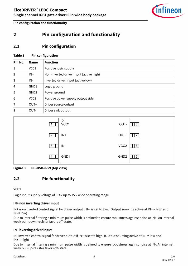
2 Pin configuration and functionality
2.1 Pin configuration
Table 1 Pin configuration
Pin No. Name Function
1 VCC1 Positive logic supply
2 IN+ Non-inverted driver input (active high)
3 IN- Inverted driver input (active low)
4 GND1 Logic ground
5 GND2 Power ground
6 VCC2 Positive power supply output side
7 OUT+ Driver source output
8 OUT- Driver sink output
1
2
3
4
8
7
6
5
VCC1
IN+
IN-
GND1
OUT-
OUT+
VCC2
GND2
Figure 3 PG-DSO-8-59 (top view)
2.2 Pin functionality
VCC1
Logic input supply voltage of 3.3 V up to 15 V wide operating range.
IN+ non inverting driver input
IN+ non-inverted control signal for driver output if IN- is set to low. (Output sourcing active at IN+ = high andIN- = low)Due to internal filtering a minimum pulse width is defined to ensure robustness against noise at IN+. An internalweak pull-down-resistor favors off-state.
IN- inverting driver input
IN- inverted control signal for driver output if IN+ is set to high. (Output sourcing active at IN- = low andIN+ = high)Due to internal filtering a minimum pulse width is defined to ensure robustness against noise at IN-. An internalweak pull-up-resistor favors off-state.
EiceDRIVER™ 1EDC CompactSingle channel IGBT gate driver IC in wide body package
Pin configuration and functionality
Datasheet 5 2.02017-07-17

GND1
Ground connection of input circuit.
GND2 reference ground
Reference ground of the output driving circuit.In case of a bipolar supply (positive and negative voltage referred to IGBT emitter) this pin is connected to thenegative supply voltage.
VCC2
Positive power supply pin of output driving circuit. A proper blocking capacitor has to be placed close to thissupply pin.
OUT+ driver source output
Driver source output pin to turn on external IGBT. During on-state the driving output is switched to VCC2.Switching of this output is controlled by IN+ and IN-. This output will also be turned off at an UVLO event.During turn off the OUT+ terminal is able to sink approx. 100 mA. In case of an unconnected OUT- the completegate charge is discharged through this channel resulting in a slow turn off.
OUT- driver sink output
Driver sink output pin to turn off external IGBT. During off-state the driving output is switched to GND2.Switching of this output is controlled by IN+ and IN-. In case of UVLO an active shut down keeps the outputvoltage at a low level.
EiceDRIVER™ 1EDC CompactSingle channel IGBT gate driver IC in wide body package
Pin configuration and functionality
Datasheet 6 2.02017-07-17
3 Functional description
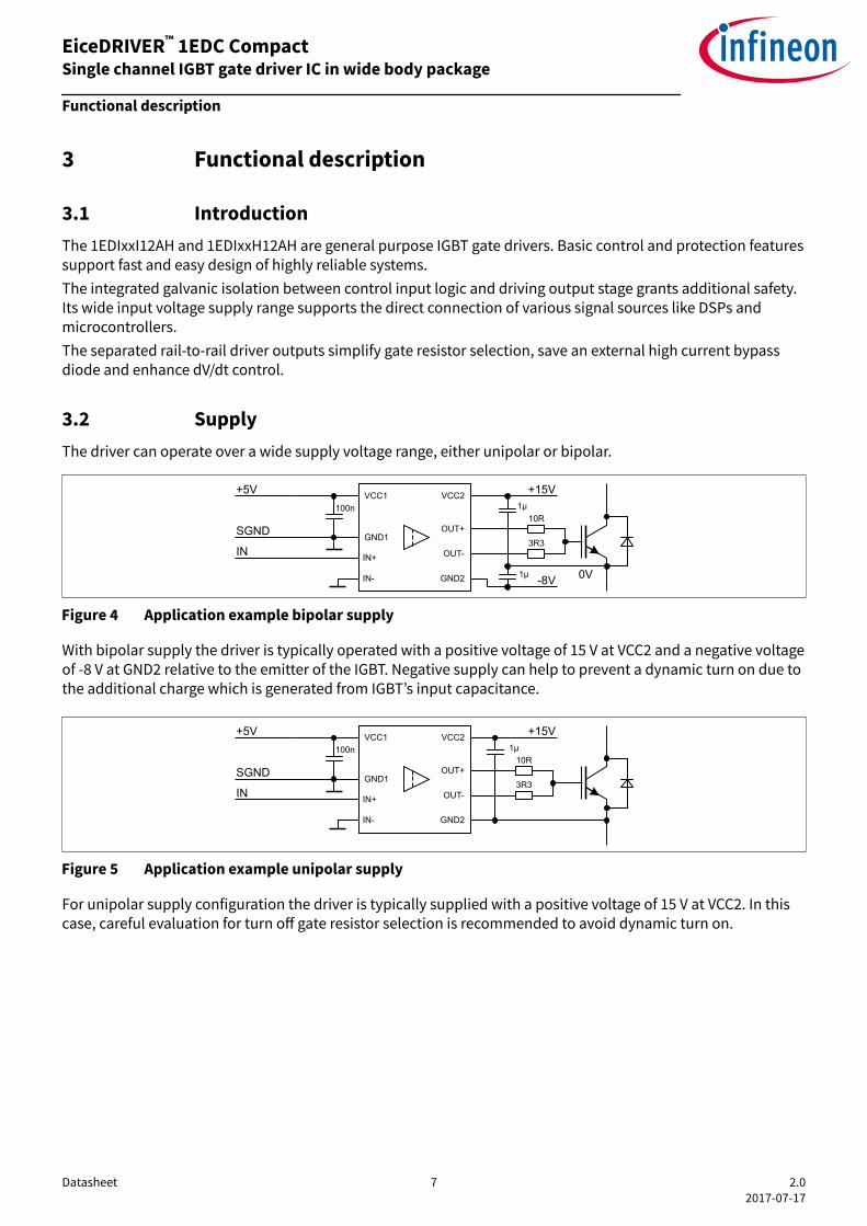
3.1 IntroductionThe 1EDIxxI12AH and 1EDIxxH12AH are general purpose IGBT gate drivers. Basic control and protection featuressupport fast and easy design of highly reliable systems.The integrated galvanic isolation between control input logic and driving output stage grants additional safety.Its wide input voltage supply range supports the direct connection of various signal sources like DSPs andmicrocontrollers.The separated rail-to-rail driver outputs simplify gate resistor selection, save an external high current bypassdiode and enhance dV/dt control.
3.2 SupplyThe driver can operate over a wide supply voltage range, either unipolar or bipolar.
GND1
IN+
IN-
VCC1
OUT+
VCC2
GND2
OUT-
+5V
SGND
IN
+15V
10R1µ100n
3R3
-8V1µ 0V
Figure 4 Application example bipolar supply
With bipolar supply the driver is typically operated with a positive voltage of 15 V at VCC2 and a negative voltageof -8 V at GND2 relative to the emitter of the IGBT. Negative supply can help to prevent a dynamic turn on due tothe additional charge which is generated from IGBT’s input capacitance.
GND1
IN+
IN-
VCC1
OUT+
VCC2
GND2
OUT-
+5V
SGND
IN
+15V
10R1µ100n
3R3
Figure 5 Application example unipolar supply
For unipolar supply configuration the driver is typically supplied with a positive voltage of 15 V at VCC2. In thiscase, careful evaluation for turn off gate resistor selection is recommended to avoid dynamic turn on.
EiceDRIVER™ 1EDC CompactSingle channel IGBT gate driver IC in wide body package
Functional description
Datasheet 7 2.02017-07-17

3.3 Protection features
3.3.1 Undervoltage lockout (UVLO)
OUT
IN+
VCC2
VCC1
VUVLOH2VUVLOL2
VUVLOH1VUVLOL1
Figure 6 UVLO behavior
To ensure correct switching of IGBTs the device is equipped with an undervoltage lockout for input and outputindependently. Operation starts only after both VCC levels have increased beyond the respective VUVLOH levels.
If the power supply voltage VVCC1 of the input chip drops below VUVLOL1 a turn-off signal is sent to the output chipbefore power-down. The IGBT is switched off and the signals at IN+ and IN- are ignored until VVCC1 reaches thepower-up voltage VUVLOH1 again.If the power supply voltage VVCC2 of the output chip goes down below VUVLOL2 the IGBT is switched off andsignals from the input chip are ignored until VVCC2 reaches the power-up voltage VUVLOH2 again.
Note: VVCC2 is always referred to GND2 and does not differentiate between unipolar or bipolar supply.
3.3.2 Active shut-downThe active shut-down feature ensures a safe IGBT off-state in case the output chip is not connected to the powersupply or an undervoltage lockout is in effect. The IGBT gate is clamped at OUT- to GND2.
3.3.3 Short circuit clampingDuring short circuit the IGBT’s gate voltage tends to rise because of the feedback via the Miller capacitance. Anadditional protection circuit connected to OUT+ limits this voltage to a value slightly higher than the supplyvoltage. A maximum current of 500 mA may be fed back to the supply through this path for 10 μs. If highercurrents are expected or tighter clamping is desired external Schottky diodes may be added.
EiceDRIVER™ 1EDC CompactSingle channel IGBT gate driver IC in wide body package
Functional description
Datasheet 8 2.02017-07-17

3.4 Non-inverting and inverting inputs
OUT
IN+
IN-
Figure 7 Logic input to output switching behavior
There are two possible input modes to control the IGBT. At non-inverting mode IN+ controls the driver outputwhile IN- is set to low. At inverting mode IN- controls the driver output while IN+ is set to high. A minimum inputpulse width is defined to filter occasional glitches.
3.5 Driver outputsThe output driver section uses MOSFETs to provide a rail-to-rail output. This feature permits that tight control ofgate voltage during on-state and short circuit can be maintained as long as the driver’s supply is stable. Due tothe low internal voltage drop, switching behavior of the IGBT is predominantly governed by the gate resistor.Furthermore, it reduces the power to be dissipated by the driver.
EiceDRIVER™ 1EDC CompactSingle channel IGBT gate driver IC in wide body package
Functional description
Datasheet 9 2.02017-07-17
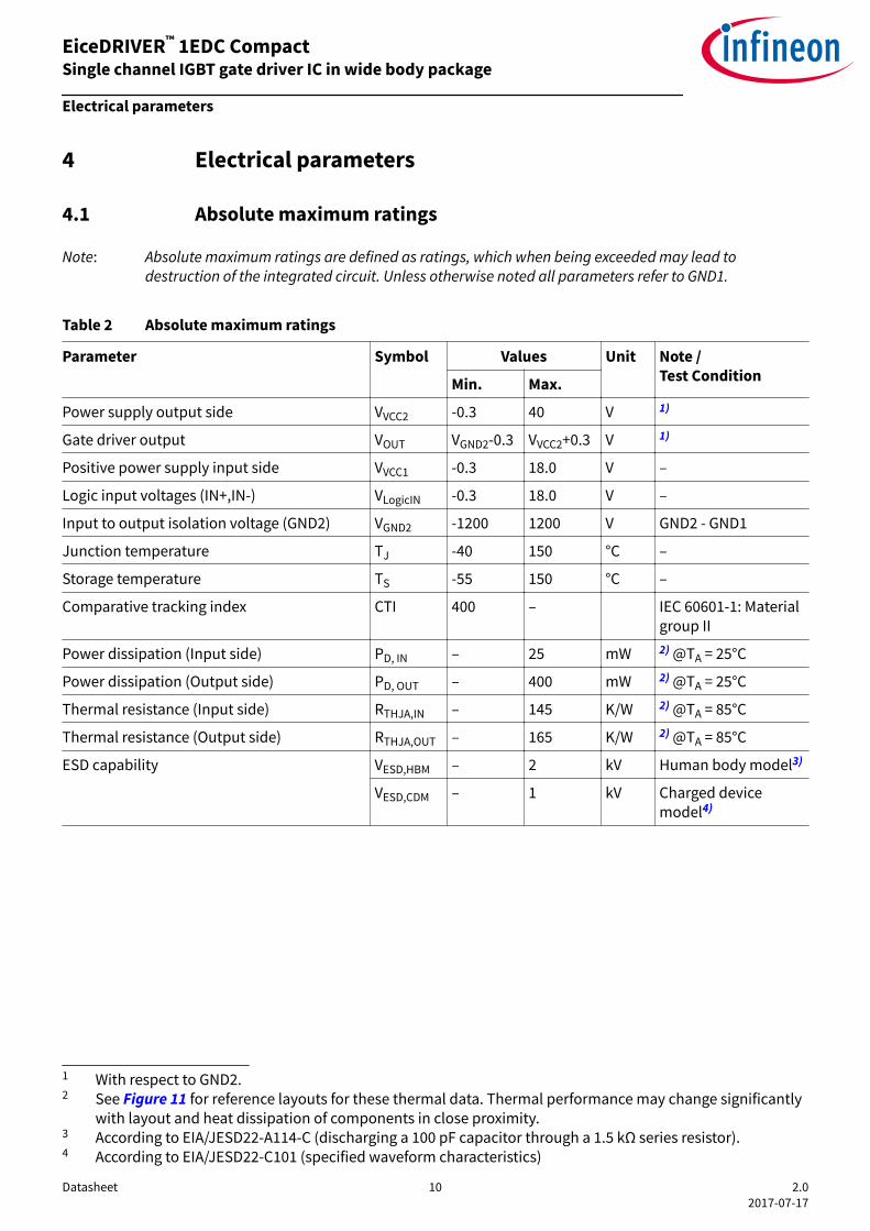
4 Electrical parameters
4.1 Absolute maximum ratings
Note: Absolute maximum ratings are defined as ratings, which when being exceeded may lead todestruction of the integrated circuit. Unless otherwise noted all parameters refer to GND1.
Table 2 Absolute maximum ratings
Parameter Symbol Values Unit Note /Test ConditionMin. Max.
Power supply output side VVCC2 -0.3 40 V 1)
Gate driver output VOUT VGND2-0.3 VVCC2+0.3 V 1)
Positive power supply input side VVCC1 -0.3 18.0 V –
Logic input voltages (IN+,IN-) VLogicIN -0.3 18.0 V –
Input to output isolation voltage (GND2) VGND2 -1200 1200 V GND2 - GND1
Junction temperature TJ -40 150 °C –
Storage temperature TS -55 150 °C –
Comparative tracking index CTI 400 – IEC 60601-1: Materialgroup II
Power dissipation (Input side) PD, IN – 25 mW 2) @TA = 25°C
Power dissipation (Output side) PD, OUT – 400 mW 2) @TA = 25°C
Thermal resistance (Input side) RTHJA,IN – 145 K/W 2) @TA = 85°C
Thermal resistance (Output side) RTHJA,OUT – 165 K/W 2) @TA = 85°C
ESD capability VESD,HBM – 2 kV Human body model3)
VESD,CDM – 1 kV Charged devicemodel4)
1 With respect to GND2.2 See Figure 11 for reference layouts for these thermal data. Thermal performance may change significantly
with layout and heat dissipation of components in close proximity.3 According to EIA/JESD22-A114-C (discharging a 100 pF capacitor through a 1.5 kΩ series resistor).4 According to EIA/JESD22-C101 (specified waveform characteristics)
EiceDRIVER™ 1EDC CompactSingle channel IGBT gate driver IC in wide body package
Electrical parameters
Datasheet 10 2.02017-07-17

4.2 Operating parameters
Note: Within the operating range the IC operates as described in the functional description. Unlessotherwise noted all parameters refer to GND1.
Table 3 Operating parameters
Parameter Symbol Values Unit Note /Test ConditionMin. Max.
Power supply output side VVCC2 13 35 V 5)
Power supply input side VVCC1 3.1 17 V –
Logic input voltages (IN+,IN-) VLogicIN -0.3 17 V –
Switching frequency fsw – 1.0 MHz 6)7)
Ambient temperature TA -40 125 °C –
Thermal coefficient, junction-top Ψth,jt – 4.8 K/W 7) at TA = 85°C
Common mode transient immunity (CMTI) |dVISO/dt| – 100 kV/μs 7) at 1000 V
4.3 Electrical characteristics
Note: The electrical characteristics include the spread of values in supply voltages, load and junctiontemperatures given below. Typical values represent the median values at TA = 25°C. Unless otherwisenoted all voltages are given with respect to their respective GND (GND1 for pins 1 to 3, GND2 for pins 6to 8).
4.3.1 Voltage supply
Table 4 Voltage supply
Parameter Symbol Values Unit Note or TestConditionMin. Typ. Max.
UVLO threshold input chip VUVLOH1 – 2.85 3.1 V –
VUVLOL1 2.55 2.75 – V –
UVLO hysteresis input chip(VUVLOH1 - VUVLOL1)
VHYS1 0.09 0.1 – V –
UVLO threshold output chip (IGBTsupply)
VUVLOH2 – 12.0 12.7 V 8)
VUVLOL2 10.5 11.1 – V 8)
5 With respect to GND2.6 do not exceed max. power dissipation7 Parameter is not subject to production test - verified by design/characterization8 With respect to GND2.
EiceDRIVER™ 1EDC CompactSingle channel IGBT gate driver IC in wide body package
Electrical parameters
Datasheet 11 2.02017-07-17

Table 4 Voltage supply (continued)
Parameter Symbol Values Unit Note or TestConditionMin. Typ. Max.
UVLO hysteresis output chip(VUVLOH2 - VUVLOL2)
VHYS2 0.7 0.85 – V –
Quiescent current input chip IQ1 – 0.65 1.0 mA VVCC1 = 5 VIN+ = High, IN- = Low=>OUT = High
Quiescent current output chip IQ2 – 1.2 2.0 mA VVCC2 = 15 VIN+ = High, IN- = Low=>OUT = High
4.3.2 Logic input
UVLO
No driver operation
5 10 15 VVCC1
VIN+L ,VIN-L
VIN+H ,VIN-H
5
10
V VCC
1,m
ax
0.7×5V
0.3×5V
0.7×15V
0.3×15V
3.3
IN+, IN- Low Input Voltage, max
0.3×3.3V
IN+,IN- High Input Voltage, min
0.7×3.3V
Figure 8 VCC1 scaled input threshold voltage of IN+ and IN-
Beginning from the input undervoltage lockout level, threshold levels for IN+ and IN- are scaled to VVCC1. Thehigh input threshold is 70% of VVCC1 and the low input threshold is at 30% of VVCC1.
Table 5 Logic input
Parameter Symbol Values Unit Note or TestConditionMin. Typ. Max.
IN+,IN- low input voltage VIN+L,VIN-L
– – 0.3 ×VVCC1
9)3.1 V ≤ VVCC1 ≤ 17 V
IN+,IN- high input voltage VIN+H,VIN-H
0.7 ×VVCC1
– –
9 Parameter is not subject to production test - verified by design/characterization
EiceDRIVER™ 1EDC CompactSingle channel IGBT gate driver IC in wide body package
Electrical parameters
Datasheet 12 2.02017-07-17

Table 5 Logic input (continued)
Parameter Symbol Values Unit Note or TestConditionMin. Typ. Max.
IN+,IN- low input voltage VIN+L,VIN-L
– – 1.5 V VVCC1 = 5.0 V
IN+,IN- high input voltage VIN+H,VIN-H
3.5 – – V
IN- input current IIN- – 70 200 μA VVCC1 = 5.0 V, VIN- =GND1
IN+ input current IIN+ – 70 200 μA VVCC1 = 5.0 V, VIN+ =VVCC1
4.3.3 Gate driver
Note: minimum Peak current rating valid over temperature range!
Table 6 Gate driver
Parameter Symbol Values Unit Note or TestConditionMin. Typ. Max.
High level output peak current(source)1EDC05I12AH1EDC20I12AH1EDC20H12AH1EDC40I12AH1EDC60I12AH1EDC60H12AH
IOUT+,PEAK
0.52.02.04.06.06.0
1.34.04.07.510.010.0
– A 10)IN+ = High,IN- = Low,VVCC2 = 15 V
Low level output peak current(sink)1EDC05I12AH1EDC20I12AH1EDC20H12AH1EDC40I12AH1EDC60I12AH1EDC60H12AH
IOUT-,PEAK
0.52.02.04.06.06.0
0.93.53.56.89.49.4
– A 10)IN+ = Low,IN- = Low,VVCC2 = 15 V
10 specified min. output current is forced; voltage across the device V(VCC2 - OUT+) or V(OUT- - GND2) < VVCC2.
EiceDRIVER™ 1EDC CompactSingle channel IGBT gate driver IC in wide body package
Electrical parameters
Datasheet 13 2.02017-07-17

4.3.4 Short circuit clamping
Table 7 Short circuit clamping
Parameter Symbol Values Unit Note or TestConditionMin. Typ. Max.
Clamping voltage (OUT+)(VOUT+ - VVCC2)
VCLPout – 0.9 1.3 V 11)IN+ = High, IN- =Low,OUT = HighIOUT = 500 mA,(pulse test tCLPmax =10 μs)
4.3.5 Dynamic characteristicsDynamic characteristics are measured with VVCC1 = 5 V and VVCC2 = 15 V.
IN+
OUTTPDON
50%
50%
TPDOFF
20%
80%
TRISE TFALL
Figure 9 Propagation delay, rise and fall time
Table 8 Dynamic characteristics
Parameter Symbol Values Unit Note or TestConditionMin. Typ. Max.
Input IN to output propagationdelay ON
TPDON 270 300 330 ns CLOAD = 100 pFVIN+ = 50%,VOUT=50% @25°C1EDC05I12AH,1EDC20I12AH,1EDC40I12AH,1EDC60I12AH
Input IN to output propagationdelay OFF
TPDOFF 270 300 330 ns
Input IN to output propagationdelay distortion (TPDOFF - TPDON)
TPDISTO -30 5 40 ns
Input pulse suppression time IN+,IN-
TMININ+,TMININ-
230 240 – ns
11 With respect to GND2.
EiceDRIVER™ 1EDC CompactSingle channel IGBT gate driver IC in wide body package
Electrical parameters
Datasheet 14 2.02017-07-17

Table 8 Dynamic characteristics (continued)
Parameter Symbol Values Unit Note or TestConditionMin. Typ. Max.
Input IN to output propagationdelay ON
TPDON 95 120 142 ns CLOAD = 100 pFVIN+ = 50%,VOUT=50% @25°C1EDC20H12AH,1EDC60H12AH
Input IN to output propagationdelay OFF
TPDOFF 105 125 150 ns
Input IN to output propagationdelay distortion (TPDOFF - TPDON)
TPDISTO -35 -5 25 ns
Input Pulse Suppressiontime IN+,IN-
TMININ+,TMININ-
30 40 – ns
Input IN to output propagationdelay ON variation due to temp
TPDONt – – 14 ns 12)CLOAD = 100 pFVIN+ = 50%,VOUT=50%Input IN to output propagation
delay OFF variation due to tempTPDONt – – 14 ns
Input IN to output propagationdelay distortion variation due totemp (TPDOFF-TPDON)
TPDISTOt – – 8 ns
Rise time TRISE 5 10 20 ns CLOAD = 1 nFVL20%, VH 80%Fall time TFALL 4 9 19 ns
4.3.6 Active shut down
Table 9 Active shut down
Parameter Symbol Values Unit Note or TestConditionMin. Typ. Max.
Active shut down voltage VACTSD – 2.0 2.3 V 13)IOUT-/IOUT-,PEAK=0.1,VCC2 open
5 Recognized under UL 1577 (File E311313)
Table 10 Recognized under UL 1577
Description Symbol Characteristic UnitInsulation Withstand Voltage / 1 min VISO 2500 Vrms
Insulation Test Voltage / 1 s VISO 3000 Vrms
12 Parameter is not subject to production test - verified by design/characterization13 With respect to GND2.
EiceDRIVER™ 1EDC CompactSingle channel IGBT gate driver IC in wide body package
Recognized under UL 1577 (File E311313)
Datasheet 15 2.02017-07-17

6 Package outline
0.252
0.104
0.020
0.013
0.417
0.299
0.035
0.018
MILLIMETERS
L
h
ccc
ddd
D
DIM
A2
A
b
c
E
E1
N
e
-
MIN
8
0.020
0.004
0.010
0.010
2.45
MAX
INCHES
8
0.050 BSC
0.244
MIN
-
0.089
0.012
0.009
0.394
0.291
MAX
0.096
SCALE
20
4mm
0
2
2.25
2.65
0.50
0.32
6.40
10.60
7.607.40
10.00
6.20
0.23
0.30
0.900.50
0.450.25
0.25
0.10
1.27 BSC
01
ISSUE DATE
05.11.2015
DOCUMENT NO.
Z8B00179262
EUROPEAN PROJECTION
REVISION
A1 0.20 0.004 0.0080.10
Θ 0° 8°8°0°
L2 0.25 BSC 0.010 BSC
Figure 10 PG-DSO-8-59 (Plastic (green) dual small outline package)
EiceDRIVER™ 1EDC CompactSingle channel IGBT gate driver IC in wide body package
Package outline
Datasheet 16 2.02017-07-17
7 Application notes
7.1 Reference layout for thermal data
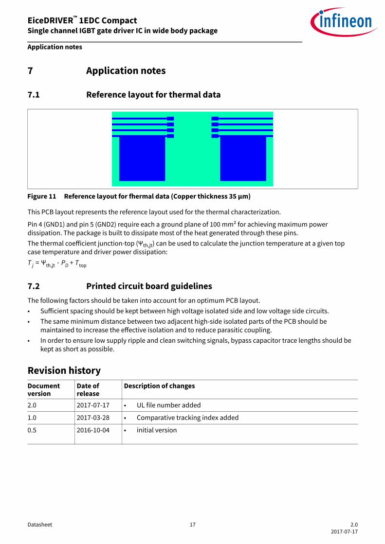
Figure 11 Reference layout for fhermal data (Copper thickness 35 μm)
This PCB layout represents the reference layout used for the thermal characterization.
Pin 4 (GND1) and pin 5 (GND2) require each a ground plane of 100 mm² for achieving maximum powerdissipation. The package is built to dissipate most of the heat generated through these pins.The thermal coefficient junction-top (Ψth,jt) can be used to calculate the junction temperature at a given topcase temperature and driver power dissipation:T j = Ψth,jt ⋅ PD + Ttop
7.2 Printed circuit board guidelinesThe following factors should be taken into account for an optimum PCB layout.• Sufficient spacing should be kept between high voltage isolated side and low voltage side circuits.• The same minimum distance between two adjacent high-side isolated parts of the PCB should be
maintained to increase the effective isolation and to reduce parasitic coupling.• In order to ensure low supply ripple and clean switching signals, bypass capacitor trace lengths should be
kept as short as possible.
Revision historyDocumentversion
Date ofrelease
Description of changes
2.0 2017-07-17 • UL file number added
1.0 2017-03-28 • Comparative tracking index added
0.5 2016-10-04 • initial version
EiceDRIVER™ 1EDC CompactSingle channel IGBT gate driver IC in wide body package
Application notes
Datasheet 17 2.02017-07-17

TrademarksAll referenced product or service names and trademarks are the property of their respective owners.
Edition 2017-07-17Published byInfineon Technologies AG81726 Munich, Germany © 2017 Infineon Technologies AGAll Rights Reserved. Do you have a question about anyaspect of this document?Email: [email protected] Document referenceIFX-acq1467706781217
IMPORTANT NOTICEThe information given in this document shall in noevent be regarded as a guarantee of conditions orcharacteristics (“Beschaffenheitsgarantie”) .With respect to any examples, hints or any typical valuesstated herein and/or any information regarding theapplication of the product, Infineon Technologieshereby disclaims any and all warranties and liabilities ofany kind, including without limitation warranties ofnon-infringement of intellectual property rights of anythird party.In addition, any information given in this document issubject to customer’s compliance with its obligationsstated in this document and any applicable legalrequirements, norms and standards concerningcustomer’s products and any use of the product ofInfineon Technologies in customer’s applications.The data contained in this document is exclusivelyintended for technically trained staff. It is theresponsibility of customer’s technical departments toevaluate the suitability of the product for the intendedapplication and the completeness of the productinformation given in this document with respect to suchapplication.
WARNINGSDue to technical requirements products may containdangerous substances. For information on the typesin question please contact your nearest InfineonTechnologies office.Except as otherwise explicitly approved by InfineonTechnologies in a written document signed byauthorized representatives of Infineon Technologies,Infineon Technologies’ products may not be used inany applications where a failure of the product orany consequences of the use thereof can reasonablybe expected to result in personal injury