Embed Size (px)
Citation preview

ATV PTS HVD
Data SheetHardware DescriptionRev 2.0, 2017-06-19
1EDI2010ASSingle Channel Isolated Driver
E iceDRIVER™ SENSEHigh Voltage IGBT Driver for Automotive Applications

Edition 2017-06-19Published byInfineon Technologies AG81726 Munich, Germany© 2017 Infineon Technologies AGAll Rights Reserved.
Legal DisclaimerThe information given in this document shall in no event be regarded as a guarantee of conditions or characteristics. With respect to any examples or hints given herein, any typical values stated herein and/or any information regarding the application of the device, Infineon Technologies hereby disclaims any and all warranties and liabilities of any kind, including without limitation, warranties of non-infringement of intellectual property rights of any third party.
InformationFor further information on technology, delivery terms and conditions and prices, please contact the nearest Infineon Technologies Office (www.infineon.com).
WarningsDue to technical requirements, components may contain dangerous substances. For information on the types in question, please contact the nearest Infineon Technologies Office.Infineon Technologies components may be used in life-support devices or systems only with the express written approval of Infineon Technologies, if a failure of such components can reasonably be expected to cause the failure of that life-support device or system or to affect the safety or effectiveness of that device or system. Life support devices or systems are intended to be implanted in the human body or to support and/or maintain and sustain and/or protect human life. If they fail, it is reasonable to assume that the health of the user or other persons may be endangered.

EiceDRIVER™ SENSE1EDI2010AS
Data Sheet 3 Rev 2.0, 2017-06-19Hardware Description
Trademarks of Infineon Technologies AGAURIX™, C166™, CanPAK™, CIPOS™, CIPURSE™, EconoPACK™, CoolMOS™, CoolSET™,CORECONTROL™, CROSSAVE™, DAVE™, EasyPIM™, EconoBRIDGE™, EconoDUAL™, EconoPIM™,EiceDRIVER™, eupec™, FCOS™, HITFET™, HybridPACK™, I²RF™, ISOFACE™, IsoPACK™, MIPAQ™,ModSTACK™, my-d™, NovalithIC™, OptiMOS™, ORIGA™, PRIMARION™, PrimePACK™, PrimeSTACK™,PRO-SIL™, PROFET™, RASIC™, ReverSave™, SatRIC™, SIEGET™, SINDRION™, SIPMOS™,SmartLEWIS™, SOLID FLASH™, TEMPFET™, thinQ!™, TRENCHSTOP™, TriCore™.
Other TrademarksAdvance Design System™ (ADS) of Agilent Technologies, AMBA™, ARM™, MULTI-ICE™, KEIL™,PRIMECELL™, REALVIEW™, THUMB™, µVision™ of ARM Limited, UK. AUTOSAR™ is licensed by AUTOSARdevelopment partnership. Bluetooth™ of Bluetooth SIG Inc. CAT-iq™ of DECT Forum. COLOSSUS™,FirstGPS™ of Trimble Navigation Ltd. EMV™ of EMVCo, LLC (Visa Holdings Inc.). EPCOS™ of Epcos AG.FLEXGO™ of Microsoft Corporation. FlexRay™ is licensed by FlexRay Consortium. HYPERTERMINAL™ ofHilgraeve Incorporated. IEC™ of Commission Electrotechnique Internationale. IrDA™ of Infrared DataAssociation Corporation. ISO™ of INTERNATIONAL ORGANIZATION FOR STANDARDIZATION. MATLAB™ ofMathWorks, Inc. MAXIM™ of Maxim Integrated Products, Inc. MICROTEC™, NUCLEUS™ of Mentor GraphicsCorporation. Mifare™ of NXP. MIPI™ of MIPI Alliance, Inc. MIPS™ of MIPS Technologies, Inc., USA. muRata™of MURATA MANUFACTURING CO., MICROWAVE OFFICE™ (MWO) of Applied Wave Research Inc.,OmniVision™ of OmniVision Technologies, Inc. Openwave™ Openwave Systems Inc. RED HAT™ Red Hat, Inc.RFMD™ RF Micro Devices, Inc. SIRIUS™ of Sirius Satellite Radio Inc. SOLARIS™ of Sun Microsystems, Inc.SPANSION™ of Spansion LLC Ltd. Symbian™ of Symbian Software Limited. TAIYO YUDEN™ of Taiyo YudenCo. TEAKLITE™ of CEVA, Inc. TEKTRONIX™ of Tektronix Inc. TOKO™ of TOKO KABUSHIKI KAISHA TA.UNIX™ of X/Open Company Limited. VERILOG™, PALLADIUM™ of Cadence Design Systems, Inc. VLYNQ™of Texas Instruments Incorporated. VXWORKS™, WIND RIVER™ of WIND RIVER SYSTEMS, INC. ZETEX™ ofDiodes Zetex Limited.Last Trademarks Update 2011-02-24
Revision HistoryPage or Item Subjects (major changes since previous revision)Rev 1.3.3, 2017-01-27 Page 49 New chapter with Failure behavior 2.4.9.4 (former reset events) Page 50 Reset Events Summary table updated due to new chapter 2.4.9.4 Table 2-15 Page 22 Updated figure 2-7. Page 124 GATE pin characteristics merged in Table 5-11 with TON/TOFF characteristics. Page 124 Added test conditions in Table 5-11 for TON/TOFF & GATE pin. Page 124 Merged VPCLPG and VPCLP in Table 5-11 due to test conditions. Same for IPCLP. Page 124 Removed unprecise footnote in Table 5-11. Page 113 Updated values for weak pull down in Table 5-12. Page 128 Moved DESAT input voltage range to DESAT characteristics in Table 5-16. Page 39 Updated Links of Registers in Chapter 2.4.6.1 and 2.4.6.2.
EiceDRIVER™ SENSE1EDI2010AS
Table of Contents
Data Sheet 4 Rev 2.0, 2017-06-19Hardware Description
Table of Contents . . . . . . . . . . . . . . . . . . . . . . . . . . . . . . . . . . . . . . . . . . . . . . . . . . . . . . . . . . . . . . . . 4
List of Figures . . . . . . . . . . . . . . . . . . . . . . . . . . . . . . . . . . . . . . . . . . . . . . . . . . . . . . . . . . . . . . . . . . . 7
List of Tables . . . . . . . . . . . . . . . . . . . . . . . . . . . . . . . . . . . . . . . . . . . . . . . . . . . . . . . . . . . . . . . . . . . . 8
1 Product Definition . . . . . . . . . . . . . . . . . . . . . . . . . . . . . . . . . . . . . . . . . . . . . . . . . . . . . . . . . . . . . . . 101.1 Overview . . . . . . . . . . . . . . . . . . . . . . . . . . . . . . . . . . . . . . . . . . . . . . . . . . . . . . . . . . . . . . . . . . . . . . . 101.2 Feature Overview . . . . . . . . . . . . . . . . . . . . . . . . . . . . . . . . . . . . . . . . . . . . . . . . . . . . . . . . . . . . . . . . 101.3 Target Applications . . . . . . . . . . . . . . . . . . . . . . . . . . . . . . . . . . . . . . . . . . . . . . . . . . . . . . . . . . . . . . . 11
2 Functional Description . . . . . . . . . . . . . . . . . . . . . . . . . . . . . . . . . . . . . . . . . . . . . . . . . . . . . . . . . . . 122.1 Introduction . . . . . . . . . . . . . . . . . . . . . . . . . . . . . . . . . . . . . . . . . . . . . . . . . . . . . . . . . . . . . . . . . . . . . 122.2 Pin Configuration and Functionality . . . . . . . . . . . . . . . . . . . . . . . . . . . . . . . . . . . . . . . . . . . . . . . . . . 132.2.1 Pin Configuration . . . . . . . . . . . . . . . . . . . . . . . . . . . . . . . . . . . . . . . . . . . . . . . . . . . . . . . . . . . . . . . 132.2.2 Pin Functionality . . . . . . . . . . . . . . . . . . . . . . . . . . . . . . . . . . . . . . . . . . . . . . . . . . . . . . . . . . . . . . . 152.2.2.1 Primary Side . . . . . . . . . . . . . . . . . . . . . . . . . . . . . . . . . . . . . . . . . . . . . . . . . . . . . . . . . . . . . . . . 152.2.2.2 Secondary Side . . . . . . . . . . . . . . . . . . . . . . . . . . . . . . . . . . . . . . . . . . . . . . . . . . . . . . . . . . . . . . 162.2.2.3 Pull Devices . . . . . . . . . . . . . . . . . . . . . . . . . . . . . . . . . . . . . . . . . . . . . . . . . . . . . . . . . . . . . . . . . 172.3 Block Diagram . . . . . . . . . . . . . . . . . . . . . . . . . . . . . . . . . . . . . . . . . . . . . . . . . . . . . . . . . . . . . . . . . . 192.4 Functional Block Description . . . . . . . . . . . . . . . . . . . . . . . . . . . . . . . . . . . . . . . . . . . . . . . . . . . . . . . 202.4.1 Power Supplies . . . . . . . . . . . . . . . . . . . . . . . . . . . . . . . . . . . . . . . . . . . . . . . . . . . . . . . . . . . . . . . . 202.4.2 Clock Domains . . . . . . . . . . . . . . . . . . . . . . . . . . . . . . . . . . . . . . . . . . . . . . . . . . . . . . . . . . . . . . . . . 202.4.3 PWM Input Stage . . . . . . . . . . . . . . . . . . . . . . . . . . . . . . . . . . . . . . . . . . . . . . . . . . . . . . . . . . . . . . . 212.4.4 SPI Interface . . . . . . . . . . . . . . . . . . . . . . . . . . . . . . . . . . . . . . . . . . . . . . . . . . . . . . . . . . . . . . . . . . 232.4.4.1 Overview . . . . . . . . . . . . . . . . . . . . . . . . . . . . . . . . . . . . . . . . . . . . . . . . . . . . . . . . . . . . . . . . . . . 232.4.4.2 General Operation . . . . . . . . . . . . . . . . . . . . . . . . . . . . . . . . . . . . . . . . . . . . . . . . . . . . . . . . . . . . 242.4.4.3 Definitions . . . . . . . . . . . . . . . . . . . . . . . . . . . . . . . . . . . . . . . . . . . . . . . . . . . . . . . . . . . . . . . . . . 262.4.4.4 SPI Data Integrity Support . . . . . . . . . . . . . . . . . . . . . . . . . . . . . . . . . . . . . . . . . . . . . . . . . . . . . . 282.4.4.4.1 Parity Bit . . . . . . . . . . . . . . . . . . . . . . . . . . . . . . . . . . . . . . . . . . . . . . . . . . . . . . . . . . . . . . . . . . 282.4.4.4.2 SPI Error . . . . . . . . . . . . . . . . . . . . . . . . . . . . . . . . . . . . . . . . . . . . . . . . . . . . . . . . . . . . . . . . . . 282.4.4.5 Protocol Description . . . . . . . . . . . . . . . . . . . . . . . . . . . . . . . . . . . . . . . . . . . . . . . . . . . . . . . . . . . 292.4.4.5.1 Command Catalog . . . . . . . . . . . . . . . . . . . . . . . . . . . . . . . . . . . . . . . . . . . . . . . . . . . . . . . . . . 292.4.4.5.2 Word Convention . . . . . . . . . . . . . . . . . . . . . . . . . . . . . . . . . . . . . . . . . . . . . . . . . . . . . . . . . . . 292.4.4.5.3 ENTER_CMODE Command . . . . . . . . . . . . . . . . . . . . . . . . . . . . . . . . . . . . . . . . . . . . . . . . . . 302.4.4.5.4 ENTER_VMODE Command . . . . . . . . . . . . . . . . . . . . . . . . . . . . . . . . . . . . . . . . . . . . . . . . . . . 302.4.4.5.5 EXIT_CMODE Command . . . . . . . . . . . . . . . . . . . . . . . . . . . . . . . . . . . . . . . . . . . . . . . . . . . . . 302.4.4.5.6 NOP Command . . . . . . . . . . . . . . . . . . . . . . . . . . . . . . . . . . . . . . . . . . . . . . . . . . . . . . . . . . . . 312.4.4.5.7 READ Command . . . . . . . . . . . . . . . . . . . . . . . . . . . . . . . . . . . . . . . . . . . . . . . . . . . . . . . . . . . 312.4.4.5.8 WRITEH . . . . . . . . . . . . . . . . . . . . . . . . . . . . . . . . . . . . . . . . . . . . . . . . . . . . . . . . . . . . . . . . . . 312.4.4.5.9 WRITEL . . . . . . . . . . . . . . . . . . . . . . . . . . . . . . . . . . . . . . . . . . . . . . . . . . . . . . . . . . . . . . . . . . 322.4.5 Operating Modes . . . . . . . . . . . . . . . . . . . . . . . . . . . . . . . . . . . . . . . . . . . . . . . . . . . . . . . . . . . . . . . 332.4.5.1 General Operation . . . . . . . . . . . . . . . . . . . . . . . . . . . . . . . . . . . . . . . . . . . . . . . . . . . . . . . . . . . . 332.4.5.2 Definitions . . . . . . . . . . . . . . . . . . . . . . . . . . . . . . . . . . . . . . . . . . . . . . . . . . . . . . . . . . . . . . . . . . 342.4.5.2.1 Events and State Transitions . . . . . . . . . . . . . . . . . . . . . . . . . . . . . . . . . . . . . . . . . . . . . . . . . . 342.4.5.2.2 Emergency Turn-Off Sequence . . . . . . . . . . . . . . . . . . . . . . . . . . . . . . . . . . . . . . . . . . . . . . . . 352.4.5.2.3 Ready, Disabled, Enabled and Active State . . . . . . . . . . . . . . . . . . . . . . . . . . . . . . . . . . . . . . . 352.4.5.3 Operation Modes Description . . . . . . . . . . . . . . . . . . . . . . . . . . . . . . . . . . . . . . . . . . . . . . . . . . . 362.4.5.4 Activating the device after reset . . . . . . . . . . . . . . . . . . . . . . . . . . . . . . . . . . . . . . . . . . . . . . . . . . 372.4.5.5 Activating the device after an Event Class A or B . . . . . . . . . . . . . . . . . . . . . . . . . . . . . . . . . . . . 372.4.5.6 Debug Mode . . . . . . . . . . . . . . . . . . . . . . . . . . . . . . . . . . . . . . . . . . . . . . . . . . . . . . . . . . . . . . . . 38
Table of Contents

EiceDRIVER™ SENSE1EDI2010AS
Table of Contents
Data Sheet 5 Rev 2.0, 2017-06-19Hardware Description
2.4.6 Driver Functionality . . . . . . . . . . . . . . . . . . . . . . . . . . . . . . . . . . . . . . . . . . . . . . . . . . . . . . . . . . . . . 392.4.6.1 Overview . . . . . . . . . . . . . . . . . . . . . . . . . . . . . . . . . . . . . . . . . . . . . . . . . . . . . . . . . . . . . . . . . . . 392.4.6.2 Switching Sequence Description . . . . . . . . . . . . . . . . . . . . . . . . . . . . . . . . . . . . . . . . . . . . . . . . 442.4.6.3 Passive Clamping . . . . . . . . . . . . . . . . . . . . . . . . . . . . . . . . . . . . . . . . . . . . . . . . . . . . . . . . . . . . 462.4.7 Fault Notifications . . . . . . . . . . . . . . . . . . . . . . . . . . . . . . . . . . . . . . . . . . . . . . . . . . . . . . . . . . . . . . 462.4.8 EN Signal Pin . . . . . . . . . . . . . . . . . . . . . . . . . . . . . . . . . . . . . . . . . . . . . . . . . . . . . . . . . . . . . . . . . 472.4.9 Internal Supervision . . . . . . . . . . . . . . . . . . . . . . . . . . . . . . . . . . . . . . . . . . . . . . . . . . . . . . . . . . . . . 482.4.9.1 Lifesign watchdog . . . . . . . . . . . . . . . . . . . . . . . . . . . . . . . . . . . . . . . . . . . . . . . . . . . . . . . . . . . . 482.4.9.2 Oscillator Monitoring . . . . . . . . . . . . . . . . . . . . . . . . . . . . . . . . . . . . . . . . . . . . . . . . . . . . . . . . . . 482.4.9.3 Memory Supervision . . . . . . . . . . . . . . . . . . . . . . . . . . . . . . . . . . . . . . . . . . . . . . . . . . . . . . . . . . 482.4.9.4 Hardware Failure Behavior . . . . . . . . . . . . . . . . . . . . . . . . . . . . . . . . . . . . . . . . . . . . . . . . . . . . . 492.4.10 Reset Events . . . . . . . . . . . . . . . . . . . . . . . . . . . . . . . . . . . . . . . . . . . . . . . . . . . . . . . . . . . . . . . . . . 502.4.11 Operation in Configuration Mode . . . . . . . . . . . . . . . . . . . . . . . . . . . . . . . . . . . . . . . . . . . . . . . . . . . 512.4.11.1 Static Configuration Parameters . . . . . . . . . . . . . . . . . . . . . . . . . . . . . . . . . . . . . . . . . . . . . . . . . 512.4.11.1.1 Configuration of the SPI Parity Check . . . . . . . . . . . . . . . . . . . . . . . . . . . . . . . . . . . . . . . . . . . 512.4.11.1.2 Configuration of NFLTA and NFLTB clear mode . . . . . . . . . . . . . . . . . . . . . . . . . . . . . . . . . . . 512.4.11.1.3 Configuration of NFLTA activation in case of Boundary Check event . . . . . . . . . . . . . . . . . . . 512.4.11.1.4 Configuration of pin ADCT . . . . . . . . . . . . . . . . . . . . . . . . . . . . . . . . . . . . . . . . . . . . . . . . . . . . 512.4.11.1.5 Configuration of the STP Minimum Dead Time . . . . . . . . . . . . . . . . . . . . . . . . . . . . . . . . . . . . 522.4.11.1.6 Configuration of the Digital Channel . . . . . . . . . . . . . . . . . . . . . . . . . . . . . . . . . . . . . . . . . . . . . 522.4.11.1.7 Configuration of the VBE Compensation . . . . . . . . . . . . . . . . . . . . . . . . . . . . . . . . . . . . . . . . . . 522.4.11.1.8 Clamping of DESAT pin . . . . . . . . . . . . . . . . . . . . . . . . . . . . . . . . . . . . . . . . . . . . . . . . . . . . . . 522.4.11.1.9 Activation of the Pulse Suppressor . . . . . . . . . . . . . . . . . . . . . . . . . . . . . . . . . . . . . . . . . . . . . 522.4.11.1.10 Configuration of the Verification Mode Time Out Duration . . . . . . . . . . . . . . . . . . . . . . . . . . . 522.4.11.1.11 DESAT Threshold Level Configuration . . . . . . . . . . . . . . . . . . . . . . . . . . . . . . . . . . . . . . . . . . 522.4.11.1.12 UVLO2 Threshold Level Configuration . . . . . . . . . . . . . . . . . . . . . . . . . . . . . . . . . . . . . . . . . . . 522.4.11.1.13 DACLP Operating Mode Configuration . . . . . . . . . . . . . . . . . . . . . . . . . . . . . . . . . . . . . . . . . . 522.4.11.1.14 Configuration of the ADC . . . . . . . . . . . . . . . . . . . . . . . . . . . . . . . . . . . . . . . . . . . . . . . . . . . . . 522.4.11.1.15 Configuration of the DESAT Blanking Time . . . . . . . . . . . . . . . . . . . . . . . . . . . . . . . . . . . . . . . 532.4.11.1.16 Configuration of the OCP Function . . . . . . . . . . . . . . . . . . . . . . . . . . . . . . . . . . . . . . . . . . . . . . 532.4.11.1.17 Configuration of the TTOFF sequences . . . . . . . . . . . . . . . . . . . . . . . . . . . . . . . . . . . . . . . . . . 532.4.11.1.18 Configuration of the TTON Delay TO Update . . . . . . . . . . . . . . . . . . . . . . . . . . . . . . . . . . . . . . 532.4.11.2 Dynamic Configuration . . . . . . . . . . . . . . . . . . . . . . . . . . . . . . . . . . . . . . . . . . . . . . . . . . . . . . . . 532.4.11.3 Delay Calibration . . . . . . . . . . . . . . . . . . . . . . . . . . . . . . . . . . . . . . . . . . . . . . . . . . . . . . . . . . . . . 542.4.12 Low Latency Digital Channel . . . . . . . . . . . . . . . . . . . . . . . . . . . . . . . . . . . . . . . . . . . . . . . . . . . . . 542.4.13 Analog Digital Converter . . . . . . . . . . . . . . . . . . . . . . . . . . . . . . . . . . . . . . . . . . . . . . . . . . . . . . . . . 562.4.13.1 Overview . . . . . . . . . . . . . . . . . . . . . . . . . . . . . . . . . . . . . . . . . . . . . . . . . . . . . . . . . . . . . . . . . . . 562.4.13.2 General Operation . . . . . . . . . . . . . . . . . . . . . . . . . . . . . . . . . . . . . . . . . . . . . . . . . . . . . . . . . . . . 582.4.13.3 Boundary Check . . . . . . . . . . . . . . . . . . . . . . . . . . . . . . . . . . . . . . . . . . . . . . . . . . . . . . . . . . . . . 59
3 Protection and Diagnostics . . . . . . . . . . . . . . . . . . . . . . . . . . . . . . . . . . . . . . . . . . . . . . . . . . . . . . . 603.1 Supervision Overview . . . . . . . . . . . . . . . . . . . . . . . . . . . . . . . . . . . . . . . . . . . . . . . . . . . . . . . . . . . . 603.2 Protection Functions: Category A . . . . . . . . . . . . . . . . . . . . . . . . . . . . . . . . . . . . . . . . . . . . . . . . . . . . 613.2.1 Desaturation Protection . . . . . . . . . . . . . . . . . . . . . . . . . . . . . . . . . . . . . . . . . . . . . . . . . . . . . . . . . 613.2.2 Overcurrent Protection . . . . . . . . . . . . . . . . . . . . . . . . . . . . . . . . . . . . . . . . . . . . . . . . . . . . . . . . . . 633.2.3 External Enable . . . . . . . . . . . . . . . . . . . . . . . . . . . . . . . . . . . . . . . . . . . . . . . . . . . . . . . . . . . . . . . . 643.3 Protection Functions: Category B . . . . . . . . . . . . . . . . . . . . . . . . . . . . . . . . . . . . . . . . . . . . . . . . . . . . 653.3.1 Power Supply Voltage Monitoring . . . . . . . . . . . . . . . . . . . . . . . . . . . . . . . . . . . . . . . . . . . . . . . . . . 653.4 Protection Functions: Category C . . . . . . . . . . . . . . . . . . . . . . . . . . . . . . . . . . . . . . . . . . . . . . . . . . . . 663.4.1 Shoot Through Protection function . . . . . . . . . . . . . . . . . . . . . . . . . . . . . . . . . . . . . . . . . . . . . . . . . 663.4.2 SPI Error Detection . . . . . . . . . . . . . . . . . . . . . . . . . . . . . . . . . . . . . . . . . . . . . . . . . . . . . . . . . . . . . 673.5 Protection Functions: Category D . . . . . . . . . . . . . . . . . . . . . . . . . . . . . . . . . . . . . . . . . . . . . . . . . . . . 68
EiceDRIVER™ SENSE1EDI2010AS
Table of Contents
Data Sheet 6 Rev 2.0, 2017-06-19Hardware Description
3.5.1 Operation in Verification Mode and Weak Active Mode . . . . . . . . . . . . . . . . . . . . . . . . . . . . . . . . . 683.5.2 Weak Turn On . . . . . . . . . . . . . . . . . . . . . . . . . . . . . . . . . . . . . . . . . . . . . . . . . . . . . . . . . . . . . . . . 683.5.3 Internal Clock Supervision . . . . . . . . . . . . . . . . . . . . . . . . . . . . . . . . . . . . . . . . . . . . . . . . . . . . . . . . 70
4 Register Description . . . . . . . . . . . . . . . . . . . . . . . . . . . . . . . . . . . . . . . . . . . . . . . . . . . . . . . . . . . . . 714.1 Primary Register Description . . . . . . . . . . . . . . . . . . . . . . . . . . . . . . . . . . . . . . . . . . . . . . . . . . . . . . . 734.2 Secondary Registers Description . . . . . . . . . . . . . . . . . . . . . . . . . . . . . . . . . . . . . . . . . . . . . . . . . . . . 904.3 Read / Write Address Ranges . . . . . . . . . . . . . . . . . . . . . . . . . . . . . . . . . . . . . . . . . . . . . . . . . . . . . 111
5 Specification . . . . . . . . . . . . . . . . . . . . . . . . . . . . . . . . . . . . . . . . . . . . . . . . . . . . . . . . . . . . . . . . . . 1155.1 Typical Application Circuit . . . . . . . . . . . . . . . . . . . . . . . . . . . . . . . . . . . . . . . . . . . . . . . . . . . . . . . . . 1155.2 Absolute Maximum Ratings . . . . . . . . . . . . . . . . . . . . . . . . . . . . . . . . . . . . . . . . . . . . . . . . . . . . . . . 1185.3 Operating range . . . . . . . . . . . . . . . . . . . . . . . . . . . . . . . . . . . . . . . . . . . . . . . . . . . . . . . . . . . . . . . . 1195.4 Thermal Characteristics . . . . . . . . . . . . . . . . . . . . . . . . . . . . . . . . . . . . . . . . . . . . . . . . . . . . . . . . . . 1195.5 Electrical Characteristics . . . . . . . . . . . . . . . . . . . . . . . . . . . . . . . . . . . . . . . . . . . . . . . . . . . . . . . . . 1205.5.1 Power Supply . . . . . . . . . . . . . . . . . . . . . . . . . . . . . . . . . . . . . . . . . . . . . . . . . . . . . . . . . . . . . . . . . 1205.5.2 Internal Oscillators . . . . . . . . . . . . . . . . . . . . . . . . . . . . . . . . . . . . . . . . . . . . . . . . . . . . . . . . . . . . . 1215.5.3 Primary I/O Electrical Characteristics . . . . . . . . . . . . . . . . . . . . . . . . . . . . . . . . . . . . . . . . . . . . . . 1225.5.4 Secondary I/O Electrical Characteristics . . . . . . . . . . . . . . . . . . . . . . . . . . . . . . . . . . . . . . . . . . . . 1245.5.5 Switching Characteristics . . . . . . . . . . . . . . . . . . . . . . . . . . . . . . . . . . . . . . . . . . . . . . . . . . . . . . . . 1265.5.6 Desaturation Protection . . . . . . . . . . . . . . . . . . . . . . . . . . . . . . . . . . . . . . . . . . . . . . . . . . . . . . . . . 1285.5.7 Overcurrent Protection . . . . . . . . . . . . . . . . . . . . . . . . . . . . . . . . . . . . . . . . . . . . . . . . . . . . . . . . . . 1295.5.8 Low Latency Digital Channel . . . . . . . . . . . . . . . . . . . . . . . . . . . . . . . . . . . . . . . . . . . . . . . . . . . . . 1295.5.9 Error Detection Timing . . . . . . . . . . . . . . . . . . . . . . . . . . . . . . . . . . . . . . . . . . . . . . . . . . . . . . . . . . 1305.5.10 SPI Interface . . . . . . . . . . . . . . . . . . . . . . . . . . . . . . . . . . . . . . . . . . . . . . . . . . . . . . . . . . . . . . . . . 1315.5.11 ADC . . . . . . . . . . . . . . . . . . . . . . . . . . . . . . . . . . . . . . . . . . . . . . . . . . . . . . . . . . . . . . . . . . . . . . . 1325.5.12 Insulation Characteristics . . . . . . . . . . . . . . . . . . . . . . . . . . . . . . . . . . . . . . . . . . . . . . . . . . . . . . . . 133
6 Package Information . . . . . . . . . . . . . . . . . . . . . . . . . . . . . . . . . . . . . . . . . . . . . . . . . . . . . . . . . . . 134
EiceDRIVER™ SENSE1EDI2010AS
List of Figures
Data Sheet 7 Rev 2.0, 2017-06-19Hardware Description
Figure 2-1 EiceSENSE Pin Configuration . . . . . . . . . . . . . . . . . . . . . . . . . . . . . . . . . . . . . . . . . . . . . . . . . . . . 13Figure 2-2 Block Diagram . . . . . . . . . . . . . . . . . . . . . . . . . . . . . . . . . . . . . . . . . . . . . . . . . . . . . . . . . . . . . . . . 19Figure 2-3 PWM Input Stage . . . . . . . . . . . . . . . . . . . . . . . . . . . . . . . . . . . . . . . . . . . . . . . . . . . . . . . . . . . . . . 21Figure 2-4 STP: Inhibition Time Definition . . . . . . . . . . . . . . . . . . . . . . . . . . . . . . . . . . . . . . . . . . . . . . . . . . . . 22Figure 2-5 STP: Example of Operation . . . . . . . . . . . . . . . . . . . . . . . . . . . . . . . . . . . . . . . . . . . . . . . . . . . . . . 22Figure 2-6 SPI Regular Bus Topology . . . . . . . . . . . . . . . . . . . . . . . . . . . . . . . . . . . . . . . . . . . . . . . . . . . . . . . 24Figure 2-7 SPI Daisy Chain Bus Topology. . . . . . . . . . . . . . . . . . . . . . . . . . . . . . . . . . . . . . . . . . . . . . . . . . . . 25Figure 2-8 Response Answer Principle - Daisy Chain Topology . . . . . . . . . . . . . . . . . . . . . . . . . . . . . . . . . . . 27Figure 2-9 Response Answer Principle - Regular Topology . . . . . . . . . . . . . . . . . . . . . . . . . . . . . . . . . . . . . . 27Figure 2-10 SPI Commands Overview. . . . . . . . . . . . . . . . . . . . . . . . . . . . . . . . . . . . . . . . . . . . . . . . . . . . . . . . 29Figure 2-11 Operating Modes State Diagram . . . . . . . . . . . . . . . . . . . . . . . . . . . . . . . . . . . . . . . . . . . . . . . . . . 33Figure 2-12 Output Stage Diagram of Principle . . . . . . . . . . . . . . . . . . . . . . . . . . . . . . . . . . . . . . . . . . . . . . . . . 39Figure 2-13 TTOFF: Principle of Operation . . . . . . . . . . . . . . . . . . . . . . . . . . . . . . . . . . . . . . . . . . . . . . . . . . . . 41Figure 2-14 TTON: Principle of Operation . . . . . . . . . . . . . . . . . . . . . . . . . . . . . . . . . . . . . . . . . . . . . . . . . . . . . 42Figure 2-15 TTOFF: pulse suppressor aborting a turn-on sequence. . . . . . . . . . . . . . . . . . . . . . . . . . . . . . . . . 43Figure 2-16 Idealized Switching Sequence . . . . . . . . . . . . . . . . . . . . . . . . . . . . . . . . . . . . . . . . . . . . . . . . . . . . 45Figure 2-17 Low Latency Digital Channel . . . . . . . . . . . . . . . . . . . . . . . . . . . . . . . . . . . . . . . . . . . . . . . . . . . . . 55Figure 2-18 Application Example NTC Measurement . . . . . . . . . . . . . . . . . . . . . . . . . . . . . . . . . . . . . . . . . . . . 56Figure 2-19 Application Example: Diode Measurement. . . . . . . . . . . . . . . . . . . . . . . . . . . . . . . . . . . . . . . . . . . 57Figure 2-20 Application Example: VDCLINK Measurement. . . . . . . . . . . . . . . . . . . . . . . . . . . . . . . . . . . . . . . . . . 57Figure 3-1 DESAT Function: Diagram of Principle. . . . . . . . . . . . . . . . . . . . . . . . . . . . . . . . . . . . . . . . . . . . . . 61Figure 3-2 DESAT Operation . . . . . . . . . . . . . . . . . . . . . . . . . . . . . . . . . . . . . . . . . . . . . . . . . . . . . . . . . . . . . . 62Figure 3-3 DESAT Operation with DESAT clamping enabled . . . . . . . . . . . . . . . . . . . . . . . . . . . . . . . . . . . . . 62Figure 3-4 OCP Function: Principle of Operation. . . . . . . . . . . . . . . . . . . . . . . . . . . . . . . . . . . . . . . . . . . . . . . 63Figure 3-5 Shoot Through Protection: Principle of Operation . . . . . . . . . . . . . . . . . . . . . . . . . . . . . . . . . . . . . 66Figure 3-6 Idealized Weak Turn-On Sequence . . . . . . . . . . . . . . . . . . . . . . . . . . . . . . . . . . . . . . . . . . . . . . . . 69Figure 5-1 Typical Application Example. . . . . . . . . . . . . . . . . . . . . . . . . . . . . . . . . . . . . . . . . . . . . . . . . . . . . 117Figure 5-2 SPI Interface Timing . . . . . . . . . . . . . . . . . . . . . . . . . . . . . . . . . . . . . . . . . . . . . . . . . . . . . . . . . . . 131Figure 6-1 Package Dimensions . . . . . . . . . . . . . . . . . . . . . . . . . . . . . . . . . . . . . . . . . . . . . . . . . . . . . . . . . . 134Figure 6-2 Recommended Footprint . . . . . . . . . . . . . . . . . . . . . . . . . . . . . . . . . . . . . . . . . . . . . . . . . . . . . . . 134
List of Figures
EiceDRIVER™ SENSE1EDI2010AS
List of Tables
Data Sheet 8 Rev 2.0, 2017-06-19Hardware Description
Table 2-1 Pin Configuration . . . . . . . . . . . . . . . . . . . . . . . . . . . . . . . . . . . . . . . . . . . . . . . . . . . . . . . . . . . . . . 13Table 2-2 Internal pull devices . . . . . . . . . . . . . . . . . . . . . . . . . . . . . . . . . . . . . . . . . . . . . . . . . . . . . . . . . . . . 17Table 2-3 SPI Command Catalog . . . . . . . . . . . . . . . . . . . . . . . . . . . . . . . . . . . . . . . . . . . . . . . . . . . . . . . . . 29Table 2-4 Word Convention . . . . . . . . . . . . . . . . . . . . . . . . . . . . . . . . . . . . . . . . . . . . . . . . . . . . . . . . . . . . . 29Table 2-5 ENTER_CMODE request and answer messages . . . . . . . . . . . . . . . . . . . . . . . . . . . . . . . . . . . . . 30Table 2-6 ENTER_VMODE request and answer messages . . . . . . . . . . . . . . . . . . . . . . . . . . . . . . . . . . . . . 30Table 2-7 EXIT_CMODE request and answer messages . . . . . . . . . . . . . . . . . . . . . . . . . . . . . . . . . . . . . . . 30Table 2-8 NOP request and answer messages . . . . . . . . . . . . . . . . . . . . . . . . . . . . . . . . . . . . . . . . . . . . . . . 31Table 2-9 READ request and answer messages . . . . . . . . . . . . . . . . . . . . . . . . . . . . . . . . . . . . . . . . . . . . . . 31Table 2-10 WRITEH request and answer messages . . . . . . . . . . . . . . . . . . . . . . . . . . . . . . . . . . . . . . . . . . . . 31Table 2-11 WRITEL request and answer messages . . . . . . . . . . . . . . . . . . . . . . . . . . . . . . . . . . . . . . . . . . . . 32Table 2-12 Failure Notification Clearing . . . . . . . . . . . . . . . . . . . . . . . . . . . . . . . . . . . . . . . . . . . . . . . . . . . . . . 47Table 2-13 System Supervision Overview . . . . . . . . . . . . . . . . . . . . . . . . . . . . . . . . . . . . . . . . . . . . . . . . . . . . 48Table 2-14 Failure Events Summary . . . . . . . . . . . . . . . . . . . . . . . . . . . . . . . . . . . . . . . . . . . . . . . . . . . . . . . . 49Table 2-15 Reset Events Summary . . . . . . . . . . . . . . . . . . . . . . . . . . . . . . . . . . . . . . . . . . . . . . . . . . . . . . . . . 50Table 2-16 Pin behavior (primary side) in case of reset condition . . . . . . . . . . . . . . . . . . . . . . . . . . . . . . . . . . 50Table 2-17 Pin behavior (secondary side) in case of reset condition . . . . . . . . . . . . . . . . . . . . . . . . . . . . . . . . 50Table 3-1 Safety Related Functions . . . . . . . . . . . . . . . . . . . . . . . . . . . . . . . . . . . . . . . . . . . . . . . . . . . . . . . 60Table 3-2 DESAT Protection Overview . . . . . . . . . . . . . . . . . . . . . . . . . . . . . . . . . . . . . . . . . . . . . . . . . . . . . 61Table 3-3 OCP Function Overview . . . . . . . . . . . . . . . . . . . . . . . . . . . . . . . . . . . . . . . . . . . . . . . . . . . . . . . . 63Table 3-4 External Enable Function Overview . . . . . . . . . . . . . . . . . . . . . . . . . . . . . . . . . . . . . . . . . . . . . . . . 64Table 3-5 Power Supply Voltage Monitoring Overview . . . . . . . . . . . . . . . . . . . . . . . . . . . . . . . . . . . . . . . . . 65Table 3-6 STP Overview . . . . . . . . . . . . . . . . . . . . . . . . . . . . . . . . . . . . . . . . . . . . . . . . . . . . . . . . . . . . . . . . 66Table 3-7 SPI Error Detection Overview . . . . . . . . . . . . . . . . . . . . . . . . . . . . . . . . . . . . . . . . . . . . . . . . . . . . 67Table 3-8 Primary Clock Supervision Overview . . . . . . . . . . . . . . . . . . . . . . . . . . . . . . . . . . . . . . . . . . . . . . . 70Table 4-1 Register Address Space. . . . . . . . . . . . . . . . . . . . . . . . . . . . . . . . . . . . . . . . . . . . . . . . . . . . . . . . . 71Table 4-2 Register Overview . . . . . . . . . . . . . . . . . . . . . . . . . . . . . . . 71Table 4-3 Bit Access Terminology . . . . . . . . . . . . . . . . . . . . . . . 72Table 4-4 Read Access Validity . . . . . . . . . . . . . . . . . . . . . . . . . . . . . . . . . . . . . . . . . . . . . . . . . . . . . . . . . . 111Table 4-5 Write Access Validity . . . . . . . . . . . . . . . . . . . . . . . . . . . . . . . . . . . . . . . . . . . . . . . . . . . . . . . . . . 113Table 5-1 Component Values . . . . . . . . . . . . . . . . . . . . . . . . . . . . . . . . . . . . . . . . . . . . . . . . . . . . . . . . . . . 115Table 5-2 Absolute Maximum Ratings . . . . . . . . . . . . . . . . . . . . . . . . . . . . . . . . . . . . . . . . . . . . . . . . . . . . . 118Table 5-3 Operating Conditions . . . . . . . . . . . . . . . . . . . . . . . . . . . . . . . . . . . . . . . . . . . . . . . . . . . . . . . . . . 119Table 5-4 Thermal Characteristics . . . . . . . . . . . . . . . . . . . . . . . . . . . . . . . . . . . . . . . . . . . . . . . . . . . . . . . . 119Table 5-5 Power Supplies Characteristics . . . . . . . . . . . . . . . . . . . . . . . . . . . . . . . . . . . . . . . . . . . . . . . . . . 120Table 5-6 Internal Oscillators . . . . . . . . . . . . . . . . . . . . . . . . . . . . . . . . . . . . . . . . . . . . . . . . . . . . . . . . . . . . 121Table 5-7 Electrical Characteristics for Pins: INP, INSTP, EN . . . . . . . . . . . . . . . . . . . . . . . . . . . . . . . . . . . 122Table 5-8 Electrical Characteristics for Pins: NRST/RDY, SCLK, SDI, NCS, DIO1 (input), ADCT . . . . . . . 122Table 5-9 Electrical Characteristics for Pins: SDO, DIO1 (output) . . . . . . . . . . . . . . . . . . . . . . . . . . . . . . . . 123Table 5-10 Electrical Characteristics for Pins: NFLTA, NFLTB . . . . . . . . . . . . . . . . . . . . . . . . . . . . . . . . . . . 123Table 5-11 Electrical Characteristics for Pins: TON, TOFF & GATE . . . . . . . . . . . . . . . . . . . . . . . . . . . . . . . 124Table 5-12 Electrical Characteristics for Pins: DEBUG, DIO2(input) . . . . . . . . . . . . . . . . . . . . . . . . . . . . . . . 124Table 5-13 Electrical Characteristics for Pins: DIO2, DACLP (Output) . . . . . . . . . . . . . . . . . . . . . . . . . . . . . 124Table 5-14 Electrical Characteristics for Pin: AIP . . . . . . . . . . . . . . . . . . . . . . . . . . . . . . . . . . . . . . . . . . . . . . 125Table 5-15 Switching Characteristics . . . . . . . . . . . . . . . . . . . . . . . . . . . . . . . . . . . . . . . . . . . . . . . . . . . . . . . 126Table 5-16 DESAT characteristics . . . . . . . . . . . . . . . . . . . . . . . . . . . . . . . . . . . . . . . . . . . . . . . . . . . . . . . . . 128Table 5-17 OCP characteristics . . . . . . . . . . . . . . . . . . . . . . . . . . . . . . . . . . . . . . . . . . . . . . . . . . . . . . . . . . . 129Table 5-18 Digital channel characteristics . . . . . . . . . . . . . . . . . . . . . . . . . . . . . . . . . . . . . . . . . . . . . . . . . . . 129Table 5-19 Error Detection Timing . . . . . . . . . . . . . . . . . . . . . . . . . . . . . . . . . . . . . . . . . . . . . . . . . . . . . . . . . 130
List of Tables

EiceDRIVER™ SENSE1EDI2010AS
List of Tables
Data Sheet 9 Rev 2.0, 2017-06-19Hardware Description
Table 5-20 SPI Interface Characteristics . . . . . . . . . . . . . . . . . . . . . . . . . . . . . . . . . . . . . . . . . . . . . . . . . . . . 131Table 5-21 ADC parameter. . . . . . . . . . . . . . . . . . . . . . . . . . . . . . . . . . . . . . . . . . . . . . . . . . . . . . . . . . . . . . . 132Table 5-22 Isolation Characteristics referring to IEC 60747-5-2 (VDE 0884 - 10):2006-12 . . . . . . . . . . . . . . 133Table 5-23 Isolation Characteristics referring to UL 1577. . . . . . . . . . . . . . . . . . . . . . . . . . . . . . . . . . . . . . . . 133
Product Name Ordering Code Package1EDI2010AS SP001299836 PG-DSO-36
1EDI2010AS
Data Sheet 10 Rev 2.0, 2017-06-19Hardware Description
1 Product Definition
This color corresponds to the EiceSENSE.
1.1 OverviewThe 1EDI2010AS is a high-voltage IGBT gate driver designed for motordrives above 5 kW. The 1EDI2010AS is based on Infineon’s CorelessTransformer (CLT) technology, providing galvanic insulation between lowvoltage and high voltage domains. The device has been designed tosupport IGBT technologies up to 1200 V.The 1EDI2010AS can be connected on the low voltage side (“primary”side) to 5 V logic. A standard SPI interface allows the logic to configure and to control the advanced functionsimplemented in the driver.On the high voltage side (“secondary” side), the 1EDI2010AS is dimensioned to drive an external booster stage.Short propagation delays and controlled internal tolerances lead to minimal distortion of the PWM signal.The 1EDI2010AS supports advanced functions (such as two level turn-on, two level turn-off, etc.), that can becontrolled and configured via a standard SPI interface.The internal 8-bit ADC (SAR) with programmable gain and offset enables the sensing of either the DC-link voltage,the phase voltage or of the temperature sensor located on the power module (such as NTC, Temperature Diode,etc.). The digitalized value can be read via the SPI interface on the primary side. The ADC allows thus to savesignificant costs on system level, since it removes the need for discrete isolation ICs.The 1EDI2010AS can be used optimally with Infineon’s 1EBN100XAE “EiceDRIVER™ Boost” booster stagefamily.
1.2 Feature OverviewThe following features are supported by the 1EDI2010AS:
Functional Features• Single Channel IGBT Driver.• On-chip galvanic insulation (basic insulation as per DIN EN 60747-5-2).• Support of existing IGBT technologies up to 1200V.• Low propagation delay and minimal PWM distortion.• Support of 5 V logic levels (primary side).• Supports both negative and zero Volt VEE2 supply voltage.• 16-bit Standard SPI interface (up to 2 MBaud) with daisy chain support (primary side).
EiceDRIVER™ SENSE1EDI2010AS
Product Definition
Data Sheet 11 Rev 2.0, 2017-06-19Hardware Description
• Enable input pin (primary side).• Pseudo-differential inputs for critical signals (primary side).• Power-On Reset pin (primary side).• Debug mode.• Internal Pulse Suppressor.• Fully Programmable Active Clamping Inhibit signal (secondary side).• Fully programmable Two-Level Turn On (TTON).• Fully programmable Two-Level Turn Off (TTOFF).• 8-bit ADC with programmable offset and gain and flexible trigger mechanism.• Emulated digital channel.• Programmable Desaturation monitoring.• Overcurrent protection with programmable threshold.• Automatic Emergency Turn-Off in failure case.• Undervoltage supervision of 5V and 15V supplies.• Programmable UVLO2 and DESAT thresholds for MOSFET usage.• Safe internal state machine.• Internal lifesign watchdog.• Weak turn-on.• NFLTA and NFLTB notification pins for fast system response time (primary side).• Individual error and status flags readable via SPI.• Compatible to EiceBoost family.• 36-pin PG-DSO-36 green package.• Automotive qualified (as per AEC Q100).
1.3 Target Applications
• Inverters for automotive Hybrid Electric Vehicles (HEV) and Electric Vehicles (EV).• High Voltage DC/DC converter.• Industrial Drive.

EiceDRIVER™ SENSE1EDI2010AS
Functional Description
Data Sheet 12 Rev 2.0, 2017-06-19Hardware Description
2 Functional Description
2.1 IntroductionThe 1EDI2010AS is an advanced single channel IGBT driver that can also be used for driving power MOS devices.The device has been developed in order to optimize the design of high performance automotive inverters.The device is based on Infineon’s Coreless Transformer Technology and consist of two chips separated by agalvanic isolation. The low voltage (primary) side can be connected to a standard 5 V logic. The high voltage(secondary) side is in the DC-link voltage domain. Internally, the data transfers are ensured by two independent communication channels. One channel is dedicatedto transferring the ON and OFF information of the PWM input signal only. This channel is unidirectional (fromprimary to secondary). Because this channel is dedicated to the PWM information, latency time and PWMdistortion are minimized. The second channel is bidirectional and is used for all the other data transfers (e.g. statusinformation, etc).The 1EDI2010AS supports advanced functions, such as Two Level Turn-On and Two Level Turn-Off, in order tooptimize the switching behavior of the IGBT. Furthermore, it supports several protection functions such as DESAT,Overcurrent protection, etc.
EiceDRIVER™ SENSE1EDI2010AS
Functional Description
Data Sheet 13 Rev 2.0, 2017-06-19Hardware Description
2.2 Pin Configuration and Functionality
2.2.1 Pin Configuration
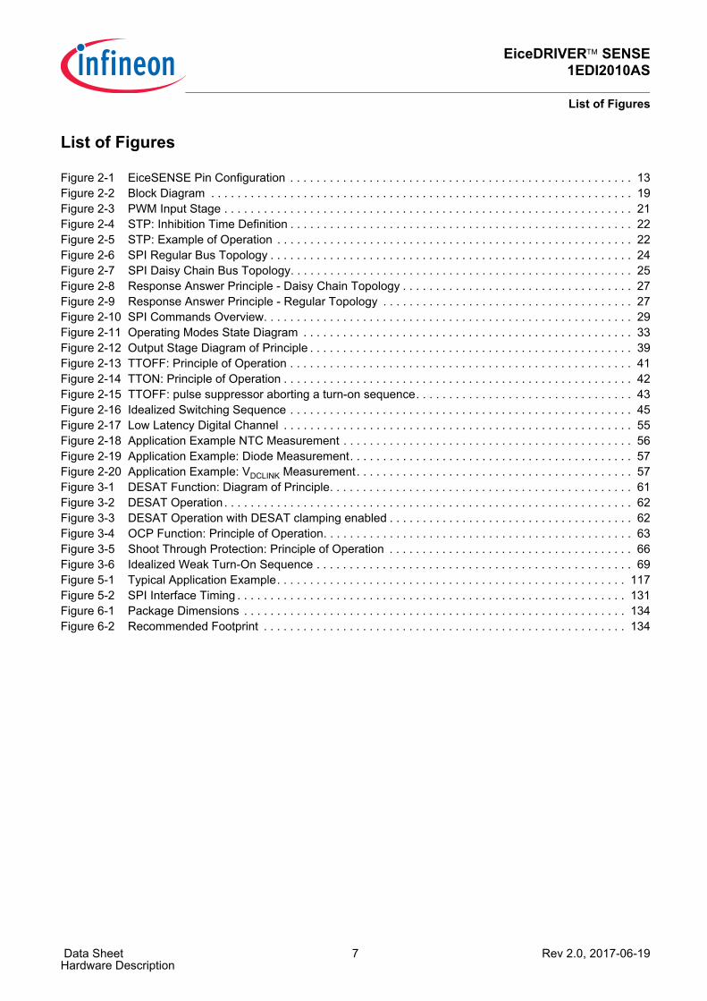
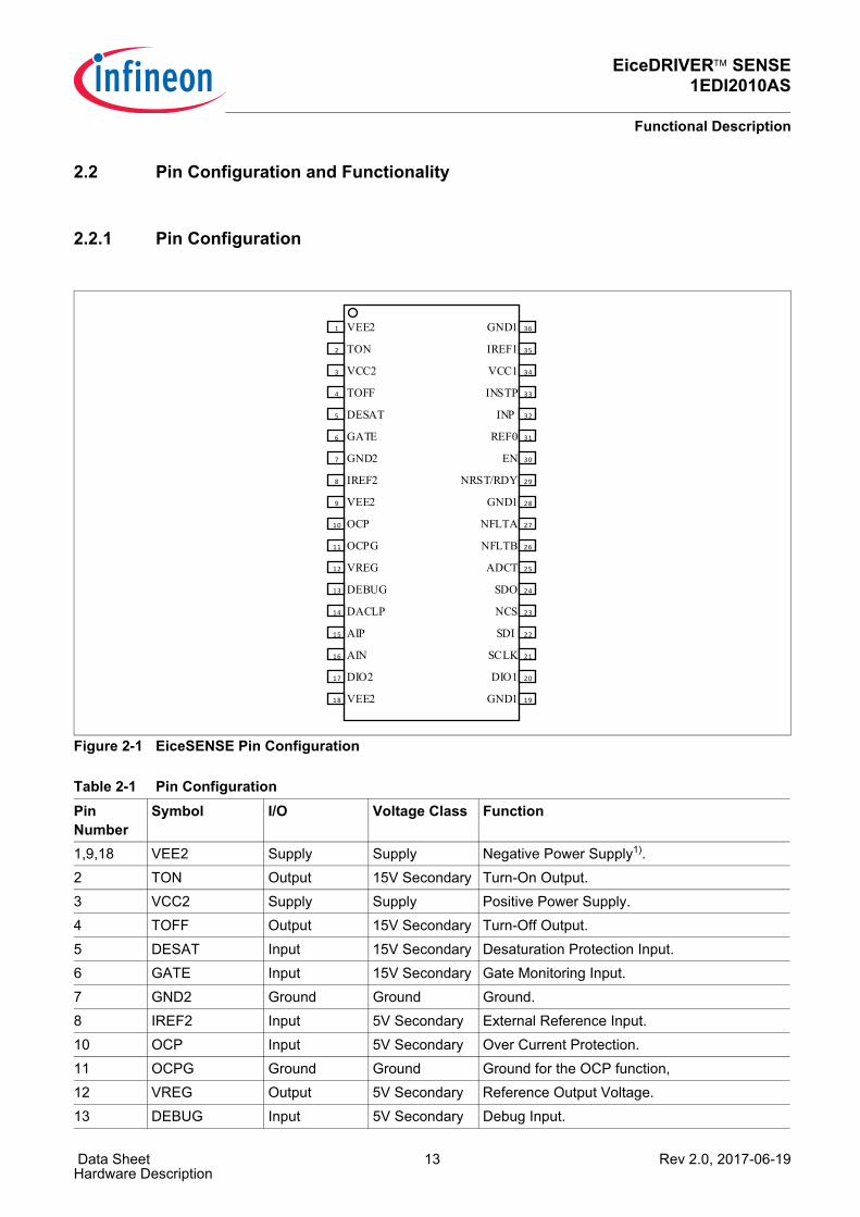
Figure 2-1 EiceSENSE Pin Configuration
Table 2-1 Pin ConfigurationPin Number
Symbol I/O Voltage Class Function
1,9,18 VEE2 Supply Supply Negative Power Supply1).2 TON Output 15V Secondary Turn-On Output.3 VCC2 Supply Supply Positive Power Supply.4 TOFF Output 15V Secondary Turn-Off Output.5 DESAT Input 15V Secondary Desaturation Protection Input.6 GATE Input 15V Secondary Gate Monitoring Input.7 GND2 Ground Ground Ground.8 IREF2 Input 5V Secondary External Reference Input.10 OCP Input 5V Secondary Over Current Protection.11 OCPG Ground Ground Ground for the OCP function,12 VREG Output 5V Secondary Reference Output Voltage.13 DEBUG Input 5V Secondary Debug Input.
OCPG
VREG
DESAT
IREF2
GND2
TOFF
VEE2
DIO2
GATE
DEBUG
VEE2
AIP
VCC2
DACLP
OCP
TON
VEE2 GND1
INSTP
EN
NRST/RDY
DIO1
SCLK
NFLTA
NCS
REF0
INP
IREF1
VCC1
GND11
2
3
4
5
6
7
8
9
10
11
12
13
14
15
16
17
18
36
35
34
33
32
31
30
25
24
23
22
21
20
19
NFLTB 26
SDI
27
GND1 28
SDO
29
ADCT
AIN
EiceDRIVER™ SENSE1EDI2010AS
Functional Description
Data Sheet 14 Rev 2.0, 2017-06-19Hardware Description
14 DACLP Output 5V Secondary Active Clamping Disable Output.15 AIP Input 5V Analog
SecondaryADC Positive Analog Input
16 AIN Input 5V Analog Secondary
ADC Negative Analog Input
17 DIO2 Input / Output 5V Secondary Digital I/O.
19, 28, 36 GND1 Ground Ground Ground2).20 DIO1 Input / Output 5V Primary Digital I/O.21 SCLK Input 5V Primary SPI Serial Clock Input.22 SDI Input 5V Primary SPI Serial Data Input.23 NCS Input 5V Primary SPI Chip Select Input (low active).24 SDO Output 5V Primary SPI Serial Data Output.25 ADCT Input 5V Primary ADC Trigger Input.26 NFLTB Output 5V Primary Fault B Output (low active, open drain).27 NFLTA Output 5V Primary Fault A Output (low active, open drain).29 NRST/RDY Input/Output 5V Primary Reset Input (low active, open drain). This signal
notifies that the device is “ready”.30 EN Input 5V Primary Enable Input.31 REF0 Ref. Ground Ground Reference Ground for signals INP, INSTP, EN.32 INP Input 5V Primary Positive PWM Input.33 INSTP Input 5V Primary Monitoring PWM Input.34 VCC1 Supply Input Supply Positive Power Supply.35 IREF1 Input 5V Primary External Reference Input.1) All VEE2 pins must be connected together.2) All GND1 pins must be connected together.
Table 2-1 Pin Configuration (cont’d)
Pin Number
Symbol I/O Voltage Class Function
EiceDRIVER™ SENSE1EDI2010AS
Functional Description
Data Sheet 15 Rev 2.0, 2017-06-19Hardware Description
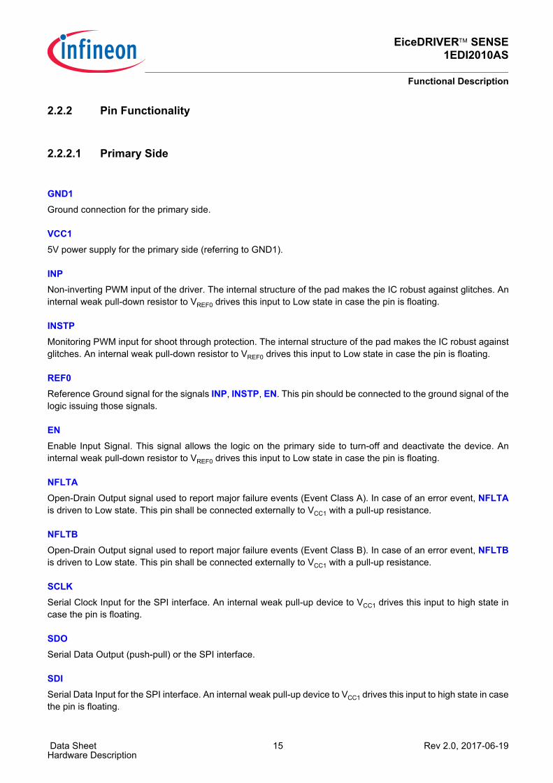
2.2.2 Pin Functionality
2.2.2.1 Primary Side
GND1Ground connection for the primary side.
VCC15V power supply for the primary side (referring to GND1).
INPNon-inverting PWM input of the driver. The internal structure of the pad makes the IC robust against glitches. Aninternal weak pull-down resistor to VREF0 drives this input to Low state in case the pin is floating.
INSTPMonitoring PWM input for shoot through protection. The internal structure of the pad makes the IC robust againstglitches. An internal weak pull-down resistor to VREF0 drives this input to Low state in case the pin is floating.
REF0Reference Ground signal for the signals INP, INSTP, EN. This pin should be connected to the ground signal of thelogic issuing those signals.
ENEnable Input Signal. This signal allows the logic on the primary side to turn-off and deactivate the device. Aninternal weak pull-down resistor to VREF0 drives this input to Low state in case the pin is floating.
NFLTAOpen-Drain Output signal used to report major failure events (Event Class A). In case of an error event, NFLTAis driven to Low state. This pin shall be connected externally to VCC1 with a pull-up resistance.
NFLTBOpen-Drain Output signal used to report major failure events (Event Class B). In case of an error event, NFLTBis driven to Low state. This pin shall be connected externally to VCC1 with a pull-up resistance.
SCLKSerial Clock Input for the SPI interface. An internal weak pull-up device to VCC1 drives this input to high state incase the pin is floating.
SDOSerial Data Output (push-pull) or the SPI interface.
SDISerial Data Input for the SPI interface. An internal weak pull-up device to VCC1 drives this input to high state in casethe pin is floating.

EiceDRIVER™ SENSE1EDI2010AS
Functional Description
Data Sheet 16 Rev 2.0, 2017-06-19Hardware Description
NCSChip Select input for the SPI interface. This signal is low active. An internal weak pull-up device to VCC1 drives thisinput to High state in case the pin is floating.
IREF1Reference input of the primary chip. This pin shall be connected to VGND1 via an external resistor.
NRST/RDYOpen drain reset input. This signal is low-active. When a valid signal is received on this pin, the device is broughtin its default state. This signal is also used as a “ready notification”. A high level on this pin indicates that theprimary chip is functional.
DIO1I/O for the digital channel. Depending of the chosen configuration of the device, this pin can be an input or anoutput (push-pull). An internal weak pull-down resistor to VGND1 drives this input to Low state in case the pin isfloating.
ADCTADC Trigger Input. An internal weak pull-down device to VGND1 drives this input to Low state in case the pin isfloating.
2.2.2.2 Secondary Side
VEE2Negative power supply for the secondary side, referring to VGND2.
VCC2Positive power supply for the secondary side, referring to VGND2.
GND2Reference ground for the secondary side.
DESATDesaturation Protection input pin. The function associated with this pin monitors the VCE voltage of the IGBT. Thedetection threshold is programmable. An internal pull-up resistor to VCC2 drives this signal to High level in case itis floating.
OCPOver Current Protection input pin. The function associated with this pin monitors the voltage across a sensingresistance located on the auxiliary path of a Current Sense IGBT. An internal weak pull-up resistor to the internal5V reference drives this input to High state in case the pin is floating.
OCPGOver Current Protection Ground.

EiceDRIVER™ SENSE1EDI2010AS
Functional Description
Data Sheet 17 Rev 2.0, 2017-06-19Hardware Description
TONOutput pin for turning on the IGBT.
TOFFOutput pin for turning off the IGBT.
GATEInput pin used to monitor the IGBT gate voltage.
DEBUGDebug input pin. This pin is latched at power-up. When a High level is detected on this pin, the device enters aspecial mode where it can be operated without SPI interface. This feature is for development purpose only. Thispin should normally be tied to VGND2. An internal weak pull-down resistor to VGND2 drives this input to Low state incase the pin is floating.
IREF2Reference input of the secondary chip. This pin shall be connected to VGND2 via an external resistor.
VREGReference Output voltage. This pin shall be connected to an external capacitance to VGND2.
DACLPOutput pin used to disable the active clamping function of the booster.
DIO2I/O for the digital channel. Depending of the chosen configuration of the device, this pin can be an input or anoutput (push-pull). An internal weak pull-down resistor to VGND2 drives this input to Low state in case the pin isfloating.
AIPADC positive analog input.
AINADC negative analog input.
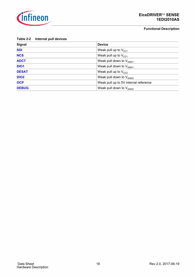
2.2.2.3 Pull DevicesSome of the pins are connected internally to pull-up or pull-down devices. This is summarized in Table 2-2.
Table 2-2 Internal pull devicesSignal DeviceINP Weak pull down to VREF0
INSTP Weak pull down to VREF0
EN Weak pull down to VREF0
SCLK Weak pull up to VCC1
EiceDRIVER™ SENSE1EDI2010AS
Functional Description
Data Sheet 18 Rev 2.0, 2017-06-19Hardware Description
SDI Weak pull up to VCC1
NCS Weak pull up to VCC1
ADCT Weak pull down to VGND1
DIO1 Weak pull down to VGND1
DESAT Weak pull up to VCC2
DIO2 Weak pull down to VGND2
OCP Weak pull up to 5V internal referenceDEBUG Weak pull down to VGND2
Table 2-2 Internal pull devicesSignal Device
EiceDRIVER™ SENSE1EDI2010AS
Functional Description
Data Sheet 19 Rev 2.0, 2017-06-19Hardware Description
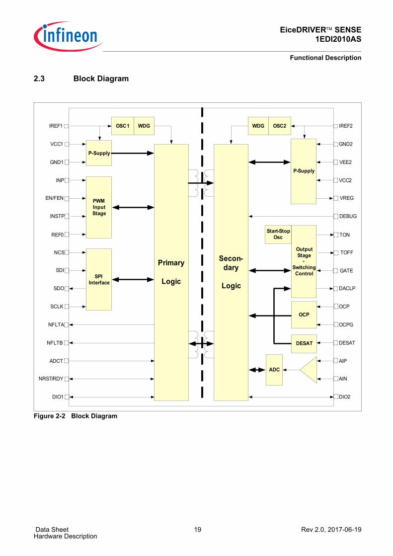
2.3 Block Diagram
Figure 2-2 Block Diagram
Primary
Logic
Secon-dary
Logic
VEE2
DESAT
Output Stage
-Switching Control
VCC2
DESAT
TON
OCP
GND1
VCC1
P-Supply
NFLTA
INP
INSTP
EN/FEN
NCS
SDI
SDO
SCLK
DEBUG
TOFF
NFLTB
OCP
PWMInputStage
SPIInterface
REF0
OSC1IREF1 OSC2 IREF2
GND2
Start-StopOsc
WDG WDG
NRST/RDY
VREG
OCPG
P-Supply
ADCAIPADCT
AIN
DACLP
DIO1 DIO2
GATE

EiceDRIVER™ SENSE1EDI2010AS
Functional Description
Data Sheet 20 Rev 2.0, 2017-06-19Hardware Description
2.4 Functional Block Description
2.4.1 Power SuppliesOn the primary side, the 1EDI2010AS needs a single 5 Vsupply source VCC1 for proper operation. This makes thedevice compatible to most of the microcontrollers available for automotive applications.On the secondary side, the 1EDI2010AS needs two power supplies for proper operation:• The positive power supply VCC2 is typically set to 15 V (referring to VGND2).• Optionally, a negative supply VEE2 (typically set to -8 V referring to VGND2) can be used. In case a negative
supply is not needed, VEE2 shall be connected to VGND2.Undervoltage monitoring on VCC1 and VCC2 is performed continuously during operation of the device (seeChapter 3.3.1). A 5V supply for the digital domain on the secondary side is generated internally (present at pin VREG).
2.4.2 Clock DomainsThe clock system of the 1EDI2010AS is based on three oscillators defining each a clock domain:• One RC oscillator (OSC1) for the primary chip.• One RC oscillator (OSC2) for the secondary chip excepting the output stage.• One Start-Stop oscillator (SSOSC2) for the output stage on the secondary side.The two RC oscillators are running constantly. They are also monitored constantly, and large deviations from thenominal frequency are identified as a system failure (Event Class B, see Chapter 2.4.9.2).The Start Stop oscillator is controlled by the PWM command.
EiceDRIVER™ SENSE1EDI2010AS
Functional Description
Data Sheet 21 Rev 2.0, 2017-06-19Hardware Description
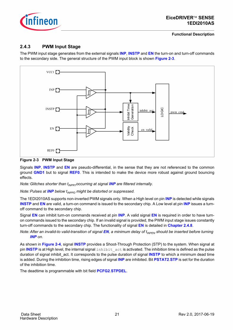
2.4.3 PWM Input StageThe PWM input stage generates from the external signals INP, INSTP and EN the turn-on and turn-off commandsto the secondary side. The general structure of the PWM input block is shown Figure 2-3.
Figure 2-3 PWM Input Stage
Signals INP, INSTP and EN are pseudo-differential, in the sense that they are not referenced to the commonground GND1 but to signal REF0. This is intended to make the device more robust against ground bouncingeffects.Note: Glitches shorter than tINPR1occurring at signal INP are filtered internally.
Note: Pulses at INP below tINPPD might be distorted or suppressed.
The 1EDI2010AS supports non-inverted PWM signals only. When a High level on pin INP is detected while signalsINSTP and EN are valid, a turn-on command is issued to the secondary chip. A Low level at pin INP issues a turn-off command to the secondary chip.Signal EN can inhibit turn-on commands received at pin INP. A valid signal EN is required in order to have turn-on commands issued to the secondary chip. If an invalid signal is provided, the PWM input stage issues constantlyturn-off commands to the secondary chip. The functionality of signal EN is detailed in Chapter 2.4.8.Note: After an invalid-to valid-transition of signal EN, a minimum delay of tINPEN should be inserted before turning
INP on.
As shown in Figure 2-4, signal INSTP provides a Shoot-Through Protection (STP) to the system. When signal atpin INSTP is at High level, the internal signal inhibit_act is activated. The inhibition time is defined as the pulseduration of signal inhibit_act. It corresponds to the pulse duration of signal INSTP to which a minimum dead timeis added. During the inhibition time, rising edges of signal INP are inhibited. Bit PSTAT2.STP is set for the durationof the inhibition time.The deadtime is programmable with bit field PCFG2.STPDEL.
REF0
LOG
IC
VCC1
INP
INSTP
EN
pwm_cmd
Valid
ity
Che
ck en_validIn
hibi
t Tim
e G
ener
atio
n
inhibit_act.
EiceDRIVER™ SENSE1EDI2010AS
Functional Description
Data Sheet 22 Rev 2.0, 2017-06-19Hardware Description
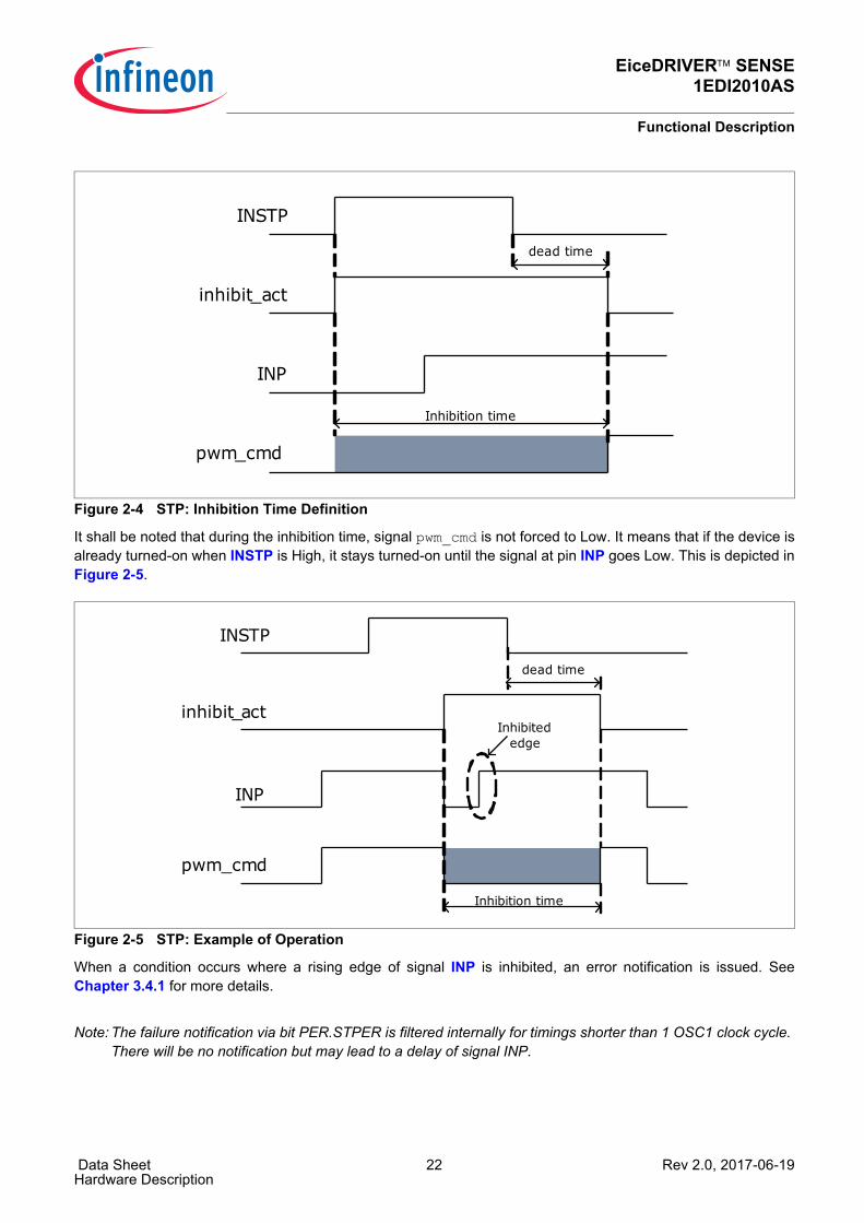
Figure 2-4 STP: Inhibition Time Definition
It shall be noted that during the inhibition time, signal pwm_cmd is not forced to Low. It means that if the device isalready turned-on when INSTP is High, it stays turned-on until the signal at pin INP goes Low. This is depicted inFigure 2-5.
Figure 2-5 STP: Example of Operation
When a condition occurs where a rising edge of signal INP is inhibited, an error notification is issued. SeeChapter 3.4.1 for more details.
Note: The failure notification via bit PER.STPER is filtered internally for timings shorter than 1 OSC1 clock cycle. There will be no notification but may lead to a delay of signal INP.
INSTP
INP
inhibit_act
pwm_cmd
dead time
Inhibition time
INSTP
INP
inhibit_act
pwm_cmd
Inhibition time
dead time
Inhibitededge

EiceDRIVER™ SENSE1EDI2010AS
Functional Description
Data Sheet 23 Rev 2.0, 2017-06-19Hardware Description
2.4.4 SPI InterfaceThis chapter describes the functionality of the SPI block.
2.4.4.1 OverviewThe standard SPI interface implemented on the 1EDI2010AS is compatible with most of the microcontrollersavailable for automotive and industrial applications. The following features are supported by the SPI interface:• Full-duplex bidirectional communication link.• SPI Slave mode (only).• 16-bit frame format.• Daisy chain capability.• MSB first.• Parity Check (optional) and Parity Bit generation (LSB).The SPI interface of the 1EDI2010AS provides a standardized bidirectional communication interface to the mainmicrocontroller. From the architectural point of view, it fulfills the following functions:• Initialization of the device.• Configuration of the device (static and runtime).• Reading of the status of the device (static and runtime).• Operation of the verification modes of the device.The purpose of the SPI interface is to exchange data which have relaxed timing constraints compared to the PWMsignals (from the point of view of the motor control algorithm). The IGBT switching behavior is for examplecontrolled directly by the PWM input. Similarly, critical application failures requiring fast reaction are notified on theprimary side via the feedback signals NFLTA, NFLTB and NRST/RDY.In order to minimize the complexity of the end-application and to optimize the microcontroller’s resources, theimplemented interface has daisy chain capability. Several (typically 6) 1EDI2010AS devices can be combined intoa single SPI bus.
EiceDRIVER™ SENSE1EDI2010AS
Functional Description
Data Sheet 24 Rev 2.0, 2017-06-19Hardware Description
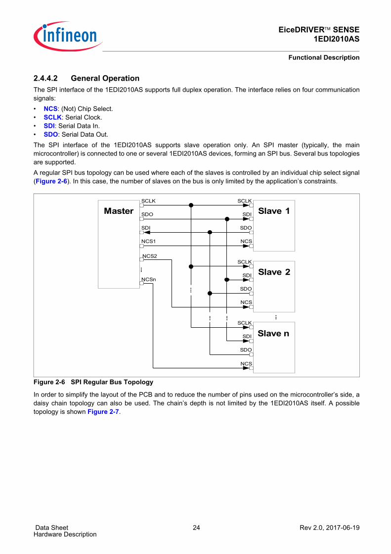
2.4.4.2 General OperationThe SPI interface of the 1EDI2010AS supports full duplex operation. The interface relies on four communicationsignals:• NCS: (Not) Chip Select.• SCLK: Serial Clock.• SDI: Serial Data In.• SDO: Serial Data Out.The SPI interface of the 1EDI2010AS supports slave operation only. An SPI master (typically, the mainmicrocontroller) is connected to one or several 1EDI2010AS devices, forming an SPI bus. Several bus topologiesare supported.A regular SPI bus topology can be used where each of the slaves is controlled by an individual chip select signal(Figure 2-6). In this case, the number of slaves on the bus is only limited by the application’s constraints.
Figure 2-6 SPI Regular Bus Topology
In order to simplify the layout of the PCB and to reduce the number of pins used on the microcontroller’s side, adaisy chain topology can also be used. The chain’s depth is not limited by the 1EDI2010AS itself. A possibletopology is shown Figure 2-7.
SCLK
Master SDO
SDI
NCS1
SCLK
SDI
SDO
NCS
Slave 1
SCLK
SDI
SDO
NCS
Slave 2
SCLK
SDI
SDO
NCS
Slave n
...
...
...
NCSn
...
...
NCS2
EiceDRIVER™ SENSE1EDI2010AS
Functional Description
Data Sheet 25 Rev 2.0, 2017-06-19Hardware Description
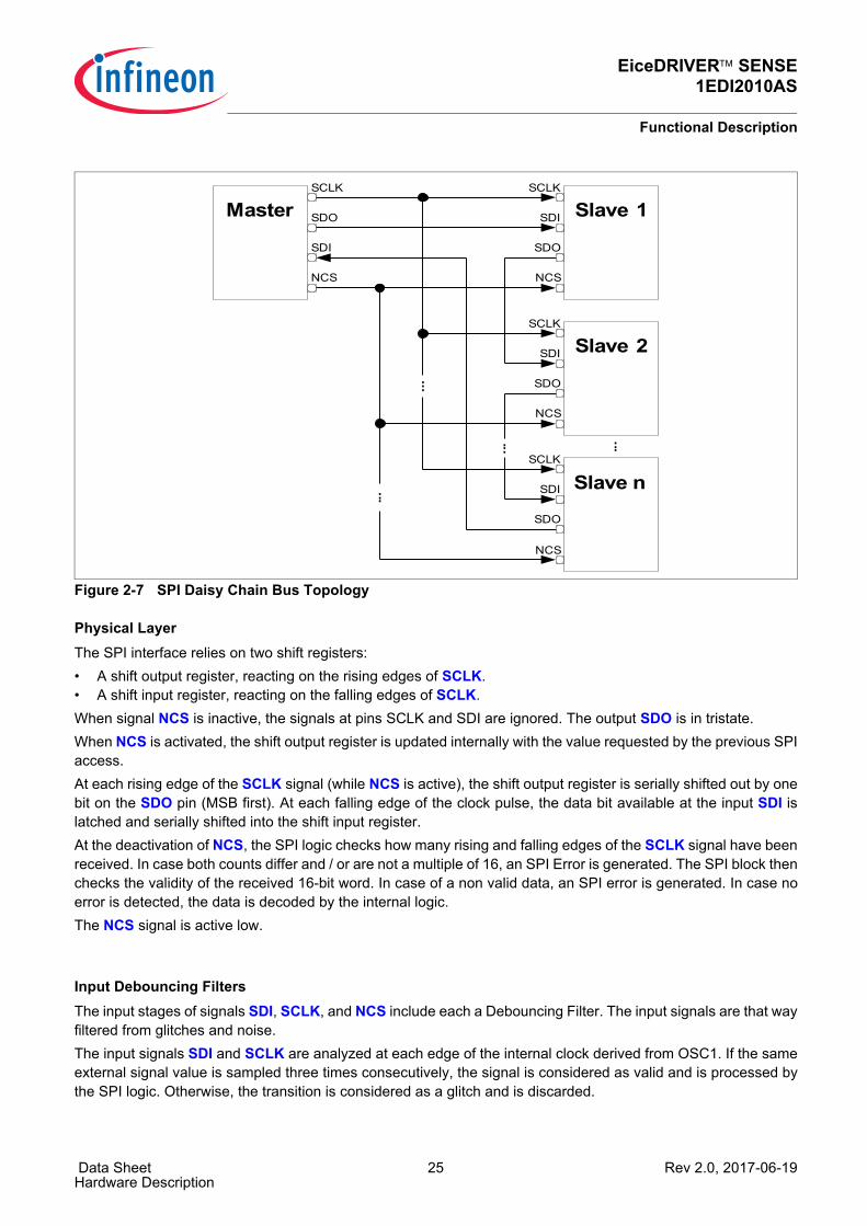
Figure 2-7 SPI Daisy Chain Bus Topology
Physical LayerThe SPI interface relies on two shift registers:• A shift output register, reacting on the rising edges of SCLK.• A shift input register, reacting on the falling edges of SCLK.When signal NCS is inactive, the signals at pins SCLK and SDI are ignored. The output SDO is in tristate.When NCS is activated, the shift output register is updated internally with the value requested by the previous SPIaccess.At each rising edge of the SCLK signal (while NCS is active), the shift output register is serially shifted out by onebit on the SDO pin (MSB first). At each falling edge of the clock pulse, the data bit available at the input SDI islatched and serially shifted into the shift input register.At the deactivation of NCS, the SPI logic checks how many rising and falling edges of the SCLK signal have beenreceived. In case both counts differ and / or are not a multiple of 16, an SPI Error is generated. The SPI block thenchecks the validity of the received 16-bit word. In case of a non valid data, an SPI error is generated. In case noerror is detected, the data is decoded by the internal logic.The NCS signal is active low.
Input Debouncing FiltersThe input stages of signals SDI, SCLK, and NCS include each a Debouncing Filter. The input signals are that wayfiltered from glitches and noise.The input signals SDI and SCLK are analyzed at each edge of the internal clock derived from OSC1. If the sameexternal signal value is sampled three times consecutively, the signal is considered as valid and is processed bythe SPI logic. Otherwise, the transition is considered as a glitch and is discarded.
SCLK
Master SDO
SDI
NCS
SCLK
SDI
SDO
NCS
Slave 1
SCLK
SDI
SDO
NCS
Slave 2
SCLK
SDI
SDO
NCS
Slave n
...
...
...
...
EiceDRIVER™ SENSE1EDI2010AS
Functional Description
Data Sheet 26 Rev 2.0, 2017-06-19Hardware Description
The input signal NCS is sampled at a rate corresponding to the period of the internal clock derived from OSC1. Ifthe same external signal value is sampled two times consecutively, the signal is considered as valid and isprocessed by the SPI logic. Otherwise, the transition is considered as a glitch and is discarded.
2.4.4.3 Definitions
CommandA command is a high-level command issued by the SPI master which aims at generating a specific reaction in theaddressed slave. The command is physically translated into a Request Message by the SPI master. The correctreception of the Request Message by the SPI slave leads to a specific action inside the slave and to the emissionof an Answer Message by the slave.Example: the READ command leads to the transfer of the value of the specified register from the device to the SPImaster.
WordA word is a 16-bit sequence of shifted data bits.
TransferA transfer is defined as the SPI data transfers (in both directions) occurring between a falling edge of NCS andthe next consecutive rising edge of NCS.
Request MessageA request message is a word issued by the SPI master and addressing a single slave. A request message relatesto a specific command.
Answer MessageAn answer message is a well-defined word issued by a single SPI slave as a response to a request message.
Transmit FrameA transmit frame is a sequence of one or several words sent by the SPI Master within one SPI transfer. In regularSPI topologies, a transmit frame is in practice identical to a data word. In daisy chain topologies, a transmit frameis a sequence of data words belonging to different request messages.
Receive FrameA receive frame is a sequence of one or several words received by the SPI Master within one SPI transfer. Inregular SPI topologies, a receive frame is in practice identical to a data word. In daisy chain topologies, a receiveframe is a sequence of data words belonging to different Answer Messages.
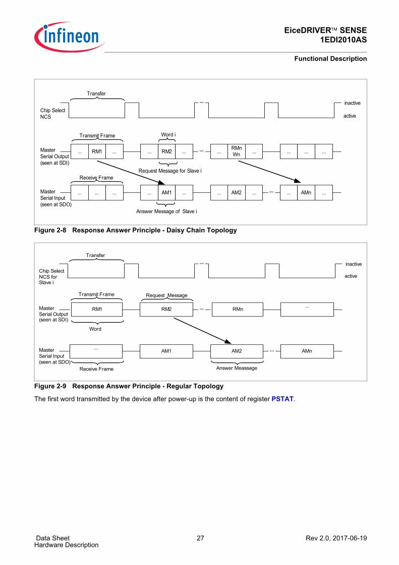
The SPI protocol supported by the 1EDI2010AS is based on the Request / Answer principle. The master sends adefined request message to which the slave answers with the corresponding answer message (Figure 2-8,Figure 2-9). Due to the nature of the SPI interface, the Answer Message is shifted, compared to the RequestMessage, by one SPI transfer. It means, for example, that the last word of answer message n is transmitted bythe slave while the master sends the first word of request message n+1.
EiceDRIVER™ SENSE1EDI2010AS
Functional Description
Data Sheet 27 Rev 2.0, 2017-06-19Hardware Description
Figure 2-8 Response Answer Principle - Daisy Chain Topology
Figure 2-9 Response Answer Principle - Regular Topology
The first word transmitted by the device after power-up is the content of register PSTAT.
Chip Select NCS
MasterSerial Output(seen at SDI)
... RM1 ... RM2 ...
AM1 ... ... ... ...
Transfer
Transmit Frame
Receive Frame
MasterSerial Input(seen at SDO)
...
RMnWn... ...
AM2... ...
... ... ... ...
... ... AMn
Word i
Answer Message of Slave i
...
...
inactive
active
Request Message for Slave i
...
Chip Select NCS for Slave i
MasterSerial Output(seen at SDI)
RM1
AM1...
Transfer
Transmit Frame
Receive Frame
MasterSerial Input(seen at SDO)
...
AM2
... ...
AMn
inactive
active
RM2 RMn
Word
...
Answer Meassage
Request Message

EiceDRIVER™ SENSE1EDI2010AS
Functional Description
Data Sheet 28 Rev 2.0, 2017-06-19Hardware Description
2.4.4.4 SPI Data Integrity Support
2.4.4.4.1 Parity BitBy default, the SPI link relies on an odd parity protection scheme for each transmitted or received 16-bit word ofthe SPI message. The parity bit corresponds to the LSB of the 16-bit word. Therefore, the effective payload of a16-bit word is 15 data bit (plus one parity bit). The parity bit check (on the received data) can be disabled byclearing bit PCFG.PAREN. In this case, the parity bit is considered as “don’t care”. The generation of the parity bitby the driver for transmitted words can not be disabled (but can be considered as “don’t care” by the SPI master).Note: For fixed value commands (ENTER_CMODE, ENTER_VMODE, EXIT_CMODE, NOP), it has to be ensured
that the value of the parity bit is correct even if parity check is disabled. Otherwise, an SPI error will be generated.
2.4.4.4.2 SPI ErrorWhen the device is not able to process an incoming request message, an SPI error is generated: the receivedmessage is discarded by the driver, bit PER.SPIERis set and the erroneous message is answered with an errornotification (bit LMI set).Several failures generate an SPI error:• A parity error is detected on the received word.• An invalid data word format is received (e.g. not a 16 bit word).• A word is received, which does not corresponding to a valid Request Message.• A command is received which can not be processed. For example, the driver receives in Active Mode a
command which is only valid in other operating modes. Another typical example is a read access to the secondary while the previous read access is not yet completed (device “busy”).
• An SPI access to an invalid address.
EiceDRIVER™ SENSE1EDI2010AS
Functional Description
Data Sheet 29 Rev 2.0, 2017-06-19Hardware Description
2.4.4.5 Protocol Description
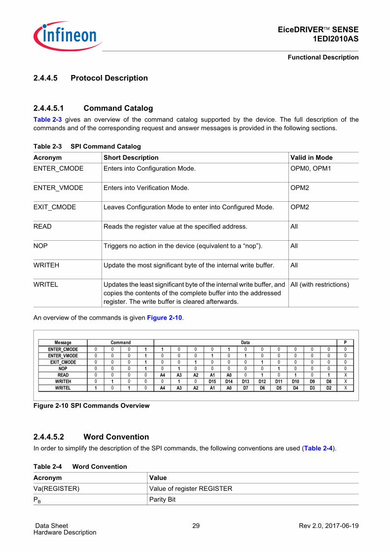
2.4.4.5.1 Command CatalogTable 2-3 gives an overview of the command catalog supported by the device. The full description of thecommands and of the corresponding request and answer messages is provided in the following sections.
An overview of the commands is given Figure 2-10.
Figure 2-10 SPI Commands Overview
2.4.4.5.2 Word ConventionIn order to simplify the description of the SPI commands, the following conventions are used (Table 2-4).
Table 2-3 SPI Command CatalogAcronym Short Description Valid in ModeENTER_CMODE Enters into Configuration Mode. OPM0, OPM1
ENTER_VMODE Enters into Verification Mode. OPM2
EXIT_CMODE Leaves Configuration Mode to enter into Configured Mode. OPM2
READ Reads the register value at the specified address. All
NOP Triggers no action in the device (equivalent to a “nop”). All
WRITEH Update the most significant byte of the internal write buffer. All
WRITEL Updates the least significant byte of the internal write buffer, and copies the contents of the complete buffer into the addressed register. The write buffer is cleared afterwards.
All (with restrictions)
Table 2-4 Word ConventionAcronym ValueVa(REGISTER) Value of register REGISTERPB Parity Bit
Message PENTER_CMODE 0 0 0 1 1 0 0 0 1 0 0 0 0 0 0 0ENTER_VMODE 0 0 0 1 0 0 0 1 0 1 0 0 0 0 0 0EXIT_CMODE 0 0 0 1 0 0 1 0 0 0 1 0 0 0 0 0
NOP 0 0 0 1 0 1 0 0 0 0 0 1 0 0 0 0READ 0 0 0 0 A4 A3 A2 A1 A0 0 1 0 1 0 1 X
WRITEH 0 1 0 0 0 1 0 D15 D14 D13 D12 D11 D10 D9 D8 XWRITEL 1 0 1 0 A4 A3 A2 A1 A0 D7 D6 D5 D4 D3 D2 X
DataCommand
EiceDRIVER™ SENSE1EDI2010AS
Functional Description
Data Sheet 30 Rev 2.0, 2017-06-19Hardware Description
2.4.4.5.3 ENTER_CMODE CommandThe goal of this function is to set the device into Configuration Mode. After reception of a valid ENTER_CMODEcommand, mode OPM2 is active. This command is only valid in Default Mode (OPM0 and OPM1). In case therequest message is received while OPM1 is not active, the complete command is discarded and an SPI erroroccurs.Table 2-5 describes the request message and the corresponding answer message.
2.4.4.5.4 ENTER_VMODE CommandThe goal of this function is to set the device into Verification Mode. After reception of a valid ENTER_VMODEcommand, mode OPM5 is active. This command is only valid in Configuration Mode (OPM2). In case the requestmessage is received while OPM2 is not active, the complete command is discarded and an SPI error occurs.Table 2-6 describes the request message and the corresponding answer message.
2.4.4.5.5 EXIT_CMODE CommandWhen a valid EXIT_CMODE is received by the device, the Configuration Mode is left to Configured Mode (ModeOPM3 active). This command is only valid in Configuration Mode (OPM2). In case the request message isreceived while OPM2 is not active, the complete command is discardedand an SPI error occurs.Table 2-7 describes the request message and the corresponding answer message.
<<n Left shift operation of n bits.xH | yH Result of the operation: xH OR yH
Table 2-5 ENTER_CMODE request and answer messagesTransfer 1 Transfer 2
Request message 1880H N.a.Answer message N.a. Va(PSTAT)
Table 2-6 ENTER_VMODE request and answer messagesTransfer 1 Transfer 2
Request message 1140H N.a.Answer message N.a. Va(PSTAT)
Table 2-7 EXIT_CMODE request and answer messagesTransfer 1 Transfer 2
Request message 1220H N.a.Answer message N.a. Va(PSTAT)
Table 2-4 Word Convention (cont’d)
Acronym Value
EiceDRIVER™ SENSE1EDI2010AS
Functional Description
Data Sheet 31 Rev 2.0, 2017-06-19Hardware Description
2.4.4.5.6 NOP CommandThis command triggers no specific action in the driver (equivalent to a “nop”). However, the mechanisms verifyingthe validity of the word are active. This command is valid in all operating modes.Table 2-8 describes the request message and the corresponding answer message.
2.4.4.5.7 READ CommandThis command aims at reading the value of the register whose address is specified in the request message. Thiscommand is valid in all operating modes. However, in OPM4 and OPM6, the use of the READ command isrestricted (see Table 4-4). If an access outside the allowed address range is performed, the access is discardedas invalid and an SPI error occurs.Table 2-9 describes the request message and the corresponding answer message.
Request message wordsWord 1: ( ADDRESS_5BIT << 7 )] | 002AH | PB.
Answer message wordsWord 1: Value of REGISTER.
2.4.4.5.8 WRITEHThis command aims at writing the upper byte of the internal write buffer with the specified value. This commandhas no other effect on the functionality of the device. This command is valid in all operating modes.Table 2-10 describes the request message and the corresponding answer message.
Request message wordsWord 1: 4400H | ( DATA_8BIT << 1 ) | PB
Table 2-8 NOP request and answer messagesTransfer 1 Transfer 2
Request message 1410H N.a.Answer message N.a. Va(PSTAT)
Table 2-9 READ request and answer messagesTransfer 1 Transfer 2
Request message See below N.a.Answer message N.a. Va(Register)
Table 2-10 WRITEH request and answer messagesTransfer 1 Transfer 2
Request message See below N.a.Answer message N.a. Va(PSTAT)
EiceDRIVER™ SENSE1EDI2010AS
Functional Description
Data Sheet 32 Rev 2.0, 2017-06-19Hardware Description
2.4.4.5.9 WRITELThis command aims at updating the value of the register whose address is specified in the request message. Thiscommand is valid in all operating modes. However, depending on the active operating mode, this command isrestricted to a given address range or specific registers (see Table 4-5). If an access outside the allowed addressrange is performed, the access is discarded as invalid and an SPI error occurs.At the reception of this command, the least significant byte of the internal buffer is written with the specified value,the contents of the buffer is copied to the register at the specified address and the complete write buffer is cleared.Table 2-11 describes the request message and the corresponding answer message.
Request message wordsWord 1: A000H | ( ADDRESS_5BIT << 7 ) | ( DATA_6BIT << 1 ) | PB.
Table 2-11 WRITEL request and answer messagesTransfer 1 Transfer 2
Request message See below N.a.Answer message N.a. Va(PSTAT)
EiceDRIVER™ SENSE1EDI2010AS
Functional Description
Data Sheet 33 Rev 2.0, 2017-06-19Hardware Description
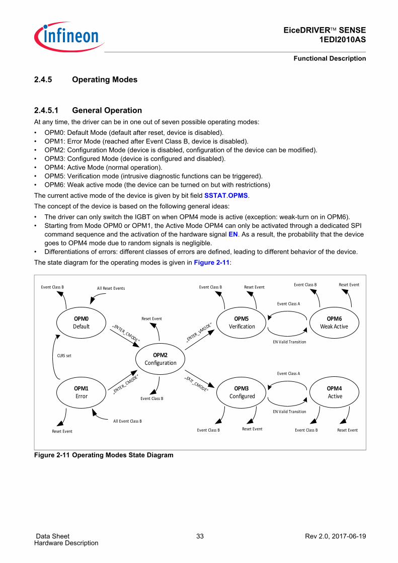
2.4.5 Operating Modes
2.4.5.1 General OperationAt any time, the driver can be in one out of seven possible operating modes:• OPM0: Default Mode (default after reset, device is disabled).• OPM1: Error Mode (reached after Event Class B, device is disabled).• OPM2: Configuration Mode (device is disabled, configuration of the device can be modified).• OPM3: Configured Mode (device is configured and disabled).• OPM4: Active Mode (normal operation).• OPM5: Verification mode (intrusive diagnostic functions can be triggered).• OPM6: Weak active mode (the device can be turned on but with restrictions)The current active mode of the device is given by bit field SSTAT.OPMS.The concept of the device is based on the following general ideas:• The driver can only switch the IGBT on when OPM4 mode is active (exception: weak-turn on in OPM6).• Starting from Mode OPM0 or OPM1, the Active Mode OPM4 can only be activated through a dedicated SPI
command sequence and the activation of the hardware signal EN. As a result, the probability that the device goes to OPM4 mode due to random signals is negligible.
• Differentiations of errors: different classes of errors are defined, leading to different behavior of the device.The state diagram for the operating modes is given in Figure 2-11:
Figure 2-11 Operating Modes State Diagram
OPM0Default
Event Class B
OPM5Verification
OPM4Active
„ENTER_VMODE“
Reset Event
Event Class A
All Reset Events
EN Valid Transition
OPM2Configuration
OPM3Configured
OPM6Weak Active
Event Class A
EN Valid Transition
„EXIT_CMODE“OPM1Error
„ENTER_CMODE“
„ENTER_CMODE“
Event Class B Reset Event
Event Class B Reset Event Event Class B Reset Event
All Event Class B
Event Class B
CLRS set
Reset Event
Event Class B
Reset Event
EiceDRIVER™ SENSE1EDI2010AS
Functional Description
Data Sheet 34 Rev 2.0, 2017-06-19Hardware Description
2.4.5.2 Definitions
2.4.5.2.1 Events and State TransitionsThe transitions from one state to the other are based on “events” and / or SPI commands. The followingclassification is chosen for defining the events.
Events Class AThe following (exhaustive) list of events are defined as Events Class A: • Occurrence of a DESAT event (leads to a safe turn-off sequence).• Occurrence of an OCP event (leads to a safe turn-off sequence).• Valid to Invalid transition on EN signal (leads to a regular turn-off sequence).• ADC Boundary Check Violation Event (optional, can be disabled).When an Event Class A occurs, the output stage either initiates either a safe turn-off sequence (DESAT, OCP) ora regular turn-off sequence (all other events).The event is notified via an error bit in the corresponding register.Note: Contrarily to a reset event, an Event Class A does not affect the contents of the configuration registers.
When an Event Class A occurs, the device may change its operating mode depending on which mode is activewhen the event occurs:• If it was in OPM4, it goes in OPM3.• If it was in OPM6, it goes in OPM5.In all other cases, the OPM is unaffected. A state transition due to an Event Class A leads to the activation of signalNFLTA. If no state transition occurs (if for example the device was not in OPM4 or OPM6), NFLTA is not activated(exception: ADC Boundary Check event - see Chapter 2.4.7 for more details on failure notifications).
Events Class BThe following (exhaustive) list of events are defined as Events Class B: • Occurrence of a UVLO2 event.• Verification Mode Time Out ErrorWhen an Event Class B occurs, the output stage initiates a regular turn-off sequence. The event is notified via anerror bit in the corresponding register and (possibly) via the signal NFLTB.Note: Events Class B may affect the contents of the configuration registers.
When an Event Class B occurs, the device may change its operating mode depending on which mode is activewhen the event occurs: if it was not in OPM1, it goes to OPM1. It is unaffected otherwiseA state transition due to an Event Class B leads to the activation of signal NFLTB. If no state transition occurs (iffor example the device was already in OPM1), NFLTB is not activated. See Chapter 2.4.7 for more details onfailure notifications.
Events Class CGenerally speaking, Events Class C are error events that do not lead to a change of the operating mode of thedevice. The following (non-exhaustive) list of events is comprised within the Event Class C:• SPI Error.• Shoot Through Protection error.• Etc.
EiceDRIVER™ SENSE1EDI2010AS
Functional Description
Data Sheet 35 Rev 2.0, 2017-06-19Hardware Description
SPI CommandsThe following SPI commands have an impact on the device’s operating mode. The SPI commands are describedin Chapter 2.4.4.5.• ENTER_CMODE.• ENTER_VMODE.• EXIT_CMODE.• Setting of bit SCTRL.CLRS (by writing register PCTRL)
Reset EventsA reset sets the device (or part of the device) in its default state. Reset events are described in Chapter 2.4.10.Internal Supervision Error are leading to a reset event, for example.
2.4.5.2.2 Emergency Turn-Off SequenceThe denomination “Emergency Turn-Off Sequence” (ETO) is used to describe the sequence of actions executedby the output stage of the device when an Event Class A, Class B or a Reset Event is detected.An ETO sequence is described by the following set of actions:• A Turn-Off sequence is initiated. In case of DESAT or OCP event, a safe turn-off sequence is initiated. For the
other events, a regular turn-off sequence is initiated.• The device enters the corresponding OPM mode. As a consequence, the device is disabled.Once an ETO has been initiated, the device can not be reenabled for a maximum duration consisting of 256 OSC2clock cycles. Consequently, the user shall wait for this duration before reenabling the device and sending PWMturn-on command.
2.4.5.2.3 Ready, Disabled, Enabled and Active StateThe device is said to be in Ready state in case no reset event is active on the primary chip. When the device isReady, signal NRST/RDY is at High level.When the device is in Disabled State, the PWM turn-on commands are ignored. This means that whatever theinput signal INP is, the output stage (if not tristated) delivers a constant turn-off signal to the IGBT. Unlessotherwise stated, all other functions of the device work normally.When the device is not in Disabled State, it is said to be in Enabled State. In this case, the PWM signal commandis processed normally (if the output stage is not tristated). Practically, the device is in Enabled State when eitherMode OPM4 or Mode OPM6 is active.Active State corresponds to the normal operating state of the device. Practically, the device is in Active State whenMode OPM4 is active.Note: When the device is in Active State, it implicates it is in Enabled state.
EiceDRIVER™ SENSE1EDI2010AS
Functional Description
Data Sheet 36 Rev 2.0, 2017-06-19Hardware Description
2.4.5.3 Operation Modes Description
Default Mode (OPM0)Mode OPM0 is the default operating mode of the device after power up or after a rest event. In OPM0, the deviceis in Disabled State.The following exhaustive list of events bring the device in OPM0 Mode:• Occurrence of a Reset Event.• Bit SCTRL.CLRS set while the device was in OPM1.
Error Mode (OPM1) Mode OPM1 is the operating mode of the device after an Event Class B.The following exhaustive list of events bring the device in OPM1 Mode:• Occurrence of an Event Class B.In OPM1, when bit SCTRL.CLRS is set via the corresponding SPI command, the device shall normally jump toOPM0. However, in case the conditions for an Event Class B are met at that moment, no state transition occursand the device stays in OPM1. The operation of bit SCTRL.CLRS on the secondary sticky bits works normally.In OPM1, when a valid ENTER_CMODE command is received, the device shall normally jump to OPM2.However, in case the conditions for an Event Class B are met at that moment, no state transition occurs and thedevice stays in OPM1 for the duration of the event. The state transition to OPM2 is executed as soon as theconditions leading to the Event Class B disappear.It shall be noted that no LMI error notification is issued.
Configuration Mode (OPM2)Configuration Mode is the mode where the configuration of the device can be modified. When OPM2 is active, thedevice is in Disabled State.The following exhaustive list of events bring the device in Configuration Mode:• Reception of a valid ENTER_CMODE command while Mode OPM0 or OPM1 active.
Configured Mode (OPM3)Configured Mode is the mode where the device is ready to be enabled. When OPM3 is active, the device is inDisabled State.The following exhaustive list of events bring the device in Mode OPM3:• Reception of a valid EXIT_CMODE command while Mode OPM2 active.• Event Class A while Mode OPM4 active.
Active Mode (OPM4)The Active Mode corresponds to the normal operating mode of the device. When OPM4 is active, the device is inActive State. The following exhaustive list of event bring the device in Active Mode:• Invalid to Valid Transition on signal EN while Mode OPM3 active.

EiceDRIVER™ SENSE1EDI2010AS
Functional Description
Data Sheet 37 Rev 2.0, 2017-06-19Hardware Description
Verification Mode (OPM5)Verification Mode is the mode where intrusive verification functions can be started. When OPM5 is active, thedevice is in disabled state.The following exhaustive list of event bring the device in Verification Mode:• Reception of a valid ENTER_VMODE command while Mode OPM2 active.• Occurrence of an Event Class A while Mode OPM6 active.After a transition from Mode OPM2 to OPM5, an internal watchdog timer is started. If after time tVMTO, the devicehas not left both modes OPM5 or OPM6, a time-out event occurs and an Event Class B is generated.
Weak Active Mode (OPM6)Weak Active Mode is the mode where the device can be activated to run diagnosis tests at system level. WhenOPM6 is active, the device is in Enabled State. A PWM turn-on command issues a Weak Turn-On on thesecondary side.The following exhaustive list of event bring the device in Weak Active Mode:• Invalid to Valid Transition on signal EN while Mode OPM5 active.The watchdog counter started when entering Mode OPM5 is not reset when entering OPM6.
Implementation Notes related to State Transitions• An Event Class A or Class B detected on the secondary side lead to an immediate reaction of the device’s
output stage. Due to the latency of the inter-chip communication, the notification on the primary side is slightly delayed.
• The activation of signal NFLTA or NFLTB is simultaneous to the corresponding state transition on the primary side.
• It is possible to change the operating mode while a failure condition is present. This may however lead to a new immediate error notification and state transition.
2.4.5.4 Activating the device after resetAfter a reset event, the device is in Mode OPM0 and disabled. In order to be active, the device needs to enterConfiguration Mode with the ENTER_CMODE command. Once all the configurations have been performed, theConfiguration Mode has to be exited with an EXIT_CMODE command. Once this is done, the device can enterthe Active Mode when Invalid to Valid transition on pin EN is detected.
2.4.5.5 Activating the device after an Event Class A or BIf during operation, an Event Class A occurs, the device enters the OPM3 (or OPM5). Bit field SSTAT.OPMS isupdated accordingly. In order to reactivate the device, an invalid-to-valid transition has to be applied to signal EN.It means for example in EN Mode, that a Low-level and then a High level is applied to EN. If no Event Class Aevent is active, the device will enter OPM4 (respectively OPM6).If during operation, an Event Class B occurs, the device enters the Default Mode OPM1. Bit field SSTAT.OPMSis updated accordingly. In order to reactivate the device, the steps defined in Chapter 2.4.5.4 need to beperformed.

EiceDRIVER™ SENSE1EDI2010AS
Functional Description
Data Sheet 38 Rev 2.0, 2017-06-19Hardware Description
2.4.5.6 Debug ModeThe DEBUG pin gives the possibility to operate the device in the so-called Debug Mode. The goal of the DebugMode is to operate the device without SPI interface. This mode should be used for development purpose only andis not intended to be used in final applications.At VCC2 power-on, the level at pin DEBUG is latched. In case a High level is detected, the device enters the DebugMode. Bit SSTAT.DBG is then set.In Debug Mode, the regular operation of the internal state machine is modified, so that the device can only enterOPM3 or OPM4. As a result Modes OPM0, OPM1, OPM2, OPM5 and OPM6 are completely bypassed. In caseof a Reset event, the device goes to OPM3 (instead of OPM0). Besides, in Debug Mode, events leading normallyto an Event Class B are replaced an Event Class A, resulting in the activation of signal NFLTA. Event Class B aretherefore not generated by the device in Debug Mode (and signal NFLTB shall not be used).It should be noted that the configuration of the device in Debug Mode corresponds to the default settings and cannot be changed.In Debug Mode, the operation of the device is otherwise similar to regular operation. It means in particular that thesignal EN has to be managed properly: when the device is in OPM3, a Low to High level transition has to beapplied to the device in order to enter OPM4 (Active Mode).Note: Once it has been latched at power-on, the level on the pin DEBUG has no impact on the device until the next
power-on event on the secondary side.
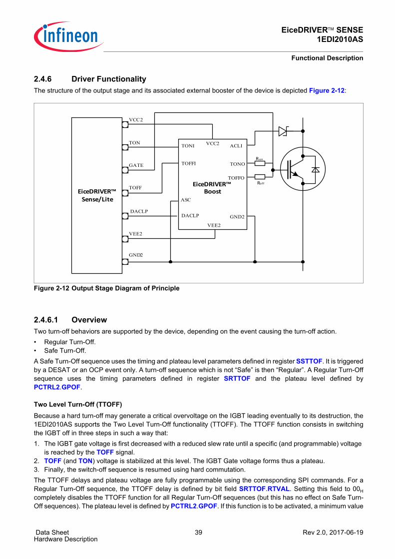
EiceDRIVER™ SENSE1EDI2010AS
Functional Description
Data Sheet 39 Rev 2.0, 2017-06-19Hardware Description
2.4.6 Driver FunctionalityThe structure of the output stage and its associated external booster of the device is depicted Figure 2-12:
Figure 2-12 Output Stage Diagram of Principle
2.4.6.1 OverviewTwo turn-off behaviors are supported by the device, depending on the event causing the turn-off action.• Regular Turn-Off.• Safe Turn-Off.A Safe Turn-Off sequence uses the timing and plateau level parameters defined in register SSTTOF. It is triggeredby a DESAT or an OCP event only. A turn-off sequence which is not “Safe” is then “Regular”. A Regular Turn-Offsequence uses the timing parameters defined in register SRTTOF and the plateau level defined byPCTRL2.GPOF.
Two Level Turn-Off (TTOFF)Because a hard turn-off may generate a critical overvoltage on the IGBT leading eventually to its destruction, the1EDI2010AS supports the Two Level Turn-Off functionality (TTOFF). The TTOFF function consists in switchingthe IGBT off in three steps in such a way that:1. The IGBT gate voltage is first decreased with a reduced slew rate until a specific (and programmable) voltage
is reached by the TOFF signal.2. TOFF (and TON) voltage is stabilized at this level. The IGBT Gate voltage forms thus a plateau.3. Finally, the switch-off sequence is resumed using hard commutation.The TTOFF delays and plateau voltage are fully programmable using the corresponding SPI commands. For aRegular Turn-Off sequence, the TTOFF delay is defined by bit field SRTTOF.RTVAL. Setting this field to 00Hcompletely disables the TTOFF function for all Regular Turn-Off sequences (but this has no effect on Safe Turn-Off sequences). The plateau level is defined by PCTRL2.GPOF. If this function is to be activated, a minimum value
EiceDRIVER™ Sense/Lite
VCC2
TOFF
DACLP
TON
GATERon
Roff
VEE2
GND2
TONI
TONO
TOFFO
ACLI
TOFFI
DACLP
ASC
EiceDRIVER™ Boost
VCC2
GND2
VEE2

EiceDRIVER™ SENSE1EDI2010AS
Functional Description
Data Sheet 40 Rev 2.0, 2017-06-19Hardware Description
for the delay time has to be programmed. Too small delays will not be visible as plateau on the output signal, maychanges just the slew rate from VCC2 to plateau.For a Safe Turn-Off sequence, the TTOFF delay is defined by bit field SSTTOF.STVAL. Setting this field to 00Hcompletely disables the TTOFF function for all Safe Turn-Off sequences (but this has no effect on Regular Turn-Off sequences). If this function is to be activated, a minimum value for the delay time has to be programmed. Theplateau level is defined by SSTTOF.GPS.The timing of a Safe Turn-Off event is in the clock domain of the main secondary oscillator (OSC2). The timing ofa Regular Turn-Off event is in the clock domain of the Start-Stop Oscillator (SSOSC2), leading to high accuracyand low PWM distortionWhen using the TTOFF function (with a non-zero delay), the PWM command is received on pin INP is delayed bythe programmed delay time (Figure 2-13). For pulses larger than the TTOFF delay (tPULSE > tTTOFF+two SSOSCcycles), the output pulse width is kept identical to the input pulse width. For smaller pulses (tPULSE < tTTOFF+2 twoSSOSC cycles), the output pulse is identical to the programmed delay. The minimum pulse width delivered by thedevice to the IGBT is therefore the programmed delay time extended by two SSOSC cycles.The device allows for external booster voltage compensation at the IGBT gate. When bit SCFG.VBEC is cleared,the voltage at TOFF at the plateau corresponds to the programmed value. When bit SCFG.VBEC is set, anadditional VBE (base emitter junction voltage of an internal pn diode) is substracted to the programmed voltage atTOFF in order to compensate for the VBE of an external booster.
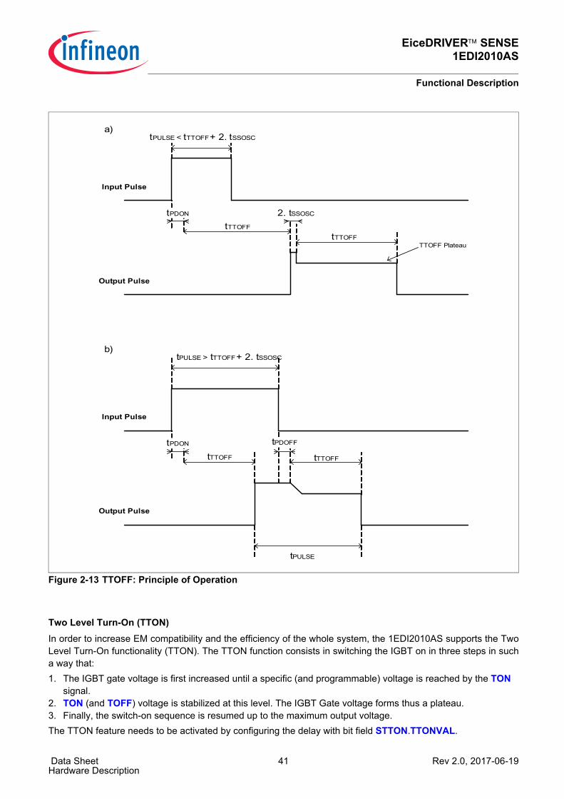
EiceDRIVER™ SENSE1EDI2010AS
Functional Description
Data Sheet 41 Rev 2.0, 2017-06-19Hardware Description
Figure 2-13 TTOFF: Principle of Operation
Two Level Turn-On (TTON)In order to increase EM compatibility and the efficiency of the whole system, the 1EDI2010AS supports the TwoLevel Turn-On functionality (TTON). The TTON function consists in switching the IGBT on in three steps in sucha way that:1. The IGBT gate voltage is first increased until a specific (and programmable) voltage is reached by the TON
signal.2. TON (and TOFF) voltage is stabilized at this level. The IGBT Gate voltage forms thus a plateau.3. Finally, the switch-on sequence is resumed up to the maximum output voltage.The TTON feature needs to be activated by configuring the delay with bit field STTON.TTONVAL.
tPULSE < tTTOFF + 2. tSSOSC
tPDON
tTTOFF
tTTOFF
Input Pulse
Output Pulse
tPULSE > tTTOFF + 2. tSSOSC
tPDON
tTTOFF
tPULSE
tPDOFF
tTTOFF
Input Pulse
Output Pulse
TTOFF Plateau
a)
b)
2. tSSOSC
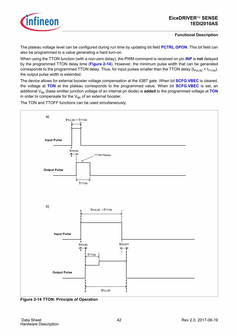
EiceDRIVER™ SENSE1EDI2010AS
Functional Description
Data Sheet 42 Rev 2.0, 2017-06-19Hardware Description
The plateau voltage level can be configured during run time by updating bit field PCTRL.GPON. This bit field canalso be programmed to a value generating a hard turn-on.When using the TTON function (with a non-zero delay), the PWM command is received on pin INP is not delayedby the programmed TTON delay time (Figure 2-14). However, the minimum pulse width that can be generatedcorresponds to the programmed TTON delay. Thus, for input pulses smaller than the TTON delay (tPULSE < tTTON),the output pulse width is extended. The device allows for external booster voltage compensation at the IGBT gate. When bit SCFG.VBEC is cleared,the voltage at TON at the plateau corresponds to the programmed value. When bit SCFG.VBEC is set, anadditional VBE (base emitter junction voltage of an internal pn diode) is added to the programmed voltage at TONin order to compensate for the VBE of an external booster.The TON and TTOFF functions can be used simultaneously.
Figure 2-14 TTON: Principle of Operation
tPULSE < tTTON
tPDON
Input Pulse
Output Pulse
TTON Plateau
a)
b)tPULSE > tTTON
tPDON
tTTON
tPULSE
tPDOFF
Input Pulse
Output Pulse
tTTON
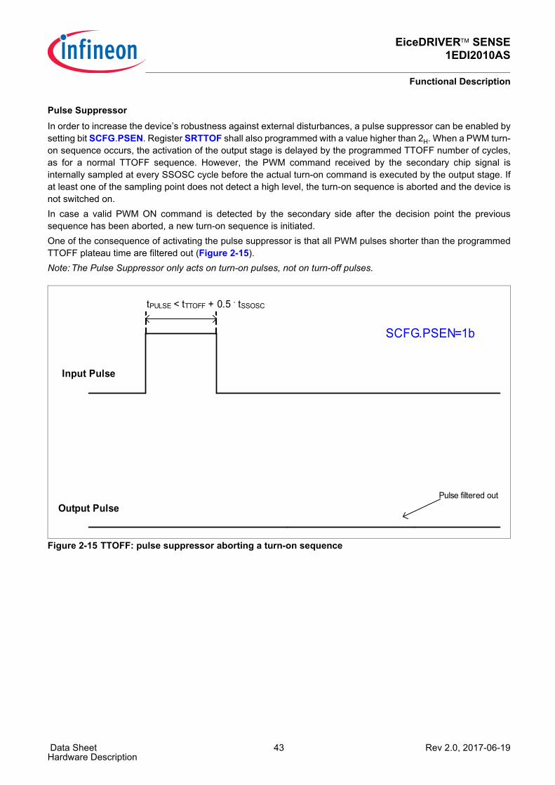
EiceDRIVER™ SENSE1EDI2010AS
Functional Description
Data Sheet 43 Rev 2.0, 2017-06-19Hardware Description
Pulse SuppressorIn order to increase the device’s robustness against external disturbances, a pulse suppressor can be enabled bysetting bit SCFG.PSEN. Register SRTTOF shall also programmed with a value higher than 2H. When a PWM turn-on sequence occurs, the activation of the output stage is delayed by the programmed TTOFF number of cycles,as for a normal TTOFF sequence. However, the PWM command received by the secondary chip signal isinternally sampled at every SSOSC cycle before the actual turn-on command is executed by the output stage. Ifat least one of the sampling point does not detect a high level, the turn-on sequence is aborted and the device isnot switched on. In case a valid PWM ON command is detected by the secondary side after the decision point the previoussequence has been aborted, a new turn-on sequence is initiated. One of the consequence of activating the pulse suppressor is that all PWM pulses shorter than the programmedTTOFF plateau time are filtered out (Figure 2-15).Note: The Pulse Suppressor only acts on turn-on pulses, not on turn-off pulses.
Figure 2-15 TTOFF: pulse suppressor aborting a turn-on sequence
tPULSE < tTTOFF + 0.5 . tSSOSC
Input Pulse
Output PulsePulse filtered out
SCFG.PSEN=1b
EiceDRIVER™ SENSE1EDI2010AS
Functional Description
Data Sheet 44 Rev 2.0, 2017-06-19Hardware Description
2.4.6.2 Switching Sequence DescriptionFigure 2-16 shows an idealized switching sequence. When a valid turn-on command is detected, a certainpropagation time tPDON is needed by the logic to transfer the PWM command to the secondary side. At this pointthe TTOFF delay time tTTOFF defined by bit field SRTTOF.RTVAL is added before the turn-on command isexecuted. Signal TON is then activated, while signal TOFF is deactivated.In case the two level turn-on function is active, signal TON is increased up to the plateau voltage defined by bitfield PCTRL.GPON. The duration tTTON between the beginning of the turn-on sequence and the moment wherethe switching sequence is resumed is defined by bit field STTON.TTONVAL. When a valid turn-off command is detected, a certain propagation time tDOFF is needed by the command to beprocessed by the logic on the secondary side. This propagation time depends on the event having generated theturn-off action (non exhaustive list):• In case of a PWM turn-off command at pin INP, tDOFF=tPDOFF.• In case of a DESAT Event, tDOFF=tOFFDESAT2.• In case of an OCP event, tDOFF=tOFFOCP2.• In case of an Event Class A on the primary side: tDOFF=tOFFCLA.• In case of an Event Class B on the secondary side: tDOFF=tOFFCLB2.When the turn-off command is processed by the logic, signals TON and TOFF are decreased with the slew ratetSLEW fixed by hardware. Once the voltage at pin TOFF has reached the value defined by bit field PCTRL2.GPOF(or SSTTOF.GPS in the case of a safe turn-off), the turn-off sequence is interrupted. Time tTTOFF is defined as themoment when the device starts turning off signal TOFF, and the moment where the turn-off sequence is resumed.Depending on the event that triggered the turn-off sequence, tTTOFF is given by either bit field SRTTOF.RTVAL orSSTTOF.STVAL. Once the TTOFF time has elapsed, a hard commutation takes place, and signals TON andTOFF are driven to VEE2.Note: Once a turn-off sequence is started, it is completed to the end with the same delay parameters.
Signal DACLP can be activated by configuring bit field SCFG.DACLC. At the moment when the hard commutationtakes place, signal DACLP remains deactivated for time tACL fixed by hardware. When this time is elapsed, signalDACLP is reactivated (i.e. active clamping is disabled). The voltage level at pin DACLP can be read at bitSSTAT2.DACL
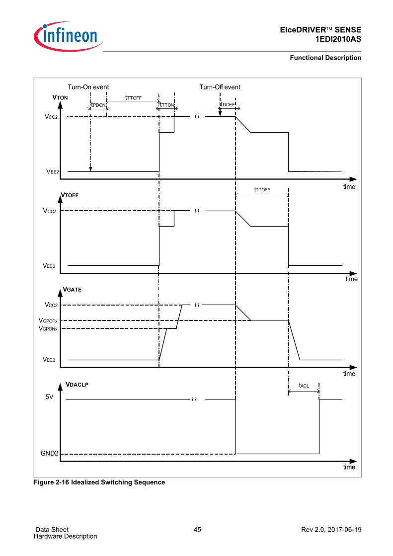
EiceDRIVER™ SENSE1EDI2010AS
Functional Description
Data Sheet 45 Rev 2.0, 2017-06-19Hardware Description
Figure 2-16 Idealized Switching Sequence
VGATE
VTON
VEE2
VEE2
VTOFF
VCC2
VEE2
Turn-On event
tPDONtTTOFF
time
time
time
5V
GND2
VDACLP
time
~ ~
Turn-Off event
tDOFF
tTTOFF~ ~VCC2
VCC2
VGPOFx
~ ~~ ~
tACL
tTTON
VGPONx

EiceDRIVER™ SENSE1EDI2010AS
Functional Description
Data Sheet 46 Rev 2.0, 2017-06-19Hardware Description
2.4.6.3 Passive ClampingWhen the secondary chip is not supplied, signals TOFF, TON and GATE are clamped to VEE2. The GATE pin isthe sensing pin for this clamping and should be not overstressed. See “Electrical Characteristic” section for theelectrical capability of this feature.
2.4.7 Fault NotificationsThe device provides two kinds of fault notification mechanisms:• Pins NFLTA, NFLTB and NRST/RDY allow for fast error notification to the main microcontroller. All signals are
active low.• Error bits can be read by SPI.The activation of signal NRST/RDY is associated with Reset Events (see Chapter 2.4.10). The activation of signalNFLTA is associated with Class A Events. The activation of signal NFLTB is associated with Class B Events. Ingeneral the activation of signal NFLTA or NFLTB is linked to a state transition of the state machine.
Handling Events Class A and BIf an Event Class A occurs that leads to a state transition (from OPM4 to OPM3 or OPM6 to OPM5), signal NFLTAis activated. In case an Event Class A occurs that does not lead to a state transition, NFLTA is not activated(exception: ADC boundary check events). However, the corresponding error bit in register PER or SER is set.ADC Boundary Check events are handled in a special way. In case bit SCFG2.ACAEN is set, an ADC BoundaryCheck event leads to an Event Class A: an Emergency (regular) turn-off sequence is issued, and possibly atransition of the state machine and the activation of NFLTA. Bit SSTAT.FLTAS (and resultingly bitPSTAT2.FLTAP) is set as long as bits SADC.AOVS or SADC.AUVS is set.In case bit SCFG2.ACAEN is cleared, an ADC Boundary Check event does not lead to a transition of the statemachine (NFLTA is not activated). Besides, no Emergency Turn-Off sequence is initiated. However, bitSER.AUVER and / or SER.AOVER is set. Therefore, when bit SCFG2.ACAEN is cleared, the ADC BoundaryCheck mechanism behaves like an Event Class C.Additionally, signal NFLTA can be activated directly by the status bits related to boundary check on the primaryside.This allows to have signal NFLTA activated in any OPM mode in case of ADC Boundary Check Events. If bitPCFG.ADAEN is set, NFLTA is activated at the transition of bit PSTAT2.AXVP from 0B to 1B.If an Event Class B occurs that leads to a state transition (to OPM1), signal NFLTB is activated. In case an EventClass B occurs that does not lead to a state transition, NFLTB is not activated. However, the corresponding errorbit in register PER or SER is set.The level issued by the device on pins NFLTA and NFLTB is given by bits PSTAT2.FLTA and PSTAT2.FLTB.The levels read by the device at those pins is given by bits PPIN.NFLTAL and PPIN.NFLTBL. In case a conditionleading to an Event Class A is detected by the device, bit PSTAT2.FLTAP is set. In case a condition leading to anEvent Class B is detected by the device, bit PSTAT2.FLTBP is set.Note: In case of short events (e.g. Desat or OCP event), it might not be possible to observe a change of the state
of bits PSTAT2.FLTAP or FLTBP.
Clearing Fault NotificationsTable 2-12 summarizes how fault notifications are cleared:
EiceDRIVER™ SENSE1EDI2010AS
Functional Description
Data Sheet 47 Rev 2.0, 2017-06-19Hardware Description
A CLRP command (i.e. setting bit PCTRL.CLRP) clears all sticky bits on the primary side. A CLRS command (i.e.setting bit PCTRL.CLRS) clears all sticky bits on the secondary side. Signals NFLTA and NFLTB are de-asserted with an invalid to valid transition of signal EN. Besides, they can bede-asserted by a CLRP command, depending on the device’ status.s•
2.4.8 EN Signal PinThe EN signal allows the logic on the primary side to have a direct control on the state of the device. A valid signalhas to be provided on this pin. A valid to invalid transition of the signal on pin EN generates an Event Class A.Pin EN should be driven actively by the external circuit. In case this pin is floating, an internal weak pull-downresistor ensures that the signal is low.Note: It should be noted that even if the signal at pin EN is valid, the device can still be in disabled state. This may
happen for example if another error is being detected
A valid EN signal is defined as a digital High level. When EN is at Low level, the signal is considered as not validand the device is in Disabled State. In case of a High-to-Low transition, an Event Class A is generated.An Invalid to Valid transition of signal EN deactivates signals NFLTA and NFLTB (when the device is in OPM3 orOPM5 only).The levels read by the device at pin EN is given by bits PPIN.ENL. The validity status of EN signal is given by bitPSTAT2.ENVAL.
Table 2-12 Failure Notification ClearingNFLTA / B signals Primary Sticky Bits Secondary Sticky Bits
PCTRL.CLRP set De-assertion Cleared -PCTRL.CLRS set 1)
1) If the device is in OPM1, setting bit SCTRL.CLRS leads to a transition to OPM0
- - ClearedEN Invalid to Valid transition De-assertion 2)
2) Only in OPM3 and OPM5. In other Operating Modes, no de-assertion is done.
- -

EiceDRIVER™ SENSE1EDI2010AS
Functional Description
Data Sheet 48 Rev 2.0, 2017-06-19Hardware Description
2.4.9 Internal SupervisionThe Internal Supervision functionality is summarized in Table 2-13:
The primary and secondary chips are equipped with internal verification mechanisms ensuring that the keyfunctions of the device are operating correctly. The internal blocks which are supervised are listed below:• Lifesign watchdog: mutual verification of the response of both chips (both primary and secondary).• Oscillators (both primary and secondary, including open / short detection on signals IREF1).• Memory error (both primary and secondary).
2.4.9.1 Lifesign watchdogThe primary and the secondary chips monitor each other by the mean of a lifesign signal. The periodicity of thelifesign is typically tLS. Each chip expects a lifesign from its counterpart within a given time window. In case alifesign error is detected by a chip, a reset event is generated on both sides (lead to OPM0) as well as NFLTB pinis set. Due to the communication loss on both sides both bits PER.CERP and SER.CERS are set.Note: Bits PER.CERP and SER.CERS indicate a loss of communication event. The current status of the internal
communication is indicated by bit PSTAT.SRDY.
2.4.9.2 Oscillator MonitoringThe main oscillators on the primary and on the secondary side are monitored continuously. Two distinctmechanisms are used for this purpose:• Lifesign Watchdog allows to detect significant deviations from the nominal frequency (both primary and
secondary, see above).• Open / short detection on pin IREF1.In case a failure is detected on pin IREF1, the primary chip is kept in reset state for the duration of the failure andsignal NRST/RDY is asserted, This leads to the detection of a lifesign error by the secondary chip, generating thusan reset event.
2.4.9.3 Memory SupervisionThe configuration parameters of the device, stored in the registers, are protected with a parity bit protectionmechanism. Both primary and secondary chips are protected (refer to Chapter 4).In case a failure is detected on the primary chip, it is kept in reset state, and both signal NRST/RDY and NFLTBare asserted. The secondary side initiates an Emergency (Regular) Turn-Off sequence.In case a memory failure is detected by the secondary chip, an Emergency (Regular) Turn-Off sequence isinitiated. The secondary chip is kept in reset state for the duration of the failure. This leads to the detection of alifesign error by the primary chip, generating thus an reset event.
Table 2-13 System Supervision OverviewParameter Short DescriptionFunction Monitoring of the key internal functions of the chip.Periodicity Continuous.Action in case of failure event See belowProgrammability No.

EiceDRIVER™ SENSE1EDI2010AS
Functional Description
Data Sheet 49 Rev 2.0, 2017-06-19Hardware Description
2.4.9.4 Hardware Failure BehaviorThe internal supervision function can detect several failures which could lead to primary or secondary chip holdon (stay in reset). Failures which can be detected are mentioned in the table below. The supervision functionsdescribed in the chapters before will lead to this behavior.
Table 2-14 Failure Events SummaryFailure Event Primary Secondary Notification
(primary)Notification(secondary)
OSC1 not starting at power-up
Reset Soft Reset • NRST/RDY Low (driven by device during event).
• Bit PER.RSTP set (once OSC1 valid again).
• Bit PER.CERP is not set.• NFLTB activated at the
end of the reset event.
• Bit SER.CERS set (in case of lifesign lost).
• Output Stage issues a PWM OFF command.
IREF1 shorted to ground or open
Reset Soft Reset • NRST/RDY Low (driven by device during event).
• Bit PER.RSTP set (once IREF1 valid again).
• Bit PER.CERP is not set.• NFLTB activated at the
end of the reset event.
• Bit SER.CERS set (in case of lifesign lost).
• Output Stage issues a PWM OFF command.
Memory error on primary
Reset Soft Reset • NRST/RDY Low (driven by device during event).
• Bit PER.RSTP set (when failure condition is removed).
• Bit PER.CERP is not set.• NFLTB activated at the
end of the reset event.
• Bit SER.CERS set (in case of lifesign lost).
• Output Stage issues a PWM OFF command.
OSC2 not starting at power-up
- Hard Reset • NFLTB activated, bit PER.CERP set.
• Bit PSTAT.SRDY cleared
• Output Stage issues a PWM OFF command.
OSC2 misfunction during operation
- Soft Reset • NFLTB activated, bit PER.CERP set.
• Bit PSTAT.SRDY cleared for the duration of the failure.
• Output Stage issues a PWM OFF command.
VREG shorted to ground
- Hard Reset • NFLTB activated, bit PER.CERP set.
• Bit PSTAT.SRDY cleared.
• Output Stage issues a PWM OFF command.
• Bit SER.RSTS (once VCC2 valid again).
Memory error on secondary
- Hard Reset • NFLTB activated, bit PER.CERP set.
• Bit PSTAT.SRDY cleared.
• Output Stage issues a PWM OFF command.
EiceDRIVER™ SENSE1EDI2010AS
Functional Description
Data Sheet 50 Rev 2.0, 2017-06-19Hardware Description
2.4.10 Reset EventsA reset event sets the device and its internal logic in the default configuration. All user-defined settings areoverwritten with the default values. The list of reset events and their effect is summarized in Table 2-15.
All reset events set the device in Mode OPM0. In a soft reset, the logic works further, but the registers use thedefault values.In case of a reset condition on the primary side, the behavior of the pin of the device is defined in Table 2-16.
In case of a hard reset condition on the secondary side, the behavior of the pin of the device is defined inTable 2-17.
Table 2-15 Reset Events SummaryReset Event Primary Secondary Notification
(primary)Notification(secondary)
NRST/RDY input signal active (driven externally)
Reset Soft Reset • NRST/RDY Low (during event).
• Bit PER.RSTEP and PER.RSTP set.
• Bit PER.CERP is not set.• NFLTB activated at the
end of the reset event.
• Bit SER.CERS set (in case of lifesign lost).
• Output Stage issues a PWM OFF command.
UVLO1 Event Reset Soft Reset • NRST/RDY Low (driven by device during event).
• Bit PER.RSTP set (once VCC1 valid again).
• Bit PER.CERP is not set.• NFLTB activated at the
end of the reset event.
• Bit SER.CERS set (in case of lifesign lost).
• Output Stage issues a PWM OFF command.
VCC2 reset event (communication loss due to voltage breakdown on VCC2 )
- Hard Reset • NFLTB activated, bit PER.CERP set.
• Bit PSTAT.SRDY cleared for the duration of the failure.
• Bit SER.RSTS (once VCC2 valid again).
• Output Stage issues a PWM OFF command.
Table 2-16 Pin behavior (primary side) in case of reset conditionPin Output Level CommentsSDO TristateNFLTB LowNFLTA LowNRST/RDY Low (GND1)
Table 2-17 Pin behavior (secondary side) in case of reset conditionPin Output Level CommentsTON Low (VEE2) Passive ClampingTOFF Low (VEE2) Passive ClampingDESAT Low (GND2) Clamped.

EiceDRIVER™ SENSE1EDI2010AS
Functional Description
Data Sheet 51 Rev 2.0, 2017-06-19Hardware Description
2.4.11 Operation in Configuration ModeThis section describes the mechanisms to configure the device.
2.4.11.1 Static Configuration ParametersStatic parameters can configured when the device is in Mode OPM2 by writing the appropriate configurationregister.Once Mode OPM2 is left with the SPI Command EXIT_CMODE, the configuration parameters are frozen on bothprimary and secondary chips. This means in particular that write accesses to the corresponding registers areinvalidated. This prevents static configurations to be modified during runtime. Besides, the configurationparameters on the primary and secondary side are protected with a memory protection mechanism. In case thevalues are not consistent, a Reset Event and / or an Event Class B is generated.
2.4.11.1.1 Configuration of the SPI Parity CheckThe SPI interface supports by default an odd parity check. The Parity Check mechanism (active at the receptionof an SPI word) can be disabled by setting bit PCFG.PAREN to 0B. Setting bit PAREN to 1B enables the ParityCheck.Parity Bit Generation for the transmitter can not be disabled.
2.4.11.1.2 Configuration of NFLTA and NFLTB clear modeThe reaction of signals NFLTA and NFLTB to a clear primary command is defined by the values of respectivelybits PCFG.CLFAM and PCFG.CLFBM. See Chapter 2.4.7 for more details.
2.4.11.1.3 Configuration of NFLTA activation in case of Boundary Check eventSignal NFLTA is normally activated by a state transition of the internal state machine. However, it can also beconfigured to be activated in relation with bit PSTAT2.AXVP. This is configured thanks to bit PCFG.ADAEN.
2.4.11.1.4 Configuration of pin ADCT Signal ADCT can be used as a trigger source for the ADC on the secondary side. If PCFG.ADTEN is cleared, thevoltage read on the pin is ignored by the device. If PCFG.ADTEN is set, an ADC conversion is triggered at a risingedge detected at pin ADCT.
GATE Low (VEE2) Passive ClampingDACLP High (5V)
Table 2-17 Pin behavior (secondary side) in case of reset conditionPin Output Level Comments
EiceDRIVER™ SENSE1EDI2010AS
Functional Description
Data Sheet 52 Rev 2.0, 2017-06-19Hardware Description
2.4.11.1.5 Configuration of the STP Minimum Dead TimeThe minimum dead time for the Shoot-Through Protection can be programmed by writing bit fieldPCFG2.STPDEL. The value programmed corresponds to a number of OSC1 clock cycles.
2.4.11.1.6 Configuration of the Digital ChannelThe direction of pin can be programmed by writing bit field PCFG2.DIO1. The direction of pin DIO2 can beprogrammed by writing bit field SCFG.DIO2C.
2.4.11.1.7 Configuration of the VBE CompensationThe VBE compensation of signal TON and TOFF can be activated or deactivated by writing bit SCFG.VBEC. SeeChapter 2.4.6 for more details.
2.4.11.1.8 Clamping of DESAT pinBy setting bit SCFG.DSTCEN, the DESAT signal is clamped to VGND2 while the output stage of the device issuesa PWM OFF command and during blanking time periods. By clearing bit SCFG.DSTCEN, the DESAT clamping isonly activated during blanking time periods.
2.4.11.1.9 Activation of the Pulse SuppressorThe pulse suppressor function is associated with the TTOFF function and can be activated by setting bitSCFG.PSEN. When activated, SRTTOF.RTVAL shall be programmed with a minimum value.
2.4.11.1.10 Configuration of the Verification Mode Time Out DurationThe duration of the time out in verification mode is selectable via bit SCFG.TOSEN.
2.4.11.1.11 DESAT Threshold Level ConfigurationThe detection level of the DESAT comparator is selectable via bit SCFG.DSATLS.
2.4.11.1.12 UVLO2 Threshold Level ConfigurationThe detection levels of the UVLO2 comparators are selectable via bit SCFG.UVLO2S.
2.4.11.1.13 DACLP Operating Mode ConfigurationThe operating mode of pin DACLP is selectable via bit field SCFG.DACLC.
2.4.11.1.14 Configuration of the ADCThe configuration of the ADC is selectable by writing register SCFG2. The limits of the boundary checker areselectable by writing register SBC.Note: Registers SCFG2 and SBC can only be written if bit SCFG.CFG2 is set to 1B.
EiceDRIVER™ SENSE1EDI2010AS
Functional Description
Data Sheet 53 Rev 2.0, 2017-06-19Hardware Description
2.4.11.1.15 Configuration of the DESAT Blanking TimeThe blanking time for the DESAT protection can be configured by writing bit field SDESAT.DSATBT. A minimumvalue for the blanking time has to be programmed.Note: The programmed OCP blanking time shall be smaller than the programmed DESAT blanking time.
2.4.11.1.16 Configuration of the OCP FunctionThe blanking time for the OCP protection can be configured by writing bit field SOCP.OCPBT. Programming 0Hdeactivates the blanking time feature. In case a blanking time is required, a minimum value for the delay has to beprogrammed. The detection level of the OCP comparator is selectable via bit SCFG.OCPLS.Note: The programmed OCP blanking time shall be smaller than the programmed DESAT blanking time.
2.4.11.1.17 Configuration of the TTOFF sequencesThe TTOFF delays for Regular and Safe Turn-Off sequences can be programmed separately by writing registersSRTTOF or SSTTOF. The delay for Regular Turn-Off can also be configured using the Timing Calibration Feature.Programming 0H as a delay value disables the TTOFF for the concerned Turn-Off Sequence. Hard turn-off areperformed instead. In case the TTOFF function is wished, a minimum value for the delay has to be programmed.When safe two level turn-off is used (non zero delay) in normal operating mode (OPM4), the programmed safeturn-off delay value shall be higher than the programmed regular two level turn of delay.The plateau level for safe two level turn off sequences can be programmed with bit field SSTTOF.GPS. Theplateau level value for safe turn-off sequences shall be lower than the one selected for regular turn-off sequences.The regular TTOFF delay can be calibrated using the TCF feature of the device.
2.4.11.1.18 Configuration of the TTON Delay TO UpdateThe TTON delay can be configured by writing bit field STTON.TTONVAL. Programming 0H as a delay valuedisables the TTON for all turn-on sequences. Hard turn-on are performed instead. In case the TTON function iswished, a minimum value for the delay has to be programmed.The TTON delay can be calibrated using the TCF feature of the device.
2.4.11.2 Dynamic ConfigurationThe TTOFF (regular turn-off only) plateau level can be modified during runtime by writing bit field PCTRL2.GPOF.The value of this bit field is periodically transferred to the secondary side. The last valid received value by theprimary side is available at bit field PSTAT.GPOFP. The value currently used by the secondary chip is availableat bit field SCTRL.GPOFS.Similarly, The WTO and the TTON plateau level can be configured by writing bit field PCTRL.GPON. The valueof this bit field is periodically transferred to the secondary side. The last valid received value by the primary sideis available at bit field PSTAT.GPONP. The value currently used by the secondary chip is available at bit fieldSCTRL.GPONS.The plateau value stored in the device at the beginning of the corresponding switching sequence is latched andactive until the upper next switching sequence.
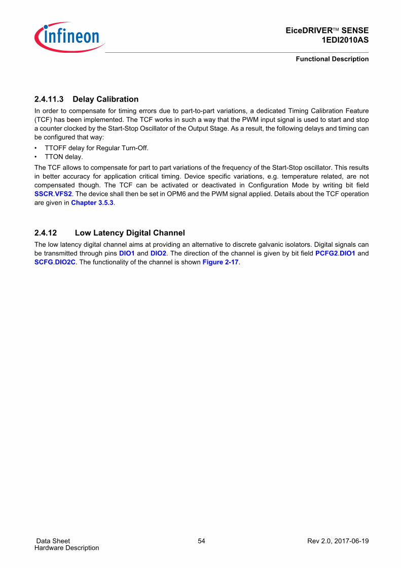
EiceDRIVER™ SENSE1EDI2010AS
Functional Description
Data Sheet 54 Rev 2.0, 2017-06-19Hardware Description
2.4.11.3 Delay CalibrationIn order to compensate for timing errors due to part-to-part variations, a dedicated Timing Calibration Feature(TCF) has been implemented. The TCF works in such a way that the PWM input signal is used to start and stopa counter clocked by the Start-Stop Oscillator of the Output Stage. As a result, the following delays and timing canbe configured that way:• TTOFF delay for Regular Turn-Off.• TTON delay.The TCF allows to compensate for part to part variations of the frequency of the Start-Stop oscillator. This resultsin better accuracy for application critical timing. Device specific variations, e.g. temperature related, are notcompensated though. The TCF can be activated or deactivated in Configuration Mode by writing bit fieldSSCR.VFS2. The device shall then be set in OPM6 and the PWM signal applied. Details about the TCF operationare given in Chapter 3.5.3.
2.4.12 Low Latency Digital ChannelThe low latency digital channel aims at providing an alternative to discrete galvanic isolators. Digital signals canbe transmitted through pins DIO1 and DIO2. The direction of the channel is given by bit field PCFG2.DIO1 andSCFG.DIO2C. The functionality of the channel is shown Figure 2-17.
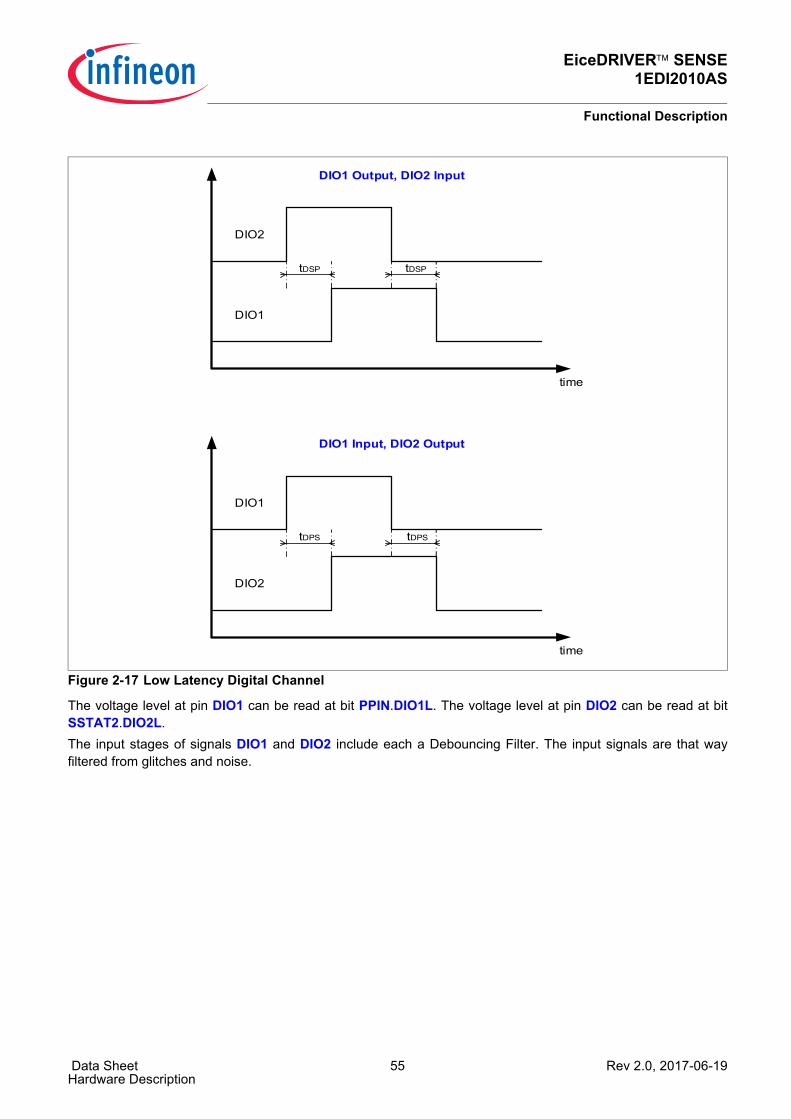
EiceDRIVER™ SENSE1EDI2010AS
Functional Description
Data Sheet 55 Rev 2.0, 2017-06-19Hardware Description
Figure 2-17 Low Latency Digital Channel
The voltage level at pin DIO1 can be read at bit PPIN.DIO1L. The voltage level at pin DIO2 can be read at bitSSTAT2.DIO2L.The input stages of signals DIO1 and DIO2 include each a Debouncing Filter. The input signals are that wayfiltered from glitches and noise.
DIO1 Output, DIO2 Input
DIO2
tDSP
time
tDSP
DIO1
DIO1 Input, DIO2 Output
DIO1
tDPS
time
tDPS
DIO2
EiceDRIVER™ SENSE1EDI2010AS
Functional Description
Data Sheet 56 Rev 2.0, 2017-06-19Hardware Description
2.4.13 Analog Digital Converter
2.4.13.1 OverviewThe key properties of the built-in ADC on the secondary side are:• Successive Approximation method.• 0V to 5 V input signal (input buffer).• 8-bit resolution.• Fast conversion time.• Preamplifier with programmable gain.• Selectable offset.The ADC operates by the method of the successive approximation. The ADC offers a flexible analog measurementcapability, which fulfills the following functions (non exhaustive list):• Measurement of a NTC resistor located on the power module (Figure 2-18).• Measurement of a temperature diode integrated into the IGBT (Figure 2-19).• Measurement of the high voltage DC-Link or phase voltage (Figure 2-20).
Figure 2-18 Application Example NTC Measurement
.
AIP
GND
AIN
NTCADCT
Device
ADC
Logic
VINT IAIPCS
GAINi
VOFFSETi
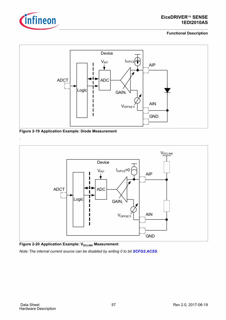
EiceDRIVER™ SENSE1EDI2010AS
Functional Description
Data Sheet 57 Rev 2.0, 2017-06-19Hardware Description
Figure 2-19 Application Example: Diode Measurement
.
Figure 2-20 Application Example: VDCLINK Measurement
Note: The internal current source can be disabled by writing 0 to bit SCFG2.ACSS.
ADCT
AIP
Device
ADC
Logic
AIN
GND
VINT IAIPCS
GAINi
VOFFSETi
VDCLINK
AIP
GND
AIN
ADCT
Device
ADC
Logic
VINT IAIPCS=0
GAINi
VOFFSETi
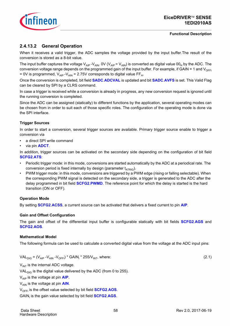
EiceDRIVER™ SENSE1EDI2010AS
Functional Description
Data Sheet 58 Rev 2.0, 2017-06-19Hardware Description
2.4.13.2 General OperationWhen it receives a valid trigger, the ADC samples the voltage provided by the input buffer.The result of theconversion is stored as a 8-bit value.The input buffer captures the voltage VAIP -VAIN. 0V (VAIP = VAIN) is converted as digital value 00H by the ADC. Theconversion voltage range depends on the programmed gain of the input buffer. For example, if GAIN = 1 and VOFFi= 0V is programmed, VAIP -VAIN = 2.75V corresponds to digital value FFH.Once the conversion is completed, bit field SADC.ADCVAL is updated and bit SADC.AVFS is set. This Valid Flagcan be cleared by SPI by a CLRS command.In case a trigger is received while a conversion is already in progress, any new conversion request is ignored untilthe running conversion is completed.Since the ADC can be assigned (statically) to different functions by the application, several operating modes canbe chosen from in order to suit each of those specific roles. The configuration of the operating mode is done viathe SPI interface.
Trigger SourcesIn order to start a conversion, several trigger sources are available. Primary trigger source enable to trigger aconversion via• a direct SPI write command• via pin ADCT.In addition, trigger sources can be activated on the secondary side depending on the configuration of bit fieldSCFG2.ATS:• Periodic trigger mode: in this mode, conversions are started automatically by the ADC at a periodical rate. The
conversion period is fixed internally by design (parameter tATRIG).• PWM trigger mode: in this mode, conversions are triggered by a PWM edge (rising or falling selectable). When
the corresponding PWM signal is detected on the secondary side, a trigger is generated to the ADC after the delay programmed in bit field SCFG2.PWMD. The reference point for which the delay is started is the hard transition (ON or OFF).
Operation ModeBy setting SCFG2.ACSS, a current source can be activated that delivers a fixed current to pin AIP.
Gain and Offset ConfigurationThe gain and offset of the differential input buffer is configurable statically with bit fields SCFG2.AGS andSCFG2.AOS.
Mathematical ModelThe following formula can be used to calculate a converted digital value from the voltage at the ADC input pins:
VALDIG = (VAIP -VAIN -VOFFi) * GAINi * 255/VINT, where: (2.1)
VINT is the internal ADC voltage. VALDIG is the digital value delivered by the ADC (from 0 to 255).VAIP is the voltage at pin AIP.VAIN is the voltage at pin AIN.VOFFi is the offset value selected by bit field SCFG2.AOS.GAINi is the gain value selected by bit field SCFG2.AGS.

EiceDRIVER™ SENSE1EDI2010AS
Functional Description
Data Sheet 59 Rev 2.0, 2017-06-19Hardware Description
2.4.13.3 Boundary CheckThe Boundary Check mechanism automatically compares each conversion result to two boundary values. Theresult of the conversion is compared to the limits specified by bit fields SBC.LCB1A (lower limit) and LCB1B(upper limit).When a new conversion result is available, the result is compared with the boundary values stored in register SBC.The values used for the comparison are respectively SBC.LCB1A extended by the LSBs 0B0B (i.e.: (LCB1A <<2)& FCH ) and SBC.LCB1B extended by the LSBs 1B1B (ie: (LCB1B << 2) | 03H ).In case the conversion result is below each of the boundaries, error flag SER.AUVER is set. In case the conversionresult is above each of the boundaries, error flag SER.AOVER is set. In case the conversion result is above orequal one boundary and below or equal the other boundary, no flag is set. (If lower and upper limit areprogrammed in the other way around the device gives wrong limit cross notifications .)The default limits are chosen such that the flags are never set whatever the conversion result is (equivalent todisabling the limit check).The failure reaction of the device to a Boundary Check event can be programed with bit SCFG2.ADAEN.
EiceDRIVER™ SENSE1EDI2010AS
Protection and Diagnostics
Data Sheet 60 Rev 2.0, 2017-06-19Hardware Description
3 Protection and DiagnosticsThis section can describes the safety relevant functions implemented in the 1EDI2010AS.
3.1 Supervision OverviewThe 1EDI2010AS driver provides extended supervision functions, in order to support safety strategies on systemlevel. Table 3-1 gives an overview of the implemented functions.
From the conceptual point of view, the protection functions can be clustered into five main categories.• Category A corresponds to the functions where the device “decides on its own”, after the detection of an Event
Class A, to change the state of the output stage and to disable itself. A dedicated action from the user is needed to reactivate the device (fast reactivation).
• Category B corresponds to the functions where the device “decides on its own”, after the detection of an Event Class B, to change the state of the output stage and to disable itself. A complete reinitialization from the user is needed to reactivate the device (slow reactivation).
• Category C corresponds to the functions that only issue a notification in case an error is detected.• Category D are intrusive supervision functions, aimed at being started when the application is not running.• Category E corresponds to implemented functions or capabilities supported by the device whose use can
enhance the overall safety coverage of the application.
Table 3-1 Safety Related Functions Protection Feature Description Cate-
goryComments
DESAT Monitoring of the collector-emitter voltage of the IGBT in ON state.
A See Chapter 3.2.1
OCP Monitoring of the current on the IGBT’s auxiliary emitter path.
A See Chapter 3.2.2
External Enable Fast deactivation via an external Enable signal on the primary.
A See Chapter 3.2.3
ADC Boundary Check ADC Boundary Check A See Chapter 2.4.13.3Power Supply Monitoring
Under Voltage Lock-Out function on VCC1, VCC2. B See Chapter 3.3.1
STP Shoot Through Protection. C See Chapter 3.4.1
SPI Error Detection SPI Error Detection. C See Chapter 3.4.2
WTO Weak Turn-On Functionality D See Chapter 3.5.2
Internal Clock Supervision
Plausibility check of the frequency of the internal oscillator.
D See Chapter 3.5.3
TTOFF Two Level Turn-Off E See Chapter 2.4.6
SPI Communication SPI Communication (using register PRW). E See Chapter 4.1
Overvoltage robustness Robustness against transient overvoltage on power supply.
E See Chapter 5.2
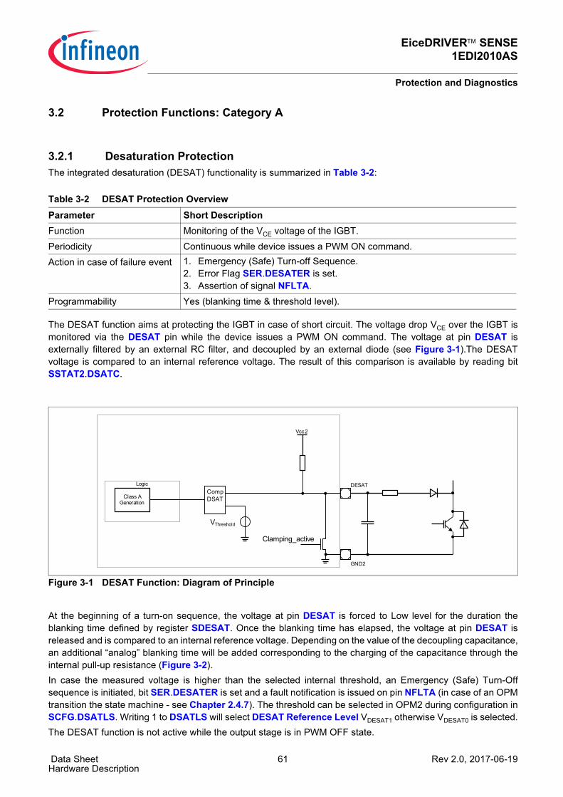
EiceDRIVER™ SENSE1EDI2010AS
Protection and Diagnostics
Data Sheet 61 Rev 2.0, 2017-06-19Hardware Description
3.2 Protection Functions: Category A
3.2.1 Desaturation ProtectionThe integrated desaturation (DESAT) functionality is summarized in Table 3-2:
The DESAT function aims at protecting the IGBT in case of short circuit. The voltage drop VCE over the IGBT ismonitored via the DESAT pin while the device issues a PWM ON command. The voltage at pin DESAT isexternally filtered by an external RC filter, and decoupled by an external diode (see Figure 3-1).The DESATvoltage is compared to an internal reference voltage. The result of this comparison is available by reading bitSSTAT2.DSATC.
Figure 3-1 DESAT Function: Diagram of Principle
At the beginning of a turn-on sequence, the voltage at pin DESAT is forced to Low level for the duration theblanking time defined by register SDESAT. Once the blanking time has elapsed, the voltage at pin DESAT isreleased and is compared to an internal reference voltage. Depending on the value of the decoupling capacitance,an additional “analog” blanking time will be added corresponding to the charging of the capacitance through theinternal pull-up resistance (Figure 3-2).In case the measured voltage is higher than the selected internal threshold, an Emergency (Safe) Turn-Offsequence is initiated, bit SER.DESATER is set and a fault notification is issued on pin NFLTA (in case of an OPMtransition the state machine - see Chapter 2.4.7). The threshold can be selected in OPM2 during configuration inSCFG.DSATLS. Writing 1 to DSATLS will select DESAT Reference Level VDESAT1 otherwise VDESAT0 is selected.The DESAT function is not active while the output stage is in PWM OFF state.
Table 3-2 DESAT Protection OverviewParameter Short DescriptionFunction Monitoring of the VCE voltage of the IGBT.Periodicity Continuous while device issues a PWM ON command.Action in case of failure event 1. Emergency (Safe) Turn-off Sequence.
2. Error Flag SER.DESATER is set.3. Assertion of signal NFLTA.
Programmability Yes (blanking time & threshold level).
CompDSAT
VThreshold
Class A Generation
Logic
Vcc2
DESAT
Clamping_active
GND2
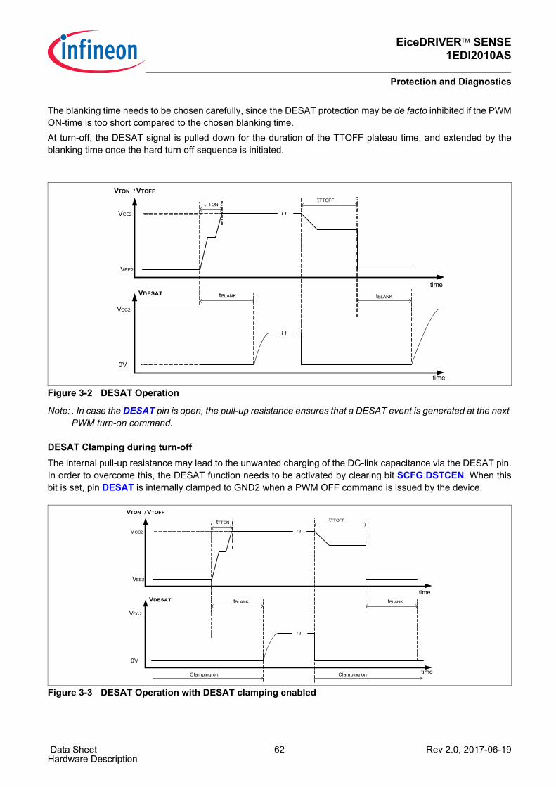
EiceDRIVER™ SENSE1EDI2010AS
Protection and Diagnostics
Data Sheet 62 Rev 2.0, 2017-06-19Hardware Description
The blanking time needs to be chosen carefully, since the DESAT protection may be de facto inhibited if the PWMON-time is too short compared to the chosen blanking time.At turn-off, the DESAT signal is pulled down for the duration of the TTOFF plateau time, and extended by theblanking time once the hard turn off sequence is initiated.
Figure 3-2 DESAT Operation
Note: . In case the DESAT pin is open, the pull-up resistance ensures that a DESAT event is generated at the next PWM turn-on command.
DESAT Clamping during turn-offThe internal pull-up resistance may lead to the unwanted charging of the DC-link capacitance via the DESAT pin.In order to overcome this, the DESAT function needs to be activated by clearing bit SCFG.DSTCEN. When thisbit is set, pin DESAT is internally clamped to GND2 when a PWM OFF command is issued by the device.
Figure 3-3 DESAT Operation with DESAT clamping enabled
VTON / VTOFF
VEE2
VDESAT
VCC2
0V
time
time
tTTOFF
VCC2
~ ~~ ~
tBLANK tBLANK
tTTON
VTON / VTOFF
VEE2
VDESAT
VCC2
0V
time
time
tTTOFF
VCC2
~ ~~ ~
tBLANK
tTTON
Clamping on Clamping on
tBLANK
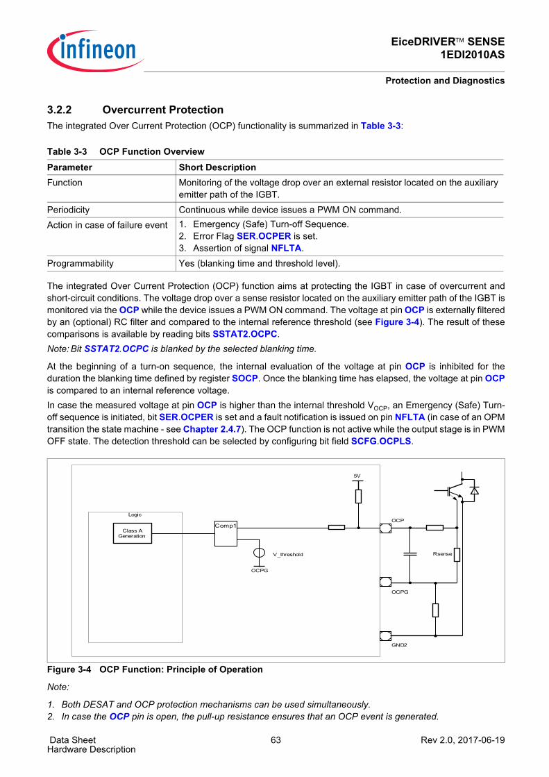
EiceDRIVER™ SENSE1EDI2010AS
Protection and Diagnostics
Data Sheet 63 Rev 2.0, 2017-06-19Hardware Description
3.2.2 Overcurrent ProtectionThe integrated Over Current Protection (OCP) functionality is summarized in Table 3-3:
The integrated Over Current Protection (OCP) function aims at protecting the IGBT in case of overcurrent andshort-circuit conditions. The voltage drop over a sense resistor located on the auxiliary emitter path of the IGBT ismonitored via the OCP while the device issues a PWM ON command. The voltage at pin OCP is externally filteredby an (optional) RC filter and compared to the internal reference threshold (see Figure 3-4). The result of thesecomparisons is available by reading bits SSTAT2.OCPC.Note: Bit SSTAT2.OCPC is blanked by the selected blanking time.
At the beginning of a turn-on sequence, the internal evaluation of the voltage at pin OCP is inhibited for theduration the blanking time defined by register SOCP. Once the blanking time has elapsed, the voltage at pin OCPis compared to an internal reference voltage.In case the measured voltage at pin OCP is higher than the internal threshold VOCP, an Emergency (Safe) Turn-off sequence is initiated, bit SER.OCPER is set and a fault notification is issued on pin NFLTA (in case of an OPMtransition the state machine - see Chapter 2.4.7). The OCP function is not active while the output stage is in PWMOFF state. The detection threshold can be selected by configuring bit field SCFG.OCPLS.
Figure 3-4 OCP Function: Principle of Operation
Note:
1. Both DESAT and OCP protection mechanisms can be used simultaneously.2. In case the OCP pin is open, the pull-up resistance ensures that an OCP event is generated.
Table 3-3 OCP Function OverviewParameter Short DescriptionFunction Monitoring of the voltage drop over an external resistor located on the auxiliary
emitter path of the IGBT.Periodicity Continuous while device issues a PWM ON command.Action in case of failure event 1. Emergency (Safe) Turn-off Sequence.
2. Error Flag SER.OCPER is set.3. Assertion of signal NFLTA.
Programmability Yes (blanking time and threshold level).
OCPComp1
V_threshold
Class A Generation
Logic
OCPG
5V
OCPG
Rsense
GND2
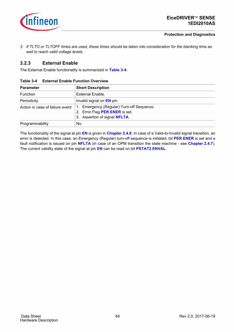
EiceDRIVER™ SENSE1EDI2010AS
Protection and Diagnostics
Data Sheet 64 Rev 2.0, 2017-06-19Hardware Description
3. If TLTO or TLTOFF times are used, these times should be taken into consideration for the blanking time as well to reach valid voltage levels.
3.2.3 External EnableThe External Enable functionality is summarized in Table 3-4:
The functionality of the signal at pin EN is given in Chapter 2.4.8. In case of a Valid-to-Invalid signal transition, anerror is detected. In this case, an Emergency (Regular) turn-off sequence is initiated, bit PER.ENER is set and afault notification is issued on pin NFLTA (in case of an OPM transition the state machine - see Chapter 2.4.7).The current validity state of the signal at pin EN can be read on bit PSTAT2.ENVAL.
Table 3-4 External Enable Function OverviewParameter Short DescriptionFunction External Enable.Periodicity Invalid signal on EN pin.Action in case of failure event 1. Emergency (Regular) Turn-off Sequence.
2. Error Flag PER.ENER is set.3. Assertion of signal NFLTA.
Programmability No.

EiceDRIVER™ SENSE1EDI2010AS
Protection and Diagnostics
Data Sheet 65 Rev 2.0, 2017-06-19Hardware Description
3.3 Protection Functions: Category B
3.3.1 Power Supply Voltage MonitoringThe Power Supply Voltage Monitoring functionality is summarized in Table 3-5:
In order to ensure a correct switching of the IGBT, the device supports an undervoltage lockout (UVLO) functionfor VCC1 and VCC2.The VCC1 voltage is compared (using an internal voltage comparator) to an internal reference threshold. If thepower supply voltage VCC1 of the primary chip drops below VUVLO1L, an error is detected. In this case, anemergency (Regular) turn-off sequence is initiated and signal NRST/RDY goes low. In case VCC1 reachesafterwards a level higher than VUVLO1H, then the error condition is removed and signal NRST/RDY is deasserted.Besides, bit PER.RSTP is set.The VCC2 voltage is compared (using an internal voltage comparator) to an internal reference threshold. If thepower supply voltage VCC2 of the secondary chip drops below VUVLO2L, an error is detected. In this case, anemergency (Regular) turn-off sequence is initiated, bit SER.UVLO2ER is set and signal NFLTB is activated (incase of an OPM transition the state machine - see Chapter 2.4.7). In case VCC2 reaches afterwards a level higherthan VUVLO2H, then the error condition is removed and the device can be reenabled. The level of UVLO2 can beadjusted via configuration of SCFG.UVLO2S to fit lower supply voltage.The current status of the error detection of UVLO2 mechanism is available by reading bit SSTAT2.UVLO2M.Note: In case VCC2 goes below the voltage VRST2, the secondary chip is kept in reset state.
Table 3-5 Power Supply Voltage Monitoring OverviewParameter Short DescriptionFunction Monitoring of VCC1, VCC2.Periodicity Continuous.Action in case of failure event 1. Emergency (Regular) Turn-off Sequence.
2. Error Flag PER.RSTP (UVLO1) or SER.UVLO2ER (UVLO2).3. Assertion of signal NRST/RDY (UVLO1) or NFLTB (UVLO2).
Programmability Yes(UVLO2 threshold level).
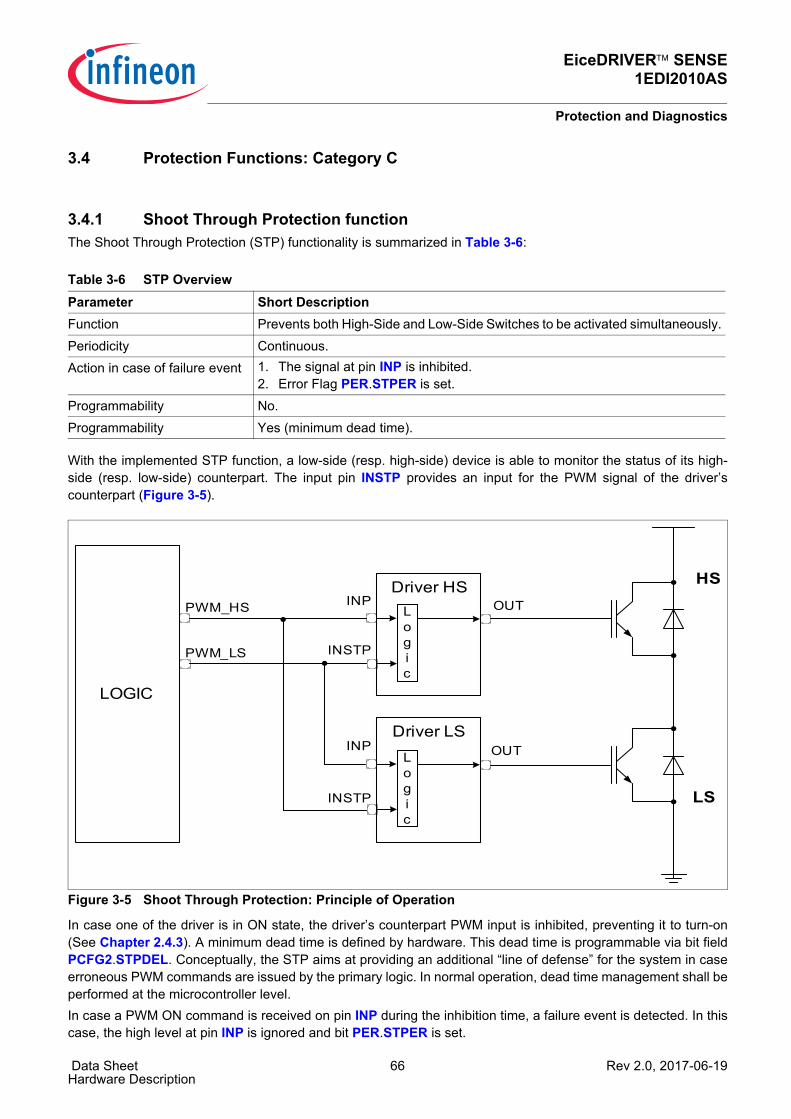
EiceDRIVER™ SENSE1EDI2010AS
Protection and Diagnostics
Data Sheet 66 Rev 2.0, 2017-06-19Hardware Description
3.4 Protection Functions: Category C
3.4.1 Shoot Through Protection functionThe Shoot Through Protection (STP) functionality is summarized in Table 3-6:
With the implemented STP function, a low-side (resp. high-side) device is able to monitor the status of its high-side (resp. low-side) counterpart. The input pin INSTP provides an input for the PWM signal of the driver’scounterpart (Figure 3-5).
Figure 3-5 Shoot Through Protection: Principle of Operation
In case one of the driver is in ON state, the driver’s counterpart PWM input is inhibited, preventing it to turn-on(See Chapter 2.4.3). A minimum dead time is defined by hardware. This dead time is programmable via bit fieldPCFG2.STPDEL. Conceptually, the STP aims at providing an additional “line of defense” for the system in caseerroneous PWM commands are issued by the primary logic. In normal operation, dead time management shall beperformed at the microcontroller level.In case a PWM ON command is received on pin INP during the inhibition time, a failure event is detected. In thiscase, the high level at pin INP is ignored and bit PER.STPER is set.
Table 3-6 STP OverviewParameter Short DescriptionFunction Prevents both High-Side and Low-Side Switches to be activated simultaneously.Periodicity Continuous.Action in case of failure event 1. The signal at pin INP is inhibited.
2. Error Flag PER.STPER is set.Programmability No.Programmability Yes (minimum dead time).
HS
LS
Driver HS
LOGIC
PWM_HS INP
PWM_LS INSTP
Logic
Driver LSINP
Logic
OUT
OUT
INSTP

EiceDRIVER™ SENSE1EDI2010AS
Protection and Diagnostics
Data Sheet 67 Rev 2.0, 2017-06-19Hardware Description
Note: Internal filter ensures that STPER is not set for glitches smaller than approximately 50ns.
The STP can be tested by applying non valid INSTP and INP and by checking bit PSTAT2.STP.The STP can not be disabled. However, setting pin INSTP to VGND1 deactivates de facto the function.
3.4.2 SPI Error DetectionThe SPI Error Detection mechanisms are summarized in Table 3-7:
For more details, see Chapter 2.4.4.4.The SPI Error Detection Mechanism can be tested by inserting on purpose a dedicated error and by verifying thatthe device’s reaction is conform to specification.
Table 3-7 SPI Error Detection OverviewParameter Short DescriptionFunction Non valid SPI command detection and notification.Periodicity Continuous.Action in case of failure event Flag PER.SPIER is set.Programmability Yes (parity can be disabled).

EiceDRIVER™ SENSE1EDI2010AS
Protection and Diagnostics
Data Sheet 68 Rev 2.0, 2017-06-19Hardware Description
3.5 Protection Functions: Category D
3.5.1 Operation in Verification Mode and Weak Active ModeVerification Mode and Weak Active Mode are used to start intrusive test functions on device and system level, inorder to verify during life time safety relevant functions. The following functions are supported in Verification andWeak Active Mode:• Weak Turn-On• Internal Clock Supervision• Timing Calibration FeatureIntrusive test functions can only be started once a correct sequence of SPI commands has been received afterreset. The implementation of the device ensures that no intrusive function can be started when the device isnormally active.A time-out function ensures that the device quits OPM5 or OPM6 to OPM1 after a hardware defined time.The verification functions are triggered by setting the corresponding bit fields in registers PSCR or SSCR in OPM2.The settings are then activated in OPM5. Only one verification function should be activated at the time.Note: In OPM5 and OPM6 mode, it is recommended to have bit field SSTTOF.STVAL programmed to 0H.
3.5.2 Weak Turn OnThe Weak-Turn On (WTO) corresponds to the operation when Mode OPM6 is active.The purpose of the Weak Turn-On functionality is to perform a “probe” test of the IGBT, by switching it on with areduced gate voltage, in order to limit the current through it in case of overcurrent conditions. This allows to avoidhigh currents when the system has no memory of the previous state.In Mode OPM6, when the driver initiates a turn-on sequence after the reception of a PWM command, the ONvoltage at signal TON is defined by bit field SCTRL.GPONS. Figure 3-6 shows an idealized weak turn-onsequence.The device allows for external booster voltage compensation at the IGBT gate. When bit SCFG.VBEC is cleared,the voltage at TON at the plateau corresponds to the programmed value. When bit SCFG.VBEC is set, anadditional VBE (base emitter junction voltage of an internal pn diode) is substracted to the programmed voltage atTON in order to compensate for the VBE of an external booster.Note: When using WTO, it is recommended to have the selected TTOFF (if active) plateau at a smaller voltage
than the WTO voltage.
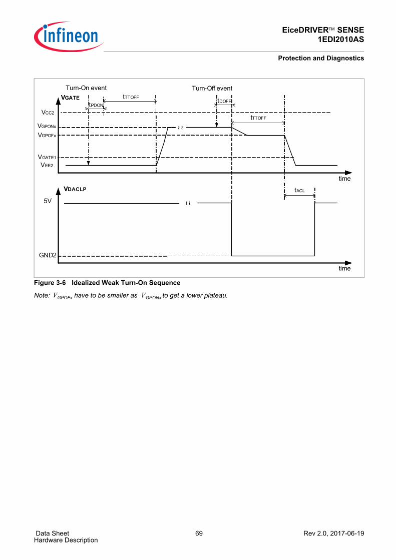
EiceDRIVER™ SENSE1EDI2010AS
Protection and Diagnostics
Data Sheet 69 Rev 2.0, 2017-06-19Hardware Description
Figure 3-6 Idealized Weak Turn-On Sequence
Note: VGPOFx have to be smaller as VGPONx to get a lower plateau.
VGATE
VEE2
VCC2
Turn-On event
tPDON
tTTOFF
time
5V
GND2
VDACLP
time
Turn-Off event
tDOFF
tTTOFF
~ ~VGPONx
~ ~tACL
VGATE1
VGPOFx
EiceDRIVER™ SENSE1EDI2010AS
Protection and Diagnostics
Data Sheet 70 Rev 2.0, 2017-06-19Hardware Description
3.5.3 Internal Clock SupervisionThe Primary Clock Supervision functionality is summarized in Table 3-8:
The clock supervision function consists on the primary clock supervision and the TCF feature.
Primary Clock SupervisionThe purpose of this supervision function is to measure the frequency the oscillator OSC1. This function works insuch a way that the PWM input signal is used to start and stop a counter clocked by OSC1. The function isactivated when the device is in OPM5 or OPM6. The counter is incremented for the duration of the High level atpin INP. At a High-to-Low transition at pin INP, the counter is stopped, and its content is transferred to bit fieldPCS.CSP. A plausibility check can therefore be made by the logic. In case of a long INP pulse, the counter doesnot overflow but stays at the maximum value until cleared. PCS.CSP is cleared by setting bit PCTRL.CLRP.The INP signal is not issued at the output stage.Note: OSC2 is indirectly monitored by the Life Sign mechanism.
Timing Calibration Feature The purpose of this function is to measure the frequency of oscillator SSOC2. The PWM input signal is used tostart and stop a counter clocked by SSOSC2. The function is activated when the device is in OPM6 (only). Thecounter is incremented for the duration of the High level at pin INP. At a High-to-Low transition at pin INP, thecounter is stopped, and its content is transferred to bit field SCS.SCSS. A plausibility check can therefore be madeby the logic. In case of a long INP pulse, the counter does not overflow but stays at the maximum value untilcleared. SCS.SCSS is cleared by a reset event or verification mode time out.The INP signal is not issued at the output stage.
Table 3-8 Primary Clock Supervision OverviewParameter Short DescriptionFunction Supervision of the frequency of OSC1 and SSOSC2.Periodicity On Request.Action in case of event N.a.Programmability No

EiceDRIVER™ SENSE1EDI2010AS
Register Description
Data Sheet 71 Rev 2.0, 2017-06-19Hardware Description
4 Register DescriptionThis chapter describes the internal registers of the device. Table 4-2 provides an overview of the implementedregisters. The abbreviations shown in Table 4-3 are used in the whole section.
Table 4-1 Register Address SpaceModule Base Address End Address NoteSPI 00H 1FH
Table 4-2 Register Overview Register Short Name
Register Long Name Offset Address
Wakeup Value
Reset Value
Register Description, Primary Register Description PID Primary ID Register 00H n.a. 4911H
PSTAT Primary Status Register 01H n.a. 0F54H
PSTAT2 Primary Second Status Register 02H n.a. 0010H
PER Primary Error Register 03H n.a. x80xH
PCFG Primary Configuration Register 04H n.a. 0004H
PCFG2 Primary Second Configuration Register 05H n.a. 0045H
PCTRL Primary Control Register 06H n.a. 001CH
PCTRL2 Primary Second Control Register 07H n.a. 0015H
PSCR Primary Supervision Function Control Register
08H n.a. 0001H
PRW Primary Read/Write Register 09H n.a. 0001H
PPIN Primary Pin Status Register 0AH n.a. 0xxxH
PCS Primary Clock Supervision Register 0BH n.a. 0001H
Register Description, Secondary Registers Description SID Secondary ID Register
10H n.a.
8921H SSTAT Secondary Status Register
11H n.a.
0001H SSTAT2 Secondary Second Status Register
12H n.a.
0xxxH SER Secondary Error Register
13H n.a.
xxxxH SCFG Secondary Configuration Register
14H n.a.
C111H SCFG2 Secondary Second Configuration Register 15H n.a. 0800H
SSCR Secondary Supervision Function Control Register
17H n.a. 0001H
SDESAT Secondary DESAT Blanking Time Register 18H n.a. 2000H
SOCP Secondary OCP Blanking Time Register 19H n.a. 0001H

EiceDRIVER™ SENSE1EDI2010AS
Register Description
Data Sheet 72 Rev 2.0, 2017-06-19Hardware Description
The registers are addressed wordwise.
SRTTOF Secondary Regular TTOFF Configuration Register
1AH n.a. 0001H
SSTTOF Secondary Safe TTOFF Configuration Register
1BH n.a. 2081H
STTON Secondary TTON Configuration Register 1CH n.a. 0001H
SADC Secondary ADC Result Register 1DH n.a. 0001H
SBC Secondary ADC Boundary Register 1EH n.a. FC01H
SCS Secondary Clock Supervision Register 1FH n.a. 0001H
Table 4-3 Bit Access Terminology Mode Symbol DescriptionBasic Access Typesread/write rw This bit or bit field can be written or read.read r This bit or bit field is read only.write w This bit or bit field is write only (read as 0H).
read/write hardware affected rwh As rw, but bit or bit field can also be modified by hardware.read hardware affected rh As r, but bit or bit field can also be modified by hardware.sticky s Bits with this attribute are “sticky” in one direction. If their reset value
is once overwritten they can be switched again into their reset state only by a reset operation. Software and internal logic (except reset-like functions) cannot switch this type of bit into its reset state by writing directly the register. The sticky attribute can be combined to other functions (e.g. ‘rh’).
Reserved / not implemented 0 Bit fields named ‘0’ indicate not implemented functions. They have the following behavior:• Reading these bit fields returns 0H.• Writing these bit fields has no effect.These bit fields are reserved. When writing, software should always set such bit fields to 0H in order to preserve compatibility with future products.
Reserved / not defined Res Certain bit fields or bit combinations in a bit field can be marked as ‘Reserved’, indicating that the behavior of the device is undefined for that combination of bits. Setting the register to such an undefined value may lead to unpredictable results. When writing, software must always set such bit fields to legal values.
Table 4-2 Register Overview (cont’d)
Register Short Name
Register Long Name Offset Address
Wakeup Value
Reset Value
EiceDRIVER™ SENSE1EDI2010AS
Register Description
Data Sheet 73 Rev 2.0, 2017-06-19Hardware Description
4.1 Primary Register Description
Primary ID RegisterThis register contains the identification number of the primary chip version.
PID Offset Wakeup Value Reset ValuePrimary ID Register
00H n.a.
4911H
Field Bits Type DescriptionPVERS 15:4 r Primary Chip Identification
This bit field defines the version of the primary chip. This bit field is hard-wired.491H a11 A11 Step.
0 3:2 r ReservedRead as 0B.
LMI 1 rh Last Message Invalid NotificationThis bit indicates if the last received SPI Message was correctly processed by the device.0B Previous Message was processed correctly.1B Previous Message was discarded.
P 0 rh Parity BitOdd Parity Bit.
15 8
7 0
15
r
PVERS
7 4
r
PVERS
3 2
r
0
11
rh
LMI
00
rh
P
EiceDRIVER™ SENSE1EDI2010AS
Register Description
Data Sheet 74 Rev 2.0, 2017-06-19Hardware Description
Primary Status RegisterThis register contains information on the status of the device.
PSTAT Offset Wakeup Value Reset ValuePrimary Status Register
01H n.a.
0F54H
Field Bits Type Description0 15:12 r Reserved
Read as 0B. ERR 11 rh Error Status
This bit is the OR combination of all bits of register PER. 0B noError No error is detected.1B error An error is detected.
GPONP 10:8 rh Gate TTON Plateau Level Configuration StatusThis bit field indicates the latest turn-on plateau level configuration request (WTO, TTON) received by the primary side via the SPI interface. Coding is identical to bit field PCTRL.GPON.
ACT 7 rh Active State Status This bit indicates if the device is in Active State (OPM4).0B notActive The device is not in Active State.1B active The device is in Active State.
SRDY 6 rh Secondary Ready StatusThis bit indicates if the secondary chip is ready for operation.0B notReady Secondary chip is not ready.1B ready Secondary chip is ready.
AVFP 5 rh ADC Result Valid FlagThis bit field indicates if a valid ADC result is available in SADC.Note: This bit field is a mirror of
SADC.AVFS
15 8
7 0
15 12
r
0
1111
rh
ERR
10 8
rh
GPONP
77
rh
ACT
66
rh
SRDY
55
rh
AVFP
4 2
rh
GPOFP
11
rh
LMI
00
rh
P
EiceDRIVER™ SENSE1EDI2010AS
Register Description
Data Sheet 75 Rev 2.0, 2017-06-19Hardware Description
GPOFP 4:2 rh Gate Regular TTOFF Plateau Level Configuration StatusThis bit field indicates the latest turn-off plateau level configuration request (regular TTOFF) received by the primary side via the SPI interface. Coding is identical to bit field PCTRL2. GPOF.
LMI 1 rh Last Message Invalid NotificationThis bit indicates if the last received SPI Message was correctly processed by the device.0B Previous Message was processed correctly.1B Previous Message was discarded.
P 0 rh Parity BitOdd Parity Bit.
Field Bits Type Description
EiceDRIVER™ SENSE1EDI2010AS
Register Description
Data Sheet 76 Rev 2.0, 2017-06-19Hardware Description
Primary Second Status RegisterThis register contains information on the status of the device.
PSTAT2 Offset Wakeup Value Reset ValuePrimary Second Status Register
02H n.a.
0010H
Field Bits Type Description0 15:12 r Reserved
Read as 0B. AXVP 11 rh ADC Under Or Overvoltage Error Status
This bit indicates if a boundary condition violation is occurring.Note: This bit is a mirror of the OR combination of bits
SADC.AUVS and SADC.AOVS
0B noError An error condition is not detected.1B error An error condition is being detected
STP 10 rh Shoot Through Protection StatusThis bit is set in case the shoot through protection inhibition time (i.e. would inhibit a PWM rising edge).0B inhibitionNotActive STP inhibition is not active.1B inhibitionActive STP inhibition is active.
FLTBP 9 rh Event Class B StatusThis bit indicates if the conditions leading to an event Class B are met.Note: This bit is a mirror of bit SSTAT.FLTBS
0B noError No error condition detected.1B error An error condition is detected.
FLTAP 8 rh Event Class A StatusThis bit indicates if the conditions leading to an event Class A are met.Note: This bit is a mirror of bit SSTAT.FLTAS
0B noError No error condition is detected.1B error An error condition is detected.
15 8
7 0
15 12
r
0
1111
rh
AXVP
1010
rh
STP
99
rh
FLTBP
88
rh
FLTAP
7 5
rh
OPMP
44
rhs
FLTB
33
rhs
FLTA
22
rh
ENVAL
11
rh
LMI
00
rh
P
EiceDRIVER™ SENSE1EDI2010AS
Register Description
Data Sheet 77 Rev 2.0, 2017-06-19Hardware Description
OPMP 7:5 rh Operating ModeThis bit field indicates which operating mode is active.Note: This bit field is a mirror of bit field
SSTAT.OPMS
000B opm0 Mode OPM0 is active . 001B opm1 Mode OPM1 is active . 010B opm2 Mode OPM2 is active.011B opm3 Mode OPM3 is active.100B opm4 Mode OPM4 is active.101B opm5 Mode OPM5 is active.110B opm6 Mode OPM6 is active.111B Reserved.
FLTB 4 rhs NFLTB Pin Driver RequestThis bit indicates what output state is driven by the device at pin NFLTB. This bit is sticky.0B tristate NFLTB is in tristate. 1B lowLevel A Low Level is issued at NFLTB.
FLTA 3 rhs NFLTA Pin Driver RequestThis bit indicates what output state is driven by the device at pin NFLTA. This bit is sticky.0B tristate NFLTA is in tristate. 1B lowLevel A Low Level issued at NFLTA.
ENVAL 2 rh EN Valid StatusThis bit indicates if the signal received on pin EN is valid. 0B notValid A non-valid signal is detected.1B valid A valid signal is detected.
LMI 1 rh Last Message Invalid NotificationThis bit indicates if the last received SPI Message was correctly processed by the device.0B Previous Message was processed correctly.1B Previous Message was discarded.
P 0 rh Parity BitOdd Parity Bit.
Field Bits Type Description

EiceDRIVER™ SENSE1EDI2010AS
Register Description
Data Sheet 78 Rev 2.0, 2017-06-19Hardware Description
Primary Error RegisterThis register provides information on the error status of the device.
PER Offset Wakeup Value Reset ValuePrimary Error Register
03H n.a.
x80xH
Field Bits Type Description0 15:13 r Reserved
Read as 0B. RSTEP 12 rhs Primary External Hard Reset flag
This bit indicates if a reset event has been detected on the primary chip due to the activation of pin NRST/RDY. This bit is sticky.0B notSet No external hard reset event has been
detected.1B set An externally hard reset event has been
detected.RSTP 11 rhs Primary Reset Flag
This bit indicates if a reset event has been detected on the primary chip. This bit is sticky.0B notSet No reset event has been detected.1B set A reset event has been detected.
ENER 10 rhs EN Signal Invalid FlagThis bit indicates if an invalid-to-valid transition on signal EN has been detected. This bit is sticky.Note: This bit can not be cleared while an error condition
is active (bit PSTAT2.ENVAL cleared).
0B notSet No event has been detected.1B set An event has been detected.
15 8
7 0
15 13
r
0
1212
rhs
RSTEP
1111
rhs
RSTP
1010
rhs
ENER
99
rhs
STPER
88
rhs
SPIER
77
rh
Res
66
rhs
ADER
5 3
r
0
22
rhs
CERP
11
rh
LMI
00
rh
P
EiceDRIVER™ SENSE1EDI2010AS
Register Description
Data Sheet 79 Rev 2.0, 2017-06-19Hardware Description
STPER 9 rhs Shoot Through Protection Error FlagThis bit indicates if a shoot through protection error event has been detected.This bit is sticky. Note: This bit can not be cleared while an error condition
is active (bit PSTAT2.STP set).
0B notSet No event has been detected.1B set An event has been detected.
SPIER 8 rhs SPI Error FlagThis indicates if an SPI error event has been detected.This bit is sticky.0B notSet No error event has been detected.1B set An error event has been detected.
Res 7 rh ReservedThis bit field is reserved.
ADER 6 rhs ADC Error FlagThis bit indicates if a boundary condition violation has occurred.This bit is sticky.Note: This bit can not be cleared while an error condition
is active (bit PSTAT2.AXVP set)
0B notSet No error condition has been detected.1B set An error condition has been detected has been
detected.0 5:3 r Reserved
Read as 0B. CERP 2 rhs Primary Communication Error Flag
This indicates if a loss of communication event 1) with the secondary chip has been detected by the primary chip. This bit is sticky.Note: This bit can not be cleared while an error condition
is active (bit PSTAT2.SRDY cleared).
0B notSet No event has been detected.1B set An event has been detected.
LMI 1 rh Last Message Invalid NotificationThis bit indicates if the last received SPI Message was correctly processed by the device.0B Previous Message was processed correctly.1B Previous Message was discarded.
P 0 rh Parity BitOdd Parity Bit.
1) This bit is not set after a reset event
Field Bits Type Description

EiceDRIVER™ SENSE1EDI2010AS
Register Description
Data Sheet 80 Rev 2.0, 2017-06-19Hardware Description
Primary Configuration RegisterThis register is used to select the configuration of the device.
PCFG Offset Wakeup Value Reset ValuePrimary Configuration Register
04H n.a.
0004H
Field Bits Type Description0 15:7 r Reserved
Read as 0B. ADTEN 6 rw ADC Trigger Input Enable
This bit enables the generation of an ADC trigger in case of a transition from Low to High at pin ADCT. 0B disabled ADCT pin is disabled. 1B enabled ADCT pin is enabled
ADAEN 5 rw NFLTA Pin Activation on Boundary Check Event EnableThis bit enables the activation of signal NFLTA in case of a transition from 0B to 1B of bit PSTAT2. AXVP. 0B disabled NFLTA activation is disabled. 1B enabled NFLTA activation is enabled
Res 4:3 rw ReservedThis bit field is reserved and shall be written with 0B.
PAREN 2 rw SPI Parity EnableThis bit indicates if the SPI parity error detection is active (reception only).0B disabled Parity Check is disabled.1B enabled Parity Check is enabled.
LMI 1 rh Last Message Invalid NotificationThis bit indicates if the last received SPI Message was correctly processed by the device.0B Previous Message was processed correctly.1B Previous Message was discarded.
P 0 rh Parity BitOdd Parity Bit.
15 8
r
0
77
r
0
66
rw
ADTEN
55
rw
ADAEN
4 3
rw
Res
22
rw
PAREN
11
rh
LMI
00
rh
P
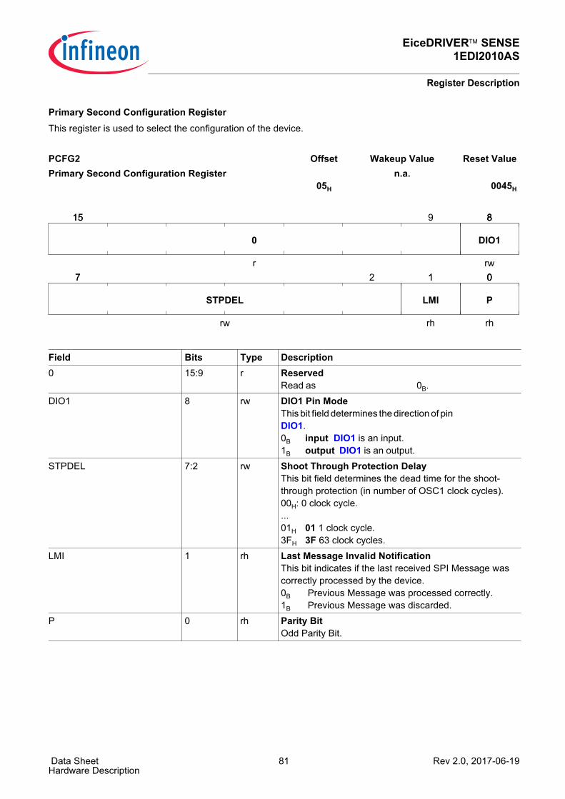
EiceDRIVER™ SENSE1EDI2010AS
Register Description
Data Sheet 81 Rev 2.0, 2017-06-19Hardware Description
Primary Second Configuration RegisterThis register is used to select the configuration of the device.
PCFG2 Offset Wakeup Value Reset ValuePrimary Second Configuration Register
05H n.a.
0045H
Field Bits Type Description0 15:9 r Reserved
Read as 0B. DIO1 8 rw DIO1 Pin Mode
This bit field determines the direction of pin DIO1. 0B input DIO1 is an input. 1B output DIO1 is an output.
STPDEL 7:2 rw Shoot Through Protection DelayThis bit field determines the dead time for the shoot-through protection (in number of OSC1 clock cycles).00H: 0 clock cycle. ...01H 01 1 clock cycle.3FH 3F 63 clock cycles.
LMI 1 rh Last Message Invalid NotificationThis bit indicates if the last received SPI Message was correctly processed by the device.0B Previous Message was processed correctly.1B Previous Message was discarded.
P 0 rh Parity BitOdd Parity Bit.
15 8
7 0
15 9
r
0
88
rw
DIO1
7 2
rw
STPDEL
11
rh
LMI
00
rh
P
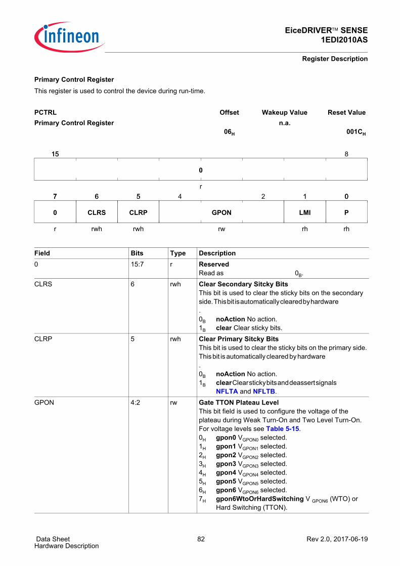
EiceDRIVER™ SENSE1EDI2010AS
Register Description
Data Sheet 82 Rev 2.0, 2017-06-19Hardware Description
Primary Control RegisterThis register is used to control the device during run-time.
PCTRL Offset Wakeup Value Reset ValuePrimary Control Register
06H n.a.
001CH
Field Bits Type Description0 15:7 r Reserved
Read as 0B. CLRS 6 rwh Clear Secondary Sitcky Bits
This bit is used to clear the sticky bits on the secondary side. This bit is automatically cleared by hardware . 0B noAction No action.1B clear Clear sticky bits.
CLRP 5 rwh Clear Primary Sitcky BitsThis bit is used to clear the sticky bits on the primary side.This bit is automatically cleared by hardware . 0B noAction No action.1B clear Clear sticky bits and deassert signals
NFLTA and NFLTB.GPON 4:2 rw Gate TTON Plateau Level
This bit field is used to configure the voltage of the plateau during Weak Turn-On and Two Level Turn-On.For voltage levels see Table 5-15.0H gpon0 VGPON0 selected. 1H gpon1 VGPON1 selected. 2H gpon2 VGPON2 selected. 3H gpon3 VGPON3 selected. 4H gpon4 VGPON4 selected. 5H gpon5 VGPON5 selected. 6H gpon6 VGPON6 selected. 7H gpon6WtoOrHardSwitching V GPON6 (WTO) or
Hard Switching (TTON).
15 8
7 0
15
r
0
77
r
0
66
rwh
CLRS
55
rwh
CLRP
4 2
rw
GPON
11
rh
LMI
00
rh
P

EiceDRIVER™ SENSE1EDI2010AS
Register Description
Data Sheet 83 Rev 2.0, 2017-06-19Hardware Description
LMI 1 rh Last Message Invalid NotificationThis bit indicates if the last received SPI Message was correctly processed by the device.0B Previous Message was processed correctly.1B Previous Message was discarded.
P 0 rh Parity BitOdd Parity Bit.
Field Bits Type Description

EiceDRIVER™ SENSE1EDI2010AS
Register Description
Data Sheet 84 Rev 2.0, 2017-06-19Hardware Description
Primary Second Control Register This register is used to control the device during run-time.
PCTRL2 Offset Wakeup Value Reset ValuePrimary Second Control Register
07H n.a.
0015H
Field Bits Type Description0 15:6 r Reserved
Read as 0B. ACRP 5 rwh ADC Conversion Request
This bit is used to trigger an ADC conversion. It can be set by a direct write or via pin ADCT. 0B none No conversion request pending.1B pending A conversion request is pending.This bit is
automatically cleared by hardwareGPOF 4:2 rw Gate Regular TTOFF Plateau Level
This bit field is used to configure the Two-Level Turn-Off plateau voltage (regular turn-off).For voltage levels see Table 5-15.0H gpof0 VGPOF0 selected. 1H gpof1 VGPOF1 selected. 2H gpof2 VGPOF2 selected. 3H gpof3 VGPOF3 selected. 4H gpof4 VGPOF4 selected. 5H gpof5 VGPOF5 selected. 6H gpof6 VGPOF6 selected. 7H gpof7 VGPOF7 selected.
LMI 1 rh Last Message Invalid NotificationThis bit indicates if the last received SPI Message was correctly processed by the device.0B Previous Message was processed correctly.1B Previous Message was discarded.
P 0 rh Parity BitOdd Parity Bit.
15 8
7 0
15
r
0
7 6
r
0
55
rwh
ACRP
4 2
rw
GPOF
11
rh
LMI
00
rh
P
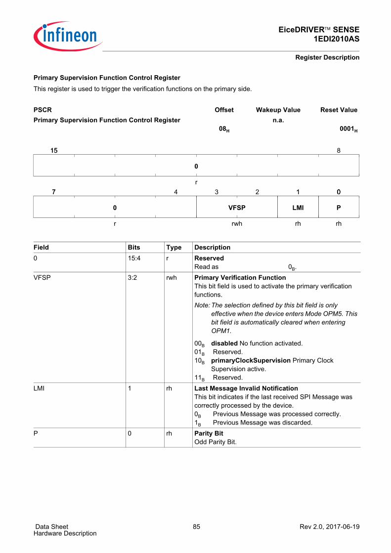
EiceDRIVER™ SENSE1EDI2010AS
Register Description
Data Sheet 85 Rev 2.0, 2017-06-19Hardware Description
Primary Supervision Function Control RegisterThis register is used to trigger the verification functions on the primary side.
PSCR Offset Wakeup Value Reset ValuePrimary Supervision Function Control Register
08H n.a.
0001H
Field Bits Type Description0 15:4 r Reserved
Read as 0B. VFSP 3:2 rwh Primary Verification Function
This bit field is used to activate the primary verification functions.Note: The selection defined by this bit field is only
effective when the device enters Mode OPM5. This bit field is automatically cleared when entering OPM1.
00B disabled No function activated.01B Reserved.10B primaryClockSupervision Primary Clock
Supervision active.11B Reserved.
LMI 1 rh Last Message Invalid NotificationThis bit indicates if the last received SPI Message was correctly processed by the device.0B Previous Message was processed correctly.1B Previous Message was discarded.
P 0 rh Parity BitOdd Parity Bit.
15 8
7 0
15
r
0
7 4
r
0
3 2
rwh
VFSP
11
rh
LMI
00
rh
P

EiceDRIVER™ SENSE1EDI2010AS
Register Description
Data Sheet 86 Rev 2.0, 2017-06-19Hardware Description
Primary Read/Write RegisterThis register provides a readable and writable address space for data integrity test during runtime. This register isnot associated with any hardware functionality.
PRW Offset Wakeup Value Reset ValuePrimary Read/Write Register
09H n.a.
0001H
Field Bits Type DescriptionRWVAL 15:2 rw Data Integrity Test Register
This bit field is “don’t care” for the device.LMI 1 rh Last Message Invalid Flag
This bit indicates if the last received SPI Message was correctly processed by the device.0B noError Previous Message processed correctly.1B error Previous Message not processed.
P 0 rh Parity BitOdd Parity Bit.
15 8
7 0
15
rw
RWVAL
7 2
rw
RWVAL
11
rh
LMI
00
rh
P
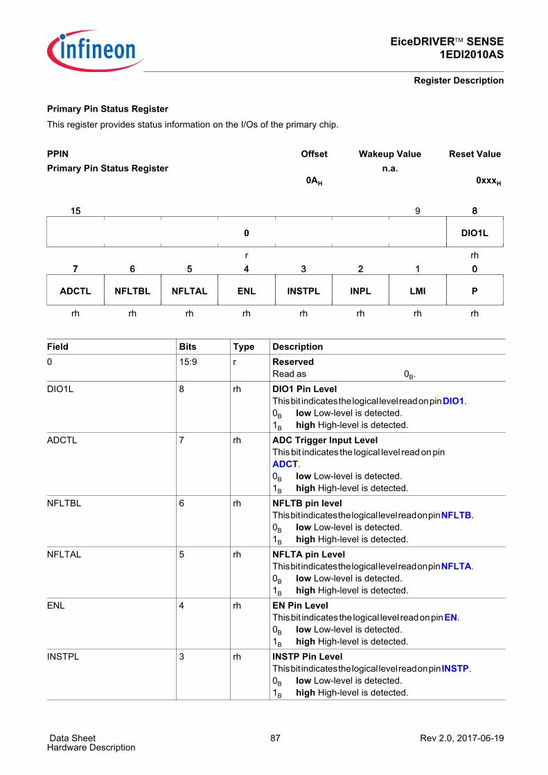
EiceDRIVER™ SENSE1EDI2010AS
Register Description
Data Sheet 87 Rev 2.0, 2017-06-19Hardware Description
Primary Pin Status RegisterThis register provides status information on the I/Os of the primary chip.
PPIN Offset Wakeup Value Reset ValuePrimary Pin Status Register
0AH n.a.
0xxxH
Field Bits Type Description0 15:9 r Reserved
Read as 0B. DIO1L 8 rh DIO1 Pin Level
This bit indicates the logical level read on pin DIO1. 0B low Low-level is detected.1B high High-level is detected.
ADCTL 7 rh ADC Trigger Input LevelThis bit indicates the logical level read on pin ADCT. 0B low Low-level is detected.1B high High-level is detected.
NFLTBL 6 rh NFLTB pin levelThis bit indicates the logical level read on pin NFLTB. 0B low Low-level is detected.1B high High-level is detected.
NFLTAL 5 rh NFLTA pin LevelThis bit indicates the logical level read on pin NFLTA. 0B low Low-level is detected.1B high High-level is detected.
ENL 4 rh EN Pin LevelThis bit indicates the logical level read on pin EN. 0B low Low-level is detected.1B high High-level is detected.
INSTPL 3 rh INSTP Pin LevelThis bit indicates the logical level read on pin INSTP. 0B low Low-level is detected.1B high High-level is detected.
15 8
7 0
15 9
r
0
88
rh
DIO1L
77
rh
ADCTL
66
rh
NFLTBL
55
rh
NFLTAL
44
rh
ENL
33
rh
INSTPL
22
rh
INPL
11
rh
LMI
00
rh
P
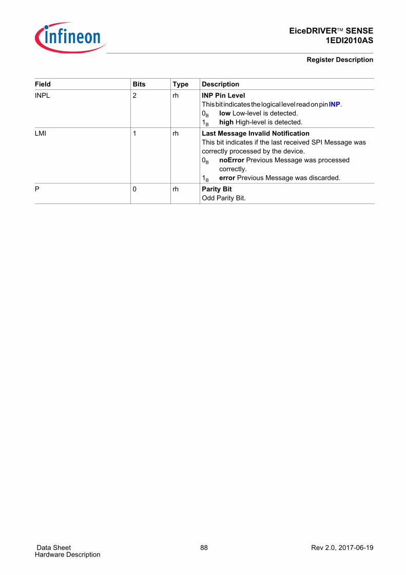
EiceDRIVER™ SENSE1EDI2010AS
Register Description
Data Sheet 88 Rev 2.0, 2017-06-19Hardware Description
INPL 2 rh INP Pin LevelThis bit indicates the logical level read on pin INP. 0B low Low-level is detected.1B high High-level is detected.
LMI 1 rh Last Message Invalid NotificationThis bit indicates if the last received SPI Message was correctly processed by the device.0B noError Previous Message was processed
correctly.1B error Previous Message was discarded.
P 0 rh Parity BitOdd Parity Bit.
Field Bits Type Description
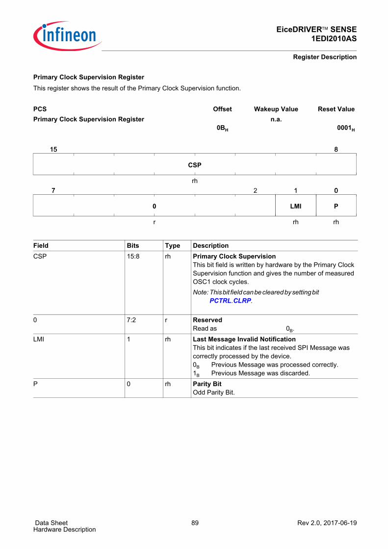
EiceDRIVER™ SENSE1EDI2010AS
Register Description
Data Sheet 89 Rev 2.0, 2017-06-19Hardware Description
Primary Clock Supervision RegisterThis register shows the result of the Primary Clock Supervision function.
PCS Offset Wakeup Value Reset ValuePrimary Clock Supervision Register
0BH n.a.
0001H
Field Bits Type DescriptionCSP 15:8 rh Primary Clock Supervision
This bit field is written by hardware by the Primary Clock Supervision function and gives the number of measured OSC1 clock cycles.Note: This bit field can be cleared by setting bit
PCTRL.CLRP.
0 7:2 r ReservedRead as 0B.
LMI 1 rh Last Message Invalid NotificationThis bit indicates if the last received SPI Message was correctly processed by the device.0B Previous Message was processed correctly.1B Previous Message was discarded.
P 0 rh Parity BitOdd Parity Bit.
15 8
7 0
15 8
rh
CSP
7 2
r
0
11
rh
LMI
00
rh
P
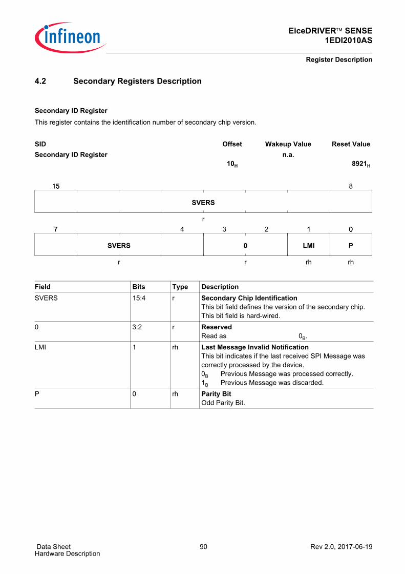
EiceDRIVER™ SENSE1EDI2010AS
Register Description
Data Sheet 90 Rev 2.0, 2017-06-19Hardware Description
4.2 Secondary Registers Description
Secondary ID RegisterThis register contains the identification number of secondary chip version.
SID Offset Wakeup Value Reset ValueSecondary ID Register
10H n.a.
8921H
Field Bits Type DescriptionSVERS 15:4 r Secondary Chip Identification
This bit field defines the version of the secondary chip. This bit field is hard-wired.
0 3:2 r ReservedRead as 0B.
LMI 1 rh Last Message Invalid NotificationThis bit indicates if the last received SPI Message was correctly processed by the device.0B Previous Message was processed correctly.1B Previous Message was discarded.
P 0 rh Parity BitOdd Parity Bit.
15 8
7 0
15
r
SVERS
7 4
r
SVERS
3 2
r
0
11
rh
LMI
00
rh
P
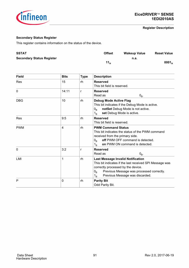
EiceDRIVER™ SENSE1EDI2010AS
Register Description
Data Sheet 91 Rev 2.0, 2017-06-19Hardware Description
Secondary Status RegisterThis register contains information on the status of the device.
SSTAT Offset Wakeup Value Reset ValueSecondary Status Register
11H n.a.
0001H
Field Bits Type DescriptionRes 15 rh Reserved
This bit field is reserved.0 14:11 r Reserved
Read as 0B. DBG 10 rh Debug Mode Active Flag
This bit indicates if the Debug Mode is active.0B notSet Debug Mode is not active.1B set Debug Mode is active.
Res 9:5 rh ReservedThis bit field is reserved.
PWM 4 rh PWM Command StatusThis bit indicates the status of the PWM command received from the primary side.0B off PWM OFF command is detected.1B on PWM ON command is detected.
0 3:2 r ReservedRead as 0B.
LMI 1 rh Last Message Invalid NotificationThis bit indicates if the last received SPI Message was correctly processed by the device.0B Previous Message was processed correctly.1B Previous Message was discarded.
P 0 rh Parity BitOdd Parity Bit.
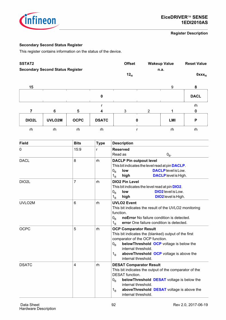
EiceDRIVER™ SENSE1EDI2010AS
Register Description
Data Sheet 92 Rev 2.0, 2017-06-19Hardware Description
Secondary Second Status RegisterThis register contains information on the status of the device.
SSTAT2 Offset Wakeup Value Reset ValueSecondary Second Status Register
12H n.a.
0xxxH
Field Bits Type Description0 15:9 r Reserved
Read as 0B. DACL 8 rh DACLP Pin outpout level
This bit indicates the level read at pin DACLP. 0B low DACLP level is Low. 1B high DACLP level is High.
DIO2L 7 rh DIO2 Pin LevelThis bit indicates the level read at pin DIO2. 0B low DIO2 level is Low. 1B high DIO2 level is High.
UVLO2M 6 rh UVLO2 EventThis bit indicates the result of the UVLO2 monitoring function.0B noError No failure condition is detected.1B error One failure condition is detected.
OCPC 5 rh OCP Comparator ResultThis bit indicates the (blanked) output of the first comparator of the OCP function.0B belowThreshold OCP voltage is below the
internal threshold. 1B aboveThreshold OCP voltage is above the
internal threshold. DSATC 4 rh DESAT Comparator Result
This bit indicates the output of the comparator of the DESAT function.0B belowThreshold DESAT voltage is below the
internal threshold. 1B aboveThreshold DESAT voltage is above the
internal threshold.
15 8
7 0
15 9
r
0
88
rh
DACL
77
rh
DIO2L
66
rh
UVLO2M
55
rh
OCPC
44
rh
DSATC
3 2
r
0
11
rh
LMI
00
rh
P
EiceDRIVER™ SENSE1EDI2010AS
Register Description
Data Sheet 93 Rev 2.0, 2017-06-19Hardware Description
0 3:2 r ReservedRead as 0B.
LMI 1 rh Last Message Invalid NotificationThis bit indicates if the last received SPI Message was correctly processed by the device.0B Previous Message was processed correctly.1B Previous Message was discarded.
P 0 rh Parity BitOdd Parity Bit.
Field Bits Type Description
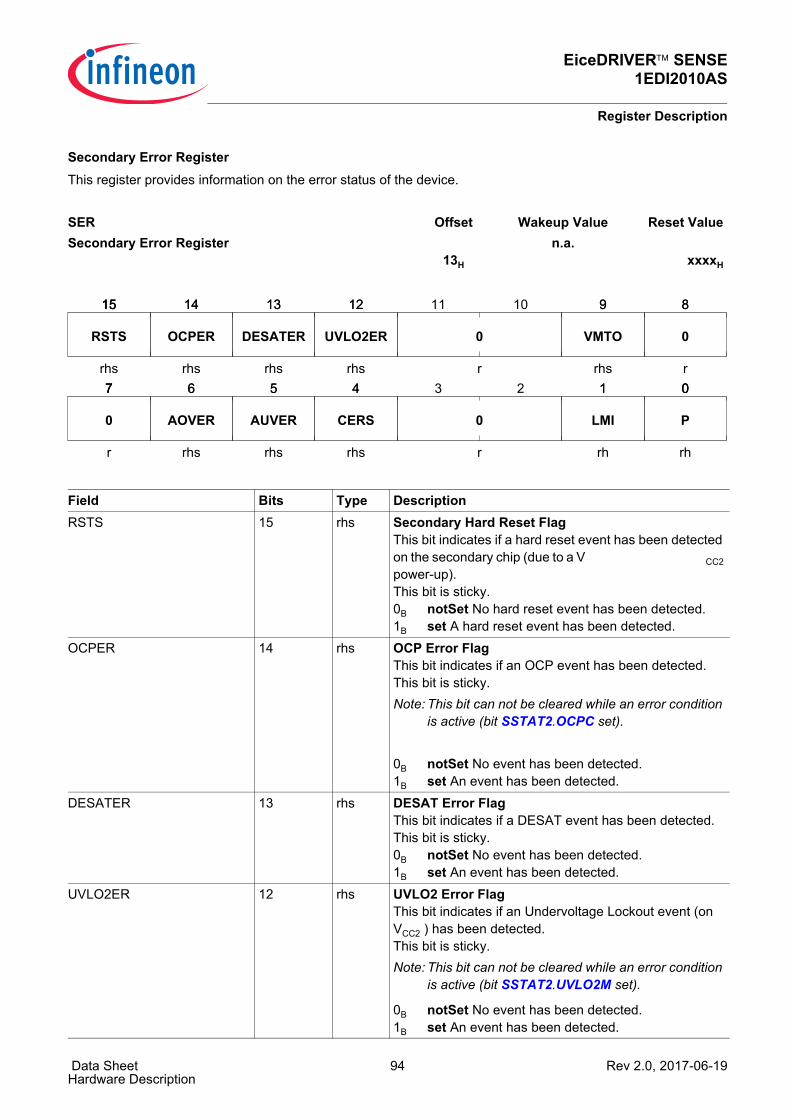
EiceDRIVER™ SENSE1EDI2010AS
Register Description
Data Sheet 94 Rev 2.0, 2017-06-19Hardware Description
Secondary Error RegisterThis register provides information on the error status of the device.
SER Offset Wakeup Value Reset ValueSecondary Error Register
13H n.a.
xxxxH
Field Bits Type DescriptionRSTS 15 rhs Secondary Hard Reset Flag
This bit indicates if a hard reset event has been detected on the secondary chip (due to a V CC2 power-up). This bit is sticky.0B notSet No hard reset event has been detected.1B set A hard reset event has been detected.
OCPER 14 rhs OCP Error FlagThis bit indicates if an OCP event has been detected.This bit is sticky.Note: This bit can not be cleared while an error condition
is active (bit SSTAT2.OCPC set).
0B notSet No event has been detected.1B set An event has been detected.
DESATER 13 rhs DESAT Error FlagThis bit indicates if a DESAT event has been detected.This bit is sticky.0B notSet No event has been detected.1B set An event has been detected.
UVLO2ER 12 rhs UVLO2 Error FlagThis bit indicates if an Undervoltage Lockout event (on VCC2 ) has been detected.This bit is sticky.Note: This bit can not be cleared while an error condition
is active (bit SSTAT2.UVLO2M set).
0B notSet No event has been detected.1B set An event has been detected.
15 8
7 0
1515
rhs
RSTS
1414
rhs
OCPER
1313
rhs
DESATER
1212
rhs
UVLO2ER
11 10
r
0
99
rhs
VMTO
8
r
0
77
r
0
66
rhs
AOVER
55
rhs
AUVER
44
rhs
CERS
3 2
r
0
11
rh
LMI
00
rh
P
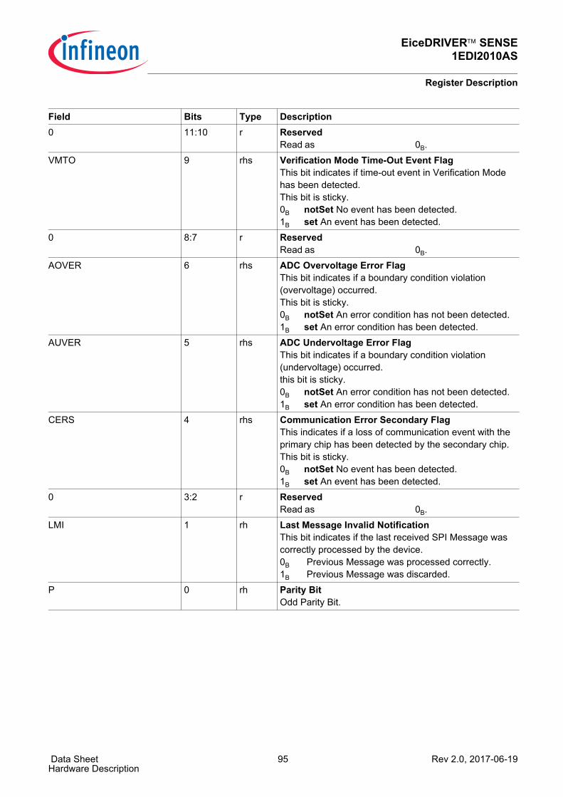
EiceDRIVER™ SENSE1EDI2010AS
Register Description
Data Sheet 95 Rev 2.0, 2017-06-19Hardware Description
0 11:10 r ReservedRead as 0B.
VMTO 9 rhs Verification Mode Time-Out Event FlagThis bit indicates if time-out event in Verification Mode has been detected.This bit is sticky.0B notSet No event has been detected.1B set An event has been detected.
0 8:7 r ReservedRead as 0B.
AOVER 6 rhs ADC Overvoltage Error FlagThis bit indicates if a boundary condition violation (overvoltage) occurred.This bit is sticky.0B notSet An error condition has not been detected.1B set An error condition has been detected.
AUVER 5 rhs ADC Undervoltage Error FlagThis bit indicates if a boundary condition violation (undervoltage) occurred.this bit is sticky.0B notSet An error condition has not been detected.1B set An error condition has been detected.
CERS 4 rhs Communication Error Secondary FlagThis indicates if a loss of communication event with the primary chip has been detected by the secondary chip.This bit is sticky.0B notSet No event has been detected.1B set An event has been detected.
0 3:2 r ReservedRead as 0B.
LMI 1 rh Last Message Invalid NotificationThis bit indicates if the last received SPI Message was correctly processed by the device.0B Previous Message was processed correctly.1B Previous Message was discarded.
P 0 rh Parity BitOdd Parity Bit.
Field Bits Type Description
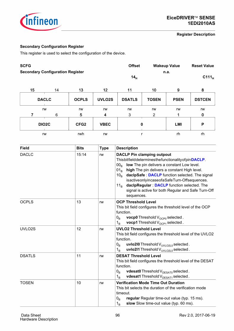
EiceDRIVER™ SENSE1EDI2010AS
Register Description
Data Sheet 96 Rev 2.0, 2017-06-19Hardware Description
Secondary Configuration RegisterThis register is used to select the configuration of the device.
SCFG Offset Wakeup Value Reset ValueSecondary Configuration Register
14H n.a.
C111H
Field Bits Type DescriptionDACLC 15:14 rw DACLP Pin clamping outpout
This bit field determines the functionality of pin DACLP. 00B low The pin delivers a constant Low level.01B high The pin delivers a constant High level.10B daclpSafe : DACLP function selected. The signal
is active only in case of a Safe Turn-Off sequences. 11B daclpRegular : DACLP function selected. The
signal is active for both Regular and Safe Turn-Off sequences.
OCPLS 13 rw OCP Threshold LevelThis bit field configures the threshold level of the OCP function.0B vocp0 Threshold VOCP0 selected . 1B vocp1 Threshold VOCP1 selected .
UVLO2S 12 rw UVLO2 Threshold LevelThis bit field configures the threshold level of the UVLO2 function.0B uvlo2l0 Threshold VUVLO2L0 selected . 1B uvlo2l1 Threshold VUVLO2L0 selected .
DSATLS 11 rw DESAT Threshold LevelThis bit field configures the threshold level of the DESAT function.0B vdesat0 Threshold VDESAT0 selected . 1B vdesat1 Threshold VDESAT1 selected .
TOSEN 10 rw Verification Mode Time Out DurationThis bit selects the duration of the verification mode timeout. 0B regular Regular time-out value (typ. 15 ms).1B slow Slow time-out value (typ. 60 ms).
15 8
7 0
15 14
rw
DACLC
1313
rw
OCPLS
1212
rw
UVLO2S
1111
rw
DSATLS
1010
rw
TOSEN
99
rw
PSEN
88
rw
DSTCEN
7 6
rw
DIO2C
55
rwh
CFG2
44
rw
VBEC
3 2
r
0
11
rh
LMI
00
rh
P
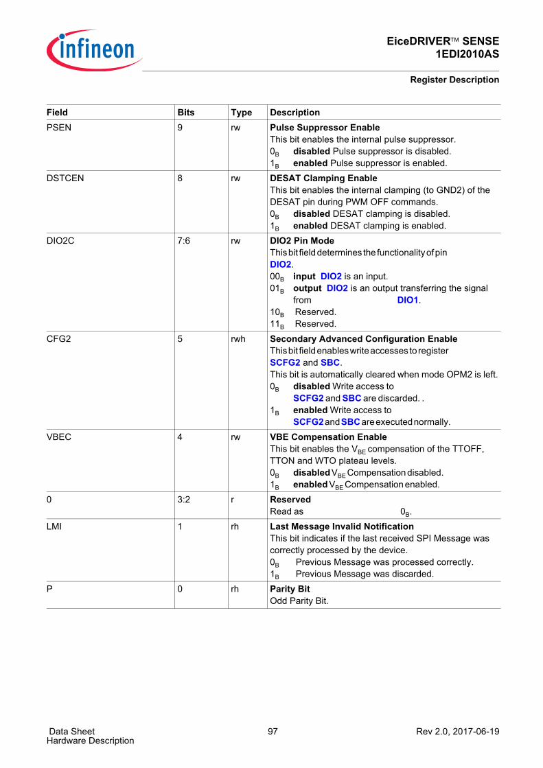
EiceDRIVER™ SENSE1EDI2010AS
Register Description
Data Sheet 97 Rev 2.0, 2017-06-19Hardware Description
PSEN 9 rw Pulse Suppressor EnableThis bit enables the internal pulse suppressor.0B disabled Pulse suppressor is disabled.1B enabled Pulse suppressor is enabled.
DSTCEN 8 rw DESAT Clamping EnableThis bit enables the internal clamping (to GND2) of the DESAT pin during PWM OFF commands.0B disabled DESAT clamping is disabled.1B enabled DESAT clamping is enabled.
DIO2C 7:6 rw DIO2 Pin ModeThis bit field determines the functionality of pin DIO2. 00B input DIO2 is an input. 01B output DIO2 is an output transferring the signal
from DIO1. 10B Reserved. 11B Reserved.
CFG2 5 rwh Secondary Advanced Configuration EnableThis bit field enables write accesses to register SCFG2 and SBC. This bit is automatically cleared when mode OPM2 is left.0B disabled Write access to
SCFG2 and SBC are discarded. . 1B enabled Write access to
SCFG2 and SBC are executed normally. VBEC 4 rw VBE Compensation Enable
This bit enables the VBE compensation of the TTOFF, TTON and WTO plateau levels. 0B disabled VBE Compensation disabled. 1B enabled VBE Compensation enabled.
0 3:2 r ReservedRead as 0B.
LMI 1 rh Last Message Invalid NotificationThis bit indicates if the last received SPI Message was correctly processed by the device.0B Previous Message was processed correctly.1B Previous Message was discarded.
P 0 rh Parity BitOdd Parity Bit.
Field Bits Type Description
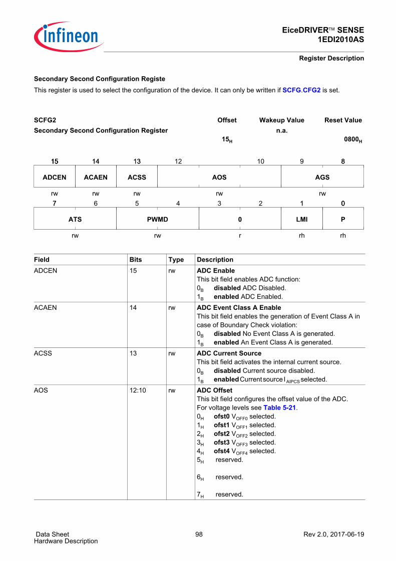
EiceDRIVER™ SENSE1EDI2010AS
Register Description
Data Sheet 98 Rev 2.0, 2017-06-19Hardware Description
Secondary Second Configuration RegisteThis register is used to select the configuration of the device. It can only be written if SCFG.CFG2 is set.
SCFG2 Offset Wakeup Value Reset ValueSecondary Second Configuration Register
15H n.a.
0800H
Field Bits Type DescriptionADCEN 15 rw ADC Enable
This bit field enables ADC function:0B disabled ADC Disabled.1B enabled ADC Enabled.
ACAEN 14 rw ADC Event Class A EnableThis bit field enables the generation of Event Class A in case of Boundary Check violation:0B disabled No Event Class A is generated.1B enabled An Event Class A is generated.
ACSS 13 rw ADC Current SourceThis bit field activates the internal current source.0B disabled Current source disabled.1B enabled Current source I AIPCS selected.
AOS 12:10 rw ADC OffsetThis bit field configures the offset value of the ADC.For voltage levels see Table 5-21.0H ofst0 VOFF0 selected. 1H ofst1 VOFF1 selected. 2H ofst2 VOFF2 selected. 3H ofst3 VOFF3 selected. 4H ofst4 VOFF4 selected. 5H reserved.
6H reserved.
7H reserved.
15 8
7 0
1515
rw
ADCEN
1414
rw
ACAEN
1313
rw
ACSS
12 10
rw
AOS
9 8
rw
AGS
7 6
rw
ATS
5 4
rw
PWMD
3 2
r
0
11
rh
LMI
00
rh
P
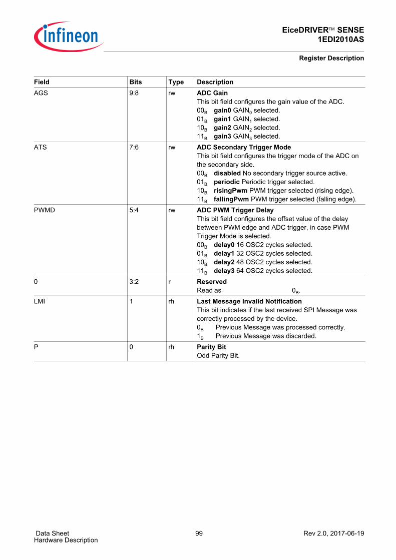
EiceDRIVER™ SENSE1EDI2010AS
Register Description
Data Sheet 99 Rev 2.0, 2017-06-19Hardware Description
AGS 9:8 rw ADC GainThis bit field configures the gain value of the ADC.00B gain0 GAIN0 selected. 01B gain1 GAIN1 selected. 10B gain2 GAIN2 selected. 11B gain3 GAIN3 selected.
ATS 7:6 rw ADC Secondary Trigger ModeThis bit field configures the trigger mode of the ADC on the secondary side.00B disabled No secondary trigger source active.01B periodic Periodic trigger selected.10B risingPwm PWM trigger selected (rising edge).11B fallingPwm PWM trigger selected (falling edge).
PWMD 5:4 rw ADC PWM Trigger DelayThis bit field configures the offset value of the delay between PWM edge and ADC trigger, in case PWM Trigger Mode is selected.00B delay0 16 OSC2 cycles selected.01B delay1 32 OSC2 cycles selected.10B delay2 48 OSC2 cycles selected.11B delay3 64 OSC2 cycles selected.
0 3:2 r ReservedRead as 0B.
LMI 1 rh Last Message Invalid NotificationThis bit indicates if the last received SPI Message was correctly processed by the device.0B Previous Message was processed correctly.1B Previous Message was discarded.
P 0 rh Parity BitOdd Parity Bit.
Field Bits Type Description
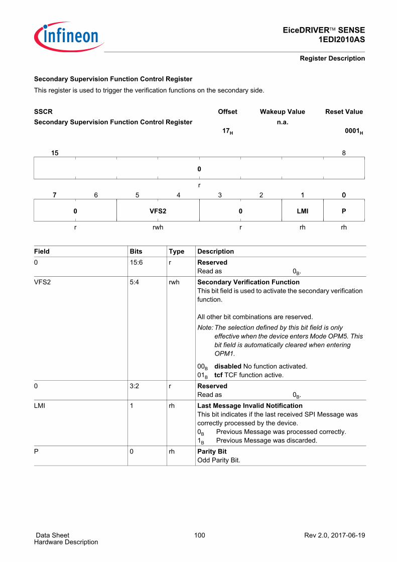
EiceDRIVER™ SENSE1EDI2010AS
Register Description
Data Sheet 100 Rev 2.0, 2017-06-19Hardware Description
Secondary Supervision Function Control RegisterThis register is used to trigger the verification functions on the secondary side.
SSCR Offset Wakeup Value Reset ValueSecondary Supervision Function Control Register
17H n.a.
0001H
Field Bits Type Description0 15:6 r Reserved
Read as 0B. VFS2 5:4 rwh Secondary Verification Function
This bit field is used to activate the secondary verification function. All other bit combinations are reserved.Note: The selection defined by this bit field is only
effective when the device enters Mode OPM5. This bit field is automatically cleared when entering OPM1.
00B disabled No function activated.01B tcf TCF function active.
0 3:2 r ReservedRead as 0B.
LMI 1 rh Last Message Invalid NotificationThis bit indicates if the last received SPI Message was correctly processed by the device.0B Previous Message was processed correctly.1B Previous Message was discarded.
P 0 rh Parity BitOdd Parity Bit.
15 8
7 0
15
r
0
7 6
r
0
5 4
rwh
VFS2
3 2
r
0
11
rh
LMI
00
rh
P
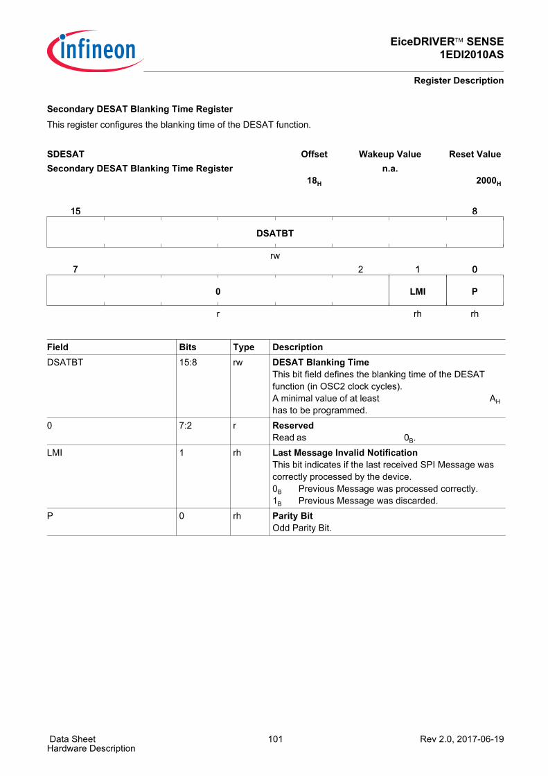
EiceDRIVER™ SENSE1EDI2010AS
Register Description
Data Sheet 101 Rev 2.0, 2017-06-19Hardware Description
Secondary DESAT Blanking Time RegisterThis register configures the blanking time of the DESAT function.
SDESAT Offset Wakeup Value Reset ValueSecondary DESAT Blanking Time Register
18H n.a.
2000H
Field Bits Type DescriptionDSATBT 15:8 rw DESAT Blanking Time
This bit field defines the blanking time of the DESAT function (in OSC2 clock cycles).A minimal value of at least AH has to be programmed.
0 7:2 r ReservedRead as 0B.
LMI 1 rh Last Message Invalid NotificationThis bit indicates if the last received SPI Message was correctly processed by the device.0B Previous Message was processed correctly.1B Previous Message was discarded.
P 0 rh Parity BitOdd Parity Bit.
15 8
7 0
15 8
rw
DSATBT
7 2
r
0
11
rh
LMI
00
rh
P
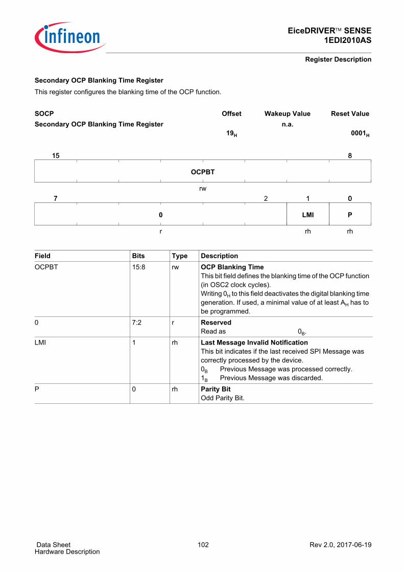
EiceDRIVER™ SENSE1EDI2010AS
Register Description
Data Sheet 102 Rev 2.0, 2017-06-19Hardware Description
Secondary OCP Blanking Time RegisterThis register configures the blanking time of the OCP function.
SOCP Offset Wakeup Value Reset ValueSecondary OCP Blanking Time Register
19H n.a.
0001H
Field Bits Type DescriptionOCPBT 15:8 rw OCP Blanking Time
This bit field defines the blanking time of the OCP function (in OSC2 clock cycles).Writing 0H to this field deactivates the digital blanking time generation. If used, a minimal value of at least AH has to be programmed.
0 7:2 r ReservedRead as 0B.
LMI 1 rh Last Message Invalid NotificationThis bit indicates if the last received SPI Message was correctly processed by the device.0B Previous Message was processed correctly.1B Previous Message was discarded.
P 0 rh Parity BitOdd Parity Bit.
15 8
7 0
15 8
rw
OCPBT
7 2
r
0
11
rh
LMI
00
rh
P
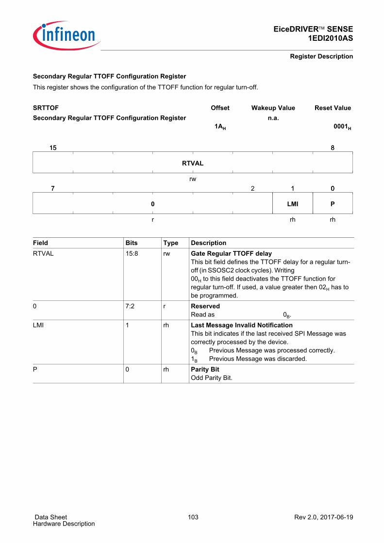
EiceDRIVER™ SENSE1EDI2010AS
Register Description
Data Sheet 103 Rev 2.0, 2017-06-19Hardware Description
Secondary Regular TTOFF Configuration RegisterThis register shows the configuration of the TTOFF function for regular turn-off.
SRTTOF Offset Wakeup Value Reset ValueSecondary Regular TTOFF Configuration Register
1AH n.a.
0001H
Field Bits Type DescriptionRTVAL 15:8 rw Gate Regular TTOFF delay
This bit field defines the TTOFF delay for a regular turn-off (in SSOSC2 clock cycles). Writing 00H to this field deactivates the TTOFF function for regular turn-off. If used, a value greater then 02H has to be programmed.
0 7:2 r ReservedRead as 0B.
LMI 1 rh Last Message Invalid NotificationThis bit indicates if the last received SPI Message was correctly processed by the device.0B Previous Message was processed correctly.1B Previous Message was discarded.
P 0 rh Parity BitOdd Parity Bit.
15 8
7 0
15 8
rw
RTVAL
7 2
r
0
11
rh
LMI
00
rh
P
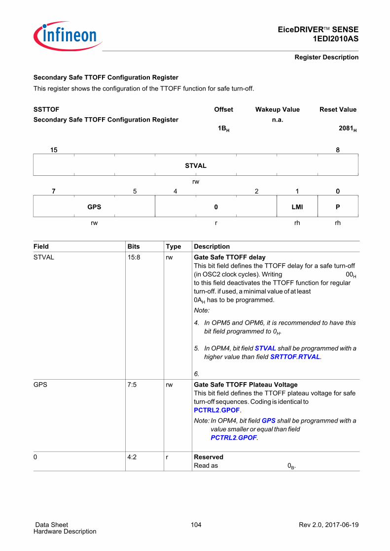
EiceDRIVER™ SENSE1EDI2010AS
Register Description
Data Sheet 104 Rev 2.0, 2017-06-19Hardware Description
Secondary Safe TTOFF Configuration RegisterThis register shows the configuration of the TTOFF function for safe turn-off.
SSTTOF Offset Wakeup Value Reset ValueSecondary Safe TTOFF Configuration Register
1BH n.a.
2081H
Field Bits Type DescriptionSTVAL 15:8 rw Gate Safe TTOFF delay
This bit field defines the TTOFF delay for a safe turn-off (in OSC2 clock cycles). Writing 00H to this field deactivates the TTOFF function for regular turn-off. if used, a minimal value of at least 0AH has to be programmed. Note:
4. In OPM5 and OPM6, it is recommended to have this bit field programmed to 0H.
5. In OPM4, bit field STVAL shall be programmed with a higher value than field SRTTOF.RTVAL.
6.
GPS 7:5 rw Gate Safe TTOFF Plateau VoltageThis bit field defines the TTOFF plateau voltage for safe turn-off sequences. Coding is identical to PCTRL2.GPOF.Note: In OPM4, bit field GPS shall be programmed with a
value smaller or equal than field PCTRL2.GPOF.
0 4:2 r ReservedRead as 0B.
15 8
7 0
15 8
rw
STVAL
7 5
rw
GPS
4 2
r
0
11
rh
LMI
00
rh
P

EiceDRIVER™ SENSE1EDI2010AS
Register Description
Data Sheet 105 Rev 2.0, 2017-06-19Hardware Description
LMI 1 rh Last Message Invalid NotificationThis bit indicates if the last received SPI Message was correctly processed by the device.0B Previous Message was processed correctly.1B Previous Message was discarded.
P 0 rh Parity BitOdd Parity Bit.
Field Bits Type Description
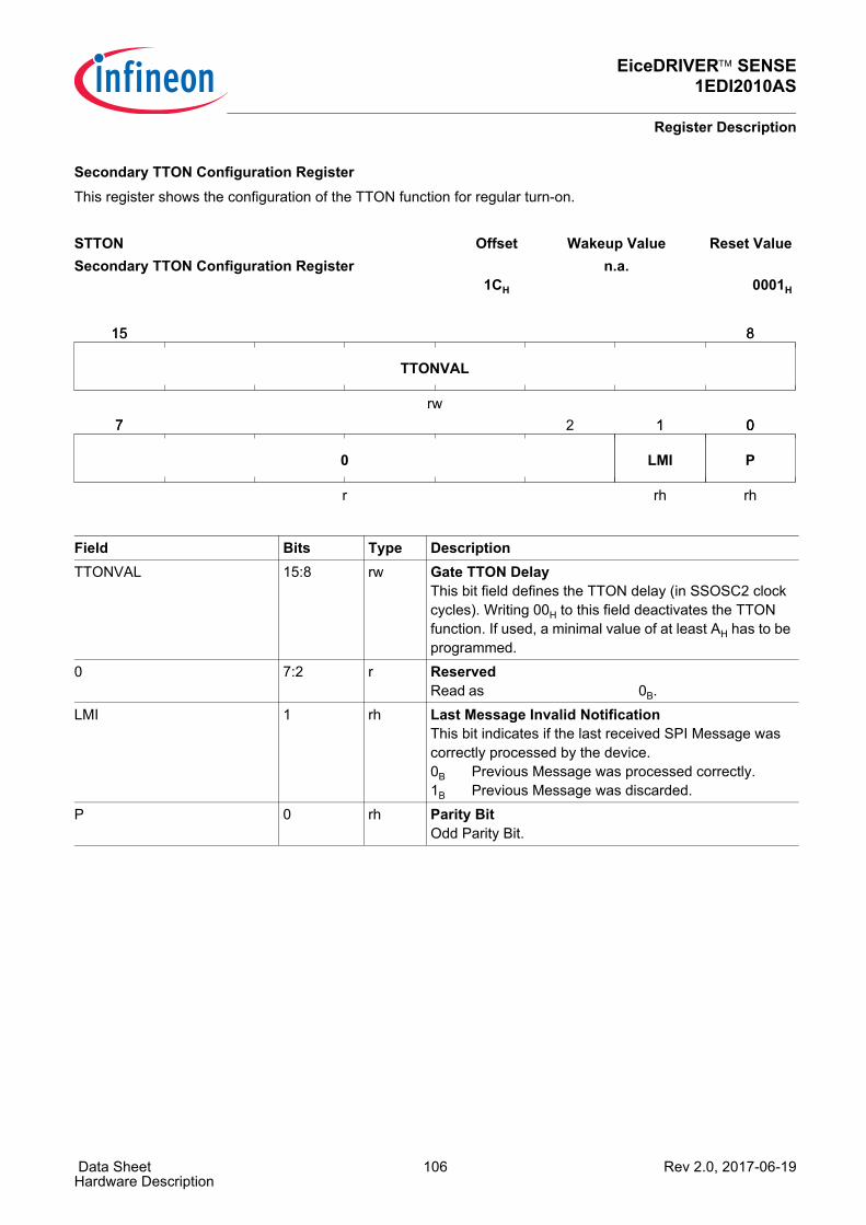
EiceDRIVER™ SENSE1EDI2010AS
Register Description
Data Sheet 106 Rev 2.0, 2017-06-19Hardware Description
Secondary TTON Configuration RegisterThis register shows the configuration of the TTON function for regular turn-on.
STTON Offset Wakeup Value Reset ValueSecondary TTON Configuration Register
1CH n.a.
0001H
Field Bits Type DescriptionTTONVAL 15:8 rw Gate TTON Delay
This bit field defines the TTON delay (in SSOSC2 clock cycles). Writing 00H to this field deactivates the TTON function. If used, a minimal value of at least AH has to be programmed.
0 7:2 r ReservedRead as 0B.
LMI 1 rh Last Message Invalid NotificationThis bit indicates if the last received SPI Message was correctly processed by the device.0B Previous Message was processed correctly.1B Previous Message was discarded.
P 0 rh Parity BitOdd Parity Bit.
15 8
7 0
15 8
rw
TTONVAL
7 2
r
0
11
rh
LMI
00
rh
P
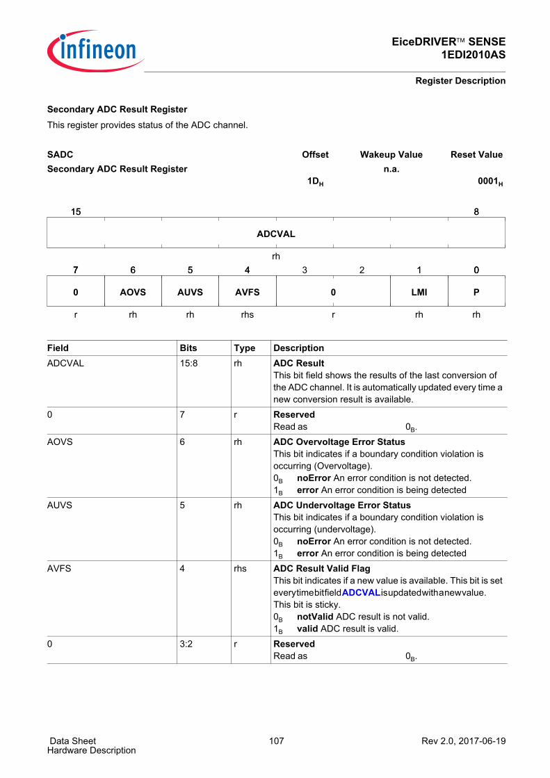
EiceDRIVER™ SENSE1EDI2010AS
Register Description
Data Sheet 107 Rev 2.0, 2017-06-19Hardware Description
Secondary ADC Result RegisterThis register provides status of the ADC channel.
SADC Offset Wakeup Value Reset ValueSecondary ADC Result Register
1DH n.a.
0001H
Field Bits Type DescriptionADCVAL 15:8 rh ADC Result
This bit field shows the results of the last conversion of the ADC channel. It is automatically updated every time a new conversion result is available.
0 7 r ReservedRead as 0B.
AOVS 6 rh ADC Overvoltage Error StatusThis bit indicates if a boundary condition violation is occurring (Overvoltage).0B noError An error condition is not detected.1B error An error condition is being detected
AUVS 5 rh ADC Undervoltage Error StatusThis bit indicates if a boundary condition violation is occurring (undervoltage).0B noError An error condition is not detected.1B error An error condition is being detected
AVFS 4 rhs ADC Result Valid FlagThis bit indicates if a new value is available. This bit is set every time bit field ADCVAL is updated with a new value. This bit is sticky.0B notValid ADC result is not valid.1B valid ADC result is valid.
0 3:2 r ReservedRead as 0B.
15 8
7 0
15 8
rh
ADCVAL
77
r
0
66
rh
AOVS
55
rh
AUVS
44
rhs
AVFS
3 2
r
0
11
rh
LMI
00
rh
P

EiceDRIVER™ SENSE1EDI2010AS
Register Description
Data Sheet 108 Rev 2.0, 2017-06-19Hardware Description
LMI 1 rh Last Message Invalid NotificationThis bit indicates if the last received SPI Message was correctly processed by the device.0B Previous Message was processed correctly.1B Previous Message was discarded.
P 0 rh Parity BitOdd Parity Bit.
Field Bits Type Description
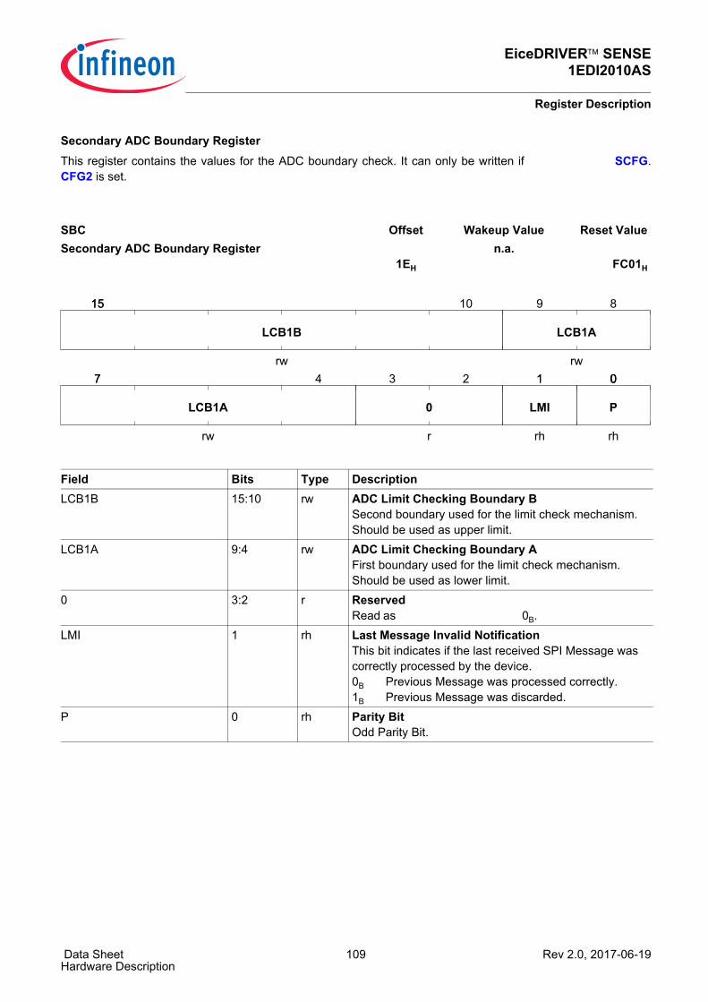
EiceDRIVER™ SENSE1EDI2010AS
Register Description
Data Sheet 109 Rev 2.0, 2017-06-19Hardware Description
Secondary ADC Boundary RegisterThis register contains the values for the ADC boundary check. It can only be written if SCFG.CFG2 is set.
SBC Offset Wakeup Value Reset ValueSecondary ADC Boundary Register
1EH n.a.
FC01H
Field Bits Type DescriptionLCB1B 15:10 rw ADC Limit Checking Boundary B
Second boundary used for the limit check mechanism. Should be used as upper limit.
LCB1A 9:4 rw ADC Limit Checking Boundary AFirst boundary used for the limit check mechanism. Should be used as lower limit.
0 3:2 r ReservedRead as 0B.
LMI 1 rh Last Message Invalid NotificationThis bit indicates if the last received SPI Message was correctly processed by the device.0B Previous Message was processed correctly.1B Previous Message was discarded.
P 0 rh Parity BitOdd Parity Bit.
15 8
7 0
15 10
rw
LCB1B
9
rw
LCB1A
7 4
rw
LCB1A
3 2
r
0
11
rh
LMI
00
rh
P

EiceDRIVER™ SENSE1EDI2010AS
Register Description
Data Sheet 110 Rev 2.0, 2017-06-19Hardware Description
Secondary Clock Supervision Register This register is for internal purpose only.
SCS Offset Wakeup Value Reset ValueSecondary Clock Supervision Register
1FH n.a.
0001H
Field Bits Type DescriptionSCSS 15:8 rh Secondary Supervision Oscillator Clock Cycles
This bit field is written by hardware by the TCF function and gives the number of measured Start Stop Oscillator clock cycles.
0 7:2 r ReservedRead as 0B.
LMI 1 rh Last Message Invalid NotificationThis bit indicates if the last received SPI Message was correctly processed by the device.0B Previous Message was processed correctly.1B Previous Message was discarded.
P 0 rh Parity BitOdd Parity Bit.
15 8
7 0
15 8
rh
SCSS
7 2
r
0
11
rh
LMI
00
rh
P
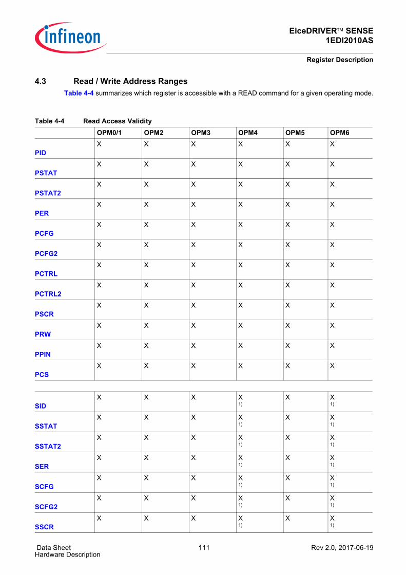
EiceDRIVER™ SENSE1EDI2010AS
Register Description
Data Sheet 111 Rev 2.0, 2017-06-19Hardware Description
4.3 Read / Write Address Ranges Table 4-4 summarizes which register is accessible with a READ command for a given operating mode.
Table 4-4 Read Access ValidityOPM0/1 OPM2 OPM3 OPM4 OPM5 OPM6
PID
X X X X X X
PSTAT
X X X X X X
PSTAT2
X X X X X X
PER
X X X X X X
PCFG
X X X X X X
PCFG2
X X X X X X
PCTRL
X X X X X X
PCTRL2
X X X X X X
PSCR
X X X X X X
PRW
X X X X X X
PPIN
X X X X X X
PCS
X X X X X X
SID
X X X X 1)
X X 1)
SSTAT
X X X X 1)
X X 1)
SSTAT2
X X X X 1)
X X 1)
SER
X X X X 1)
X X 1)
SCFG
X X X X 1)
X X 1)
SCFG2
X X X X 1)
X X 1)
SSCR
X X X X 1)
X X 1)
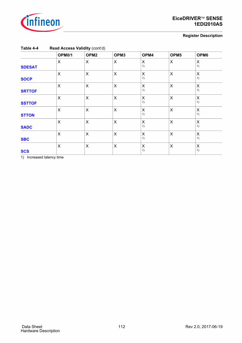
EiceDRIVER™ SENSE1EDI2010AS
Register Description
Data Sheet 112 Rev 2.0, 2017-06-19Hardware Description
SDESAT
X X X X 1)
X X 1)
SOCP
X X X X 1)
X X 1)
SRTTOF
X X X X 1)
X X 1)
SSTTOF
X X X X 1)
X X 1)
STTON
X X X X 1)
X X 1)
SADC
X X X X 1)
X X 1)
SBC
X X X X 1)
X X 1)
SCS
X X X X 1)
X X 1)
1) Increased latency time
Table 4-4 Read Access Validity (cont’d)
OPM0/1 OPM2 OPM3 OPM4 OPM5 OPM6
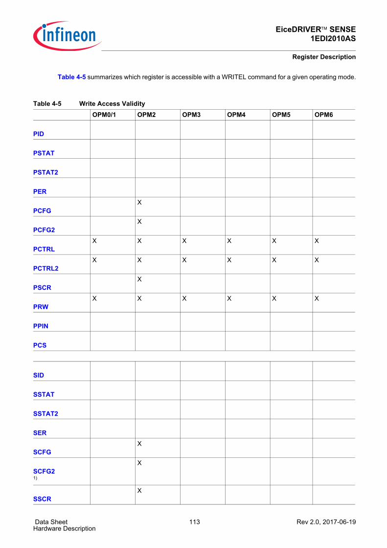
EiceDRIVER™ SENSE1EDI2010AS
Register Description
Data Sheet 113 Rev 2.0, 2017-06-19Hardware Description
Table 4-5 summarizes which register is accessible with a WRITEL command for a given operating mode.
Table 4-5 Write Access ValidityOPM0/1 OPM2 OPM3 OPM4 OPM5 OPM6
PID
PSTAT
PSTAT2
PER
PCFG
X
PCFG2
X
PCTRL
X X X X X X
PCTRL2
X X X X X X
PSCR
X
PRW
X X X X X X
PPIN
PCS
SID
SSTAT
SSTAT2
SER
SCFG
X
SCFG2 1)
X
SSCR
X
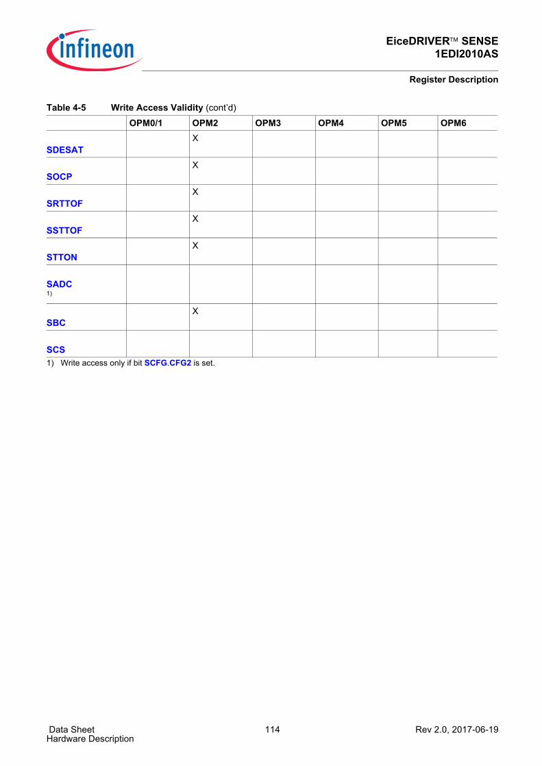
EiceDRIVER™ SENSE1EDI2010AS
Register Description
Data Sheet 114 Rev 2.0, 2017-06-19Hardware Description
SDESAT
X
SOCP
X
SRTTOF
X
SSTTOF
X
STTON
X
SADC 1)
SBC
X
SCS
1) Write access only if bit SCFG.CFG2 is set.
Table 4-5 Write Access Validity (cont’d)
OPM0/1 OPM2 OPM3 OPM4 OPM5 OPM6
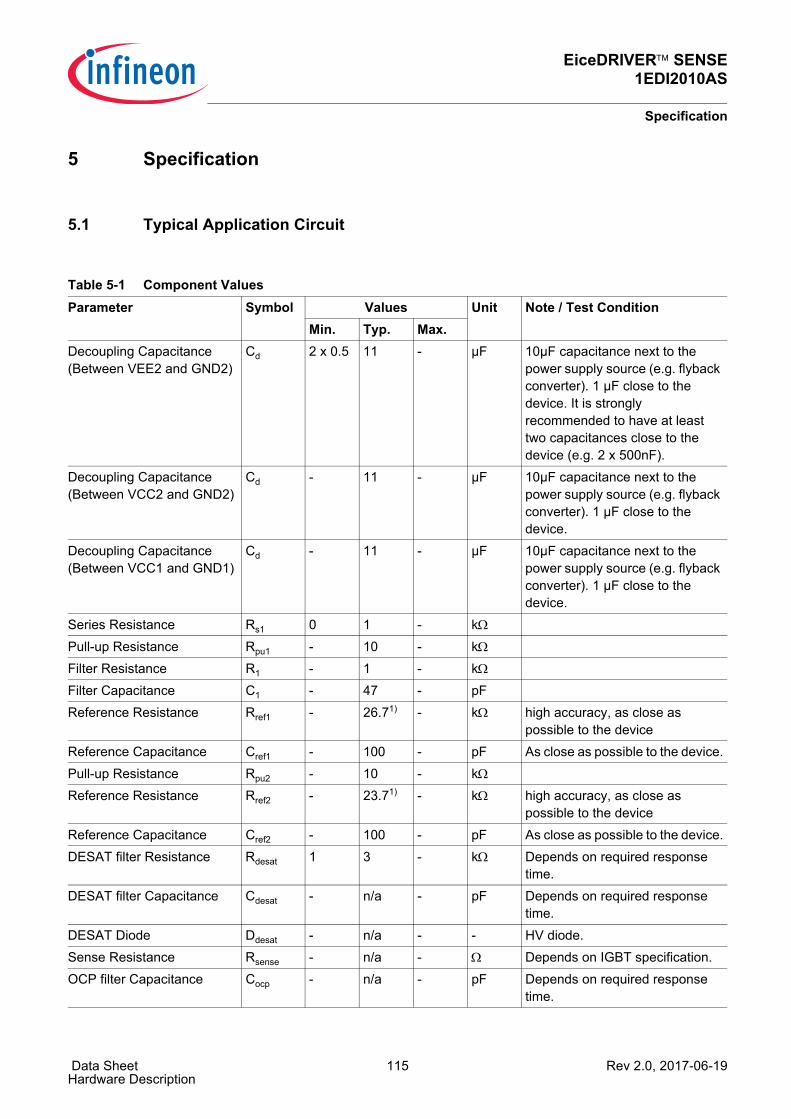
EiceDRIVER™ SENSE1EDI2010AS
Specification
Data Sheet 115 Rev 2.0, 2017-06-19Hardware Description
5 Specification
5.1 Typical Application Circuit
Table 5-1 Component ValuesParameter Symbol Values Unit Note / Test Condition
Min. Typ. Max.Decoupling Capacitance (Between VEE2 and GND2)
Cd 2 x 0.5 11 - µF 10µF capacitance next to the power supply source (e.g. flyback converter). 1 µF close to the device. It is strongly recommended to have at least two capacitances close to the device (e.g. 2 x 500nF).
Decoupling Capacitance (Between VCC2 and GND2)
Cd - 11 - µF 10µF capacitance next to the power supply source (e.g. flyback converter). 1 µF close to the device.
Decoupling Capacitance (Between VCC1 and GND1)
Cd - 11 - µF 10µF capacitance next to the power supply source (e.g. flyback converter). 1 µF close to the device.
Series Resistance Rs1 0 1 - kΩPull-up Resistance Rpu1 - 10 - kΩFilter Resistance R1 - 1 - kΩFilter Capacitance C1 - 47 - pFReference Resistance Rref1 - 26.71) - kΩ high accuracy, as close as
possible to the deviceReference Capacitance Cref1 - 100 - pF As close as possible to the device.Pull-up Resistance Rpu2 - 10 - kΩReference Resistance Rref2 - 23.71) - kΩ high accuracy, as close as
possible to the deviceReference Capacitance Cref2 - 100 - pF As close as possible to the device.DESAT filter Resistance Rdesat 1 3 - kΩ Depends on required response
time.DESAT filter Capacitance Cdesat - n/a - pF Depends on required response
time.DESAT Diode Ddesat - n/a - - HV diode.Sense Resistance Rsense - n/a - Ω Depends on IGBT specification.OCP filter Capacitance Cocp - n/a - pF Depends on required response
time.
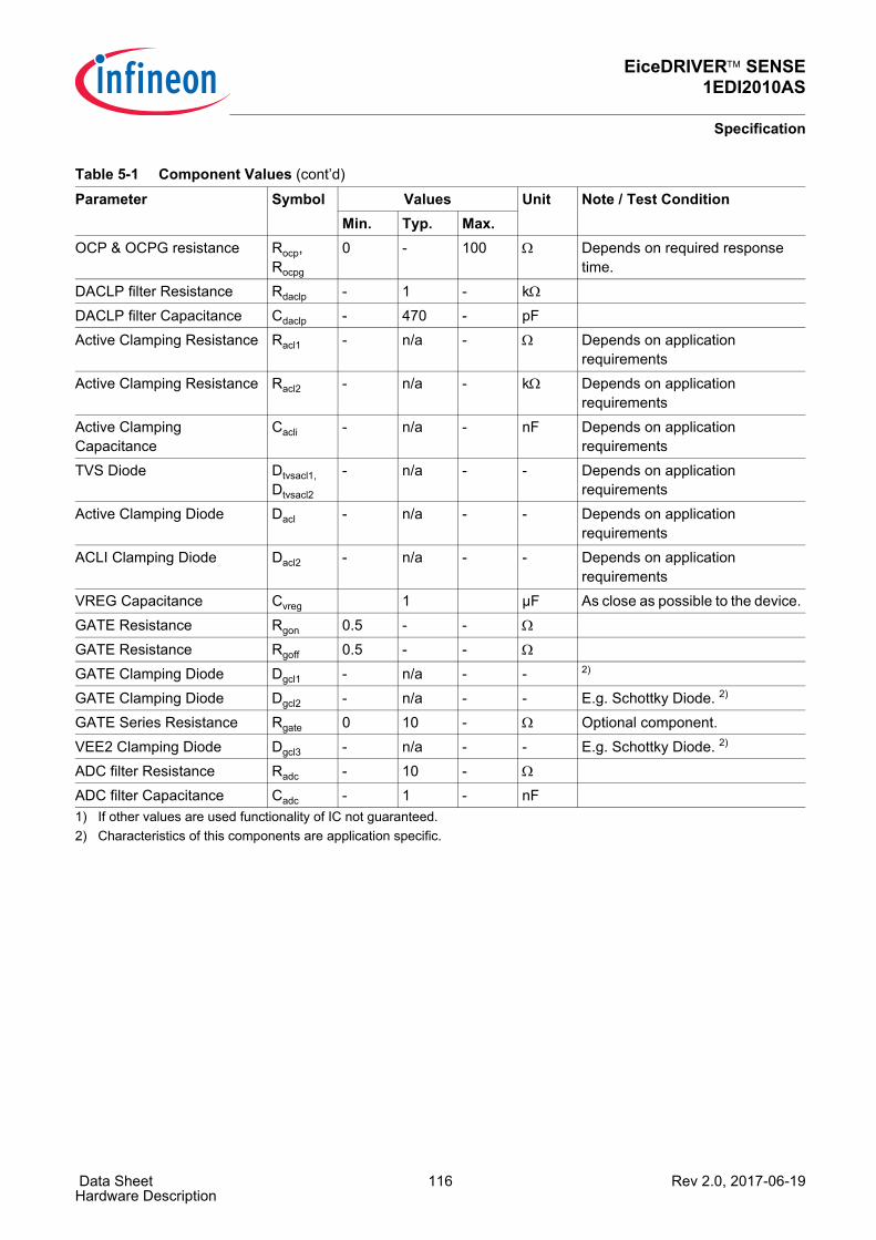
EiceDRIVER™ SENSE1EDI2010AS
Specification
Data Sheet 116 Rev 2.0, 2017-06-19Hardware Description
OCP & OCPG resistance Rocp,Rocpg
0 - 100 Ω Depends on required response time.
DACLP filter Resistance Rdaclp - 1 - kΩDACLP filter Capacitance Cdaclp - 470 - pFActive Clamping Resistance Racl1 - n/a - Ω Depends on application
requirementsActive Clamping Resistance Racl2 - n/a - kΩ Depends on application
requirementsActive Clamping Capacitance
Cacli - n/a - nF Depends on application requirements
TVS Diode Dtvsacl1, Dtvsacl2
- n/a - - Depends on application requirements
Active Clamping Diode Dacl - n/a - - Depends on application requirements
ACLI Clamping Diode Dacl2 - n/a - - Depends on application requirements
VREG Capacitance Cvreg 1 µF As close as possible to the device.GATE Resistance Rgon 0.5 - - Ω
GATE Resistance Rgoff 0.5 - - Ω
GATE Clamping Diode Dgcl1 - n/a - - 2)
GATE Clamping Diode Dgcl2 - n/a - - E.g. Schottky Diode. 2)
GATE Series Resistance Rgate 0 10 - Ω Optional component.VEE2 Clamping Diode Dgcl3 - n/a - - E.g. Schottky Diode. 2)
ADC filter Resistance Radc - 10 - Ω
ADC filter Capacitance Cadc - 1 - nF1) If other values are used functionality of IC not guaranteed.2) Characteristics of this components are application specific.
Table 5-1 Component Values (cont’d)
Parameter Symbol Values Unit Note / Test ConditionMin. Typ. Max.
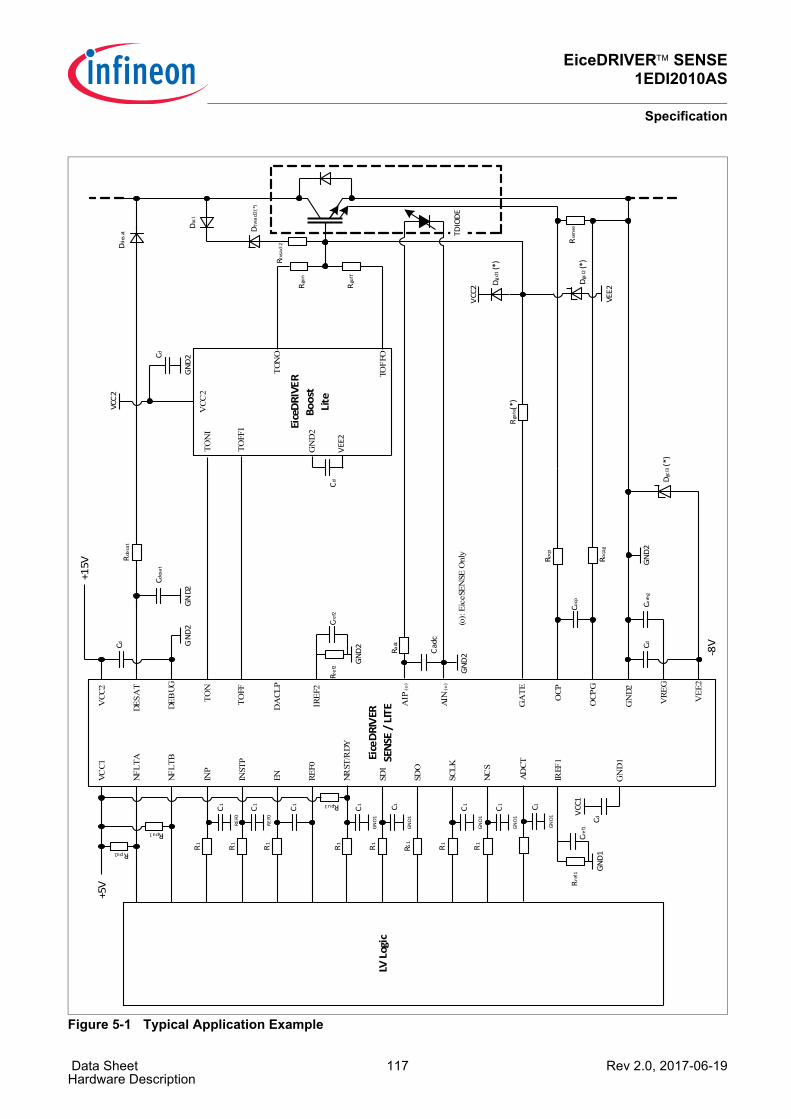
EiceDRIVER™ SENSE1EDI2010AS
Specification
Data Sheet 117 Rev 2.0, 2017-06-19Hardware Description
Figure 5-1 Typical Application Example
INP
INST
P
IREF
1
REF0
EN NRST
/RDY
NFLT
A
NFLT
B
SDI
SDO
NCS
SCLK
AIN
(o)
TON
TOFF
DESA
T
OCP
DEB
UG
AIP
(o)
DA
CLP
TON
I
TON
O
TOFF
O
Rgo
n
Rgo
ff
Rdes
at
Cdes
at
GN
D2
Rocp
Cocp
Rse
nse
GA
TE
TOFF
I
GN
D2
LV L
ogic
Eice
DRI
VER
Boos
tLi
te
R1
REF0
R1
R1
GN
D1Rpu1
Rpu1
Rre
f1
Ddes
at
Dac
l
VEE
2
GN
D2
Cd
-8V
VCC
2
+15V
Cd
VCC1
+5V
R1
RS1
R1
R1
GN
D1
Cd
VCC
2
Eice
DRI
VER
SEN
SE /
LIT
E
VCC
2
VCC
2
GN
D2
VEE
2
Dgc
l1 (*
)
C1
VRE
G
Cvre
g
IREF
2
C1
REF0
C1
R1
GND1
C1
GND1
GND1
GND1
VEE2
Dgc
l2 (*
)
Cd
GN
D2Cd
VCC
1
OCP
G
C 1 C1
C1Rpu1
GN
D2
Cref
1
GN
D2
R ref
2Cr
ef2
Radc
Cad
c
GN
D2
Dgc
l3(*
)
Rga
te(*
)
Rocp
g
Dtv
sacl2
(*)
ADCT
GND1
C1
TDIO
DE(o
): Ei
ceSE
NSE
Onl
y
Rtvs
acl2
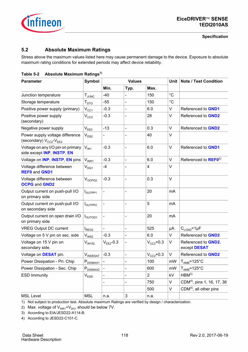
EiceDRIVER™ SENSE1EDI2010AS
Specification
Data Sheet 118 Rev 2.0, 2017-06-19Hardware Description
5.2 Absolute Maximum RatingsStress above the maximum values listed here may cause permanent damage to the device. Exposure to absolutemaximum rating conditions for extended periods may affect device reliability.
Table 5-2 Absolute Maximum Ratings1)
1) Not subject to production test. Absolute maximum Ratings are verified by design / characterization.
Parameter Symbol Values Unit Note / Test ConditionMin. Typ. Max.
Junction temperature TJUNC -40 - 150 °CStorage temperature TSTO -55 - 150 °CPositive power supply (primary) VCC1 -0.3 - 6.0 V Referenced to GND1Positive power supply (secondary)
VCC2 -0.3 - 28 V Referenced to GND2
Negative power supply VEE2 -13 - 0.3 V Referenced to GND2Power supply voltage difference (secondary) VCC2-VEE2
VDS2 - - 40 V
Voltage on any I/O pin on primary side except INP, INSTP, EN
VIN1 -0.3 - 6.0 V Referenced to GND1
Voltage on INP, INSTP, EN pins VINR1 -0.3 - 6.0 V Referenced to REF02)
2) Max. voltage of VINR1+VDG1 should be below 7V.
Voltage difference between REF0 and GND1
VDG1 -4 - 4 V
Voltage difference between OCPG and GND2
VOCPG2 -0.3 - 0.3 V
Output current on push-pull I/O on primary side
IOUTPP1 - - 20 mA
Output current on push-pull I/O on secondary side
IOUTPP2 - - 5 mA
Output current on open drain I/O on primary side
IOUTOD1 - - 20 mA
VREG Output DC current IREG2 - - 525 µA CLOAD=1µFVoltage on 5 V pin on sec. side VIN52 -0.3 - 6.0 V Referenced to GND2Voltage on 15 V pin on secondary side.
VIN152 VEE2-0.3 - VCC2+0.3 V Referenced to GND2, except DESAT
Voltage on DESAT pin. VINDESAT -0.3 - VCC2+0.3 V Referenced to GND2Power Dissipation - Pri. Chip PDISMAX1 - - 100 mW TAMB=125°CPower Dissipation - Sec. Chip PDISMAX2 - - 600 mW TAMB=125°CESD Immunity VESD - - 2 kV HBM3)
3) According to EIA/JESD22-A114-B.
- - 750 V CDM4), pins 1, 16, 17, 36
4) According to JESD22-C101-C.
500 V CDM4), all other pinsMSL Level MSL n.a. 3 n.a.

EiceDRIVER™ SENSE1EDI2010AS
Specification
Data Sheet 119 Rev 2.0, 2017-06-19Hardware Description
5.3 Operating rangeThe following operating conditions must not be exceeded in order to ensure correct operation of the 1EDI2010AS.All parameters specified in the following sections refer to these operating conditions, unless otherwise noticed.
5.4 Thermal CharacteristicsThe indicated thermal parameters apply to the full operating range, unless otherwise specified.
Table 5-3 Operating ConditionsParameter Symbol Values Unit Note / Test Condition
Min. Typ. Max.Ambient temperature Tamb -40 - 125 °CPositive power supply (primary) VCC1 4.65 5.0 5.5 V Referenced to GND11)
1) Deterministic and correct operation of the device is guaranteed down to VUVLO1L.
Positive power supply (secondary) VCC2 13.0 15.0 18.0 V Referenced to GND22)
2) Deterministic and correct operation of the device is guaranteed down to VUVLO2L.
Negative power supply VEE2 -10.0 -8.0 0 V Referenced to GND23)
3) Deterministic and correct operation of the device is guaranteed up to 0.3V.
PWM switching frequency fsw - - 30 kHz 4)
4) Maximum junction temperature of the device must not be exceeded.
Common Mode Transient Immunity dVISO/dt -100 - 100 kV/μs At 1000 V5)
5) Not subject to production test. This parameter is verified by design / characterization.
Pulsed Magnetic Field Transient Immunity
HISO -1000 1000 A/m tr=10s 5)6)
6) As per IEC 61000-4-9
Table 5-4 Thermal CharacteristicsParameter Symbol Values Unit Note / Test Condition
Min. Typ. Max.Thermal Resistance Junction to Ambient
RTHJA - 60 - K/W Tamb=125°C1)2)
1) Not subject to production test. This parameter is verified by design / characterization.2) The thermal characteristics are done with a 6 layers board with the dimension 30mm x 40mm x 1.5mm and a cu-thickness
of 35µm each layer (cooling areas should be foreseen on top and bottom, but shouldn’t cover the isolation area of the IC).
Thermal Resistance Junction to Case RTHJC - - 41 K/W Tamb=125°C1)
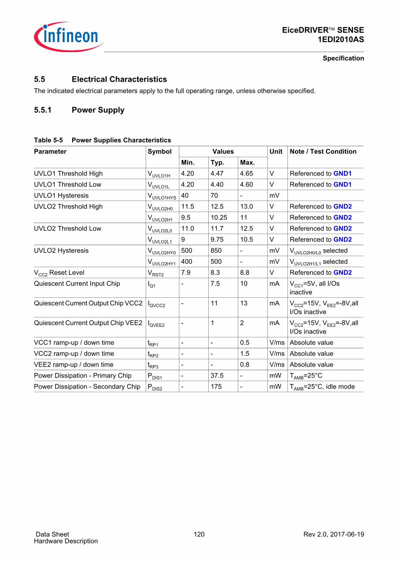
EiceDRIVER™ SENSE1EDI2010AS
Specification
Data Sheet 120 Rev 2.0, 2017-06-19Hardware Description
5.5 Electrical CharacteristicsThe indicated electrical parameters apply to the full operating range, unless otherwise specified.
5.5.1 Power Supply
Table 5-5 Power Supplies CharacteristicsParameter Symbol Values Unit Note / Test Condition
Min. Typ. Max.UVLO1 Threshold High VUVLO1H 4.20 4.47 4.65 V Referenced to GND1UVLO1 Threshold Low VUVLO1L 4.20 4.40 4.60 V Referenced to GND1UVLO1 Hysteresis VUVLO1HYS 40 70 - mVUVLO2 Threshold High VUVLO2H0 11.5 12.5 13.0 V Referenced to GND2
VUVLO2H1 9.5 10.25 11 V Referenced to GND2UVLO2 Threshold Low VUVLO2L0 11.0 11.7 12.5 V Referenced to GND2
VUVLO2L1 9 9.75 10.5 V Referenced to GND2UVLO2 Hysteresis VUVLO2HY0 500 850 - mV VUVLO2H0/L0 selected
VUVLO2HY1 400 500 - mV VUVLO2H1/L1 selectedVCC2 Reset Level VRST2 7.9 8.3 8.8 V Referenced to GND2Quiescent Current Input Chip IQ1 - 7.5 10 mA VCC1=5V, all I/Os
inactiveQuiescent Current Output Chip VCC2 IQVCC2 - 11 13 mA VCC2=15V, VEE2=-8V,all
I/Os inactiveQuiescent Current Output Chip VEE2 IQVEE2 - 1 2 mA VCC2=15V, VEE2=-8V,all
I/Os inactiveVCC1 ramp-up / down time tRP1 - - 0.5 V/ms Absolute valueVCC2 ramp-up / down time tRP2 - - 1.5 V/ms Absolute valueVEE2 ramp-up / down time tRP3 - - 0.8 V/ms Absolute valuePower Dissipation - Primary Chip PDIS1 - 37.5 - mW TAMB=25°CPower Dissipation - Secondary Chip PDIS2 - 175 - mW TAMB=25°C, idle mode
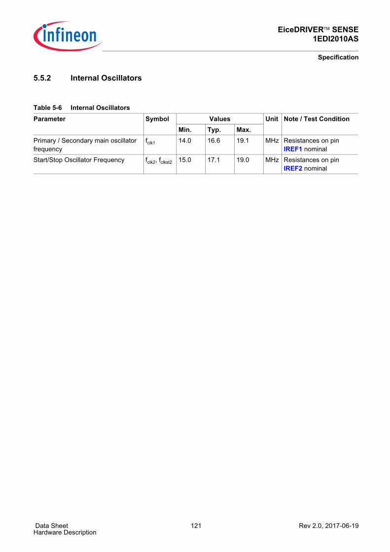
EiceDRIVER™ SENSE1EDI2010AS
Specification
Data Sheet 121 Rev 2.0, 2017-06-19Hardware Description
5.5.2 Internal Oscillators
Table 5-6 Internal OscillatorsParameter Symbol Values Unit Note / Test Condition
Min. Typ. Max.Primary / Secondary main oscillator frequency
fclk1 14.0 16.6 19.1 MHz Resistances on pin IREF1 nominal
Start/Stop Oscillator Frequency fclk2, fclkst2 15.0 17.1 19.0 MHz Resistances on pin IREF2 nominal
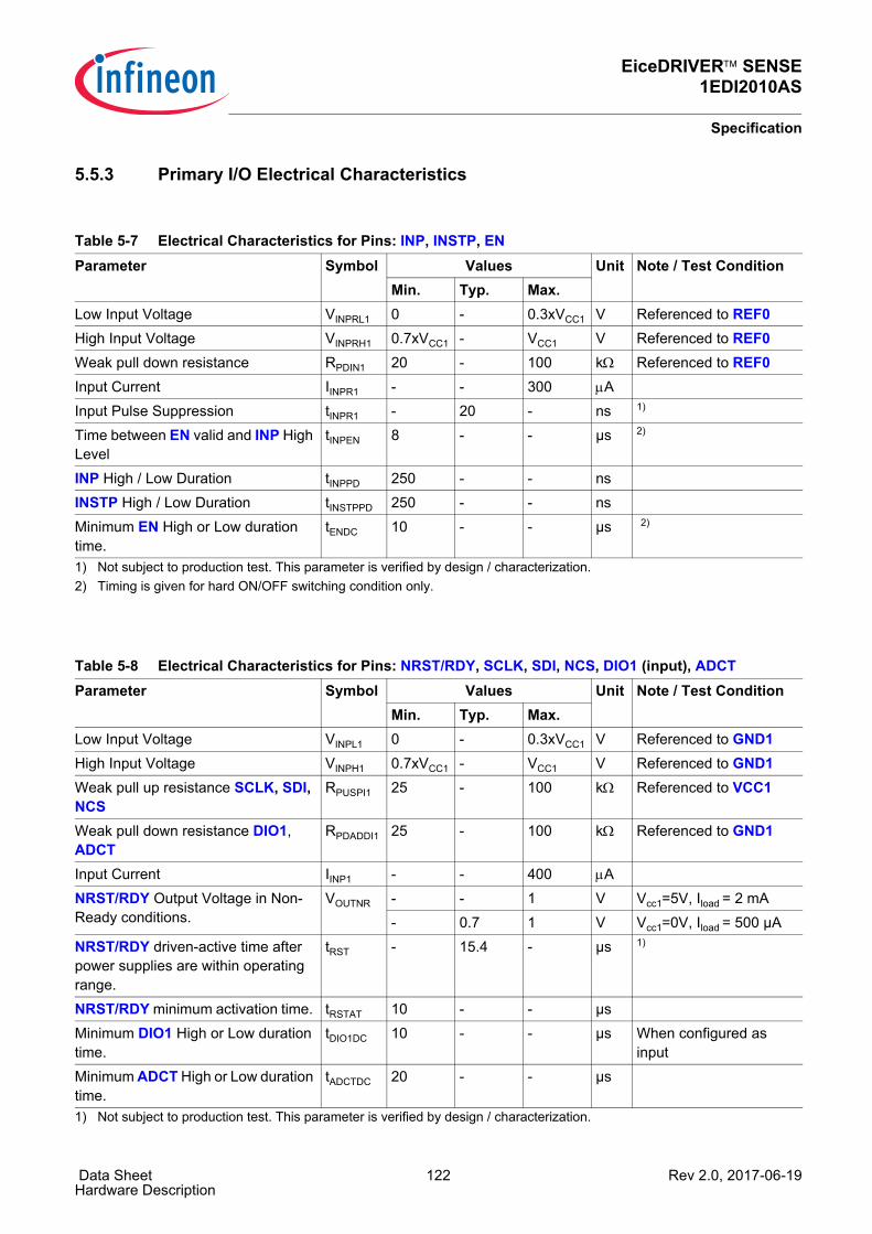
EiceDRIVER™ SENSE1EDI2010AS
Specification
Data Sheet 122 Rev 2.0, 2017-06-19Hardware Description
5.5.3 Primary I/O Electrical Characteristics
Table 5-7 Electrical Characteristics for Pins: INP, INSTP, ENParameter Symbol Values Unit Note / Test Condition
Min. Typ. Max.Low Input Voltage VINPRL1 0 - 0.3xVCC1 V Referenced to REF0High Input Voltage VINPRH1 0.7xVCC1 - VCC1 V Referenced to REF0Weak pull down resistance RPDIN1 20 - 100 kΩ Referenced to REF0Input Current IINPR1 - - 300 μAInput Pulse Suppression tINPR1 - 20 - ns 1)
1) Not subject to production test. This parameter is verified by design / characterization.
Time between EN valid and INP High Level
tINPEN 8 - - µs 2)
INP High / Low Duration tINPPD 250 - - nsINSTP High / Low Duration tINSTPPD 250 - - nsMinimum EN High or Low duration time.
tENDC 10 - - µs 2)
2) Timing is given for hard ON/OFF switching condition only.
Table 5-8 Electrical Characteristics for Pins: NRST/RDY, SCLK, SDI, NCS, DIO1 (input), ADCTParameter Symbol Values Unit Note / Test Condition
Min. Typ. Max.Low Input Voltage VINPL1 0 - 0.3xVCC1 V Referenced to GND1High Input Voltage VINPH1 0.7xVCC1 - VCC1 V Referenced to GND1Weak pull up resistance SCLK, SDI, NCS
RPUSPI1 25 - 100 kΩ Referenced to VCC1
Weak pull down resistance DIO1, ADCT
RPDADDI1 25 - 100 kΩ Referenced to GND1
Input Current IINP1 - - 400 μANRST/RDY Output Voltage in Non-Ready conditions.
VOUTNR - - 1 V Vcc1=5V, Iload = 2 mA- 0.7 1 V Vcc1=0V, Iload = 500 µA
NRST/RDY driven-active time after power supplies are within operating range.
tRST - 15.4 - µs 1)
1) Not subject to production test. This parameter is verified by design / characterization.
NRST/RDY minimum activation time. tRSTAT 10 - - µsMinimum DIO1 High or Low duration time.
tDIO1DC 10 - - µs When configured as input
Minimum ADCT High or Low duration time.
tADCTDC 20 - - µs
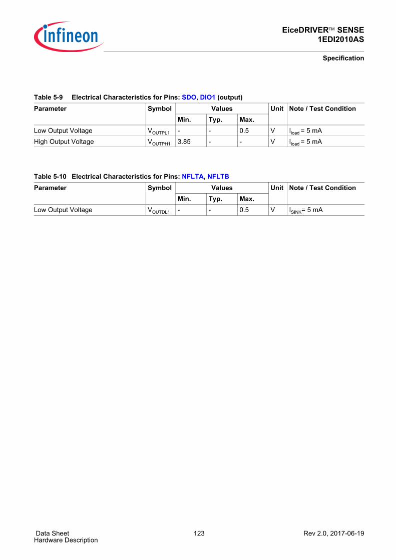
EiceDRIVER™ SENSE1EDI2010AS
Specification
Data Sheet 123 Rev 2.0, 2017-06-19Hardware Description
Table 5-9 Electrical Characteristics for Pins: SDO, DIO1 (output)Parameter Symbol Values Unit Note / Test Condition
Min. Typ. Max.Low Output Voltage VOUTPL1 - - 0.5 V Iload = 5 mAHigh Output Voltage VOUTPH1 3.85 - - V Iload = 5 mA
Table 5-10 Electrical Characteristics for Pins: NFLTA, NFLTBParameter Symbol Values Unit Note / Test Condition
Min. Typ. Max.Low Output Voltage VOUTDL1 - - 0.5 V ISINK= 5 mA

EiceDRIVER™ SENSE1EDI2010AS
Specification
Data Sheet 124 Rev 2.0, 2017-06-19Hardware Description
5.5.4 Secondary I/O Electrical Characteristics
Table 5-11 Electrical Characteristics for Pins: TON, TOFF & GATEParameter Symbol Values Unit Note / Test Condition
Min. Typ. Max.TON & TOFF Output Voltage High V15OH2 VCC2-1 - VCC2+0.3 V Referenced to GND2TON & TOFF Output Voltage Low V15OL2 VEE2-0.3 - VEE2+1 V Referenced to GND2TON & TOFF Source / Sink Current I15O2 1 - - A 1)2)
1) Not subject to production test. This parameter is verified by design / characterization.2) Thermally limited.
GATE Input voltage range V15GATE VEE2 - VCC2 V Referenced to GND2Passive Clamping Voltage VPCLP - - VEE2+1 V Secondary chip not
supplied, TON, TOFF & GATE shorted, ICLAMP= 10 mA.
Passive Clamp Current IPCLP 5 - - mA Secondary chip not supplied, TON, TOFF & GATE shorted,VGATE=VEE2+2V
Table 5-12 Electrical Characteristics for Pins: DEBUG, DIO2(input)Parameter Symbol Values Unit Note / Test Condition
Min. Typ. Max.Low Input Voltage V5INL2 0 - 1.5 V Referenced to GND2High Input Voltage V5INH2 3.5 - 5.5 V Referenced to GND2Weak pull down resistance RPDIN2 20 - 80 kΩ Connected to GND2
Table 5-13 Electrical Characteristics for Pins: DIO2, DACLP (Output)Parameter Symbol Values Unit Note / Test Condition
Min. Typ. Max.Output Voltage High V5OH2 4.0 - 5.25 V Referenced to GND2,
Iload= 2 mA, VREG2= typ.Output Voltage Low V5OL2 0 - 0.5 V Referenced to GND2,
Iload= 2 mA Minimum DIO2 High or Low duration time.
tDIO2DC 10 - - µs When configured as input

EiceDRIVER™ SENSE1EDI2010AS
Specification
Data Sheet 125 Rev 2.0, 2017-06-19Hardware Description
Table 5-14 Electrical Characteristics for Pin: AIPParameter Symbol Values Unit Note / Test Condition
Min. Typ. Max.Voltage Range for Current Source VAIP 0 - 4.5 V IAIPCS= typ. Current Source IAIPCS - 1.05 - mA Rref2 = 23.7 kOhm1)
1) Recommended resistance for specified limits. Other values may lead to malfunction.
Output Current Source Error IAIPCSER -3 - 3 % Deviation from nominal value

EiceDRIVER™ SENSE1EDI2010AS
Specification
Data Sheet 126 Rev 2.0, 2017-06-19Hardware Description
5.5.5 Switching Characteristics
Table 5-15 Switching CharacteristicsParameter Symbol Values Unit Note / Test Condition
Min. Typ. Max.Input to Output Propagation Delay ON
tPDON 175 215 255 ns VCC1=5V, VCC2=15V, VEE2=-8V 1)
Input to Output Propagation Delay OFF
tPDOFF 175 215 255 ns VCC1=5V, VCC2=15V, VEE2=-8V 1)
Input to Output Propagation Delay Distortion (tPDOFF-tPDON)
tPDISTO -50 0 50 ns VCC1=5V, VCC2=15V, VEE2=-8V
Input to Output Propagation Delay Distortion Variation for two consecutive pulses
tPDISTOV - 25 - ns VCC1=5V, VCC2=15V, VEE2=-8V, TJUNC=25°C 2)
Rise Time tRISE - 120 205 ns VCC1=5V, VCC2=15V, VEE2=-8V, CLOAD = 10nF, 10%-90%
- 30 50 ns VCC1=5V, VCC2=15V, VEE2=-8V, no load, 10%-90%
Fall Time tFALL - 150 235 ns VCC1=5V, VCC2=15V, VEE2=-8V, CLOAD = 10nF, 90%-10%
- 60 100 ns VCC1=5V, VCC2=15V, VEE2=-8V, no load, 90%-10%
Voltage during TTOFF Plateau level VGPOF0 5.4 6.0 6.3 V Referenced to GND2, measured at pin TON shorted with TOFF, no VBE compensation, VCC2=15V,TJUNC=25°C
VGPOF1 6.4 7.0 7.3 VVGPOF2 7.3 8.0 8.4 VVGPOF3 8.2 9.0 9.4 VVGPOF4 9.2 10.0 10.5 VVGPOF5 10.1 11.0 11.5 VVGPOF6 11.1 12.0 12.6 VVGPOF7 12.1 13.0 13.6 V
Voltage during TTOFF Plateau level VGPOF0 4.7 5.3 5.6 V Referenced to GND2, measured at pin TON shorted with TOFF, with VBE compensation, VCC2=15V,TJUNC=25°C
VGPOF1 5.7 6.3 6.6 VVGPOF2 6.6 7.3 7.7 VVGPOF3 7.6 8.3 8.7 VVGPOF4 8.5 9.3 9.8 VVGPOF5 9.5 10.3 10.8 VVGPOF6 10.5 11.3 11.9 VVGPOF7 11.5 12.3 12.9 V
EiceDRIVER™ SENSE1EDI2010AS
Specification
Data Sheet 127 Rev 2.0, 2017-06-19Hardware Description
Temperature variation from configured VTTOFF(25°C) @TJ= - 40°C
dVTm40 - -110 - mV 1)3)
Temperature variation from configured VTTOFF(25°C) @TJ= 150°C
dVT150 - 110 - mV 1)3)
TTOFF decrease rate tSLEW - 9 - V/μsTTOFF delay deviation from nominal value
tDEVTTOFF -100 0 100 ns For a target time of 2µs, using the TCF1)2)
TTOFF Plateau Time tTTOFF - 2.6 - μs SRTTOF.RTVAL=26H
Voltage during TTON / WTO Plateau level
VGPON0 5.6 6.0 6.4 V Referenced to GND2, measured at pin TON shorted with TOFF, no VBE compensation, VCC2=15V,TJUNC=25°C
VGPON1 6.5 7.0 7.5 VVGPON2 7.45 8.0 8.5 VVGPON3 8.4 9.0 9.6 VVGPON4 9.35 10.0 10.6 VVGPON5 10.3 11.0 11.7 VVGPON6 11.25 12.0 12.75 V Referenced to GND2,
measured at pin TON shorted with TOFF, no VBE compensation, VCC2=16.5V,TJUNC=25°C
Voltage during TTON / WTO Plateau level
VGPON0 6.2 6.7 7.1 V Referenced to GND2, measured at pin TON shorted with TOFF, with VBE compensation, VCC2=15V,TJUNC=25°C
VGPON1 7.15 7.7 8.15 VVGPON2 8.1 8.7 9.2 VVGPON3 9.0 9.7 10.3 VVGPON4 10.0 10.7 11.2 VVGPON5 10.7 11.4 12 VVGPON6 11.55 12.4 13.1 V Referenced to GND2,
measured at pin TON shorted with TOFF, with VBE compensation, VCC2=16.5V,TJUNC=25°C
TTON Delay tTTON - 8 - μs SCFG.TTONVAL=7FH
DACLP Delay tACL - 5 - μs 4)
1) Values are valid only in case of stand-alone switching transistion.2) Not subject to production test. Parameters are verified by design / characterization.3) Measured without VBE compensation.4) If a following switching sequence is turning off during this time the delay will extend.
Table 5-15 Switching Characteristics (cont’d)
Parameter Symbol Values Unit Note / Test ConditionMin. Typ. Max.
EiceDRIVER™ SENSE1EDI2010AS
Specification
Data Sheet 128 Rev 2.0, 2017-06-19Hardware Description
5.5.6 Desaturation Protection
Table 5-16 DESAT characteristicsParameter Symbol Values Unit Note / Test Condition
Min. Typ. Max.DESAT Input voltage range V15DESAT 0 - VCC2 V Referenced to GND2 DESAT Reference Level VDESAT0 8.5 9 9.5 V VCC2 =15V, VEE2 =-8V
VDESAT1 2.9 3 3.1 VDESAT Pull-up Resistance RDSATPU 19 30 44 kΩ VCC2 =15V, VEE2 =-8V,
VDESAT=2VDESAT Low Voltage VDESATL - 200 - mV Referenced to GND2,
Desat clamping enabled, Isink= 5mA.
DESAT blanking time deviation from programmed value
dtDESATBL -20 - +20 % After transition of the PWM command, assuming a 1 µs programmed blanking time1)
1) Not subject to production test. Parameters are verified by design / characterization.
EiceDRIVER™ SENSE1EDI2010AS
Specification
Data Sheet 129 Rev 2.0, 2017-06-19Hardware Description
5.5.7 Overcurrent Protection
5.5.8 Low Latency Digital Channel
Table 5-17 OCP characteristicsParameter Symbol Values Unit Note / Test Condition
Min. Typ. Max.OC error detection threshold VOCP0 277 300 318 mV Referenced to OCPG
VOCP1 564 600 630 mV Referenced to OCPGOCP blanking time deviation from programmed value
dtOCPBL -20 - +20 % After transition of the PWM command, assuming a 1 µs programmed blanking time1)
1) Not subject to production test. Parameters are verified by design / characterization.OCP Pull-up Resistance RPUOCP2 40 100 175 kΩ to internal 5V reference.
Table 5-18 Digital channel characteristicsParameter Symbol Values Unit Note / Test Condition
Min. Typ. Max.Input to output propagation time primary to secondary
tDPS - 2 4.5 µs 1)
1) Given for single events only. If other communication events occure simultanously max. timing will increase.
Input to output propagation time secondary to primary
tDSP - 2 4.5 µs 1)
EiceDRIVER™ SENSE1EDI2010AS
Specification
Data Sheet 130 Rev 2.0, 2017-06-19Hardware Description
5.5.9 Error Detection Timing
Table 5-19 Error Detection TimingParameter Symbol Values Unit Note / Test Condition
Min. Typ. Max.Dead Time for Shoot Through Protection
tDEAD 800 - 1200 ns Default Value2)
Class A event detection to NFLTA activation
tAFLTA - 2 4.5 μs VCC2=typ., VCC1=typ., VEE2=typ.2)
Class A event detection to turn off sequence activation
tOFFCLA - - 400 ns VTOFF=VCC2 - 1 V, VCC2=typ., VCC1=typ., VEE2=typ.2)
DESAT event detection to turn off sequence activation
tOFFDESAT2 - - 430 ns VTOFF=VCC2 - 1 V, after blanking time elapsed, VCC2=typ., VCC1=typ., VEE2=typ.2)
OCP event occurrence to turn off sequence activation
tOFFOCP2 - - 150 ns VTOFF=VCC2 - 1 V, after blanking time elapsed, VCC2=typ., VCC1=typ., VEE2=typ.2)
Class B event detection to NFLTB activation
tBFLTB - 2 4.5 μs VCC2=typ., VCC1=typ., VEE2=typ.2)
Class B event detection to turn off sequence activation
tOFFCLB2 - - 400 ns VTOFF=VCC2 - 1 V, VCC2=typ., VCC1=typ., VEE2=typ.1)2)
1) Verified by design / characterization. Not tested in production.
Verification Mode time out tVMTO - 15 - ms After a transition from OPM2 to OPM5, SCFG.TOSEN = 0B
1)2)
2) Deviation of the clock needs to be considered.
- 60 - ms After a transition from OPM2 to OPM5, SCFG.TOSEN = 1B
1)2)
Life sign error detection time tLS - 5 - µs After error condition detected by logic.
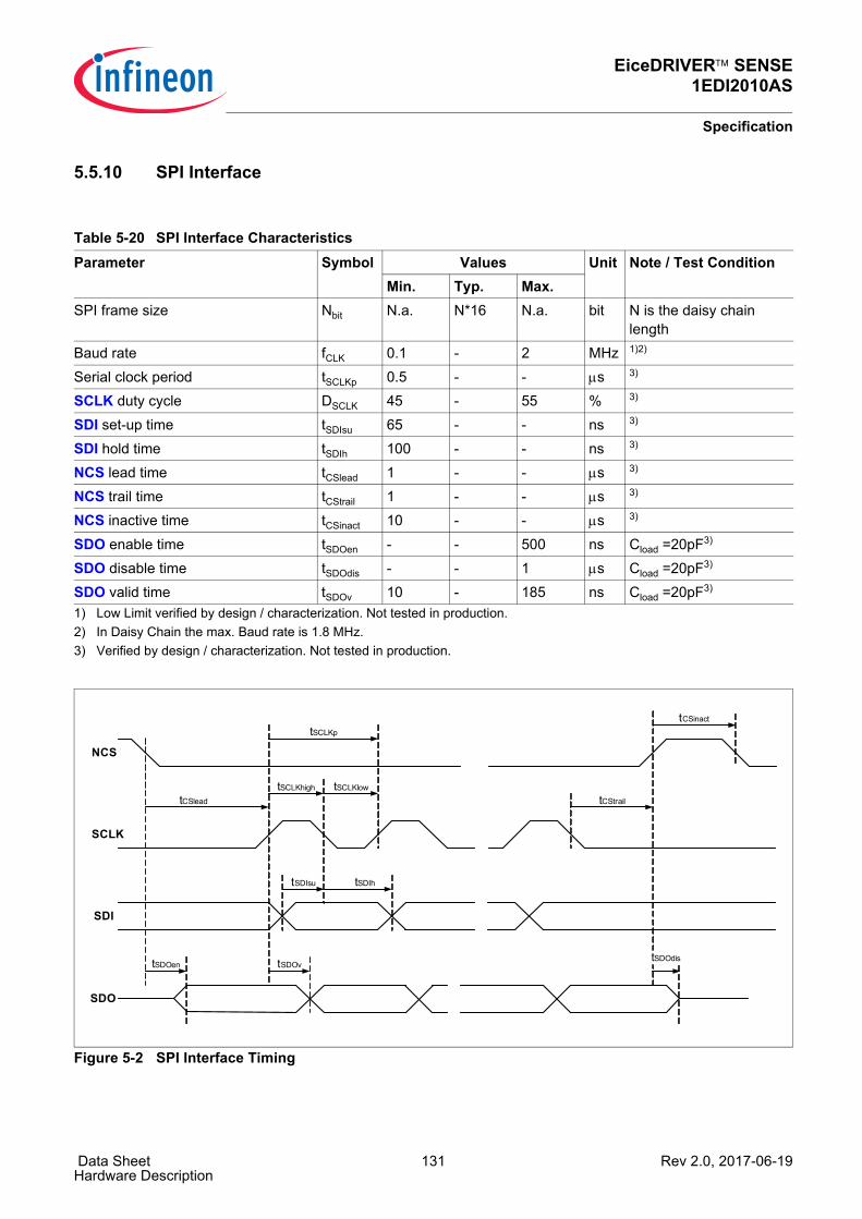
EiceDRIVER™ SENSE1EDI2010AS
Specification
Data Sheet 131 Rev 2.0, 2017-06-19Hardware Description
5.5.10 SPI Interface
Figure 5-2 SPI Interface Timing
Table 5-20 SPI Interface CharacteristicsParameter Symbol Values Unit Note / Test Condition
Min. Typ. Max.SPI frame size Nbit N.a. N*16 N.a. bit N is the daisy chain
lengthBaud rate fCLK 0.1 - 2 MHz 1)2)
1) Low Limit verified by design / characterization. Not tested in production.2) In Daisy Chain the max. Baud rate is 1.8 MHz.
Serial clock period tSCLKp 0.5 - - μs 3)
3) Verified by design / characterization. Not tested in production.
SCLK duty cycle DSCLK 45 - 55 % 3)
SDI set-up time tSDIsu 65 - - ns 3)
SDI hold time tSDIh 100 - - ns 3)
NCS lead time tCSlead 1 - - μs 3)
NCS trail time tCStrail 1 - - μs 3)
NCS inactive time tCSinact 10 - - μs 3) SDO enable time tSDOen - - 500 ns Cload =20pF3)
SDO disable time tSDOdis - - 1 μs Cload =20pF3)
SDO valid time tSDOv 10 - 185 ns Cload =20pF3)
NCS
SCLK
SDO
SDI
tSDOentSDOdis
tCSlead tCStrail
tCSinact
tSCLKhigh tSCLKlow
tSDIsu tSDIh
tSCLKp
tSDOv
EiceDRIVER™ SENSE1EDI2010AS
Specification
Data Sheet 132 Rev 2.0, 2017-06-19Hardware Description
5.5.11 ADC
Table 5-21 ADC parameterParameter Symbol Values Unit Note / Test Condition
Min. Typ. Max.ADC Resolution Res n.a. 8 n.a. bit 1)
1) Verified by design / characterization. Not tested in production.
Sampling time tSMPL - 120 - clock 1), from ADC trigger active to end of sam-pling phase, in OSC2 domain.
Conversion time tCONV - 211 - clock 1), from ADC trigger active to result available in the register, in OSC2 domain.
ADCT trigger signal propagation time tPTRIG - 2 tbd µs 1), from valid signal on pin ADCT to start of conversion, external trigger mode only.
Internal Voltage Range ADC VINT - 2.75 - V Resulting in 93 LSB/VPreamplifier Gain GAIN0,
GAIN1
- 2/3 - - Resulting in 62 LSB/V
GAIN2 - 1 - - Resulting in 93 LSB/VGAIN3 - 2 - - Resulting in 186 LSB/V
ADC Offset VOFF0 - 0.0 - VVOFF1 - 0.5 - VVOFF2 - 1.0 - VVOFF3 - 1.5 - VVOFF4 - 2.0 - V
Offset Error EROFF -3.1 - 3.1 LSB Neg. error results in min. offset.2)
2) Accuracy related parameters are defined when the device is not switching a PWM signal.
Gain Error ERGAIN -5 - 5 Neg. error results in min. gain.2)
INL INL - 1 1.6 LSB 2)
DNL DNL - 0.4 0.75 LSB 2)
Accuracy3)
3) Total Unadjusted Error is the square sum of all worst rms errors (DNL, INL, EROFF and ERGAIN).
TUE - - 6.5 LSB Neg. error results in min. value.2)
Automatic trigger period tATRIG - 4 - ms 1)

EiceDRIVER™ SENSE1EDI2010AS
Specification
Data Sheet 133 Rev 2.0, 2017-06-19Hardware Description
5.5.12 Insulation Characteristics
Table 5-22 Isolation Characteristics referring to IEC 60747-5-2 (VDE 0884 - 10):2006-12Description Symbol Characteristic UnitInstallation classification per EN60664-1, Table 1: rated main voltage less than 150 Vrms rated main voltage less than 300 Vrms rated main voltage less than 600 Vrms
I - IVI - IIII - II
Climatic Classification 40 / 125 / 21Pollution Degree (EN 60664-1) 2Minimum External Clearance CLR 8.12 mmMinimum External Creepage CPG 8.24 mmMinimum Comparative Tracking Index CTI 175Maximum Repetitive Insulation Voltage VIORM 1420 VPEAK
Highest Allowable Overvoltage1)
1) Refer to VDE 0884 for a detailed description of Method a and Method b partial discharge
VIOTM 6000 VPEAK
Maximum Surge Insulation Voltage VIOSM 6000 VPEAK
Table 5-23 Isolation Characteristics referring to UL 1577Description Symbol Characteristic UnitInsulation Test Voltage / 1 min VISO 3750 Vrms
Insulation Test Voltage / 1 sec VISO 4500 Vrms
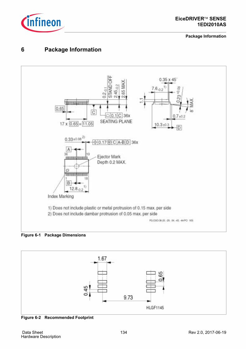
EiceDRIVER™ SENSE1EDI2010AS
Package Information
Data Sheet 134 Rev 2.0, 2017-06-19Hardware Description
6 Package Information
Figure 6-1 Package Dimensions
Figure 6-2 Recommended Footprint