Embed Size (px)
Citation preview

ELE22MIC Lecture 9• MULTIPLEXOR - DATA SELECTOR
• DEMULTIPLEXOR - DATA DISTRIBUTOR
• Parallel to Serial Data Conversion
• External Address Bus Latching
• Address Strobe timing Diagram
• Address Decoding using a 74ls138
• Serial Peripheral Interface - SPI

Multiplexor - Data Selector
• Multiplex (MUX) many inputs to one output
• Switch selects the one signal source from many input signals.
• Like Stereo HiFi source selection switch
Two Input Multiplexor
Output = (Input0 & Select#)
| (Input1 & Select)
Two Input MuxTruth Table
OutputSelectInput 00Input 11

Four Input Multiplexor4 Input MultiplexorTruth TableSelect Line:
Output01Input 000Input 110Input 201Input 311

Eight Input Multiplexor
Eight Input MultiplexorTruth Table
OutputSelect Line:012
Input 0000Input 1100Input 2010Input 3110Input 4001Input 5101Input 6011Input 7111

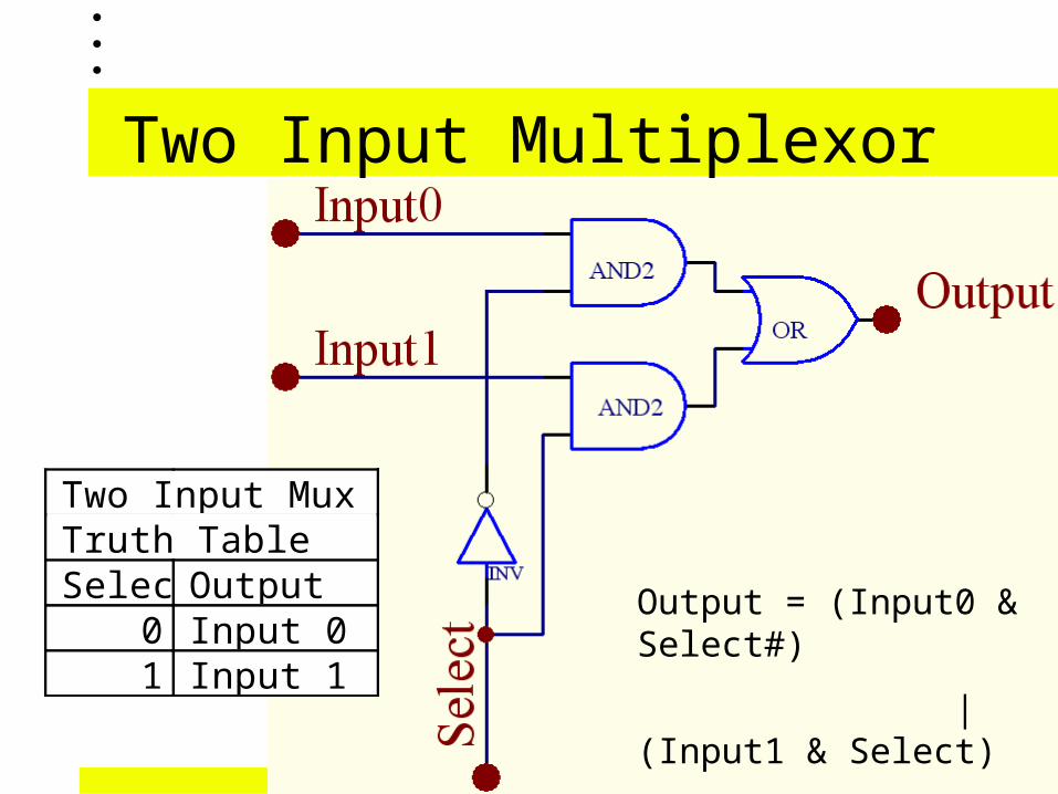
74F151 8-Input MUX
74F151 8-Input MUX
Pin Names and Loading / Fanout
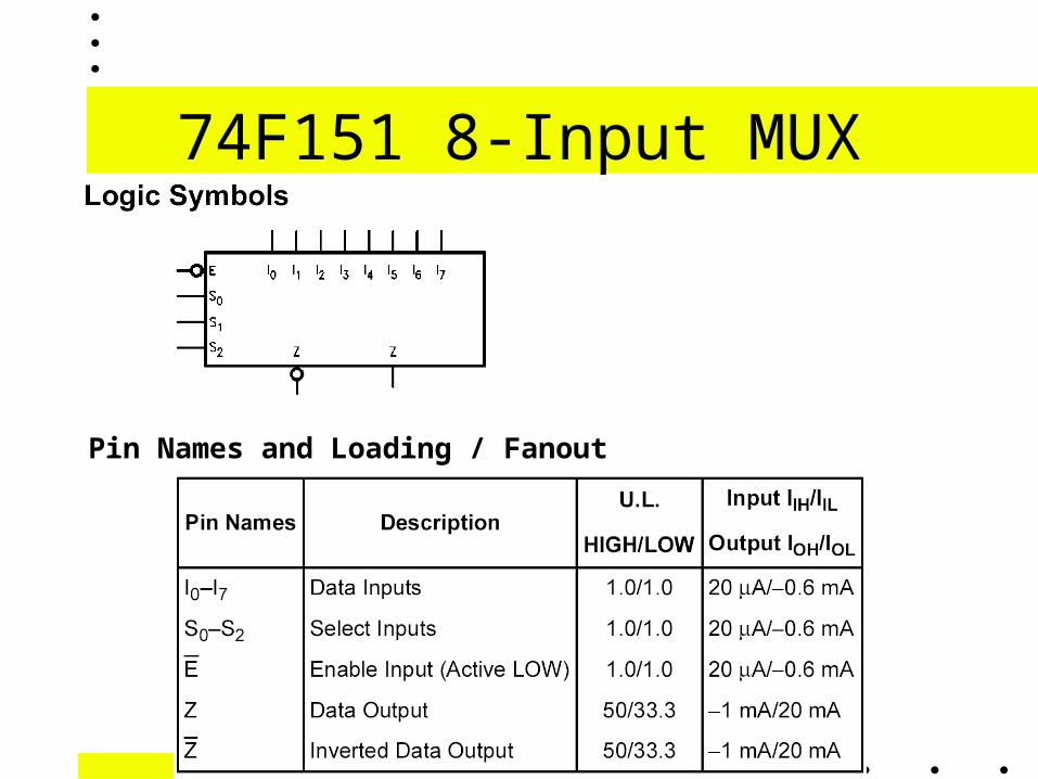
Mux vs DeMux

Parallel I/O

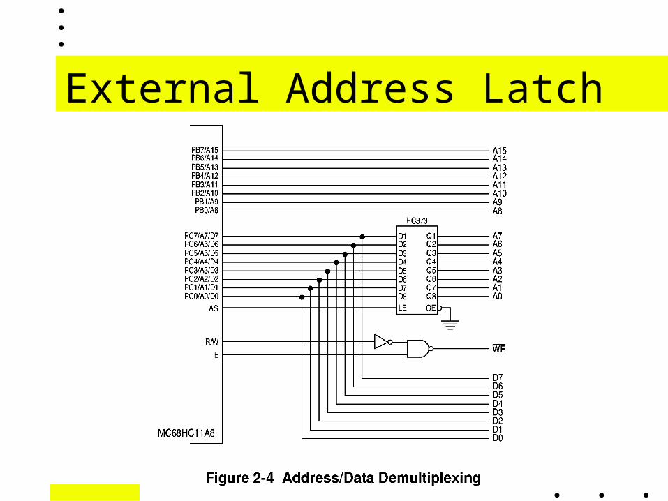
External Address Latch
• The Address Bus (Bits 0..7) and Data Bus (Bits 0..7) are multiplexed onto Port C when in expanded mode - external RAM, ROM & Peripherals
• We want to extend the Address Bus external to the 68HC11 - MAR is presented on C0..PC7/A0..A7/D0..D7 pins
• The 68HC11’s AS pin strobes high to load the address into the external address latch.
• The address latch presents the address onto the system’s external address bus.
External Address Latch

Address Strobe Timing Diagram

Applications of a de-multiplexor
• The Memory Chip Select device used on the original IBM PC is a 74LS138 de-multiplexor.
• The 74LS138 is used to activate 1 of 8 lines based on the conditions of the three binary select inputs A, B & C, and the three enable inputs.
• The 74LS138 Outputs are “Active Low”.
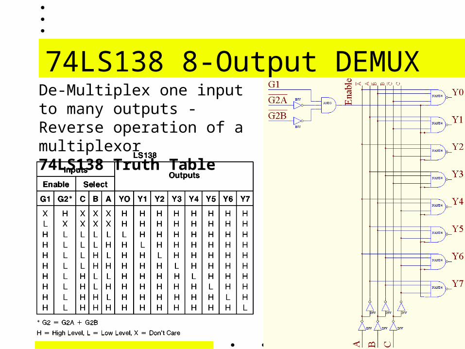
74LS138 8-Output DEMUXDe-Multiplex one input to many outputs -Reverse operation of a multiplexor74LS138 Truth Table

DeMultiplexor• The 74LS138 can be
implemented by the logic shown.
• The 54LS138 is identical in function, but can operate over the “Mil-spec” -55°C to 125°C Temperature Range.
• The 74LS138 can operate over the Commercial 0°C - 70°C Temperature Range.

Memory Select
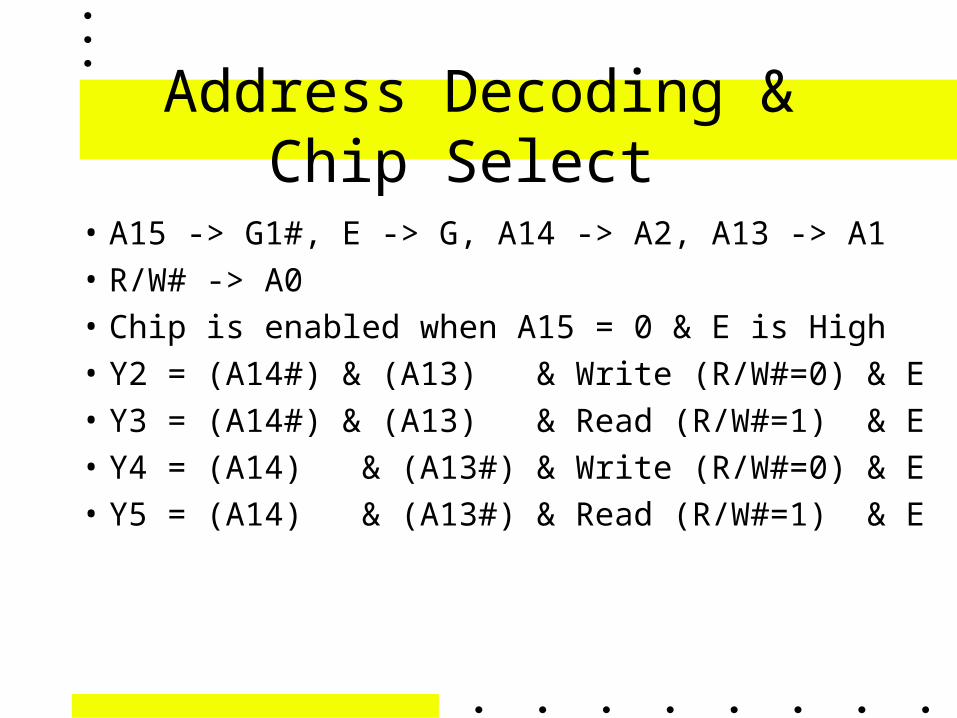
Address Decoding & Chip Select
• A15 -> G1#, E -> G, A14 -> A2, A13 -> A1
• R/W# -> A0
• Chip is enabled when A15 = 0 & E is High
• Y2 = (A14#) & (A13) & Write (R/W#=0) & E
• Y3 = (A14#) & (A13) & Read (R/W#=1) & E
• Y4 = (A14) & (A13#) & Write (R/W#=0) & E
• Y5 = (A14) & (A13#) & Read (R/W#=1) & E
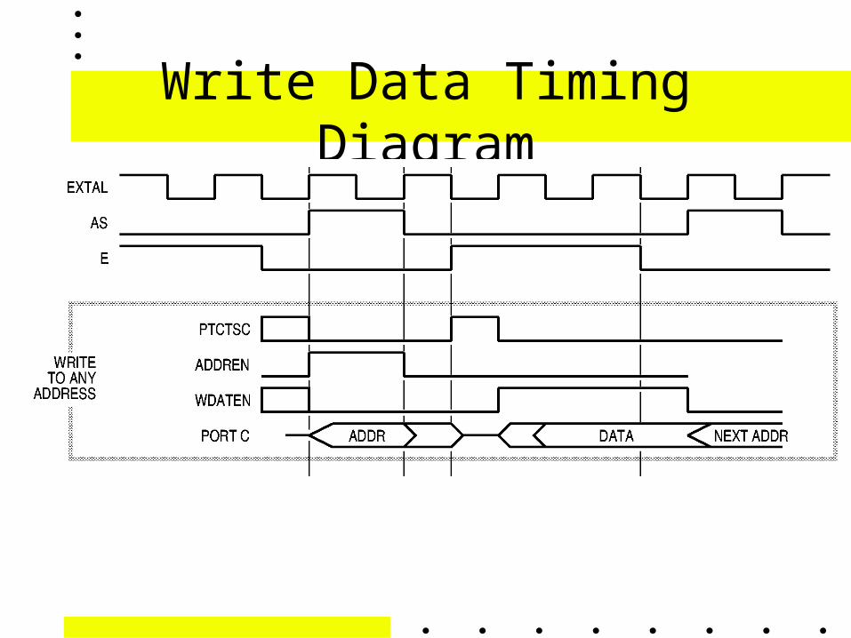
Write Data Timing Diagram
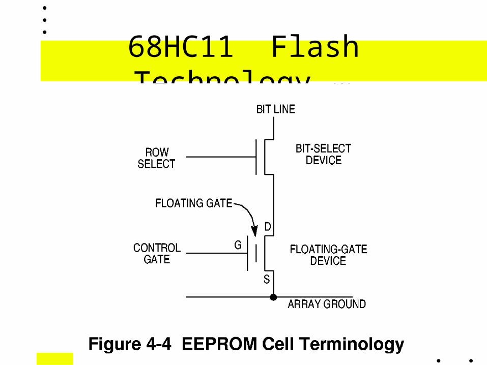
68HC11 Flash Technology (1)
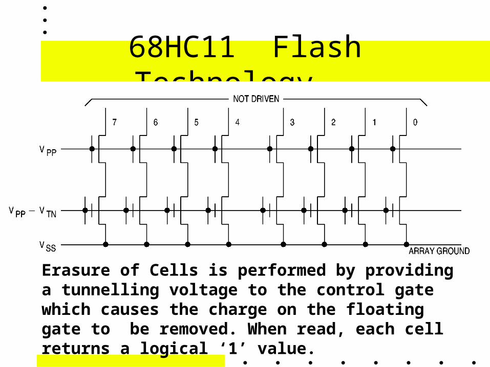
68HC11 Flash Technology (2)
Erasure of Cells is performed by providing a tunnelling voltage to the control gate which causes the charge on the floating gate to be removed. When read, each cell returns a logical ‘1’ value.
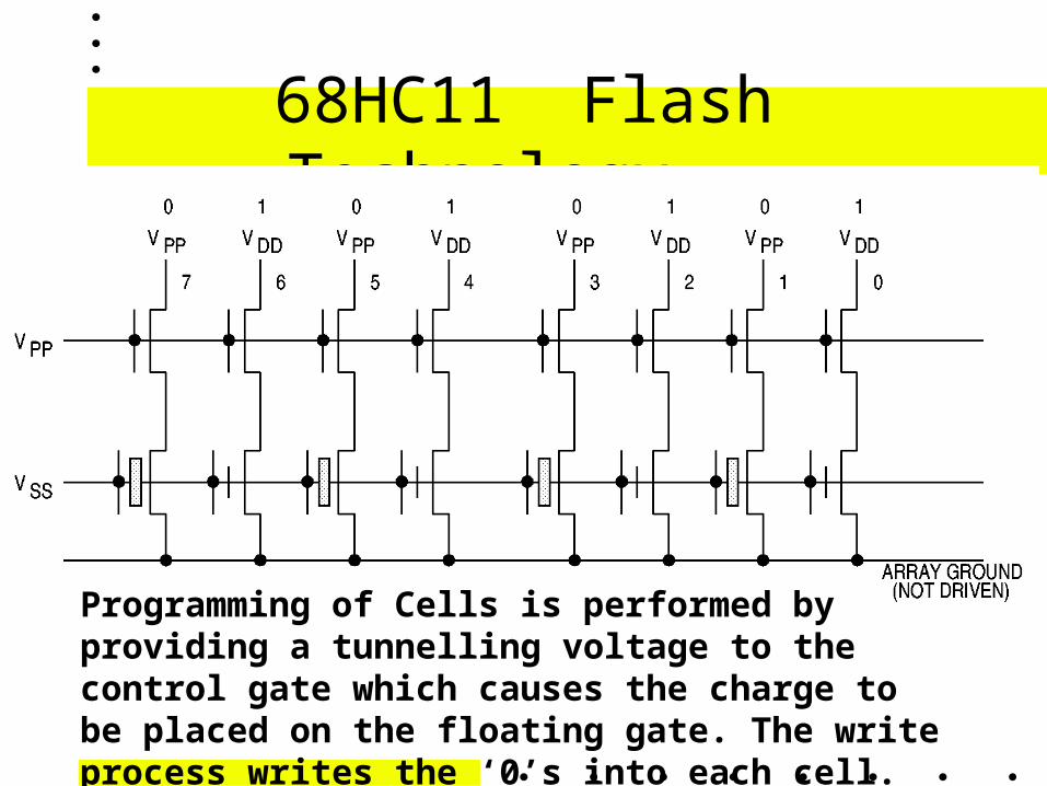
68HC11 Flash Technology (3)
Programming of Cells is performed by providing a tunnelling voltage to the control gate which causes the charge to be placed on the floating gate. The write process writes the ‘0’s into each cell.
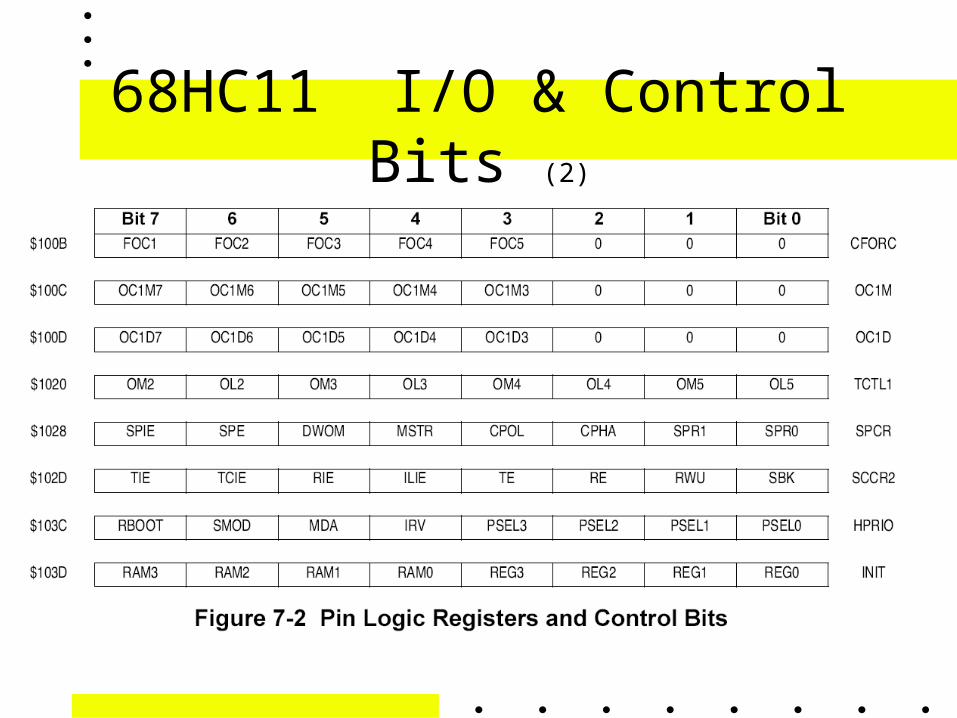
68HC11 I/O & Control Bits (2)

Parallel to Serial Conversion (1)
• Many digital systems use parallel binary data communication for speed (eg CPU data bus, printer etc), but when large distances are to be covered, the number of lines required makes the parallel transmission costly and thus undesirable.
• Referring to the schematic on the next page: A multiplexor can be used convert parallel data to serial data. Parallel data can be latched into the 74F373 gate, then output as a serial data stream from the 74F151 as a binary count sequence is created by the
74LS160.
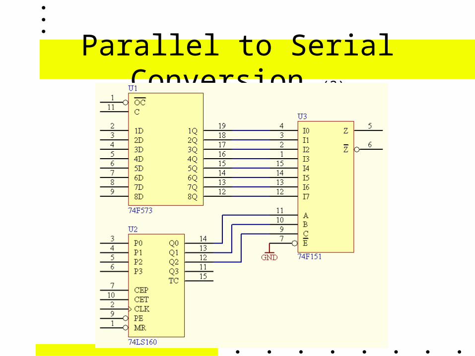
Parallel to Serial Conversion (2)


Logic Family - Propagation Delay (H-L)

Logic Family - Propagation Delay (L-H)

Logic Family - Propagation Delay (3)

Bus Design RulesBus lines have very low line impedances (20 .. 40 Ohms).
• Bus lines have to be terminated to prevent line reflections (signal distortion, circuit malfunctions due to undershoots).
• Take care of propagation times (25 ns/m). Settling time of signals on TTL-type buses is 2 x tp (no incident wave switching).
• Take care of control lines (clock, read, write, etc.).
• Provide shielding between control lines and data / address lines.

Bus Design Rules• A multiplexed data and address bus reduces design problems (50% less signal lines and 50% less line driver).
• Driver output current is 100 mA/line. Provide adequate and low inductance GND return path (simultaneous switching)!
• Rule of thumb: 25% of all backplane connector pins have to be GND lines!
• Use multilayer boards with separate GND and Vcc plane for backplanes.

Acknowledgements• I used Altium Protel 98 and Protel DXP to
create these schematic diagrams
• Logic Timing Diagrams are from Texas Instruments (TI) Logic Selection Guide - Digital Design Seminar
• National Semiconductor data sheets 74LS138.
• Motorola 11rm.pdf Reference Manual