Embed Size (px)
Citation preview
Electrical Characterization of Trough Silicon Via (TSV) depending on Structural and Material Parameters based on 3D Full Wave Simulation
Jun So Pak, Chunghyun Ryu, and Joungho Kim
Terahertz Interconnection and Packaging Laboratory (http://tera.kaist.ac.kr/) Department of Electrical Engineering and Computer Science, Division of Electrical Engineering
Korea Advanced Institute of Science and Technology (KAIST) 373-1 Guseong-dong, Yuseong-gu, Daejeon, 305-701, Korea
Email: [email protected] Phone: +82-42-879-9871, Facsimile: +82-42-869-8058
Abstract
In this paper, we show the electrical characteristics of TSV (Through Silicon Via) depending on structural parameters such as TSV pitch, TSV height, TSV size and thickness of SiO2 for DC leakage blocking between TSV and silicon substrate, and material parameter of silicon substrate such as silicon resistivity in case of single silicon substrate. And we also show X-talk characteristics of two TSVs depending on distance of two signal TSVs and different locations of two signal TSVs and two ground TSVs in array type arrangement of TSV. Additionally, we show the electrical characteristics of TSV depending on number of stacked TSVs. All electrical characterizations on this paper are obtained using commercial 3-D full wave simulator and spice type circuit simulator such as HFSS of Ansoft Corporation and ADS of Agilent Corporation, respectively.
1. Introduction System in Package (SiP) is the highest technology to make
mobile electronic devices such as cell phones, personal digital assistants (PDAs), digital cameras, and etc, be small enough for men to carry them in one hand. Therefore, the demand for SiP is dramatically increasing and predicted from 1,573 million units in 2007 to 2,495 million units in 2011 (Fig. 1), and the most part of SiP applications in 2007 is concentrated in cell phone by 71 %. [1]
Figure 1. System in Package (SiP) annual growth. However, the conventional SiP is manufactured on two-
dimensional (2-D) package substrate. For example, a few chips are located on a single package substrate, and they are interconnected by long wire-bonding. Consequently, though
their individual data processing speed is high, the overall system performance and the package size are not enough to meet current demands due to long interconnections.
Figure 2. 3-D stacked chip package annual growth.
Therefore, three-dimensionally (3-D) stacked chip
packages are highly needed to get short signal and power supply paths using short interconnections between semiconductor chips and to raise number of chip in a single small size package. These packages are suitable for small and lightweight high performance mobile electronic devices. Also, these devices need low power consumption package for long usage of a storage battery in one time charging.
At the first trying for 3-D stacked chip packages, a wire-bonding interconnection is adopted by Hynix, Samsung, and Akita Elpida. They stacked very thin chips (25 µm ~ 30 µm thickness/chip) in shape of stairs and connected the chips each other and the chips to printed circuit board (PCB). This method efficiently reduces wire-bonding length between chips and SiP size. Moreover, it increases chip density in a unit area. The high chip density is very important in case of memory chip stacking because high end mobile electronic devices is getting more and more volume of memory size. The world wide market volume of 3-D stacked chip package is predicted from 2,065 million units in 2007 to 5,227 million units in 2011, which is almost double. [1] (Fig. 2)
As the packages are including high-speed integrated circuits (ICs), conventional bonding-wire interconnections for the 3-D stacked chip packages are not the best way to guarantee good signal integrity (SI) and low power consumption due to their large equivalent series inductance (ESL) and large conduction loss. Therefore, the short length interconnection technologies are developing. One of them is
Authorized licensed use limited to: Korea Advanced Institute of Science and Technology. Downloaded on February 24,2010 at 20:52:49 EST from IEEE Xplore. Restrictions apply.

flip chip technology, which is difficult to meet the demands of high chip density with small thickness package due to its relatively large size ball and pitch. The other state-of-the-art technology is a through silicon via (TSV), which routes the electrical signal and power supply pathes through all chips in the stack, rather than wire-bonding around lower chip to the substrate below. TSV of a vertical interconnection structure is a promising interconnection method to connect vertically stacked chips with the shortest interconnection, which means the lowest inductance and conduction loss interconnection are provided to both signal and power supply paths between semiconductor chips. Therefore, in order to design advanced 3-D stacked chip package using TSV, the precisely evaluated electrical characteristics of TSV including SI of single TSV, crosstalk (X-talk) of two adjacent TSVs, and power integrity (PI) depending on TSV structure and TSV silicon substrate material are needed. However, since most parts of TSV manufacturing technology are under developing, it is very difficult to evaluate the electrical characteristics of TSV through measurements according to various structures and silicon substrate materials. Consequently, 3D full wave simulation is adequate to extract the electrical characteristics of TSV, and spice type simulation is so to predict the electrical characteristics of 3-D stacked TSVs.
2. 3-D Full Wave & Spice Type Circuit Simulations First of all, in order to evaluate electrical characteristics of
TSV depending on structural parameters such as TSV pitch, TSV height, TSV size and thickness of SiO2 for DC leakage blocking between TSV and silicon substrate, and material parameter of silicon substrate such as silicon resistivity in case of single silicon substrate, we have determined the structural parameters and the material parameter of the standard TSV structure according to [2]-[4] and advices of the authors of [3].
Figure 3. Structure of Standard TSV for 3-D full wave simulation.
The standard TSV has two-TSV type, one is for the signal
path and the other is for the signal return current path. Since two return current path interconnections are not popular in practical case, we have selected two-TSV type, which is different from three-TSV type, one is for the signal path and the rest two at both sides are for the signal return current
paths. The signal return current path is usually known as Ground or GND.
Figure 4. Structure of top and side surfaces of standard TSV
(the white circle part of Fig. 3). And it has 200 µm TSV pitch (distance between the
centers of two TSVs), 82 µm TSV height (embedded part of TSV in silicon substrate is 80 µm), 80 µm TSV size (top view shape of TSV is square and aspect ratio of TSV is 1) and 0.2 µm thickness of SiO2 between TSV and silicon substrate. And silicon substrate has 10 Ω⋅cm (resistivity), which is same of 10 S/m (conductivity), and its one edge and thickness are 1 mm and 80 µm respectively. (Figs. 3 and 4)
(a) (b)
Figure 5. Evaluated S21 magnitude (a) and phase (b) of standard TSV using 3-D full wave simulation.
The standard TSV (figs. 3 and 4) was simulated using 3-D
full wave simulator and its electrical characteristics were evaluated as shown in Fig. 5. Usually, an interconnection line is characterized using S-parameters. In two-port system with signal input and output ports, S-parameters are defined by S11, S12, S21, and S22. Under passive only system, S11 and S22 are same, and S12 and S21 are also same. And S21 is a
1E9 1E101E8 3E10
-0.75
-0.50
-0.25
-1.00
0.00
Frequency [Hz]
S21
mag
nitu
de [d
B]
1E9 1E101E8 3E10
-10
-5
-15
0
Frequency [Hz]
S21
pha
se [D
egre
e]
Authorized licensed use limited to: Korea Advanced Institute of Science and Technology. Downloaded on February 24,2010 at 20:52:49 EST from IEEE Xplore. Restrictions apply.
typical electrical characteristic of an interconnection, and we show only S21 values for electrical characteristics of standard TSV. Fig. 5 show very similar line shapes as shown in [2], where three-TSV type used and its structure is a little different. But there are discrepancies between our results and those of [2]-[3] because our two-TSV type has larger DC resistance and capacitance due to number of TSVs and square shape of TSV. As number of return current paths is larger, DC resistance and capacitance is smaller. As faced area is wider (square case is wider than circle one), capacitance is larger.
Then, the transmitted data stream through the standard TSV was simulated with the evaluated S-parameters from 3-D full wave simulation. The transmitted data stream was evaluated by Eye-diagram in case of 107-1 pseudo random bit sequence (PRBS) using spice type circuit simulator. The source for the simulation has 1 Vp-p and 50 Ω source termination. The standard TSV is terminated by shunt connected 50 Ω and 1 pF. We have obtained the Eye-diagrams of 1 Gbps (bit per second), 2 Gbps, 5 Gbps, and 10 Gbps PRBSs. All PRBSs was assumed that they have 10 % rising and falling times of single bit duration. For example, 1 Gbps has 1 ns (nano second) bit duration and it has 0.1 ns rising and falling times. In this paper, two Eye-diagrams of 2 Gbps and 10 Gbps are shown in Fig. 6.
Figure 6. The simulated Eye-diagrams of 2 Gbps (a) and 10
Gbps (b) PRBSs after passing through the standard TSV. As shown in Fig. 6, the large resistance and capacitance of
the standard TSV reduce eye open area and increase rising and falling times. In both cases of 2 Gbps and 10 Gbps, the eye open areas are reduced by 0.05 V and 0.2 V comparing
with source waveforms of 0.5 Vp-p respectively. And the rising and falling times are increased from 0.05 ns and 0.01 ns to 0.2 ns (4 times) and 0.1 ns (10 times) respectively. Therefore, in order to use TSV in high speed system over 10 Gbps, the large capacitance problem of TSV must be solved by increasing SiO2 thickness between TSV and silicon substrate, which means reducing capacitance of TSV. And reducing TSV height is very helpful to keep eye open area wide by adopting thinner TSV structure.
The practical application of TSV is 3-D stacked chip package. Therefore, the electrical characteristics of 3-D stacked TSVs are also very import and must be evaluated. We evaluated them using the evaluated S-parameters in simulation level. In our approach, we did not consider any other interconnection and bonding structures such as TSV bump pads and bump itself. We have simulated the 2 stacked standard TSVs (Fig. 7), the 5 stacked standard TSVs (Fig. 8), and the 10 stacked TSVs (Fig. 9) under applying 2 Gbps ((a)s of Figs. 7, 8, and 10) and 10 Gbps ((b)s of Figs. 7, 8, and 10) PRBSs to them.
(a) 2 Gbps PRBS (b) 10 Gbps PRBS Figure 7. 2 stacked standard TSVs.
(a) 2 Gbps PRBS (b) 10 Gbps PRBS Figure 8. 5 stacked standard TSVs.
(a) 2 Gbps PRBS (b) 10 Gbps PRBS Figure 9. 10 stacked standard TSVs.
Through three (a) figures of Figs. 7, 8, and 9, the 2 Gbps
PRBS is affected by total resistance of 3-D stacked TSVs and only eye open area is reduced according to increasing number of TSVs. If a specification of vertical eye open is 60 % comparing to original waveform, in this case a specification is 0.3 Vp-p, 10 stacked standard TSVs cannot be used in any PRBS data rates due to its large resistance. And three (b) figures of Figs. 7, 8, and 9, the 10 Gbps PRBS is affected by both total resistance and capacitance of 3-D stacked TSVs. Then, eye open area is reduced in both vertical (resistance)
Authorized licensed use limited to: Korea Advanced Institute of Science and Technology. Downloaded on February 24,2010 at 20:52:49 EST from IEEE Xplore. Restrictions apply.
1E9 1E101E8 3E10
-6
-5
-4
-3
-2
-1
-7
0
Frequency [Hz]
S2
1 m
ag
nitu
de
[dB
]
1E9 1E101E8 3E10
-5
-3
-1
-7
0
Frequency [Hz]
S2
1 m
ag
nitu
de
[dB
]
0 20 40 60 80 100 120 140 160 180 200-20 220
0.0
0.1
0.2
0.3
0.4
-0.1
0.5
Time [ps]
Eye
_10G
bps_
5TS
V
1E9 1E101E8 3E10
-5
-3
-1
-7
0
Frequency [Hz]
S2
1 m
ag
nitu
de
[dB
]
0 20 40 60 80 100 120 140 160 180 200-20 220
-0.0
0.1
0.2
0.3
0.4
-0.1
0.5
Time [ps]
Eye
_10G
bps_
5TS
V
1E9 1E101E8 3E10
-5
-3
-1
-7
0
Frequency [Hz]
S2
1 m
ag
nitu
de
[dB
]
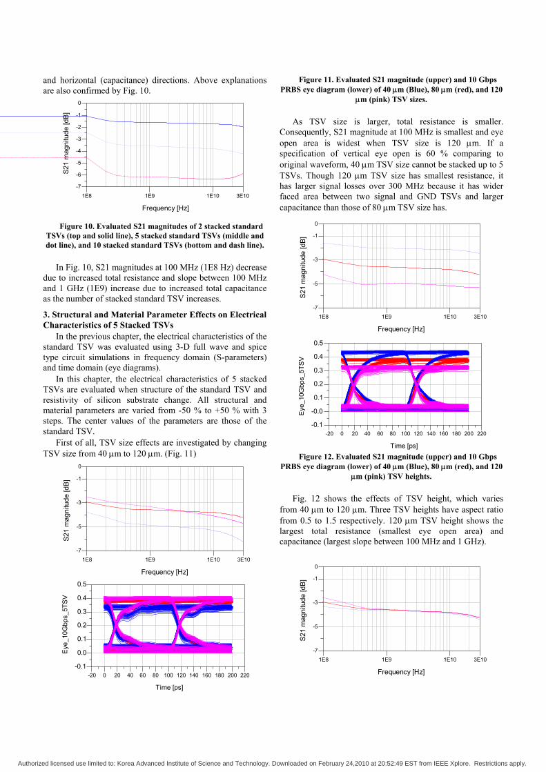
and horizontal (capacitance) directions. Above explanations are also confirmed by Fig. 10.
Figure 10. Evaluated S21 magnitudes of 2 stacked standard
TSVs (top and solid line), 5 stacked standard TSVs (middle and dot line), and 10 stacked standard TSVs (bottom and dash line).
In Fig. 10, S21 magnitudes at 100 MHz (1E8 Hz) decrease
due to increased total resistance and slope between 100 MHz and 1 GHz (1E9) increase due to increased total capacitance as the number of stacked standard TSV increases.
3. Structural and Material Parameter Effects on Electrical Characteristics of 5 Stacked TSVs
In the previous chapter, the electrical characteristics of the standard TSV was evaluated using 3-D full wave and spice type circuit simulations in frequency domain (S-parameters) and time domain (eye diagrams).
In this chapter, the electrical characteristics of 5 stacked TSVs are evaluated when structure of the standard TSV and resistivity of silicon substrate change. All structural and material parameters are varied from -50 % to +50 % with 3 steps. The center values of the parameters are those of the standard TSV.
First of all, TSV size effects are investigated by changing TSV size from 40 µm to 120 µm. (Fig. 11)
Figure 11. Evaluated S21 magnitude (upper) and 10 Gbps PRBS eye diagram (lower) of 40 µm (Blue), 80 µm (red), and 120
µm (pink) TSV sizes. As TSV size is larger, total resistance is smaller.
Consequently, S21 magnitude at 100 MHz is smallest and eye open area is widest when TSV size is 120 µm. If a specification of vertical eye open is 60 % comparing to original waveform, 40 µm TSV size cannot be stacked up to 5 TSVs. Though 120 µm TSV size has smallest resistance, it has larger signal losses over 300 MHz because it has wider faced area between two signal and GND TSVs and larger capacitance than those of 80 µm TSV size has.
Figure 12. Evaluated S21 magnitude (upper) and 10 Gbps PRBS eye diagram (lower) of 40 µm (Blue), 80 µm (red), and 120
µm (pink) TSV heights. Fig. 12 shows the effects of TSV height, which varies
from 40 µm to 120 µm. Three TSV heights have aspect ratio from 0.5 to 1.5 respectively. 120 µm TSV height shows the largest total resistance (smallest eye open area) and capacitance (largest slope between 100 MHz and 1 GHz).
Authorized licensed use limited to: Korea Advanced Institute of Science and Technology. Downloaded on February 24,2010 at 20:52:49 EST from IEEE Xplore. Restrictions apply.

0 20 40 60 80 100 120 140 160 180 200-20 220
-0.0
0.1
0.2
0.3
0.4
-0.1
0.5
Time [ps]
Eye
_10G
bps_
5TS
V
1E9 1E101E8 3E10
-5
-3
-1
-7
0
Frequency [Hz]
S2
1 m
ag
nitu
de
[dB
]
0 20 40 60 80 100 120 140 160 180 200-20 220
0.0
0.1
0.2
0.3
0.4
-0.1
0.5
Time [ps]
Eye
_10G
bps_
5TS
V
1E9 1E101E8 3E10
-5
-3
-1
-7
0
Frequency [Hz]
S2
1 m
ag
nitu
de
[dB
]0 20 40 60 80 100 120 140 160 180 200-20 220
-0.0
0.1
0.2
0.3
0.4
-0.1
0.5
Time [ps]E
ye_1
0Gbp
s_5T
SV
Figure 13. Evaluated S21 magnitude (upper) and 10 Gbps PRBS eye diagram (lower) of 0.1 µm (Blue), 0.2 µm (red), and
0.3 µm (pink) 0.2 µm thickness of SiO2 between TSV and silicon substrate.
As shown in Fig. 13, the SiO2 thickness between TSV and
silicon substrate affects below 1 GHz frequency range and rising and falling times. Primarily, 0.3 µm SiO2 thickness shows still too large capacitance to apply to over 10 Gbps PRBS system as shown S21 magnitudes at 100 MHz of Fig. 13.
Figure 14. Evaluated S21 magnitude (upper) and 10 Gbps PRBS eye diagram (lower) of 100 µm (Blue), 200 µm (red), and
300 µm (pink) TSV pitchs. As TSV pitch reduces, S21 magnitude of high frequency
range reduces. Consequently, this bad high frequency electrical characteristic makes eye open area reduce critically.
Figure 15. Evaluated S21 magnitude (upper) and 10 Gbps PRBS eye diagram (lower) when the resistivities of silicon
substrate embedding TSV vary from 5 Ω⋅cm (Blue), 10 Ω⋅cm (red), and 15 Ω⋅cm (pink).
As the resistivity of silicon substrate increases, it is hard
for the DC and high frequency leakage currents to directly flow from signal TSV to GND TSV. Therefore, 15 Ω⋅cm silicon substrate TSV shows the largest S21 magnitude over all frequency range, the widest eye open area and the smallest rising and falling times as shown in Fig. 15. Consequently, for the higher frequency applications, a higher resistivity silicon substrate embedding TSV must be selected.
4. Crosstalk (X-talk) between Two Pairs Signal & GND TSVs
The beginning of TSV development is to acquire high chip density. Therefore, the density of TSV is also high. In this environment, a crosstalk problem appears between two adjacent singal TSVs. In this chapter, we evaluate crosstalks depending on the distance of two signal TSVs and the location of two signal TSVs and two GND TSVs. (Fig. 16)
Figure 16. Location of two pairs of the standard TSVs for Crosstalk evaluations.
Authorized licensed use limited to: Korea Advanced Institute of Science and Technology. Downloaded on February 24,2010 at 20:52:49 EST from IEEE Xplore. Restrictions apply.

1E9 1E101E8 3E10
-80
-70
-60
-50
-40
-90
-30
Frequency [Hz]
Cro
ssta
lk M
agni
tude
[dB
]
1E9 1E101E8 3E10
-80
-70
-60
-50
-40
-90
-30
Frequency [Hz]
Cro
ssta
lk M
agni
tude
[dB
]
1E9 1E101E8 3E10
-80
-70
-60
-50
-40
-90
-30
Frequency [Hz]
Cro
ssta
lk M
agni
tude
[dB
]
We simulated 6 cases with 2 pairs of the standard TSV and divided them into two groups, one is SGSG (left side of Fig. 16) and the other is SGGS (right side of Fig. 16). Each group is named according to the order of TSV’s role. And each group was simulated in three cases according to the distance between two pairs of signal and GND TSVs such as 200 µm, 300 µm, and 400 µm.
First, three SGSG TSV locations was evaluated and compared as shown in Fig. 17 (a). As easily expected, the distance between two signal TSVs is larger, the cross talk level is going down. In case of SGGS TSV location, the same tendency is found from Fig. 17 (b).
(a) (b) Figure 17. Comparison of three SGSG TSV locations (a) and
three SGGS TSV locations (b). 200 µm, 300 µm, and 400 µm distances between two signal TSVs are top, middle, and bottom
lines respectively. Figure 18. Comparison of two 200 µm distance cases. Upper
and lower lines are the crosstalk magnitudes of SGSG and SGGS TSV locations respectively.
One more interesting thing in Fig. 17 is that the crosstalk
magnitudes of SGSG TSV locations are larger than those of SGGS TSV locations comparing two same distance cases.
The crosstalk magnitudes of two 200 µm distance cases are compared in Fig. 18. The difference of two cases is from 10 dB to 20 dB. This is very important point for TSV designer to keep in mind because just change of TSV role can reduce crosstalk magnitude. Especially in high frequency applications of TSV, crosstalk problem is very critical to obtain the maximum system performance.
Conclusions In this paper, we show the electrical characteristics of
TSV (Through Silicon Via) depending on structural and material parameters in case of single silicon substrate. And we also show X-talk characteristics of two TSVs depending on distance of two signal TSVs and different locations of two signal TSVs and two ground TSVs. Additionally, we show the electrical characteristics of TSV depending on number of stacked TSVs. All electrical characterizations on this paper are obtained using commercial 3-D full wave simulator and spice type circuit simulator such as HFSS of Ansoft Corporation and ADS of Agilent Corporation, respectively.
The important points for high frequency applications of 3-D stacked TSV are reducing total resistance, enlarged TSV size and reduced TSV height, reducing total capacitance, enlarged TSV pitch and increased SiO2 thickness over micrometer, and using high resistivity silicon substrate. And in order to design low crosstalk TSV, the cross locations of signal and GND TSVs are very effective method.
Acknowledgments This work was supported by the IT R&D program of
MIC/IITA. [2005-S-118-02, Development of High-Performance and Smallest SiP Technology]
References 1. Sandra Winkler, Advanced IC Packaging, 2007 Edition,
Electronic Trend Publications (2007) 2. D. M. Jang, C. Ryu, K. Y. Lee, B. H. Cho, J. Kim, T. S.
Oh, W. J. Lee, and J. Yu, “Development and evaluation of 3-D SiP with vertically interconnected through silicon vias (TSV),” Proc 2007 Elect. Comp. and Tech. Conf, Reno, Nevada, May. 2007, pp. 847-852.
3. C. Ryu, J. Lee, H. Lee, K. Lee, T. Oh, J. Kim, " High Frequency Electrical Model of Through Wafer Via for 3-D Stacked Chip Packaging", Electronics System-integration Technology Conf, vol 1, pp. 215-220, Sept. 2006.
4. C. Ryu, D. Chung, Junho Lee, K. Lee, T. Oh, J. Kim, "High frequency electrical circuit model of chip-to-chip vertical via interconnection for 3-D chip stacking package", IEEE 14th Topical Meeting on Electrical Performance of Electronic Packaging, pp. 151-154, Oct. 2005.
Authorized licensed use limited to: Korea Advanced Institute of Science and Technology. Downloaded on February 24,2010 at 20:52:49 EST from IEEE Xplore. Restrictions apply.


![ECTC 2008 리뷰 전자부품및패키징컨퍼런스 2008 리뷰_ 전자... · 2012-06-14 · 다. TSV(through silicon via)[1], WLP(wafer level packaging) 등과같은실리콘기반으로의패키징기술들도](https://img.pdfslide.net/doc/110x75/5ee125a9ad6a402d666c21c0/ectc-2008-ee-eeoee-2008-ee-2012-06-14.jpg)