Embed Size (px)
Citation preview
Electrolyte-gated transistors for neuromorphic applicationsHeyi Huang, Chen Ge, Zhuohui Liu, Hai Zhong, Erjia Guo, Meng He, Can Wang, Guozhen Yang, and Kuijuan Jin
Citation: H Y Huang, C Ge, Z H Liu, H Zhong, E J Guo, M He, C Wang, G Z Yang, and K J Jin, Electrolyte-gated transistors forneuromorphic applications[J]. J. Semicond., 2021, 42(1).
View online: https://doi.org/10.1088/1674-4926/42/1/013103
Articles you may be interested in
Charge transport and quantum confinement in MoS2 dual-gated transistors
Journal of Semiconductors. 2020, 41(7), 072904 https://doi.org/10.1088/1674-4926/41/7/072904
Study on the short-term synaptic plasticity in Ion-Gel gated graphene electric-double-layer synaptic transistors
Journal of Semiconductors. 2020, In press.
Neuromorphic vision sensors: Principle, progress and perspectives
Journal of Semiconductors. 2020, In press.
Towards engineering in memristors for emerging memory and neuromorphic computing: A review
Journal of Semiconductors. 2020, In press.
Resistive switching characteristic of electrolyte-oxide-semiconductor structures
Journal of Semiconductors. 2017, 38(8), 084003 https://doi.org/10.1088/1674-4926/38/8/084003
Artificial neuron synapse transistor based on silicon nanomembrane on plastic substrate
Journal of Semiconductors. 2017, 38(6), 064006 https://doi.org/10.1088/1674-4926/38/6/064006
Follow JOS WeChat public account for more information
Electrolyte-gated transistors for neuromorphic applications
Heyi Huang1, 2, Chen Ge1, 2, †, Zhuohui Liu1, 2, Hai Zhong1, Erjia Guo1, 2, Meng He1, Can Wang1, 2, 3,Guozhen Yang1, and Kuijuan Jin1, 2, 3, †
1Beijing National Laboratory for Condensed Matter Physics, Institute of Physics, Chinese Academy of Sciences, Beijing 100190, China2School of Physical Sciences, University of Chinese Academy of Science, Beijing 100049, China3Songshan Lake Materials Laboratory, Dongguan 523808, China
Abstract: Von Neumann computers are currently failing to follow Moore’s law and are limited by the von Neumann bottleneck.To enhance computing performance, neuromorphic computing systems that can simulate the function of the human brain arebeing developed. Artificial synapses are essential electronic devices for neuromorphic architectures, which have the ability toperform signal processing and storage between neighboring artificial neurons. In recent years, electrolyte-gated transistors(EGTs) have been seen as promising devices in imitating synaptic dynamic plasticity and neuromorphic applications. Amongthe various electronic devices, EGT-based artificial synapses offer the benefits of good stability, ultra-high linearity and re-peated cyclic symmetry, and can be constructed from a variety of materials. They also spatially separate “read” and “write” opera-tions. In this article, we provide a review of the recent progress and major trends in the field of electrolyte-gated transistors forneuromorphic applications. We introduce the operation mechanisms of electric-double-layer and the structure of EGT-based arti-ficial synapses. Then, we review different types of channels and electrolyte materials for EGT-based artificial synapses. Finally,we review the potential applications in biological functions.
Key words: electrolyte-gated transistors; neuromorphic comupting; artificial synapses
Citation: H Y Huang, C Ge, Z H Liu, H Zhong, E J Guo, M He, C Wang, G Z Yang, and K J Jin, Electrolyte-gated transistors forneuromorphic applications[J]. J. Semicond., 2021, 42(1), 013103. http://doi.org/10.1088/1674-4926/42/1/013103
1. Introduction
Currently, traditional computing is mainly based on thevon Neumann architecture, which plays a vital role in manyfields. Computers are ideal platforms for solving complexcomputational problems, such as performing precise numeric-al calculations. Due to the von Neumann bottleneck, moderncomputer systems typically use discrete information pro-cessing approaches and hierarchical storage, which inevit-ably limits computational performance efficiency. In addition,traditional computers are confronted by a sharp increase in en-ergy consumption as the speed of calculations has increased.For example, the AlphaGo has 1202 CPUs, 176 GPUs and re-quires 3000 megajoules for a five-hour match, which is equival-ent to 300 days’ energy intake for an adult. These problems be-come more serious when computers need to handle the tre-mendous amount of information involving interactions withthe real world and imprecisely specified processing.
The human brain is equipped with about 1015 synaptic par-allel connection between 1011 neurons, and it can concur-rently perform information processing and storage. This hasthe advantages of faster data processing and lower power con-sumption (≈ 20 W) over traditional von Neumann computerswhen performing complex functions such as perception, hear-ing, vision, motion and so on[1−3]. Hence, the human brain sys-tem has attracted scientists around the world to research neur-omorphic computing, which is currently manifested in two
main approaches: software simulation and hardware imple-mentation. However, software simulation solutions often re-quire huge physical space and a lot of energy consumption.However, these problems can be solved if we apply massivelyparallel neural networks on hardware.
In hardware, artificial neural networks are constructed us-ing electronic functional devices. The synapse is the basicunit of neuron connection, and it can perform information stor-age and processing functions through tuning the synapticweight. In the development of complementary metal–oxide–semiconductor (CMOS)-based digital systems, CMOS analog cir-cuits have been proposed to emulate the synaptic function,but they incur tremendous energy and space costs as complex-ity increases[3]. Dozens of transistors are required to simulatethe function of one synapse. For example, the TrueNorth chipreported by IBM integrated 5.4 billion transistors to imple-ment 1 million neurons and 256 million non-plastic synapseswith a newly designed architecture[4]. The inefficiency of simu-lating the human brain with CMOS-based analog circuits isdue to the latter’s digital operation. For example, the energyexpenditure of a simple synaptic function, such as excitatorypostsynaptic current (EPSC), simulated using CMOS could beextremely higher than the consumption of a biological syn-apse [4−6].
In recent years, novel electronic/ionic hybrid devices thatsimulate neuromorphic computing have attracted much atten-tion because they can overcome the shortage of CMOS-based analog circuits[7]. At present, there are two types ofthese devices. The first type is two-terminal devices[8], includ-ing resistive random access memory (ReRAM)[9−12], phasechange memory devices (PCM)[13], magnetoresistive random
Correspondence to: C Ge, [email protected]; K J Jin, [email protected] 20 AUGUST 2020; Revised 13 OCTOBER 2020.
©2021 Chinese Institute of Electronics
REVIEWS
Journal of Semiconductors(2021) 42, 013103
doi: 10.1088/1674-4926/42/1/013103
access memory (MRAM)[14−16], ferroelectric tunneling junc-tions (FTJ)[17−19] and so on. The second type are three-termin-al devices[20], including electrolyte-gated transistors[2, 21−23]
(EGTs), floating gate transistor devices, and ferroelectric field-effect transistors (FeFETs)[24].
Synaptic devices based on EGTs have attracted consider-able attention[25, 26]. In EGTs, the semiconducting channel isin contact with a gate electrode via an ionic conducting andelectronic insulating electrolyte. Morphologically, the EGTsdevices are the most similar to biological synapses. Theyprovide a good choice for synaptic electronics because oftheir bionic structure, with physically separated write andread terminals. They can also simulate various neural func-tions such as short- and long-term plasticity (STP and long-term potentiation (LTP)), spike-timing dependent plasticity(STDP), spatiotemporal information processing, and classicalconditioning experiments. Due to their extremely strong elec-tric-double-layer (EDL) effect, synaptic devices based on EDLtransistors (EDLTs) usually have very low power consumption.Moreover, the “write” operation of the signals can be carriedout in ETGs through gate modulation, while the “read” of thesignal is carried out in the channel, which can realize spatialread and write separation. This enables EGTs to integrate in-formation transmission and storage, providing a basis forthe realization of more complex neuromorphic computingcapabilities.
In this review, the recent research in EGTs for neuromorph-ic applications is discussed and reviewed. This review is struc-tured as follows. In Section 1, we introduce the mechanismsand types of EGTs. In Section 2, we describe the EGT-based arti-ficial synapse structure. In Section 3, we discuss the channelmaterials consisting of oxide semiconductors with different act-
ive ion types for EGT-based synapses: O2– type EGTs and H+
type EGTs. In Section 4, we review EGT-based synapses withthe channel consisting of 2D Materials. Meanwhile, in Sec-tion 5, we review EGT-based synapses with the channel consist-ing of organic semiconductors. In Section 6, we discuss thefunction of EGTs for neuromorphic computing and biologicalfeatures imitation. Finally, we provide a conclusion and per-spectives for EGTs.
2. Types and mechanisms of EGTs
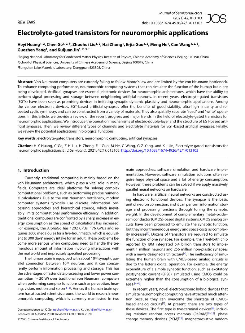
EGTs have two basic operation mechanisms[22], as shownin Fig. 1. The first type is the steady-state (quasi-static) mechan-ism of EDLTs, as shown in Figs. 1(a) and 1(c). When a voltage(VG) lower than the threshold VT is applied at the gate, this res-ults in migration and accumulation of ions at the gate/electro-lyte and semiconductor/electrolyte interfaces. For example,with a positive voltage gate (VG < VT), the anions in the electro-lyte migrate toward the interface of gate electrode/electro-lyte to compensate the charge build up in the gate electrode.Concurrently, on the other side, the cations in the electrolyteaccumulate at the electrolyte/semiconductor interface toform a Helmholtz layer, as shown in Fig. 1(a). The EDLs areonly a few nanometers thick. To balance the formation of theEDL at this interface, electrons (or holes) inside the semicon-ductors accumulate (or deplete) at the solid part of the inter-face, which can be considered as a nanometer-thick capacit-or[27]. Therefore, by varying the applied gate voltage on theelectrolytes, the channel resistance can be controlled by thenumber of charge carriers accumulated at the semiconduct-or side of the interface[28].
In the same way, when a negative voltage gate (|VG| <VT) is applied, the cations in the electrolyte migrate toward
(a)Gate
Electrolyte
S D~1 nm
~1 nm
~1 nm
~1 nm
S D
S D S D
Semiconductor Semiconductor
VG < VT VG > VT
|VG| < VT |VG| > VT
VG
(c)
(b)
(d)
Gate
Gate Gate
Electrolyte
Electrolyte
Semiconductor Semiconductor
Electrolyte
Hole ElectronCation Anion
Fig. 1. (Color online) Schematic of the electrolyte-gated transistor operation mechanisms. (a, c) Quasi-static FET operation and (b, d) electrochemic-al transistors operation. (a) When a positive VG < VT is applied, an EDL is formed at the electrolyte/semiconductor interface (electron doping).(b) When a positive VG > VT is applied, an EDL is formed at the electrolyte/semiconductor interface, but some cations can intercalate into the semi-conductor (electrochemical doping). (c) When a negative VG < VT is applied, an EDL is formed at the electrolyte/semiconductor interface (hole dop-ing). (d) When a negative VG > VT is applied, an EDL is formed at the electrolyte/semiconductor interface but some anions can intercalate into thesemiconductor (electrochemical doping).
2 Journal of Semiconductors doi: 10.1088/1674-4926/42/1/013103
H Y Huang et al.: Electrolyte-gated transistors for neuromorphic applications
the gate electrode/electrolyte interface to compensate thecharge build up in the gate electrode. The anions in theelectrolyte accumulate concurrently at the electrolyte/semi-conductor interface to form a Helmholtz layer, as shown inFig. 1(c). At steady-state, almost all of the applied gate poten-tial is dropped across the double layers and there is ideally anear zero ionic current from the gate to source electrodes.The few- nanometer- thick EDLs can be considered as nano-meter-thick capacitors. The EDL will produce an extremelylarge electric field. Given that the applied of voltage is lowerthan the threshold VT, the electric field force is not enough toinduce ion insert into the semiconductor material, so the ef-fect of the EDL field mechanism is more like the gating effectin the normal field-effect transistor. Once we remove thegate voltage, the EDLs will disappear after few seconds,which corresponds to a volatile memory of channel modula-tion.
The second mechanism is based on electrochemical dop-ing. For the ion permeable semiconductor material, when avoltage (VG) higher than the threshold VT is applied at thegate, because of the giant EDL effect, small ions such asH+[29], Li+[30], and O2–[31, 32] can be inserted into the channeland change its doping level, thus controlling the conduct-ance of the channel. As shown in Figs. 1(b) and 1(d), this is aprocess of electrochemical doping. An electrochemical transist-or can realize reversible electrochemical doping and anti-dop-ing (reversible oxidation and reduction reaction) by applica-tion of different gate biases. In general, electrochemical dop-ing induces reversible structural changes, such as SrCoOx
[32],SrFeOx
[31], WO3[29], VO2
[33] and so on, which corresponds tothe nonvolatile memory of channel modulation.
In this case, a positive VG larger than VT is initially ap-plied; the small cations are accumulated at the semiconduct-or’s interface forming a strong EDL field and are then injec-ted into the semiconductor, as shown in Fig. 1(b). After apply-ing a negative gate voltage, cations are extracted from thesemiconductor channel and de-doping of the semiconductoroccurs, resulting in the semiconductor conductance return-ing to its initial state. Similarly, if a negative VG larger than VT
is applied, the small anions are accumulated at the semicon-ductor’s interface forming a strong EDL field and are then injec-ted into the semiconductors, as shown in Fig. 1(d). After apply-ing a positive gate voltage, anions are extracted from the se-miconductor channel and the semiconductor is de-doped.
3. EGT-based artificial synapses
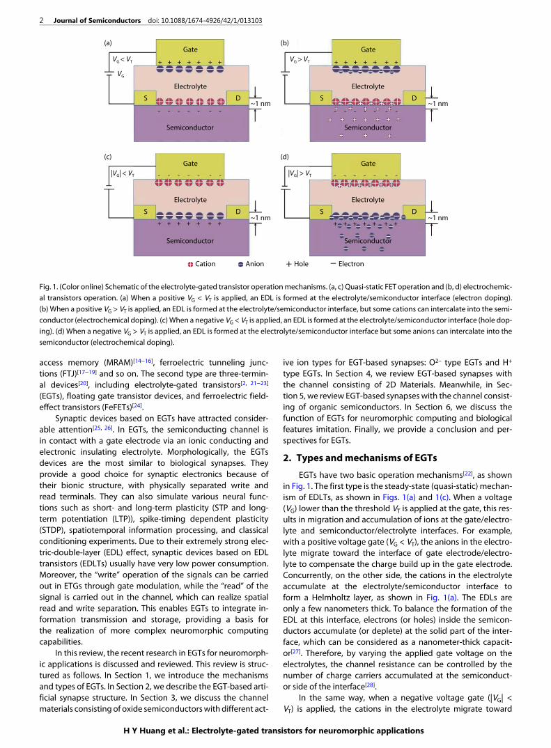
Synapses are the essential units for learning and memoryin neural networks. Fig. 2(a) shows a schematic diagram of bio-logical synapses, which consist of three parts: the presyn-aptic neuron, the synaptic cleft, and the postsynaptic neuron.In biological synapses, information transmission and pro-cessing are complex processes. When the synaptic action po-tential arrives at the presynaptic terminal through the axon, itcan trigger the pre-synapse to release to the synaptic cleft aneurotransmitter, such as Ca+, Na+, K+, and Cl–, which is heldin the synaptic vesicles before the arrival of the presynaptic ac-tion potential. The neurotransmitter diffuses through the syn-aptic cleft and binds to the receptor proteins on the postsyn-aptic membrane[1]. Depending on the type of receptor on thepostsynaptic membrane, there are two types of synapses: excit-atory and inhibitory. The excitatory synapses lead to the excit-atory postsynaptic potential/current (EPSP/EPSC) and drivethe postsynaptic neuron to generate an action potential. Theinhibitory synapses result in the inhibitory postsynaptic poten-tial/current (IPSP/IPSC) and prevent the postsynaptic neuronfrom generating an action potential. The synaptic weight,which is the connection strength between neurons, can bechanged by either or both sides of the synapse. This is re-ferred to as “synaptic plasticity.” The synaptic plasticity canbe classified into STP and LTP by the retention time. STP re-tains only milliseconds to minutes, which consists of the funda-mental computational functions in neural networks. LTP re-tains several hours or longer, which consists of fundamentalmemory functions in neural network, so that the brain canstore a lot of information. Synaptic weights can be simulatedby the temporal relationship between presynaptic and post-synaptic spikes, which is called spike-timing-dependent plasti-
VPre-synaptic
IPost
Gate
Pre-synaptic
Synaptic EGTs
Post-synaptic
Electrolyte
Semiconductor
S D
(b)
Pre-synapticneuron
Post-synapticneuron
Synapse
Input(a)
Output
Vesicies
EPSP/IPSP
Ca2+
Na+
Ca2+Cl−
Act
ion
po
ten
tial
Excitatory/inhibitory
Neurotransmitter
K+
Fig. 2. (Color online) (a) Schematic of a biological synapse[34] and (b) an EGT-based artificial synapse. The synaptic weight (channel conductance)can be modulated in this device using electrochemical intercalation to adjust the small ion concentration in the semiconductor.
Journal of Semiconductors doi: 10.1088/1674-4926/42/1/013103 3
H Y Huang et al.: Electrolyte-gated transistors for neuromorphic applications
city (STDP)[2].In recent years, more and more researchers have ex-
ploited the EGTs to simulate synaptic function. Electrolytesare ionic conductors, but they are electronic insulators. Theelectrolyte can be either liquid or solid, and the ions (anionsand cations) in the electrolyte are distributed in the two inter-faces with opposite charges under the action of an electricfield. EGTs use ions in the electrolyte layer to effectively regu-late the electrical conductivity of the device channel.
Thee migration of ions in an electrolyte under the influ-ence of the gate voltage is like the release of neurotransmit-ters. As shown in Fig. 2(b), similar to biological synapses, thegate electrode of EGTs can be considered to be a presyn-aptic neuron, the electrolyte is like the synaptic cleft, and thesemiconductor channel as a postsynaptic neuron, so the chan-nel conductivity is the equivalent of the synaptic weight. Asmentioned earlier, EGTs work in two basic modes: electrostat-ic modulation and electrochemical doping. When the EGT op-erates in an electrostatic state, the resulting channel conduct-ance changes can be automatically recovered, providing abasis for modeling STP. When the EGT is in electrochemicaldoping mode, the channel conductance changes are nonvolat-ile, which provides the basis for the simulation of LTP, andhas nonvolatile and multi-state memory functions. For a bio-logically synaptic event, the energy consumption is about10–15 J per pulse. The low energy consumption characterist-ics of EGTs also allow them to function as ultra-low-energy syn-aptic devices. Moreover, the “write” operation of signals canbe carried out in ETGs through gate modulation, while the“read” of signal transmission lies in the channel’s function; soan EGT can realize spatial read and write separation. This en-ables EGTs to integrate information transmission and storageat the same time, providing a basis for the realization of morecomplex neuromorphic functions.
Different channel materials have been investigated in elec-trolyte-gated synaptic transistors. Moreover, due to the com-plexity of ion dynamics, ion regulation can be carried out bystimulating the gate with different voltage characteristics,such as pulse width, pulse frequency, and voltage polarity.Channel materials can consist of the following categories:complex metal oxides (e.g., SmNiO3
[21], SrCoOx[32], SrFeOx
[31],VO2
[33]); one-dimensional materials (e.g. carbon nano-tube[35, 36]); two-dimensional materials (e.g. graphene[37],TDMs[38]); and organic materials (e.g. cellulose[39], organic car-bon nanotubes[40], etc.). The most common classes of electro-lytes consist of polymer electrolytes[41−43] [(PEO)/LiClO4
[44],(PSSH)[45] and P(VPA-AA)[43]], ionic liquids[46−50] and ionicgels[51−56], inorganic solid-state electrolytes, and so on. Fromthe type of functional ions, the EGTs can be divided intoO2–[31, 32], H+[29], Ag+[57], Na+[58, 59] and Li+[60] types. Under avery large electric field, ions can diffuse into the channel mater-ial. In the next part we will discuss several ion types for EGTs.
4. Channel materials with oxide semiconductors
4.1. Channel materials with oxide semiconductors: O2−-
EGTs
Oxygen ions can be used as functional ions in high-per-formance electrolyte synaptic transistors[61−63]. In ionic liquid(IL)-gated transistors, the channel can be regarded as a biolo-gical postsynaptic neuron and the gate terminal can be re-
garded as a presynaptic neuron. The water molecules contam-inated in ILs can dissociate into H+ and OH– under high gatevoltages[29]. Because of the EDL effect, functional ions can beinserted into the channel materials through gating. This pro-cess is an electrochemical transistor operation.
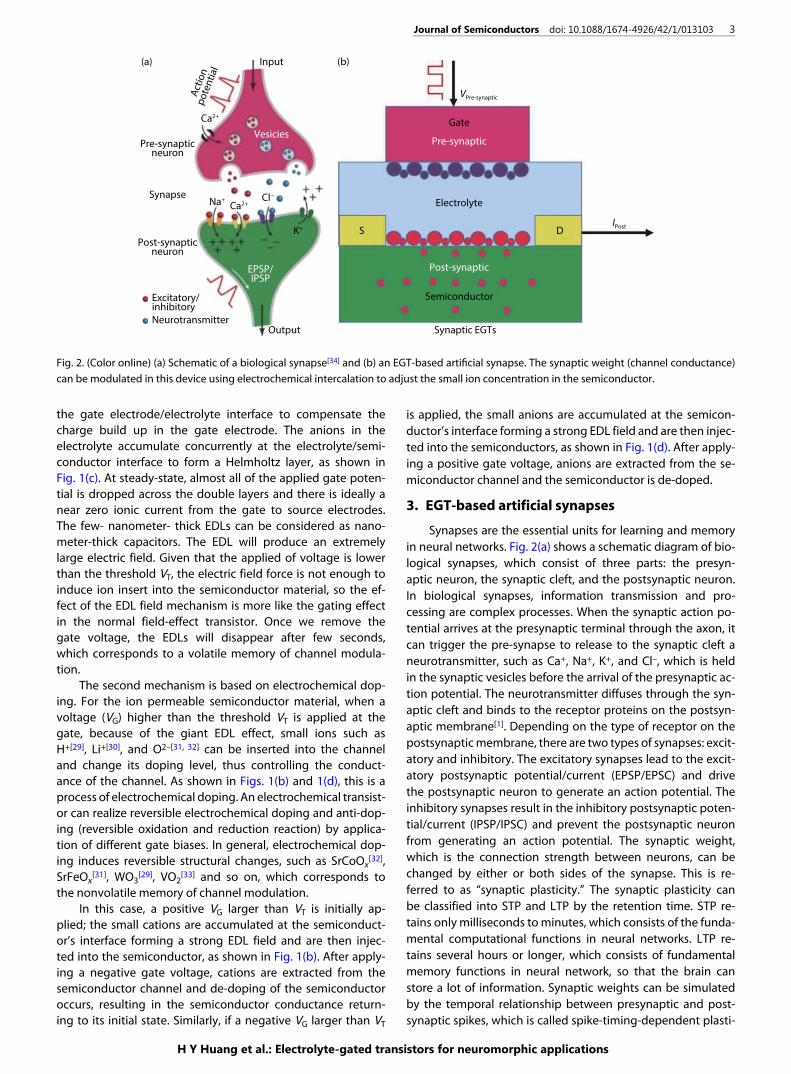
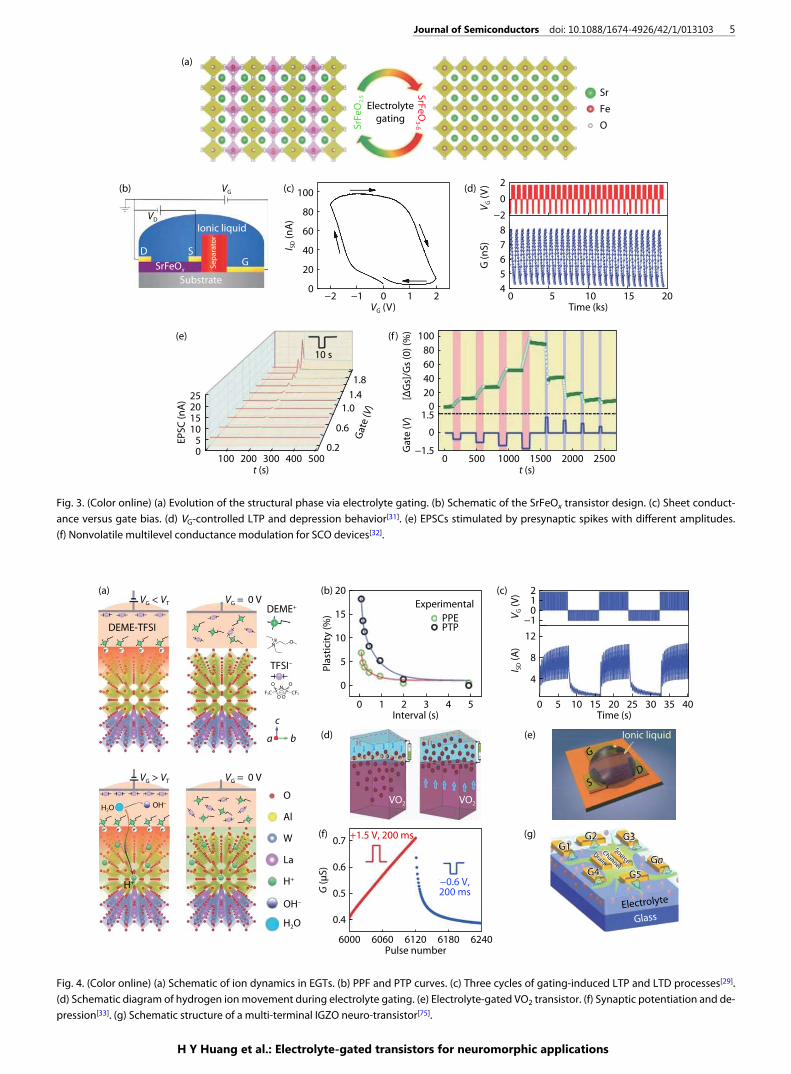
The conductivity of some oxides is very sensitive to oxy-gen content, and several oxides such as SrFeOx (SFO) under-go topotactic phase transition by controlling redox reacti-ons[31]; as shown in Fig. 3(a). In addition, the oxygen contentof those oxides can be controlled by using electrolyte gating,which offers many opportunities for designing artificial syn-aptic transistors. A SFO synaptic transistor is shown inFig. 3(b). The structure of the channel can be controlled revers-ibly between the insulating brownmillerite (BM) and conduct-ive perovskite (PV) phases. The transfer curves show a clock-wise hysteresis loop in Fig. 3(c). The negative voltage pulses in-duce the insertion of oxygen ions into the BM-SFO channel,leading to phase transformation from BM-SFO to PV-SFO. Incontrast, positive gate pulses can induce the oxygen ion extrac-tion from the channel, thus inducing phase transformationfrom PV-SFO to BM-SFO. Long-time plasticity is related tomemory function in human brain, which consists of LTP andlong-term depression (LTD) correspond to strengthening andweakening of synaptic weight. They are still stable after afew minutes to several years. As shown in Fig. 3(d), LTP andLTD behaviors are realized in SFO EGTs by applying 16 consec-utive negative pulses (−1.8 V for 5 s, spaced 10 s apart) and24 consecutive positive pulses (1.8 V for 10 s, spaced 10 sapart). Similarly, the same group designed the EGTs usingSrCoOx (SCO)[32]. The EPSCs were induced by presynapticspikes with different amplitudes in SCO devices, as shown inFig. 3(e), and the conductance modulation is nonvolatile multi-level (Fig. 3(f)). This process further demonstrated the nonvolat-ile properties of SCO-based devices.
Shi et al. demonstrated a liquid electrolyte-gated correl-ated nickelate (SmNiO3) synaptic transistor with oxygenions[21]. Applying a negative pulse sequence on the gate elec-trode increases the conductance of SmNiO3, while applying apositive pulse sequence decreases its conductivity. Owing tothis property, asymmetric and symmetric STDP simulationshave been achieved.
4.2. Channel materials with oxide semiconductors: H+-
EGTs
Protons are the smallest-sized cations that exist in a widerange of solid[64−71] and liquid[72, 73] electrolytes. Due to thelow weight and small volume of protons, they can be usedas functional ions in electrolyte synaptic transistors. By gat-ing-induced protonation and deprotonation, one can realizereversible phase transformations between various H+ dopedphases. Recently, WO3
[29] and VO2[33] have been exploited as
channel layers for proton-based synaptic transistors.Yang et al. reported an IL gated EGTs using a WO3 chan-
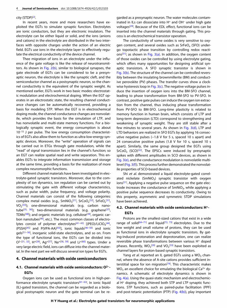
nel, where the absence of A-site cations provides sufficient in-terstitial space for ion migration[74]. This characteristic makesWO3 an excellent choice for emulating the biological Ca2+ dy-namics. A schematic of electrolyte dynamics is shown inFig. 4(a). Using the quasi-static mechanism and electrochemic-al H+ doping, they achieved both STP and LTP synaptic func-tions. STP functions, such as paired-pulse facilitation (PPF)and post-tetanic potentiation (PTP) (Fig. 4(b)), play important
4 Journal of Semiconductors doi: 10.1088/1674-4926/42/1/013103
H Y Huang et al.: Electrolyte-gated transistors for neuromorphic applications
Electrolyte
gating
(a)
SrF
eO
2.5
SrF
eO
3-δ
Sr
Fe
O
VG
VD
D SG
(b)
Ionic liquid
Substrate
SrFeOx
Se
pa
rato
r
(c)
80
100
−20
20
40
60
−1 0VG (V)
I SD (
nA
)1 2
(d)
04
5
6
8
7
5 10Time (ks)
G (
nS
)
15 20
−2
0
2
VG (
V)
(e)
10 s
25201510
EP
SC
(n
A)
t (s)
Gat
e (V
)
50
100 200 300 400 5000.2
0.6
1.0
1.4
1.8
t (s)
Ga
te (V
)[Δ
Gs]
/Gs
(0)
(%)
0 500
0
0
20
40
60
80
100
1.5
−1.51000 1500 2000 2500
(f )
Fig. 3. (Color online) (a) Evolution of the structural phase via electrolyte gating. (b) Schematic of the SrFeOx transistor design. (c) Sheet conduct-ance versus gate bias. (d) VG-controlled LTP and depression behavior[31]. (e) EPSCs stimulated by presynaptic spikes with different amplitudes.(f) Nonvolatile multilevel conductance modulation for SCO devices[32].
VG < VT VG = 0 V
DEME-TFSI
(a)
a b
c
TFSI−
F3C CF3
O O
ON−S S
O
DEME+
NO
e+ e+ e+
VG > VT
H2O OH−
VG = 0 V
O
Al
W
La
H+
OH−
H2O
e+ e+ e+
H+
e+ e+
e+
G5
Drain
Channel
Source
G4
G1G2 G3
Gn
0
0
5
10
15
20
1 2Interval (s)
Experimental
PPEPTP
Pla
stic
ity
(%)
3 4 5
(b)
VO2 VO2
(d)
6000
0.4
0.5
0.6
0.7
6060 6120Pulse number
G (
μS
)
6180
+1.5 V, 200 ms
−0.6 V,200 ms
6240
(f)
0 5
4
8
12
−1
210
10 15 25 40Time (s)
Ionic liquid
S
D
G
VG (
V)
I SD (
A)
20 30 35
(c)
(e)
(g)
Electrolyte
Glass
G5
Drain
Channel
Source
G4
G1G2 G3
Gn
Fig. 4. (Color online) (a) Schematic of ion dynamics in EGTs. (b) PPF and PTP curves. (c) Three cycles of gating-induced LTP and LTD processes[29].(d) Schematic diagram of hydrogen ion movement during electrolyte gating. (e) Electrolyte-gated VO2 transistor. (f) Synaptic potentiation and de-pression[33]. (g) Schematic structure of a multi-terminal IGZO neuro-transistor[75].
Journal of Semiconductors doi: 10.1088/1674-4926/42/1/013103 5
H Y Huang et al.: Electrolyte-gated transistors for neuromorphic applications
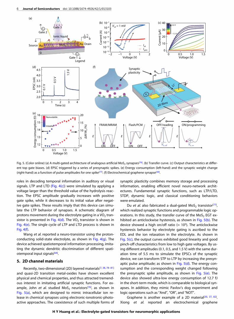
roles in decoding temporal information in auditory or visualsignals. LTP and LTD (Fig. 4(c)) were simulated by applying avoltage larger than the threshold value of the hydrolysis reac-tion. The EPSC amplitude gradually increases with positivegate spike, while it decreases to its initial value after negat-ive gate spikes. These results imply that this device can simu-late the LTP behavior of synapses. A schematic diagram ofprotons movement during the electrolyte gating in a VO2 tran-sistor is presented in Fig. 4(d). The VO2 transistor is shown inFig. 4(e). The single cycle of LTP and LTD process is shown inFig. 4(f).
Wang et al. reported a neuro-transistor using the proton-conducting solid-state electrolyte, as shown in Fig. 4(g). Thedevice achieved spatiotemporal information processing, imita-ting the dynamic dendritic discrimination of different spati-otemporal input signals[64].
5. 2D channel materials
Recently, two-dimensional (2D) layered materials[7, 38, 78−81]
and quasi-2D transition metal-oxides have shown excellentphysical and chemical properties, and thus attracted tremend-ous interest in imitating artificial synaptic functions. For ex-ample, John et al. studied MoS2 neuristors[76], as shown inFig. 5(a), which are designed to mimic intracellular ion re-lease in chemical synapses using electronic-ionotronic-photo-active approaches. The coexistence of such multiple forms of
synaptic plasticity combines memory storage and processinginformation, enabling efficient novel neuro-network archit-ectures. Fundamental synaptic functions, such as LTP/LTD,STDP, dynamic logic, and classical conditioning behaviorswere emulated.
Du et al. also fabricated a dual-gated MoS2 transistor[77],which realized synaptic functions and programmable logic op-erations. In this study, the transfer curve of the MoS2 EGT ex-hibited an anticlockwise hysteresis, as shown in Fig. 5(b). Thedevice showed a high on/off ratio (≈ 105). The anticlockwisehysteresis behavior by electrolyte gating is ascribed to theEDL and the ion relaxation in the electrolyte. As shown inFig. 5(c), the output curves exhibited good linearity and goodpinch-off characteristics from low to high gate voltages. By us-ing different amplitudes (0.1, 0.5, and 1.5 V) with the same dur-ation time of 5.5 ms to simulate the EPSCs of the synapticdevice, we can transform STP to LTP by increasing the presyn-aptic pulse amplitude; as shown in Fig. 5(d). The energy con-sumption and the corresponding weight changed followingthe presynaptic spike amplitude, as shown in Fig. 5(e). Thedevice also showed ultra-low energy consumption of 12.7 fJin the short-term mode, which is comparable to biological syn-apses. In addition, they mimic Pavlov’s dog experiment andlogic operations such as “And”, “OR”, and “NOT”.
Graphene is another example of a 2D material[30, 37, 82].Xiong et al. reported an electrochemical graphene
VG2
Gate 2
Gate 1Legend
DrainSource
Gate 3
(a)
Ionic liquid
VG1
I0 VD
A
MoS2
SiO2
Si
AuAu
−2 −110−13
10−12
10−11
10−10
10−9
10−8
10−7(b)
0Voltage (V)
Vsd = 1 mV
Isd
Igate
Cu
rre
nt
(A)
1 2 0 0.5
2.6 V
−1.5 V
1.0Voltage (V)
1.5
10
0
20
30
40(c)
Cu
rre
nt
(μA
)
0
2.0
2.5
3.0
3.5
4.0
4.5
1 2Time (s)
0.1
V
0.5
V
1.5
V(d)
EP
SC
(n
A)
3 4
0 0.5Voltage (V)
Nonvolatile
Volatile
ΔW
/W0 (
%)
0
5
10
15
20
En
erg
y co
nsu
mp
tio
n (
fJ)
12
13
14
15
16(e)
1.0 1.5
Synaptic
plasticity
E
FRAM/MRAM Flash/PCM OFF/reading ON/programming
Vb, off Vb, onON OFF ON OFF
E E E
V
2D films
Reference
Li+
(f)
Fig. 5. (Color online) (a) A multi-gated architecture of analogous artificial MoS2 synapses[76]. (b) Transfer curve. (c) Output characteristics at differ-ent top gate biases. (d) EPSC triggered by a series of presynaptic spikes. (e) Energy consumption (left-hand) and the synaptic weight change(right-hand) as a function of pulse amplitudes for one spike[77]. (f) Electrochemical graphene synapse[30].
6 Journal of Semiconductors doi: 10.1088/1674-4926/42/1/013103
H Y Huang et al.: Electrolyte-gated transistors for neuromorphic applications
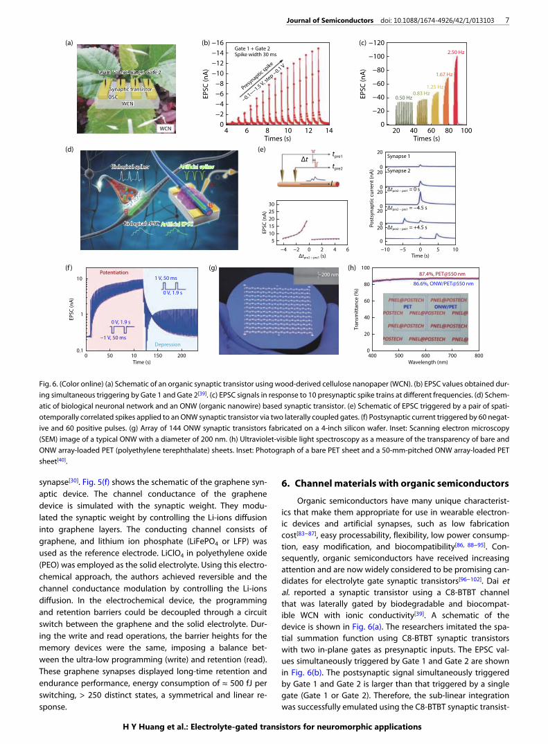
synapse[30]. Fig. 5(f) shows the schematic of the graphene syn-aptic device. The channel conductance of the graphenedevice is simulated with the synaptic weight. They modu-lated the synaptic weight by controlling the Li-ions diffusioninto graphene layers. The conducting channel consists ofgraphene, and lithium ion phosphate (LiFePO4 or LFP) wasused as the reference electrode. LiClO4 in polyethylene oxide(PEO) was employed as the solid electrolyte. Using this electro-chemical approach, the authors achieved reversible and thechannel conductance modulation by controlling the Li-ionsdiffusion. In the electrochemical device, the programmingand retention barriers could be decoupled through a circuitswitch between the graphene and the solid electrolyte. Dur-ing the write and read operations, the barrier heights for thememory devices were the same, imposing a balance bet-ween the ultra-low programming (write) and retention (read).These graphene synapses displayed long-time retention andendurance performance, energy consumption of ≈ 500 fJ perswitching, > 250 distinct states, a symmetrical and linear re-sponse.
6. Channel materials with organic semiconductors
Organic semiconductors have many unique characterist-ics that make them appropriate for use in wearable electron-ic devices and artificial synapses, such as low fabricationcost[83−87], easy processability, flexibility, low power consump-tion, easy modification, and biocompatibility[86, 88−95]. Con-sequently, organic semiconductors have received increasingattention and are now widely considered to be promising can-didates for electrolyte gate synaptic transistors[96−102]. Dai etal. reported a synaptic transistor using a C8-BTBT channelthat was laterally gated by biodegradable and biocompat-ible WCN with ionic conductivity[39]. A schematic of thedevice is shown in Fig. 6(a). The researchers imitated the spa-tial summation function using C8-BTBT synaptic transistorswith two in-plane gates as presynaptic inputs. The EPSC val-ues simultaneously triggered by Gate 1 and Gate 2 are shownin Fig. 6(b). The postsynaptic signal simultaneously triggeredby Gate 1 and Gate 2 is larger than that triggered by a singlegate (Gate 1 or Gate 2). Therefore, the sub-linear integrationwas successfully emulated using the C8-BTBT synaptic transist-
0
−2
−4
−6
4 6 8 10
Gate 1 + Gate 2Spike width 30 ms
−0.1~−1.5 V, ste
p −0.1 V
Presy
naptic sp
ike
12 14
−8
−10
−12
EP
SC
(n
A)
Times (s)
−14
−16(b)
0
−20
20 6040 80
0.50 Hz0.83 Hz
1.25 Hz
1.67 Hz
2.50 Hz
100
−40
−60
−80
EP
SC
(n
A)
Times (s)
−100
−120(c)
(g)
(d)
Biological spikes
Biological EPSC
Artificial spikes
Artificial EPSC
(a)
Drain Source
Synaptic transistor
OSC
WCN
Gate 1 Gate 2
WCN
~200 nm(f )
10
1
0.10 50 10
Time (s)
Potentiation
Depression
1 V, 50 ms
−1 V, 50 ms
0 V, 1.9 s
0 V, 1.9 s
150 200
EP
SC
(n
A)
−10
0
200
200
20
Po
stsy
na
pti
c cu
rre
nt
(nA
)
0
20
20Synapse 1
Synapse 2
Δtpre2 − pre1 = 0 s
Δtpre2 − pre1 = −4.5 s
Δtpre2 − pre1 = +4.5 s
0
−5 0Time (s)
5 10
(e)
Δttpre1
tpre2
I
Δtpre2 − pre1 (s)
30
25
20
EP
SC
(n
A)
15
−4 −2 0 2 4 6
10
5
(h) 10087.4%, PET@550 nm
86.6%, ONW/PET@550 nm80
60
40
20
0400 500
Wavelength (nm)
700600 800Tr
an
smit
tan
ce (
%)
Fig. 6. (Color online) (a) Schematic of an organic synaptic transistor using wood-derived cellulose nanopaper (WCN). (b) EPSC values obtained dur-ing simultaneous triggering by Gate 1 and Gate 2[39]. (c) EPSC signals in response to 10 presynaptic spike trains at different frequencies. (d) Schem-atic of biological neuronal network and an ONW (organic nanowire) based synaptic transistor. (e) Schematic of EPSC triggered by a pair of spati-otemporally correlated spikes applied to an ONW synaptic transistor via two laterally coupled gates. (f) Postsynaptic current triggered by 60 negat-ive and 60 positive pulses. (g) Array of 144 ONW synaptic transistors fabricated on a 4-inch silicon wafer. Inset: Scanning electron microscopy(SEM) image of a typical ONW with a diameter of 200 nm. (h) Ultraviolet-visible light spectroscopy as a measure of the transparency of bare andONW array-loaded PET (polyethylene terephthalate) sheets. Inset: Photograph of a bare PET sheet and a 50-mm-pitched ONW array-loaded PETsheet[40].
Journal of Semiconductors doi: 10.1088/1674-4926/42/1/013103 7
H Y Huang et al.: Electrolyte-gated transistors for neuromorphic applications
ors with dual in-plane gates. The signal filtering characterist-ics and dendritic integration were simulated in laterallycoupled field-effect transistors (LCFETs), as shown in Fig. 6(c).With the increase of presynaptic spike frequency, the EPSCamplitude increased dramatically.
Xu et al. designed a synaptic transistor-based on organicnanowires (ONW)[40], as shown in Fig. 6(d), to emulate the func-tions of a biological synapse. They demonstrated basic spati-otemporal dynamic logic with two laterally coupled gates, asshown in Fig. 6(e). The imitation of LTP and LTD are shown inFig. 6(f). As shown in Fig. 6(g), 144 large-scale synaptic transist-ors were fabricated on a 4-inch wafer using highly aligned ON-Ws. The photograph in Fig. 6(h) showed no obvious reduc-tion in the transparency of PET (polyethylene terephthalate)by the ONW coverage. With a core-sheath-structured ONW act-ive channel and a well-confined 300-nm channel length ob-tained using ONW lithography, ~1.23 fJ per synaptic eventfor individual ONW was attained, which rivals that of biologic-al synapses.
7. The function of EGTs for neuromorphiccomputing and biological features imitation
7.1. EGTs for neuromorphic computing
STDP is essential to emulate a synaptic plasticity mec-hanism in the neural network[2, 29]. By changing the shapeof the preneuron spike waveform, we achieved the asymmet-ric and symmetric STDP function in SFO EGTs[31] as shown inFig. 7(a). The SFO EGTs accomplishes the function of handwrit-ten digits recognition as shown in Fig. 7(b). The image recogni-tion accuracy has been calculated using the conductancestates in LTP and LTD processes to perform supervised learn-ing with back-propagation of two standard digital, a 8 × 8
pixels of handwritten digits from the “Optical Recognition ofHandwritten Digits” dataset (the accuracy approaches 95.2%after 16 training epochs) and 28 × 28 pixels of handwritten di-gits from Modified National Institute of Standards and Techno-logy (MNIST) dataset (the accuracy approaches 92.7%).
Logic operations are meaningful to computation perform-ance in a neural network. Du et al. demonstrated that a dual-gated MoS2 transistor can simulate a logic operation such as“AND”, “OR”, and “NOT” operations[77], as shown in Fig. 7(c).Gate 1 (electrolyte gate) and the Gate 2 (back gate) were re-garded as two input terminals, while the drain was used forthe output terminal. By regulating the conductance state, wecan reversibly transform “AND” logic into “OR” logic. We canalso manipulate the amplitude of voltage Gate 2 pulses to sim-ulate “NOT” logic.
7.2. EGTs for emulating biological functions
Recently, researchers have made remarkable process in im-itating functionalities of the biological nervous system, suchas artificial sensory nerves, spatiotemporal information pro-cessing, neural emulation, orientation tuning inartificial neur-ons, the famous classical conditioning of Pavlov’s dog experi-ments and others. As shown in Fig. 8(a), Kim et al. designed aflexible organic electronics system to simulate an artificialnerve[95]. The artificial afferent nerve consisted of three funda-mental components, as shown in Fig. 8(a): (i) pressuresensors, (ii) organic ring oscillators, and (iii) a synaptic transist-or. The system simulates the function of a hybrid bioelectron-ic reflex and consists of two parts: the first uses the multipletactile receptors to collecting data, the second conveys this in-formation to biological efferent nerves. Multiple tactile recept-ors are utilized to convert external tactile stimuli into electric-al signals. An ion gel-gated synaptic transistor was integ-
(a)
Drain
Gate output
Pre-spike
Post-spike
Source
Multiplexer
784 inputneurons
MNISTimages
28 × 28pixels
Weights Weights
300 hiddenneurons
10 outputneurons
15
10
5
0
−5
−10
−150
Δt (s)
ΔW
(%
)
200 400 600−200−400−600
Symmetric STDP
15
10
5
0
−5
−10
−150
Δt (s)
ΔW
(%
)
200 400 600−200−400−600
Asymmetric STDP
+1.4 V
20 s
Post-spike
Vp
ost (
V)
Vp
re (
V)
Pre-spike210
−1−2
−600 −400 −200 0 200 400 600
2
1
0
Δt (s)
08
12
16
20
92
96
100
Acc
ura
cy
(%
)
10 20 30Training epoch
40
Large digitsSFONumeric
Gate 1
1.6 VAND OR
Eout
Gate 2
6 ms
−1.2 V 6 ms
EoutGate2
High input voltage
NOT
08
12
16
20
92
96
100
Acc
ura
cy
(%
)
10 20 30Training epoch
40
Small digitsSFONumeric
Programmingpulses
Synaptictransistor
Read output
Re
ad
pu
lse
s
Accessdevice
w11 w12 w13
w21 w22 w23
w31 w32 w33
(c)
(b)
Fig. 7. (Color online) (a) Asymmetric and symmetric STDP functions implemented in ferrite synaptic transistors. (b) Neuromorphic computing simu-lation[31]. (c) Configurable logic operations with dual gating[77].
8 Journal of Semiconductors doi: 10.1088/1674-4926/42/1/013103
H Y Huang et al.: Electrolyte-gated transistors for neuromorphic applications
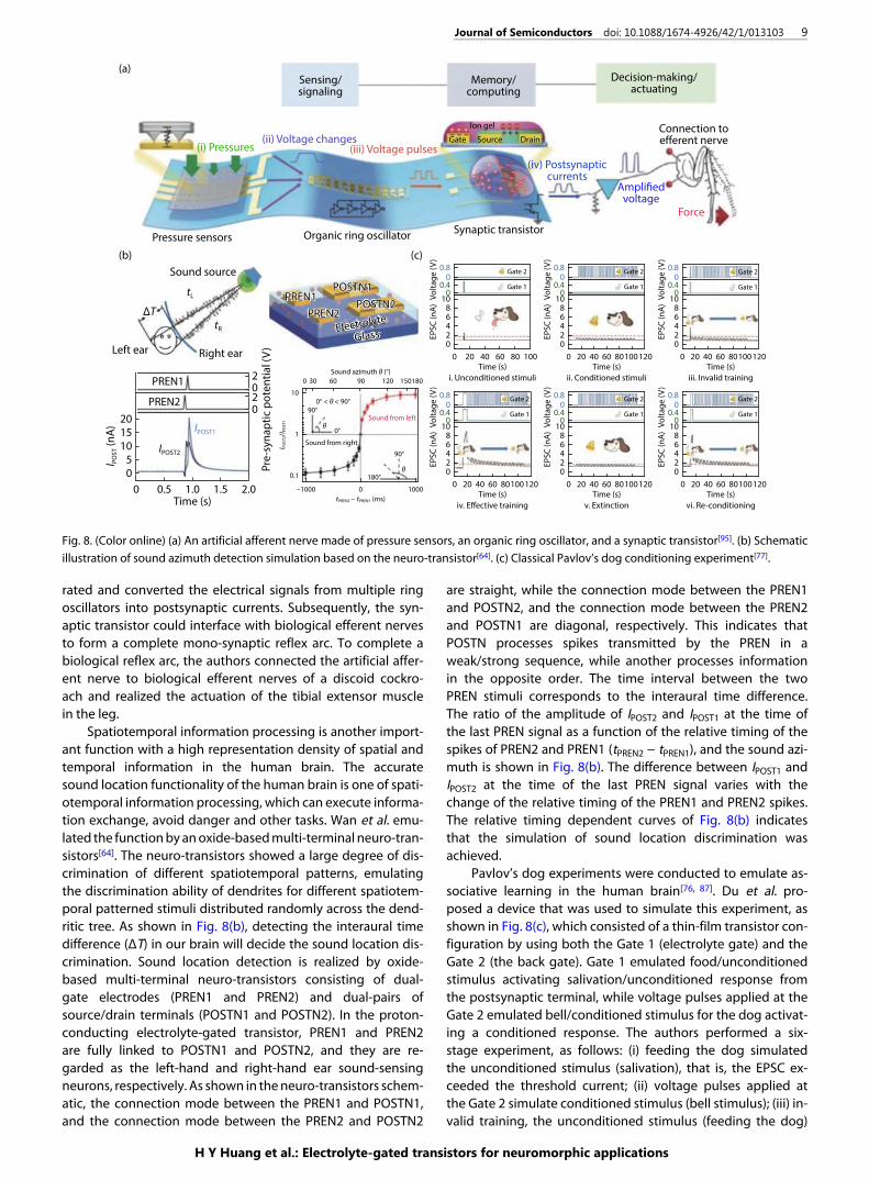
rated and converted the electrical signals from multiple ringoscillators into postsynaptic currents. Subsequently, the syn-aptic transistor could interface with biological efferent nervesto form a complete mono-synaptic reflex arc. To complete abiological reflex arc, the authors connected the artificial affer-ent nerve to biological efferent nerves of a discoid cockro-ach and realized the actuation of the tibial extensor musclein the leg.
Spatiotemporal information processing is another import-ant function with a high representation density of spatial andtemporal information in the human brain. The accuratesound location functionality of the human brain is one of spati-otemporal information processing, which can execute informa-tion exchange, avoid danger and other tasks. Wan et al. emu-lated the function by an oxide-based multi-terminal neuro-tran-sistors[64]. The neuro-transistors showed a large degree of dis-crimination of different spatiotemporal patterns, emulatingthe discrimination ability of dendrites for different spatiotem-poral patterned stimuli distributed randomly across the dend-ritic tree. As shown in Fig. 8(b), detecting the interaural timedifference (ΔT) in our brain will decide the sound location dis-crimination. Sound location detection is realized by oxide-based multi-terminal neuro-transistors consisting of dual-gate electrodes (PREN1 and PREN2) and dual-pairs ofsource/drain terminals (POSTN1 and POSTN2). In the proton-conducting electrolyte-gated transistor, PREN1 and PREN2are fully linked to POSTN1 and POSTN2, and they are re-garded as the left-hand and right-hand ear sound-sensingneurons, respectively. As shown in the neuro-transistors schem-atic, the connection mode between the PREN1 and POSTN1,and the connection mode between the PREN2 and POSTN2
are straight, while the connection mode between the PREN1and POSTN2, and the connection mode between the PREN2and POSTN1 are diagonal, respectively. This indicates thatPOSTN processes spikes transmitted by the PREN in aweak/strong sequence, while another processes informationin the opposite order. The time interval between the twoPREN stimuli corresponds to the interaural time difference.The ratio of the amplitude of IPOST2 and IPOST1 at the time ofthe last PREN signal as a function of the relative timing of thespikes of PREN2 and PREN1 (tPREN2 − tPREN1), and the sound azi-muth is shown in Fig. 8(b). The difference between IPOST1 andIPOST2 at the time of the last PREN signal varies with thechange of the relative timing of the PREN1 and PREN2 spikes.The relative timing dependent curves of Fig. 8(b) indicatesthat the simulation of sound location discrimination wasachieved.
Pavlov’s dog experiments were conducted to emulate as-sociative learning in the human brain[76, 87]. Du et al. pro-posed a device that was used to simulate this experiment, asshown in Fig. 8(c), which consisted of a thin-film transistor con-figuration by using both the Gate 1 (electrolyte gate) and theGate 2 (the back gate). Gate 1 emulated food/unconditionedstimulus activating salivation/unconditioned response fromthe postsynaptic terminal, while voltage pulses applied at theGate 2 emulated bell/conditioned stimulus for the dog activat-ing a conditioned response. The authors performed a six-stage experiment, as follows: (i) feeding the dog simulatedthe unconditioned stimulus (salivation), that is, the EPSC ex-ceeded the threshold current; (ii) voltage pulses applied atthe Gate 2 simulate conditioned stimulus (bell stimulus); (iii) in-valid training, the unconditioned stimulus (feeding the dog)
Sensing/signaling
Memory/computing
Decision-making/actuating
Pressure sensors Organic ring oscillatorSynaptic transistor
(iv) Postsynapticcurrents
Amplifiedvoltage
Force
(i) Pressures(ii) Voltage changes
(iii) Voltage pulsesGate Source Drain
Ion gel Connection toefferent nerve
(a)
(b) (c)
PREN1
PREN2
POSTN1
POSTN2
Electrolyte
Glass
Sound source
Right earLeft ear
ΔT
tL
tR
0.80
0.40
10
EP
SC
(n
A)
Vo
lta
ge
(V
)
86420
0 20 40 60Time (s)
i. Unconditioned stimuli
80
Gate 2
Gate 1
100
0.80
0.40
10
EP
SC
(n
A)
Vo
lta
ge
(V
)
86420
0 20 40 60Time (s)
ii. Conditioned stimuli
80 120100
Gate 2
Gate 1
IPOST2
PREN2
PREN1
IPOST1
0 0.5 1.0
05
101520
2020
I PO
ST (
nA
)
Pre
-syn
ap
tic
po
ten
tia
l (V
)
Time (s)1.5 2.0
tPREN2 − tPREN1 (ms)
0.1
1
−1000 1000
0 90
Sound azimuth θ (°)
1801501206030
0
10
I PO
ST
2/I
PO
ST
1
Sound from left
Sound from right
90°
90°
180°
0° < θ < 90°
0°θ
θ
0.80
0.40
10E
PS
C (
nA
)V
olt
ag
e (
V)
86420
Time (s)
iv. Effective training
Gate 2
Gate 1
0 20 40 60 80 120100
0.80
0.40
10
EP
SC
(n
A)
Vo
lta
ge
(V
)
86420
Time (s)
v. Extinction
Gate 2
Gate 1
0 20 40 60 80 120100
0.80
0.40
10
EP
SC
(n
A)
Vo
lta
ge
(V
)
86420
Time (s)
vi. Re-conditioning
Gate 2
Gate 1
0 20 40 60 80 120100
0.80
0.40
10
EP
SC
(n
A)
Vo
lta
ge
(V
)
86420
Time (s)
iii. Invalid training
Gate 2
Gate 1
0 20 40 60 80 120100
Fig. 8. (Color online) (a) An artificial afferent nerve made of pressure sensors, an organic ring oscillator, and a synaptic transistor[95]. (b) Schematicillustration of sound azimuth detection simulation based on the neuro-transistor[64]. (c) Classical Pavlov’s dog conditioning experiment[77].
Journal of Semiconductors doi: 10.1088/1674-4926/42/1/013103 9
H Y Huang et al.: Electrolyte-gated transistors for neuromorphic applications
and conditioned stimulus (bell stimulus) did not respond by ashort time training; (iv) effect train, when the period of time in-creased to 10 s, the connection between unconditioned stimu-lus (feeding the dog) and conditioned stimulus (bell stimulus)was strengthened, after which the dog’s salivation could bestimulated by a conditioned stimulus; (v) forgetting, without re-peated training with simultaneous unconditioned and condi-tioned stimulus, the conditioned response would graduallydisappear; and (vi) re-conditioning: the connection was re-stored by applying a shorter time training[77].
8. Conclusion and perspectives
In summary, we provide a review of the recent progressand major trends in the field of EGTs for neuromorphic applica-tions. In the beginning, we introduced two basic operationmechanisms of EDLs: 1) the quasi-static mechanism, and 2)the electrochemical doping mechanism. We introduced thestructure of EGT-based artificial synapses and the basis of biolo-gical synaptic behavior. We then reviewed different types ofchannel materials for EGT-based artificial synapses, such as ox-ide semiconductors (O2−, H+), 2D materials, organic semicon-ductors, and so on. A comparison among the multiple typesof EGTs is shown in Table 1. Finally, imitations of biologicalfunctions such as artificial sensory nerves, orientation tuning,and Pavlov’s dog experiments were discussed.
Electrolyte-gated synaptic transistors provide novel andclear operating mechanisms for synaptic devices that are prov-ing to be promising techniques for neuromorphic comput-ing. Although they have the advantage of multiple inputs, en-abling the device to process data in parallel, perform simultan-eous learning, and spatiotemporal dynamic logic function,many challenges still need to be addressed for further practic-al applications[3, 4], as follows:
1) An increase in the write-read speeds and a reductionin energy consumption are beneficial to the construction ofneuromorphic networks. The operation speed of EGTs ismainly limited to kHz. Addressing this requirement pertainsto not only selecting channel materials and gate electrolyteswith high ion mobility but also understanding what happensat the interface, be it either solid/solid electrolyte or solid/li-quid electrolyte. Another technique is to scale down the sizeof the device, especially by reducing electrolyte thickness toshorten the ion diffusion distance.
2) At present, studies on the array-level computing applica-tions are still in the early stage. To the best of our knowledge,the biggest is a 5 × 6 pixel array with organic synapses,which was demonstrated to mimic the retinal functions[103].
Most recent studies on EGTs are not compatible with stand-ard micro-electronic technology, yet large-scale integration isnecessary for neuromorphic computing. Since biological neur-al networks are arranged in 3D space and require 1015 syn-aptic connections, the interconnection of EGT synapses is ahuge challenge. Therefore, more focus should be directed toimproving large-scale integration.
Acknowledgements
This work was supported by the National Key R&D Pro-gram of China (No. 2017YFA0303604 and 2019YFA0308500),the Youth Innovation Promotion Association of CAS (No.2018008), the National Natural Science Foundation of China(Nos. 12074416, 11674385, 11404380, 11721404, and11874412), and the Key Research Program of Frontier Sci-ences CAS (No. QYZDJSSW-SLH020).
References
Ho V M, Lee J A, Martin K C. The cell biology of synaptic plasti-city. Science, 2011, 334(6056), 623
[1]
He Y, Yang Y, Nie S, et al. Electric-double-layer transistors for syn-aptic devices and neuromorphic systems. J Mater Chem C, 2018,6, 5336
[2]
Zhong H, Sun Q C, Li G. High-performance synaptic transistorsfor neuromorphic computing. Chin Phys B, 2020, 29(4), 040703
[3]
Dai S, Zhao Y, Wang Y, et al. Recent advances in transistor-basedartificial synapses. Adv Funct Mater, 2019, 29(42), 1903700
[4]
Wang Z, Wang L, Nagai M, et al. Nanoionics-enabled memrist-ive devices: Strategies and materials for neuromorphic applica-tions. Adv Electron Mater, 2017, 3(7), 1600510
[5]
Basu A, Acharya J, Karnik T. Low-power, adaptive neuromorphicsystems: recent progress and future directions. IEEE J Emerg SelTop Circuits Syst, 2018, 8, 6
[6]
Sun L, Wang W, Yang H. Recent progress in synaptic devicesbased on 2D materials. Adv Intell Syst, 2020, 2(5), 1900167
[7]
Li J, Ge C, Lu H, et al. Energy-efficient artificial synapses basedon oxide tunnel junctions. ACS Appl Mater Interfaces, 2019, 11,43473
[8]
Hu J, Stoffels S, Lenci S, et al. Statistical analysis of the impact ofanode recess on the electrical characteristics of AlGaN/GaN Schot-tky diodes with gated edge termination. IEEE Trans ElectronDevices, 2016, 63(9), 3451
[9]
Prezioso M, Merrikh-Bayat F, Hoskins B D, et al. Training and oper-ation of an integrated neuromorphic network based on metal-ox-ide memristors. Nature, 2015, 521(7550), 61
[10]
Jo S H, Chang T, Ebong I, et al. Nanoscale memristor device as syn-apse in neuromorphic systems. Nano Lett, 2010, 10(4), 1297
[11]
Xia Q F, Yang J J. Memristive crossbar arrays for brain-inspired[12]
Table 1. Summary of EGTs on ion species, channel materials, electrolytes, and energy consumption.
Ionspecies Channel materials Electrolyte Energy consumption Ref.
O2− SrFeOx Ionic liquids 4.8 pJ [31]SrCoOx Ionic liquids N/A [32]SmNiOx Ionic liquids N/A [21]
H+ WO3 Ionic liquids 36 pJ [29]VO2 Ionic liquids 2.2 pJ [33]IGZO Solid electrolyte 1 nJ [64]MoS2 Ionic liquids 12.7 fJ [76, 77]
Li+ Graphene Solid electrolyte 500 fJ [30]Na+/H+ Organic material(C8-BTBT) Organic electrolyte(WCNS) 0.19 nJ [39]Anions/Holes Organic Nanowires Ion gel 1.23 fJ [40]
10 Journal of Semiconductors doi: 10.1088/1674-4926/42/1/013103
H Y Huang et al.: Electrolyte-gated transistors for neuromorphic applications
computing. Nat Mater, 2019, 18, 309Tuma T, Pantazi A, Le Gallo M, et al. Stochastic phase-changeneurons. Nat Nanotechnol, 2016, 11(8), 693
[13]
Kent A D, Worledge D C. A new spin on magnetic memories. NatNanotechnol, 2015, 10(3), 187
[14]
Mizrahi A, Hirtzlin T, Fukushima A, et al. Neural-like computingwith populations of superparamagnetic basis functions. Nat Com-mun, 2018, 9(1), 1533
[15]
Zhong H, Wen Y, Zhao Y, et al. Ten states of nonvolatile memorythrough engineering ferromagnetic remanent magnetization.Adv Funct Mater, 2019, 29(2), 1806460
[16]
Chanthbouala A, Garcia V, Cherifi R O, et al. A ferroelectric memris-tor. Nat Mater, 2012, 11(10), 860
[17]
Li J, Li N, Ge C, et al. Giant electroresistance in ferroionic tunneljunctions. iScience, 2019, 16, 368
[18]
Li J, Ge C, Du J, et al. Reproducible ultrathin ferroelectric do-main switching for high-performance neuromorphic comput-ing. Adv Mater, 2020, 32(7), e1905764
[19]
Han H, Yu H, Wei H, et al. Recent progress in three-terminal artifi-cial synapses: From device to system. Small, 2019, 15(32),1970170
[20]
Shi J, Ha S D, Zhou Y, et al. A correlated nickelate synaptic transist-or. Nat Commun, 2013, 4, 2676
[21]
Kim S H, Hong K, Xie W, et al. Electrolyte-gated transistors for or-ganic and printed electronics. Adv Mater, 2013, 25(13), 1822
[22]
Dhoot A S, Israel C, Moya X, et al. Large electric field effect in elec-trolyte-gated manganites. Phys Rev Lett, 2009, 102, 136402
[23]
Kim M K, Lee J S. Ferroelectric analog synaptic transistors. NanoLett, 2019, 19(3), 2044
[24]
Wan C, Xiao K, Angelin A, et al. The rise of bioinspired ionotron-ics. Adv Intell Syst, 2019, 1(7), 1900073
[25]
Kim S, Yoon J, Kim H D. Carbon nanotube synaptic transistor net-work for pattern recognition. ACS Appl Mater Interfaces, 2015,7, 45, 25479
[26]
Bisri S Z, Shimizu S, Nakano M, et al. Endeavor of iontronics:From fundamentals to applications of ion-controlled electron-ics. Adv Mater, 2017, 29(25), 1607054
[27]
Yuan H, Shimotani H, Tsukazaki A, et al. Hydrogenation-in-duced surface polarity recognition and proton memory behavi-or at protic-ionic-liquid/oxide electric-double-layer interfaces. JAm Chem Soc, 2010, 132, 6672
[28]
Yang J T, Ge C, Du J Y, et al. Artificial synapses emulated by anelectrolyte-gated tungsten-oxide transistor. Adv Mater, 2018,30(34), 1801548
[29]
Sharbati M T, Du Y, Torres J, et al. Low-power, electrochemicallytunable graphene synapses for neuromorphic computing. AdvMater, 2018, 30(36), 1802353
[30]
Ge C, Liu C, Zhou Q, et al. A ferrite synaptic transistor with to-potactic transformation. Adv Mater, 2019, 31(19), 1900379
[31]
Huang H Y, Ge C, Zhang Q H, et al. Electrolyte-gated synaptic tran-sistor with oxygen ions. Adv Funct Mater, 2019, 29(29), 1902702
[32]
Ge C, Li G, Zhou Q, et al. Gating-induced reversible HxVO2 phasetransformations for neuromorphic computing. Nano Energy,2020, 67, 104268
[33]
Ling H, Koutsouras D A, Kazemzadeh S. Electrolyte-gated transist-ors for synaptic electronics, neuromorphic computing, and adapt-able biointerfacing. Appl Phys Rev, 2020, 7(1), 011307
[34]
Kim K, Chen C L, Truong Q. A carbon nanotube synapse with dy-namic logic and learning. Adv Mater, 2013, 25, 1693
[35]
Feng P, Xu W, Yang Y, et al. Printed neuromorphic devicesbased on printed carbon nanotube thin-film transistors. AdvFunct Mater, 2017, 27(5), 1604447
[36]
Yao Y, Huang X, Peng S, et al. Reconfigurable artificial synapsesbetween excitatory and inhibitory modes based on single-gategraphene transistors. Adv Electron Mater, 2019, 5(5), 1902702
[37]
Jiang J, Guo J, Wan X, et al. 2D MoS2 neuromorphic devices forbrain-like computational systems. Small, 2017, 13(29), 1700933
[38]
Dai S, Wang Y, Zhang J, et al. Wood-derived nanopaper dielec-trics for organic synaptic transistors. ACS Appl Mater Interfaces,2018, 10(46), 39983
[39]
Xu W, Min S Y, Hwang H. Organic core-sheath nanowire artifi-cial synapses with femtojoule energy consumption. Sci Adv,2016, 2, e1501326
[40]
Pal B N, Dhar B M, See K C, et al. Solution-deposited sodiumbeta-alumina gate dielectrics for low-voltage and transparentfield-effect transistors. Nat Mater, 2009, 8(11), 898
[41]
Lee S W, Lee H J, Choi J H, et al. Periodic array of polyelectrolyte-gated organic transistors from electrospun poly(3-hexyl-thiophene) nanofibers. Nano Lett, 2010, 10(1), 347
[42]
Herlogsson L, Noh Y Y, Zhao N, et al. Downscaling of organicfield-effect transistors with a polyelectrolyte gate insulator. AdvMater, 2008, 20(24), 4708
[43]
Siddons G P, Merchin D, Back J H, et al. Highly efficient gatingand doping of carbon nanotubes with polymer electrolytes.Nano Lett, 2004, 4, 927
[44]
Said E, Crispin X, Herlogsson L, et al. Polymer field-effect transist-or gated via a poly(styrenesulfonic acid) thin film. Appl PhysLett, 2006, 89(14), 143507
[45]
Ofer D, Crooks R M, Wrighto M S. Potential dependence of theconductivity of highly oxidized polythiophenes, polypyrroles,and polyaniline: finite windows of high conductivity. J AmChem Soc, 1990, 112, 7869
[46]
Zakeeruddin S M, Grätzel M. Solvent-free ionic liquid electro-lytes for mesoscopic dye-sensitized solar cells. Adv Funct Mater,2009, 19, 2187
[47]
Lu W, Fadeev A G, Qi B, et al. Use of ionic liquids for π-conjug-ated polymer electrochemical devices. Science, 2002, 297, 983
[48]
Mohmeyer N, Kuang D, Wang P, et al. An efficient organogelat-or for ionic liquids to prepare stable quasi-solid-state dye-sensit-ized solar cells. J Mater Chem, 2006, 16(29), 2978
[49]
Lodge T P. Materials science. A unique platform for materialsdesign. Science, 2008, 321(5885), 50
[50]
Cho J H, Lee J, Lodge T P, et al. Printable ion-gel gate dielectricsfor low-voltage polymer thin-film transistors on plastic. Nat Ma-ter, 2008, 7, 2291
[51]
Susan M A B H, Kaneko T, Noda A, et al. Ion gels prepared by insitu radical polymerization of vinyl monomers in an ionic liquidand their characterization as polymer electrolytes. J Am ChemSoc, 2005, 127, 4976
[52]
He Y, Boswell P G, Buhlmann P, et al. Ion gels by self-assembly ofa triblock copolymer in an ionic liquid. J Phys Chem B, 2007,111, 4645
[53]
Lee J, Panzer M J, He Y, et al. Ion gel gated polymer thin-film tran-sistors. J Am Chem Soc, 2007, 129, 4532
[54]
Chen F, Qing Q, Xia J, et al. Electrochemical gate-controlledcharge transport in graphene in ionic liquid and aqueous solu-tion. J Am Chem Soc, 2009, 131, 9908
[55]
Yuan H, Shimotani H, Tsukazaki A, et al. High-density carrier accu-mulation in zno field-effect transistors gated by electric doublelayers of ionic liquids. Adv Funct Mater, 2009, 19(7), 1046
[56]
Lai Q, Zhang L, Li Z, et al. Ionic/electronic hybrid materials integ-rated in a synaptic transistor with signal processing and learn-ing functions. Adv Mater, 2010, 22(22), 2448
[57]
Zhang B, Liu Y, Agarwal S, et al. Structure, sodium ion role, andpractical issues for β-alumina as a high-k solution-processedgate layer for transparent and low-voltage electronics. ACS Ap-pl Mater Interfaces, 2011, 3, 4254
[58]
Edvardsson S, Ojamae L, Thomas J. A study of vibrational modesin Na+ beta -alumina by molecular dynamics simulation. J Phys:Condens Matter, 1994, 6, 1319
[59]
Journal of Semiconductors doi: 10.1088/1674-4926/42/1/013103 11
H Y Huang et al.: Electrolyte-gated transistors for neuromorphic applications
Meyer W H. Polymer electrolytes for lithium-ion. Adv Mater,1998, 10, 6
[60]
Ge C, Jin K J, Gu L. Metal –insulator transition induced by oxy-gen vacancies from electrochemical reaction in ionic liquid-gated manganite films. Adv Mater Interfaces, 2015, 2(17),1500407
[61]
Jin K J, Lu H B, Zhou Q L, et al. Positive colossal magnetoresist-ance from interface effect in p−n junction of La0.9Sr0.1MnO3 andSrNb0.01Ti0.99O3. Phys Revi B, 2005, 71(18), 184428
[62]
Jin K J, Lu H B, Zhao K. Novel multifunctional properties in-duced by interface effects in perovskite oxide heterostructures.Adv Mater, 2009, 21, 4636
[63]
Yang Y, Wen J, Guo L, et al. Long-term synaptic plasticity emu-lated in modified graphene oxide electrolyte gated IZO-basedthin-film transistors. ACS Appl Mater Interfaces, 2016, 8(44),30281
[64]
Wang J, Li Y, Yin C, et al. Long-term depression mimicked in an IG-ZO-based synaptic transistor. IEEE Electron Device Letters, 2017,38(2), 191
[65]
Guo L, Wan Q, Wan C, et al. Short-term memory to long-termmemory transition mimicked in IZO homojunction synaptic tran-sistors. IEEE Electron Device Lett, 2013, 34(12), 1581
[66]
Wan C J, Zhu L Q, Zhou J M. Inorganic proton conducting electro-lyte coupled oxide-based dendritic transistors for synaptic elec-tronics. Nanoscale, 2014, 6, 4491
[67]
Wu G, Zhang J, Wan X. Chitosan-based biopolysaccharide pro-ton conductors for synaptic transistors on paper substrates. J Ma-ter Chem C, 2014, 2, 6249
[68]
Wan C J, Zhu L Q, Liu Y H. Proton-conducting graphene oxide-coupled neuron transistors for brain-inspired cognitive systems.Adv Mater, 2016, 28, 3557
[69]
Sarkar D, Tao J, Wang W, et al. Mimicking biological synaptic func-tionality with an indium phosphide synaptic device on siliconfor scalable neuromorphic computing. ACS Nano, 2018, 12(2),1656
[70]
John R A, Yantara N, Ng Y F. Ionotronic halide perovskite drift-dif-fusive synapses for low-power neuromorphic computation. AdvMater, 2018, 30(51), 1805454
[71]
Ling H, Wang N, Yang A, et al. Dynamically reconfigurable short-term synapse with millivolt stimulus resolution based on organ-ic electrochemical transistors. Adv Mater Technol, 2019, 4(9),1900471
[72]
Wu G, Feng P, Wan X, et al. Artificial synaptic devices based onnatural chicken albumen coupled electric-double-layer transist-ors. Sci Rep, 2016, 6(1), 1
[73]
Wang M, Shen S, Ni J. Electric-field-controlled phase transforma-tion in WO3 thin films through hydrogen evolution. Adv Mater,2017, 29, 1703628
[74]
He Y, Nie S, Liu R, et al. Spatiotemporal information processingemulated by multiterminal neuro-transistor networks. Adv Ma-ter, 2019, 31(21), 1900903
[75]
John R A, Liu F, Chien N A. Synergistic gating of electro-iono-pho-toactive 2D chalcogenide neuristors: Coexistence of hebbianand homeostatic synaptic metaplasticity. Adv Mater, 2018,30(25), 1800220
[76]
Du J Y, Ge C, Riahi H. Dual-gated MoS2 transistors for synapticand programmable logic functions. Adv Electron Mater, 2020,6(5), 1901408
[77]
Bao L, Zhu J, Yu Z. Dual-gated MoS2 neuristor for neuromorphiccomputing. ACS Appl Mater Interfaces, 2019, 11(44), 41482
[78]
Zhu J, Yang Y, Jia R. Ion gated synaptic transistors based on 2Dvan der Waals crystals with tunable diffusive dynamics. Adv Ma-ter, 2018, 30(21), 1800195
[79]
Xie D, Jiang J, Hu W. Coplanar multigate MoS2 electric-double-lay-er transistors for neuromorphic visual recognition. ACS Appl Ma-
[80]
ter Interfaces, 2018, 10(31), 25943Jiang J, Hu W, Xie D, et al. 2D electric-double-layer phototransist-or for photoelectronic and spatiotemporal hybrid neuromorph-ic integration. Nanoscale, 2019, 11, 1360
[81]
Tian H, Mi W, Xie Q Y. Graphene dynamic synapse with modulat-able plasticity. Nano Lett, 2015, 15(12), 8013
[82]
van de Burgt Y, Melianas A, Keene S T, et al. Organic electronicsfor neuromorphic computing. Nat Electron, 2018, 1(7), 386
[83]
Smerieri A, Berzina T, Erokhin V, et al. Polymeric electrochemicalelement for adaptive networks: Pulse mode. J Appl Phys, 2008,104(11), 114513
[84]
Nawrocki R A, Voyles R M, Shaheen S E. Neurons in polymer: hard-ware neural units based on polymer memristive devices and poly-mer transistors. IEEE Trans Electron Devices, 2014, 61(10), 3513
[85]
Battistoni S, Erokhin V, Iannotta S. Frequency driven organicmemristive devices for neuromorphic short term and long termplasticity. Org Electron, 2019, 65, 434
[86]
Bichler O, Zhao W, Alibart F. Pavlov ’s dog associative learningdemonstrated on synaptic-like organic transistors. Neur Com-put, 2013, 25, 549
[87]
Qian C, Kong L A, Yang J, et al. Multi-gate organic neuron transist-ors for spatiotemporal information processing. Appl Phys Lett,2017, 110(8), 083302
[88]
Khodagholy D, Gelinas J N, Thesen T, et al. NeuroGrid: record-ing action potentials from the surface of the brain. Nat Neurosci,2014, 18(2), 310
[89]
Gkoupidenis P, Koutsouras D A, Lonjaret T, et al. Orientation se-lectivity in a multi-gated organic electrochemical transistor. SciRep, 2016, 6, 27007
[90]
Dai S, Chu Y, Liu D, et al. Intrinsically ionic conductive cellulosenanopapers applied as all solid dielectrics for low voltage organ-ic transistors. Nat Commun, 2018, 9(1), 1
[91]
Lee Y, Oh J Y, Xu W. Stretchable organic optoelectronic sensor-imotor synapse. Sci Adv, 2018, 4, 7387
[92]
Lapkin D A, Emelyanov A V, Demin V A. Spike-timing-depend-ent plasticity of polyaniline-based memristive element. Microelec-tron Eng, 2018, 185/186, 43
[93]
Gkoupidenis P, Schaefer N, Garlan B. Neuromorphic functions inPEDOT:PSS organic electrochemical transistors. Adv Mater,2015, 27, 7176
[94]
Kim Y, Chortos A, Xu W. A bioinspired flexible organic artificial af-ferent nerve. Science, 2018, 360, 998
[95]
Tybrandt K, Forchheimer R, Berggren M. Logic gates based onion transistors. Nat Commun, 2012, 3(1), 1
[96]
Gkoupidenis P, Schaefer N, Strakosas X, et al. Synaptic plasticityfunctions in an organic electrochemical transistor. Appl PhysLett, 2015, 107(26), 263302
[97]
Gkoupidenis P, Rezaei-Mazinani S, Proctor C M, et al. Orienta-tion selectivity with organic photodetectors and an organic elec-trochemical transistor. AIP Adv, 2016, 6(11), 111307
[98]
Gkoupidenis P, Koutsouras D A, Malliaras G G. Neuromorphicdevice architectures with global connectivity through electro-lyte gating. Nat Commun, 2017, 8(1), 1
[99]
van de Burgt Y, Lubberman E, Fuller E J, et al. A non-volatile or-ganic electrochemical device as a low-voltage artificial synapsefor neuromorphic computing. Nat Mater, 2017, 16(4), 414
[100]
Desbief S, di Lauro M, Casalini S, et al. Electrolyte-gated organicsynapse transistor interfaced with neurons. Org Electron, 2016,38, 21
[101]
Qian C, Sun J, Kong L A. Artificial synapses based on in-planegate organic electrochemical transistors. ACS Appl Mater Inter-faces, 2016, 8, 26169
[102]
Wang H, Zhao Q, Ni Z, et al. A Ferroelectric/electrochemical modu-lated organic synapse for ultraflexible, artificial visual-percep-tion system. Adv Mater, 2018, 30, 1803961
[103]
12 Journal of Semiconductors doi: 10.1088/1674-4926/42/1/013103
H Y Huang et al.: Electrolyte-gated transistors for neuromorphic applications
Heyi Huang got her PhD degree in 2020 at In-stitute of Physics, Chinese Academy of Sci-ences under the supervision of Prof. KuijuanJin and Prof. Chen Ge. Her research focuseson thin film transistors and neuromorphiccomputing devices.
Chen Ge is currently an associate professorat the Institute of Physics, Chinese Academyof Sciences. He received PhD degree from In-stitute of Physics, Chinese Academy of Sci-ences in 2012. His research interests includeelectrolyte-gated synaptic transistors and fer-roelectric synapses.
Kuijuan Jin received her PhD degree and be-came a professor at the Institute of Physics,Chinese Academy of Sciences in 1995 and2004, respectively. She is a Fellow of the Insti-tute of Physics of UK and a Fellow of theAmerican Physical Society. Her main re-search is in the crossing area of optics andlow dimensional perovskite oxides.
Journal of Semiconductors doi: 10.1088/1674-4926/42/1/013103 13
H Y Huang et al.: Electrolyte-gated transistors for neuromorphic applications