Embed Size (px)
Citation preview

Scholars' Mine Scholars' Mine
Masters Theses Student Theses and Dissertations
Fall 2012
Electromagnetic compatibility of integrated circuit clock design Electromagnetic compatibility of integrated circuit clock design
Vijay Kanagachalam
Follow this and additional works at: https://scholarsmine.mst.edu/masters_theses
Part of the Electrical and Computer Engineering Commons
Department: Department:
Recommended Citation Recommended Citation Kanagachalam, Vijay, "Electromagnetic compatibility of integrated circuit clock design" (2012). Masters Theses. 6918. https://scholarsmine.mst.edu/masters_theses/6918
This thesis is brought to you by Scholars' Mine, a service of the Missouri S&T Library and Learning Resources. This work is protected by U. S. Copyright Law. Unauthorized use including reproduction for redistribution requires the permission of the copyright holder. For more information, please contact [email protected].


ELECTROMAGNETIC COMPATIBILITY OF INTEGRATED CIRCUIT CLOCK
DESIGN
By
VIJAY KANAGACHALAM
A THESIS
Presented to the Faculty of the Graduate School of the
MISSOURI UNIVERSITY OF SCIENCE AND TECHNOLOGY
In Partial Fulfillment of the Requirements for the Degree
MASTER OF SCIENCE IN ELECTRICAL ENGINEERING
2012
Approved by
Dr. Daryl G. Beetner, Advisor
Dr. David J. Pommerenke
Dr. Yiyu Shi

2012
Vijay Kanagachalam
All Rights Reserved

iii
ABSTRACT
With advancements in technology, transistor sizes are shrinking resulting in
reduced power supply voltage and thereby reduced noise margin which makes the
devices susceptible to electromagnetic noises. The trend of integrating more circuits on a
single die at ever growing operating frequency increases interference among circuits and
with the outside world. In order to make circuits electromagnetically compatible, it is
essential to reduce emissions from the circuit and understand the causes of failure due to
interference of noise from other sources coupling into the circuit so that a robust design
can be created.
Two topics are explored in this thesis. The first topic deals with a case study of
the immunity of low power Pierce crystal oscillators which includes the cause of failures
and its mechanism. This knowledge can be used to design circuits which may have better
immunity to those failure modes. The second chapter presents a preliminary study on
using current mode logic (CML) for reducing emissions from the clock distribution
network (CDN), which is one of the biggest contributors of emissions in a digital IC. A
simple clock tree is designed with CML and is compared with a clock tree designed using
standard single-ended CMOS logic, by analyzing its performance in terms of power
consumption, noise, jitter, and rise and fall time.

iv
ACKNOWLEDGMENT
It gives me great pleasure to thank all the people who have supported me and
made this thesis possible. I would like to thank Dr. Daryl G. Beetner for being a great
advisor in my Master‘s program and it has been a pleasure working with him. He has
been a continuous source of motivation and has helped me develop my skills.
I would like to express my sincere gratitude to my thesis committee members, Dr.
David J. Pommerenke and Dr. Yiyu Shi for their co-operation. I would also like to thank
Dr. Norman Cox, Dr. John Seiffertt, Dr. Jun Fan and Dr. Ali R. Hurson who have taught
me excellent courses during my Master‘s program. I am grateful to the department
secretaries, Joni Matlock and Sandra Martin who have always been cheerful and guided
me through departmental obstacles and paperwork.
I would like to thank Siva, Muthu, Indira, Srini, Sriram, Karthik, and many more
friends who have helped me continuously throughout my Degree program and provided
me with a refreshing environment. Most importantly, I would like to thank my parents,
Kanagachalam Ramasamy, Jaindhe Kanagachalam, my brother Vinod Ram Kumar
Kanagachalam and Cousin Ghuru Kumaravelu whose continuous support made this
degree possible.

v
TABLE OF CONTENTS
Page
ABSTRACT ....................................................................................................................... iii
ACKNOWLEDGMENT.................................................................................................... iv
LIST OF ILLUSTRATIONS ............................................................................................ vii
LIST OF TABLES ............................................................................................................. ix
SECTION
1. INTRODUCTION .............................................................................................. 1
2. IC IMMUNITY – IMPACT OF EFT ON LOW POWER CRYSTAL
OSCILLATORS AND ITS FAILURE MECHANISMS ................................... 2
2.1. INTRODUCTION ........................................................................................ 2
2.2. BACKGROUND .......................................................................................... 2
2.2.1. Pierce Crystal Oscillator. ....................................................................... 2
2.2.2. Low Power Crystal Oscillators. ............................................................. 3
2.3. DESIGN AND SIMULATION MODELS .................................................. 4
2.3.1. Low Power Pierce Crystal Oscillator. ................................................... 4
2.3.2. Simulation Model for Quartz Crystal. ................................................... 9
2.3.3. EFT Test Signal. .................................................................................. 10
2.3.4. Package Parasitics Model and ESD Protection. .................................. 12
2.4. OVERVIEW OF TEST SETUP ................................................................. 13
2.5. SIMULATION RESULTS AND DISCUSSION ...................................... 14
2.5.1. Tests with Injection of EFT. ................................................................ 14
3.5.2. Cause and Mechanism of Failures. ...................................................... 22
2.6. CONCLUSION AND FUTURE WORK ................................................... 24
vi
3. IMPACT OF A CML–BASED CLOCK DISTRIBUTION NETWORK ON
IC EMISSIONS ................................................................................................ 26
3.1. INTRODUCTION ...................................................................................... 26
3.2. BACKGROUND ........................................................................................ 27
3.2.1. Clock Distribution. .............................................................................. 27
3.2.2. Differential Buffers .............................................................................. 28
3.2.3. Current Mode Logic. ........................................................................... 29
3.2.4. Advantages. ......................................................................................... 30
3.2.5. CML Buffer Designs. .......................................................................... 31
3.3. DESIGN OF CML BUFFER FOR CLOCK DISTRIBUTION
NETWORK ................................................................................................ 35
3.3.1. Design Objective. ................................................................................ 35
3.3.2. CML Buffer Design. ............................................................................ 36
3.3.3. Drive Capability. ................................................................................. 38
3.3.4. Proposed Design. ................................................................................. 39
3.4. RESULTS – ANALYSIS AND COMPARISION .................................... 40
3.4.1. Single Stage with a fan-out of 4. ......................................................... 41
3.4.2. Jitter Performance. ............................................................................... 44
3.4.3. Clock Tree. .......................................................................................... 47
3.5. CONCLUSION AND FUTURE WORK ................................................... 51
4. CONCLUSION ................................................................................................. 52
APPENDIX .......................................................................................................... 53
BIBLIOGRAPHY ................................................................................................. 57
VITA ..................................................................................................................... 59

vii
LIST OF ILLUSTRATIONS
Page
Fig. 2.1. Basic Pierce crystal oscillator circuit. .................................................................. 3
Fig. 2.2. Simple block diagram of a low power Pierce crystal oscillator. ......................... 4
Fig. 2.3. Schematic of the low power Pierce crystal oscillator ......................................... 5
Fig. 2.4. Waveforms from simulation. ............................................................................... 9
Fig. 2.5. Circuit model for a crystal. ................................................................................ 10
Fig. 2.6. Illustration for EFT test setup . .......................................................................... 11
Fig. 2.7. Model for pin parasitic and protection .............................................................. 12
Fig. 2.8. Overview of test setup for simulation................................................................ 14
Fig. 2.9. Waveform showing “duration of clock loss” and “clock recovery time”. ........ 15
Fig. 2.10. Simulation results. ........................................................................................... 16
Fig. 2.11. Error plots for Vdd and Vss. ............................................................................ 21
Fig. 2.12. Error plots for Xi_Osc and Xo_Osc. ............................................................... 22
Fig. 2.13. Simplified schematic of the low power crystal oscillator................................ 24
Fig. 3.1. H-Tree Scheme for CDN. .................................................................................. 28
Fig. 3.2. Basic blocks of a CML. ..................................................................................... 29
Fig. 3.3. CML inverter. .................................................................................................... 30
Fig. 3.4. A CML output buffer driving off-chip loads ..................................................... 32
Fig. 3.5. Illustration for amplitude attenuation ................................................................ 33
Fig. 3.6. Power consumption as a function of frequency................................................. 35
Fig. 3.7. CML inverter with active load........................................................................... 36
Fig. 3.8. Load seen by a CML clock buffer in a CDN. .................................................... 39

viii
Fig. 3.9. Proposed CML clock buffer. ............................................................................. 40
Fig. 3.10. Schematic setup for CML buffer with FO 4 load connected. .......................... 42
Fig. 3.11. Fan out of 4 performance for CML and single ended CMOS. ........................ 42
Fig. 3.12. Schematic setup for analyzing immunity under noisy power supply lines ..... 45
Fig. 3.13. Jitter in the output clock under noisy power supply lines. .............................. 46
Fig. 3.14. Schematic of 4 stage H-tree CDN. .................................................................. 48
Fig. 3.15. Input and output waveform for 4 stage H-tree CDN. ...................................... 49
Fig. 3.16. Spectrum of the total current consumed by the CML and single-ended
CMOS 4 stage H-tree. ..................................................................................... 50

ix
LIST OF TABLES
Page
Table 3.1. Performance for FO 4 loads ............................................................................ 43
Table 3.2. Jitter performance ........................................................................................... 47

1
1. INTRODUCTION
Digital and analog integrated circuits are widely used in devices which may be
exposed to electromagnetic noise which can interfere with their functionality. The noise
coupled to the IC could be from another circuit present in the IC or from external sources.
The vulnerability of these circuits increase when the operation voltage gets smaller and
the device density gets higher which enables to create more complex high speed circuits
which produce higher switching noise resulting in increased risk of emissions [13].
Reduced power supply voltages and maximum voltage threshold mean that electronic
devices which were once working fine may have immunity issues when implemented and
integrated in newer technologies. Immunity is a big concern in fast growing industries
like consumer electronics, portable devices and automotive electronics. It is essential to
build circuits which have low emissions but also show good immunity to noise from
other systems.
This thesis has two separate parts; the first part deals with a study of the immunity
of a Pierce crystal oscillator which is commonly used for clock generation in digital
circuits. Changes to the crystal oscillator operation due to external electromagnetic events
may cause errors in the generated clock frequency and thus data errors in the systems
using this clock. The second part presents a brief initial investigation of CML on
reducing emissions from Integrated Circuits (IC) by targeting one of the biggest sources
of high-frequency power consumption [15] in the IC: the clock distribution network
(CDN).

2
2. IC IMMUNITY – IMPACT OF EFT ON LOW POWER CRYSTAL
OSCILLATORS AND ITS FAILURE MECHANISMS
2.1. INTRODUCTION
A clock is an essential component for any IC with synchronous digital circuits.
Clock signal generation can be either on chip or can be derived externally from an
external reference clock. It is important that the clock should be precise, stable and free
of jitter. Quartz crystal oscillator circuits are capable of producing clocks with high
accuracy and stability. However in the event of noise coupled into the circuit due to EFT,
pulsed RF, etc. can cause the clock to drift from its ideal operation to the point that it
causes a functional failure. It is essential to understand the cause of failure in order to
design better oscillators. In this work a low power Pierce crystal oscillator has been
designed and its immunity to electrically fast transients (EFTs) was tested through
simulations using a realistic model of an IC, based on which the cause and failure
mechanisms involved are analyzed.
2.2. BACKGROUND
2.2.1. Pierce Crystal Oscillator. Many integrated circuits use Pierce crystal
oscillators for clock generation, since this oscillator is easy and simple to design. A
crystal oscillator consists of two blocks: an inverting amplifier and a feedback path. The
inverting amplifier provides a closed loop gain ≥ 1 and a phase shift of 180 degrees. The
feedback path consists of a frequency selective network and a negative feedback. The
frequency of oscillation is determined by the crystal, which also gives an 180 degrees
phase shift due to its parallel mode in this case, and load capacitors. This satisfies the

3
Barkhausen’s conditions for sustained oscillation. A basic Pierce crystal oscillator circuit
is shown in Fig. 2.1, which is commonly used in digital circuits and microprocessors.
Fig. 2.1. Basic Pierce crystal oscillator circuit.
2.2.2. Low Power Crystal Oscillators. Low power consumption from any circuit
is generally desired as long as speed or performance metrics are within the design
objectives. For a crystal oscillator it is compulsory to drive the crystal with low power
since otherwise the lifetime of the crystal would be reduced. Even though crystals are
inexpensive, they are the heart of digital circuits and their failure will halt the operation
of the circuit. In general many commercial crystals have specifications for the drive level
of the crystal to be less than 500 µW. Therefore, it is necessary to take precautions and
implement sufficient control mechanisms to limit the drivel level of the crystal in a

4
crystal oscillator circuit design. A simple block diagram for a low power Pierce crystal
oscillator is shown in Fig. 2.2.
Fig. 2.2. Simple block diagram of a low power Pierce crystal oscillator.
2.3. DESIGN AND SIMULATION MODELS
2.3.1. Low Power Pierce Crystal Oscillator. A possible CMOS implementation
of a low power Pierce crystal oscillator presented like in [16] was chosen for the study.
The schematic of the entire CMOS implementation is shown in Fig. 2.3 and its functional
waveforms are shown in Fig. 2.4. The amplifier (Fig. 2.3(d)) is implemented by a NMOS
transistor biased in the active region which has low gain compared to an inverter but does
not introduce strong non-linear effects. This transistor’s gain is controlled by another
NMOS transistor which is designed to allow high gain during startup and then reduces it
to the minimum required for a good sustained oscillation. The gain of the amplifier is

5
controlled by a gain control voltage generated by the low power control circuit shown in
Fig. 2.3(b) which is designed to provide a stable control voltage against small variations
in power supply. The PFETs connected to the Vdd act as a constant current source which
is biased by a bias voltage of 1.52 V. The entire oscillator circuit is designed in such a
way that it requires a single common bias voltage required by the low power control
circuitry and the differential amplifier. The bias voltage generator is shown in Fig. 2.3(c).
Since the gain of the amplifier is small the peak-peak voltage of oscillation is about 500
mV which can’t be effectively converted into a digital clock by a single ended buffer, a
differential is amplifier is used in between which outputs a signal with a swing of about 3
V. The differential amplifier is based on current mode logic (CML) which is shown in
Fig. 2.3(e) along with a single ended buffer to produce a digital clock output.
(a) Complete schematic.
Fig. 2.3. Schematic of the low power Pierce crystal oscillator.

6
(b) Low power control circuitry.
(c) Bias voltage generator.
Fig. 2.3. Schematic of the low power Pierce crystal oscillator (cont.).

7
(d) Amplifier connected to crystal model.
Fig. 2.3. Schematic of the low power Pierce crystal oscillator (cont.).

8
(e) Output buffer.
Fig. 2.3. Schematic of the low power Pierce crystal oscillator (cont.).
9
Fig. 2.4. Waveforms from simulation.
2.3.2. Simulation Model for Quartz Crystal. The quartz crystal resonator can be
reduced to an equivalent electrical model which looks like a RLC resonator [17] as
shown in Fig. 2.5. The series LS and CS determine the frequency of oscillation, RS models
the losses in the crystal, C0 models the holder capacitance or the capacitance between the
two terminals, and C1 and C2 are the load capacitors for a Pierce oscillator which
dominate stray capacitances seen at each terminal. The frequency of operation for series
mode is given by:
fS =
√
and for parallel mode by:

10
fP =
√
The values of Ls and Cs in Fig. 2.5 were chosen such that 1/ 2 .s s sL C f Other values
were taken from the crystal datasheet.
Fig. 2.5. Circuit model for a crystal.
2.3.3. EFT Test Signal. Electrically fast transients (EFT) are produced when
there is a sudden change in the current flowing through an inductor due to turning off
switches. Certain applications having loads like a motor have high inductances associated
with it and require high voltages for its operation. When the load is switched on or off it
results in a large change in current. The change in current results in a voltage given by,
V = -L.dI/dt
Ideally when a switch is turned off, the current would be zero in an instant. So as per the
above equation this will result in an infinite voltage which cannot occur in practice due to
11
the stray capacitances. But still a switching event can cause a high voltage spike which
appears as a series of spikes until the switch is completely open due to the action of
parasitic inductance and arcing of current at the switch. The EFT may be conducted to
other components through the conductors or interconnect, or even be coupled to other
traces or nearby structures and possible cause soft errors in digital circuits. It can also
affect analog circuits, for example by saturating an amplifier.
To use the EFT to test circuits in simulation, the EFT can be modeled as voltage
source for which the voltage values are derived from a real time voltage waveform for an
EFT. The test signal used in the simulations and the basic test setup for simulation is
shown in Fig. 2.6. The 33 nF injection capacitor is used for Vdd and Vss. For injecting
into the analog pins Xi_Osc and Xo_Osc, a smaller capacitor of 2 pF should be used
since it is seen as high impedance by the signal from the crystal at 10 MHz and is much
smaller than the existing stabilization capacitors. The setup shown in figure is just to
emphasize on the general EFT injection setup and does not show other components
which may be connected to the pins (e.g. decoupling capacitance, connections to power
supplies, etc.).
(a) Waveform of a typical EFT.
Fig. 2.6. Illustration for EFT test setup.
0 0.2 0.4 0.6 0.8 1 1.2 1.4 1.6 1.8 2-1
0
1
2
3
4
5
6
time (us)
Voltage (
V)
EFT waveform

12
(b) Simulation setup for EFT injection into the IC.
Fig. 2.6. Illustration for EFT test setup (cont.).
2.3.4. Package Parasitics Model and ESD Protection. The circuit used for
simulation also models the parasitic elements due to the pins of the IC (Fig. 2.7). The
path between the pin to the silicon wafer has bond wires and lead frame which can be
represented by the basic passive components shown in the Fig. 2.7(a) [18]. The circuit is
shown with parasitics approximated from the circuit layout. Vdd has an on die
capacitance connected between the Vdd and Vss pins on the PCB which is not shown in
this illustration. Fig. 2.7(b) shows the ESD protection diodes which are placed for each
pad in the IC.
(a) package parasitics.
Fig. 2.7. Model for pin parasitic and protection.

13
(b) ESD protection.
Fig. 2.7. Model for pin parasitic and protection (cont.).
2.4. OVERVIEW OF TEST SETUP
The simulations were done in Spectre, a tool part of Cadence Virtuoso, using
AMI 0.6 µm technology. The overview of the test setup is shown in Fig. 2.8. The symbol
of the IC is named as test_chip_emc. The crystal oscillator circuit is a part of this IC. The
pin parasitic model is used only for the pins that are related to the crystal oscillator,
namely xi_osc_2 (Xi_Osc), xo_osc_2 (Xo_Osc), clk_out_osc (Clk_Out), vdd2 (Vdd) and
gnd1_2 (Vss). The model for the crystal used here corresponds to a typical 10 MHz
crystal. The Vdd bus on the printed circuit board has a 5 nF decoupling capacitance. In
SPICE simulations, the voltage and current sources are ideal by standard. In practice,
these sources have limitations and will be susceptible to the test signals being injected for
the experiments. It is essential to isolate the Vdd pin from the DC power supply so that
only DC current from the power supply can pass through and not the EFT signal intended
for the IC. This is achieved by using an inductor and a ferrite which prevent AC
component from reaching the power supply.
14
Fig. 2.8. Overview of test setup for simulation.
2.5. SIMULATION RESULTS AND DISCUSSION
2.5.1. Tests with Injection of EFT. Each pin, except for the Clk_Out of the
crystal oscillator, was tested by injecting positive and negative EFT pulses of different
magnitudes and the waveforms at Xi_Osc, Xo_Osc and Clk_Out were monitored for
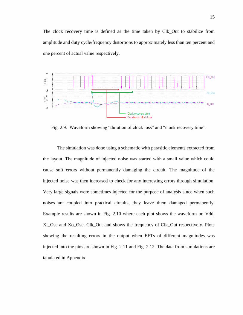
errors. For this circuit, an error may be quantified by the “duration of clock loss” and
“clock recovery time” as illustrated in Fig. 2.9. The duration of clock loss is defined as
the time span during which Clk_Out does not change state within a period of the clock.
15
The clock recovery time is defined as the time taken by Clk_Out to stabilize from
amplitude and duty cycle/frequency distortions to approximately less than ten percent and
one percent of actual value respectively.
Fig. 2.9. Waveform showing “duration of clock loss” and “clock recovery time”.
The simulation was done using a schematic with parasitic elements extracted from
the layout. The magnitude of injected noise was started with a small value which could
cause soft errors without permanently damaging the circuit. The magnitude of the
injected noise was then increased to check for any interesting errors through simulation.
Very large signals were sometimes injected for the purpose of analysis since when such
noises are coupled into practical circuits, they leave them damaged permanently.
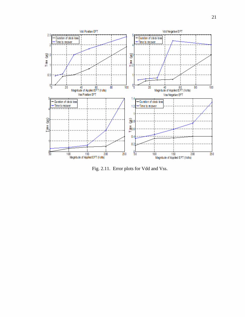
Example results are shown in Fig. 2.10 where each plot shows the waveform on Vdd,
Xi_Osc and Xo_Osc, Clk_Out and shows the frequency of Clk_Out respectively. Plots
showing the resulting errors in the output when EFTs of different magnitudes was
injected into the pins are shown in Fig. 2.11 and Fig. 2.12. The data from simulations are
tabulated in Appendix.

16
(a) Vdd injected with 5 V EFT.
(b) Vdd injected with 30 V EFT.
Fig. 2.10. Simulation results.
Vdd
Xi_Osc
Xo_Osc
Clk_Out
Freq(Clk_Out)
Vdd
Xi_Osc
Xo_Osc
Clk_Out
Freq(Clk_Out)

17
(c) Vdd injected with -30 V EFT.
(d) Vss injected with 150 V EFT.
Fig. 2.10. Simulation results (cont.).
Vdd
Xi_Osc
Xo_Osc
Clk_Out
Freq(Clk_Out)
Vss
Xi_Osc
Xo_Osc
Clk_Out
Freq(Clk_Out)

18
(e) Vss injected with -150 V EFT.
(f) Xi_Osc injected with 150 V EFT.
Fig. 2.10. Simulation results (cont.).
Vss
Xi_Osc
Xo_Osc
Clk_Out
Freq(Clk_Out)
Xi_Osc
Xo_Osc
Clk_Out
Freq(Clk_Out)

19
(g) Xi_Osc injected with -150 V EFT.
(h) Xo_Osc injected with 150 V EFT.
Fig. 2.10. Simulation results (cont.).
Xi_Osc
Xo_Osc
Clk_Out
Freq(Clk_Out)
Xi_Osc
Xo_Osc
Clk_Out
Freq(Clk_Out)

20
(i) Xo_Osc injected with -150 V EFT.
Fig. 2.10. Simulation results (cont.).
Xi_Osc
Xo_Osc
Clk_Out
Freq(Clk_Out)
21
Fig. 2.11. Error plots for Vdd and Vss.

22
Fig. 2.12. Error plots for Xi_Osc and Xo_Osc.
3.5.2. Cause and Mechanism of Failures. The input (Xi_Osc) and output
(Xo_Osc) of the amplifier are compared by a differential buffer to make a decision on the
high or low state of the clock which is then sent to a high gain single-ended inverter to
derive the clock output (Clk_Out). As long as Xi_Osc and Xo_Osc swing around the
same DC value, the differential buffer will detect a change in state. Since the crystal is
required to be driven with low power, the amplitude of oscillation is kept low. In the
event of an EFT, depending up which pin it couples into, one of the oscillating paths is
affected more than the other which disturbs the crossover of oscillations between them
(that is, the DC bias of one signal is changed relative to the other – see Fig. 2.10). The
differential buffer fails to detect the transitions at the point when the voltages on Xi_Osc

23
and Xo_Osc stop crossing over one another even though oscillation are seen at the pins
individually which results in loss of clock.
The simulation results show certain patterns for the noise coupled into the circuit.
The waveforms show that Xo_Osc often shows a greater reaction to noise on Vdd and
Vss than Xi_Osc, for example in Fig. 2.10 (b) and (e). This phenomenon can be
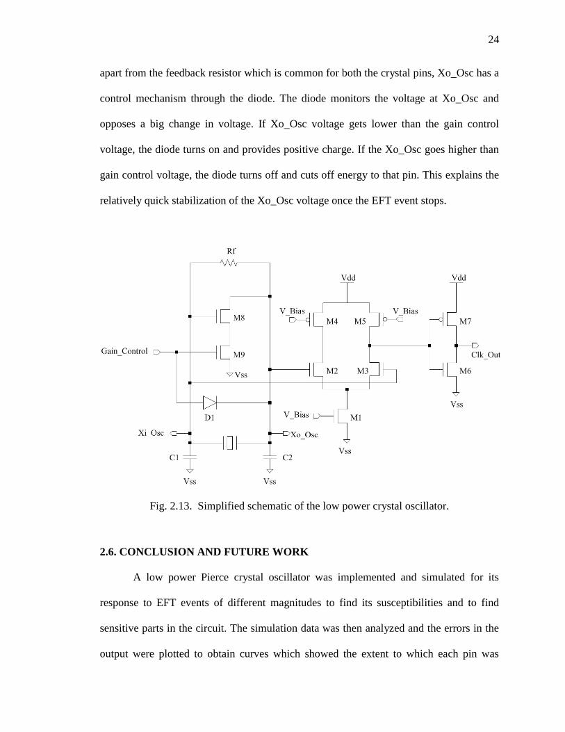
explained using the simplified circuit in Fig. 2.13. The Gain Control net is connected to a
diode apart from the gate of M9 and is the source of energy during low to high phase of
oscillation at Xo_Osc. The diode acts as a feedback path and it is reverse biased when
voltage at Xo_Osc is greater than the Gain Control voltage. When the voltage at Xo_Osc
drops below the gain control voltage plus the turn on voltage of the diode, the diode gets
forward biased and starts pulling up Xo_Osc. This action also reduces the gain of M9
which limits current through M8 thereby weakening the pull-down of Xo_Osc. The gain
control voltage is generated by the low power control circuitry block which is designed
for stability against only minor variations in Vdd or Vss [1]. A big change in Vdd or Vss
impacts the gain control voltage, which is directly reflected on Xo_Osc through the
diode. For noise injections into Vss, the mechanism is slightly different. The EFT couples
through C1 and C2 equivalently but Xi_Osc is connected to the gate of M8 which is seen
as high impedance when compared to the Xo_Osc which is connected to the drain of M8.
The high impedance limits current through C1 and does not allow it to charge when
compared to the current through C2. So the impact of EFT on Xi_Osc disappears with the
EFT whereas the charge in C2 has to be discharged after the EFT event disappears.
The results for EFT injections onto Xi_Osc and Xo_Osc pins reveal that Xi_Osc
is more susceptible for this case compared to the Xo_Osc. The underlying reason is that
24
apart from the feedback resistor which is common for both the crystal pins, Xo_Osc has a
control mechanism through the diode. The diode monitors the voltage at Xo_Osc and
opposes a big change in voltage. If Xo_Osc voltage gets lower than the gain control
voltage, the diode turns on and provides positive charge. If the Xo_Osc goes higher than
gain control voltage, the diode turns off and cuts off energy to that pin. This explains the
relatively quick stabilization of the Xo_Osc voltage once the EFT event stops.
Fig. 2.13. Simplified schematic of the low power crystal oscillator.
2.6. CONCLUSION AND FUTURE WORK
A low power Pierce crystal oscillator was implemented and simulated for its
response to EFT events of different magnitudes to find its susceptibilities and to find
sensitive parts in the circuit. The simulation data was then analyzed and the errors in the
output were plotted to obtain curves which showed the extent to which each pin was

25
susceptible to the noise injections. Based on the results the failure mechanisms were
identified which can be used to improve the circuit design. For instance, the differential
buffer may be modified to track the phase change of the oscillations to better predict a
logic change and make design decisions under moderate noise interference in the circuit.
Another possibility would be to make an intelligent attempt to destroy an IC based on the
study about its susceptibilities. For example, Xi_Osc was found to be the most vulnerable
pin in the IC which may be targeted specifically to destroy its function. The knowledge of
the circuit gained can also be used to create a universal model for Pierce crystal
oscillators that can be used to predict failures to certain extent. The model for failure is
not implemented in this work but may be done in future so that failures can be predicted
without destroying the actual circuit or hardware.
26
3. IMPACT OF A CML–BASED CLOCK DISTRIBUTION NETWORK ON IC
EMISSIONS
3.1. INTRODUCTION
Synchronous digital circuits use clock signals to obtain synchronous operation of
their functional blocks and components. The clock is one of the fastest signals in an
integrated circuit. Typically the clock is routed in the form of a tree branching out to
different digital circuitry in such a way that the path from the root to the leaves have the
same delay. Buffers are used along the paths to minimize rise- and fall-times. Depending
upon the design complexity, the number of buffers may range from a few hundred to
several millions. Designers may use either single ended or differential buffers. There are
many tradeoffs in terms of speed, power consumption, etc between them. In general the
single ended design offers simplicity, low power consumption, and low jitter whereas the
differential design can operate with better immunity to noise but at the expense of design
area and power consumption [7].
In a traditional single ended clock distribution networks, the buffers produce
switching noise every time the clock undergoes a transition. This switching activity
results in electromagnetic emissions which could couple to other circuits inside the IC or
to other nearby ICs and interfere with their operation. This coupling can be particularly
important in mixed signal design since analog circuits are very sensitive to noise. In the
case of an IC, the dimensions are small enough that it cannot radiate efficiently by itself
for frequencies below a few GHz, though at lower frequencies the clock tree causes noise
on the power distribution network of the PCB which may cause radiation through the
larger structures at the PCB level or the time varying switching currents on the lead frame

27
of the IC may cause fields which could couple to nearby structures that act as efficient
antennas, thus allowing the clock tree to cause a radiated emissions problem.
The use of differential clocks could reduce EMI but this increases static power
dissipation which may not be desirable in certain designs. There is no rule of thumb for
making a choice between single ended and differential clock distribution networks. It is
important to understand the tradeoffs involved and decide the parameters based on the
design objective of a circuit. The following chapter presents a preliminary study of the
use of the relative advantage of current mode logic (CML) compared with single-ended
logic within a clock tree. Comparisons are made for a single configuration, based on
power consumption, rise and fall times, noise generated during transitions, and jitter.
3.2. BACKGROUND
3.2.1. Clock Distribution. A clock edge should reach every circuit in an IC at the
same instant. A number of factors like propagation delay and skew due to interconnect
and variable loads can throw the clock out of synchronization. In order to handle these
uncertainties, a clock distribution network (CDN) relies on clock buffers for gain and
signal propagation. The clock buffers are placed at specific locations to regulate the time
of arrival of the clock at the destinations. There are numerous techniques to design a
CDN. One of the simplest and most common structures of the CDN is the H-tree CDN
(Fig. 3.1). Each clock buffer drives four more buffers which are placed equidistant from
the previous stage in an effort to make the propagation delay and associated losses and
capacitances equal. In this study the H-tree is used to compare the impact of CMOS

28
buffers and CML buffers on EMI in the following sections. A detailed description about
clock trees is found in [14].
Fig. 3.1. H-Tree Scheme for CDN.
3.2.2. Differential Buffers. The differential amplifier, known for its properties
like low level signaling and common mode noise rejection, is a common choice in many
high speed and high performance analog and mixed signal designs. A detailed analysis
and design of CMOS differential amplifier is discussed in [10]. A clock buffer is
essentially a high gain amplifier. When differential buffers are implemented in a design
for propagating a signal for a relatively long distance, apart from the benefits of
preserving the signal from line losses, they also offer high immunity from noise
interference which can improve the signal integrity [12]. This is one of the reasons why
circuit designers choose differential signaling when it comes to creating a robust design.

29
3.2.3. Current Mode Logic. Current mode logic (CML) is commonly used in
high speed CMOS digital design. CML is based on a differential architecture and can
work at high speeds compared to single ended logic [3]. CML also offers low power
operation and common mode noise immunity [7], [8]. For this reason, CML is commonly
used as buffers for high speed inter die communications. Current mode logic realizes
logic values by steering current between two branches. The basic building blocks of
current mode logic are shown in Fig. 3.2. It consists of a DC current source, pull-up
resistors and a logic block connected in between to implement some logic function.
Fig. 3.2. Basic blocks of a CML.
Fig. 3.3 shows a classic CML inverter circuit. Transistor M1 is always under
saturation and acts as a constant current source. The size and biasing of M1 determines
the maximum current that can flow through the transistors M2 and M3. M2 and M3 work

30
in either saturation or in the triode region depending upon the inputs Vin1 and Vin2. The
load resistors determine the output voltage swing, ∆V = I × R. CML is typically designed
for a 400 mV swing.
Fig. 3.3. CML inverter.
3.2.4. Advantages. A CML buffer can work at higher frequencies than its single
ended counterpart. CML does not depend on a PMOS transistor for a logic transition
which can otherwise limit the bandwidth [1]. In some processes, which require an all
CMOS implementation or where space is an issue, the resistors are replaced by active
PMOS loads. This has some impact on the speed of operation [9] due to lower bandwidth
of the PMOS transistor.
A big advantage of the CML is that it can minimize switching noise. Ideally CML
consumes a constant current and does not induce switching noise in the power
distribution lines when there is transition in the logic, unlike its single ended CMOS

31
counterpart. This is an important property which enables circuits designed using CML to
be placed near sensitive circuits without interfering with them. Data security and
cryptography ICs sometimes make use of this property to prevent differential power
analysis attacks [11]. A major downside to CML, however, is that it consumes static
power even when there are no transitions. This could possibly limit its application in
certain designs where power consumption is a concern. Portable devices like cell phones
and tablet PCs have strict power limitations. With increasing device densities, channeling
out generated heat also becomes critical.
3.2.5. CML Buffer Designs. One common usage of CML involves I/O designs
where high speed buffers at the rate of tens of Gbps are desired. These buffers require a
high driving strength since the signals are meant to be transmitted off chip to other
devices. High driving strength with fast rise/fall times can be achieved by tapering a
chain of CML buffers as shown in Fig. 3.4 [5].Buffer designs for I/O typically have a
resistor as a pull up to allow good matching with off chip transmission lines. The resistor
is generally small and can be implemented as drain resistance without much cost in area.
The static power dissipation is justified because off chip signal transmissions need more
power than driving a signal through the core interconnections of an IC and high-speed
buffers typically work in a switching state.

32
Fig. 3.4. A CML output buffer driving off-chip loads (Figure from Ref [5]).
The CML output buffer is driven by a series of tapered CML buffer stages to
build up enough drive strength to drive off-chip loads. In this case the load is a
transmission line with an appropriate termination. This work uses a capacitor, CDN, for
neutralizing the input-output coupling due to the device overlap capacitance [5].
For the core logic circuitry in the IC, an all CMOS design approach is preferred
which is accomplished by using active PMOS loads. High resistances in the order of kilo-
ohms are simple and area efficient when active loads are used. However active loads
using PMOSFETs may not be as efficient as a resistor at higher frequencies and can
suffer from amplitude attenuation. Fig. 3.5 shows the simulation results for the output of
each buffer when four buffers are connected in series and a 100ps pulse was applied as
input to the first buffer. In Fig. 3.5(b) the outputs of the buffers was implemented with
resistors as pull-up and do not show significant amplitude attenuation as compared to the
outputs of buffers with active load as shown in Fig. 3.5(c). The amplitude of the outputs
from consecutive buffers using active loads is attenuated and has increased slopes
compared to the buffers with resistive load. The performance of a PMOSFET can be

33
improved using techniques like inductive peaking and multiple supply voltages for thick
gate oxide transistors as discussed in [9], but this requires additional components and
design complexity.
(a) Schematic showing the connections between buffers.
(b) Pulse responses for CML buffer with “non-salicided resistor” as load.
Fig. 3.5. Illustration for amplitude attenuation (Figure from Ref [9]).
1 2
3

34
(c) Pulse responses for CML buffer with active PMOS transistor as load.
Fig. 3.5. Illustration for amplitude attenuation (Figure from Ref [9]), (cont.).
Ideally, the dynamic power generated by a CML gate is nearly zero, since the
current drawn by a CML gate is constant. The static power dissipation, however, is
relatively high. This power is due to the current, ISS from the constant current source
which is present even when there are zero transitions in the logic. In other words, the
static power dissipation will exist as long as the circuit is powered ON. A number of
techniques have been suggested to reduce the static power consumption, for example as
discussed in [6], [7]. These techniques, like putting the circuit to sleep when not in use,
are also commonly used in single-ended clock tree design.
Though CML has high static power dissipation, the total power consumed
remains constant with frequency. For single-ended CMOS logic, the dynamic power
consumption increases at high frequencies and can be larger than the total power
consumed by a CML gate for the same frequency, as shown in Fig. 3.6 [4]. The point
1
2
3

35
where the power consumption of CML is lower than single-ended logic depends on the
design and its dynamic power consumption.
Fig. 3.6. Power consumption as a function of frequency (Figure from Ref [4]).
While it has been clearly shown in the literatures that speed and power are the
main trade-offs for CML [7], the relation between power and emission lacks some
understanding. An analysis for performance of a CML logic gate under harsh
electromagnetic environments has been presented in [2]. The impact of CML on
emissions and performance in a clock distribution network has not been thoroughly
studied in the existing literature, which is the motivation for the following study.
3.3. DESIGN OF CML BUFFER FOR CLOCK DISTRIBUTION NETWORK
3.3.1. Design Objective. The design objective is to build a simple clock
distribution network using CML with comparable timing/jitter performance to a single-

36
ended CMOS logic design, and then to compare the two structures based on their
potential to generate electromagnetic emissions. The requirements for a clock buffer in a
clock distribution network are different from that of an I/O buffer. In the following
sections, a simple methodology is presented to create CML clock buffers.
3.3.2. CML Buffer Design. An all MOSFET implementation of a CML buffer is
shown in Fig. 3.7. The pull-up resistors are implemented by active PMOS FETs. In order
to make an efficient logic transition without wasting power, the entire tail current should
be steered to one of the branches towards the end of a transition. For this to happen, the
transistors M1, M2 and M3 should always be in saturation or cut-off. Say for example,
VIN,1 goes low and VIN, 2 goes high. M1 should always be in saturation since it has to be a
constant current source. M2 should be turned OFF and M3 should be in saturation so that
the tail current ISS flows through M5, M3 and M1. This results in VOUT, 1 to go high (=
VDD) and VOUT, 2 to go low (= VDD - ∆V).
Fig. 3.7. CML inverter with active load.

37
Based on the above requirements, the CML buffer design equations can be
formulated as follows.
Conditions for M1 to be in saturation,
VG1 = VGS1 = Vbias> VT, n (1)
VGD1< VT, n for M1 to be saturation. (2)
VD1> (Vbias – VT, n) (3)
From (1) and (2),
VT, n<Vbias< VDD
Conditions for M3 to be in saturation (when VIN, 2 = VDD),
VGS3 = VG3 – VS3 = VDD – VD1< VT. n; (4)
Since,
VG3 = VDD
VGD3 = VG3 – VD3
VGD3 = VDD – (VDD – IM3.RM5)
VGD3 = IM3.RM5< VT, n (5)
Conditions for M2 to be OFF when M3 is in saturation (VIN, 1 = low; VIN, 2 = high). Since,
VG2 = VDD – ∆V; VD2 = VDD; VS2 = VD1,
VGD2 = VG2 – VD2 = |∆V| < VT, n (6)

38
and,
VGS2 = VG2 – VS2 = VDD - ∆V – VD1< VT, n (7)
Equations (4) and (5) imply that the voltage drop ∆V (=IM3.RM5 = IM2.RM4) cannot
be higher than the threshold voltage of an NFET, which depends on the process being
used. This condition should not have any serious implications on the feasibility of the
design due to noise margin requirements, since the threshold voltage scales down at a
slower rate than the supply voltage with advances in technology.
3.3.3. Drive Capability. The capacitances associated with one CML buffer
driving another has been discussed in [5]. Capacitance is directly related to the size of the
transistors and interconnects. For this preliminary study, the impact of interconnect will
be ignored. Generally in a CDN, all the buffers are identical and each buffer drives four
buffers which are optimized for equal propagation delay and skew. The driving buffer
sees four times its own input capacitance as a load (Fig. 3.8). The effective load
capacitance is given by
CL = CP + 4*CG + CLine (8)
where CP represents the equivalent capacitances seen at output node of the driver, CG is
the gate capacitances at the input to the next stage and CLine is the parasitic capacitances
due to the trace or interconnects, which is approximated here as CLine=0. The operation
during high state and low state output for a single branch is not exactly symmetric. This
is due to the different capacitances seen during high and low states in each branch of a

39
CML stage and to differences between the driving PFET and NFET. When the output
goes high only the parasitic capacitances due to the active load M4 or M5 shows an effect
on the slope of output. But when the output has to go low, the current has to charge the
additional parasitic capacitance seen in M2 or M3 and M1.
Input gate
capacitances
CG
Equivalent parasitic
capacitances
CP
Fig. 3.8. Load seen by a CML clock buffer in a CDN.
3.3.4. Proposed Design. Based on the above discussion, a CML clock buffer was
designed to have low current or power consumption. This objective was mainly achieved
by fixing two design goals. One was to minimize the effective load capacitance by
optimizing the sizing of the transistors so that the transitions can be faster, smoother and
also consume less current. The other was to maintain the swing level in this process for
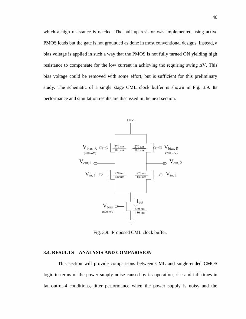
40
which a high resistance is needed. The pull up resistor was implemented using active
PMOS loads but the gate is not grounded as done in most conventional designs. Instead, a
bias voltage is applied in such a way that the PMOS is not fully turned ON yielding high
resistance to compensate for the low current in achieving the requiring swing ∆V. This
bias voltage could be removed with some effort, but is sufficient for this preliminary
study. The schematic of a single stage CML clock buffer is shown in Fig. 3.9. Its
performance and simulation results are discussed in the next section.
Fig. 3.9. Proposed CML clock buffer.
3.4. RESULTS – ANALYSIS AND COMPARISION
This section will provide comparisons between CML and single-ended CMOS
logic in terms of the power supply noise caused by its operation, rise and fall times in
fan-out-of-4 conditions, jitter performance when the power supply is noisy and the

41
overall impact on emissions. All the simulations are performed in Spectre, a tool part of
Cadence Virtuoso 6.1.3, using TSMC 180 nm deep technology. The waveforms are then
plotted in Matlab R2011a. All the simulation results are obtained for a frequency of 1
GHz unless otherwise specified.
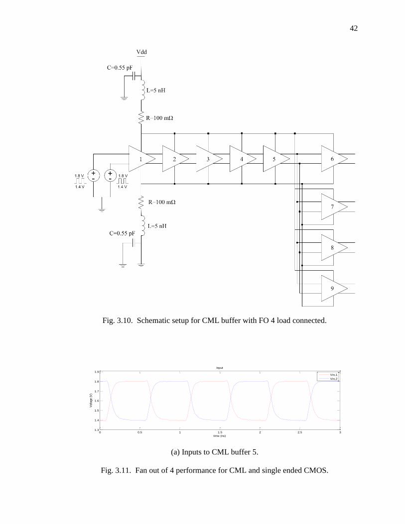
3.4.1. Single Stage with a fan-out of 4. First, the designed clock buffer was
tested for its performance in a single stage H-tree, which is essentially one buffer driving
four other buffers connected as fan-out-of-4 loads. The results will be compared with an
equivalent circuit built in single-ended CMOS logic. The CML test schematic and
resultant waveforms for both the CML and single-ended buffers are shown in Fig. 3.10
and Fig. 3.11, respectively. The simulation uses ideal pulse waveform generator inputs at
the first buffer with ideal rise and fall times. A series of buffers are used before the circuit
under test in order to create a more realistic input signal.
Table 3.1 shows the rise and fall time for the 5th
buffer in the buffer chain (which
drives the fan-out-of-4 load) for the CML clock buffer and the minimum sized single-
ended CMOS buffer. Since the CML buffer was designed for low power consumption, it
only has a pull-down current of ISS = 23 µA, which is too small to charge the parasitic
capacitances quick enough to have a fast fall time. For the single-ended CMOS buffer,
the rising edge is not as fast as the falling edge due to the lower mobility of carriers in the
pull-up PFET used.
42
Fig. 3.10. Schematic setup for CML buffer with FO 4 load connected.
(a) Inputs to CML buffer 5.
Fig. 3.11. Fan out of 4 performance for CML and single ended CMOS.
0 0.5 1 1.5 2 2.5 31.3
1.4
1.5
1.6
1.7
1.8
1.9
time (ns)
Volta
ge (
V)
Input
Vin,1
Vin,2

43
(b) Outputs 5 of CML buffer 5.
(c) Input to single-ended CMOS buffer 5.
(d) Output of single-ended CMOS buffer 5.
Fig. 3.11. Fan out of 4 performance for CML and single ended CMOS (cont.).
Table 3.1. Performance for FO 4 loads
CMOS CML
Input Output Input Output
Rise Time 50 ps 148 ps 84 ps 152 ps
Fall Time 37 ps 97 ps 103 ps 230 ps
0 0.5 1 1.5 2 2.5 31.3
1.4
1.5
1.6
1.7
1.8
1.9
time (ns)
Vol
tage
(V
)
Output
Vout,1
Vout,2
0 0.5 1 1.5 2 2.5 3-0.5
0
0.5
1
1.5
2
time (ns)
Voltage (
v)
Input
0 0.5 1 1.5 2 2.5 3-0.5
0
0.5
1
1.5
2
time (ns)
Voltage (
v)
Output

44
3.4.2. Jitter Performance. The previous result on Table 3.1 showed that the rise
and fall times for CML gate used here is higher than the single-ended CMOS logic.
Experiments were performed to try to reduce the rise and fall times of the CML logic
gate, but it was not reasonable to reduce them to the same level as the single-ended logic.
The most important reason for fast rise-and-fall times is to minimize the impact of power
supply noise on jitter. The CML gate should naturally be more resistant to power supply
noise than the single-ended gate [7], so the rise- and fall-time is less important. If the two
designs have similar jitter performance in the presence of noise, then it is reasonable to
compare the emissions between the two circuits.
For this test setup, a chain of buffers were considered of which two stages are
exposed to power supply noises (Fig. 3.12). In general different design strategies have
their own strict upper limits for noises which are generated by the operation of their
circuits. Since the testing conditions should be realistic, the power supply noise should
occur at every instant and the noise voltage level should be less than 10% of the power
supply voltage which is a standard design goal. A power supply voltage noise of +/- 160
mV was created in simulation by using single ended inverters made up of big FETs
driving a capacitive load, switching at a frequency a little higher than the clock frequency
so that the noise can occur at every instant with a period of the clock when the simulation
is run for a large number of cycles. The noise generator was connected to power supply
line for buffers 5 and 6 which was isolated from the power lines feeding the other stages.
The big FETs are an approximation to transistors in an IC which creates switching noise.
The output of this stage is then connected to a couple of normal stages and the output of
the last stage, numbered 8 was monitored.

45
The simulation setup is shown in Fig. 3.12 and the jitter in the output clock in Fig.
3.13. The measured jitter for about 200 cycles of the clock is shown in Table 3.2. While
the CML and single-ended buffers used here did not have the same jitter performance,
they were comparable, indicating that the noise generated by these CML and single-
ended clock trees could reasonably be compared to one another as “equivalent” clock
trees for this preliminary study.
(a) CML.
Fig. 3.12. Schematic setup for analyzing immunity under noisy power supply lines.

46
(b) Single ended CMOS.
Fig. 3.12. Schematic setup for analyzing immunity under noisy power supply lines
(cont.).
(a) CML.
Fig. 3.13. Jitter in the output clock under noisy power supply lines.
47
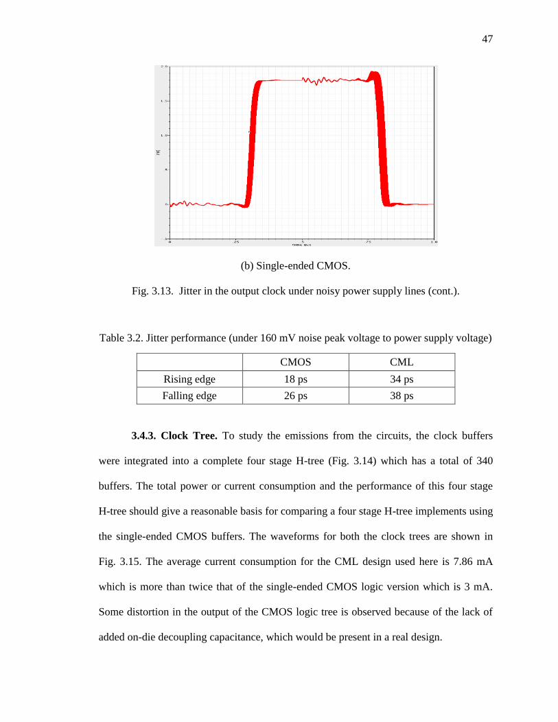
(b) Single-ended CMOS.
Fig. 3.13. Jitter in the output clock under noisy power supply lines (cont.).
Table 3.2. Jitter performance (under 160 mV noise peak voltage to power supply voltage)
CMOS CML
Rising edge 18 ps 34 ps
Falling edge 26 ps 38 ps
3.4.3. Clock Tree. To study the emissions from the circuits, the clock buffers
were integrated into a complete four stage H-tree (Fig. 3.14) which has a total of 340
buffers. The total power or current consumption and the performance of this four stage
H-tree should give a reasonable basis for comparing a four stage H-tree implements using
the single-ended CMOS buffers. The waveforms for both the clock trees are shown in
Fig. 3.15. The average current consumption for the CML design used here is 7.86 mA
which is more than twice that of the single-ended CMOS logic version which is 3 mA.
Some distortion in the output of the CMOS logic tree is observed because of the lack of
added on-die decoupling capacitance, which would be present in a real design.

48
Fig. 3.15 and Fig. 3.16 show the time-domain waveform and frequency-domain
spectrum for the total power supply current consumed by the CML and single-ended
CMOS version of the four stages H-tree. The time-domain waveform shows significantly
less fluctuation for the CML tree than the CMOS clock tree, indicating it will have far
lower high-frequency emissions. Comparison of the current consumed by the two trees
implemented here shows the current to be more than 100 dB lower for the CML tree at
harmonics of 1 GHz, the input clock frequency. The even harmonics are much larger than
the odd harmonics, since switching occurs on both the rising and falling edge of the
clock.
Fig. 3.14. Schematic of 4 stage H-tree CDN.

49
(a) Output of last stage for CML clock tree.
(b) Total current consumed by the tree for CML clock tree.
(c) Output of last stage for single-ended CMOS clock tree.
(d) Total current consumed by the tree for single-ended CMOS clock tree.
Fig. 3.15. Input and output waveform for 4 stage H-tree CDN.
0 0.5 1 1.5 2 2.5 31.3
1.4
1.5
1.6
1.7
1.8
1.9
time (ns)
Vol
tage
(V
)
Output
0 0.5 1 1.5 2 2.5 37.78
7.8
7.82
7.84
7.86
7.88
7.9
7.92
time (ns)
Curr
ent
(mA
)
Current drawn form power supply
0 0.5 1 1.5 2 2.5 3-0.5
0
0.5
1
1.5
2
2.5
time (ns)
Voltage (
V)
Output
0 0.5 1 1.5 2 2.5 3-5
0
5
10
15
time (ns)
Curr
ent
(mA
)
Current drawn form power supply

50
(a) CML power supply current spectrum
(b) single-ended CMOS power supply current spectrum
Fig. 3.16. Spectrum of the total current consumed by the CML and single-ended CMOS
4 stage H-tree.
0 1 2 3 4 5 6 7 8 9
-350
-300
-250
-200
-150
-100
-50
0
X: -0.004999
Y: -96.9
Frequency (GHz)
Curr
ent
(dB
)
Current Spectrum for CML
X: 1.995
Y: -232.5
0 1 2 3 4 5 6 7 8 9
-260
-240
-220
-200
-180
-160
-140
-120
-100
-80X: -0.005
Y: -107.6
Frequency (GHz)
Curr
ent
(dB
)
Current Spectrum for single ended CMOS
X: 1.995
Y: -123.9

51
3.5. CONCLUSION AND FUTURE WORK
A simple CDN using four stages H-tree and CML clock buffers designed for low
static power consumption was compared to an equivalent CDN designed using single-
ended CMOS logic. Though the rise and fall times of the CML design were high, the
jitter performance was comparable to the single-ended design, allowing reasonable
comparison between the high-frequency noise generated by the two designs. For a four
stage H-tree, the CML design 100 dB less dynamic power supply current noise at
harmonics of the clock frequency than the single-ended design. While this level of
reduction is not expected in practice, and many additional variables should be studied,
this result illustrates that CML has the potential to significantly reduce emissions from
the clock. Further study should be performed to confirm this result, using a more
complete model of the power delivery network and circuit parasitics and more carefully
tuning parameters between the CML and single-ended design to generate a completely
fair comparison.

52
4. CONCLUSION
A low power Pierce crystal oscillator was tested with EFT injections through
simulations and the resultant data was analyzed to find the cause and failure mechanisms.
One of the main causes of failure was found to be unequal noise coupling to the crystal
pins due to the feedback control present on only one pin.
A simple initial investigation on the potential to reduce emissions from the IC was
performed based on current mode logic (CML).The emissions from a CML-based clock
distribution network (CDN), was demonstrated to have much lower emissions without
significantly greater power consumption but at a cost of roughly double the area than a
clock tree based on single-ended CMOS logic. The analyses had many assumptions
which may be difficult to achieve in practical designs. A more detailed study is needed
that includes a more realistic simulation model in order to make a better comparison
between CML and single ended CMOS design.

53
APPENDIX
The simulation data and results for EFT injection into various pins of the Pierce
crystal oscillator are tabulated in Table A.1.
Table A.1. Numerical data from simulation results
Vdd injected with positive EFT
Applied EFT
Peak positive
voltage seen at
VDD
Duration of loss in
clock output Time to recover
5 V 5.57 V None 450n s
15 V 6.6 V 425n s 550n s
30 V 8.6 V 500n s 1.5u s
50 V 10.2 V 800n s 1.8u s
100 V 15 V 1.9u s 2.4u s
Vdd injected with negative EFT
Applied EFT
Peak negative
voltage seen at
VDD
Duration of loss in
clock output Time to recover
-5 V 4.2 V None 500n s
-15 V 2.45 V 400n s 600n s
-30 V -0.27 V 500n s 700n s
-50 V -1.3 V 550n s 4.4u s
-100 V -7.3 V 3u s 4u s

54
Vss injected with positive EFT
Applied EFT
Peak positive
voltage seen at Vss
pin
Duration of loss in
clock output Time to recover
50 V 1 V None 300n s
100 V 1.9 V 300n s 400n s
150 V 3 V 440n s 600n s
200 V 4 V 500n s 2u s
250 V 4.9 V 1.42u s 5u s
Vss injected with negative EFT
Applied EFT
Peak negative
voltage seen at Vss
pin
Duration of loss in
clock output Time to recover
-50 V -0.98 V 160n s 350n s
-100 V -1.9 V 350n s 450n s
-150 V -2.8 V 360n s 590n s
-200 V -3.7 V 400n s 750n s
-250 V -4.8 V 400n s 1.3u s

55
Xi_Osc injected with positive EFT
Applied EFT
Peak positive
voltage seen at
Xi_Pin
Duration of loss in
clock output Time to recover
50 V 4 V 360n s 450n s
100 V 5.77 V 450n s 550n s
150 V 6.2 V 550n s 600n s
200 V 6.4 V 550n s 600n s
250 V 6.77 V 560n s 750n s
Xi_Osc injected with negative EFT
Applied EFT
Peak negative
voltage seen at
Xi_Pin
Duration of loss in
clock output Time to recover
-50 V -746m V 450n s 550n s
-100 V -922m V 640n s 740n s
-150 V -1.2 V 790n s 890n s
-200 V -1.45 V 790n s 890n s
-250 V -1.6 V 840n s 950n s

56
Xo_Osc injected with positive EFT
Applied EFT
Peak positive
voltage seen at
Xo_Pin
Duration of loss in
clock output Time to recover
50 V 3.92 V None 350n s
100 V 5.77 V None 450n s
150 V 6.1 V 250n s 450n s
200 V 6.3 V 280n s 450n s
250 V 6.43 V 360n s 450n s
Xo_Osc injected with negative EFT
Applied EFT
Peak negative
voltage seen at
Xo_Pin
Duration of loss in
clock output Time to recover
-50 V -596m V None 420n s
-100 V -992m V None 520n s
-150 V -1 V 260n s 500n s
-200 V -1.45 260n s 500n s
-250 V -1.8 V 410n s 510n s

57
BIBLIOGRAPHY
[1] Shahab Ardalan; Kambiz K. Moez; Manoj Sachdev; Mohamed I. Elmasry,
“Distributed Current Mode Logic,” IEEE North-East Workshop on Circuits and
Systems, pp.229-232, June 2006.
[2] Siliang Hua; Qi Wang; Hao Yan; Donghui Wang; Chaohuan Hou , “A high speed
low power interface for inter-die communication,” 10th IEEE Internationa l
Conference on Solid-State and Integrated Circuit Technology (ICSICT), pp.1916-
1918, 1-4 Nov. 2010.
[3] Green, M.M.; Singh, U., “Design of CMOS CML circuits for high-speed
broadband communications,” ISCAS '03. Proceedings of the 2003 International
Symposium on Circuits and Systems, vol.2, pp. II-204- II-207 vol.2, 25-28 May
2003.
[4] Sumathi, M., “Performance and analysis of CML Logic gates and
latches,” International Symposium on Microwave, Antenna, Propagation and
EMC Technologies for Wireless Communications, pp.1428-1432, 16-17 Aug.
2007.
[5] Heydari, P., “Design and analysis of low-voltage current-mode logic
buffers,” Fourth International Symposium on Quality Electronic Design, pp. 293-
298, 24-26 March 2003.
[6] Anis, M.H.; Elmasry, M.I., “Self-timed MOS current mode logic for digital
applications,” ISCAS 2002. IEEE International Symposium on Circuits and
Systems, vol.5, pp. V-113- V-116 vol.5, 2002.
[7] Badel, S.; Leblebici, Y., “Breaking the Power-Delay Tradeoff: Design of Low-
Power High-Speed MOS Current-Mode Logic Circuits Operating with Reduced
Supply Voltage,” ISCAS 2007. IEEE International Symposium on Circuits and
Systems, pp.1871-1874, 27-30 May 2007.
[8] Y. Liu, J. Quan, H. Yang, and H. Wang, “MOS current mode logic circuits:
design consideration in high-speed low-power applications and its future trend, a
tutorial,” International J. High Speed Electronics and Systems, vol. 15, no. 3, pp.
599–614, Sep. 2005.
[9] Kalantari, N.; Green, M.M., “All-CMOS High-Speed CML Gates with Active
Shunt-Peaking,” ISCAS 2007. IEEE International Symposium on Circuits and
Systems, pp.2554-2557, 27-30 May 2007.
[10] B. Razavi, “Design of Analog CMOS Integrated Circuits,” New York: McGraw-
Hill, 2001, pp. 101–134.

58
[11] Toprak, Z.; Leblebici, Y., “Low-power current mode logic for improved DPA-
resistance in embedded systems,” ISCAS 2005. IEEE International Symposium
on Circuits and Systems, pp. 1059- 1062 Vol. 2, 23-26 May 2005.
[12] Hatirnaz, I.; Leblebici, Y., “Twisted differential on-chip interconnect architecture
for inductive/capacitive crosstalk noise cancellation,” International Symposium
on System-on-Chip, pp. 93- 96, 19-21 Nov. 2003. asfasfdassdaadasdasd
[13] S. B. Dhia, M. Ramdani, and E. Sicard, “Electromagnetic Compatibility of
Integrated Circuits - Techniques for Low Emission and Susceptibility,” New
York: Springer-Verlag, 2006. sfdgdfgsdfklgjsdfgjksdfgjsdfklgjskldfgjsdfkgjfasdf
[14] T. Xanthopoulos, “Clocking in Modern VLSI Systems,” Springer Publishing
Company, Incorporated, 2009, ch. 2.sdgsdgsdgsdgsdfgsdgdsfgsdfgdfgsdgsgdfgsd
[15] P. E. Gronowski, W. J. Bowhill, R. P. Preston, M. K. Gowan, and R. L. Allmon,
“High-performance microprocessor design,” IEEE J. Solid-State Circuits, vol. 33,
pp. 676–686, May 1998.
[16] Yao, S.; Zhu, H.; Wu, X., “Design of Low Power CMOS Crystal Oscillator with
Tuning Capacitors,” Engineering Letters, vol.14, Issue.1, pp.40-44, 2007.
[17] Vittoz, E.A.; Degrauwe, M.G.R.; Bitz, S., “High-performance crystal oscillator
circuits: theory and application,” IEEE Journal of Solid-State Circuits, vol.23,
no.3, pp.774-783, Jun 1988.
[18] Jayong Koo; Lijun Han; Herrin, S.; Moseley, R.; Carlton, R.; Beetner, D.G.;
Pommerenke, D., “A Nonlinear Microcontroller Power Distribution Network
Model for the Characterization of Immunity to Electrical Fast Transients,”
Electromagnetic Compatibility, IEEE Transactions on , vol.51, no.3, pp.611-619,
Aug. 2009

59
VITA
Vijay Kanagachalam was born in Tamil Nadu, India. Vijay completed his school
education in St. Paul’s Matriculation Higher Secondary School, Neyveli, India. He
received his Bachelor’s degree in Electronics and Communications from Sri
Sivasubramaniya Nadar College of Engineering (Anna University), Chennai, India in
July 2010. He joined Missouri University of Science and Technology (formerly
University of Missouri – Rolla) in Fall 2010 and received his Master’s degree in
Electrical Engineering in December 2012. His areas of interests include VLSI, EMC,
Signal Integrity and Digital Designs.