Embed Size (px)
Citation preview
1
Electromagnetic Interference and Digital Circuits: An Initial Study of Clock Networks
Hongxia Wang, Samuel V. Rodriguez, Cagdas Dirikand Bruce Jacob
Department of Electrical and Computer EngineeringUniversity of Maryland, College Park, MD 20742
{hwang, samvr, cdirik, blj}@eng.umd.edu
http://www.ece.umd.edu/~blj/integrity/
ABSTRACT
Radio Frequency Interference (RFI) can have adverse effects on commercial electronics. Current properties of
high performance integrated circuits (IC’s), such as very small feature sizes, high clock frequencies, and
reduced voltage levels, increase the susceptibility of these circuits to RFI, causing them to be more prone to
smaller RFI levels. Besides, recent developments of mobile devices and wireless networks create a hostile
electromagnetic environment for IC’s. Therefore, it is important to generalize the susceptibility of IC’s to RFI.
In this study, we investigate the susceptibility levels and frequency ranges of RFI to the clock network of a
digital device, an 8-bit ripple counter, designed and fabricated using AMI 0.5
µ
m process technology. Our
experimental setup is designed to couple a pulse modulated RF signal using the direct pin injection method.
Our experiments show that relatively low levels of RFI (e.g., 16.8 dBm delivered RF peak power with carrier
frequency of 1 GHz) could adversely affect the normal functioning of the device under test. In the end, SPICE
simulations show the sensitivity of a flip-flop, the basic building block of clock network, which further explains
the experimental results.
Keywords:
RFI, Pin direct injection method, Power reflection coefficient, Pulsed modulated RF, Clock
network, metastability
1 INTRODUCTION
Numerous other structures in a computer system (e.g., external wires, cables, PCB traces, bonding
interconnects, chip pins like power, ground, and data lines), can act as antennae in the presence of RFI, which
is either radiated from powerful radio transmitters, wireless network devices, mobile phones and PDAs, or
intentionally generated for malicious reasons. These unintentional antennae can serve to couple RF noise into
the core circuit [1][2][3]. RFI that is coupled by the system can induce unwanted currents, which cause various
disturbances. Also, current high performance integrated circuits (IC’s), such as microprocessors, have very
2
small feature sizes and are clocked at frequencies well into the GHz range while operating at reduced voltage
levels. Although this has improved the ability and performance of modern systems, it has also increased their
susceptibility to RFI. The electrical charge required in transistor switching decreases with relatively smaller IC
feature sizes. Correspondingly, the energy required to make the device to switch is reduced, making it easier to
disturb the circuit with lower RFI signal levels. As the switching speed of the IC’s increases and the supply
voltage scales down, the noise margin also becomes smaller. This allows external disturbances to degrade the
signal integrity more easily. Even though with the advanced circuit design technology, additional circuitry
design methodologies, such as offset the switching voltage, using schmidt triggering devices or bus hold
circuitry, increasing the signal to noise radio, and adding input/output buffers to the circuit, could be applied to
improve the noise immunity, these techniques are not generally used in the simple digital circuit systems.
Besides RF noise coupling, the inherent non-linear behavior of electronic devices in digital circuits
can also cause RF signal rectification and amplification and is said to be the primary upset mechanism for
integrated circuits under RFI [4]. Also, inter-modulation, cross-modulation and other disturbances are
immediate effects of interference [8]. These unwanted interferences, when interpreted as or superimposed on
system signals, can cause spurious state changes on logic devices and system-level breakdown [3][4].
The power levels and frequency range for which circuits are susceptible to RFI have been studied
recently. Previous studies observed changes on the I-V characteristics of diodes, BJTs, and MOSFETs under
RFI [1]. Susceptibility levels of a microcontroller and a DSP chip have been measured for RF interference up
to 400 MHz, and data corruption was observed on the communication path between the microcontroller and
RAM memory [2]. The study also showed that 20 dBm RFI at 350 MHz was enough to trigger the reset pin of
a voltage regulator. Another study investigated the effects of RFI on the input ports of a 0.7 µm CMOS inverter
with frequency range between 20 MHz and1 GHz and power levels up to 15 dBm [3]. Dynamic failures in the
form of variations in input pad propagation delay and static failures were observed when pad output signals
were misinterpreted as they strayed beyond the high and low voltage logic thresholds. With devices running at
higher frequencies, there is a growing concern over the electromagnetic compatibility of IC’s in hostile RFI
environments in wider frequency ranges, such as at and above 1 GHz. To this end, power levels and frequency
ranges of RFI to which a typical synchronous high speed IC’s are more sensitive, have been studied in this
paper.
3
2 BACKGROUND - DIGITAL CIRCUITS AND THEIR VULNERABILITIES
This work follows a system-level approach to quantify and generalize the susceptibility levels of
simple digital IC’s. On the system-level, signals in the basic building blocks of memory and CPU are mainly
composed of the clock, power/ground, and data networks. These signals are interpreted differently under
normal operation. The timing and voltage levels of the data input/output signals are important, whereas for
clock signals, if it is going to drive all the flip-flops simultaneously, the rise/fall time are more critical. For
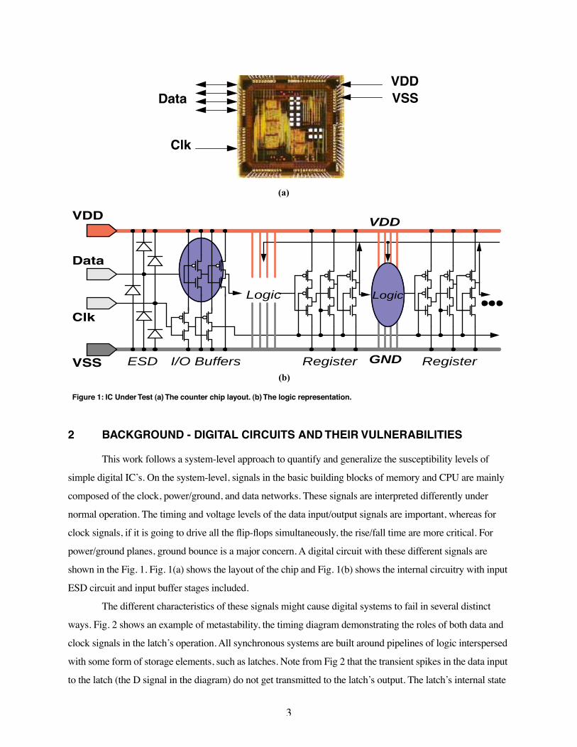
power/ground planes, ground bounce is a major concern. A digital circuit with these different signals are
shown in the Fig. 1. Fig. 1(a) shows the layout of the chip and Fig. 1(b) shows the internal circuitry with input
ESD circuit and input buffer stages included.
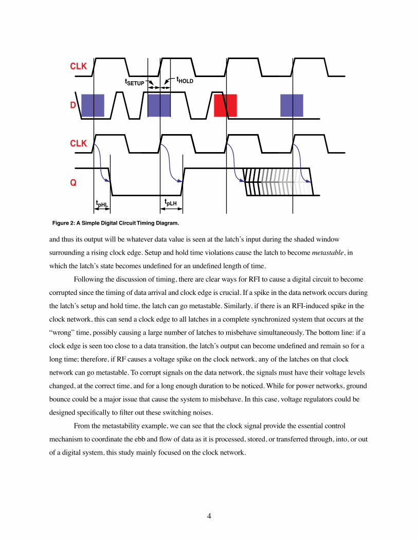
The different characteristics of these signals might cause digital systems to fail in several distinct
ways. Fig. 2 shows an example of metastability, the timing diagram demonstrating the roles of both data and
clock signals in the latch’s operation. All synchronous systems are built around pipelines of logic interspersed
with some form of storage elements, such as latches. Note from Fig 2 that the transient spikes in the data input
to the latch (the D signal in the diagram) do not get transmitted to the latch’s output. The latch’s internal state
Data
Clk
VDD VSS
(a)
Figure 1: IC Under Test (a) The counter chip layout. (b) The logic representation.
Register
Data
Clk
ESD
VDD
VSS
Logic
RegisterI/O Buffers
Logic
VDD
GND(b)
4
and thus its output will be whatever data value is seen at the latch’s input during the shaded window
surrounding a rising clock edge. Setup and hold time violations cause the latch to become
metastable
, in
which the latch’s state becomes undefined for an undefined length of time.
Following the discussion of timing, there are clear ways for RFI to cause a digital circuit to become
corrupted since the timing of data arrival and clock edge is crucial. If a spike in the data network occurs during
the latch’s setup and hold time, the latch can go metastable. Similarly, if there is an RFI-induced spike in the
clock network, this can send a clock edge to all latches in a complete synchronized system that occurs at the
“wrong” time, possibly causing a large number of latches to misbehave simultaneously. The bottom line: if a
clock edge is seen too close to a data transition, the latch’s output can become undefined and remain so for a
long time; therefore, if RF causes a voltage spike on the clock network, any of the latches on that clock
network can go metastable. To corrupt signals on the data network, the signals must have their voltage levels
changed, at the correct time, and for a long enough duration to be noticed. While for power networks, ground
bounce could be a major issue that cause the system to misbehave. In this case, voltage regulators could be
designed specifically to filter out these switching noises.
From the metastability example, we can see that the clock signal provide the essential control
mechanism to coordinate the ebb and flow of data as it is processed, stored, or transferred through, into, or out
of a digital system, this study mainly focused on the clock network.
Figure 2: A Simple Digital Circuit Timing Diagram.
CLK
D
Q
tpLH
CLK
tpHL
tHOLDtSETUP
5
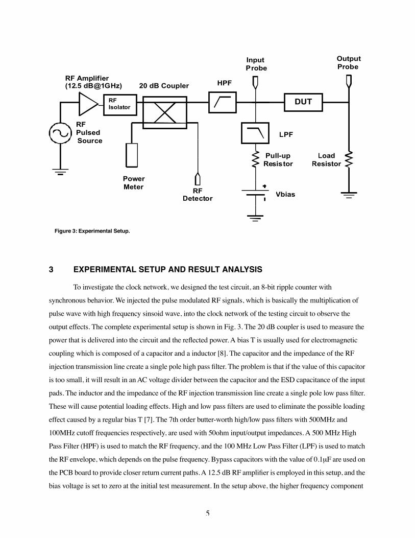
3 EXPERIMENTAL SETUP AND RESULT ANALYSIS
To investigate the clock network, we designed the test circuit, an 8-bit ripple counter with
synchronous behavior. We injected the pulse modulated RF signals, which is basically the multiplication of
pulse wave with high frequency sinsoid wave, into the clock network of the testing circuit to observe the
output effects. The complete experimental setup is shown in Fig. 3. The 20 dB coupler is used to measure the
power that is delivered into the circuit and the reflected power. A bias T is usually used for electromagnetic
coupling which is composed of a capacitor and a inductor [8]. The capacitor and the impedance of the RF
injection transmission line create a single pole high pass filter. The problem is that if the value of this capacitor
is too small, it will result in an AC voltage divider between the capacitor and the ESD capacitance of the input
pads. The inductor and the impedance of the RF injection transmission line create a single pole low pass filter.
These will cause potential loading effects. High and low pass filters are used to eliminate the possible loading
effect caused by a regular bias T [7]. The 7th order butter-worth high/low pass filters with 500MHz and
100MHz cutoff frequencies respectively, are used with 50ohm input/output impedances. A 500 MHz High
Pass Filter (HPF) is used to match the RF frequency, and the 100 MHz Low Pass Filter (LPF) is used to match
the RF envelope, which depends on the pulse frequency. Bypass capacitors with the value of 0.1
µ
F are used on
the PCB board to provide closer return current paths. A 12.5 dB RF amplifier is employed in this setup, and the
bias voltage is set to zero at the initial test measurement. In the setup above, the higher frequency component
Pull-upResistor
RFPulsedSource
RF Amplifier(12.5 dB@1GHz)
DUT
Vbias
LoadResistor
20 dB Coupler
LPF
HPF
PowerMeter
Input Probe
OutputProbe
RFDetector
RFIsolator
Figure 3: Experimental Setup.
6
of the pulse modulated RF signal entered into the Device Under Test (DUT), while the lower frequency
component is being measured at the input probe. Also, as we have shown in the Fig. 1, there are ESD and input
buffer at each input/output pin, so the actual signal that is actually transferred through the circuit is being
rectified and by the ESD component.
The DUT is a ripple counter and it is designed and fabricated using the AMI 0.5
µ
m process
technology through MOSIS. The operating clock of the ripple counter is driven by a multiplexer that chooses
between an internally generated clock and an external clock, an input signal to the circuit, “EXTCLK”. A
separate input signal, “CLKSEL” is used as a control signal to the multiplexer. In this study, we injected pulse-
modulated RF signals into the EXTCLK input pin, observed the effect on the ripple-counter output, and
recorded the required RF frequency and power level to trigger the output state change.
In the normal circuit operation, the ripple counter counts according to the internal clock of the chip.
Once we ensured the chip was working properly using the internal clock, we injected a pulse-modulated small
RF signal, with pulse width of 10
µ
sec and 1 msec pulse period into the EXTCLK input pin of the chip. We
observed the counter outputs. The reason for using pulsed RF instead of continuous wave is because the total
energy of a pulsed RF signal is adjustable. When RF pulses are applied with a relatively low duty cycle, one
percent in the setup, the total energy is much lower compared to continuous wave RF signals. This prevents the
circuit from overheating and potential damage to RF signal generator and RF amplifiers caused by the
reflected power. As we described earlier in the paper, the purpose of this study is first, to find out the circuit
input impedance characteristic of the pins of our interests; and second, based on which to investigate the power
level and frequency range to which the counter is most sensitive — i.e., those frequencies and power levels
that cause output state changes. Following the experimental setup in Fig. 3, we measured the power at each
port of the coupler at frequency range from 800MHz to 2 GHz, out of which there are no obvious state
changes observed with the amplifier employed (due to the limitation of the safe operating range of the RF
amplifier.
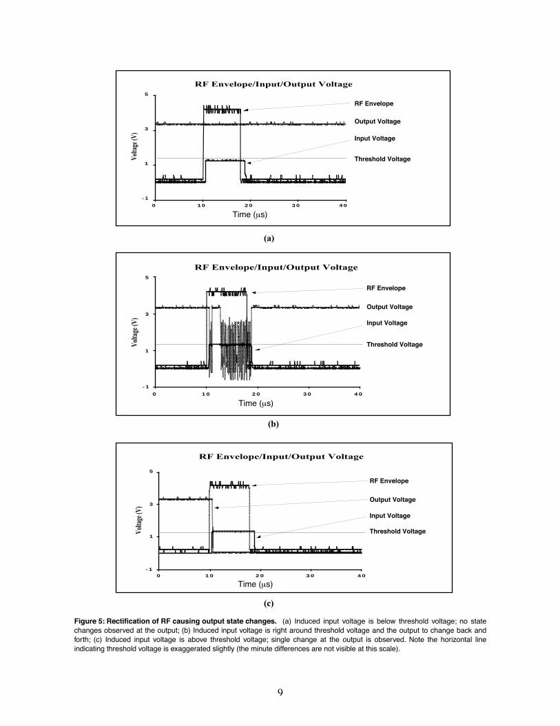
For different frequency and power levels of the injected RF signal, we observed the least significant
bit of the ripple counter output. When RF pulses were coupled into the input EXTCLK pin of the counter, we
noticed clear state changes at the output, as shown in Fig. 5(c), for a source frequency of 1.0 GHz.
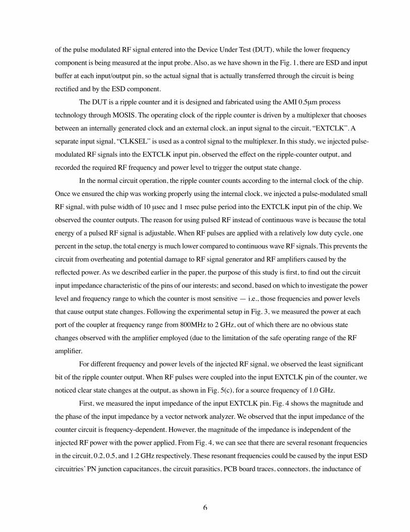
First, we measured the input impedance of the input EXTCLK pin. Fig. 4 shows the magnitude and
the phase of the input impedance by a vector network analyzer. We observed that the input impedance of the
counter circuit is frequency-dependent. However, the magnitude of the impedance is independent of the
injected RF power with the power applied. From Fig. 4, we can see that there are several resonant frequencies
in the circuit, 0.2, 0.5, and 1.2 GHz respectively. These resonant frequencies could be caused by the input ESD
circuitries’ PN junction capacitances, the circuit parasitics, PCB board traces, connectors, the inductance of
7
the wires between the die and the package (this inductance often causes a peak of high impedance in the
supply at the resonance frequency of the chip capacitance and the package inductance), supply spikes [8],
bonding pads and bonding wires.Since noise is mostly around the range of several hundred MHz, we are
working on shifting these resonant frequencies to higher frequency ranges by designing a new PCB board with
on-board SMA connectors directly connected to the test pins and with increased on-chip capacitors to have a
better matching impedance. So, in this experiment, we primarily focused on the resonant frequency that is
above 1 GHz, which is around 1.2GHz. Therefore, we injected modulated RF with carrier frequencies of 1.0 -
1.3GHz into the external clock pin. The pulse width and pulse period remained the same. We observed output
state changes which demonstrated that the input voltage was high enough to trigger the counter output to
switch. Table. 1 summarizes the RF power levels that are required to make such state changes. The table
includes the injected power; the reflected power caused by the mismatched input impedance; and the power
that was actually delivered into the pin. The last row in the table is the power-reflection coefficient
Γ
, which is
defined as square root of the reflected power over injected power. The frequency which the circuit is most
susceptible (i.e., that which requires the least power to make a state change, 1.2 GHz with the frequency range
we tested), coincides with the lowest power-reflection coefficient. This coefficient is less than half than those
at other frequency ranges, as we can see from the Table 1. This is caused by the input circuitry resonant
frequency, 1.2 GHz from Fig. 4, at which less power is required to make a state change.
We also recorded the output behavior right around the threshold power levels. The output shows full
state changes, partial state changes, and oscillations shown in the Fig. 5. In Fig. 5, the input, RF envelope, and
output voltage waveforms at RF carrier frequency of 1 GHz with pulse width 10
µ
s and pulse period 1ms are
Figure 4: Input Impedance of DUT.
8
shown. In Fig. 5 (c), the circuit exhibits output state changes when a relatively small amount of RF power, 20.5
dBm, is injected. At this point, the induced input voltage to the circuit is higher than the device threshold
voltage, therefore triggers the counter output to a complete switch. This is due to the rectification and the
amplification of the RF caused by the junction of the diode in the ESD protection circuit [4][5]. The ESD
rectification amplifies the input signal seen at the pin and induces DC voltages on the P-N junctions of ESD
protection circuit. If this induced DC voltage is higher than the threshold voltage of the circuit, injected pulse
modulated RF envelope is interpreted as a valid signal and causes a state change at the outputs. In Fig. 5(a),
when the induced DC voltage is below the threshold voltage of the circuit,with 18.1dBm injected RF power,
there is not enough input voltage to trigger the output to make a state change. In Fig. 5(b), we increased the RF
level to 20.1dBm, so that the induced DC voltage at the input pin is close to the device threshold voltage.
When the induced DC voltage is right around the threshold voltage, the noises from different resources, such
as power supplies and cables, are coupled with the input, and play a major role in the switching activities of the
output. These noise spikes superimposed on the top of the input, triggering the circuit output to switch back
and forth causing oscillations.
4 SPICE SIMULATION RESULTS
In the previous section, we had shown how the circuit behaved when we injected the external clock pin with
1GHz pulsed modulated RF. Fig. 5(a) shows no output change behavior at all. The graphs Fig.5 (b) and (c)
have different output switching behavior and therefore raise questions about what is causing the behavior. For
instance, Fig. 5 (c) shows the circuit responding only to the envelope of the RF (the leading edge). Is this
because the RF frequency is too high for the circuit to respond, or is the RF frequency able to drive the circuit,
but the circuit is put into metastability and requires a correctly-timed clock edge to be driven out? Similarly,
Table 1: Power required to make state changes (dBm)
Frequency (GHz): 1.0 1.1 1.2 1.3
Injected Power (dBm): 20.1 17.9 16.9 20.5
Reflected Power (dBm): 13.3 13.8 6.3 15.3
Delivered Power (dBm): 16.8 15.2 14.7 16.6
Power Reflection Coefficient Γ
0.56 0.65 0.39 0.65
9
RF Envelope/Input/Output Voltage
-1
1
3
5
0 10 20 30 40
Time (µs)
Voltage (V)
RF EnvelopeOutput VoltageInput Voltage
Figure 5: Rectification of RF causing output state changes. (a) Induced input voltage is below threshold voltage; no statechanges observed at the output; (b) Induced input voltage is right around threshold voltage and the output to change back andforth; (c) Induced input voltage is above threshold voltage; single change at the output is observed. Note the horizontal lineindicating threshold voltage is exaggerated slightly (the minute differences are not visible at this scale).
RF Envelope/Input/Output Voltage
-1
1
3
5
0 10 20 30 40
Time (µs)
Voltage (V) Output Voltage
Input VoltageRF Envelope
RF Envelope/Input/Output Voltage
-1
1
3
5
0 10 20 30 40
Time (µs)
Voltage (V)
RF EnvelopeInput VoltageOutput Voltage
(a)
(b)
(c)
RF Envelope
Output Voltage
Input Voltage
Threshold Voltage
Output Voltage
Threshold Voltage
RF Envelope
Input Voltage
Output Voltage
Threshold Voltage
RF Envelope
Input Voltage
Time (µs)
Time (µs)
Time (µs)
10
Fig. 5(b) shows the circuit responding to much more than just the envelope of the RF: Is it responding to the
noise on top of the clock signal? or to the actual RF signal that went through the circuit? or to the input
resonant frequencies? Also, note that the frequency of the output response in Fig. 5(b) is much less than the
frequency of the RF input. Does this suggest that one might be able to rule out the RF signal as the cause for
the behavior (leaving noise as the most likely explanation)? With all these doubts in mind, we performed some
SPICE simulations to try to understand these mechanisms, answer these questions, and rule out one or more
causes.
Since our DUT is basically a series of cascaded flip-flops, we choose a single filp-flop as our SPICE
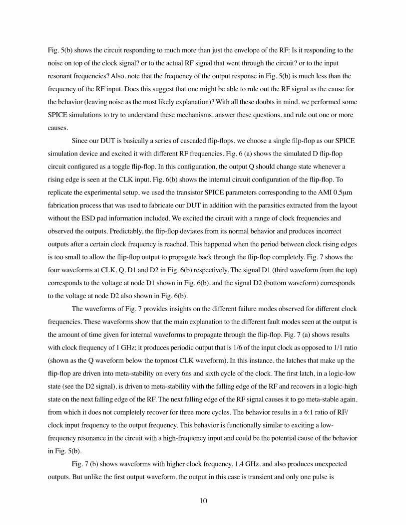
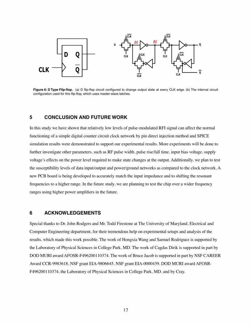
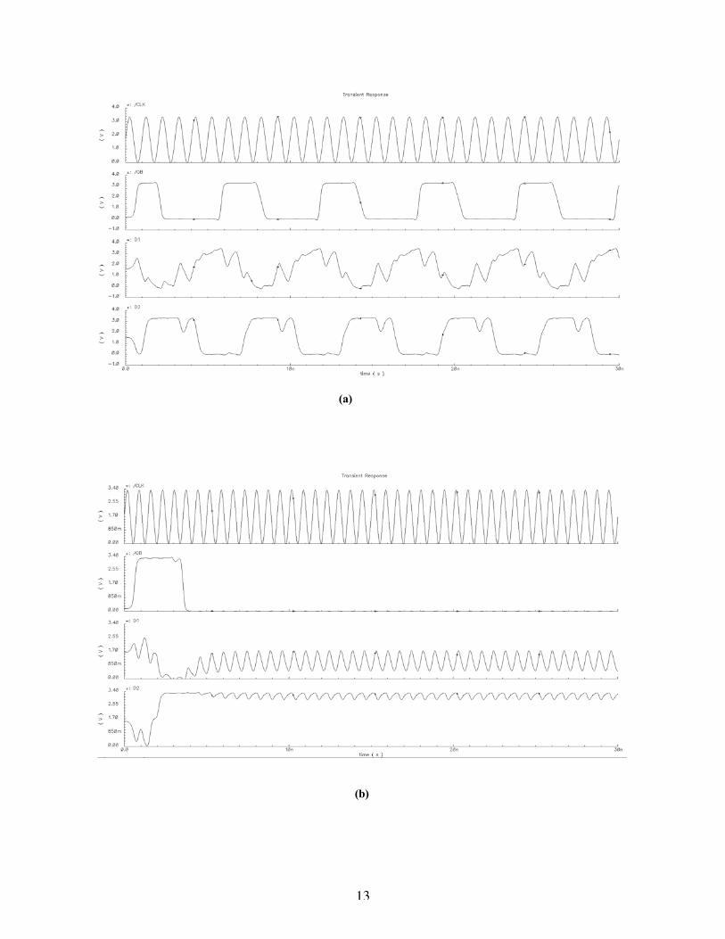
simulation device and excited it with different RF frequencies. Fig. 6 (a) shows the simulated D flip-flop
circuit configured as a toggle flip-flop. In this configuration, the output Q should change state whenever a
rising edge is seen at the CLK input. Fig. 6(b) shows the internal circuit configuration of the flip-flop. To
replicate the experimental setup, we used the transistor SPICE parameters corresponding to the AMI 0.5
µ
m
fabrication process that was used to fabricate our DUT in addition with the parasitics extracted from the layout
without the ESD pad information included. We excited the circuit with a range of clock frequencies and
observed the outputs. Predictably, the flip-flop deviates from its normal behavior and produces incorrect
outputs after a certain clock frequency is reached. This happened when the period between clock rising edges
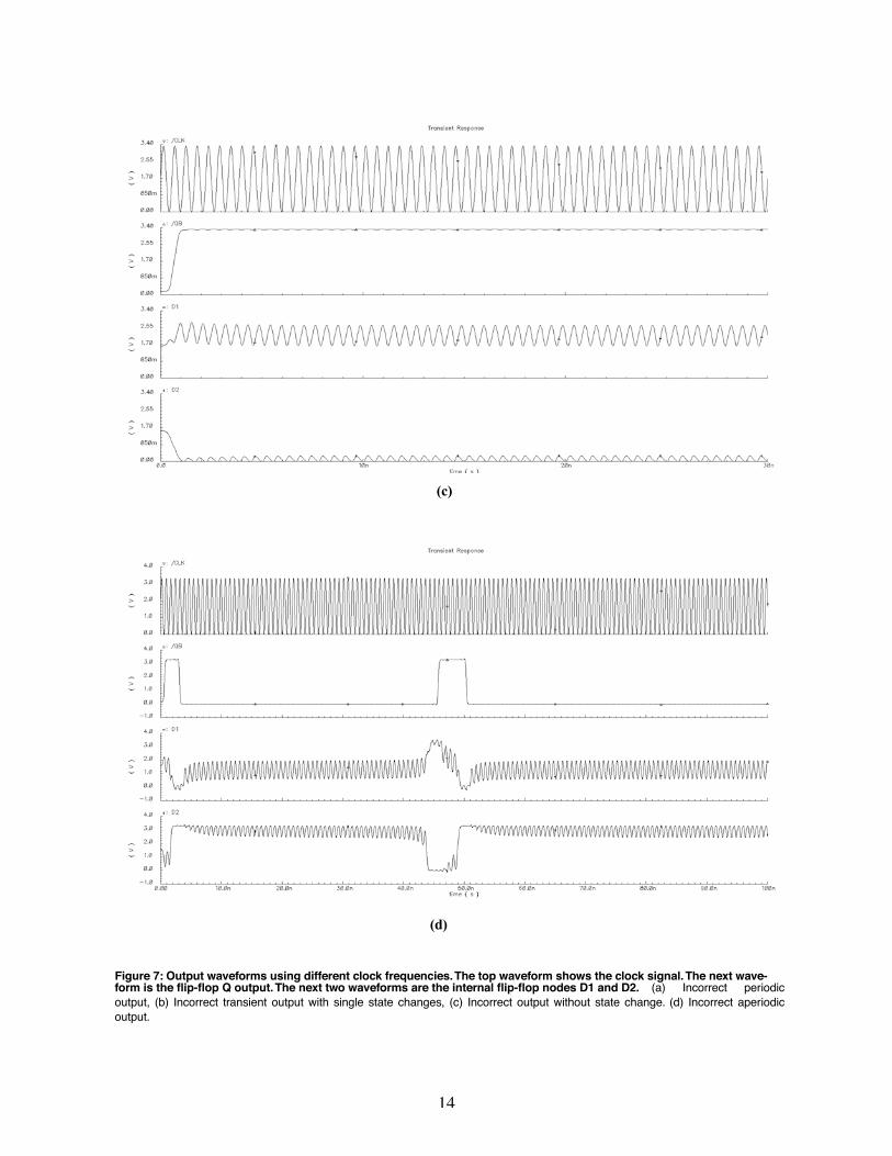
is too small to allow the flip-flop output to propagate back through the flip-flop completely. Fig. 7 shows the
four waveforms at CLK, Q, D1 and D2 in Fig. 6(b) respectively. The signal D1 (third waveform from the top)
corresponds to the voltage at node D1 shown in Fig. 6(b), and the signal D2 (bottom waveform) corresponds
to the voltage at node D2 also shown in Fig. 6(b).
The waveforms of Fig. 7 provides insights on the different failure modes observed for different clock
frequencies. These waveforms show that the main explanation to the different fault modes seen at the output is
the amount of time given for internal waveforms to propagate through the flip-flop. Fig. 7 (a) shows results
with clock frequency of 1 GHz; it produces periodic output that is 1/6 of the input clock as opposed to 1/1 ratio
(shown as the Q waveform below the topmost CLK waveform). In this instance, the latches that make up the
flip-flop are driven into meta-stability on every 6ns and sixth cycle of the clock. The first latch, in a logic-low
state (see the D2 signal), is driven to meta-stability with the falling edge of the RF and recovers in a logic-high
state on the next falling edge of the RF. The next falling edge of the RF signal causes it to go meta-stable again,
from which it does not completely recover for three more cycles. The behavior results in a 6:1 ratio of RF/
clock input frequency to the output frequency. This behavior is functionally similar to exciting a low-
frequency resonance in the circuit with a high-frequency input and could be the potential cause of the behavior
in Fig. 5(b).
Fig. 7 (b) shows waveforms with higher clock frequency, 1.4 GHz, and also produces unexpected
outputs. But unlike the first output waveform, the output in this case is transient and only one pulse is
11
produced. Fig. 5(c) shows the counter circuit responding initially to the RFI, but only for a single state-change
which is corresponding to Fig. 7(b) suggesting again that RF reaching the circuit could be the cause of the
observed output. Fig. 7(b) shows that the internal latch (D2) fails to recover from the second metastable
instance. The internal latch is driven from a mid-point logic value into metastability and ultimately falls to
logic-low. Fig. 7(c) shows an even simpler scenario with frequency of 1.8 GHz, one in which the first hint of a
clock signal (RF) changes the state of the circuit, but the RF cycle time is too short for the inverters to switch
completely, resulting in the familiar saw-tooth waveform in D1. These two graphs show that the behavior in
Fig. 5(c) could be caused by high-frequency RF reaching the circuit (frequencies too high for the circuit to
respond) high enough to make the circuit difficult to come out of metastability.
Fig. 5(b) could be easily seen as potentially caused by noise on top of the input signal(note that the
brief period of logic-high during the window of output corresponds to a brief window of lessened noise in the
Input Voltage signal). However, we can’t exclude the possibility that the output could also be caused by the
regular RF input forcing the circuit to behave in an irregular manner. Fig. 7(d) shows an example of a
continuous-wave clock input fed into the flip-flop, with frequency of 1. 355 GHz, yielding an aperiodic output
with two pulse train. One interesting thing to point out is that the clock frequencies that generate aperiodic
output and periodic output differ by only 2 MHz, which means that at 1.333 GHz, the output is periodic,
similar to the 1GHz one; while at 1.335 GHz, we observed the aperiodic pulses. This behavior shows that with
the increasing of the clock frequency, the output failure modes change from periodic, to aperiodic, to barely
triggering the output with one pulse and finally to not triggering the output at all.
In all, while signal noise could very well cause the behavior in Fig. 5(b), it could just as easily be the
regular RF itself combined with these irregularity shown in Fig. 7(d). In summary, it is not clear whether the
input noise, a (possibly rectified) periodic RF signal passes all the way to the circuit combined with aperiodic
output shown as Fig. 7(d) or the behavior shown in the Fig. 7(a) cause the behavior seen in Fig. 5(b). If the RF
is successfully filtered out by the ESD circuitry, leaving a simple DC bias, then noise on that signal could be
the major cause the observed behavior.
These simulations provide intuitive views of our experimental results. In the future work, we will
address these questions in more detail by investigating the counter circuit behaviors under different frequency
ranges in the physical experiment setup we used.
12
5 CONCLUSION AND FUTURE WORK
In this study we have shown that relatively low levels of pulse-modulated RFI signal can affect the normal
functioning of a simple digital counter circuit clock network by pin direct injection method and SPICE
simulation results were demonstrated to support our experimental results. More experiments will be done to
further investigate other parameters, such as RF pulse width, pulse rise/fall time, input bias voltage, supply
voltage’s effects on the power level required to make state changes at the output. Additionally, we plan to test
the susceptibility levels of data input/output and power/ground networks as compared to the clock network. A
new PCB board is being developed to accurately match the input impedance and to shifting the resonant
frequencies to a higher range. In the future study, we are planning to test the chip over a wider frequency
ranges using higher power amplifiers in the future.
6 ACKNOWLEDGEMENTS
Special thanks to Dr. John Rodgers and Mr. Todd Firestone at The University of Maryland, Electrical and
Computer Engineering department, for their tremendous help on experimental setups and analysis of the
results, which made this work possible. The work of Hongxia Wang and Samuel Rodriguez is supported by
the Laboratory of Physical Sciences in College Park, MD. The work of Cagdas Dirik is supported in part by
DOD MURI award AFOSR-F496200110374. The work of Bruce Jacob is supported in part by NSF CAREER
Award CCR-9983618, NSF grant EIA-9806645, NSF grant EIA-0000439, DOD MURI award AFOSR-
F496200110374, the Laboratory of Physical Sciences in College Park, MD, and by Cray.
Figure 6: D Type Filp-flop. (a) D flip-flop circuit configured to change output state at every CLK edge. (b) The internal circuitconfiguration used for this flip-flop, which uses master-slave latches.
13
(a)
(b)
14
Figure 7: Output waveforms using different clock frequencies. The top waveform shows the clock signal. The next wave-form is the flip-flop Q output. The next two waveforms are the internal flip-flop nodes D1 and D2. (a) Incorrect periodicoutput, (b) Incorrect transient output with single state changes, (c) Incorrect output without state change. (d) Incorrect aperiodicoutput.
(c)
(d)
15
7 REFERENCES
[1] F. Fiori, “Integrated Circuit Susceptibility to Conducted RF Interference”, Compliance Engineering17, no. 8 (2000), pp. 40-49.
[2] S. Baffreau, S. Bendhia, M. Ramdani, E.Sicard, “Characterisation of Microcontroller Susceptibilityto Radio Frequency Interference”, Proc. of the Fourth IEEE International Caracas Conference on De-vices, Circuits and Systems, 17-19 April 2002, pp. I031-1 -I031-5.
[3] F. Fiori, S. Benelli, G. Gaidano, V. Pozzolo, “Investigation on VLSI’s Input Ports Susceptibility toConducted RF Interference”, IEEE International Symposium on Electromagnetic Compatibility, 18-22 Aug. 1997, pp. 326 -329.
[4] D. J. Kenneally, D.S. Koellen, S. Epshtein, “RF Upset Susceptibility of CMOS and Low PowerSchottky D-Type, Flip-Flops”, IEEE National Symposium on Electromagnetic Compatibility, 23-25May 1989, pp. 190 -195.
[5] J. Rodgers, T. M. Firestone, V. L. Granatstein, “Nonlinear Effects in Advanced Communication Cir-cuits Excited by Pulsed RF”, http://www.ireap.umd.edu/MURI-2001/Review_14Nov03/10_rodgers.pdf.
[6] J. G. Tront, “Predicting URF Upset of MOSEFET Digital I C’s”, IEEE Transactions on Electromag-netic Compatibility, Volume, EMC-27, Mo.2, May 1985.
[7] Todd Firestone, “RF Induced Non-Linear Effects in High-Speed Electronics”, Thesis, University ofMaryland, College Park, 2004.
[8] E. Sicard, C. Marot, J. Y. Fourniols, M. Randani, “Electromagnetic Compatibility for Integrated Cir-cuits”, Contribution to book IEEE Review of radio Sciences 1998-2001 URSI, IEEE Press-ISBN 0-471-26866-6, 2002.