Embed Size (px)
DESCRIPTION
Electromagnetic Interference
Citation preview

EMI in power suppliesEMI in power supplies
Alfred HesenerFairchild Semiconductor Europe
www.fairchildsemi.com
Agenda
• Introduction• Different types of EMI and their characteristicsDifferent types of EMI and their characteristics• Regulations and standards for EMI• Measurement and sources of EMI
• Conducted EMI• Radiated EMI
• EMI as integral part of the design flow• Conclusion
www.fairchildsemi.comCompany Confidential Page 2
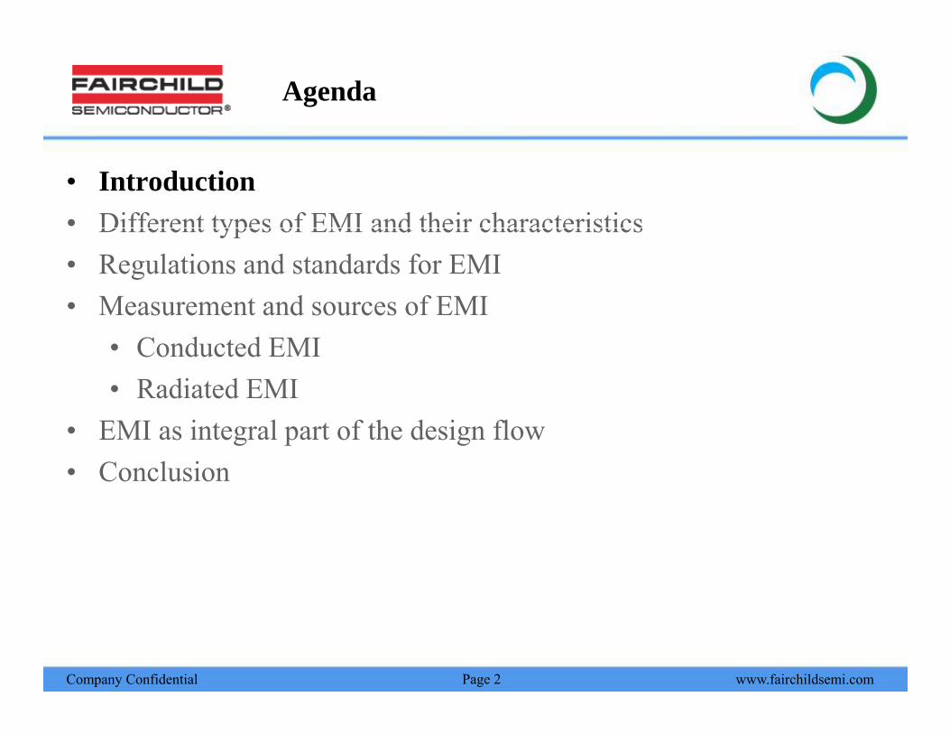
IntroductionEMI more and more complex
• Increasing power density, faster switching, higher currents are causing more EMI-related issuesg• Conducted / radiated EMI
• Further changes complicating things• New semiconductor switches are faster• New topologies (e.g. Quasi-resonant)
hi “ b ” d i ?• How to achieve a “robust” design?• Embed EMI into the design flow from the beginning
• What is the goal?• What is the goal?• Emit low EMI levels to meet regulations (don’t disturb other
applications nearby) EMI compliance
www.fairchildsemi.comCompany Confidential
• Work properly (be self-compliant) Robustness
Page 3

Agenda
• Introduction• Different types of EMI and their characteristicsDifferent types of EMI and their characteristics• Regulations and standards for EMI• Measurement and sources of EMI
• Conducted EMI• Radiated EMI
• EMI as integral part of the design flow• Conclusion
www.fairchildsemi.comCompany Confidential Page 4

Different types of EMI and their characteristics
Emitter “Reduce emission of source”
Galvanic Wave
“Reduce transmission
GalvanicCoupling Capacitive
CouplingInductiveCoupling
WaveCoupling
in the system”
Receiver
Galvanic coupling of Electric field Magnetic field Radiated wave traveling in the
“Reduce sensitivity of receiver”
Galvanic coupling of signals in the circuit
Electric field Magnetic field Radiated wave traveling in the system
Typically <30MHz Medium-high frequencies
Typically > 30MHz High frequencies
An nois signal in the Large dV/dt Large dI/dt Fast s itching
www.fairchildsemi.comCompany Confidential
Any noisy signal in the system
Large dV/dt Large dI/dt Fast switching
(RC) filtering Metal shield Magnetic shield Electromagnetic shieldPage 5
Agenda
• Introduction• Different types of EMI and their characteristicsDifferent types of EMI and their characteristics• Regulations and standards for EMI• Measurement and sources of EMI
• Conducted EMI• Radiated EMI
• EMI as integral part of the design flow• Conclusion
www.fairchildsemi.comCompany Confidential Page 6

Regulations and standard for EMIEN550xx and EN61000 most important
• Two main considerations:• Limit the amount of emission which a given application generates• Define minimum immunity levels a given application must tolerateDefine minimum immunity levels a given application must tolerate
• EN550xx – the “EMI” norm (class A = “consumer”, class B = “industrial”)• CISPR11, EN55011 for industrial, medical, scientific applications• CISPR13, EN55013 for consumer applications
CISPR14 EN55014 f h li t l i l i ti t l• CISPR14, EN55014 for home appliances, power tools, involving motion control• CISPR15, EN55015 for lighting equipment• CISPR22, EN55022 for computing applications• CISPR16, EN55016 defines the measurement method
• Many applications being tested against a “mix” of different norms (e.g. EN55022 for frequencies >150kHz, EN55015 for frequencies <150kHz)
• EN61000 – the “PFC” norm (equipment classes see next page)• Noise current up to the 40th harmonic of the line frequency ( <= 2 0kHz (e g EU) / 2 4kHz (e g US))• Noise current up to the 40 harmonic of the line frequency ( <= 2.0kHz (e.g. EU) / 2.4kHz (e.g. US))• EN61000-3-2 for applications < 16A• EN61000-3-12 for applications with 16A…75A• EN61000-4-7 defines the measurement and evaluation method• EN61000 4 16 for common mode disturbances up to 150kHz
www.fairchildsemi.comCompany Confidential
• EN61000-4-16 for common-mode disturbances up to 150kHz• Many further standards exist, dealing with more specialized applications• EN61000 specifies maximum harmonic currents, not a power factor
Page 7
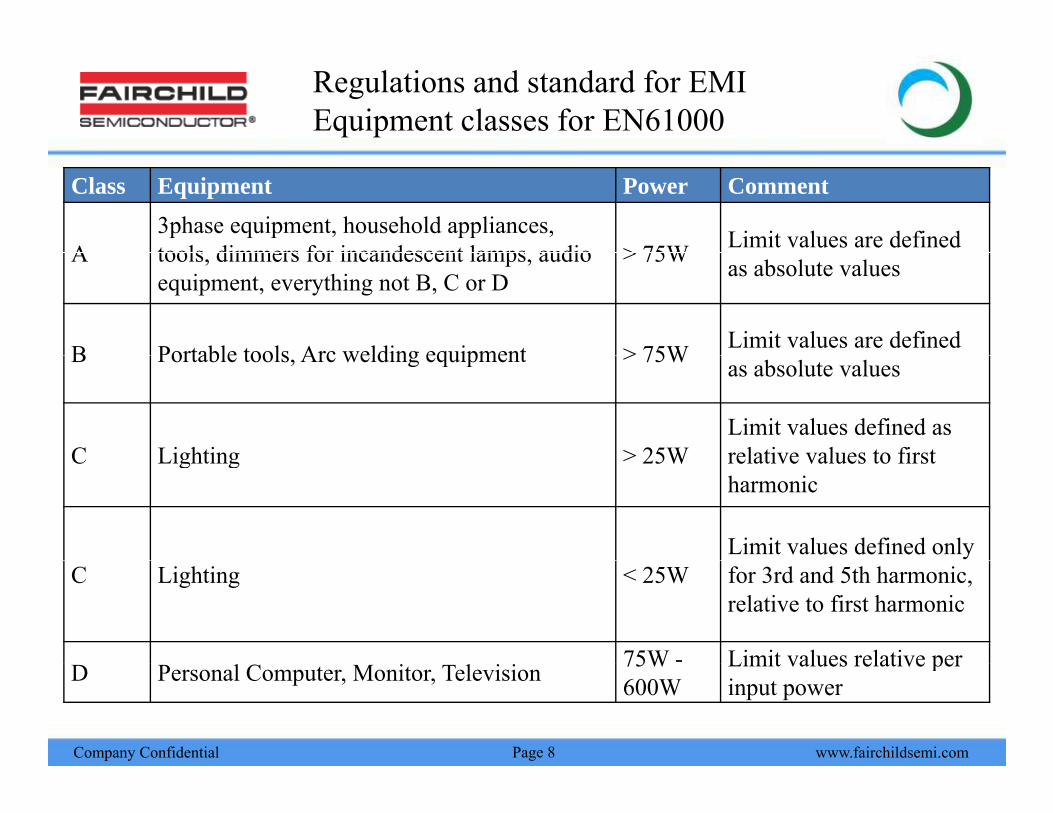
Regulations and standard for EMIEquipment classes for EN61000
Class Equipment Power Comment
A3phase equipment, household appliances, tools dimmers for incandescent lamps audio > 75W Limit values are defined A tools, dimmers for incandescent lamps, audio equipment, everything not B, C or D
> 75W as absolute values
B Portable tools Arc welding equipment > 75W Limit values are defined B Portable tools, Arc welding equipment > 75W as absolute values
C Lighting > 25WLimit values defined as relative values to firstC Lighting > 25W relative values to first harmonic
Limit values defined only C Lighting < 25W for 3rd and 5th harmonic,
relative to first harmonic
75W - Limit values relative per
www.fairchildsemi.comCompany Confidential
D Personal Computer, Monitor, Television 75W 600W
Limit values relative per input power
Page 8

The power factorSimulation results
• Simulation shows input and bus cap voltage, and current spikes in the input• High dI/dt illustrates significant harmonic content • Simulation below is 100W class A SMPS would require a (active) PFCSimulation below is 100W class A SMPS, would require a (active) PFC
• EN61000 considers harmonics to 2kHz/2.4kHz – this would be a pretty large filter if realized with passive components
• Attenuation of this filters’ components for higher frequencies (conducted EMI) p g q ( )would be low, due to potentially high parasitic capacitance, and it may not help with CM noise at all
Limit values for EN61000 class D
www.fairchildsemi.comCompany Confidential Page 9

Agenda
• Introduction• Different types of EMI and their characteristicsDifferent types of EMI and their characteristics• Regulations and standards for EMI• Measurement and sources of EMI
• Conducted EMI• Radiated EMI
• EMI as integral part of the design flow• Conclusion
www.fairchildsemi.comCompany Confidential Page 10

Measurement and sources of EMIConducted EMI test setup
Line Impedance Stabilizer Network (“LISN”):- Defined impedance for noise voltage measurement
www.fairchildsemi.comCompany Confidential
- Blocking the noise coming from the grid
Page 11

Measurement and sources of EMIConducted EMI limits
Vertical: Amplitude in dbuVHorizontal: Frequency in MHzSolid blue line: EN55011/22 limits for averageSolid red line: EN55022 limits for quasipeakRed spectrum line: quasipeak measurement valuesRed spectrum line: quasipeak measurement valuesBlack spectrum line: average measurement values
Frequency range
Bandwidth (-6dB)
Frequency Limit (dbuV) Limit (V) Comment9kHz ... 50kHz 110 316mVEN55011 Quasipeak
50kHz ... 150kHz 90 ... 80 32mV ... 10mVEN55011 QuasipeakEN55022 B Quasi peak; linearly falling 9kHz ...
150kHz200 Hz
150kHz ... 30MHz
9 kHz
150kHz ... 500kHz66 ... 56 2mV ... 0.63mVEN55022 B, Quasi-peak; linearly falling
with log (frequency)
56 ... 46 0.63mV ... 0.2mVEN55022 B, Average; linearly falling with log (frequency)
0.5MHz ... 5MHz 56 630uVEN55022 B, Quasi-peak 46 200uVEN55022 B, Average
www.fairchildsemi.comCompany Confidential
30MHz ... 1GHz
120kHz5MHz ... 30MHz 60 1mVEN55022 B, Quasi-peak
50 316uVEN55022 B, Average
Page 12

Conducted EMIDifferential and common mode noise
• In most cases, two different noise voltages will appear at nodes L and N• Separate into differential (“DM”) and common mode (“CM”) noise• Different filtering required for both noise types!
• Differential mode noise appears out of phase at the nodes• Noise current flows in a loop between L and N (“1”)Noise current flows in a loop between L and N ( 1 )
• Common mode noise appears in phase at both nodes• Noise current flows via ground and back through the lines (“2”)
L DM noise current
1
N Ground
1
2 ParasiticCoupling
www.fairchildsemi.comCompany Confidential
CM noise current
Page 13
Coupling
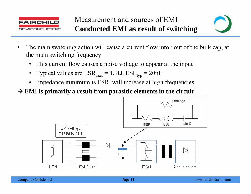
Measurement and sources of EMIConducted EMI as result of switching
• The main switching action will cause a current flow into / out of the bulk cap, at the main switching frequency• This current flow causes a noise voltage to appear at the input• Typical values are ESRmax = 1.9Ω, ESLtyp = 20nH• Impedance minimum is ESR, will increase at high frequenciesp , g q
EMI is primarily a result from parasitic elements in the circuit
www.fairchildsemi.comCompany Confidential Page 14
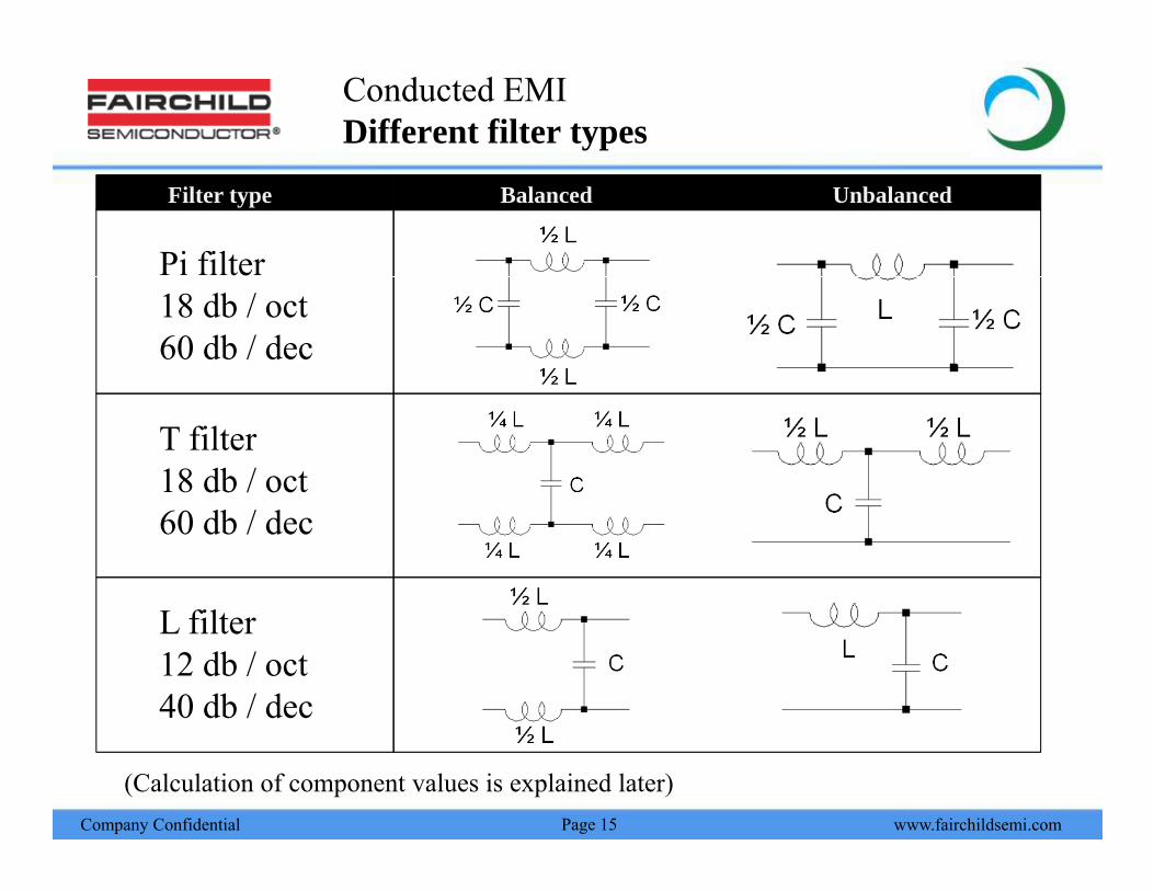
Conducted EMIDifferent filter types
Pi filter
Filter type Balanced Unbalanced
18 db / oct60 db / dec
T filter18 db / oct60 db / dec
L filtL filter12 db / oct40 db / dec
www.fairchildsemi.comCompany Confidential
(Calculation of component values is explained later)Page 15

Conducted EMICommon mode vs differential mode
• For common mode noise, the line to line capacitors do not help• Only the inductors contribute (but typically they are too small)y ( yp y y )
• Introduce a common mode choke• Designed for (large) leakage inductance to provide DM filter function
Line to
Choke (with leakageinductance)
Line toline cap
www.fairchildsemi.comCompany Confidential
Example of a 200W power supply input stage with a two-stage CM choke
Page 16
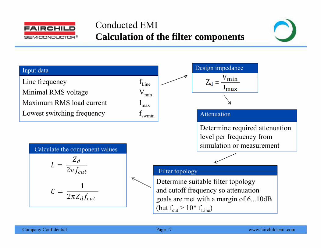
Conducted EMICalculation of the filter components
Input data Design impedance
Line frequency fLine
Minimal RMS voltage Vmin
Maximum RMS load current Imax
Lowest switching frequency fswmin Attenuation
Determine required attenuation level per frequency fromp q ysimulation or measurement
Filter topology
Calculate the component values
Determine suitable filter topologyand cutoff frequency so attenuationgoals are met with a margin of 6...10dB
Filter topology
www.fairchildsemi.comCompany Confidential
g g(but fcut > 10* fLine)
Page 17

Conducted EMISimulation and results
• Simulation for compliance: Noise generation and filter attenuation are mostly determined by parasitic elements in the circuity y p• Noise generation: Leakage inductance, ESR, ESL, capacitive
coupling (to ground)• Attenuation: Core frequency response, capacitive coupling• Most simulators allow to set parasitics for all passive
componentscomponents• Using a behavioural model for the noise (current) source is a
good approximation• Simulation for function and robustness: Very complex – better to
design accordingly, test a prototype, implement fixes in final circuit
www.fairchildsemi.comCompany Confidential Page 18

Conducted EMIExample values for parasitics
Inductor Parallel capacitancee.g. 50pF for 1mHg p
Series resistancee.g. 1.9 Ohm for 100uF
Capacitorg
Series inductancee.g. 20nH for 100uF
TransformerLeakage inductancee.g. 10uH for 200uH (prim)Parasitic capacitancee g 50pF for EF25
CM choke
e.g. 50pF for EF25
Leakage inductancee.g. 300uH for 10mHP i i i
www.fairchildsemi.comCompany Confidential
Parasitic capacitancee.g. 100pF for 10mH
Page 19
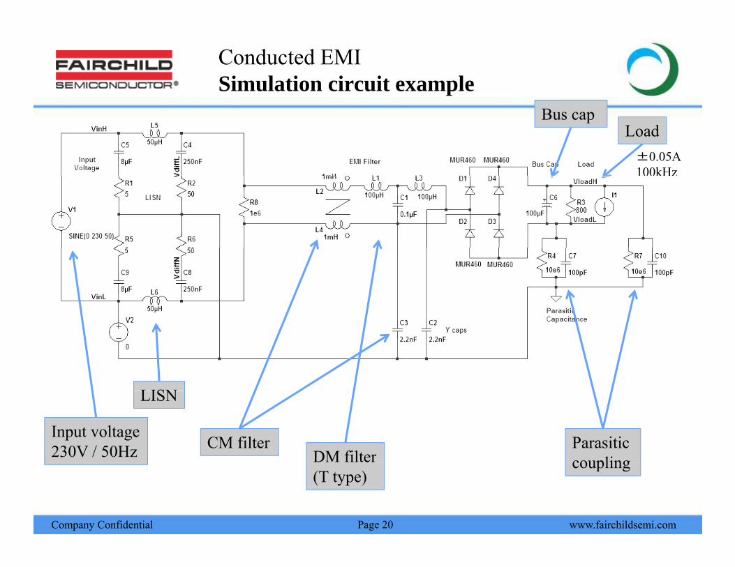
Conducted EMISimulation circuit example
LoadBus cap
±0.05A100kHz
LISN
Input voltage230V / 50Hz
LISN
CM filterDM filter
Parasiticcoupling
www.fairchildsemi.comCompany Confidential
(T type)coupling
Page 20
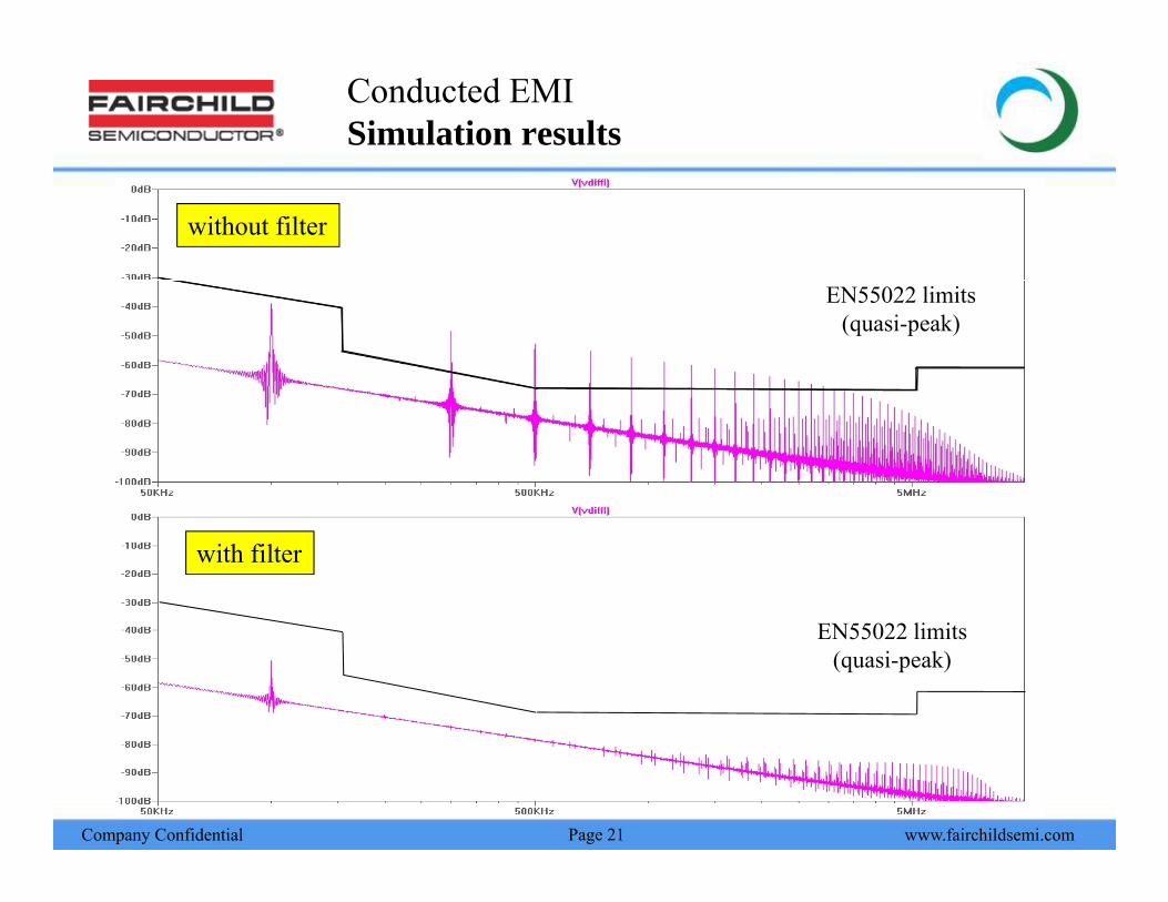
Conducted EMISimulation results
without filter
EN55022 limits(quasi-peak)
with filter
EN55022 limits(quasi-peak)
www.fairchildsemi.comCompany Confidential Page 21
Agenda
• Introduction• Different types of EMI and their characteristicsDifferent types of EMI and their characteristics• Regulations and standards for EMI• Measurement and sources of EMI
• Conducted EMI• Radiated EMI
• EMI as integral part of the design flow• Conclusion
www.fairchildsemi.comCompany Confidential Page 22
Radiated EMIWhat generates it?
• Magnetic EMI is caused by changing currents:
Current (di/dt)
R• Vnoise =
RM
RS + RM
dI
dt* M * Vnoise
+ Vmeas
R
RS
• Coupling factor M depends on:Di t d i t ti f th
RM
• Distance, area and orientation of the disturbing magnetic loops
• Magnetic absorption between the loops
www.fairchildsemi.comCompany Confidential
• Current risetime• Impedance of the receiver
Page 23
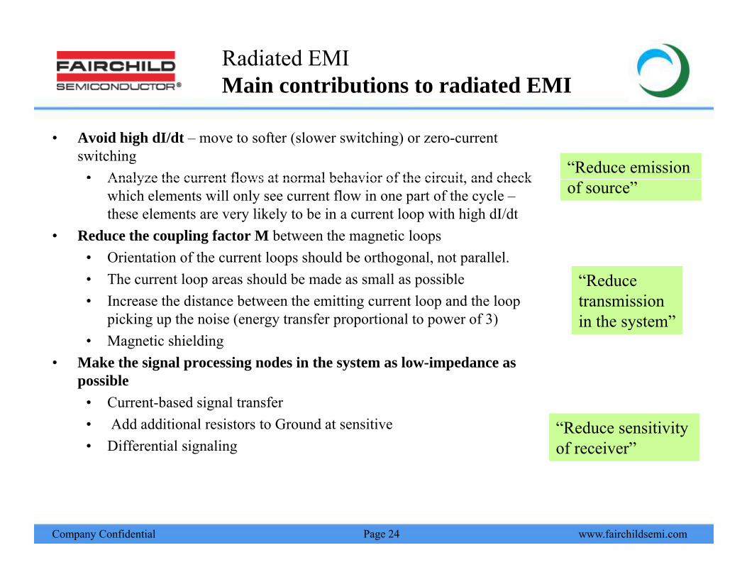
Radiated EMIMain contributions to radiated EMI
• Avoid high dI/dt – move to softer (slower switching) or zero-current switching
• Analyze the current flows at normal behavior of the circuit and check “Reduce emission Analyze the current flows at normal behavior of the circuit, and check which elements will only see current flow in one part of the cycle –these elements are very likely to be in a current loop with high dI/dt
• Reduce the coupling factor M between the magnetic loopsO i i f h l h ld b h l ll l
of source”
• Orientation of the current loops should be orthogonal, not parallel.• The current loop areas should be made as small as possible• Increase the distance between the emitting current loop and the loop
picking up the noise (energy transfer proportional to power of 3)
“Reduce transmission in the system”p g p ( gy p p p )
• Magnetic shielding• Make the signal processing nodes in the system as low-impedance as
possibleC b d i l f
in the system
• Current-based signal transfer• Add additional resistors to Ground at sensitive• Differential signaling
“Reduce sensitivity of receiver”
www.fairchildsemi.comCompany Confidential Page 24
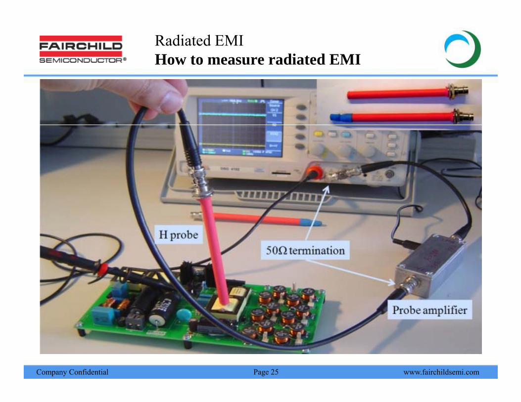
Radiated EMIHow to measure radiated EMI
www.fairchildsemi.comCompany Confidential Page 25
Radiated EMIHow to identify “hot spots”
• Use a two-channel scope• Connect a (HV) probe to the main switching signalConnect a (HV) probe to the main switching signal• Connect the H-field probe to a probe amplifier (if necessary) and to
the second channel (proper termination required)• Use the main switching signal as a trigger signal• “Wander” around the PCB to identify areas of large emission, then
zoom inzoom in• Take (static) pictures of the critical field signals to determine
frequency and quality factor (this can be used to identify the q y q y ( yelements of the resonant tanks)
www.fairchildsemi.comCompany Confidential Page 26
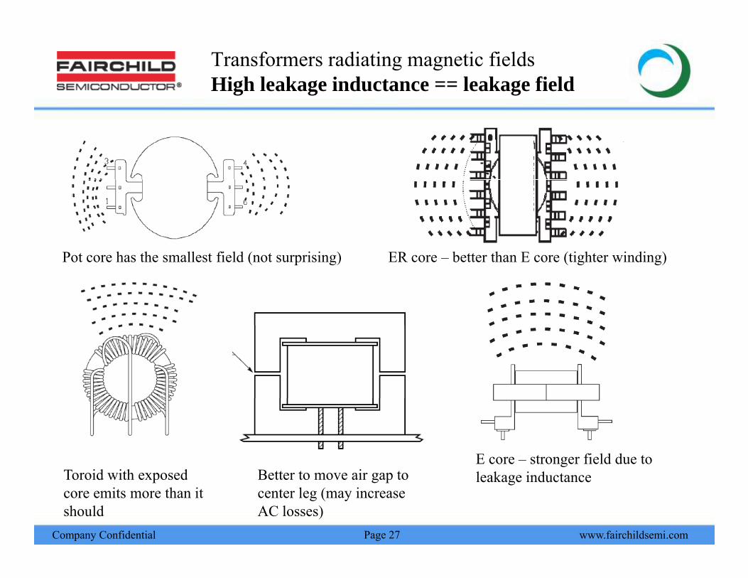
Transformers radiating magnetic fieldsHigh leakage inductance == leakage field
P h h ll fi ld ( i i ) ER b h E ( i h i di )Pot core has the smallest field (not surprising) ER core – better than E core (tighter winding)
E core – stronger field due to B tt t i tT id ith d
www.fairchildsemi.comCompany Confidential
leakage inductanceBetter to move air gap to center leg (may increaseAC losses)
Toroid with exposedcore emits more than itshould
Page 27
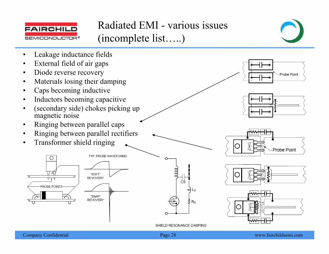
Radiated EMI - various issues(incomplete list…..)
• Leakage inductance fields• External field of air gaps• Diode reverse recovery
M i l l i h i d i• Materials losing their damping• Caps becoming inductive• Inductors becoming capacitive• (secondary side) chokes picking up ( y ) p g p
magnetic noise• Ringing between parallel caps• Ringing between parallel rectifiers• Transformer shield ringing• Transformer shield ringing
www.fairchildsemi.comCompany Confidential Page 28
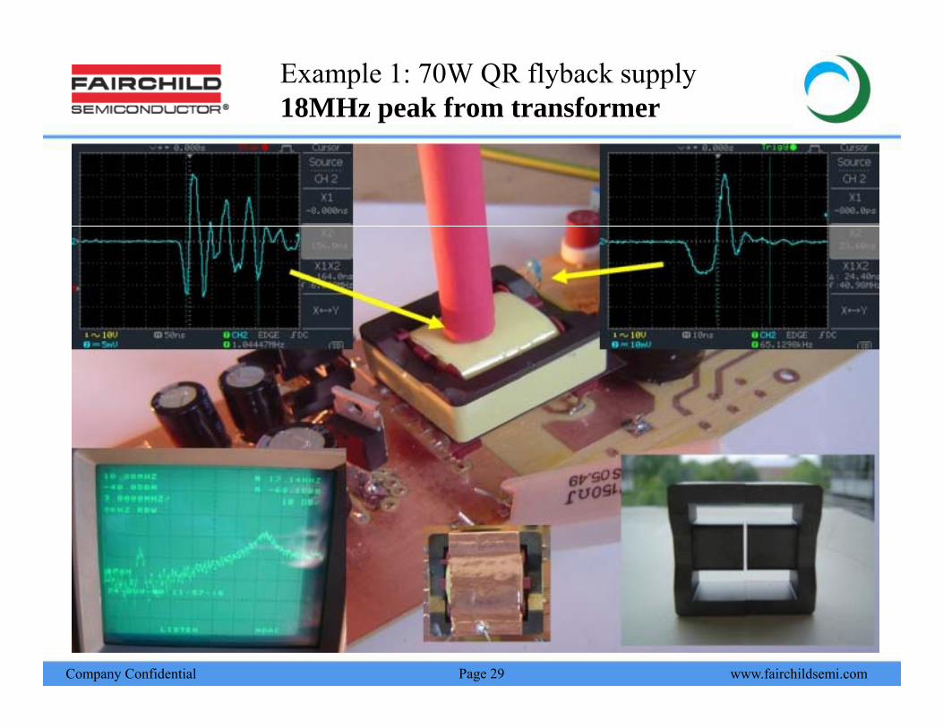
Example 1: 70W QR flyback supply18MHz peak from transformer
www.fairchildsemi.comCompany Confidential Page 29
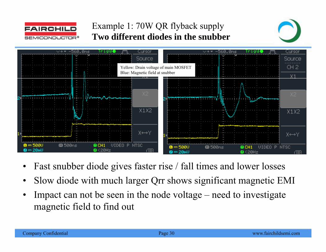
Example 1: 70W QR flyback supplyTwo different diodes in the snubber
Yellow: Drain voltage of main MOSFETBlue: Magnetic field at snubber
• Fast snubber diode gives faster rise / fall times and lower losses• Slow diode with much larger Qrr shows significant magnetic EMI• Impact can not be seen in the node voltage – need to investigate
magnetic field to find out
www.fairchildsemi.comCompany Confidential
magnetic field to find out
Page 30
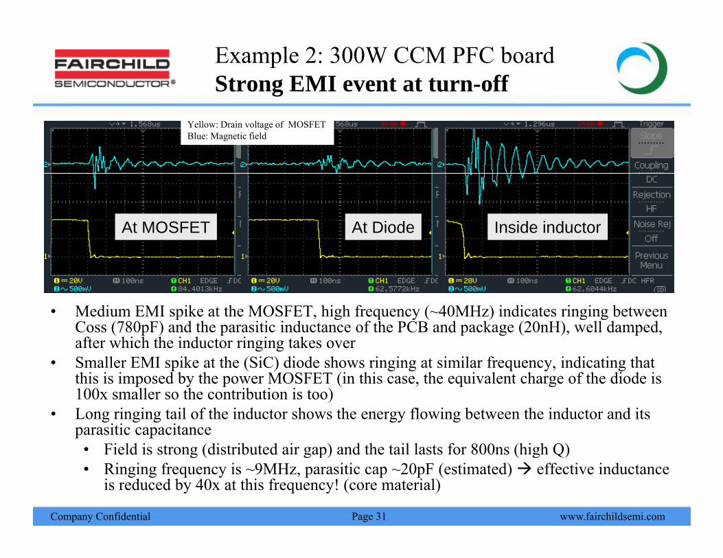
Example 2: 300W CCM PFC boardStrong EMI event at turn-off
Yellow: Drain voltage of MOSFETBlue: Magnetic field
At MOSFET At Diode Inside inductor
• Medium EMI spike at the MOSFET high frequency (~40MHz) indicates ringing betweenMedium EMI spike at the MOSFET, high frequency ( 40MHz) indicates ringing between Coss (780pF) and the parasitic inductance of the PCB and package (20nH), well damped, after which the inductor ringing takes over
• Smaller EMI spike at the (SiC) diode shows ringing at similar frequency, indicating that this is imposed by the power MOSFET (in this case, the equivalent charge of the diode is p y p ( , q g100x smaller so the contribution is too)
• Long ringing tail of the inductor shows the energy flowing between the inductor and its parasitic capacitance• Field is strong (distributed air gap) and the tail lasts for 800ns (high Q)
www.fairchildsemi.comCompany Confidential
g ( g p) ( g Q)• Ringing frequency is ~9MHz, parasitic cap ~20pF (estimated) effective inductance
is reduced by 40x at this frequency! (core material)
Page 31
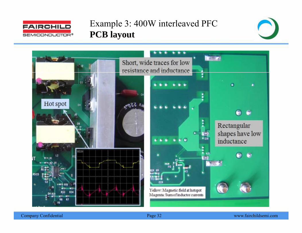
Example 3: 400W interleaved PFCPCB layout
www.fairchildsemi.comCompany Confidential Page 32
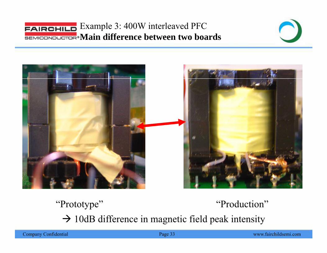
Example 3: 400W interleaved PFCMain difference between two boards
“Prototype” “Production”
www.fairchildsemi.comCompany Confidential Page 33
Prototype Production10dB difference in magnetic field peak intensity
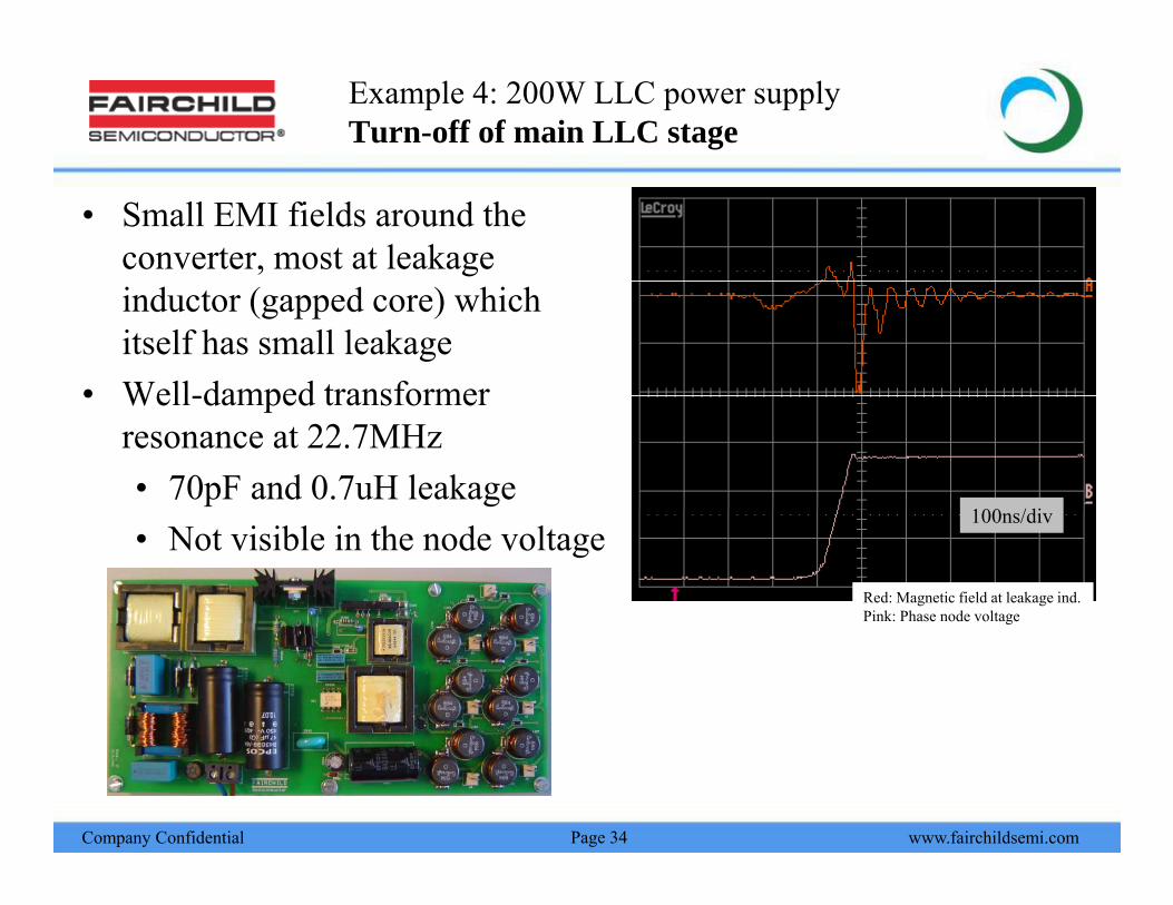
Example 4: 200W LLC power supplyTurn-off of main LLC stage
• Small EMI fields around the converter, most at leakage inductor (gapped core) which itself has small leakage
• Well damped transformer• Well-damped transformer resonance at 22.7MHz• 70pF and 0.7uH leakage
100 /di• Not visible in the node voltage
100ns/div
Red: Magnetic field at leakage ind.Pink: Phase node voltageg
www.fairchildsemi.comCompany Confidential Page 34
Agenda
• Introduction• Different types of EMI and their characteristicsDifferent types of EMI and their characteristics• Regulations and standards for EMI• Measurement and sources of EMI
• Conducted EMI• Radiated EMI
• EMI as integral part of the design flow• Conclusion
www.fairchildsemi.comCompany Confidential Page 35
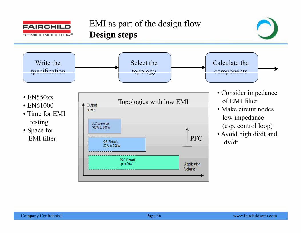
EMI as part of the design flowDesign steps
Write thespecification
Select thetopology
Calculate thecomponentsspecification topology
• EN550xx
components
Topologies with low EMI• Consider impedance
of EMI filter• EN61000• Time for EMI
testing• Space for
Topologies with low EMI of EMI filter• Make circuit nodes
low impedance(esp. control loop)
Space for EMI filter
• Avoid high di/dt anddv/dtPFC
www.fairchildsemi.comCompany Confidential Page 36
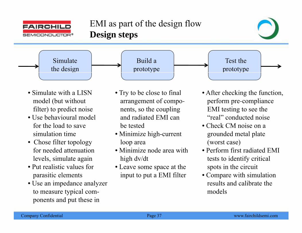
EMI as part of the design flowDesign steps
Simulatethe design
Build aprototype
Test theprototypeg p yp p yp
• Simulate with a LISN model (but without
• Try to be close to finalarrangement of compo-
• After checking the function,perform pre-compliancemodel (but without
filter) to predict noise• Use behavioural model
for the load to save
arrangement of components, so the couplingand radiated EMI canbe tested
perform pre complianceEMI testing to see the“real” conducted noise
• Check CM noise on a simulation time
• Chose filter topologyfor needed attenuationlevels, simulate again
• Minimize high-currentloop area
• Minimize node area withhigh dv/dt
grounded metal plate (worst case)
• Perform first radiated EMItests to identify criticallevels, simulate again
• Put realistic values forparasitic elements
• Use an impedance analyzert t i l
high dv/dt• Leave some space at the
input to put a EMI filter
tests to identify criticalspots in the circuit
• Compare with simulationresults and calibrate the
d l
www.fairchildsemi.comCompany Confidential
to measure typical com-ponents and put these in
models
Page 37

EMI as part of the design flowDesign steps
Add theEMI filter
Design thefinal version
Test thefinal version
• Build the EMI filter intothe prototype and perform
• Final implementation willchange the noise “signature”
• After full functional testing,perform pre-compliancep yp p
full functional test again• Check if EMI filter impe-
dance and possible reso-nances create any issues
g gof conducted DM and CMas well as radiated EMI
• (Alternate source) compo-nents used in production
p p ptesting especially and highand low line conditionsover full load range
• Try out different passivenances create any issues• Perform pre-compliance
testing again to see if the measured attenuation
nents used in production may have different para-sitics, so the EMI behaviour may change – need to add
• Try out different passive components (including different vendors)
• Build several prototypesmatches calculation appropriate margins and check if the noise results
are repeatable
www.fairchildsemi.comCompany Confidential Page 38
Agenda
• Introduction• Different types of EMI and their characteristicsDifferent types of EMI and their characteristics• Regulations and standards for EMI• Measurement and sources of EMI
• Conducted EMI• Radiated EMI
• EMI as integral part of the design flow• Conclusion
www.fairchildsemi.comCompany Confidential Page 39

Conclusion
• There is no silver bullet!• Switching currents and voltages will generate EMISwitching currents and voltages will generate EMI
• Assess implications early in the design cycle, and prepare• The later in the design cycle the problem is detected, the more g y p
expensive it is to fix• Use topologies and control ICs that create less noise to begin with
C Q fl b k S• LLC, QR flyback, PSR
References:References:[1] Didier Bozec, David Cullen, Les McCormack, John Dawson, Bryan Flynn: An investigation into the EMC emissions from switched
mode power supplies and similar switched electronic load controllers operating at various loading conditions (IEEE Symposium on Electromagnetic Compatibility, Santa Clara CA, August 2004)
[2] Bruce Carsten: Application note for H-field probe (http://bcarsten.com)
www.fairchildsemi.comCompany Confidential
[3] Jonathan Harper: Electromagnetic compatibility design for power supplies (Fairchild Semiconductor power seminar series 2004/2005)[4] Richard Lee Ozenbaugh: EMI filter design (CRC, Nov 2000)[5] Christophe Basso: Switch-Mode Power Supplies SPICE Simulations and Practical Designs“, McGraw-Hill, 2008
Page 40

Follo s on T itter @ http://t itter com/fairchildSemiFollow us on Twitter @ http://twitter.com/fairchildSemi
View product and company videos @ http://www.fairchildsemi.com/video/index.html
Listen to our podcasts @ http://www.fairchildsemi.com/company/media_center/index.html
Comment on our blog @ http://engineeringconnections.com/blog/
www.fairchildsemi.comCompany Confidential Page 41