Embed Size (px)
Citation preview
366 Wireless World, August 1973
Electronic Sound Synthesizer First of three articles describing the operation and construction of a modular system with manual or electromc voltage control of synthesized wavefonns
by T. Orr* tB.Se. and D. W. Thomast Ph.D., l�I.I.E.R.E.
The electronic sound synthesizer is an instrument that can generate a variety of complex outputs, the parameters of which are variable and are' controlled by the device itself. In its most common form, the synthesizer is used as an electronic musical instrument, usually being a monophonic keyboard device. It is also to be found in more fixed purpose applications, such as animal "alarm call" generators.
Basically, the synthesizer is capable of generating and processing signals, and by employing such techniques as frequency and amplitude modulation, filtering and mixing, it is usually possible to produce a desirable output. The feature that makes the synthesizer unique from other instruments, such as organs or electric pianos, is its voltage control capability. This enables parameters such as frequency, amplitude, modulation, attack and reverberation, to be not only manually con trolled, but also electronically controlled. Couple this voltage control capability to a flexible programming unit and the result is an instrument with an enormous range of possible tone colours. The versatility of the synthesizer can be further extended by the inclusion of more and more functional units, but this approach is over-sophisticated. It is better to try to analyse just what is required and how best to achieve it. For instance, what particular types of sounds should the synthesizer generate; is it for instance, going to be used as a piece of educational equipment or for quantitatively synthesizing known waveforms, for example bird calls, engine noises, spoken words etc? This is the "deep end" of synthesizer technology where a great deal of effort has been expended for few returns. Where reasonable returns have been achieved it has been, generally, with computer backup.
Sound synthesis As a musical instrument the synthesizer is well cast. The world of qualitative descriptions is an ideal environment for a machine that continually defies a quantitative approach. The synthesizer is often used to generate special effects and
t University of Southampton . • Now with Electronic Music Studios Ltd.
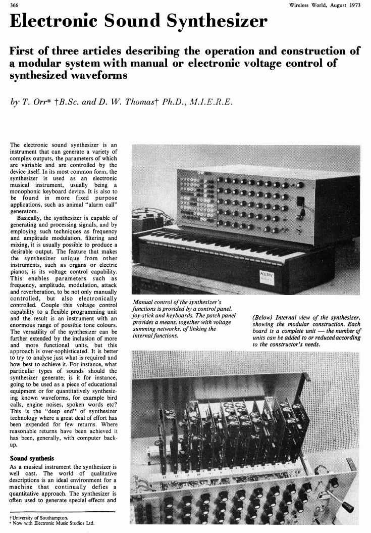
Manual control of the synthesizer's functions is provided by a control panel,
joy-stick and keyboards. The patch panel provides a means, together with voltage summing networks. of linking the internal functions.
(Below) Internal view of the synthesizer, showing the modular construction. Each board is a complete unit - the number of units can be added to or reduced according to the constructor's needs.
Wireless World, August 1973
CD voltage c.ontrolled
Units
audio mixer
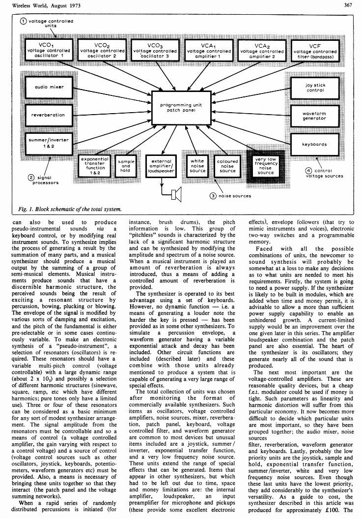
Fig. 1. Block schematic of the total system.
can also be used to produce pseudo-instrumental sounds via a keyboard control, or by modifying real instrument sounds. To synthesize implies the process of generating a result by the summation of many parts, and a musical synthesizer should produce a musical output by the summing of a group of semi-musical elements. Musical instruments produce sounds that have a discernible har monic structure, the perceived sounds being the result of exciting a resonant structure by percussion, bowing, plucking or blowing. The envelope of the signal is modified by various sorts of damping and excitation, and the pitch of the fundamental is either pre-selectable or in some cases continuously variable. To make an electronic synthesis of a "pseudo-instrument", a selection of resonators (oscillators) is required. These resonators should have a variable multi-pitch control (voltage controllabie) with a large dynamic range (about 2 x 1°3) and possibly a selection of different harmonic structures (sinewave, square, ramp, etc which have different harmonics; pure tones only have a limited use). Three or four of these resonators can be considered as a basic minimum for any sort of modest synthesizer arrangement. The signal amplitude from the resonators must be controllable and so a means of control (a voltage controlled amplifier, the gain varying with respect to a control voltage) and a source of control (voltage control sources such as other oscillators, joystick, keyboards, potentiometers, waveform generators etc) must be provided. Also, a means is necessary of bringing these units together so that they interact (the patch panel and the voltage summing networks).
When a rapid series of randomly distributed percussions is initiated (for
instance, brush drums), the pitch information is low. This group of "pitchless" sounds is characterized by the lack of a significant harmonic structure and can be synthesized by modifying the amplitude and spectrum of a noise source. When a musical instrument is played an am ount of reverberation is always introduced, thus a means of adding a controlled amount of reverberation is provided.
The synthesizer is operated to its best advantage using a set of keyboards. However, no dynamic function - i.e. a means of generating a louder note the harder the key is pressed - has been provided as in some other synthesizers. To simulate a percussion envelope, a waveform generator having a variable exponential attack and decay has been included. Other circuit functions are included (described later) and these corn bine with those units already mentioned to produce a system that is capable of generating a very large range of special effects.
The total collection of units was chosen after monitoring the format of commercially available synthesizers. Such items as oscillators, voltage controlled amplifiers, noise sources, mixer, reverberation, patch panel, keyboard, voltage controlled filter, and waveform generator are common to most devices but unusual items included are a joystick, summer / inverter, exponential transfer function, and a very low frequency noise source. These units extend the range of special effects that can be generated. Items that appear in other synthesizers, but which had to be left out due to time, space and money limitations are: the internal amplifier, loudspeaker, an input preamplifier for microphone and pickups (these provide some excellent electronic
VCF voltage controlled
filter (band pass)
joy stick control
367
effects), envelope followers (that try to mimic instruments and voices), electronic two-way switches and a programmable memory.
Faced with all the possible combinations of units, the newcomer to sound synthesis will probably be somewhat at a loss to make any decisions as to what units are needed to meet his requirements. Firstly, the system is going to need a power supply. If the synthesizer is likely to be built in modules, which are added when time and money permit, it is advisable to allow a more than sufficient power supply capability to enable an unhindered growth. A current-limited supply would be an improvement over the one given later in this series. The amplifier loudspeaker combination and the patch panel are also essential. The heart of the synthesizer is its oscillators; they generate nearly all of the sound that is produced.
The next most important are the voltage-controlled amplifiers. These are reasonable quality devices, but a cheap f.e.t. modulator could be used if money is tight. Such parameters as linearity and harmonic distortion will suffer from this particular economy. It now becomes more difficult to decide which particular units are most important, so they have been grouped together; the audio mixer, noise sourc.es (coloured), voltage controlled filter, reverberation, waveform generator and keyboards. Lastly, probably the low priority units are the joystick, sample and hold, exponential transfer function, summer /inverter, white and very low frequency noise sources. Even though these last units have the lowest priority, they add considerably to the synthesizer'S versatility. As a guide to cost, the synthesizer described in this article was produc�d for approximately £ 100. The
368 performance of the machine, as with other synthesizers, is not sufficient for it to be a main instrument for live 'performances, due mainly to speed considerations in setting up patches and pots. The only way to obtain a versatile performance entirely from the synthesizer is to use multi-track recording techniques. The system The synthesizer may be considered as a series of separate units, each with their own respective sub-groupings (see Fig. 1).
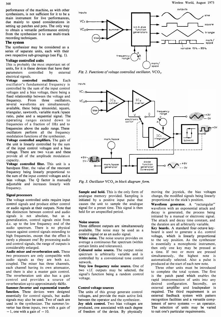
Voltage controlled units This is probably the most important set of units, for it is these devices that have their parameters controlled by external electrical signals. Voltage controlled oscillators. Each osci llator's fundamental frequency is controlled by the sum of the input control volt ages and a bias voltage, there being a fixed relationship between the voltage and frequency. From three oscillators, several waveforms are simultaneously available, these being sinusoidal, square, triangular, sawtooth, variable mark /space ratio, pulse and a sequential signal. The operating ranges extend down to frequencies of a fraction of I Hz and to frequencies above the audio range. These oscillators perform all the frequency modulation functions of the synthesizer. Voltage controlled amplifiers. The gain of the unit is linearly controlled by the sum of the input control volt ages and a bias voltage. There are two v.c.as and these provide all of the amplitude modulation capacity. Voltage controlled filter. This unit is a bandpass filter, the value of the resonant frequency being linearly proportional to the sum of the input control volt ages and a bias voltage. The Q factor is manually adjustable and increases linearly with frequency.
Signal processors
The voltage controlled units require input control signals and produce either control or audio signals at their outputs. Note that the distinction between control and audio signals is not absolute, but as a generalization, control signals exist from d.c. up to the low frequency end of the audio spectrum. There is no physical reason against control signals extending to high frequencies, except that the effect is rarely a pleasant one! By processing audio and control signals, the range of outputs is considerably enlarged. Audio mixer and reverberation unit. These two processors are only compatible with audio signals as they are both a.c. coupled. The mixer has three channels, each channe1 having its own attenuator, and there is also a master gain control. The reverberation unit also has a gain control and provides a source of reverberation up to approximately 4kHz. Summer /inverter and exponential transfer function. These devices were designed essentially for control signals, but audio signals may also be used. Two of each are used in the synthesizer. The summer /invert er has three inputs, two with a gain of -I, one with a gain of - 10.
Inputs
frequency range
II.C.O. �Ius function
generators
mark/ space
Wireless World, August 1973 outputs � slne
squ are-
� triangle
::nm-l ry-n .... -_--_-'.&., __ �pc:,r::
variable 15'10 - 85°,.
Fig. 2. Functions q(voltaf(e controlled oscillator, VCOI.
inputs
vc,o-__ � __ ��
VC 2 o---... -t
(� I I
frequency range
C
mark/.pace i ff I I Schmitt I I I I L. _______________________ ...1
mark/space generator
diode function
generator (sinewave)'
"- �-+6V V . --QV
Fig. 3. Oscillator VCO 1 in block diagram form.
Sample and hold. This is the only form of analogue memory provided. Sampling is initiated by a positive input pulse that causes the unit to sample the analogue signal for a preset time. This signal is then held for an unspecified period.
Noise sources Three different outputs are simultaneously available. The noise may be used as a control signal or as an audio signal. Wbite noise. The noise source provides on average a continuous flat spectrum (within certain limits and tolerances). Coloured noise source. The output noise spectrum is arbitrarily variable and is controlled by a conventional tone control network. Very low frequency noise source. One of two v.l.f. outputs may be selected, the signal's function being a random control voltage.
Control voltage sources The units of this group generate control voltages, and provide the main active link between the operator and the synthesizer. Joy stick control. Two bias voltages are produced, one associated with each degree of freedom of the device. By physically
moving the joystick, the bias voltages change, the modified signals being linearly proportional to the stick's position. Waveform generator. A "rectangular" waveform with an exponential attack and decay is generated, the process being initiated by a manual or electronic signal. The attack and decay time constant, and the duration are all arbitrarily variable. Key boards. A standard four- octave keyboard is used to generate a d.c. control voltage, which is linearly proportional to the key position. As the synthesizer is essentially a monophonic instrument, then only one key may be pressed at a time. If two or more are pressed simultaneously, the highest note is automatically selected. Also a pulse is produced at the start of each new note.
Three other units must be introduced to complete the total system. The first is the patch panel which enables the rapid interconnection of units into any desired configuration. Secondly, an external amplifier and loudspeaker is required. The third requirement is an external feedback system with pattern recognition facilities and a versatile complement of servo systems - an operator. The selection of units may be varied to suit one's particular requirements.

Wireless World, August 1973
+Vcc
Rl 10k
FREQUENCY RANGE
+5V
01 lN914
O2 lN914
-Vcc
R5 lk
R9 lk
Rll 5Rl
L-______ -, triangular wave output
R29��� ______ -, lk
R3 0 >� __
____ � lk
V C 1
+Vcc
Cll 25}"
/25V
R3 1 R32 1k 50k MIN.
BIAS FREQUENCY
06 lN914
05 1N914 R2 2
* 3k 3
"--�--"------"--------"------------------------"- OV
Fig. 4. Circuit of VCOI• All resistors are 5%, 1 W unless asterisked - these are 2%.
Design in general
There are certain rules that have to be enforced if the synthesizer is to work satisfactorily. Firstly, it is essential to generate and measure all signals relative to �V, and this requires a reliable grounding system. A stack of star terminals was employed for this, to which were connected the ground wires from the control pots and all the OV supply lines from the edge connectors.
A signal level of 3V was selected, this giving ample room for larger signal excursions. Also as there is a considerable amount of wiring between the pots, circuits and patch panel, the input and output impedance of the units was kept low so that un screened wiring could be used without any serious interference or crosstalk problems occurring. The input impedances are typically lkD and the output impedances must be correspondingly lower to avoid loading. Some control signals are low frequency or even direct voltages and so a.c. coupling between units is not a practical proposition (with the exception of the audio mixer and the reverberation unit). The most significant problem with direct coupling is the fact that control signals
are never what they ought to be, but always have an offset voltage added to them. Most of these offset voJtages are only a few hundred milIivolts (positive), but this is enough to cause disturbing effects. However, the variable bias on the voltage controlled units should be capable of overcoming most offsets.
The general layout of the synthesizer can be seen in the photograph. Most of the circuitry was constructed on plug-in boards and although the connectors increase the cost, they do provide the advantage of making the boards removeable for servicing. Also a spacious layout has been used, enabling clear access to the control pots. Even with a stabilized supply and a reasonable ground system it may prove necessary to decouple the power supply on each board. Minor transients of the supply levels can be disturbing as they can build up into a noticeable background noise, and may even cause the v.c.os to lock on to each other's harmonics.
The synthesizer bears a strong resemblance to an analogue computer, with an array of control pots to vary parameters, a patching system and a selection of functional electronic units. However,
Ca 4n7
+Vcc +15V
R17
Tr5 BC213L
square wave output
a
-Vs
2k2 Tr7
BCla2L
1 14
369
-Vcc
-15V
In\/.I/p 741 +Vs 4G] 1
G8 non In\/, DIP. output
IIp in\/.. i/P 8-p·,n +Vs -v,
non in\/. D.I.L. t t 7 8 ijp ou pu 4 5
TOP VIEW
whereas the analogue computer makes an attempt at being quantitative and accurate, this synthesizer does not, relying strongly on the qualitative perception of the operator
First voltage controlled oscillator
This oscillatorZ has a linear frequency/ voltage characteristic and produces four outputs as shown in Fig. 2. These are square, triangular, sinusoidal and a variable mark/space ratio rectangular waveform. The oscillator has three frequency ranges, the top range covering the audio spectrum, the bottom two extending to subsonic frequencies. The quiescent operating point may be shifted by altering the bias level, and the input control voltages (VC" VCz) may be attenuated by control pots. The final operating frequency is linearly proportional to the sum of the bias voltage and the attenuated control voltages, and should have a dynamic range of at least three decades.
The heart of the oscillator is a trianglesquarewave generator (Fig. 3) where a Schmitt trigger provides positive feedback around an integrator; the integrator's output thus ramps up and down inside
370 the hysteresis window of the Schmitt trigger. The oscillator is both self-starting and stable, having a large dynamic operating range and a defined amplitude. Two outputs are produced, a triangle at the integrator's output and a square wave from the Schmitt trigger. The ramp rate, and hence the operating frequency, may be varied by altering either the integrator's gain and/or the drive voltage.
The two voltages V and V (Fig. 3) are alternately switched into the integrator .by the electronic switch (a diode ring switch D7, 8' 9' 10' Fig 4), which is controlled by the Schrnitt trigger. The voltage V is produced at the output of le3, where the output is depressed by the forward drop across diode D6• Ideally D6-lo should all be matched and so should resistors R21, 24' 36' and R22, 23' thus preserving as far as possible the linear voltage/frequency characteristic and signal symmetry. However, as matched diodes are relatively expensive, it was decided to use unmatched unselected diodes.
This had the effect of causing some nonIinearities which were only noticeable at low frequencies where the diodes were conducting very low currents. To obtain the required gain from le3, resistor R36 had to be much larger than Rw 24' and this resulted in a loss of voltage/ frequency linearity at low frequencies. This effect is not very noticeable, but imbalance in the ring switch may cause a disturbing loss of symmetry (Fig. 7). This can be nulled by preset R2 (Fig. 4) which is set to cancel the offset caused by the ring switch's imbalance at its minimum operating point. To preserve as much symmetry as possible, R21-24 are all 2% tolerance resistors.
Diode D3 (Fig. 4) is included to protect Tr I' Tr 2' against emitter-base breakdown; if for any reason the feedback loop is broken, the output of lel may ramp down unhindered, with irreversible results. The Schrnitt trigger used is the SN7413N, a t.t.1. integrated circuit. The whole of the circuit operation relies upon the stability of the hysteresis levels; if they alter, then the amplitude and frequency of the output will change. Thus it is particularly essential to have a stabilized and decoupled 5V supply for le2 as well as for Vcc- If this is not achieved then spikes on the power supplies will cause oscillators veal and veo2 to have a tendency to lock onto one another's harmonics. To reduce the generation of spikes, the output of the Schmitt trigger is capacitively loaded; this however, has little effect on the square wave production at audio frequencies.
It should be pointed out that using the SN7413N for the Schmitt trigger has its drawbacks. The separation between its hysteresis levels is small, making it vulnerable to interference by other v.c.os. Its fast rise and fall times can generate significant interference and also it does not like driving long lengths of cable. These difficulties have been largely overcome, but a Schmitt trigger of discrete components would still be an improve-
+15V
D2 - D11 1N914
Wireless World, August 1973
sinewave output
ov J\.f\.,
R9 1k5
i n pu t . A A output of integrator / V V (IC1.Fig.4)
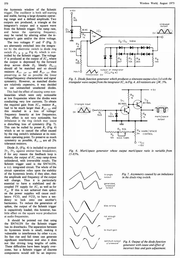
ov Fig. 5. Diode function generator which produces a sinewave outpui whenfcd with the triangular wave output from the integrator lel in Fig. 4. A II resistors are + W. 5%.
triangle inp�t
OV ./\/'v R1 5k6 D1
1N914
+5V
Tr2 BCIB2L
t---- lfLr mark! space
output
R3 50k ��VV����--� R4 MARK / SPACE 5k CONTROL
-VCC -15V
Fig. 6. Mark/space generator whose output mark/space ratio is variable from 15-85%.
vv vv vv vv
triangle output
generated 'sinewave'
output
bids wrong
not enough gain
to much gain
optimum output o 'sinewave t
Fig. 7. Asymmetry caused by an imbalance in the diode ring switch.
Fig. 8. Output of the diode function generator with cause and effect of incorrect bias and gain adjustment.
Wireless World, August 1973
VC, 0----+-1""" v.c.o. plus function
generators
fre'l.uency range
outputs � sine
� square
� triangle
ramp
n n mark! -----.J L----...J L-- space
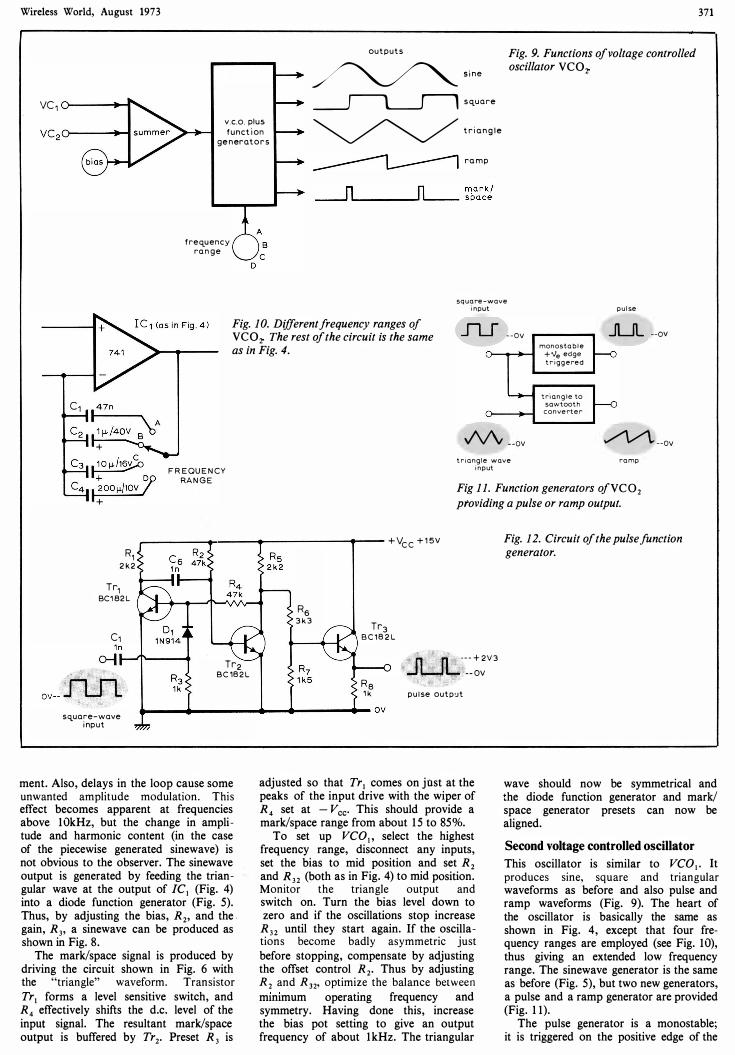
Fig. 9. Functions o/ voltage controlled oscillator yeo?
371
square-wave input pulse
C,
Fig. 10. DifJerent /requency ranges 0/ yeo? The rest o/ the circuit is the same as in Fig. 4.
--OV
�
JLJL --QV monostable
+Ve edge j---o triggered
triangle to
j---o sawtooth converter
� --QV ,../'\./\. --QV
FREQUENCY RANGE
triangle wave input
ramp
Fig 11. Function generators 0/ye02 providing a pulse or ramp output.
�----_---�-----�p-- +Vcc +'5V Fig. 12. Circuit o/ the pulse /unction generator. R1
2k2
Tr, BC'B2L
C, o-Il---'1'---i
QV-- JLf1. Tr2
BC182L
R6 3k3
Tr3 BC'82L
R8 'k
" .. n. ,.---+2V3 ..J I,......J L.... --QV pulse outP'Jt
s�uare-wave input
.. ____ .. __________ �--4-------��QV
ment. Also, delays in the loop cause some unwanted amplitude modulation. This effect becomes apparent at frequencies above 10kHz, but the change in amplitude and harmonic content (in the case of the piecewise generated sinewave) is not obvious to the observer. The sinewave output is generated by feeding the triangular wave at the output of ICI (Fig. 4) into a diode function generator (Fig. 5). Thus, by adjusting the bias, R2, and the. gain, R3, a sinewave can be produced as shown in Fig. 8.
The mark/space signal is produced by driving the circuit shown in Fig. 6 with the "triangle" waveform. Transistor Trl forms a level sensitive switch, and R4 effectively shifts the d.c. level of the input signal. The resultant mark/space output is buffered by Tr2• Preset R3 is
adjusted so that Trl comes on jost at the peaks of the input drive with the wiper of R4 set at - VCC. This should provide a mark/space range from about 15 to 85%.
To set up VCOI' select the highest frequency range, disconnect any inputs, set the bias to mid position and set R 2 and R32 (both as in Fig. 4) to mid position. Monitor the triangle output and switch on. Turn the bias level down to zero and if the oscillations stop increase
R 32 until they start again. If the oscillations become badly asymmetric just before stopping, compensate by adjusting the offset control R2• Thus by adjusting R2 and R32, optimize the balance between minimum operating frequency and symmetry. Having done this, increase the bias pot setting to give an output frequency of about 1kHz. The triangular
wave should now be symmetrical and the diode function generator and mark/ space generator presets can now be aligned.
Second voltage controlled oscillator
This oscillator is similar to VCO I. It produces sine, square and triangular waveforms as before and also pulse and ramp waveforms (Fig. 9). The heart of the oscillator is basically the same as shown in Fig. 4, except that four frequency ranges are employed (see Fig. 10), thus giving an extended low frequency range. The sinewave generator is the same as before (Fig. 5), but two new generators, a pulse and a ramp generator are provided (Fig. 11).
The pulse generator is a monostable; it is triggered on the positive edge of the
372
square-wave output and produces a pulse of approximately 20f-ls duration (Fig. 12).
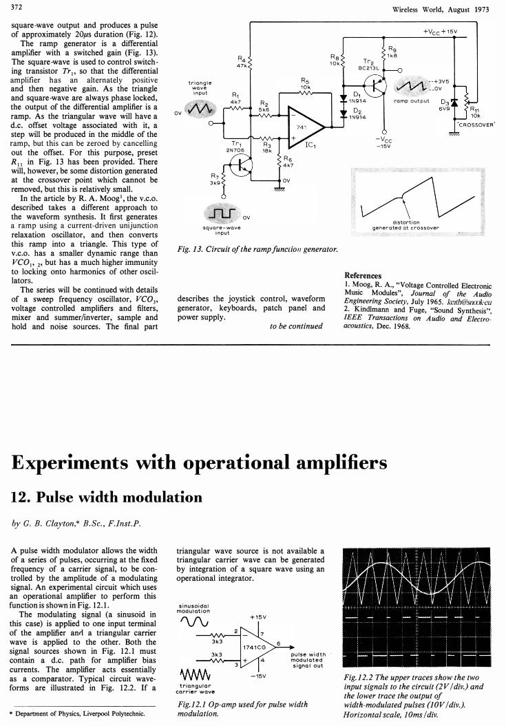
The ramp generator is a differential amplifier with a switched gain (Fig. 13). The square-wave is used to control switching transistor Tr 1> so that the differential amplifier has an alternately positive and then negative gain. As the triangle and square-wave are always phase locked, the output of the differential amplifier is a ramp. As the triangular wave will have a d.c. offset voltage associated with it, a step will be produced in the middle of the ramp, but this can be zeroed by cancelling out the offset. For this purpose, preset R 11 in Fig. 13 has been provided. There will, however, be some distortion generated at the crossover point which cannot be removed, but this is relatively small.
In the article by R. A. Moogl, the v.c.o. described takes a different approach to the waveform synthesis. It first generates a ramp using a current-driven unijunct
'ion
relaxation oscillator, and then converts this ramp into a triangle. This type of v.c.o. has a smaller dynamic range than VCOI, 2' but has a much higher immunity to locking onto harmonics of other oscillators.
The series will be continued with details of a sweep frequency oscillator, VC03, voltage controlled amplifiers and filters, mixer and summer/inverter, sample and hold and noise sources. The final part
OV
R4 47k
triangle wave input R1
.(\1\ 4k7
Tr1 2N706
R7 3k9
square-wave input
R2 5k6
R3 18k R6 4k7
OV
R8 10k
Fig. 13. Circuit of the ramp function generator.
describes the joystick control, waveform generator, keyboards, patch panel and power supply.
to be continued
Wireless World, August 1973
+VCC+15V
Rg 1k8
Tr2 BC213L
-VCC -15V
.A A --+3V5 v V "' __ �V
ramp output
distortion generated at cro ssover
References I. Moog, R. A., "Voltage Controlled Electronic Music Modules", Journal of the Audio Engineering Society, July 1965. kelm@Snrokeu 2. Kindlmann and Fuge, "Sound Synthesis", IEEE Transactions on Audio and Electroacoustics, Dec. 1968.
Experiments with operational amplifiers
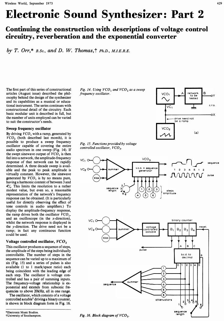
12. Pulse width modulation by C. B. Clayton,* B.Sc., F.Inst.P.
A pulse width modulator allows the width of a series of pulses, occurring at the fixed frequency of a carrier signal, to be controlled by the amplitude of a modulating signal. An experimental circuit which uses an operational amplifier to perform this function is shown in Fig. 12.1.
The modulating signal (a sinusoid in this case) is applied to one input terminal of the amplifier ann a triangular carrier wave is applied to the other. Both the signal sources shown in Fig. 12.1 must contain a d.c. path for amplifier bias currents. The amplifier acts essentially as a comparator. Typical circuit waveforms are illustrated in Fig. 12.2. If a
* Department of Physics, Liverpool Polytechnic.
triangular wave source is not available a triangular carrier wave can be generated by integration of a square wave using an operational integrator.
sinusoidal modulation
3k3 3k3
triangular carrier WQve
2
3
+15 V
-15V
pulse width modulated signal out
Fig.12.1 Op-amp used for pulse width modulation.
Fig.12.2 The upper traces show the two input signals to the circuit (2 V / div.) and the lower trace the output of width-modulated pulses (JOV /div.). Horizontal scale, 10ms /div.
Wireless World, September 1973
Electronic Sound Synthesizer: Part 2 Continuing the construction with descriptions of voltage control circuitry, reverberation and the exponential converter
by T. Orr,* B.Sc., and D. W. Thomas,t Ph.D., M.f.E.R.E.
The first part of this series of constructional articles (August issue) described the philosophy behind the design of the synthesizer and its capabilities as a musical or educational instrument. The series continues with constructional detail of the circuitry. Each basic modular unit is described in full, but the number of units employed can be varied to suit the constructor's needs.
Fig. 14. Using Veal and veo2 as a sweep frequency oscillator. VCO, � rv
network � to be tested
Sweep frequency oscillator
Fig. 15. Functions provided by voltage controlled oscillator, veo3.
VC, � C.r.
...-- drive need not be a ramp
VC02
v"'V\, Ca)
429
y
o.
x
By driving veal with a ramp, generated by veol (both described last month), it is possible to produce a sweep frequency oscillator capable of covering the entire audio spectrum in one sweep (Fig. 14). If the swept sinewave output of Veal is then fed into a network, the amplitude-frequency response of that network can be rapidly determined. A three decade sweep is available and the peak to peak amplitude is virtually constant. However, the sinewave generated by Veal is by no means pure, having a harmonic content of between 3 and 4%. This limits the resolution to a rather modest value, but even so, a reasonable representation of the network's frequency response can be obtained. (It is particularly useful for directly observing the effect of tone controls in audio amplifiers.) To display the amplitude-frequency response, the ramp drives both the oscillator Veal' and an oscilloscope (in the x-direction), whilst the network response is displayed in the y-direction. The drive need not be a ramp; in fact any continuous function could be used.
VC, � sequence
Voltage controlled oscillator, VC03
This oscillator produces a sequence of steps, the amplitude of the steps being individually controllable. The number of steps in the sequence can be varied up to a maximum of six (Fig. 15) and a series of pulses is also available (1 to 1 mark/space ratio) each being coincident with the leading edge of each step. The oscillator is voltage controlled and has a pair of summing inputs. The frequency-voltage relationship is exponential and extends from subsonic frequencies to above 20kHz, all in one range.
The oscillator, which consists of a voltage controlled astable1 driving a binary counter, is shown in block diagram form in Fig. 16.
"Electronic Music Studios. tUniversity of Southampton.
VC,
sequence length
seq,uence
Fig. 16. Block diagram of veo3.
v.c.o. + sequence generator
voltage controlled
astable
pulse
2 3 4 5 ' 2
JlIl..JlJl..f1. pulse
binary counter
A B C
b.c.d. to 6 decimal
attenuators 2 3 4 5
seq,uence length
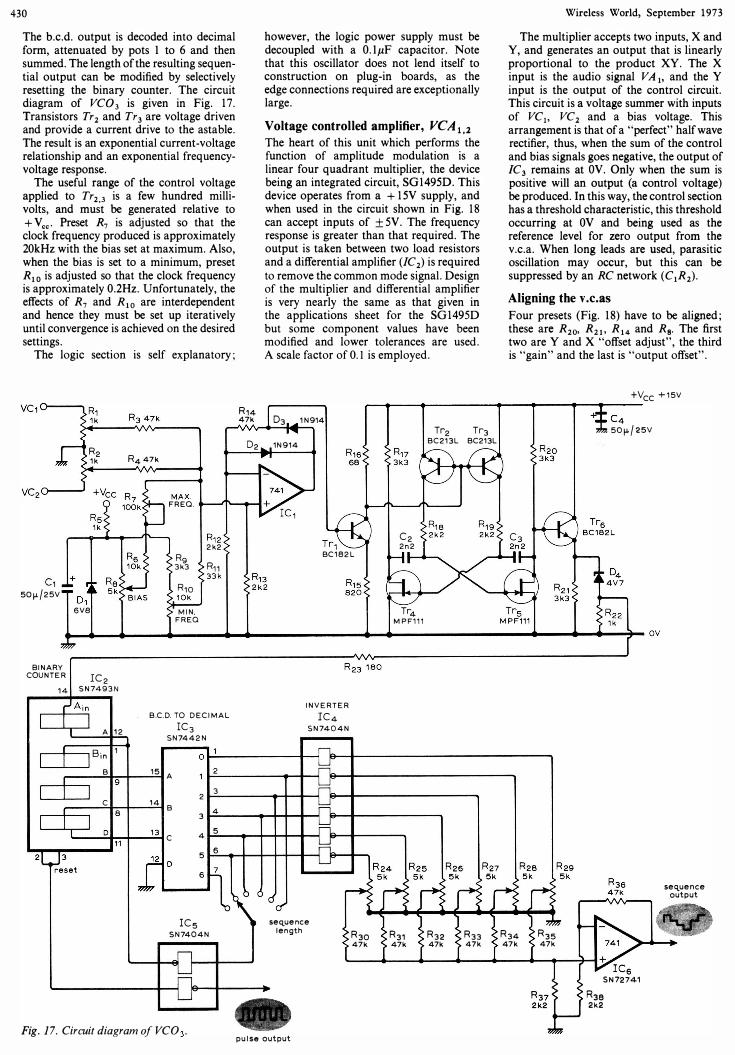
430 The b.c.d. output is decoded into decimal form, attenuated by pots I to 6 and then summed. The length of the resulting sequential output can be modified by selectively resetting the binary counter. The circuit diagram of VC03 is given in Fig. 17. Transistors Tr2 and Tr3 are voltage driven and provide a current drive to the astable. The result is an exponential current-voltage relationship and an exponential frequencyvoltage response.
The useful range of the control voltage applied to Tr2•3 is a few hundred millivolts, and must be generated relative to + Vcc' Preset R7 is adjusted so that the clock frequency produced is approximately 20kHz with the bias set at maximum. Also, when the bias is set to a minimum, preset RIo is adjusted so that the clock frequency is approximately 0.2Hz. Unfortunately, the effects of R7 and RI O are interdependent and hence they must be set up iteratively until convergence is achieved on the desired settings.
The logic section is self explanatory;
however, the logic power supply must be decoupled with a O.IJ.lF capacitor. Note that this oscillator does not lend itself to construction on plug-in boards, as the edge connections required are exceptionally large.
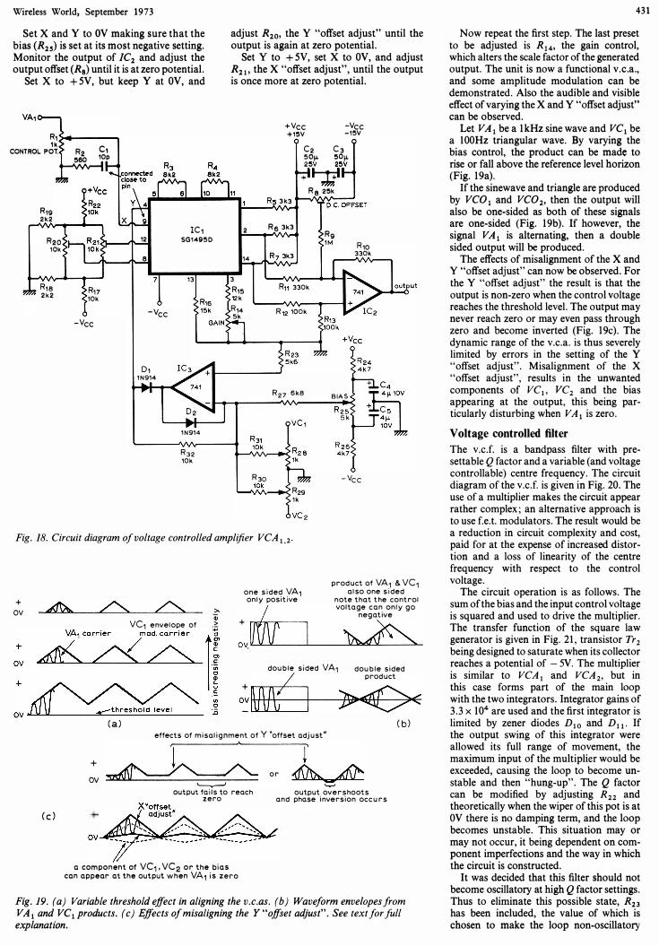
Voltage controlled amplifier, VCA1•2 The heart of this unit which performs the function of amplitude modulation is a linear four quadrant multiplier, the device being an integrated circuit, S01495D. This device operates from a + 15V supply, and when used in the circuit shown in Fig. 18 can accept inputs of ±5V. The frequency response is greater than that required. The output is taken between two load resistors and a differential amplifier (/C2) is required to remove the common mode signal. Design of the multiplier and differential amplifier is very nearly the same as that given in the applications sheet for the SO 1495D but some component values have been modified and lower tolerances are used. A scale factor of 0. 1 is employed.
Wireless World, September 1973 The multiplier accepts two inputs, X and
Y, and generates an output that is linearly proportional to the product XV. The X input is the audio signal V A I, and the Y input is the output of the control circuit. This circuit is a voltage summer with inputs of VCI, VC2 and a bias voltage. This arrangement is that of a "perfect" half wave rectifier, thus, when the sum of the control and bias signals goes negative, the output of IC3 remains at �V. Only when the sum is positive will an output (a control voltage) be produced. In this way, the control section has a threshold characteristic, this threshold occurring at OV and being used as the reference level for zero output from the v.c.a. When long leads are used, parasitic oscillation may occur, but this can be suppressed by an RC network (CIR2) .
Aligning the v.c.as
Four presets (Fig. 18) have to be aligned; these are R20, R21 , R I 4 and Re. The first two are Y and X "offset adjust", the third is "gain" and the last is "output offset".
R14 1 +VCC +15V ��---'---------'---4�--�--�----+l c4
15op./25v 47k D3 ..... 1N914 ?vv .....
r-1 D2 ... 1N914 � : �� R4 47k ...
VC2o------J�+-V.-C - C-R-7.1\1\Iv-- M- A-X- . -+ � � ��� 100ktJ FREO . .... r---Jn..� .......... � 1--' R1�<
C1.: �� 50p./25V .. D1U
6V8
2k2 R9 3k3 < R11
'l-33k R10
� MIN. FREO
T� BC182L
C2 2n2 · ...... u-·
Cll � Tr4
MPF111
Tr2 Tr3 BC213L BC213L
� J;)) c:V �
�� ____ � ____ � ______ ��� ______________ � __ �------------------�----4-__ �--�OV
BINARY COUNTER IC2
14 5N 7493N
r Ain
I I A 1 2
I I B. 1 In
B 9
I I C 8
I I
B.C.D. TO DECIMAL rC3 SN7442N
INVERTER 1C4 SN740 4N
""-""" 1 O�----------��
15 A 1�2� _____ �+-�
14 B 2 3
3 4 4 5 1..... __ D=+.� _.....;.:13'i C ... _ .... ----..... 11
2L�e�et
5 6
t"",,----,,' , 11 rC5 SN7404N
:, ( d seQ.uence
length
v v-
� >-�
seq.uence output
R30 > R31 R32 R33 > R3 4 R35 1 -_."-47k 'I- 47k 47k 47k < 47k .,. 47k 741 >-+--+
1.....---4----�----�--�----������ S N 72 741
R38 2k2
Fig. 17. Circuit diagram of VCO . pul se output
Wireless World, September 1973 Set X and Y to OV making sure that the
bias (Rl5) is set at its most negative setting. Monitor the output of [Cl and adjust the output offset (Rs) until it is at zero potential.
adjust Rlo, the Y "offset adjust" until the output is again at zero potential.
Set Y to + 5V, set X to �V, and adjust Rll, the X "offset adjust", until the output is once more at zero potential. Set X to +5V, but keep Y at �V, and
+Vcc -Vcc R, )0011------. +,�v -,�v 'k CONTROL POT.
R,g 2k2 R20 10k
R,e , 2k2
R C, 2 ,op �eo
R'7 10k
-Vcc
'2 e
-Vcc
D, lN914
lC, SG'49�D
13
R'6 15k
lN914
Rn 10k
C2 C3 �Oflo �Oflo
:�t-Jit Re 2�k R 3k3 -'"""""'o ..... c-. O-F-FSET
2
14
3 R,� 12k R'4 5k
Re 3k3
R" 330k
R'2 lOOk
Rg 11-1
R27 6kB BIAS
RIO 330k
R30 -Vcc _",'"O"k �P<.. R29 lk
Fig. 18. Circuit diagram of voltage controlled amplifier VCA 1.2'
+ ov '" Qj
one sided VA, only positive
+ rtr.i....-..---......,
product of VA, /I. VC, also one sided
note that the control vOltage can only go
negative VC, envelope of .�
:.�l! ov� ;
ov. "'-"'--'<-----1.----"-'''''''''--''----''''-
double sided VA, + / ov�1\ It I _ V V
double sided product
(cl
(a) effects of misalignment of Y 'offset adjust"
. +
or OV '------v--l
r 4\&. �
e output overshoots
X "Offset
output fails to reach zero and phase inversion occurs
. " , ,,' " . /' " L
+�"A� ov �� a component of VC,. VC2 or the bias can appear at the output when VA, is zero
(b)
Fig. 19. (a) Variable threshold effect in aligning the v.c.as. (b) Waveform envelopes from VAI and VCI products. (c) Effects of misaligning the Y "offset adjust". See text for full explanation.
431
Now repeat the first step. The last preset to be adjusted is R14, the gain control, which alters the scale factor of the generated output. The unit is now a functional v.c.a., and some amplitude modulation can be demonstrated. Also the audible and visible effect of varying the X and Y "offset adjust" can be observed.
Let VAI be a 1kHz sine wave and VCI be a 100Hz triangular wave. By varying the bias control, the product can be made to rise or fall above the reference level horizon (Fig. 19a).
If the sinewave and triangle are produced by VCOI and VCOl, then the output will also be one-sided as both of these signals are one-sided (Fig. 19b). If however, the signal VAI is alternating, then a double sided output will be produced.
The effects of misalignment of the X and Y "offset adjust" can now be observed. For the Y "offset adjust" the result is that the output is non-zero when the control voltage reaches the threshold level. The output may never reach zero or may even pass through zero and become inverted (Fig. 19c). The dynamic range of the v.c.a. is thus severely limited by errors in the setting of the Y "offset adjust". Misalignment of the X "offset adjust", results in the unwanted components of VCI, VCl and the bias appearing at the output, this being particularly disturbing when VAI is zero.
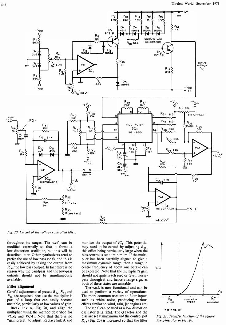
Voltage controlled filter
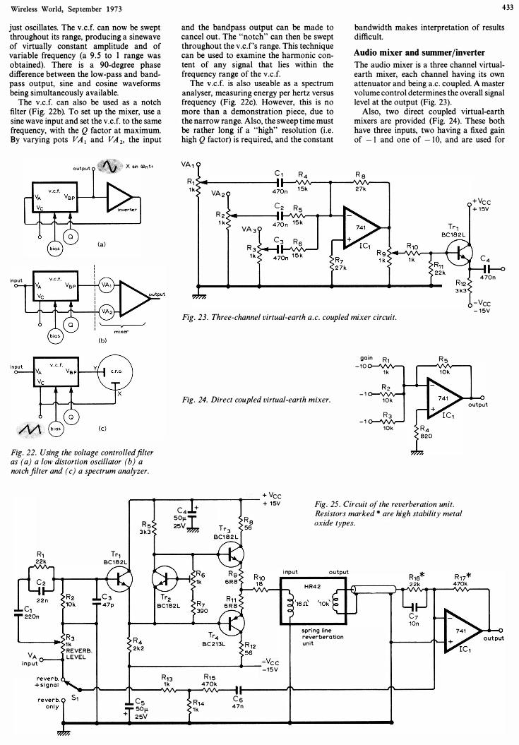
The v.c.f. is a bandpass filter with presettable Q factor and a variable (and voltage controllable) centre frequency. The circuit diagram of the v.c.f. is given in Fig. 20. The use of a multiplier makes the circuit appear rather complex; an alternative approach is to use f.e.t. modulators. The result would be a reduction in circuit complexity and cost, paid for at the expense of increased distortion and a loss of linearity of the centre frequency with respect to the control voltage.
The circuit operation is as follows. The sum of the bias and the input control voltage is squared and used to drive the multiplier. The transfer function of the square law generator is given in Fig. 21, transistor Trz being designed to saturate when its collector reaches a potential of - 5V. The multiplier is similar to VCAI and VCAl, but in this case forms part of the main loop with the two integrators. Integrator gains of 3.3 x 10⁴ are used and the first integrator is limited by zener diodes Dlo and Dll. If the output swing of this integrator were allowed its full range of movement, the maximum input of the multiplier would be exceeded, causing the loop to become unstable and then "hung-up". The Q factor can be modified by adjusting Rn and theoretically when the wiper of this pot is at OV there is no damping term, and the loop becomes unstable. This situation may or may not occur, it being dependent on component imperfections and the way in which the circuit is constructed.
It was decided that this filter should not become oscillatory at high Q factor settings. Thus to eliminate this possible state, Rn has been included, the value of which is chosen to make the loop non-oscillatory
432
input VA
+Vcc
DlO D11 4V5 4V5
-x
VBP output
Fig. 20. Circuit of the voltage controlledfilter.
throughout its ranges. The v.c.f. can be modified externally so that it forms a low distortion oscillator, but this will be described later. Other synthesizers tend to prefer the use of low pass v.c.fs, and this is easily achieved by taking the output from IC4, the low pass output. In fact there is no reason why the bandpass and the low-pass outputs should not be simultaneously available.
Filter alignment
Careful adjustments of presets R42, R44 and R3S are required, because the multiplier is part of a loop that can easily become unstable, particularly at low values of gain.
Break link A, Fig. 20, and align the multiplier using the method described for VCAI and VCA2. Note that there is no "gain preset" to adjust. Replace link A and
Wireless World, September 1973
.. ----�----.. ---1----�--.. ��OV
Re 10k
De D9 1N914 1N914
SQUARE LAW GENERATOR
Tr2 BC1B2L
control voltage Vc
-Vcc �------------------------�-----15V
+Vcc
9
4
12 e
-
link A
5
MULT I PL I ER 1C2
SG1495D
C5 251'-T+ 25V 0
+Vcc
3
monitor the output of lC,. This potential may need to be zeroed by adjusting R3" this offset being particularly large when the bias control is set at minimum. If the multiplier has been carefully aligned to give a maximum dynamic range, then a range in centre frequency of about one octave can be expected. Note that the multiplier's gain should not quite reach zero or (even worse) pass through it and hence change sign, as both of these states are unstable.
The v.c.f. is now functional and can be used to perform a variety of operations. The more common uses are to filter inputs such as white noise, producing various effects similar to wind, rain, jet engines etc.
4
+Vcc
R34 3k3 d.c. OFFSET
2 R33 3k3 R36 240k R29
14 R45 3K3 56k
R30 56k
+--OVLP
Vout
. Tr2 cut of! '" a. in lig. 22
iquarf' law region saturated The v.c.f. can be used as a low distortion
oscillator (Fig. 22a). The Q factor and the bias are set at maximum and the control pot R 18 (Fig. 20) is increased so that the filter
Fig. 21. Transfer function of the square law generator in Fig. 20.
Wireless World, September 1973
just oscillates. The v.c.r. can now be swept throughout its range, producing a sinewave of virtually constant amplitude and of variable frequency (a 9.5 to I range was obtained). There is a 9O-degree phase difference between the low-pass and bandpass output, sine and cosine waveforms being simultaneously available.
The v.c.f. can also be used as a notch filter (Fig. 22b). To set up the mixer, use a sine wave input and set the v.c.f. to the same frequency, with the Q factor at maximum. By varying pots V A 1 and V A 2, the input
v.c.f.
input
output t� X .in OOn t •
(a)
Fig. 22. Using the voltage controlledfilter as (a) a low distortion oscillator (b) a notch filter and (c) a spectrum analyzer .
and the band pass output can be made to cancel out . The "notch" can then be swept throughout the v.c.f 's range. This technique can be used to examine the harmonic content of any signal that lies within the frequency range of the v.c.r.
The v.c.r. is also useable as a spectrum analyser, measuring energy per hertz versus frequency (Fig. 22c). However, this is no more than a demonstration piece, due to the narrow range. Also, the sweep time must be rather long if a "high" resolution (i.e. high Q factor) is required, and the constant
VA , C 1 R1
R4 1 k
VA 2 1 Sk
R 2 R s
1 k 1 S k VA 3
R 3 R 6
1 k
433
bandwidth makes interpretation of results difficult.
Audio mixer and summer/inverter
The audio mixer is a three channel virtualearth mixer, each channel having its own attenuator and being a.c. coupled. A master volume control determines the overall signal level at the output (Fig. 23) .
Also, two direct coupled virtual-earth mixers are provided (Fig. 24) . These both have three inputs, two having a fixed gain of - I and one of - 1 0, and are used for
R a
27k
+ Vc c + 1 SV
C4 1---0
4 70n
- Vcc - 1 SV
Fig. 23. Three-channel virtual-earth a .c . coupled mixer circuit.
gain R1 R s - 1 0
1 k
R 2 - 1
Fig. 24. Direct coupled virtual-earth mixer. 1 0 k output R 3
- 1 10k
...---1----t-----...... -- + Vcc + 1 !5V Fig. 25. Circuit of the reverberation unit.
Resistors marked * are high stability metal oxide types.
R1 22k
... __ ---;� R3 1 k VA i nput
REVERB. LEVEL
51
Tr1 BC 1 a 2 L
C4 + SO�I 2SV ,
R a S6
t-_____________________ �---Vc c - 1 S V
C S SO� + 2SV
Rn R1 S 1 k 470k
C 6 47n
i nput output H R4 2
spring line reverberation un it
434
Tr3 B C 21 3 L
+ Vcc + 1 SV
Tr4 B C 1 B 2 L
o v
-Vcc - 1 SV
Fig. 26. Circuit of the exponential converter. Two converters are included in the synthesizer.
signal processing, such as inversion, summing or amplification.
Reverberation unit
The reverberation unit consists basically of three sections ; the driver, the springline reverberation unit and the equalised pickup amplifier (Fig. 25). The springline reverberation unit used was the "H242" obtainable from Henry's Radio . This unit is moderately inexpensive, but suffers from a loss of high frequency reverberation, dropping considerably at about 4kHz. However, a useful response can be obtained-enough in fact for this unit to be used in one of the commercially available synthesizers.
By operating switch S I ' a choice of the input signal plus reverberation, or just reverberation is available. Thus the reverberation can be separately controlled, by using a v.c.a. and/or a v.c.r. , as well as being manually controllable (R3)' To reduce any microphonic effects, the HR42 unit should be mounted on a pair of rubber pillars .
Exponential converter
This unit has an exponential transfer function of the form,
VOU1 = exp{ V;n + constant)
The base-emitter junction of transistor Tr3, Fig. 26, is voltage driven, the collector current being monitored. The relationship between VBE and lc is very nearly exponential, modified by the fact that the voltage drive is imperfect and the value of VCE ( Tr3) is changing. The suitable working range for the base emitter voltage of Tr3 is from O .5V to about O.7V, a width of only 200mV. This requires that Tr3 is biased to a VBE of about O .5V and that the control voltage drive is suitably attenuated, the bias being preset by adjusting R9• As two exponential converters are included in the synthesizer, both should be adjusted so that their responses are matched.
The need for an exponential transfer
function is twofold. One, the subjective response to volume can be loosely described as "logarithmic" . And two, the subjective response to a change in frequency is governed by the ratio of the two frequencies. Thus, frequency generation should be an exponential function of the control signal, if the control, from say a set of keyboards, is to be considered musically useful .
The construction of the synthesizer will be completed with a description of the sample and hold function, noise sources, waveform generator and power supply . All the synthesizer functions will then be linked via the patch panel, keyboards and joystick control. Details of i .c . pin connections will be given and also examples of the synthesizer's use.
Correction
In Fig. 1 3 , a resistor RI O of value l kn should be inserted between the + 1 5V supply and zener D3.
( To be concluded)
Reference I . D . T. Smith, "Multivibrators with Sevendecade Range in Period", Wireless World, February 1972, pp. 85-86. kelfh@Snrokeu
Announcements
"Sound Studios and Recording" and "Broadcast Sound Reproduction" are two courses to be run during the Autumn and Spring terms 1 9 7 3-74
at the Polytechnic of North London, Department of Electronic and Communications Engineering, Holloway Road, London N7 8DB.
The University of London, Department of Extra-Mural Studies is to hold a course of 22 meetings plus four visits on "Hi-Fi and the Seience of Sound" at Callowland Adult Education Centre, Watford on Thursdays, 7. 1 5 p.m.-9. 1 5 p.m., beginning 1 1th October.
Information on part-time courses in electronics - including an R.A.E. course - at Plymouth College of Further Education can be obtained from E.H. Farrar, Head of the Department of Electrical Engineering, College of Further Education, Keyham Annexe, Keyham Road, Devonport, Plymouth, Devon.
Surrey Electronics, 24 The High Street, Merstham, Redhill RH I 3EA are producing a glass fibre p.c. board for M. Hartley Jones' "Frequency Shifter for Howl Reduction" circuit published in the July issue. The board is 90 X 1 40mm with a gold plated edge connector to mate with a 1 2-way 0. 1 5in socket.
A course of nine Tuesday evening lectures on
the "Engineering or HlgiI Fidelity Sound Systems"
will be given from 6.30 p.m. to 8 . 30 p.m. at Cambridge College of Arts and Technology, Department of Engineering and Building, Collier Road, Cambridge C B I 2AJ commencing on 9th October. Information is also available on an R.A.E. course and morse practice evening also commencing in October.
Wireless World, September 1973
H . F . Predictions for September
Seasonal changes will result in generally improved conditions in propagation. Long periods of subnormal days are unlikely. Ionospheric conditions are more favourable for
the North Atlantic path and trans-equatorroutes should be consistently workable above 20 MHz.
The period of the last sunspot cycle corresponding to current conditions was 1 962. The solar index from then on did not rise above the present value of 25 until the beginning of 1 966; by the end of 1 966 it had risen above 60. The trough of sunspot minimum now upon us can therefore be expected to last until 1 977.
M Hz 3 0
1 5 1 0 8 6 5 4 3
30 ---- I--' 20 1 5 1 0 8 6 5 4 3
L
l!. ...\. l/. �
I_ra�� 30
20 1 5 1 0 8 6 5 4 3
"'
� .. ' ....
,-3 0 __ ,.,,, 1 5 1 0 8 6 5
3 o 4
....... -�
8 12 1 6 G . M T.
r--I�
i"... �
1-..
20 o
Wireless World, October 1 9 7 3 48 5
Electronic Sound Synthesizer: Part 3 Final circuit details, interconnection of functions by patch-panel, keyboard and joystick control
by T. Orrt * B . Sc. and D. W. Thomast Ph.D. , M.I.E.R.E.
The final part of this series describing the construction and operation of a sound synthesizer completes the circuit functions provided with sample and hold, noise sources and the waveform generator circuitry.
Sample and hold
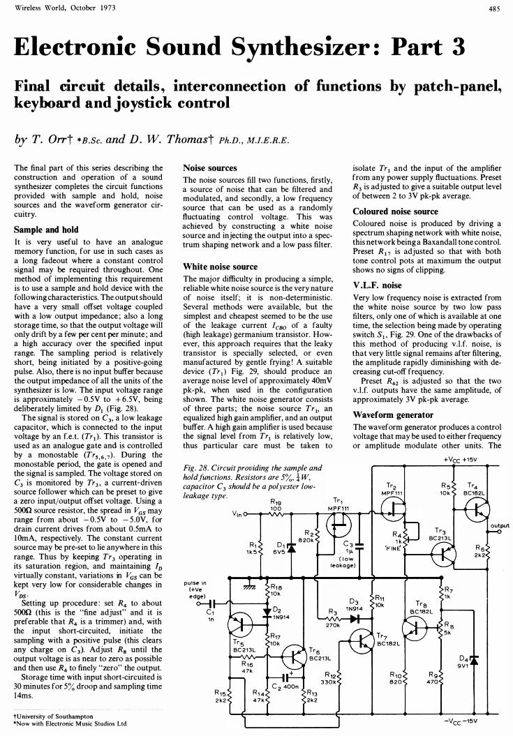
It is very useful to have an analogue memory function, for use in such cases as a long fadeout where a constant control signal may be required throughout. One method of implementing this requirement is to use a sample and hold device with the following characteristics. The output should have a very small offset voltage coupled with a low output impedance ; also a long storage time, so that the output voltage will only drift by a few per cent per minute ; and a high accuracy over the specified input range. The sampling period is relatively short, being initiated by a positive-going pulse. Also, there is no input buffer because the output impedance of all the units of the synthesizer is low. The input voltage range is approximately - 0.5V to + 6.5V, being deliberately limited by DI (Fig. 28).
The signal is stored on C3, a low leakage capacitor, which is connected to the input voltage by an f.e.t. (Trl) . This transistor is used as an analogue gate and is controlled by a monostable (TrS . 6 . 7) . During the mono stable period, the gate is opened and the signal is sampled. The voltage stored on C3 is monitored by Tr3, a current-driven source follower which can be preset to give a zero input/output offset voltage. Using a 500n source resistor, the spread in VGS may range from about - 0.5V to - 5 .0V, for drain current drives from about 0.5mA to I OmA, respectively. The constant current source may be pre-set to lie anywhere in this range. Thus by keeping Tr3 operating in its saturation region, and maintaining ID virtually constant, variations in VGS can be kept very low for considerable changes in VDS ·
Setting up procedure : set R4 to about 500n (this is the "fine adjust" and it is preferable that R4 is a trimmer) and, with the input short-circuited, initiate the sampling with a positive pulse (this clears any charge on C3). Adjust R8 until the output voltage is as near to zero as possible and then use R4 to finely "zero" the output.
Storage time with input short-circuited is 30 minutes for 5% droop and sampling time 14ms.
tUniversity of Southampton 'Now with Electronic Music Studios Ltd
Noise sources
The noise sources fill two functions, firstly, a source of noise that can be filtered and modulated, and secondly, a low frequency source that can be used as a randomly fluctuating control voltage. This was achieved by constructing a white noise source and injecting the output into a spectrum shaping network and a low pass filter.
White noise source
The major difficulty in producing a simple, reliable white noise source is the very nature of noise itself; it is non-deterministic . Several methods were available, but the simplest and cheapest seemed to be the use of the leakage current leHo of a faulty (high leakage) germanium transistor. However, this approach requires that the leaky transistor is specially selected, or even manufactured by gentle frying ! A suitable device ( Tr l ) Fig. 29, should produce an average noise level of approximately 40mV pk-pk, when used in the configuration shown. The white noise generator consists of three parts ; the noise source Tr I> an equalized high gain amplifier, and an output buffer. A high gain amplifier is used because the signal level from Trt is relatively low, thus particular care must be taken to
Fig. 28. Circuit providing the sample and hold/unctions. Resistors are 5%, -! W, capacitor C3 should be a polyester low-leakage type.
R'9
Vln 1 0 0
R 2
R, 0 , 8 20 k
l k 5 6V5
isolate Tr I and the input of the amplifier from any power supply fluctuations. Preset R3 is adjusted to give a suitable output level of between 2 to 3V pk-pk average.
Coloured noise source
Coloured noise is produced by driving a spectrum shaping network with white noise, this network being a Baxandall tone control. Preset R1 7 is adjusted so that with both tone control pots at maximum the output shows no signs of clipping.
V .L.F. noise
Very low frequency noise is extracted from the white noise source by two low pass filters, only one of which is available at one time, the selection being made by operating switch SI ' Fig. 29. One of the drawbacks of this method of producing v.l .f. noise, is that very little signal remains after filtering, the amplitude rapidly diminishing with decreasing cut-off frequency.
Preset R42 is adjusted so that the two v.l .f. outputs have the same amplitude, of approximately 3V pk-pk average.
Waveform generator
The waveform generator produces a control voltage that may be used to either frequency or amplitude modulate other units . The
+Vcc + 1 5V
Tr2 R 5 Tr4 M P F l l l l O k BC182L
Tr3 BC 21 3 L
R 6 ( I ow 2 k 2
leakage)
p u l se i n R' 8 (+Ve
e dge) 1 0 k
<>--1 O2 C , I n l N914
R'7 Tr 5 1 0 k BC 2 1 3 L
R ' 6 4 7 k
R ' 5 R ' 4 C 2 400n
2 k2 4 7 k
R 3
270k
Tr6 B C 2 13L
R , O 8 2 0
R'3 2 k 2
R 7 l k
R 8 5k
04 9 V l
-Vcc -15V
486
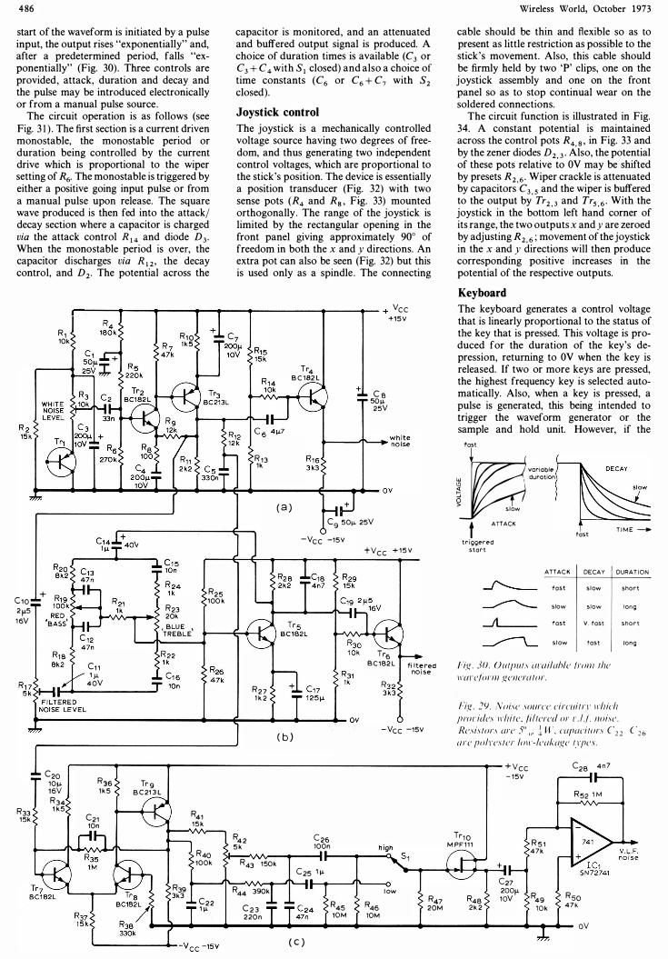
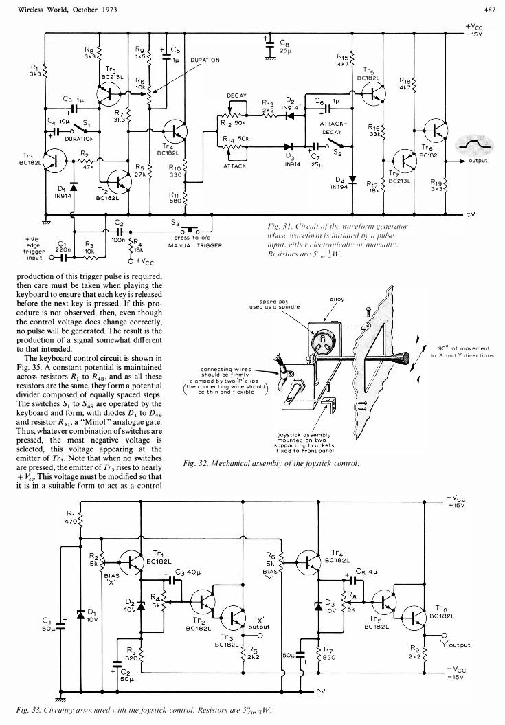
start of the waveform is initiated by a pulse input, the output rises "exponentially" and, after a predetermined period, falls "exponentially" (Fig. 30) . Three controls are provided, attack, duration and decay and the pulse may be introduced electronically or from a manual pulse source.
The circuit operation is as follows (see Fig. 3 1 ) . The first section is a current driven mono stable, the mono stable period or duration being controlled by the current drive which is proportional to the wiper setting of R6. The mono stable is triggered by either a positive going input pulse or from a manual pulse upon release. The square wave produced is then fed into the attack/ decay section where a capacitor is charged via the attack control R I 4 and diode D3 . When the mono stable period is over, the capacitor discharges via R 1 2 , the decay control, and D2 . The potential across the
capacitor is monitored, and an attenuated and buffered output signal is produced. A choice of duration times is available (C3 or C3 + C4 with SI closed) and also a choice of time constants (C6 or C6 + C7 with S2 closed).
Joystick control
The joystick is a mechanically controlled voltage source having two degrees of freedom, and thus generating two independent control voltages, which are proportional to the stick's position. The device is essentially a position transducer (Fig. 32) with two sense pots (R4 and Rs , Fig. 33) mounted orthogonally . The range of the joystick is limited by the rectangular opening in the front panel giving approximately 90° of freedom in both the x and y directions. An extra pot can also be seen (Fig. 32) but this is used only as a spindle . The connecting
;-______ �----�----_.--�----�----------�----��- + Vc c
R I 10k R l O I k 5
R 1 3 I k
Tr4 S C l82 L
+ C s 50 ,..
2SV
+ISV
t-----�--4---�----.. --�--�--�� .. ----------��--_.�-- OV
C l O + 2 ,..S 1 6V
CI I I )J. 40V
R 23 20k , BLU E . T R E B L E
R2 S lOO k
R 2 7 I k 2
( 8 ) C9 SOIJ. 2SV
- VC C -I S V + Vc c + I S V
Tr5 B C I B2 L ti I te red no i se
t---------------------------.. ----�----�--.. ----�� OV ( b ) - VCC -ISV
C20 R35 10 IJ. Tr 9 1 6V I k S B C 21 3 L R 34
R33 I k S I Sk C21 IOn
R41 I S k
R4 2 C 25 S k lOOn
R40 lOOk R43 I SOk
C 2S I ,.. R39 R44 390k low 3k3 C 2 2 C 2 3 R4S R46 I ,..
R47 20M 220 n la M laM
( c )
Wireless World, October 1973 cable should be thin and flexible so as to present as little restriction as possible to the stick's movement. Also, this cable should be firmly held by two 'P' clips, one on the joystick assembly and one on the front panel so as to stop continual wear on the soldered connections.
The circuit function is illustrated in Fig. 34. A constant potential is maintained across the control pots R4• S , in Fig. 33 and by the zener diodes D2 , 3 ' Also, the potential of these pots relative to OV may be shifted by presets R2 , 6 ' Wiper crackle is attenuated by capacitors C3 • S and the wiper is buffered to the output by Tr2 , 3 and TrS . 6 ' With the joystick in the bottom left hand corner of its range, the two outputs x and y are zeroed by adjusting R2 • 6 ; movement of the joystick in the x and y directions will then produce corresponding positive increases in the potential of the respective outputs.
Keyboard
The keyboard generates a control voltage that is linearly proportional to the status of the key that is pressed. This voltage is produced for the duration of the key's depression, returning to OV when the key is released. If two or more keys are pressed, the highest frequency key is selected automatically. Also, when a key is pressed, a pulse is generated, this being intended to trigger the waveform generator or the sample and hold unit. However, if the
tast ��� �";i�t��·n I! � , s l ow
t ATTACK triggered start
ATTAC K fast slow fast
s t ow
fast
DECAY s l ow s low
V. fast
fast
Fig . lO. 011 1/1 1 1 1 .1 l Iwi/lIh/e /roll l /lIe 1 t '{/ / ' ('/iJ I ' I I I ge){el'lI /ol ' .
T I M E _
DURAT ION short l ong
short
long
F/:" . 2CJ . Noise .\(Jul'ce cil'mi/ I' r \ I 'lI icll pro e idl's \ I ·lI i /e. fil/ered or e . l ). ,wisl' . Rl'sis/OI '.1 lire 5;' o. ± W. caflaci/ol's C 2 2 C26 are po/res/er /o l l '-/l'akage l l 'fll'S.
+ V cc C2 B 4 n 7 - I SV R S2 1 M
Trl O R S I M PF I I I 47 k
C27 200,.. R49 R sa R4B 1 0V
2k 2 1 0 k 47 k
oV
Wireless World, October 1973
R, 3 k 3
+ VCC r-----------�----��--�--�--_1�-----------------+�------------------�------.------1�----�---- + 1 5 V
C 8 R 8 3 k 3 1 ",
C3 1 1J..
5 ,
Tr4 R2 B C 1 8 2 L
DURAT I O N
DEC AY
1
R 1 3 2 k 2
25 1-'-
T r5 B C1 8 2 L
487
Tr 1 B C 1 8 2 L
03 I N914 output
47k R 5 R l O 2 7 k 3 3 0
R 1 1 680
AT TAC K Tr7 B C 2 1 3 L R1 9
3 k 3
.----E�----�--4---�----��--�--------------------------�----.. ----.. -----4--- 0V
+ V e edge
tr igger inpu t
C 1 R3 2 2 0 n ,Ok o--t ...----vv'c_
C2
R4 1 Bk + VC C
production o f this trigger pulse i s required, then care must be taken when playing the keyboard to ensure that each key is released before the next key is pressed. If this procedure is not observed, then, even though the control voltage does change correctly, no pulse will be generated. The result is the production of a signal somewhat different to that intended.
The keyboard control circuit is shown in Fig. 35 . A constant potential is maintained across resistors R I to R48 , and as all these resistors are the same, they form a potential divider composed of equally spaced steps . The switches SI to S49 are operated by the keyboard and form, with diodes D I to D49 and resistor R s I , a "Minof" analogue gate. Thus, whatever combination of switches are pressed, the most negative voltage is selected, this voltage appearing at the emitter of Tr3' Note that when no switches are pressed, the emitter of Tr 3 rises to nearly + v.c. This voltage must be modified so that it is in a suitable form to act as a control
press to o/c
M A N U A L T R I G G E R
F,:t: . 3 / . Circl lil ol llll' I m rc!orl l / gCl/culI"r
1 1 1/11,\ 1 ' I m rc!orl l / is il l i l ialcd hi ' a fil llsc il lfi l l l . cillicr clcclro l l ical/ I " or 1 / / ( l / l I lal/ l ' . Resistors ((r(' 5° ( I " l H ',
s p a r e pot u s e d as a s p i n d l e
connecti n g w i re s ---... s hou l d be f i r m l y c l a m p e d b y two l p ' c l i p s (t h e con n e,c t i n g w i r e, S h O U l d)
be t h i n a n d f l eX i b l e
Fig. 32. Mechanical assembly of lhe joyslick conlro/.
90° o f m ov e m e n t
i n X a n d Y d i r e c t i o n s
r-__________ �------------------_1--------------_.--------------------_.--- + vc c + 1 5 V
D1 C 1 + 10V 5 0 1-'-
� ____________________ � ______ � __ � __ � ____________________ -4 ____ - VCC - 1 5 V " __ � __ " __ � __________________________________ " __ "_ O V
Fig. 33. Circuilry £Issoc/alcd l I " illi Ilie juysl /ck cull lrv/. Res/slurs are 5 /0, ± w.
488
Fig. 34. llIustration o!" the joystick control circuit fimction .
Fig. 35. Kevboard control circuit . Switches SI to S49 are operated by the keyboard and
form with diodes Dl to D49 and resistor Rs I , a " Mina!"" analogue gate. Resistors are 5%, i w.
signal. It is attenuated (Rs s), inverted and its d.c. level is shifted (Rs9) so that the range of outputs is from OV to + 3V. Also, the feedback around IC) is such that when no keys are pressed, and the emitter of Tr3 rises to nearly + �C ' the output ( �) is prevented from going negative, and stays at OV.
It is required that a pulse is generated at the moment when a key is pressed, but not when it is released. This would be a simple response to achieve (by detecting the transition direction of the "Minof" voltage) if it were not for the phenomenon of contact bounce. The spikes produced by the bounce can be largely suppressed (C 3) but there is still a possibility of generating a pulse by mistake. One method of overcoming this dilemma is to use a Schmitt trigger with a sizeable hysteresis loop, so that, as the "Minof" signal plus spikes rises or falls, it causes the Schmitt to change state only once. The direction of this change is determined by whether the input is rising or falling (i .e . whether the key is being released or pressed) and can thus be made to produce a pulse only on the falling transient.
Some applications of the keyboard are given in Fig. 36. Fig. 36(a) shows a patch
r----�------�----------------�--_4�-- +Vcc +15V
R49 1 k
+ C1 80p. 050 9V1
+ C2 80 1" 051 9V1
Tr2 R52
2N2904 1k
R50 33 l ow frequency
end of key board
01
� R,
5R1 O2 52
024 524 R24 5R1 025 525
tt� R47 5R1 048 548 R48 5R1 049 549
h igh frequency end of keyboard
R53 33
Tr3 8C182L
052 3V9
Vc key board output
-Vcc �--4---------4---------------------��----�---- - 1 5V
MON05TA B L E
r-_-------...... ----_-- +Vcc + 1 5V
5 C H M ITT
Re8 1 00
Wireless World, October 1973 diagram of simulated piano sound. A sinusoidal signal is given a fast attack and a slow decay. Note that the control output ( �) from the keyboard is modified by the exponential converter, so that an equally tempered scale is produced. However, if the key is prematurely released, the output promptly changes frequency. Fig. 36(b) overcomes this difficulty, by using the sample and hold circuit to store the control signal. Also, reverberation with a slow sinusoidal modulation has been added producing a pleasant effect similar to a xylophone. Fig. 36(c) shows a network for producing bell-like "clanging" noises.
Patch panel
To provide a flexible means of programming the synthesizer, a patch panel similar to the type used in analogue computers has been included. As the input and output impedance of all the units is low, it was possible to use an unscreened system. In fact, ordinary 4mm banana plugs and sockets were eventually chosen, this decision being greatly influenced by cost factors . This choice, however, presents a danger of damage due to misuse. If two outputs are connected together, then it is possible that some damage will eventually occur, although how long it takes is difficult to predict. Certainly, from previous experience of a similar synthesizer, no lasting damage was seen to occur when an error of this sort was made. To minimize this danger the sockets are coloured, all the inputs being yellow, the outputs being any other colour.
The synthesizers on the market appear to have overcome this difficulty, but at some cost. One method is to employ a series of horizontal and parallel conductors, one set being the inputs, the other set the outputs. Pins are then plugged in to make a connection between an input and an output, thus the danger of an "output to output" never arises. Other methods are to use switches or jack plugs instead of pins. These systems are all pre-wired and so another problem, that of the "birds' nest" of patch cords (an all too familiar sight to those who have ever used an analogue computer) has also been eliminated. However, this advantage has been gained at some expense.
The layout of the patch panel was determined on a logical basis ; that is, all the oscillators on one section, the v.c.as and v.c.f. in another, the noise sources in one block etc. Also, to make connections with an external amplifier, a coax. socket was included as well as two sockets which were connected to "ground" potential, these being used as a OV reference point for external equipment such as voltmeters or oscilloscopes.
Power supply
Many units of the synthesizer are sensitive to power supply fluctuations and so a stabilized supply is desirable. The circuit diagram of the supply used is given in Fig. 37. Without this suppression it is possible to trigger a response by switching on and off unconnected (except via the mains) equipment. Care should be taken in constructing the power supply to avoid introducing any high current paths that might adversely affect the circuit operation.
Wireless World, October 1973 Appendix Voltage controlled filter
Consider a band pass filter consisting of a series LCR network. The behaviour of this system is characterized by a linear second order differential equation with constant coefficients. Using analogue techniques, it is possible to model this system, but more important it is possible to make the coefficients variable, in fact, voltage controlled .
The general equation of a linear second order system is
F(t) = x + 2kwnx + w/x
Where Wn is the undamped natural frequency, k is the damping factor (note, the quality factor Q = Ij2k), and F(t) is a generalized forcing function. The solution of this equation consists of two parts ; the particular integral that depends on F(t) , and the complementary function that de� pends on the solution of the right hand side only. Using the network shown in Fig. 38(a) it is possible to implement the complete solution. Different forms of F(t) can be inserted, and by varying pots 4 and 5, the values of w/ and 2kwn can be modified. By monitoring the voltage at the output of integrator I ( - x), the response of a bandpass filter, with the same coefficients, under the influence of the same forcing function F(t) , is observed . (The coefficients for a series LCR circuit would be Wn = I /LC and k = R/2 C/L). By monitoring x, a low pass response would be seen, and x a high pass response. If pot 4 were an electronic
a.c, ma in
Cl 6nS
E� D l 1 00 p. i . v.
C s 2,5 001'
+
+
489 vc
key board ( a ) n p u l se
VC
key board
Jl
key boa r d
Fig. 36 . Three examples olhow the patch-board can be programmed for a particular sound synthesis. See textfO/' explanation .
Fl lA
R l 3 k 3
D 3 I N 9 1 4
Trl BC1S2L
Trl l BC21 3 L
D 5 lN914
R 5 4k?
R 6 IkS
R ? + C6
500 8O�
RS l k
+ Rl2 680 1 W
6 V 0 ' 0 4 A
C 5 lOOn
+ Vcc + 1 5 V
+ 5 V
OV
-VCC t-----�----�--------------------�- 1 5 V Tr?
2N 5l94 Fig. 37. Power supply circuit. Note the use ol the suppressor capacitor Cl to reduce any impulsive interference present on the mains. Resistors are 5%, i W except R I O and R 1 2 which are 1 W. Heat sinks are required by Tr6 (0.6 W dissipation) and Trs and Tr7 (both 1 4 W dissipation) . D I - 4 is a bridge rectifier JOO p.i .v . a t 2A .
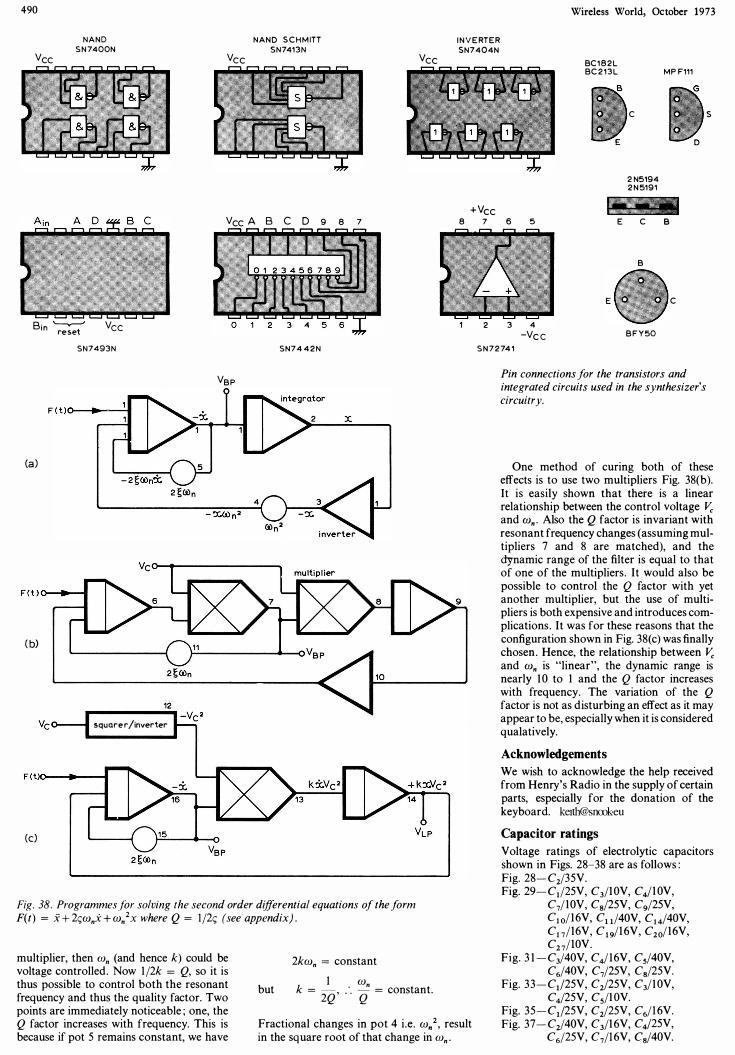
490
Vcc
N A N D S N 7400N
B i n � VCC
Vc c
N A N D S C H M ITT SN741 3 N
Vcc A B C D 9
Vcc
8 7
I N V E RT E R SN7404N
+ VCC 8 7
2
6 5
3 4 -VC C
Wireless World, October 1973
BC 1 8 2 L BC 2 1 3 L
E
c
2 N5194 2 N 5191
C
B
B F Y 50
M P F111
S
B
C
SN7493N S N 7 4 4 2 N S N 7 2 74 1
VB P
F ( t )o--II--:.t 2 x
(a)
4
F ( t ) o-.... -..
( b)
square r/inverter
F ( t)O--... --I
(c)
Fig. 38. Programmes for solving the second order differential equations of the form F(t) = x + 2�wnx + w/x where Q = 1 /2� (see appendix) .
multiplier, then Wn (and hence k) could be voltage controlled. Now 1/2k = Q, so it is thus possible to control both the resonant frequency and thus the quality factor. Two points are immediately noticeable ; one, the Q factor increases with frequency. This is because if pot 5 remains constant, we have
but
2kwn = constant
I Wn k =
2Q ' :. Q = constant.
Fractional changes in pot 4 i .e. wn 2, result
in the square root of that change in Wn .
Pin connections for the transistors and integrated circuits used in the synthesizer's circuitry.
One method of curing both of these effects is to use two multipliers Fig. 38(b). It is easily shown that there is a linear relationship between the control voltage v., and Wn . Also the Q factor is invariant with resonant frequency changes (assuming multipliers 7 and 8 are matched), and the dynamic range of the filter is equal to that of one of the multipliers . It would also be possible to control the Q factor with yet another multiplier, but the use of multipliers is both expensive and introduces complications . It was for these reasons that the configuration shown in Fig. 38(c) was finally chosen . Hence, the relationship between v., and Wn is "linear", the dynamic range is nearly I 0 to I and the Q factor increases with frequency. The variation of the Q factor is not as disturbing an effect as it may appear to be, especially when it is considered qualatively.
Acknowledgements
We wish to acknowledge the help received from Henry's Radio in the supply of certain parts, especially for the donation of the keyboard. kenh@snaJk,eu Capacitor ratings
Voltage ratings of electrolytic capacitors shown in Figs. 28-38 are as follows : Fig. 28- C2/35V. Fig. 29- C1/25V, C3/l OV, CJl OV,
C7/ lOV, Cs/25V, C9/25V, C1 o/ 1 6V, Cl l/40V, CI4/40V, CI 7/l6V, CI9/l 6V, C2o/ l6V, C27/lOV.
Fig. 3 1 - C3/40V, C4/ 16V, Cs/40V, C6/40V, C7/25V, Cs/25V.
Fig. 33-Cd25V, C2/25V, C3/I OV, C4/25V, Cs/l OV.
Fig. 35-Cd2SV, C2/25V, C6/1 6V. Fig. 37- C2/40V, C3/l 6V, CJ25V,
C6/2SV, C7/1 6V, Cs/40V.