Embed Size (px)
Citation preview
Electronic supplementary information (ESI) available
Nonlinear Rashba Spin Splitting in Transition Metal
Dichalcogenide Monolayers
Cai Chenga,b, Jia-Tao Sun*,a, Xiang-Rong Chen*,b, Hui-Xia Fua, Sheng Meng*,a,c
aBeijing National Laboratory for Condensed Matter Physics and Institute of Physics, Chinese Academy of
Sciences, Beijing 100190, China
bCollege of Physical Science and Technology, Sichuan University, Chengdu 610064, China
cSchool of Physical Sciences, University of Chinese Academy of Sciences, Beijing 100190, China
1. Atomic and electronic structures of monolayer TMDs
The atomic structures of the monolayers MXY (M = Mo, W; X, Y = S, Se) is shown in
Figure 1a. When dM-X is equal to dM-Y, MXY becomes non-polar systems, such as MoS2,
MoSe2 and WS2. When dM-X is not equal to dM-Y, MXY denotes for MoSSe with an out-of-
plane dipole moment (Figure S2b). The lattice parameters of MoSSe are a0=3.25 Å, Δd =3.23
Å, dM-X =2.42 Å, dM-Y =2.53 Å, respectively. The lattice constants are well consistent with the
results of Zhu et. al,1 Cheng et. al2 and Zhuang et. al.3 More details structural information is
presented in Table S1. The phonon dispersion of MXY is plotted in Figure S1 No imaginary
frequency indicates that the MXY can be dynamically stable under strong electric field.
Electronic Supplementary Material (ESI) for Nanoscale.This journal is © The Royal Society of Chemistry 2016

Table S1. Structural and electronic parameters of MXY. Lattice constant a0 (Å), layer thickness Δd (Å), the energy difference ΔK-K, ΔK- (denoted in Figure 2 in the main text) without or with spin-orbit coupling (SOC) and spin splitting ΔK-SOC (meV) of the top valence band at K-point.
MXY (SOC) a0 (Å) Δ
d (Å) Δ
K-SOC (meV) Δ
K-K (eV) Δ
K- (meV)
w/o-soc - 1.68 29.7MoS2 w/-soc
3.18 3.13149.0 1.60 100.8
w/o-soc - 1.43 261.7MoSe2 w/-soc
3.32 3.34185.7 1.33 341.6
w/o-soc - 1.81 62.4WS2 w/-soc
3.182 3.14429.8 1.55 257.2
w/o-soc - 1.56 13.9MoSSe
w/-soc3.25 3.23
169.5 1.46 88.8
Figure S1 (a), (c) Phonon dispersion of MoS2 without and with the external electric field. For comparison, the MoSSe and MoSe2 are also shown (b), (d). The absence of imaginary frequency indicates the stability of monolayer TMDs.
Extensive experimental and theoretical studies have been reported on the electronic
structure of few-layer TMDs. The interlayer interaction leads to remarkable modifications of
the electronic and optical properties of MX2. A transition from indirect (bulk or few-layer) to
direct band gap (monolayer) is found.4-6 Moreover, the valence band maximum (VBM) and
conduction band minimum (CBM) are located at the K-point for the monolayer, while the
bulk phase has the VBM at the K point and the CBM along the -K line. According to Table
S1, the monolayers MoS2, MoSe2, WS2 as well as MoSSe are direct band gap semiconductor
independent on including the spin-orbital coupling (SOC). From the Table S1, the band gaps
with the SOC are smaller than these without SOC case. The spin splitting of the uppermost
valence band at K point ΔK-SOC (meV) are 149.0, 169.5, 185.7, and 429.8 in MoS2, MoSSe,
MoSe2 and WS2 respectively.
2. The planar averaged electrostatic potential and dipole moment
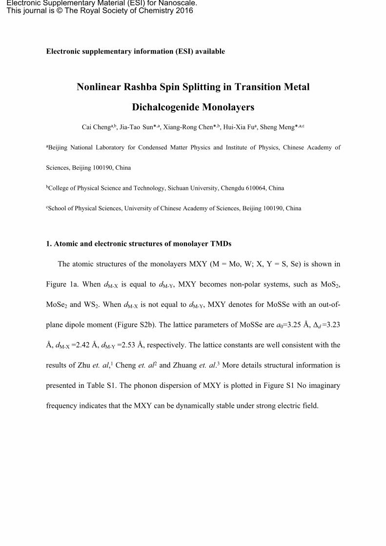
Figure S2 (a) The planar averaged local potential of MoSSe with the external electric field of -0.5 V/Å (red), 0.0 V/Å (olive), and 0.5 V/Å (blue). The potential data are shifted with respect to the vacuum level (zero energy). The intrinsic dipole from S to Se (it is due to the lower potential to higher potential). The inset is the charge density difference between Eext = 0.5 V/Å and Eext = 0 V/Å. Red (blue) color represents the electron accumulation (depletion) region. The isosurface value is set to 0.0038 e/Å3. (b) The dipole moment vary with the extra electric field Eext.
The Rashba effect has been reported in the polar-system MoSSe.2 No Rashba spitting has
been reported in non-polar system MX2 due to the mirror symmetry (x, y, z) →(x, y, -z)
vanishing the potential gradients. The mirror symmetry can be broken by the perpendicular
extra electric field Eext. However the emergence of Rashba effect of MX2 and MoSSe
originates from the potential gradient around the sulfur atoms under the electric field as
described in the main text. In order to distinguish the intrinsic difference of the polar MoSSe
and non-polar MoS2, Figure S2 shows the variation of dipole moment with the extra electric
field Eext, It can be clearly seen that the dipole moment of non-polar MoS2 systems remain
almost unchanged, and the polar MoSSe vary linearly with extra electric field Eext. And it
needed the external negative electric field of Eext = -0.14 V/Å to accommodate the intrinsic
dipole moment.
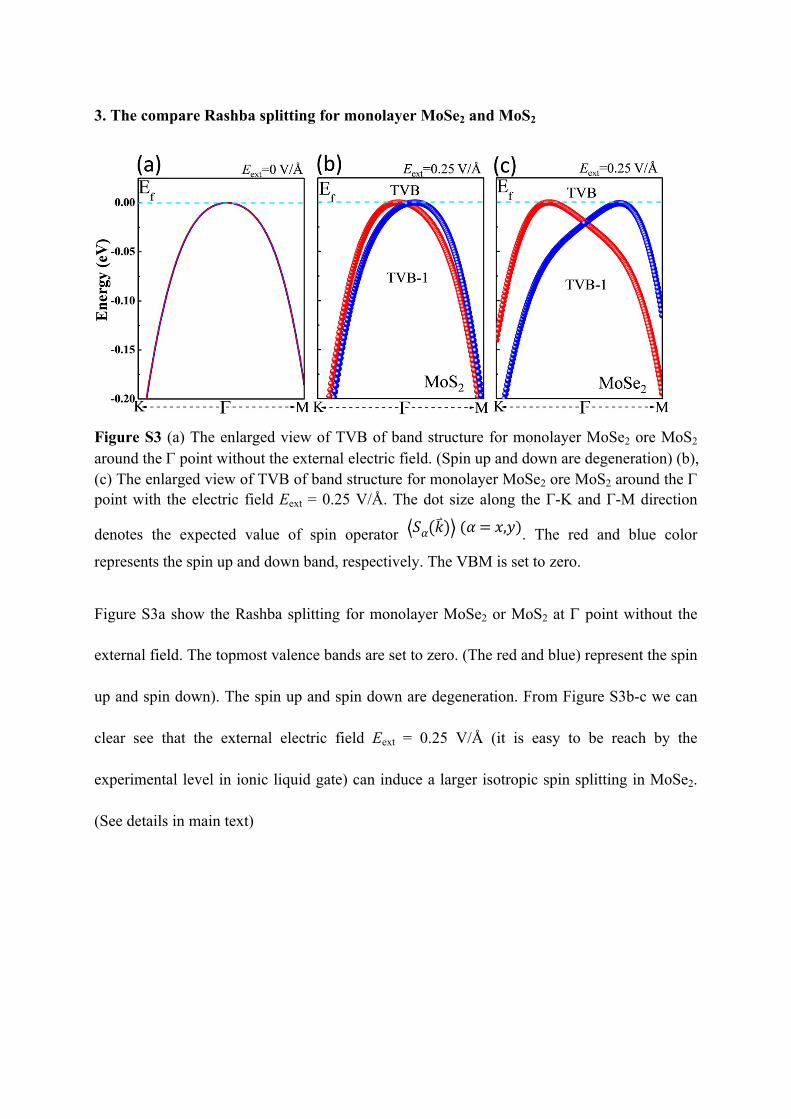
3. The compare Rashba splitting for monolayer MoSe2 and MoS2
Figure S3 (a) The enlarged view of TVB of band structure for monolayer MoSe2 ore MoS2 around the point without the external electric field. (Spin up and down are degeneration) (b), (c) The enlarged view of TVB of band structure for monolayer MoSe2 ore MoS2 around the point with the electric field Eext = 0.25 V/Å. The dot size along the Γ-K and Γ-M direction
denotes the expected value of spin operator . The red and blue color ⟨𝑆𝛼(�⃑�)⟩ (𝛼 = 𝑥,𝑦)
represents the spin up and down band, respectively. The VBM is set to zero.
Figure S3a show the Rashba splitting for monolayer MoSe2 or MoS2 at point without the
external field. The topmost valence bands are set to zero. (The red and blue) represent the spin
up and spin down). The spin up and spin down are degeneration. From Figure S3b-c we can
clear see that the external electric field Eext = 0.25 V/Å (it is easy to be reach by the
experimental level in ionic liquid gate) can induce a larger isotropic spin splitting in MoSe2.
(See details in main text)

4. The Rashba splitting and spin texture for MoSe2
Figure S4 (a) The enlarged view of TVB of band structure for MoSe2 around the point with the increase field Eext = 0.70 V/Å. The dot size along the Γ-K and Γ-M direction denotes the
expected value of spin operator . The red and blue color represents the spin ⟨𝑆𝛼(�⃑�)⟩ (𝛼 = 𝑥,𝑦)
up and down band, respectively. The VBM is set to zero. (b), (c) The energy contour and spin texture of the top valence band TVB and the neighboring band below TVB-1 around the Γ point with electric field Eext = 0.70 V/Å.
Figure 4a show the Rashba splitting for MoSe2 at point with the external field Eext = 0.70
V/Å. The topmost valence bands are set to zero. (The red and blue) represent the spin up and
spin down). Figure S4 b and c show the energy contour and spin texture of the top valence
band (TVB) and its neighboring band (TVB-1) around the point. (See details in main text)
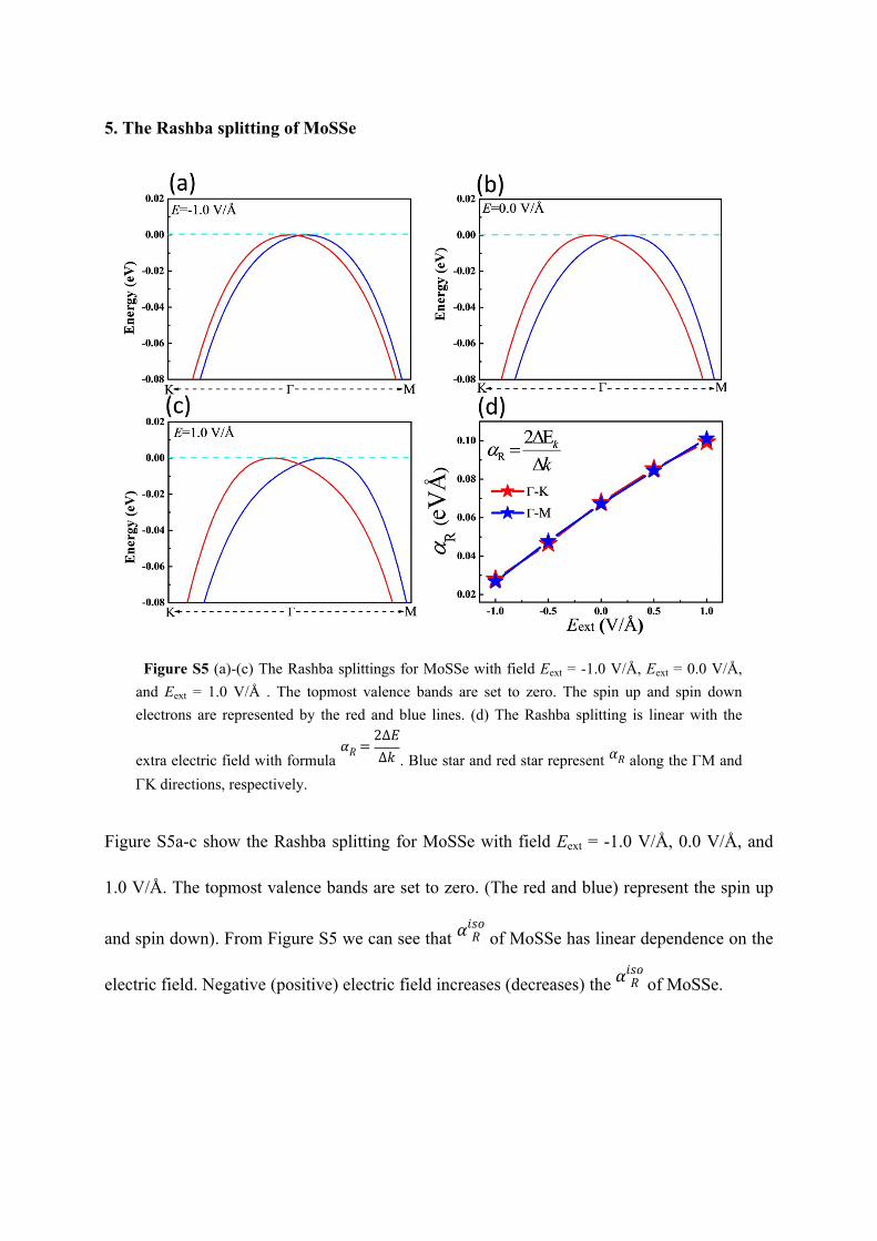
5. The Rashba splitting of MoSSe
Figure S5 (a)-(c) The Rashba splittings for MoSSe with field Eext = -1.0 V/Å, Eext = 0.0 V/Å, and Eext = 1.0 V/Å . The topmost valence bands are set to zero. The spin up and spin down electrons are represented by the red and blue lines. (d) The Rashba splitting is linear with the
extra electric field with formula . Blue star and red star represent along the M and 𝛼𝑅 =
2∆𝐸∆𝑘 𝛼𝑅
K directions, respectively.
Figure S5a-c show the Rashba splitting for MoSSe with field Eext = -1.0 V/Å, 0.0 V/Å, and
1.0 V/Å. The topmost valence bands are set to zero. (The red and blue) represent the spin up
and spin down). From Figure S5 we can see that of MoSSe has linear dependence on the 𝛼𝑖𝑠𝑜𝑅
electric field. Negative (positive) electric field increases (decreases) the of MoSSe.𝛼𝑖𝑠𝑜𝑅

6. The nonlinear Rashba splitting of MoSe2
0.00 0.05 0.10 0.15 0.20 0.250.00
0.06
0.12
0.18
0.24
kk
2
R
Eext (V/Å)
a R eV
Å Se2K Se2M
MoSSe
Figure S6 The linear Rashba parameters calculated by along Γ-K (filled symbols) and Γ-M 𝛼𝑅 =
2∆𝐸∆𝑘
(empty symbols) direction. For comparison, the data for MoSSe are also shown (black stars).
Figure S6 shows the zoom in plot as that in Fig. 4a. It is clearly seen that Rashba spin
splitting of MoSe2 deviates from the linear behavior in the experimentally accessible
conditions (Eext = 0.27 V/Å).

7. The Rashba splitting of MoSe2 and WSe2
Figure S7 The enlarged view of TVB of band structure for MoSe2 and WSe2 under the field Eext = 0.70 V/Å
Figure S7 show the Rashba splitting for MoSe2 (red) and WSe2 (black) with field Eext = 0.70
V/Å. From Figure S5 we clearly see that the anisotropic energy splitting ΔK-M of MoSe2 (22.7
meV) is slightly larger than WSe2 (15.7 meV).

References:
1. Z. Y. Zhu, Y. C. Cheng and U. Schwingenschlögl, Phys. Rev. B 2011, 84, 153402.
2. Y. C. Cheng, Z. Y. Zhu, M. Tahir and U. Schwingenschlögl, EPL (Europhysics Letters)
2013, 102, 57001.
3. H. L. Zhuang and R. G. Hennig, J. Phys. Chem. C 2013, 117, 20440-20445.
4. A. Splendiani, L. Sun, Y. Zhang, T. Li, J. Kim, C. Y. Chim, G. Galli and F. Wang, Nano
Lett. 2010, 10, 1271-1275.
5. S. Tongay, J. Zhou, C. Ataca, K. Lo, T. S. Matthews, J. Li, J. C. Grossman and J. Wu,
Nano Lett. 2012, 12, 5576-5580.
6. Y. Zhang, T. R. Chang, B. Zhou, Y. T. Cui, H. Yan, Z. Liu, F. Schmitt, J. Lee, R. Moore,
Y. Chen, H. Lin, H. T. Jeng, S. K. Mo, Z. Hussain, A. Bansil and Z. X. Shen, Nat.
Nanotechnol. 2014, 9, 111-115.