Embed Size (px)
Citation preview
Electronic transport mechanisms in scaled gate-all-around silicon nanowiretransistor arrays
N. Clement,1,a) X. L. Han (韩相磊),1 and G. Larrieu2,a)1Institute of Electronics, Microelectronics and Nanotechnology, CNRS, Avenue Poincare,59652 Villeneuve d’Ascq, France2Laboratory for Analysis and Architecture of Systems (LAAS), CNRS, Universite de Toulouse,7 Avenue Colonel Roche, 31077 Toulouse, France
(Received 30 October 2013; accepted 9 December 2013; published online 27 December 2013)
Low-frequency noise is used to study the electronic transport in arrays of 14 nm gate length
vertical silicon nanowire devices. We demonstrate that, even at such scaling, the electrostatic
control of the gate-all-around is sufficient in the sub-threshold voltage region to confine charges in
the heart of the wire, and the extremely low noise level is comparable to that of high quality
epitaxial layers. Although contact noise can already be a source of poor transistor operation
above threshold voltage for few nanowires, nanowire parallelization drastically reduces its impact.VC 2013 AIP Publishing LLC. [http://dx.doi.org/10.1063/1.4858955]
Further reduction in the size of the metal-oxide semicon-
ductor field-effect transistors (MOSFETs) used in computer
chips will require more complex geometries to enhance the
gate control of the current flow in the transistor channel.1
Gate-all-around (GAA) is the optimum device configuration
to electrostatically control a transistor with narrowest chan-
nel length2 and minimize the leakage current when the de-
vice is in the off-state, making the device operate with less
dissipation per switching event. Several GAA geometries are
possible and have been demonstrated either in horizontal3 or
vertical configuration.4–7 Although technical solutions are
envisioned to ultimately scale the gate length Lg of transis-
tors down to few nanometers,5 many open questions remain
on the impact of the transition from 1D (either long gate or
large width) to transistors scaled in all dimensions on device
operation. Among them, the quality of devices fabricated
and sources of fluctuation that could induce poor transistor
operation or dispersion in electrical properties should be
addressed clearly to propose solutions for ultimate integra-
tion. However, classical characterization techniques, such as
mobility extraction, are insufficient to provide information
on the devices quality at ultimate scaling, because the
mobility can collapse at such small gate lengths.8–11 Low-
frequency noise can be a very precise technique for charac-
terizing electronic transport in low-noise nanodevices.12,13
Previous studies of low-frequency noise in transistors with a
nanowire (NW) channel have addressed the potential of this
architecture for extremely low noise level. However, they
have either been performed with very long channel14–17 or
on short channel,12,18 but in a specific configuration, not ac-
ceptable for large-scale integration.
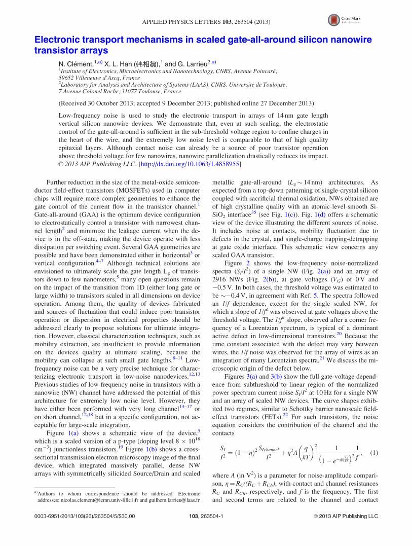
Figure 1(a) shows a schematic view of the device,5
which is a scaled version of a p-type (doping level 8 � 1018
cm�3) junctionless transistors.19 Figure 1(b) shows a cross-
sectional transmission electron microscopy image of the final
device, which integrated massively parallel, dense NW
arrays with symmetrically silicided Source/Drain and scaled
metallic gate-all-around (Lg� 14 nm) architectures. As
expected from a top-down patterning of single-crystal silicon
coupled with sacrificial thermal oxidation, NWs obtained are
of high crystalline quality with an atomic-level-smooth Si-
SiO2 interface35 (see Fig. 1(c)). Fig. 1(d) offers a schematic
view of the device illustrating the different sources of noise.
It includes noise at contacts, mobility fluctuation due to
defects in the crystal, and single-charge trapping-detrapping
at gate oxide interface. This schematic view concerns any
scaled GAA transistor.
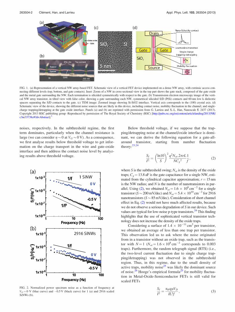
Figure 2 shows the low-frequency noise-normalized
spectra (SI/I2) of a single NW (Fig. 2(a)) and an array of
2916 NWs (Fig. 2(b)), at gate voltages (VG) of 0V and
�0.5V. In both cases, the threshold voltage was estimated to
be ��0.4V, in agreement with Ref. 5. The spectra followed
an 1/f dependence, except for the single scaled NW, for
which a slope of 1/f2 was observed at gate voltages above the
threshold voltage. The 1/f2 slope, observed after a corner fre-
quency of a Lorentzian spectrum, is typical of a dominant
active defect in low-dimensional transistors.20 Because the
time constant associated with the defect may vary between
wires, the 1/f noise was observed for the array of wires as an
integration of many Lorentzian spectra.21 We discuss the mi-
croscopic origin of the defect below.
Figures 3(a) and 3(b) show the full gate-voltage depend-
ence from subthreshold to linear region of the normalized
power spectrum current noise SI/I2 at 10Hz for a single NW
and an array of scaled NW devices. The curve shapes exhib-
ited two regimes, similar to Schottky barrier nanoscale field-
effect transistors (FETs).22 For such transistors, the noise
equation considers the contribution of the channel and the
contacts
SII2
¼ 1� gð Þ2 SIchannelI2
þ g2Aq
kT
� �2 1
1� e�qgVdkT
� �2 1f ; (1)
where A (in V2) is a parameter for noise-amplitude compari-
son, g¼RC/(RCþRCh), with contact and channel resistances
RC and RCh, respectively, and f is the frequency. The first
and second terms are related to the channel and contact
a)Authors to whom correspondence should be addressed. Electronic
addresses: [email protected] and [email protected]
0003-6951/2013/103(26)/263504/5/$30.00 VC 2013 AIP Publishing LLC103, 263504-1
APPLIED PHYSICS LETTERS 103, 263504 (2013)
noises, respectively. In the subthreshold regime, the first
term dominates, particularly when the channel resistance is
large (we can consider g� 0 at VG� 0V). As a consequence,
we first analyse results below threshold voltage to get infor-
mation on the charge transport in the wire and gate-oxide
interface and then address the contact noise level by analyz-
ing results above threshold voltage.
Below threshold voltage, if we suppose that the trap-
ping/detrapping noise at the channel/oxide interface is domi-
nant, we can derive the following equation for a gate-all-
around transistor, starting from number fluctuation
theory:23,24
SII2
¼ ln10
S
� �2q2Not:2prL
NCg2
1
f; (2)
where S is the subthreshold swing; Not is the density of the oxide
traps; Cg¼ 13.8 aF is the gate capacitance for a single NW, esti-
mated from the cylindrical capacitor approximation; r¼ 15 nm
is the NW radius; and N is the number of nanotransistors in par-
allel. Using (2), we obtained Not¼ 1.6 � 108 cm�2 for a single
transistor (S� 200mV/dec) and Not¼ 5.4� 1010 cm�2 for 2916
nanotransistors (S� 85mV/dec). Consideration of short channel
effect in Eq. (2) would not have much affected results, because
we do not observe a serious degradation of S in our device. Suchvalues are typical for low-noise p-type transistors.24 This finding
highlights that the use of sophisticated vertical transistor tech-
nology does not increase the density of the oxide traps.
Considering a surface of 1.4 � 10�11 cm2 per transistor,
we obtained an average of less than one trap per transistor.
This observation led us to ask where the noise originated
from in a transistor without an oxide trap, such as the transis-
tor with N¼ 1 (Not¼ 1.6� 108 cm�2 corresponds to 0.003
traps). Furthermore, the random telegraph signal (RTS) (i.e.,
the two-level current fluctuation due to single charge trap-
ping/detrapping) was not observed in the subthreshold
region. Thus, in this regime, due to the small density of
active traps, mobility noise25 was likely the dominant source
of noise.26 Hooge’s empirical formula25 for mobility fluctua-
tion in Metal-Oxide-Semiconductor FETs is still valid for
scaled FETs
SII2
¼ aHqlVD
IL2f; (3)
FIG. 1. (a) Representation of a vertical NW array-based FET. Schematic view of a vertical FET device implemented on a dense NW array, with extrinsic access con-
necting different levels (top, bottom, and gate contacts). Inset: Zoom of a NW in cross-sectional view in the top part shows the gate stack, composed of the gate oxide
and the metal gate surrounding the NW. Each termination is silicided symmetrically with respect to the gate. (b) Transmission electron microscopy image of the verti-
cal NW array transistor, in tilted view with false color, showing a gate surrounding each NW, symmetrical silicided S/D (PtSi) contacts and 60-nm low k dielectric
spacers separating the S/D contacts to the gate. (c) TEM image: Zoomed image showing Si-SiO2 interface. Vertical axis corresponds to the (100) crystal axis. (d)
Schematic view of the device, showing the different noise sources that are likely in this device, including contact noise, mobility fluctuation in the channel, and single-
charge trapping/detrapping at the gate oxide interface. Panels (a) and (b) are reprinted with permission from G. Larrieu and X.-L. Han, Nanoscale 5, 2437 (2013).
Copyright 2013 RSC publishing group -Reproduced by permission of The Royal Society of Chemistry (RSC) [http://pubs.rsc.org/en/content/articlelanding/2013/NR/
c3nr33738c#!divAbstract].5
FIG. 2. Normalized power spectrum noise as a function of frequency at
VG¼ 0 V (blue curve) and �0.5V (black curve) for 1 (a) and 2916 scaled
SiNWs (b).
263504-2 Clement, Han, and Larrieu Appl. Phys. Lett. 103, 263504 (2013)
where aH is the Hooge’s constant, l is the mobility, and
VD¼ 50mV is the drain voltage. We obtained
10�5< aH< 5� 10�5 for 1 or 2916 scaled NWs at
1< l< 5 cm2/V s. In high-quality material, such as epitaxial
layers, aH values range from 10�6 to 10�4.26 Consequently,
the mobility degradation observed in these devices was
unlikely to be related to low crystal quality (Fig. 1(c)) or
poor oxide interfaces. This small Hooge’s constant is the
smallest ever reported for scaled nanowire transistors. For
example aH� 4.2 � 10�3 was found for a GAA (35 nm gate
length) transistor with a III-V NW.27 For gate lengths below
15 nm, we can not compare our results since there was no
report of Hooge’s constant at such scaling. In the subthres-
hold region, we can reasonably consider that mobility fluctu-
ation was the dominant source of noise. More importantly,
the observed absence of RTS and low noise amplitude indi-
cated a “volume” conduction. Although such transport in the
heart of the wire has already been suggested for long
NWs15,17 with junctionless architecture or due to quantum
confinement effect (our argument based on RTS is only
meaningful for scaled devices), it was not ensured that such
behavior would have been observed for GAA transistors
with Lg< 15 nm. This clearly indicates the potential of such
GAA technology for future scaling.
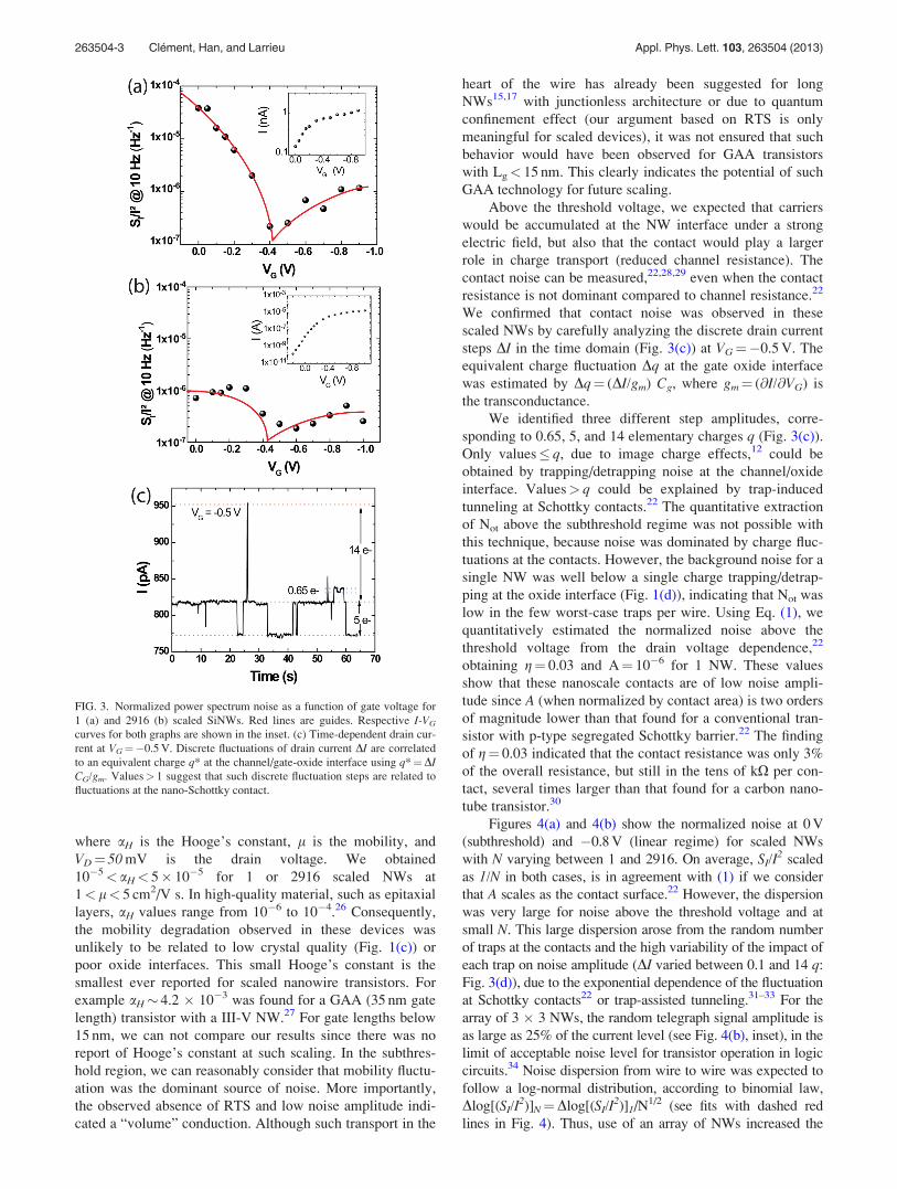
Above the threshold voltage, we expected that carriers
would be accumulated at the NW interface under a strong
electric field, but also that the contact would play a larger
role in charge transport (reduced channel resistance). The
contact noise can be measured,22,28,29 even when the contact
resistance is not dominant compared to channel resistance.22
We confirmed that contact noise was observed in these
scaled NWs by carefully analyzing the discrete drain current
steps DI in the time domain (Fig. 3(c)) at VG¼�0.5V. The
equivalent charge fluctuation Dq at the gate oxide interface
was estimated by Dq¼ (DI/gm) Cg, where gm¼ (@I/@VG) is
the transconductance.
We identified three different step amplitudes, corre-
sponding to 0.65, 5, and 14 elementary charges q (Fig. 3(c)).
Only values� q, due to image charge effects,12 could be
obtained by trapping/detrapping noise at the channel/oxide
interface. Values> q could be explained by trap-induced
tunneling at Schottky contacts.22 The quantitative extraction
of Not above the subthreshold regime was not possible with
this technique, because noise was dominated by charge fluc-
tuations at the contacts. However, the background noise for a
single NW was well below a single charge trapping/detrap-
ping at the oxide interface (Fig. 1(d)), indicating that Not was
low in the few worst-case traps per wire. Using Eq. (1), we
quantitatively estimated the normalized noise above the
threshold voltage from the drain voltage dependence,22
obtaining g¼ 0.03 and A¼ 10�6 for 1 NW. These values
show that these nanoscale contacts are of low noise ampli-
tude since A (when normalized by contact area) is two orders
of magnitude lower than that found for a conventional tran-
sistor with p-type segregated Schottky barrier.22 The finding
of g¼ 0.03 indicated that the contact resistance was only 3%
of the overall resistance, but still in the tens of kX per con-
tact, several times larger than that found for a carbon nano-
tube transistor.30
Figures 4(a) and 4(b) show the normalized noise at 0V
(subthreshold) and �0.8V (linear regime) for scaled NWs
with N varying between 1 and 2916. On average, SI/I2 scaled
as 1/N in both cases, is in agreement with (1) if we consider
that A scales as the contact surface.22 However, the dispersion
was very large for noise above the threshold voltage and at
small N. This large dispersion arose from the random number
of traps at the contacts and the high variability of the impact of
each trap on noise amplitude (DI varied between 0.1 and 14 q:Fig. 3(d)), due to the exponential dependence of the fluctuation
at Schottky contacts22 or trap-assisted tunneling.31–33 For the
array of 3 � 3 NWs, the random telegraph signal amplitude is
as large as 25% of the current level (see Fig. 4(b), inset), in the
limit of acceptable noise level for transistor operation in logic
circuits.34 Noise dispersion from wire to wire was expected to
follow a log-normal distribution, according to binomial law,
Dlog[(SI/I2)]N¼Dlog[(SI/I
2)]1/N1/2 (see fits with dashed red
lines in Fig. 4). Thus, use of an array of NWs increased the
FIG. 3. Normalized power spectrum noise as a function of gate voltage for
1 (a) and 2916 (b) scaled SiNWs. Red lines are guides. Respective I-VG
curves for both graphs are shown in the inset. (c) Time-dependent drain cur-
rent at VG¼�0.5V. Discrete fluctuations of drain current DI are correlated
to an equivalent charge q* at the channel/gate-oxide interface using q*¼DICG/gm. Values> 1 suggest that such discrete fluctuation steps are related to
fluctuations at the nano-Schottky contact.
263504-3 Clement, Han, and Larrieu Appl. Phys. Lett. 103, 263504 (2013)
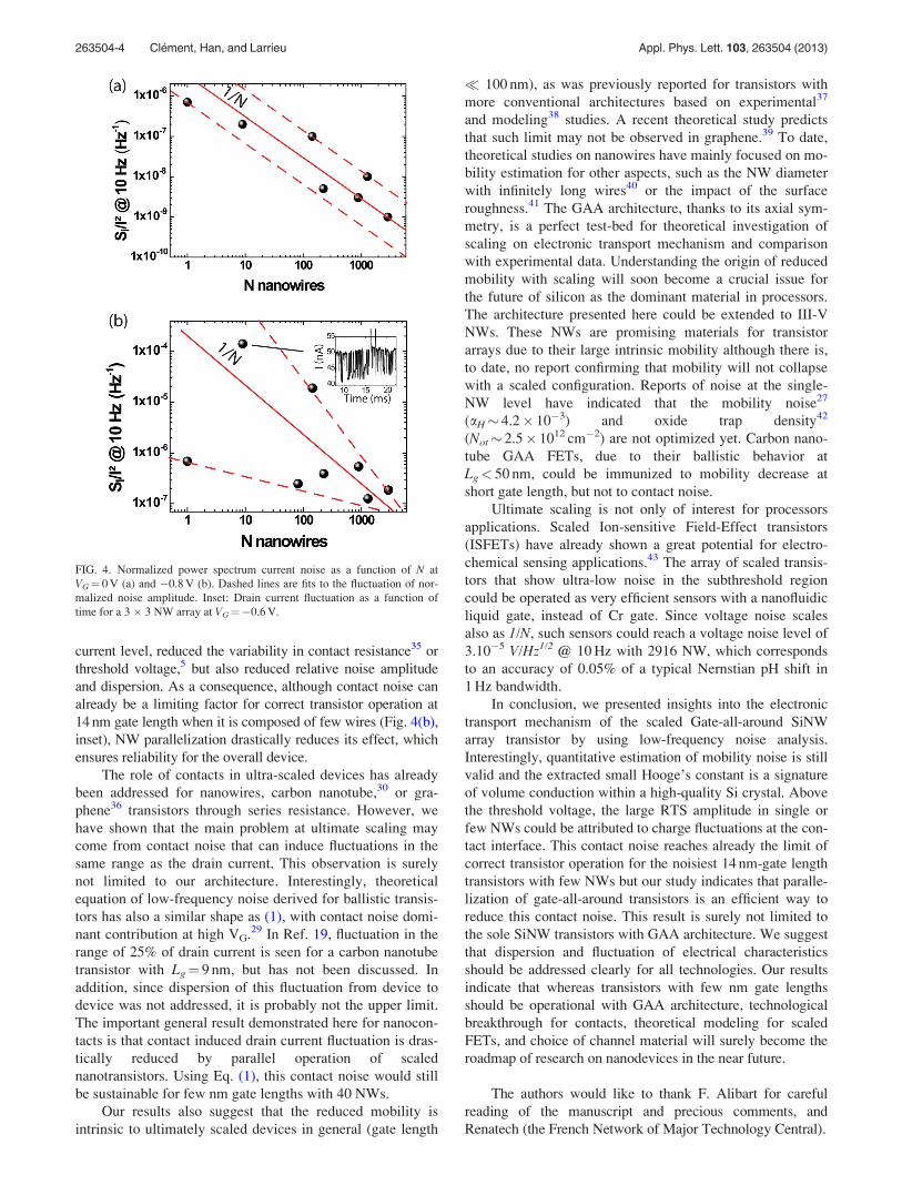
current level, reduced the variability in contact resistance35 or
threshold voltage,5 but also reduced relative noise amplitude
and dispersion. As a consequence, although contact noise can
already be a limiting factor for correct transistor operation at
14 nm gate length when it is composed of few wires (Fig. 4(b),
inset), NW parallelization drastically reduces its effect, which
ensures reliability for the overall device.
The role of contacts in ultra-scaled devices has already
been addressed for nanowires, carbon nanotube,30 or gra-
phene36 transistors through series resistance. However, we
have shown that the main problem at ultimate scaling may
come from contact noise that can induce fluctuations in the
same range as the drain current. This observation is surely
not limited to our architecture. Interestingly, theoretical
equation of low-frequency noise derived for ballistic transis-
tors has also a similar shape as (1), with contact noise domi-
nant contribution at high VG.29 In Ref. 19, fluctuation in the
range of 25% of drain current is seen for a carbon nanotube
transistor with Lg¼ 9 nm, but has not been discussed. In
addition, since dispersion of this fluctuation from device to
device was not addressed, it is probably not the upper limit.
The important general result demonstrated here for nanocon-
tacts is that contact induced drain current fluctuation is dras-
tically reduced by parallel operation of scaled
nanotransistors. Using Eq. (1), this contact noise would still
be sustainable for few nm gate lengths with 40 NWs.
Our results also suggest that the reduced mobility is
intrinsic to ultimately scaled devices in general (gate length
� 100 nm), as was previously reported for transistors with
more conventional architectures based on experimental37
and modeling38 studies. A recent theoretical study predicts
that such limit may not be observed in graphene.39 To date,
theoretical studies on nanowires have mainly focused on mo-
bility estimation for other aspects, such as the NW diameter
with infinitely long wires40 or the impact of the surface
roughness.41 The GAA architecture, thanks to its axial sym-
metry, is a perfect test-bed for theoretical investigation of
scaling on electronic transport mechanism and comparison
with experimental data. Understanding the origin of reduced
mobility with scaling will soon become a crucial issue for
the future of silicon as the dominant material in processors.
The architecture presented here could be extended to III-V
NWs. These NWs are promising materials for transistor
arrays due to their large intrinsic mobility although there is,
to date, no report confirming that mobility will not collapse
with a scaled configuration. Reports of noise at the single-
NW level have indicated that the mobility noise27
(aH� 4.2� 10�3) and oxide trap density42
(Not� 2.5� 1012 cm�2) are not optimized yet. Carbon nano-
tube GAA FETs, due to their ballistic behavior at
Lg< 50 nm, could be immunized to mobility decrease at
short gate length, but not to contact noise.
Ultimate scaling is not only of interest for processors
applications. Scaled Ion-sensitive Field-Effect transistors
(ISFETs) have already shown a great potential for electro-
chemical sensing applications.43 The array of scaled transis-
tors that show ultra-low noise in the subthreshold region
could be operated as very efficient sensors with a nanofluidic
liquid gate, instead of Cr gate. Since voltage noise scales
also as 1/N, such sensors could reach a voltage noise level of
3.10�5 V/Hz1/2 @ 10Hz with 2916 NW, which corresponds
to an accuracy of 0.05% of a typical Nernstian pH shift in
1Hz bandwidth.
In conclusion, we presented insights into the electronic
transport mechanism of the scaled Gate-all-around SiNW
array transistor by using low-frequency noise analysis.
Interestingly, quantitative estimation of mobility noise is still
valid and the extracted small Hooge’s constant is a signature
of volume conduction within a high-quality Si crystal. Above
the threshold voltage, the large RTS amplitude in single or
few NWs could be attributed to charge fluctuations at the con-
tact interface. This contact noise reaches already the limit of
correct transistor operation for the noisiest 14 nm-gate length
transistors with few NWs but our study indicates that paralle-
lization of gate-all-around transistors is an efficient way to
reduce this contact noise. This result is surely not limited to
the sole SiNW transistors with GAA architecture. We suggest
that dispersion and fluctuation of electrical characteristics
should be addressed clearly for all technologies. Our results
indicate that whereas transistors with few nm gate lengths
should be operational with GAA architecture, technological
breakthrough for contacts, theoretical modeling for scaled
FETs, and choice of channel material will surely become the
roadmap of research on nanodevices in the near future.
The authors would like to thank F. Alibart for careful
reading of the manuscript and precious comments, and
Renatech (the French Network of Major Technology Central).
FIG. 4. Normalized power spectrum current noise as a function of N at
VG¼ 0V (a) and �0.8V (b). Dashed lines are fits to the fluctuation of nor-
malized noise amplitude. Inset: Drain current fluctuation as a function of
time for a 3 � 3 NW array at VG¼�0.6V.
263504-4 Clement, Han, and Larrieu Appl. Phys. Lett. 103, 263504 (2013)
1M. Lundstrom, Science 299, 210 (2003).2C. Cress and S. Datta, Science 341, 140 (2013).3J. J. Gu, Y. Q. Liu, Y. Q. Wu, R. Colby, R. G. Gordon, and P. D. Ye,
Tech. Dig. - Int. Electron Devices Meet. 2011, 769.4K. Tomioka, M. Yoshimura, and T. Fukui, Nature 488, 189 (2012).5G. Larrieu and X.-L. Han, Nanoscale 5, 2437 (2013).6C. Thelander, L. E. Froberg, C. Rehnstedt, L. Samuelson, and L.-E.
Wernersson, IEEE Electron Device Lett. 29, 206 (2008).7V. Schmidt, H. Riel, S. Senz, S. Karg, W. Riess, and U. Gosele, Small 2,85 (2006).
8G. Bidal, D. Fleury, G. Ghibaudo, F. Boeuf, and T. Skotnicki, in
Proceedings of Silicon Nanoelectronics Workshop (SNW) (IEEE, Kyoto,Japan, 2009), pp. 5–6.
9A. Cros, K. Romanjek, D. Fleury, S. Harrison, R. Cerutti, P. Coronel, B.
Dumont, A. Pouydebasque, R. Wacquez, B. Duriez et al., Tech. Dig. - Int.Electron Devices Meet. 2006, 663.
10M. Yang, E. P. Gusev, M. Ieong, O. Gluschenkov, D. C. Boyd, K. K.
Chan, P. M. Kozlowski, C. P. D’Emic, R. M. Sicina, P. C. Jamison, and A.
I. Chou, IEEE Electron Device Lett. 24, 339 (2003).11A. Majumdar, S. Bangsaruntip, G. M. Cohen, L. M. Gignac, M. Guillorn,
M. M. Frank, J. W. Sleight, and D. A. Antoniadis, Tech. Dig. - Int.
Electron Devices Meet. 2012, 179.12N. Clement, K. Nishiguchi, A. Fujiwara, and D. Vuillaume, Nature
Commun. 1, 92 (2010).13A. A. Balandin, Nat. Nanotechnol. 8, 549 (2013).14W. Feng, R. Hettiarachchi, Y. Lee, S. Sato, K. Kakushima, M. Sato, K.
Fukuda, M. Niwa, K. Yamabe, K. Shiraishi, H. Iwai, and K. Ohmori,
Tech. Dig. - Int. Electron Devices Meet. 2011, 630.15S.-H. Lee, C.-K. Baek, S. Park, D.-W. Kim, D. K. Sohn, J.-S. Lee, D. M.
Kim, and Y.-H. Jeong, IEEE Electron Device Lett. 33, 1348 (2012).16A. N. Nazarov, I. Ferain, N. D. Akhavan, P. Razavi, R. Yu, and J. P.
Colinge, Appl. Phys. Lett. 98, 092111 (2011).17A. N. Nazarov, I. Ferain, N. D. Akhavan, P. Razavi, R. Yu, and J. P.
Colinge, Appl. Phys. Lett. 99, 073502 (2011).18N. Clement, K. Nishiguchi, J.-F. Dufreche, D. Guerin, A. Fujiwara, and D.
Vuillaume, Appl. Phys. Lett. 98, 014104 (2011).19J.-P. Colinge, C.-W. Lee, A. Afzalian, N. D. Akhavan, R. Yan, P. Razavi,
B. O’Neill, A. Blake, M. White, A.-M. Kelleher, B. McCarthy, and R.
Murphy, Nat. Nanotechnol. 5, 225 (2010).20M. J. Kirton and M. J. Uren, Adv. Phys. 38, 367 (1989).21S. Machlup, J. Appl. Phys. 25, 341 (1954).22N. Clement, G. Larrieu, and E. Dubois, IEEE Trans. Electron Devices 59,180 (2012).
23G. Ghibaudo, Solid-State Electron. 32, 563 (1989).24C. Jakobson, I. Bloom, and Y. Nemirovsky, Solid-State Electron. 42, 1807(1998).
25F. N. Hooge, Phys. Lett. A 29, 139 (1969).26L. K. J. Vandamme and F. N. Hooge, IEEE Trans. Electron Devices 55,3070 (2008).
27K.-M. Persson, E. Lind, A. W. Dey, C. Thelander, H. Sjoland, and L.-E.
Wernersson, IEEE Electron Device Lett. 31, 428 (2010).28M. Peransin, P. Vignaud, D. Rigaud, and L. K. J. Vandamme, IEEE Trans.
Electron Devices 37, 2250 (1990).29J. Tersoff, Nano Lett. 7, 194 (2007).30A. D. Franklin, M. Luisier, S.-J. Han, G. Tulevski, C. M. Breslin, L.
Gignac, M. S. Lundstrom, and W. Haensch, Nano Lett. 12, 758
(2012).31A. Avellan, W. Krautschneider, and S. Schwantes, Appl. Phys. Lett. 78,2790 (2001).
32F. Martinez, S. Soliveres, C. Leyris, and M. Valenza, in IEEE ICMTSProceedings (IEEE, 2006), p. 193.
33N. Clement, S. Pleutin, O. Seitz, S. Lenfant, and D. Vuillaume, Phys. Rev.
B 76, 205407 (2007).34M.-L. Fan, V. P.-H. Hu, Y.-N. Chen, P. Su, and C.-T. Chuang,
“Investigation of single-trap-induced random telegraph noise for tunnel
FET Based devices, 8t sram cell, and sense amplifiers,” in Proceedings of
the 2013 IEEE International Reliability Physics Symposium (IRPS),
Monterey, CA, USA, April 2013.35X. L. Han, G. Larrieu, E. Dubois, and F. Cristiano, Surf. Sci. 606, 836(2012).
36Y. Wu, V. Perebeinos, Y.-M. Lin, T. Low, F. Xia, and P. Avouris, Nano
Lett. 12, 1417 (2012).37J. Ramos, E. Augendre, A. Kottantharayil, A. Mercha, E. Simoen, M.
Rosmeulen, S. Severi, C. Kerner, T. Chiarella, A. Nackaerts, I. Ferain, T.
Hoffmann, M. Jurczak, and S. Biesemans, “Experimental evidence of
short-channel electron mobility degradation caused by interface charges
located at the gate-edge of triple-gate finFETs,” in Proceedings of the 8th
International Conference on Solid-State and Integrated-Circuit
Technology, Shanghai, China, 23–26 October 2006.38K. Huet, J. Saint-Martin, A. Bournel, S. Galdin-Retailleau, P. Dollfus, G.
Ghibaudo, and M. Mouis, in Proceedings of Solid State Device ResearchConference, ESSDERC (2007), p. 382.
39J. Zheng, L. Wang, Q. Quhe, Q. Liu, H. Li, D. Yu, W. N. Mei, J. Shi, Z.
Gao, and J. Lu, Sci. Rep. 3, 1314 (2013).40Y.-M. Niquet, H. Mera, and C. Delerue, Appl. Phys. Lett. 100, 153119(2012).
41C. Buran, M. G. Pala, M. Bescond, M. Dubois, and M. Mouis, IEEE
Trans. Electron Devices 56, 2186 (2009).42T. Muramatsu, K. Miura, Y. Shiratori, Z. Yatabe, and S. Kasai, Jpn. J.
Appl. Phys., Part 1 51, 06FE18 (2012).43N. Clement, K. Nishiguchi, J.-F. Dufreche, D. Guerin, A. Fujiwara, and D.
Vuillaume, Nano Lett. 13, 3903 (2013).
263504-5 Clement, Han, and Larrieu Appl. Phys. Lett. 103, 263504 (2013)