Embed Size (px)
Citation preview

Solid State Detectors and Electronics – Electronics II Helmuth SpielerTRIUMF Summer Institute 2007 LBNL
1
Electronics II
1. Threshold Discriminator SystemsNoise rateEfficiency vs. Occupancy
2. Timing MeasurementsTime JitterTime WalkPulse Shaping
3. Elements of Digital ElectronicsLogic functionsLogic circuitryPower dissipationTiming problems
4. Digitization of Pulse Height and Time– Analog to Digital Conversion
ResolutionDifferential non-linearityIntegral non-linearityConversion timeCount-rate performanceStabilityAnalog-to-digital conversion techniques
5. Time digitizers
6. Digital Signal Processing
7. Readout Systems

Solid State Detectors and Electronics – Electronics II Helmuth SpielerTRIUMF Summer Institute 2007 LBNL
2
1. Threshold Discriminator Systems
The simplest form of a digitzed readout is a threshold discriminator system, which produces anormalized (digital) output pulse when the input signal exceeds a certain level.
Noise affects not only the resolution of amplitude measurements, but also the determines the minimumdetectable signal threshold.
Consider a system that only records the presence of a signal if it exceeds a fixed threshold.
PREAMPLIFIER SHAPER THRESHOLDDISCRIMINATOR
THRESHOLD LEVEL V
DETECTOR
TH
TH
OUTPUT
V
How small a detector pulse can still be detected reliably?

Solid State Detectors and Electronics – Electronics II Helmuth SpielerTRIUMF Summer Institute 2007 LBNL
3
Consider the system at times when no detector signal is present.
Noise will be superimposed on the baseline.
Some noise pulses will exceed the threshold.This is always true since the amplitude spectrum of Gaussian noise extends to infinity
TIME
THRESHOLD

Solid State Detectors and Electronics – Electronics II Helmuth SpielerTRIUMF Summer Institute 2007 LBNL
4
The threshold must be set
1. high enough to suppress noise hits
2. low enough to capture the signal
PULSE HEIGHT
CO
UN
T R
ATE
NOISE
SIGNAL
THRESHOLD
Solid State Detectors and Electronics – Electronics II Helmuth SpielerTRIUMF Summer Institute 2007 LBNL
5
With the threshold level set to 0 relative to the baseline, all of the positive excursions will be recorded.
Assume that the desired signals are occurring at a certain rate.If the detection reliability is to be >99%, for example, then the rate of noise hits must be less than 1%of the signal rate.
The rate of noise hits can be reduced by increasing the threshold.
If the system were sensitive to pulse magnitude alone, the integral over the Gaussian distribution(the error function) would determine the factor by which the noise rate 0nf is reduced.
2( / 2 )
0
1
2n
T
Q Qn
n Qn
fe dQ
f Q π
∞−= ∫ ,
where
Q is the equivalent signal charge,
Qn the equivalent noise charge and
QT the threshold level.
However, since the pulse shaper broadens each noise impulse, the time dependence is equallyimportant. For example, after a noise pulse has crossed the threshold, a subsequent pulse will not berecorded if it occurs before the trailing edge of the first pulse has dropped below threshold.

Solid State Detectors and Electronics – Electronics II Helmuth SpielerTRIUMF Summer Institute 2007 LBNL
6
Combined probability function
Both the amplitude andtime distribution areGaussian.
The rate of noise hits isdetermined by integratingthe combined probabilitydensity function in theregime that exceeds thethreshold.
This yields
2 2/ 20
T nQ Qn nf f e−= ⋅
Of course, one can just aswell use thecorresponding voltagelevels.
What is the noise rate atzero threshold fn0 ?
TIME
AMPLITUDE
THRESHOLD
P (A )
P (t )
BASELINE

Solid State Detectors and Electronics – Electronics II Helmuth SpielerTRIUMF Summer Institute 2007 LBNL
7
For a system with the frequency response ( )A f the frequency of zeros
2 2
2 00
2
0
( )4
( )
f A f dff
A f df
∞
∞= ⋅∫
∫
(Rice, Bell System Technical Journal, 23 (1944) 282 and 24 (1945) 46)
Since we are interested in the number of positive excursions exceeding the threshold, 0nf is ½ thefrequency of zero-crossings.
For an ideal band-pass filter with lower and upper cutoff frequencies f1 and f2 the noise rate
3 32 1
02 1
12
3f f
ff f−
=−
For a CR-RC filter with i dτ τ= the ratio of cutoff frequencies of the noise bandwidth is
2
1
4.5ff
=
so to a good approximation one can neglect the lower cutoff frequency and treat the shaper as a low-pass filter, i.e. 1 0f = .

Solid State Detectors and Electronics – Electronics II Helmuth SpielerTRIUMF Summer Institute 2007 LBNL
8
Then 0 2
2
3f f=
An ideal bandpass filter has infinitely steep slopes, so the upper cutoff frequency 2f must be replacedby the noise bandwidth.
The noise bandwidth of an RC low-pass filter with time constant τ is14nf τ
∆ =
Setting 2 nf f= ∆ yields the frequency of zeros 0
1
2 3f
τ=
and the frequency of noise hits vs. threshold
2 2 2 2 2 2/ 2 / 2 / 200
12 4 3
th n th n th nQ Q Q Q Q Qn n
ff f e e e
τ− − −= ⋅ = ⋅ = ⋅
Thus, the required threshold-to-noise ratio for a given frequency of noise hits nf is
2log(4 3 )Tn
n
Qf
Qτ= −

Solid State Detectors and Electronics – Electronics II Helmuth SpielerTRIUMF Summer Institute 2007 LBNL
9
Note that product of noise rate and shaping time nf τ determines the required threshold-to-noise ratio, i.e. for a given threshold-to-noise ratio the noise rate is higher at short shapingtimes
⇒ The noise rate for a given threshold-to-noise ratio is proportional to bandwidth.
⇒ To obtain the same noise rate, a fast system requires a larger threshold-to-noise ratiothan a slow system with the same noise level.

Solid State Detectors and Electronics – Electronics II Helmuth SpielerTRIUMF Summer Institute 2007 LBNL
10
Efficiency vs. Occupancy
Frequently a threshold discriminator system is used in conjunction with other detectors that provideadditional information, for example the time of a desired event.
In a collider detector the time of beam crossings is known, so the output of the discriminator is sampledat specific times.
The number of recorded noise hits then depends on
1. the sampling frequency (e.g. bunch crossing frequency) Sf
2. the width of the sampling interval t∆ , which is determined by the time resolution of the system.
The product Sf t∆ determines the fraction of time the system is open to recording noise hits, so the rateof recorded noise hits is S nf t f∆ .
Often it is more interesting to know the probability of finding a noise hit in a given interval, i.e. theoccupancy of noise hits, which can be compared to the occupancy of signal hits in the same interval.
This is the situation in a storage pipeline, where a specific time interval is read out after a certaindelay time (e.g. trigger latency)
The occupancy of noise hits in a time interval t∆ :2 2/ 2
2 3T nQ Q
n n
tP t f e
τ−∆
= ∆ ⋅ = ⋅
i.e. the occupancy falls exponentially with the square of the threshold-to-noise ratio.

Solid State Detectors and Electronics – Electronics II Helmuth SpielerTRIUMF Summer Institute 2007 LBNL
11
Example of noise occupancy (open circles) and efficiency (solid circles) vs. threshold in apractical detector module:
Note that an extended overlap region of high efficiency and low noise occupancy is desired.
0
20
40
60
80
100
0 50 100 150 200 250
THRESHOLD [mV]
EFF
ICIE
NC
Y [%
]
1E-05
1E-04
1E-03
1E-02
1E-01
1E+00
OFF-TR
AC
K O
CC
UP
AN
CY
Solid State Detectors and Electronics – Electronics II Helmuth SpielerTRIUMF Summer Institute 2007 LBNL
12
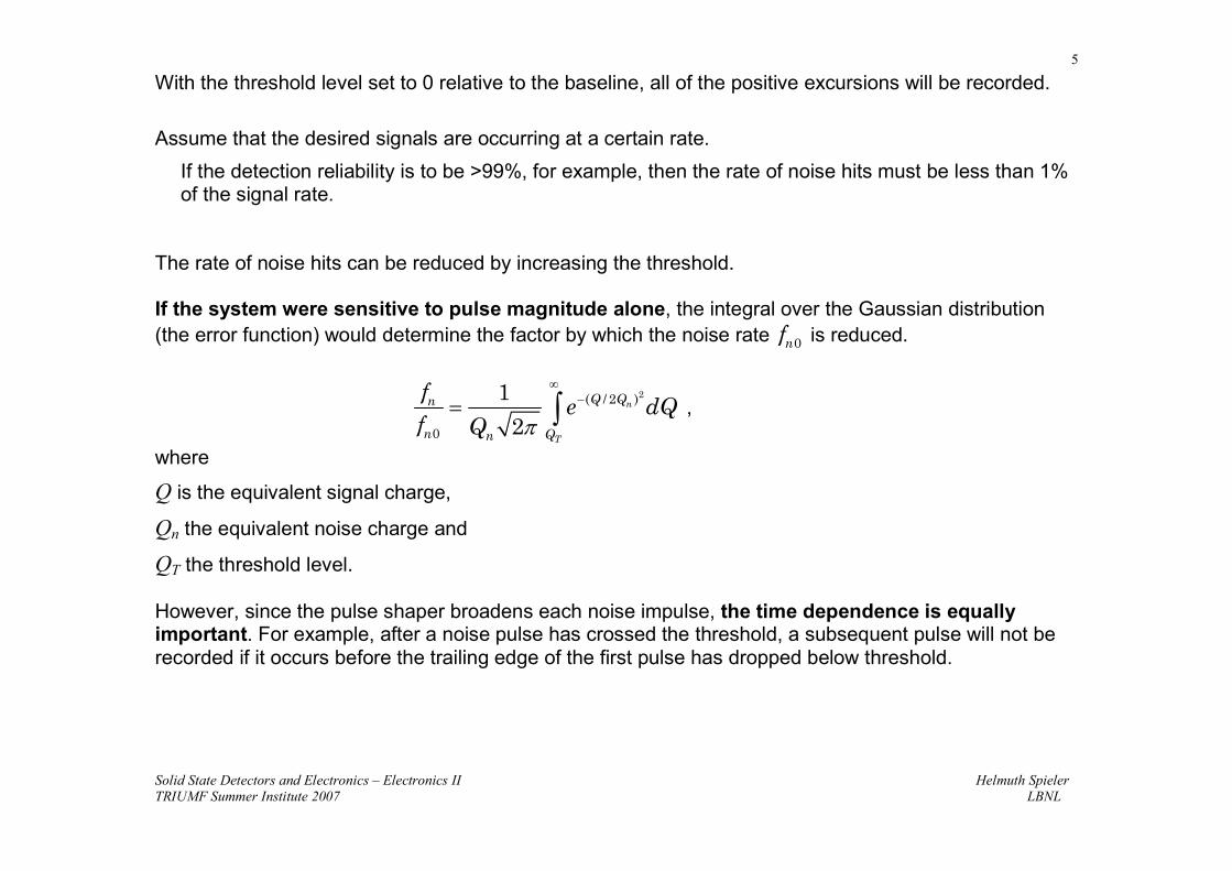
The dependence of occupancyon threshold can be used tomeasure the noise level.
21
log log22 3
Tn
n
QtP
Qτ ∆
= −
,
so the slope of log nP vs. 2TQ
yields the noise level.
This analysis is independentof the details of the shaper,which affect only the offset.
0.1 0.2 0.3 0.4 0.5 0.6 0.7 0.8 0.9 1.0 1.1
THRESHOLD SQUARED [ fC2 ]
1x10⁻⁶
1x10⁻⁵
1x10⁻⁴
1x10⁻³
1x10⁻²
1x10⁻¹
NO
ISE
OC
CU
PAN
CY
Qn = 1320 e

Solid State Detectors and Electronics – Electronics II Helmuth SpielerTRIUMF Summer Institute 2007 LBNL
13
2. Timing Measurements
Pulse height measurements discussed up to now emphasize accurate measurement ofsignal charge.
• Timing measurements optimize determination of time of occurrence.
• For timing, the figure of merit is not signal-to-noise, but slope-to-noise ratio.
Consider the leading edge of a pulse fed into a threshold discriminator (comparator).
The instantaneous signal level is modulated byby noise.
⇒ time of threshold crossing fluctuates
/
T
n rt
V
tdV S Ndt
σσ = ≈
rt = rise time
Typically, the leading edge is not linear, so theoptimum trigger level is the point of maximumslope.
TIMEA
MP
LITU
DE
VT 2σ
2σ
n
t

Solid State Detectors and Electronics – Electronics II Helmuth SpielerTRIUMF Summer Institute 2007 LBNL
14
Pulse Shaping
Consider a system whose bandwidth is determined by a single RC integrator.The time constant of the RC low-pass filter determines the
• rise time (and hence dV/dt)• amplifier bandwidth (and hence the noise)
Time dependence: /0( ) (1 )t
oV t V e τ−= −
The rise time is commonly expressed as the interval between the points of 10% and90% amplitude
2.2rt τ=In terms of bandwidth
2.2 0.352.2
2ru u
tf f
τπ
= = =
Example: An oscilloscope with 100 MHz bandwidth has 3.5 ns rise time.
For a cascade of amplifiers: 2 2 21 2 ...r r r rnt t t t≈ + + +
Solid State Detectors and Electronics – Electronics II Helmuth SpielerTRIUMF Summer Institute 2007 LBNL
15
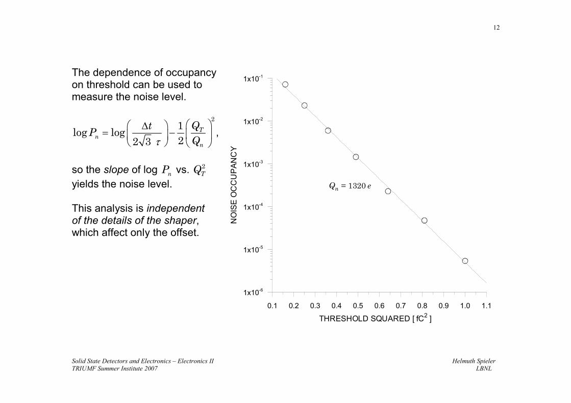
Choice of Rise Time in a Timing System
Assume a detector pulse with peak amplitude V0 and a rise time tc passing through anamplifier chain with a rise time tra.
1. amplifier rise time � signal rise time:
Noise 1
1
ura
ura
ft
dVf
dt t
∝ ∝
∝ ∝
increase in bandwidth ⇒ improvement in /dV dt outweighs increase in noise.
2. amplifier rise time � signal rise time
increase in noise without increase in /dV dt
Optimum: The amplifier rise time should be chosen to match the signal rise time.
Differentiation time constant: choose greater than rise time constant( int10diffτ τ= incurs 20% loss in pulse height)

Solid State Detectors and Electronics – Electronics II Helmuth SpielerTRIUMF Summer Institute 2007 LBNL
16
Time Walk
For a fixed trigger level the time of thresholdcrossingdepends on pulse amplitude.
⇒ Accuracy of timing measurement limited by
• jitter (due to noise)
• time walk (due to amplitude variations)
If the rise time is known, “time walk” can be compensated in software event-by-event bymeasuring the pulse height and correcting the time measurement.
This technique fails if both amplitude and rise time vary, as is common.
In hardware, time walk can be reduced by setting the threshold to the lowest practical level,or by using amplitude compensation circuitry, e.g. constant fraction triggering.
TIME
AM
PLI
TUD
E
VT
∆T = “WALK”
Solid State Detectors and Electronics – Electronics II Helmuth SpielerTRIUMF Summer Institute 2007 LBNL
17
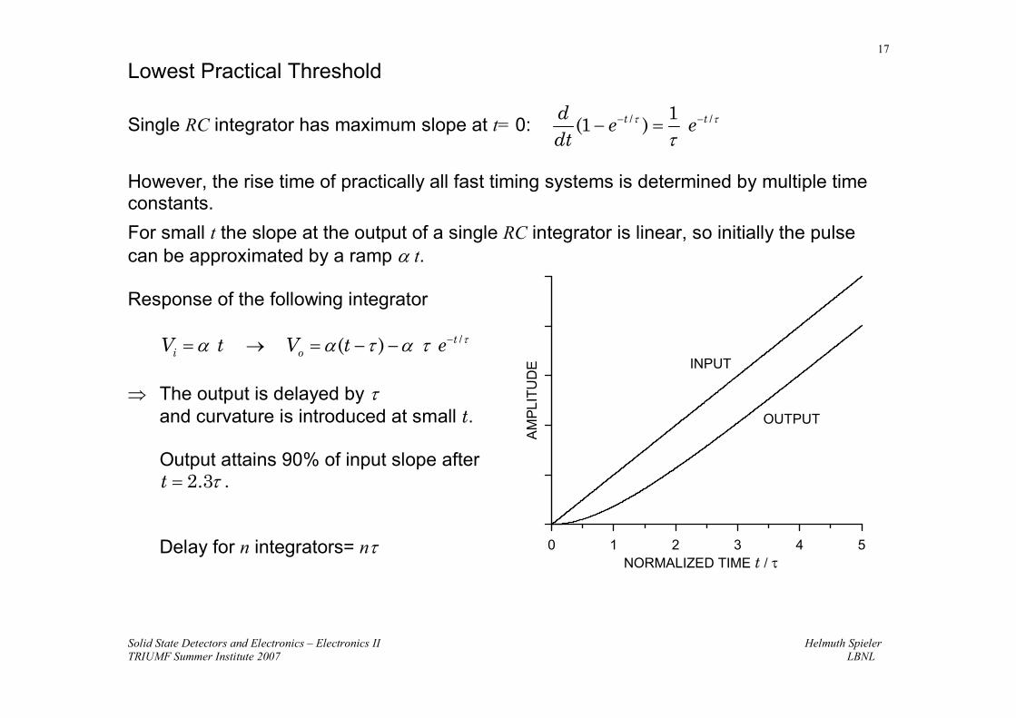
Lowest Practical Threshold
Single RC integrator has maximum slope at t= 0: / /1(1 )t td
e edt
τ τ
τ− −− =
However, the rise time of practically all fast timing systems is determined by multiple timeconstants.For small t the slope at the output of a single RC integrator is linear, so initially the pulsecan be approximated by a ramp α t.
Response of the following integrator
/( ) ti oV t V t e τα α τ α τ −= → = − −
⇒ The output is delayed by τand curvature is introduced at small t.
Output attains 90% of input slope after2.3t τ= .
Delay for n integrators= nτ 0 1 2 3 4 5NORMALIZED TIME t / τ
AM
PLIT
UD
E INPUT
OUTPUT

Solid State Detectors and Electronics – Electronics II Helmuth SpielerTRIUMF Summer Institute 2007 LBNL
18
Additional RC integrators introduce more curvature at the beginning of the pulse.
Output pulse shape for multiple RCintegrators
(normalized to preserve thepeaking time, 1 /n n nτ τ −= )
Increased curvature at beginning of pulse limits the minimum threshold for good timing.
⇒ One dominant time constant best for timing measurements
Unlike amplitude measurements, where multiple integrators are desirable to improvepulse symmetry and count rate performance.
0 1TIME
0.0
0.2
0.4
0.6
0.8
1.0
SHAP
ER O
UTP
UT
n=8
n=1
n=2
n=4
Solid State Detectors and Electronics – Electronics II Helmuth SpielerTRIUMF Summer Institute 2007 LBNL
19
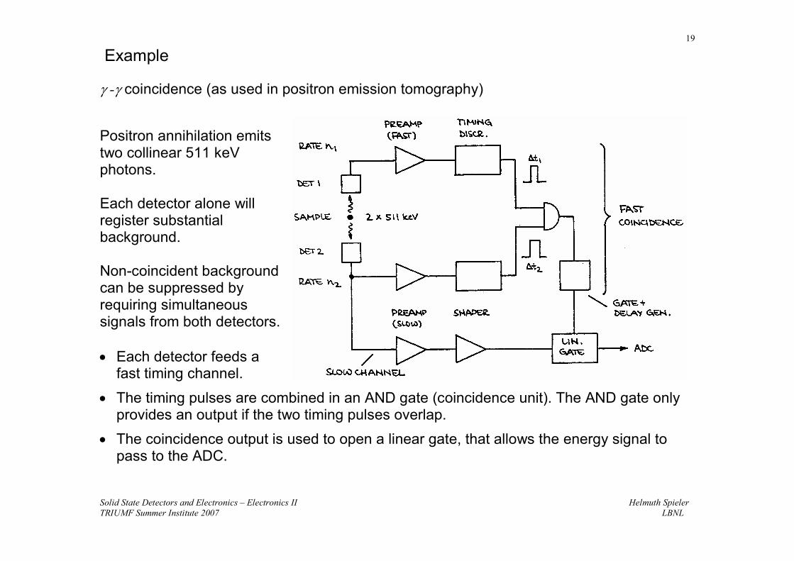
Example
γ -γ coincidence (as used in positron emission tomography)
Positron annihilation emitstwo collinear 511 keVphotons.
Each detector alone willregister substantialbackground.
Non-coincident backgroundcan be suppressed byrequiring simultaneoussignals from both detectors.
• Each detector feeds afast timing channel.
• The timing pulses are combined in an AND gate (coincidence unit). The AND gate onlyprovides an output if the two timing pulses overlap.
• The coincidence output is used to open a linear gate, that allows the energy signal topass to the ADC.

Solid State Detectors and Electronics – Electronics II Helmuth SpielerTRIUMF Summer Institute 2007 LBNL
20
This arrangement accommodates the contradictory requirements of timing and energymeasurements. The timing channels can be fast, whereas the energy channel can use slowshaping to optimize energy resolution (“fast-slow coincidence”).
Chance coincidence rate
Two random pulse sequences have some probability of coincident events.
If the event rates in the two channels are n1 and n2, and the timing pulse widths are ∆t1and ∆t2, the probability of a pulse from the first source occurring in the totalcoincidence window is
1 1 1 2( )P n t t= ⋅ ∆ + ∆
The coincidence is “sampled” at a rate n2 , so the chance coincidence rate is
1 2
1 2 1 2( )c
c
n P n
n n n t t
= ⋅
= ⋅ ⋅ ∆ + ∆
i.e. in the arrangement shown above, the chance coincidence rate increases with thesquare of the source strength.
Example: 1 2n n= = 106 s-1
1 2t t∆ = ∆ = 5 ns ⇒ cn = 104 s-1

Solid State Detectors and Electronics – Electronics II Helmuth SpielerTRIUMF Summer Institute 2007 LBNL
21
Fast Timing: Comparison between theory and experiment
Time resolution 1/( / )S N∝
At S/N<100 the measured curve liesabove the calculation because thetiming discriminator limited the rise time.
At high S/N the residual jitter of the timedigitizer limits the resolution.
For more details on fast timing with semiconductor detectors, see
H. Spieler, IEEE Trans. Nucl. Sci. NS-29/3 (1982) 1142.
10 100 1000SIGNAL-TO-NOISE RATIO
1
10
100
1000
TIM
ER
ES
OLU
TIO
N(p
srm
s)
MEASURED
CALCULATED

Solid State Detectors and Electronics – Electronics II Helmuth SpielerTRIUMF Summer Institute 2007 LBNL
22
Improved Timing at Low Temperatures?
Carrier mobility increases at low temperatures.
Electron drift velocity in Si:(low doping levels)
solid: (111)E
dashed: (100)E
Jacobini et al. Solid State Elec 20/2 (1977) 77-89
At low fields ~10-fold increase, but saturation velocity at 77K only increases 30%,so at the high fields optimal for timing only modest improvement.
Ionization coefficient α(77K)/α(300K) ≈ 2, so maximum bias voltage reduced.

Solid State Detectors and Electronics – Electronics II Helmuth SpielerTRIUMF Summer Institute 2007 LBNL
23
1. Elements of Digital Electronics
Basic differences
Analog signals have variable amplitude
Digital have constant amplitude, but variable timing
Presence of signal at specific times is evaluated:(does the signal level exceed threshold?)
Transmission capacity of a digital link (bits per second)
Shannon’s theorem: B = BandwidthS = Signal (pulse amplitude)N = Noise
Noise enters, because near the switching threshold, digital elements are amplifiers.
If the noise is due to cross-talk from other digital signals,increasing the pulse amplitude will not improve S/N
Digital electronics not just a matter of “yes” or “no” – real systems must also deal with“maybe”.
TIME
VTH
2log 1S
C BN
= ⋅ +

Solid State Detectors and Electronics – Electronics II Helmuth SpielerTRIUMF Summer Institute 2007 LBNL
24
Logic Functions
OUTPUT IS HIGH WHEN BOTH INPUTS ARE HIGH.
OUTPUT IS HIGH WHEN ANY INPUT IS HIGH.
When outputs inverted: NAND and NOR
AND
AB
A
B
OR
AB
A
B

Solid State Detectors and Electronics – Electronics II Helmuth SpielerTRIUMF Summer Institute 2007 LBNL
25
Logic Functions cont’d
OUTPUT IS HIGH WHEN ONLY ONE INPUT IS HIGH.
LEVEL AT D INPUT IS STORED AT POSITIVE CLOCK (CLK) TRANSITION.AMBIGUITY WHEN D AND CLK TRANSITIONS ARE SIMULTANEOUS.
D FLIP FLOP(LATCH)
D
CLK
Q
D
CLK
Q
?
EXCLUSIVEOR
AB
A
B

Solid State Detectors and Electronics – Electronics II Helmuth SpielerTRIUMF Summer Institute 2007 LBNL
26
LOGIC CIRCUITRY - Modern logic uses MOS technology.
CMOS – combine NMOS and PMOS ⇒ significant power reduction
V
V
V
DD
DD
DD
0
0
NMOS
V
V
V
DD
DD
DD
0
0
PMOS
Transistor conducts when input is high. PMOS: Transistor conducts when input is low.
CMOS Inverter
V
V V
DD
DD DD
0 0
CMOS
Current flows only during transition.
CMOS NAND GateV
V
V
V
DD
DD
DD
DD
0
0
0

Solid State Detectors and Electronics – Electronics II Helmuth SpielerTRIUMF Summer Institute 2007 LBNL
27
LOGIC ARRAYS
Complex logic systems are not designed using individual gates.
Instead, logic functions are described in a high-level language (e.g. VHDL) and synthesizedusing design libraries (in custom ICs, “ASICs”) or programmable logic arrays.
Typical: 512 pads usable for inputs and outputs, ~106 gates, ~100K memory
Software also generates “test vectors” that can be used to test finished parts.
LOGIC ARRAYINPUTS OUTPUTS

Solid State Detectors and Electronics – Electronics II Helmuth SpielerTRIUMF Summer Institute 2007 LBNL
28
POWER DISSIPATION ANDPROPAGATION DELAYS
Energy dissipated in wiring resistance R:
( )
2
22
0
( )
( ) exp
1exp 2 /
2
E i t R dt
V ti t
R RC
VE t RC dt CV
R
∞
=
= −
= − =
∫
∫If pulses (rising + falling edge transitions)occur at frequency f ,
2P fCV=
Power dissipation increases withclock frequency and (logic swing)2.
RC time constant also introduces timedelay in addition to propagation delay ofgates/buffers!
Depends on wiring resistance and totalload capacitance(number of connected inputs).
CASCADED CMOS STAGES
EQUIVALENT CIRCUIT
R
C
T T+ t∆
V VTH TH
WIRINGRESISTANCE
SUM OF INPUTCAPACITANCES
i
0
V
Solid State Detectors and Electronics – Electronics II Helmuth SpielerTRIUMF Summer Institute 2007 LBNL
29
TIMING PROBLEMS
Fast logic is time-critical!
Valid results depend on maintaining minimumoverlaps (e.g. AND)set-up times (latches)
Each logic circuit has a finite propagation delay.This delay also depends on circuit loading, i.e. how many loads the circuit has to drive.
In addition, wiring resistance introduces delayDepends on: number of circuits connected to wire/trace
length of tracematerial
Relying on control of circuit and wiring delays to maintain timing requires great care!Dependent on circuit variations, temperature
Most designers fail at this!
More robust: synchronous systems, where timing of all transitions is determined bymaster clock.

Solid State Detectors and Electronics – Electronics II Helmuth SpielerTRIUMF Summer Institute 2007 LBNL
30
2. Digitization of Pulse Height and Time – Analog to Digital Conversion
For data storage and subsequent analysis the analog signal at the shaper output must be digitized.
Important parameters for ADCs used in detector systems:1. Resolution
The “granularity” of the digitized output2. Differential Non-Linearity
How uniform are the digitization increments?3. Integral Non-Linearity
Is the digital output proportional to the analog input?4. Conversion Time
How much time is required to convert an analog signal to a digital output?5. Count-Rate Performance
How quickly can a new conversion commence after completion of a prior one withoutintroducing deleterious artifacts?
6. StabilityDo the conversion parameters change with time?
Instrumentation ADCs used in industrial data acquisition and control systems share most of theserequirements. However, detector systems place greater emphasis on differential non-linearity and count-rate performance. The latter is important, as detector signals often occur randomly, in contrast tomeasurement systems where signals are sampled at regular intervals.

Solid State Detectors and Electronics – Electronics II Helmuth SpielerTRIUMF Summer Institute 2007 LBNL
31
1. Resolution
Digitization incurs approximation, as a continuous signal distribution is transformed into a discrete set ofvalues. To reduce the additional errors (noise) introduced by digitization, the discrete digital steps mustcorrespond to a sufficiently small analog increment.
Simplistic assumption:
Resolution is defined by the number of output bits, e.g. 13 bits → 411.2 10
8192V
V−∆
= = ⋅
True Measure: Channel ProfilePlot probability vs. pulse amplitude that a pulse height corresponding to a specific output bin isactually converted to that address.
Ideal ADC:
Measurement accuracy:
• If all counts of a peak fall in one bin, theresolution is ∆V.
• If the counts are distributed over several bins,peak fitting can yield a resolution of10-1 – 10-2 ∆V,if the distribution is known and reproducible (notnecessarily a valid assumption for an ADC). V VV i ii +∆V
∆V∆V ∆V
∆V
1
P V( )i

Solid State Detectors and Electronics – Electronics II Helmuth SpielerTRIUMF Summer Institute 2007 LBNL
32
In reality, the channel profile is not rectangular as sketched above.
Electronic noise in the threshold discrimination process that determines the channel boundaries“smears” the transition from one bin to the next.
Measured channel profile (13 bit ADC) The profiles of adjacent channelsoverlap
CHANNEL BOUNDARIES
P V( )
V 344 345 346 347 348 349 350CHANNEL NUMBER
0
1
PR
OB
AB
ILIT
Y
Solid State Detectors and Electronics – Electronics II Helmuth SpielerTRIUMF Summer Institute 2007 LBNL
33
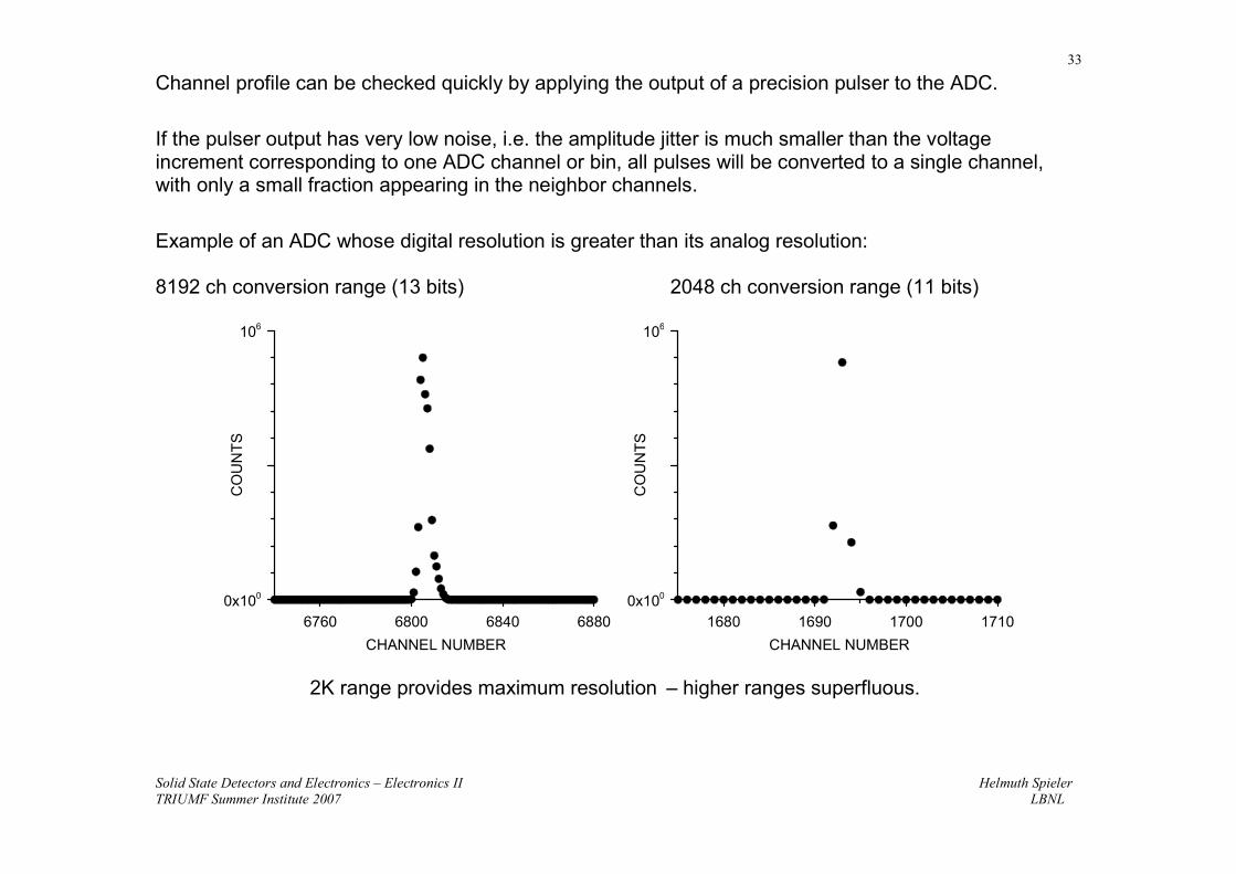
Channel profile can be checked quickly by applying the output of a precision pulser to the ADC.
If the pulser output has very low noise, i.e. the amplitude jitter is much smaller than the voltageincrement corresponding to one ADC channel or bin, all pulses will be converted to a single channel,with only a small fraction appearing in the neighbor channels.
Example of an ADC whose digital resolution is greater than its analog resolution:
8192 ch conversion range (13 bits) 2048 ch conversion range (11 bits)
6760 6800 6840 6880CHANNEL NUMBER
0x100
106
CO
UN
TS
1680 1690 1700 1710CHANNEL NUMBER
0x100
106
CO
UN
TS
2K range provides maximum resolution – higher ranges superfluous.
Solid State Detectors and Electronics – Electronics II Helmuth SpielerTRIUMF Summer Institute 2007 LBNL
34
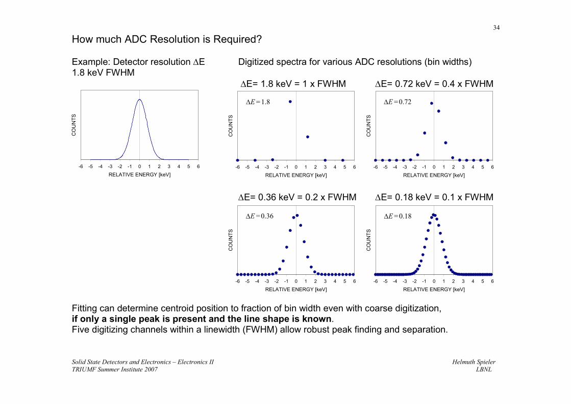
How much ADC Resolution is Required?
Example: Detector resolution ∆E Digitized spectra for various ADC resolutions (bin widths)1.8 keV FWHM
∆E= 1.8 keV = 1 x FWHM ∆E= 0.72 keV = 0.4 x FWHM
∆E= 0.36 keV = 0.2 x FWHM ∆E= 0.18 keV = 0.1 x FWHM
Fitting can determine centroid position to fraction of bin width even with coarse digitization,if only a single peak is present and the line shape is known.Five digitizing channels within a linewidth (FWHM) allow robust peak finding and separation.
-6 -5 -4 -3 -2 -1 0 1 2 3 4 5 6
RELATIVE ENERGY [keV]
CO
UN
TS
-6 -5 -4 -3 -2 -1 0 1 2 3 4 5 6
RELATIVE ENERGY [keV]
CO
UN
TS
∆E = 1.8
-6 -5 -4 -3 -2 -1 0 1 2 3 4 5 6
RELATIVE ENERGY [keV]
CO
UN
TS
∆E =0.72
-6 -5 -4 -3 -2 -1 0 1 2 3 4 5 6
RELATIVE ENERGY [keV]
CO
UN
TS
∆E =0.36
-6 -5 -4 -3 -2 -1 0 1 2 3 4 5 6
RELATIVE ENERGY [keV]
CO
UN
TS
∆E = 0.18

Solid State Detectors and Electronics – Electronics II Helmuth SpielerTRIUMF Summer Institute 2007 LBNL
35
2. Differential Non-Linearity
Differential non-linearity is a measure of the inequality of channel profiles over the range of the ADC.
Depending on the nature of the distribution, either a peak or an rms specification may be appropriate.
( ) ( )max 1 or r.m.s. 1
V i V iDNL DNL
V V
∆ ∆ = − = − ∆ ∆
where V∆ is the average channel width and ( )V i∆ is the width of an individual channel.
Typical differential non-linearity patterns (“white” input spectrum). vertical scale 10x larger than left↓
An ideal ADC would show an equal number of counts in each bin.The spectrum to the left shows a random pattern,but note the multiple periodicities visible in the right hand spectrum.
CHANNEL NUMBER CHANNEL NUMBER
CO
UN
TS
CO
UN
TS

Solid State Detectors and Electronics – Electronics II Helmuth SpielerTRIUMF Summer Institute 2007 LBNL
36
Differential non-linearity of < ±1% max. is typical, but state-of-the-art ADCs can achieve 10-3 rms,i.e. the variation is comparable to the statistical fluctuation for 106 random counts.
Note: Instrumentation ADCs are often specified with an accuracy of ±0.5 LSB (least significant bit) ormore, so
1. the differential non-linearity may be 50% or more,
2. the response may be non-monotonic
⇒ output may decrease when input rises.
Solid State Detectors and Electronics – Electronics II Helmuth SpielerTRIUMF Summer Institute 2007 LBNL
37
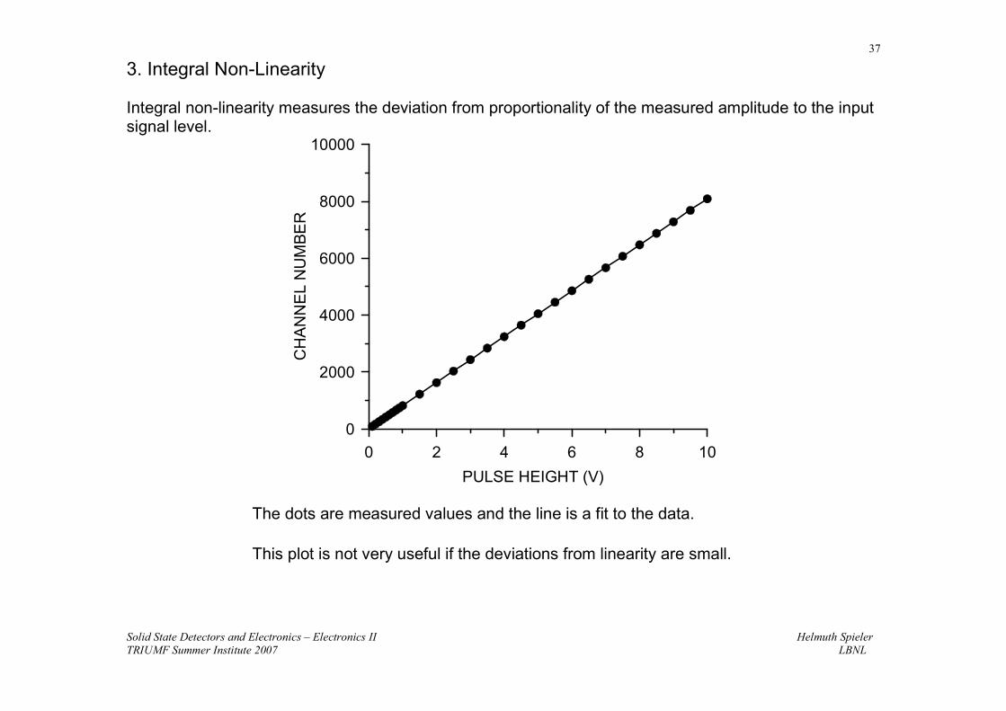
3. Integral Non-Linearity
Integral non-linearity measures the deviation from proportionality of the measured amplitude to the inputsignal level.
0 2 4 6 8 10PULSE HEIGHT (V)
0
2000
4000
6000
8000
10000
CH
AN
NE
LN
UM
BER
The dots are measured values and the line is a fit to the data.
This plot is not very useful if the deviations from linearity are small.

Solid State Detectors and Electronics – Electronics II Helmuth SpielerTRIUMF Summer Institute 2007 LBNL
38
Plotting the deviations of the measured pointsfrom the fit yields a more useful result.
Integral non-linearity measured with a400 ns wide input pulse
The linearity of an ADC can depend on theinput pulse shape and duration,due to bandwidth limitations in the circuitry.
Increasing the pulse width to 3 µs improvedthe linearity significantly:
0 2000 4000 6000 8000CHANNEL NUMBER
-20
-10
0
10
20
DE
VIA
TIO
NFR
OM
FIT
(ch)
0 2000 4000 6000 8000CHANNEL NUMBER
-2
-1
0
1
2
DE
VIA
TIO
NFR
OM
FIT
(ch)

Solid State Detectors and Electronics – Electronics II Helmuth SpielerTRIUMF Summer Institute 2007 LBNL
39
4. Conversion Time
During the acquisition of a signal the system cannot accept a subsequent signal (“dead time”)
Dead Time =
signal acquisition time → time-to-peak + const.
+ conversion time → can depend on pulse height
+ readout time to memory → depends on speed of data transmission and buffermemory access
Dead time affects measurements of yields or reaction cross-sections. Unless the event rate <<1/(dead time), it is necessary to measure the dead time, e.g. with a reference pulser fedsimultaneously into the spectrum.
The total number of reference pulses issued during the measurement is determined by a scalerand compared with the number of pulses recorded in the spectrum.
Does a pulse-height dependent dead time mean that the correction is a function of pulse height?
Usually not. If events in different part of the spectrum are not correlated in time, i.e. random, theyare all subject to the same average dead time (although this average will depend on the spectraldistribution).
• Caution with correlated events!Example: Decay chains, where lifetime is < dead time.
The daughter decay will be lost systematically.

Solid State Detectors and Electronics – Electronics II Helmuth SpielerTRIUMF Summer Institute 2007 LBNL
40
5. Count Rate Effects
Problems are usually due to internal baseline shifts with event rate or undershoots following a pulse.If signals occur at constant intervals, the effect of an undershoot will always be the same.However, in a random sequence of pulses, the effect will vary from pulse to pulse.
⇒ spectral broadening
Baseline shifts tend to manifest themselves as a systematic shift in centroid position with event rate.
Centroid shifts for two 13 bit ADCs vs. random rate:
0 40 80 120PULSE RATE (103 s-1)
-10
-8
-6
-4
-2
0
CE
NTR
OID
SH
IFT
(ch)

Solid State Detectors and Electronics – Electronics II Helmuth SpielerTRIUMF Summer Institute 2007 LBNL
41
6. Stability
Stability vs. temperature is usually adequate with modern electronics in a laboratory environment.
• Note that temperature changes within a module are typicallymuch smaller than ambient.
However: Highly precise or long-term measurements require spectrum stabilization tocompensate for changes in gain and baseline of the overall system.
Technique: Using precision pulsers place a reference peak at both the low and high end of thespectrum.
(Pk. Pos. 2) – (Pk. Pos. 1) → Gain, …
then
(Pk. Pos. 1) or (Pk. Pos. 2) → Offset
Traditional Implementation: Hardware,spectrum stabilizer module
Today, it is more convenient to determine the corrections in software.
These can be applied to calibration corrections or used to derive an electrical signal that is appliedto the hardware (simplest and best in the ADC).
Solid State Detectors and Electronics – Electronics II Helmuth SpielerTRIUMF Summer Institute 2007 LBNL
42
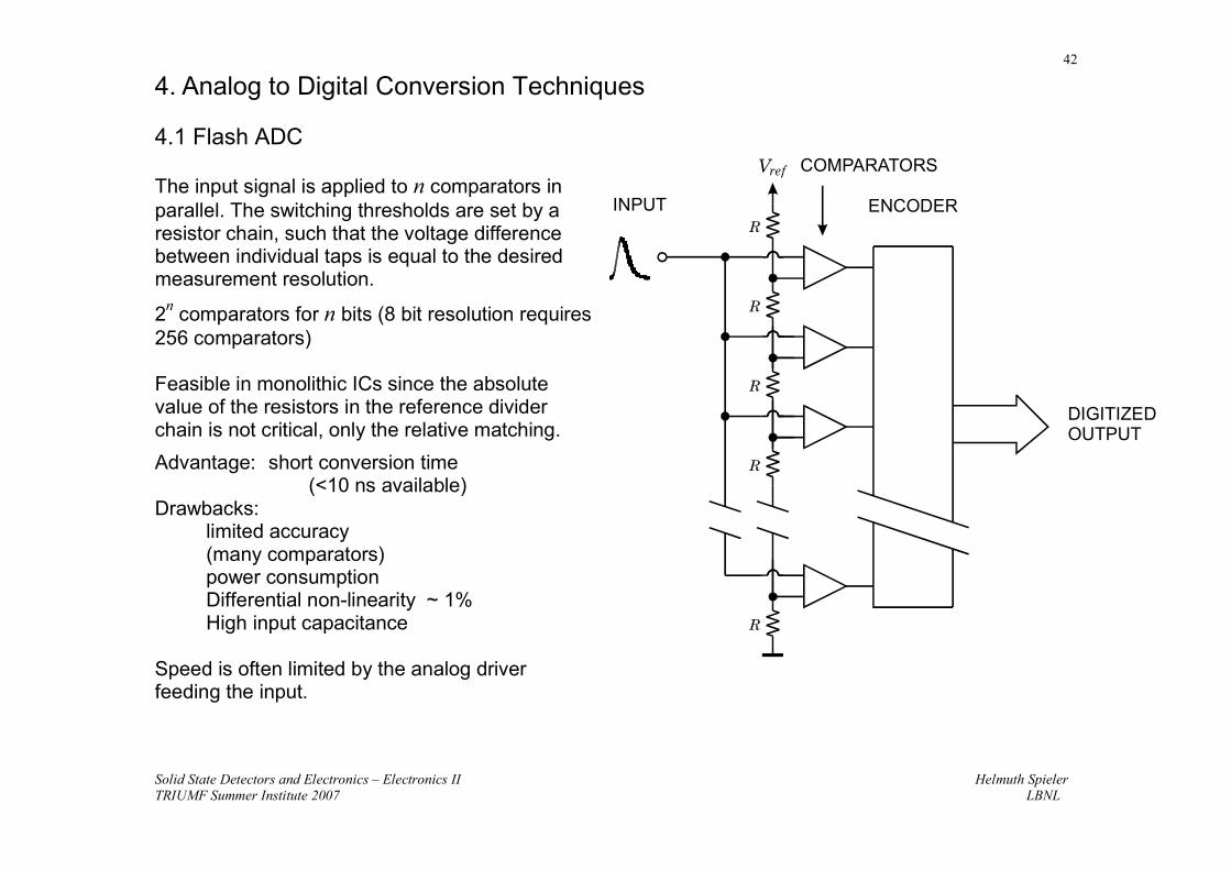
4. Analog to Digital Conversion Techniques
4.1 Flash ADC
The input signal is applied to n comparators inparallel. The switching thresholds are set by aresistor chain, such that the voltage differencebetween individual taps is equal to the desiredmeasurement resolution.
2n comparators for n bits (8 bit resolution requires256 comparators)
Feasible in monolithic ICs since the absolutevalue of the resistors in the reference dividerchain is not critical, only the relative matching.Advantage: short conversion time
(<10 ns available)Drawbacks:
limited accuracy(many comparators)power consumptionDifferential non-linearity ~ 1%High input capacitance
Speed is often limited by the analog driverfeeding the input.
Vref
R
R
R
R
R
DIGITIZEDOUTPUT
COMPARATORS
ENCODERINPUT

Solid State Detectors and Electronics – Electronics II Helmuth SpielerTRIUMF Summer Institute 2007 LBNL
43
4.2 Successive Approximation ADC
Sequentially raise comparatorthreshold proportional to2n, 2n-1, … 20 and setcorresponding bit if thecomparator output is high(DAC output < pulse height)
n conversion steps yield 2n
channels, i.e. 8K channelsrequire 13 steps
Advantages: speed (~ µs)high resolutionICs (monolithic + hybrid) available
Drawback: Differential non-linearity (typ. 10 – 20%)
Reason: Resistors that set DAC output must be extremely accurate. For DNL < 1%the resistor determining the 212 level in an 8K ADC must be accurate to < 2.4 . 10-6.
PULSESTRETCHER COMPARATOR CONTROL
LOGIC
DACADDRESS
DAC
DIGITIZEDOUTPUT
ANALOGINPUT

Solid State Detectors and Electronics – Electronics II Helmuth SpielerTRIUMF Summer Institute 2007 LBNL
44
DNL can be corrected by various techniques:
• averaging over many channel profiles for a given pulse amplitude (“sliding scale” or “Gattiprinciple”)
• correction DAC (“brute force” application of IC technology)
The primary DAC output is adjusted bythe output of a correction DAC to reducedifferential non-linearity.
Correction data are derived from ameasurement of DNL. Correctionsfor each bit are loaded into the RAM,which acts as a look-up table toprovide the appropriate value to thecorrection DAC for each bit of themain DAC.
The range of the correction DAC mustexceed the peak-to-peak differential non-linearity.
If the correction DAC has N bits, themaximum DNL is reduced by 1/2 (N-1)
(if deviations are symmetrical).
PULSESTRETCHER COMPARATOR CONTROL
LOGIC
DACADDRESS
LOAD CORRECTION DATA
SUMMINGAMPLIFIER
DAC
CORR.DAC RAM∆V= DNLP-P
DIGITIZEDOUTPUT
ANALOGINPUT

Solid State Detectors and Electronics – Electronics II Helmuth SpielerTRIUMF Summer Institute 2007 LBNL
45
4.3 Wilkinson ADC
The peak signal amplitude isacquired by a pulse stretcher andtransferred to a memorycapacitor.
Then, simultaneously,1. the capacitor is disconnected
from the stretcher,2. a current source is switched on
to linearly discharge thecapacitor,
3. a counter is enabled todetermine the number of clockpulses until the voltage on thecapacitor reaches thebaseline.
Advantage: excellent differential linearity (continuous conversion process)
Drawbacks: slow – conversion time = n . Tclock (n= channel number ∝ pulse height)Tclock= 10 ns → Tconv= 82 µs for 13 bits
Clock frequencies of 100 MHz typical,but >400 MHz possible with excellent performance
“Standard” technique for high-resolution spectroscopy.
PULSESTRETCHER COMPARATOR
DIGITIZEDOUTPUT
ANALOGINPUT
START STOP
V
I
V
BL
R
BL
COUNTERCLOCK
PEAKDETECTOROUTPUT

Solid State Detectors and Electronics – Electronics II Helmuth SpielerTRIUMF Summer Institute 2007 LBNL
46
4.4 Pipelined ADCs
Most common architecture for high-speedhigh-resolution ADCs
Input to each stage is fed both to a sample andhold (S&H) and a 3-bit flash ADC.
The S&H maintains the signal level duringconversion. The flash ADC quantizes its inputto 3 bit accuracy. This output is fed to a DACwith 12 bit accuracy. The DAC’s analog outputis subtracted from the original signal and thedifference signal is passed on to the nextstage.
The last 4 bits are resolved by a 4-bit flashADC.
As soon as a stage has passed its result to thenext stage it can begin processing the nextsignal, so throughput is not determined by the total conversion time, but by the time per stage.
Since the interstage gain is only 4 (rather than 8 corresponding to 3 bits), each stage only contributes 2bits of resolution. The extra bit is used for error correction.
Commercially available: 1 GS/s conversion rates with 8-bit resolution and a power dissipation of about1.5 W.
STAGE 1 STAGE 2 STAGE 3 STAGE 4
TIME ALIGNMENT
4-bitFLASHADC
3-bitFLASHADC
3-bitDAC
x4S&H ΣEACH STAGE
3 bits 3 bits 3 bits 3 bits 4 bits
12 bits

Solid State Detectors and Electronics – Electronics II Helmuth SpielerTRIUMF Summer Institute 2007 LBNL
47
Hybrid Analog-to-Digital Converters
Conversion techniques can be combined to obtain high resolution and short conversion time.
1. Flash + Successive Approximation orFlash + Wilkinson (Ramp Run-Down)
Utilize fast flash ADC for coarse conversion (e.g. 8 out of 13 bits)
Successive approximation or Wilkinson converter to provide fine resolution.Limited range, so short conversion time: 256 ch with 100 MHz clock ⇒ 2.6 µs
Results: 13 bit conversion in < 4 µs with excellent integral and differential linearity
2. Flash ADCs with Sub-Ranging
Not all applications require constant absolute resolution over the full range. Sometimes onlyrelative resolution must be maintained, especially in systems with a very large dynamic range.
Precision binary divider at input to determine coarse range + fast flash ADC for fine digitization.
Example: Fast digitizer that fits in phototube base (FNAL)
17 to 18 bit dynamic rangeDigital floating point output
(4 bit exponent, 8+1 bit mantissa)16 ns conversion time

Solid State Detectors and Electronics – Electronics II Helmuth SpielerTRIUMF Summer Institute 2007 LBNL
48
5. Time Digitizers
5.1 Counter
Simplest arrangement: Count clock pulses between start and stop.
Limitation: Speed of counterCurrent technology limits speed of counter system to about 1 GHz
⇒ ∆t = 1 ns
Advantages: SimplicityMulti-hit capability
DIGITIZEDOUTPUT
COUNTERCLOCK
QSSTART
STOP RSTART STOP

Solid State Detectors and Electronics – Electronics II Helmuth SpielerTRIUMF Summer Institute 2007 LBNL
49
5.2 Analog Ramp
Commonly used in high-resolutiondigitizers (∆t = 10 ps)
Principle:Charge capacitor through switchablecurrent source
Start pulse: turn on current sourceStop pulse: turn off current source
⇒ Voltage on storage capacitor
Use Wilkinson ADC with smallerdischarge current to digitize voltage.
Drawbacks: No multi-hit capability
Deadtime
Advantages: High resolution (~ps)
Excellent differential linearity
COMPARATOR
DIGITIZEDOUTPUT
V
I
I
V
BL
R
T
+
COUNTERCLOCK
START
STOP
C

Solid State Detectors and Electronics – Electronics II Helmuth SpielerTRIUMF Summer Institute 2007 LBNL
50
5.3 Digitizers with Clock Interpolation
Most experiments in HEP require multi-hit capability, no deadtimeCommonly used in HEP ICs for time digitization (Y. Arai, KEK)
D D D D D
CLK CLK CLK CLK CLK
Q Q Q Q Q
PHASECOMPARATOR
INPUT
REFERENCECLOCK
DIGITIZED OUTPUT TO MEMORY
Clock period interpolated by inverter delays (U1, U2, …).
Delay can be fine-tuned by adjusting operating point of inverters. Stabilized by delay locked loop.
Devices with 250 ps resolution fabricated and tested.
see Y. Arai et al., IEEE Trans. Nucl. Sci. NS-45/3 (1998) 735-739 and references therein.

Solid State Detectors and Electronics – Electronics II Helmuth SpielerTRIUMF Summer Institute 2007 LBNL
51
6. Digital Signal Processing
Sample detector signal with fast digitizer to reconstruct pulse:
Then use digital signal processor to perform mathematicaloperations for desired pulse shaping.
Block Diagram
DSP allows great flexibility in implementing filtering functions
However: increased circuit complexityincreased demands on ADC, compared to traditional shaping.
INCIDENTRADIATION PUBLICATION
DETECTOR PREAMP ADC DSP
0 10 20 30TIME (ns)
0.0
0.1
0.2
0.3
0.4
0.5
SIG
NA
L C
UR
RE
NT
(µA
)

Solid State Detectors and Electronics – Electronics II Helmuth SpielerTRIUMF Summer Institute 2007 LBNL
52
Important to choose sample interval sufficiently smallto capture pulse structure.
Sampling interval of 4 ns misses initial peak.
With too low a sampling rate high frequency componentswill be “aliased” to lower frequencies:
Applies to any form of sampling(time waveform, image, ...)
Nyquist condition:Sampling frequency > 2x highest signal frequency
SAMPLING TIMES
T T T T T T T1 2 3 4 5 6 7
ACTUALWAVEFORM
ALIASEDWAVEFORM
0 10 20 30TIME [ns]
0.0
0.2
0.4
0.6
SIG
NAL
CU
RR
ENT

Solid State Detectors and Electronics – Electronics II Helmuth SpielerTRIUMF Summer Institute 2007 LBNL
53
⇒ Fast ADC required + Pre-Filter to limit signal bandwidth
• Dynamic range requirements for ADC may be more severe than in analog filtered system (dependingon pulse shape and pre-filter).
• Digitization introduces additional noise (“quantization noise”)
If one bit corresponds to an amplitude interval ∆, the quantization noise/ 2 2 2
2
/ 2 12v
vdvσ
∆
−∆
∆= =
∆∫ .
(differential non-linearity introduces quasi-random noise)
• Electronics preceding ADC and front-end of ADC must exhibit same precision as analog system, i.e.baseline and other pulse-to-pulse amplitude fluctuations less than order Qn /10, i.e. typically 10-4 inhigh-resolution systems. For 10 V FS at the ADC input this corresponds to < 1 mV.
⇒ ADC must provide high performance at short conversion times. Today this is technically feasible forsome applications, e.g. detectors with moderate to long collection times (γ and x-ray detectors).
DETECTOR PREAMP ADC DSPPRE-FILTER

Solid State Detectors and Electronics – Electronics II Helmuth SpielerTRIUMF Summer Institute 2007 LBNL
54
Digital Filtering
Filtering is performed by convolution:
1
0
( ) ( ) ( )N
o ik
S n W k S n k−
=
= ⋅ −∑
( )W k is a set of coefficients that describes the weighting function yielding the desired pulse shape.
A filter performing this function is called a Finite Impulse Response (FIR) filter.
This is analogous to filtering in the frequency domain.
In the frequency domain the result of filtering is determined by multiplying the responses of the individualstages:
1 2( ) ( ) ( )G f G f G f= ⋅
where 1( )G f and 1( )G f are complex numbers.
The theory of Fourier transforms states that the equivalent result in the time domain is formed byconvolution of the individual time responses:
1 2 1 2( ) ( ) ( ) ( ) ( )g t g t g t g g t dτ τ τ+∞
−∞
= ∗ ≡ ⋅ −∫ ,
analogously to the discrete sum shown above.

Solid State Detectors and Electronics – Electronics II Helmuth SpielerTRIUMF Summer Institute 2007 LBNL
55
Benefits of digital signal processing:
• Flexibility in implementing filter functions
• Filters possible that are impractical in hardware
• Simple to change filter parameters
• Tail cancellation and pile-up rejection easily incorporated
• Adaptive filtering can be used to compensate for pulse shape variations.
Where is digital signal processing appropriate?
• Systems highly optimized forResolutionHigh counting rates
• Variable detector pulse shapes
Where is analog signal processing best (most efficient)?
• Fast shaping
• Systems not sensitive to pulse shape (fixed shaper constants)
• High density systems that require small circuit area or low power
Both types of systems require careful analog design.
Progress in fast ADCs (precision, reduced power) will expand range of DSP applications

Solid State Detectors and Electronics – Electronics II Helmuth SpielerTRIUMF Summer Institute 2007 LBNL
56
7. Readout Systems
Si strip detector
Inside a typical readout IC: 128 parallel channels of analog front-end electronicsLogic circuitry to decode control signals, load DACs, etc.Digital circuitry for zero-suppression, readout
PREAMPLIFIER SHAPER ANALOG PIPELINE ADC
ANALOG SIGNAL PROCESSING
ANALOG SIGNAL PROCESSING
ANALOG SIGNAL PROCESSING
ANALOG SIGNAL PROCESSING
ANALOG SIGNAL PROCESSING
TEST PULSE GENERATOR, DACs, R/ W POINTERS, etc.
SPARSIFICATION
DIGITALCONTROLOUTPUTDRIVERS
TOKEN IN
CONTROL
DATA OUT
TOKEN OUT

Solid State Detectors and Electronics – Electronics II Helmuth SpielerTRIUMF Summer Institute 2007 LBNL
57
Readout of multiple ICs
IC1 is designated as master.Readout is initiated by a trigger signal selecting appropriate time stamp to IC1.When all data from IC1 have been transferred, a token is passed to IC2When IC3 has finished, the token is passed back to IC1, which can begin a new cycle.
CONTROL BUS
DATA BUS
TOKENPASSING
STRIP DETECTOR
IC3 IC2 IC1

Solid State Detectors and Electronics – Electronics II Helmuth SpielerTRIUMF Summer Institute 2007 LBNL
58
ATLAS Silicon Strip system (SCT): ABCD chips mounted on hybrid

Solid State Detectors and Electronics – Electronics II Helmuth SpielerTRIUMF Summer Institute 2007 LBNL
59
ATLAS SCT Detector Module
HYBRID ASSEMBLYBeO FACINGS
SLOTTED WASHER
SILICON SENSORS
BASEBOARD TPGDATUM WASHER
BeO FACINGSCONNECTOR

Solid State Detectors and Electronics – Electronics II Helmuth SpielerTRIUMF Summer Institute 2007 LBNL
60
Solid State Detectors and Electronics – Electronics II Helmuth SpielerTRIUMF Summer Institute 2007 LBNL
61
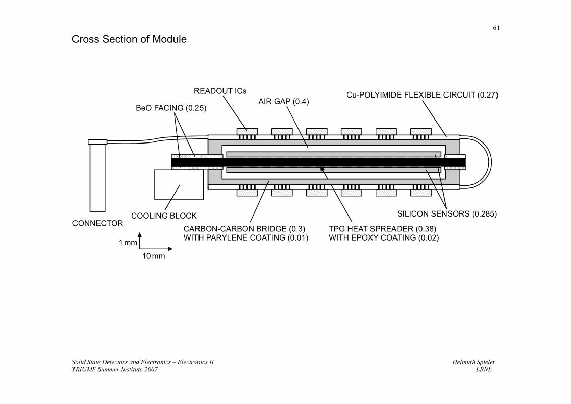
Cross Section of Module
READOUT ICs
BeO FACING (0.25)AIR GAP (0.4)
Cu-POLYIMIDE FLEXIBLE CIRCUIT (0.27)
SILICON SENSORS (0.285)
TPG HEAT SPREADER (0.38)WITH EPOXY COATING (0.02)
CARBON-CARBON BRIDGE (0.3)WITH PARYLENE COATING (0.01)
CONNECTORCOOLING BLOCK
10mm
1 mm

Solid State Detectors and Electronics – Electronics II Helmuth SpielerTRIUMF Summer Institute 2007 LBNL
62
TRACKINGDETECTORS
FRONT ENDELECTRONICS
LEVEL 1LATENCY15 sµ
READOUT
FRONT ENDELECTRONICS
READOUT
LVL1 TRIGGERPROCESSOR
CALORIMETER,OUTER TRACKER
LEVEL 2 TRIGGER FARM
LEVEL 3 TRIGGER FARM
DATA ARCHIVING
OFFDETECTOR
1.7 MHz
35 kHz
350 Hz
70 Hz
35 kHz VERTEXTRIGGER
Trigger Systems
Limiting rates:1. Detector Readout2. Archive rate
Requires compromises inintermediate steps, i.e.inefficiencies.
Example: CDF
Silicon detector still readout with Level 1trigger, but a dedicatedhardware vertex triggerutilizes ASICs andFPGAs to find displacedvertex events.
Improves rate of “good”events by factor 10 – 30.
FPGA computationaldensity roughly doublesper year.