Embed Size (px)
Citation preview

ELEN 350
Single Cycle Datapath
Adapted from the lecture notes of John Kubiatowicz(UCB)
and Hank Walker (TAMU)

The Big Picture: The Performance Perspective° Performance of a machine is determined by:
• Instruction count
• Clock cycle time
• Clock cycles per instruction
° Processor design (datapath and control) will determine:
• Clock cycle time
• Clock cycles per instruction
° Single cycle processor:
• Advantage: One clock cycle per instruction
• Disadvantage: long cycle time
CPI
Inst. Count Cycle Time

How to Design a Processor: step-by-step
° 1. Analyze instruction set => datapath requirements
• the meaning of each instruction is given by the register transfers
• datapath must include storage element for ISA registers
- possibly more
• datapath must support each register transfer
° 2. Select set of datapath components and establish clocking methodology
° 3. Assemble datapath meeting the requirements
° 4. Analyze implementation of each instruction to determine setting of control points that effects the register transfer.
° 5. Assemble the control logic

The MIPS Instruction Formats
° All MIPS instructions are 32 bits long. The three instruction formats:
• R-type
• I-type
• J-type
° The different fields are:
• op: operation of the instruction
• rs, rt, rd: the source and destination register specifiers
• shamt: shift amount
• funct: selects the variant of the operation in the “op” field
• address / immediate: address offset or immediate value
• target address: target address of the jump instruction
op target address
02631
6 bits 26 bits
op rs rt rd shamt funct
061116212631
6 bits 6 bits5 bits5 bits5 bits5 bits
op rs rt immediate
016212631
6 bits 16 bits5 bits5 bits

Step 1a: The MIPS-lite Subset
° ADD and SUB
• addu rd, rs, rt
• subu rd, rs, rt
° OR Immediate:
• ori rt, rs, imm16
° LOAD and STORE Word
• lw rt, rs, imm16
• sw rt, rs, imm16
° BRANCH:
• beq rs, rt, imm16
op rs rt rd shamt funct
061116212631
6 bits 6 bits5 bits5 bits5 bits5 bits
op rs rt immediate
016212631
6 bits 16 bits5 bits5 bits
op rs rt immediate
016212631
6 bits 16 bits5 bits5 bits
op rs rt immediate
016212631
6 bits 16 bits5 bits5 bits

Logical Register Transfers
° RTL gives the meaning of the instructions
° All start by fetching the instructionop | rs | rt | rd | shamt | funct = MEM[ PC ]
op | rs | rt | Imm16 = MEM[ PC ]
inst Register Transfers
addu R[rd] <– R[rs] + R[rt]; PC <– PC + 4
subu R[rd] <– R[rs] – R[rt]; PC <– PC + 4
ori R[rt] <– R[rs] | zero_ext(Imm16); PC <– PC + 4
lw R[rt] <– MEM[ R[rs] + sign_ext(Imm16)]; PC <– PC + 4
sw MEM[ R[rs] + sign_ext(Imm16) ] <– R[rt]; PC <– PC + 4
beq if ( R[rs] == R[rt] ) then PC <– PC + 4 +sign_ext(Imm16)] || 00
else PC <– PC + 4

Step 1: Requirements of the Instruction Set
° Memory
• instruction & data
° Registers (32 x 32)
• read RS
• read RT
• Write RT or RD
° PC
° Extender
° Add and Sub register or extended immediate
° Add 4 or extended immediate to PC

Step 2: Components of the Datapath
° Combinational Elements
° Storage Elements• Clocking methodology

Combinational Logic Elements (Basic Building Blocks)
° Adder
° MUX
° ALU
32
32
A
B32
Sum
Carry
32
32
A
B32
Result
OP
32A
B32
Y32
Select
Ad
der
MU
XA
LU
CarryIn

Verilog Implementation of Basic Blocks
module adder(sum, carry_out, a, b, carry_in); input [31:0] a, b;
input carry_in;output [31:0] sum;output carry_out;
assign {carry_out, sum} = a+b; endmodule
module mux(y, a, b, select);input [31:0] a, b;input select;output [31:0] y;
assign y = (select) ? a: b;
endmodule
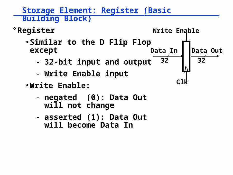
Storage Element: Register (Basic Building Block)
° Register
• Similar to the D Flip Flop except
- 32-bit input and output
- Write Enable input
• Write Enable:
- negated (0): Data Out will not change
- asserted (1): Data Out will become Data In
Clk
Data In
Write Enable
32 32
Data Out
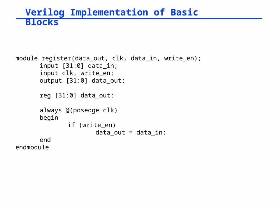
Verilog Implementation of Basic Blocks
module register(data_out, clk, data_in, write_en); input [31:0] data_in;
input clk, write_en;output [31:0] data_out;
reg [31:0] data_out;
always @(posedge clk)begin
if (write_en)data_out = data_in;
end endmodule

Storage Element: Register File
° Register File consists of 32 registers:
• Two 32-bit output busses:
busA and busB
• One 32-bit input bus: busW
° Register is selected by:
• RA (number) selects the register to put on busA (data)
• RB (number) selects the register to put on busB (data)
• RW (number) selects the register to be writtenvia busW (data) when Write Enable is 1
° Clock input (CLK)
• The CLK input is a factor ONLY during write operation
• During read operation, behaves as a combinational logic block:
- RA or RB valid => busA or busB valid after “access time.”
Clk
busW
Write Enable
3232
busA
32busB
5 5 5RWRA RB
32 32-bitRegisters

Storage Element: Idealized Memory
° Memory (idealized)
• One input bus: Data In
• One output bus: Data Out
° Memory word is selected by:
• Address selects the word to put on Data Out
• Write Enable = 1: address selects the memoryword to be written via the Data In bus
° Clock input (CLK)
• The CLK input is a factor ONLY during write operation
• During read operation, behaves as a combinational logic block:
- Address valid => Data Out valid after “access time.”
Clk
Data In
Write Enable
32 32DataOut
Address

Clocking Methodology (Simple View)
° All storage elements are clocked by the same clock edge
° CLK-to-Q + Longest Delay Path < Cycle Time
° What is the longest path?
Clk
.
.
.
.
.
.
.
.
.
.
.
.
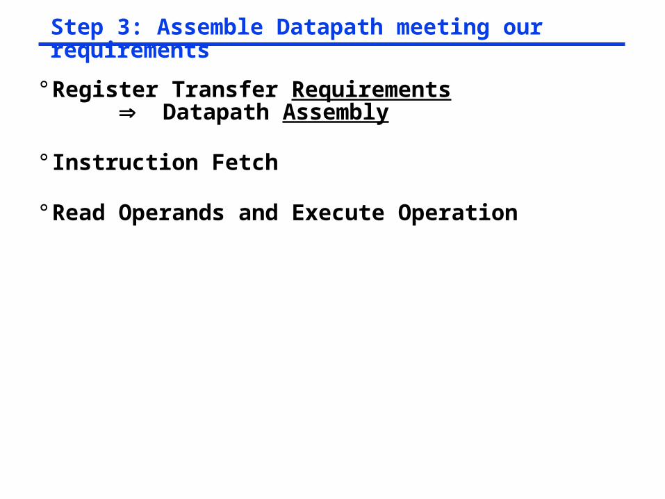
Step 3: Assemble Datapath meeting our requirements
° Register Transfer Requirements Datapath Assembly
° Instruction Fetch
° Read Operands and Execute Operation

3a: Overview of the Instruction Fetch Unit
° The common RTL operations
• Fetch the Instruction: mem[PC]
• Update the program counter:
- Sequential Code: PC <- PC + 4
- Branch and Jump: PC <- “something else”
32
Instruction WordAddress
InstructionMemory
PCClk
Next AddressLogic
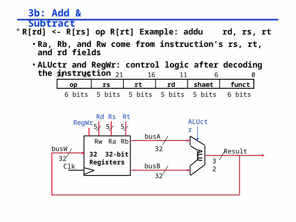
3b: Add & Subtract
° R[rd] <- R[rs] op R[rt] Example: addu rd, rs, rt
• Ra, Rb, and Rw come from instruction’s rs, rt, and rd fields
• ALUctr and RegWr: control logic after decoding the instruction
32
Result
ALUctr
Clk
busW
RegWr
32
32
busA
32
busB
5 5 5
Rw Ra Rb
32 32-bitRegisters
Rs RtRd
AL
U
op rs rt rd shamt funct
061116212631
6 bits 6 bits5 bits5 bits5 bits5 bits

Register-Register Timing: One complete cycle
32Result
ALUctr
Clk
busW
RegWr
3232
busA
32busB
5 5 5
Rw Ra Rb
32 32-bitRegisters
Rs RtRd
AL
U
Clk
PC
Rs, Rt, Rd,Op, Func
Clk-to-Q
ALUctr
Instruction Memory Access Time
Old Value New Value
RegWr Old Value New Value
Delay through Control Logic
busA, BRegister File Access Time
Old Value New Value
busW
ALU Delay
Old Value New Value
Old Value New Value
New ValueOld Value
Register WriteOccurs Here
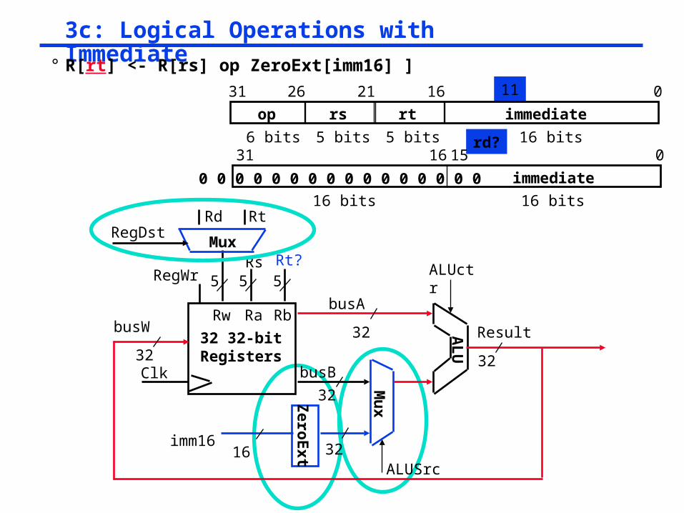
3c: Logical Operations with Immediate° R[rt] <- R[rs] op ZeroExt[imm16] ]
32
Result
ALUctr
Clk
busW
RegWr
32
32
busA
32
busB
5 5 5
Rw Ra Rb
32 32-bitRegisters
Rs
ZeroE
xt
Mu
x
RtRdRegDst
Mux
3216imm16
ALUSrc
AL
U
11
op rs rt immediate
016212631
6 bits 16 bits5 bits5 bits rd?
immediate
016 1531
16 bits16 bits
0 0 0 0 0 0 0 0 0 0 0 0 0 0 0 0
Rt?
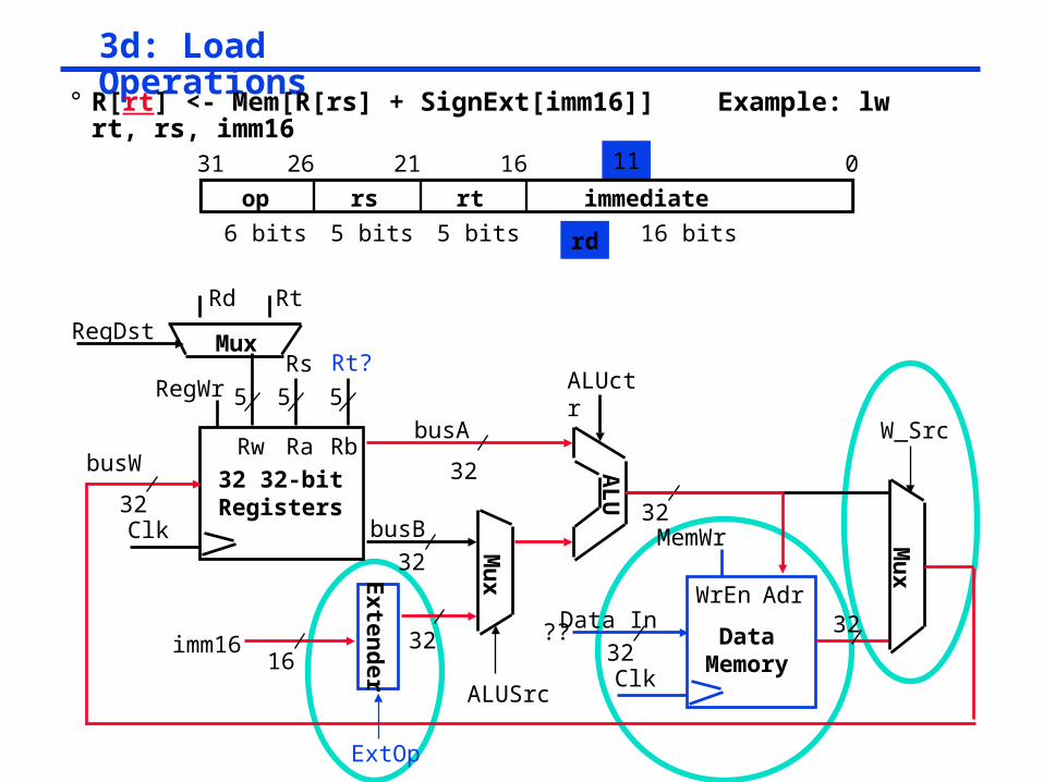
3d: Load Operations
° R[rt] <- Mem[R[rs] + SignExt[imm16]] Example: lw rt, rs, imm16
11
op rs rt immediate
016212631
6 bits 16 bits5 bits5 bits rd
32
ALUctr
Clk
busW
RegWr
32
32
busA
32
busB
5 5 5
Rw Ra Rb
32 32-bitRegisters
Rs
RtRd
RegDst
Exten
der
Mu
x
Mux
3216
imm16
ALUSrc
ExtOp
Clk
Data InWrEn
32
Adr
DataMemory
32
AL
U
MemWr Mu
x
W_Src
??
Rt?

3e: Store Operations
° Mem[ R[rs] + SignExt[imm16] <- R[rt] ] Example: sw rt, rs, imm16
op rs rt immediate
016212631
6 bits 16 bits5 bits5 bits
32
ALUctr
Clk
busW
RegWr
32
32
busA
32
busB
55 5
Rw Ra Rb
32 32-bitRegisters
Rs
Rt
Rt
Rd
RegDst
Exten
der
Mu
x
Mux
3216imm16
ALUSrcExtOp
Clk
Data InWrEn
32
Adr
DataMemory
MemWr
AL
U
32
Mu
x
W_Src
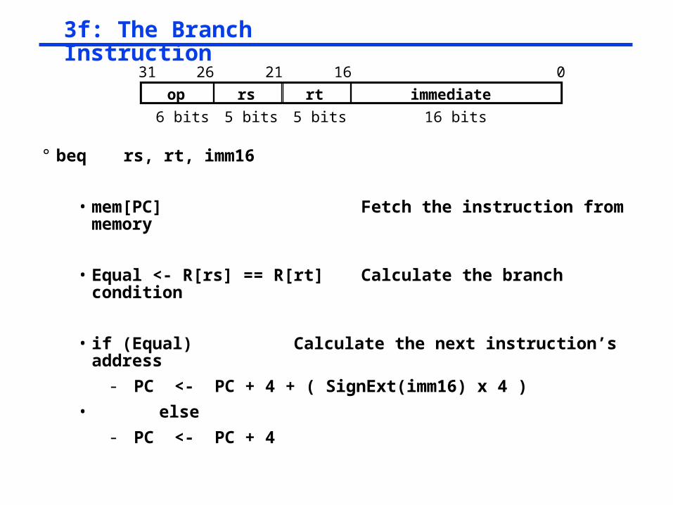
3f: The Branch Instruction
° beq rs, rt, imm16
• mem[PC] Fetch the instruction from memory
• Equal <- R[rs] == R[rt] Calculate the branch condition
• if (Equal) Calculate the next instruction’s address
- PC <- PC + 4 + ( SignExt(imm16) x 4 )
• else
- PC <- PC + 4
op rs rt immediate
016212631
6 bits 16 bits5 bits5 bits

Datapath for Branch Operations
° beq rs, rt, imm16 Datapath generates condition (equal)
op rs rt immediate
016212631
6 bits 16 bits5 bits5 bits
32
imm16
PC
Clk
00
Ad
der
Mu
x
Ad
der
4nPC_sel
Clk
busW
RegWr
32
busA
32
busB
5 5 5
Rw Ra Rb
32 32-bitRegisters
Rs Rt
Eq
ual
?
Cond
PC
Ext
Inst Address

Putting it All Together: A Single Cycle Datapath
imm
16
32
ALUctr
Clk
busW
RegWr
32
32
busA
32
busB
55 5
Rw Ra Rb
32 32-bitRegisters
Rs
Rt
Rt
RdRegDst
Exten
der
Mu
x
3216imm16
ALUSrcExtOp
Mu
x
MemtoReg
Clk
Data InWrEn32 Adr
DataMemory
MemWrA
LU
Equal
Instruction<31:0>
0
1
0
1
01
<21:25>
<16:20>
<11:15>
<0:15>
Imm16RdRtRs
=
Ad
der
Ad
der
PC
Clk
00
Mu
x
4
nPC_sel
PC
Ext
Adr
InstMemory

An Abstract View of the Critical Path° Register file and ideal memory:
• The CLK input is a factor ONLY during write operation
• During read operation, behave as combinational logic:
- Address valid => Output valid after “access time.”
Critical Path (Load Operation) = PC’s Clk-to-Q + Instruction Memory’s Access Time + Register File’s Access Time + ALU to Perform a 32-bit Add + Data Memory Access Time + Setup Time for Register File Write + Clock Skew
Clk
5
Rw Ra Rb
32 32-bitRegisters
RdA
LU
Clk
Data In
DataAddress
IdealData
Memory
Instruction
InstructionAddress
IdealInstruction
Memory
Clk
PC
5Rs
5Rt
16Imm
32
323232
A
B
Nex
t A
dd
ress

An Abstract View of the Implementation
DataOut
Clk
5
Rw Ra Rb
32 32-bitRegisters
Rd
AL
U
Clk
Data In
DataAddress
IdealData
Memory
Instruction
InstructionAddress
IdealInstruction
Memory
Clk
PC
5Rs
5Rt
32
323232
A
B
Nex
t A
dd
ress
Control
Datapath
Control Signals Conditions

Recap: A Single Cycle Datapath
° Rs, Rt, Rd and Imed16 hardwired into datapath from Fetch Unit° We have everything except control signals (underline)
• Today’s lecture will show you how to generate the control signals
32
ALUctr
Clk
busW
RegWr
32
32
busA
32
busB
55 5
Rw Ra Rb
32 32-bitRegisters
Rs
Rt
Rt
Rd
RegDst
Exten
der
Mu
x
Mux
3216imm16
ALUSrc
ExtOp
Mu
x
MemtoReg
Clk
Data InWrEn
32
Adr
DataMemory
32
MemWrA
LU
InstructionFetch Unit
Clk
Zero
Instruction<31:0>
0
1
0
1
01<
21:25>
<16:20>
<11:15>
<0:15>
Imm16RdRsRt
nPC_sel

Recap: Meaning of the Control Signals
° nPC_MUX_sel: 0 PC <– PC + 4 1 PC <– PC + 4 + SignExt(Im16) || 00
° Later in lecture: higher-level connection between mux and branch cond
Adr
InstMemory
Ad
der
Ad
der
PC
Clk
00
Mu
x
4
nPC_MUX_sel
PC
Extim
m16

Recap: Meaning of the Control Signals° ExtOp: “zero”, “sign”
° ALUsrc: 0 regB; 1 immed
° ALUctr: “add”, “sub”, “or”
° MemWr: 1 write memory
° MemtoReg: 0 ALU; 1 Mem
° RegDst: 0 “rt”; 1 “rd”
° RegWr: 1 write register
32
ALUctr
Clk
busW
RegWr
3232
busA
32
busB
55 5
Rw Ra Rb
32 32-bitRegisters
Rs
Rt
Rt
RdRegDst
Exten
der
Mu
x
3216imm16
ALUSrcExtOp
Mu
x
MemtoReg
Clk
Data InWrEn32 Adr
DataMemory
MemWr
AL
U
Equal
0
1
0
1
01
=

RTL: The Add Instruction
° add rd, rs, rt
• mem[PC] Fetch the instruction from memory
• R[rd] <- R[rs] + R[rt] The actual operation
• PC <- PC + 4 Calculate the next instruction’s address
op rs rt rd shamt funct
061116212631
6 bits 6 bits5 bits5 bits5 bits5 bits

Instruction Fetch Unit at the Beginning of Add
° Fetch the instruction from Instruction memory: Instruction <- mem[PC]
• This is the same for all instructions
PC
Ext
Adr
InstMemory
Ad
der
Ad
der
PC
Clk
00
Mu
x
4
nPC_MUX_sel
imm
16Instruction<31:0>

The Single Cycle Datapath during Add
32
ALUctr = Add
Clk
busW
RegWr = 1
32
32
busA
32
busB
55 5
Rw Ra Rb
32 32-bitRegisters
Rs
Rt
Rt
RdRegDst = 1
Exten
der
Mu
x
Mux
3216imm16
ALUSrc = 0
ExtOp = x
Mu
x
MemtoReg = 0
Clk
Data InWrEn
32
Adr
DataMemory
32
MemWr = 0A
LU
InstructionFetch Unit
Clk
Zero
Instruction<31:0>° R[rd] <- R[rs] + R[rt]
0
1
0
1
01<
21:25>
<16:20>
<11:15>
<0:15>
Imm16RdRsRt
op rs rt rd shamt funct
061116212631
nPC_sel= +4

Clk
Instruction Fetch Unit at the End of Add
° PC <- PC + 4
• This is the same for all instructions except: Branch and Jump
Adr
InstMemory
Ad
der
Ad
der
PC
00
Mu
x
4
nPC_MUX_sel
imm
16Instruction<31:0>
0
1
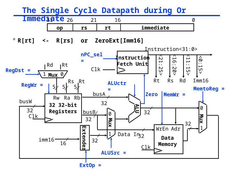
The Single Cycle Datapath during Or Immediate
° R[rt] <- R[rs] or ZeroExt[Imm16]
op rs rt immediate
016212631
32
ALUctr =
Clk
busW
RegWr =
32
32
busA
32
busB
55 5
Rw Ra Rb
32 32-bitRegisters
Rs
Rt
Rt
RdRegDst =
Exten
der
Mu
x
Mux
3216imm16
ALUSrc =
ExtOp =
Mu
x
MemtoReg =
Clk
Data InWrEn
32
Adr
DataMemory
32
MemWr = A
LU
InstructionFetch Unit
Clk
Zero
Instruction<31:0>
0
1
0
1
01<
21:25>
<16:20>
<11:15>
<0:15>
Imm16RdRsRt
nPC_sel =

The Single Cycle Datapath during Load
32
ALUctr = Add
Clk
busW
RegWr = 1
32
32
busA
32
busB
55 5
Rw Ra Rb
32 32-bitRegisters
Rs
Rt
Rt
RdRegDst = 0
Exten
der
Mu
x
Mux
3216imm16
ALUSrc = 1
ExtOp = 1
Mu
x
MemtoReg = 1
Clk
Data InWrEn
32
Adr
DataMemory
32
MemWr = 0A
LU
InstructionFetch Unit
Clk
Zero
Instruction<31:0>
0
1
0
1
01<
21:25>
<16:20>
<11:15>
<0:15>
Imm16RdRsRt
° R[rt] <- Data Memory {R[rs] + SignExt[imm16]}
op rs rt immediate
016212631
nPC_sel= +4

The Single Cycle Datapath during Store
° Data Memory {R[rs] + SignExt[imm16]} <- R[rt]
op rs rt immediate
016212631
32
ALUctr =
Clk
busW
RegWr =
32
32
busA
32
busB
55 5
Rw Ra Rb
32 32-bitRegisters
Rs
Rt
Rt
RdRegDst =
Exten
der
Mu
x
Mux
3216imm16
ALUSrc =
ExtOp =
Mu
x
MemtoReg =
Clk
Data InWrEn
32
Adr
DataMemory
32
MemWr = A
LU
InstructionFetch Unit
Clk
Zero
Instruction<31:0>
0
1
0
1
01<
21:25>
<16:20>
<11:15>
<0:15>
Imm16RdRsRt
nPC_sel =
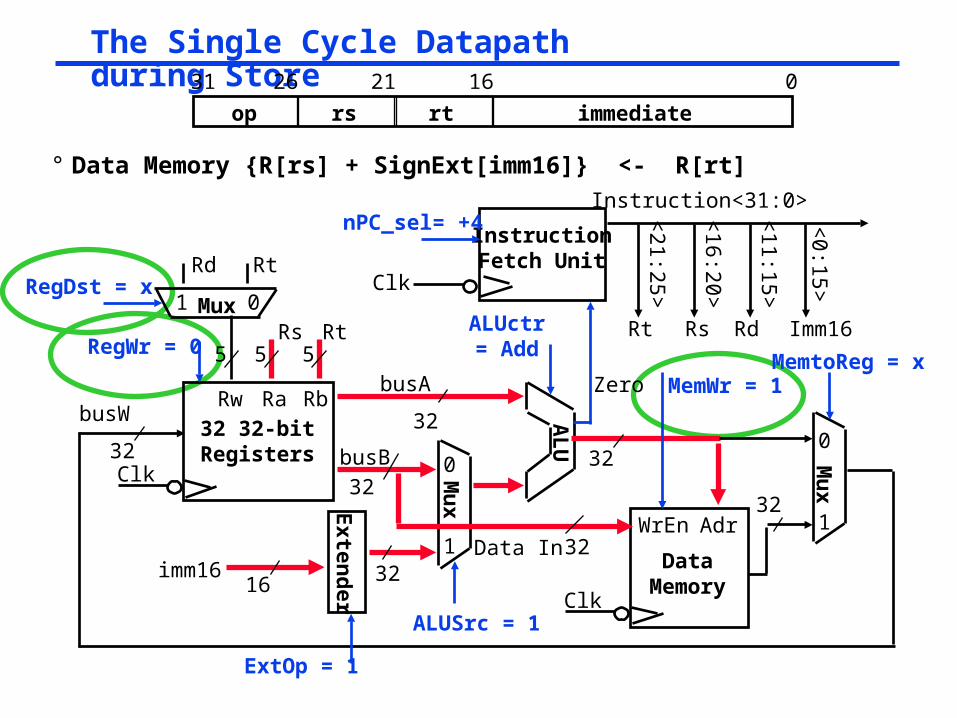
The Single Cycle Datapath during Store
32
ALUctr = Add
Clk
busW
RegWr = 0
32
32
busA
32
busB
55 5
Rw Ra Rb
32 32-bitRegisters
Rs
Rt
Rt
RdRegDst = x
Exten
der
Mu
x
Mux
3216imm16
ALUSrc = 1
ExtOp = 1
Mu
x
MemtoReg = x
Clk
Data InWrEn
32Adr
DataMemory
32
MemWr = 1A
LU
InstructionFetch Unit
Clk
Zero
Instruction<31:0>
0
1
0
1
01<
21:25>
<16:20>
<11:15>
<0:15>
Imm16RdRsRt
° Data Memory {R[rs] + SignExt[imm16]} <- R[rt]
op rs rt immediate
016212631
nPC_sel= +4

The Single Cycle Datapath during Branch
32
ALUctr =Sub
Clk
busW
RegWr = 0
32
32
busA
32
busB
55 5
Rw Ra Rb
32 32-bitRegisters
Rs
Rt
Rt
RdRegDst = x
Exten
der
Mu
x
Mux
3216imm16
ALUSrc = 0
ExtOp = x
Mu
x
MemtoReg = x
Clk
Data InWrEn
32
Adr
DataMemory
32
MemWr = 0A
LU
InstructionFetch Unit
Clk
Zero
Instruction<31:0>
0
1
0
1
01<
21:25>
<16:20>
<11:15>
<0:15>
Imm16RdRsRt
° if (R[rs] - R[rt] == 0) then Zero <- 1 ; else Zero <- 0
op rs rt immediate
016212631
nPC_sel= “Br”

Instruction Fetch Unit at the End of Branch
° if (Zero == 1) then PC = PC + 4 + SignExt[imm16]*4 ; else PC = PC + 4
op rs rt immediate
016212631
° What is encoding of nPC_sel?
• Direct MUX select?
• Branch / not branch
° Let’s choose second option
nPC_sel zero? MUX0 x 01 0 01 1 1
Adr
InstMemory
Ad
der
Ad
der
PC
Clk
00
Mu
x
4
nPC_sel
imm
16
Instruction<31:0>
0
1
Zero
nPC_MUX_sel
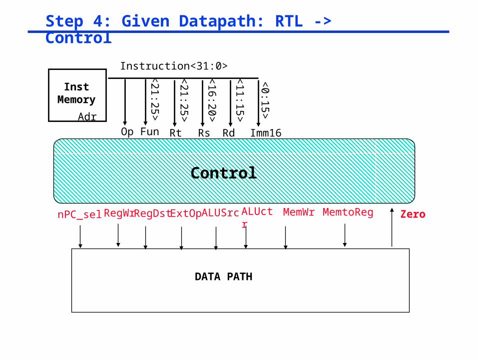
Step 4: Given Datapath: RTL -> Control
ALUctrRegDst ALUSrcExtOp MemtoRegMemWr Zero
Instruction<31:0>
<21:25>
<16:20>
<11:15>
<0:15>
Imm16RdRsRt
nPC_sel
Adr
InstMemory
DATA PATH
Control
Op
<21:25>
Fun
RegWr

A Summary of Control Signals
inst Register Transfer
ADD R[rd] <– R[rs] + R[rt]; PC <– PC + 4
ALUsrc = RegB, ALUctr = “add”, RegDst = rd, RegWr, nPC_sel = “+4”
SUB R[rd] <– R[rs] – R[rt]; PC <– PC + 4
ALUsrc = RegB, ALUctr = “sub”, RegDst = rd, RegWr, nPC_sel = “+4”
ORi R[rt] <– R[rs] + zero_ext(Imm16); PC <– PC + 4
ALUsrc = Im, Extop = “Z”, ALUctr = “or”, RegDst = rt, RegWr, nPC_sel = “+4”
LOAD R[rt] <– MEM[ R[rs] + sign_ext(Imm16)]; PC <– PC + 4
ALUsrc = Im, Extop = “Sn”, ALUctr = “add”, MemtoReg, RegDst = rt, RegWr, nPC_sel = “+4”
STORE MEM[ R[rs] + sign_ext(Imm16)] <– R[rs]; PC <– PC + 4
ALUsrc = Im, Extop = “Sn”, ALUctr = “add”, MemWr, nPC_sel = “+4”
BEQ if ( R[rs] == R[rt] ) then PC <– PC + sign_ext(Imm16)] || 00 else PC <– PC + 4
nPC_sel = “Br”, ALUctr = “sub”

A Summary of the Control Signals
add sub ori lw sw beq jump
RegDst
ALUSrc
MemtoReg
RegWrite
MemWrite
nPCsel
Jump
ExtOp
ALUctr<2:0>
1
0
0
1
0
0
0
x
Add
1
0
0
1
0
0
0
x
Subtract
0
1
0
1
0
0
0
0
Or
0
1
1
1
0
0
0
1
Add
x
1
x
0
1
0
0
1
Add
x
0
x
0
0
1
0
x
Subtract
x
x
x
0
0
0
1
x
xxx
op target address
op rs rt rd shamt funct
061116212631
op rs rt immediate
R-type
I-type
J-type
add, sub
ori, lw, sw, beq
jump
func
op 000000 000000 001101 100011 101011 000100 000010Appendix A100000See 100010 We Don’t Care :-)

The Concept of Local Decoding
R-type ori lw sw beq jump
RegDst
ALUSrc
MemtoReg
RegWrite
MemWrite
Branch
Jump
ExtOp
ALUop<N:0>
1
0
0
1
0
0
0
x
“R-type”
0
1
0
1
0
0
0
0
Or
0
1
1
1
0
0
0
1
Add
x
1
x
0
1
0
0
1
Add
x
0
x
0
0
1
0
x
Subtract
x
x
x
0
0
0
1
x
xxx
op 00 0000 00 1101 10 0011 10 1011 00 0100 00 0010
MainControl
op
6
ALUControl(Local)
func
N
6ALUop
ALUctr
3
AL
U

The Encoding of ALUop
° In this exercise, ALUop has to be 2 bits wide to represent:
• (1) “R-type” instructions
• “I-type” instructions that require the ALU to perform:
- (2) Or, (3) Add, and (4) Subtract
° To implement the full MIPS ISA, ALUop has to be 3 bits to represent:
• (1) “R-type” instructions
• “I-type” instructions that require the ALU to perform:
- (2) Or, (3) Add, (4) Subtract, and (5) And (Example: andi)
MainControl
op
6
ALUControl(Local)
func
N
6ALUop
ALUctr
3
R-type ori lw sw beq jump
ALUop (Symbolic) “R-type” Or Add Add Subtract xxx
ALUop<2:0> 1 00 0 10 0 00 0 00 0 01 xxx
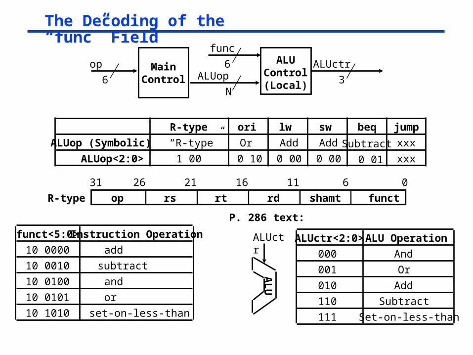
The Decoding of the “func” Field
R-type ori lw sw beq jump
ALUop (Symbolic) “R-type” Or Add Add Subtract xxx
ALUop<2:0> 1 00 0 10 0 00 0 00 0 01 xxx
MainControl
op
6
ALUControl(Local)
func
N
6ALUop
ALUctr
3
op rs rt rd shamt funct
061116212631
R-type
funct<5:0> Instruction Operation
10 0000
10 0010
10 0100
10 0101
10 1010
add
subtract
and
or
set-on-less-than
ALUctr<2:0> ALU Operation
000
001
010
110
111
And
Or
Add
Subtract
Set-on-less-than
P. 286 text:
ALUctr
AL
U

The Truth Table for ALUctr
R-type ori lw sw beqALUop(Symbolic) “R-type” Or Add Add Subtract
ALUop<2:0> 1 00 0 10 0 00 0 00 0 01
ALUop func
bit<2> bit<1> bit<0> bit<2> bit<1> bit<0>bit<3>
0 0 0 x x x x
ALUctrALUOperation
Add 0 1 0
bit<2> bit<1> bit<0>
0 x 1 x x x x Subtract 1 1 0
0 1 x x x x x Or 0 0 1
1 x x 0 0 0 0 Add 0 1 0
1 x x 0 0 1 0 Subtract 1 1 0
1 x x 0 1 0 0 And 0 0 0
1 x x 0 1 0 1 Or 0 0 1
1 x x 1 0 1 0 Set on < 1 1 1
funct<3:0> Instruction Op.
0000
0010
0100
0101
1010
add
subtract
and
or
set-on-less-than
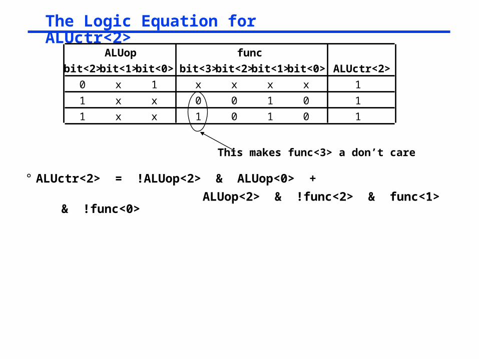
The Logic Equation for ALUctr<2>
ALUop func
bit<2> bit<1> bit<0> bit<2> bit<1> bit<0>bit<3> ALUctr<2>
0 x 1 x x x x 1
1 x x 0 0 1 0 1
1 x x 1 0 1 0 1
° ALUctr<2> = !ALUop<2> & ALUop<0> +
ALUop<2> & !func<2> & func<1> & !func<0>
This makes func<3> a don’t care

The Logic Equation for ALUctr<1>
ALUop func
bit<2> bit<1> bit<0> bit<2> bit<1> bit<0>bit<3>
0 0 0 x x x x 1
ALUctr<1>
0 x 1 x x x x 1
1 x x 0 0 0 0 1
1 x x 0 0 1 0 1
1 x x 1 0 1 0 1
° ALUctr<1> = !ALUop<2> & !ALUop<1> +
ALUop<2> & !func<2> & !func<0>

The Logic Equation for ALUctr<0>
ALUop func
bit<2> bit<1> bit<0> bit<2> bit<1> bit<0>bit<3> ALUctr<0>
0 1 x x x x x 1
1 x x 0 1 0 1 1
1 x x 1 0 1 0 1
° ALUctr<0> = !ALUop<2> & ALUop<1>
+ ALUop<2> & !func<3> & func<2> & !func<1> & func<0>
+ ALUop<2> & func<3> & !func<2> & func<1> & !func<0>

The ALU Control Block
ALUControl(Local)
func
3
6ALUop
ALUctr
3
° ALUctr<2> = !ALUop<2> & ALUop<0> +
ALUop<2> & !func<2> & func<1> & !func<0>
° ALUctr<1> = !ALUop<2> & !ALUop<1> +
ALUop<2> & !func<2> & !func<0>
° ALUctr<0> = !ALUop<2> & ALUop<1>
+ ALUop<2> & !func<3> & func<2> & !func<1> & func<0>
+ ALUop<2> & func<3> & !func<2> & func<1> & !func<0>
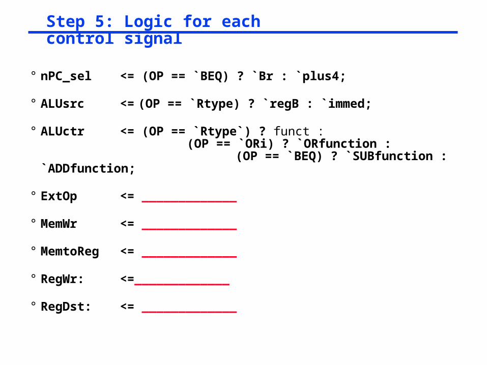
Step 5: Logic for each control signal
° nPC_sel <= (OP == `BEQ) ? `Br : `plus4;
° ALUsrc <= (OP == `Rtype) ? `regB : `immed;
° ALUctr <= (OP == `Rtype`) ? funct :(OP == `ORi) ? `ORfunction :(OP == `BEQ) ? `SUBfunction : `ADDfunction;
° ExtOp <= _____________
° MemWr <= _____________
° MemtoReg <= _____________
° RegWr: <=_____________
° RegDst: <= _____________

Step 5: Logic for each control signal
° nPC_sel <= (OP == `BEQ) ? `Br : `plus4;
° ALUsrc <= (OP == `Rtype) ? `regB : `immed;
° ALUctr <= (OP == `Rtype`) ? funct :(OP == `ORi) ? `ORfunction :(OP == `BEQ) ? `SUBfunction : `ADDfunction;
° ExtOp <= (OP == `ORi) : `ZEROextend : `SIGNextend;
° MemWr <= (OP == `Store) ? 1 : 0;
° MemtoReg <= (OP == `Load) ? 1 : 0;
° RegWr: <= ((OP == `Store) || (OP == `BEQ)) ? 0 : 1;
° RegDst: <= ((OP == `Load) || (OP == `ORi)) ? 0 : 1;

The “Truth Table” for the Main Control
R-type ori lw sw beq jump
RegDst
ALUSrc
MemtoReg
RegWrite
MemWrite
nPC_sel
Jump
ExtOp
ALUop (Symbolic)
1
0
0
1
0
0
0
x
“R-type”
0
1
0
1
0
0
0
0
Or
0
1
1
1
0
0
0
1
Add
x
1
x
0
1
0
0
1
Add
x
0
x
0
0
1
0
x
Subtract
x
x
x
0
0
0
1
x
xxx
op 00 0000 00 1101 10 0011 10 1011 00 0100 00 0010
ALUop <2> 1 0 0 0 0 x
ALUop <1> 0 1 0 0 0 x
ALUop <0> 0 0 0 0 1 x
MainControl
op
6
ALUControl(Local)
func
3
6
ALUop
ALUctr
3
RegDst
ALUSrc
:

The “Truth Table” for RegWrite
R-type ori lw sw beq jump
RegWrite 1 1 1 0 0 0
op 00 0000 00 1101 10 0011 10 1011 00 0100 00 0010
° RegWrite = R-type + ori + lw
= !op<5> & !op<4> & !op<3> & !op<2> & !op<1> & !op<0> (R-type)
+ !op<5> & !op<4> & op<3> & op<2> & !op<1> & op<0> (ori)
+ op<5> & !op<4> & !op<3> & !op<2> & op<1> & op<0> (lw)
op<0>
op<5>. .op<5>. .<0>
op<5>. .<0>
op<5>. .<0>
op<5>. .<0>
op<5>. .<0>
R-type ori lw sw beq jump
RegWrite

PLA Implementation of the Main Control
op<0>
op<5>. .op<5>. .<0>
op<5>. .<0>
op<5>. .<0>
op<5>. .<0>
op<5>. .<0>
R-type ori lw sw beq jumpRegWrite
ALUSrc
MemtoReg
MemWrite
Branch
Jump
RegDst
ExtOp
ALUop<2>
ALUop<1>
ALUop<0>

Putting it All Together: A Single Cycle Processor
32
ALUctr
Clk
busW
RegWr
32
32
busA
32
busB
55 5
Rw Ra Rb
32 32-bitRegisters
Rs
Rt
Rt
RdRegDst
Exten
der
Mu
x
Mux
3216imm16
ALUSrc
ExtOp
Mu
x
MemtoReg
Clk
Data InWrEn
32
Adr
DataMemory
32
MemWrA
LU
InstructionFetch Unit
Clk
Zero
Instruction<31:0>
0
1
0
1
01<
21:25>
<16:20>
<11:15>
<0:15>
Imm16RdRsRt
MainControl
op
6
ALUControlfunc
6
3
ALUopALUctr
3RegDst
ALUSrc
:Instr<5:0>
Instr<31:26>
Instr<15:0>
nPC_sel

Recap: An Abstract View of the Critical Path (Load)° Register file and ideal memory:
• The CLK input is a factor ONLY during write operation
• During read operation, behave as combinational logic:
- Address valid => Output valid after “access time.”
Critical Path (Load Operation) = PC’s Clk-to-Q + Instruction Memory’s Access Time + Register File’s Access Time + ALU to Perform a 32-bit Add + Data Memory Access Time + Setup Time for Register File Write + Clock Skew
Clk
5
Rw Ra Rb
32 32-bitRegisters
RdA
LU
Clk
Data In
DataAddress
IdealData
Memory
Instruction
InstructionAddress
IdealInstruction
Memory
Clk
PC
5Rs
5Rt
16Imm
32
323232
A
B
Nex
t A
dd
ress

Worst Case Timing (Load)
Clk
PC
Rs, Rt, Rd,Op, Func
Clk-to-Q
ALUctr
Instruction Memory Access Time
Old Value New Value
RegWr Old Value New Value
Delay through Control Logic
busA
Register File Access Time
Old Value New Value
busB
ALU Delay
Old Value New Value
Old Value New Value
New ValueOld Value
ExtOp Old Value New Value
ALUSrc Old Value New Value
MemtoReg Old Value New Value
Address Old Value New Value
busW Old Value New
Delay through Extender & Mux
RegisterWrite Occurs
Data Memory Access Time

Drawback of this Single Cycle Processor
° Long cycle time:
• Cycle time must be long enough for the load instruction:
PC’s Clock -to-Q +
Instruction Memory Access Time +
Register File Access Time +
ALU Delay (address calculation) +
Data Memory Access Time +
Register File Setup Time +
Clock Skew
° Cycle time for load is much longer than needed for all other instructions

° Single cycle datapath => CPI=1, CCT => long
° 5 steps to design a processor• 1. Analyze instruction set => datapath requirements
• 2. Select set of datapath components & establish clock methodology
• 3. Assemble datapath meeting the requirements
• 4. Analyze implementation of each instruction to determine setting of control points that effects the register transfer.
• 5. Assemble the control logic
° Control is the hard part
° MIPS makes control easier• Instructions same size
• Source registers always in same place
• Immediates same size, location
• Operations always on registers/immediates
Summary
Control
Datapath
Memory
ProcessorInput
Output