Embed Size (px)
Citation preview
ELEN 350
Multi-Cycle Datapath
Adapted from the lecture notes of John Kubiatowicz (UCB)
and Hank Walker (TAMU)
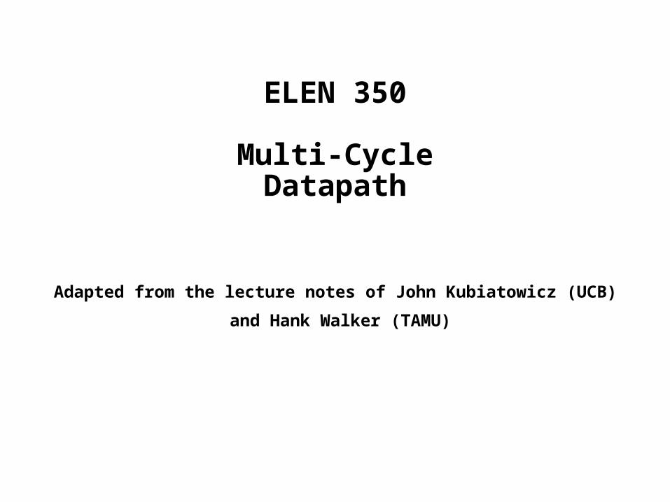
Abstract View of our single cycle processor
° looks like a FSM with PC as state
PC
Nex
t P
C
Reg
iste
rF
etch ALU Reg
. W
rt
Mem
Acc
ess
Dat
aM
emInst
ruct
ion
Fet
ch
AL
Uct
r
Reg
Dst
AL
US
rc
Ext
Op
Mem
Wr
Eq
ual
nPC
_sel
Reg
Wr
Mem
Wr
Mem
Rd
ControlUnit
op
fun
Ext

What’s wrong with our CPI=1 processor?
° All instructions take as much time as the slowest
° Long Cycle Time
° Real memory is not as nice as our idealized memory• cannot always get the job done in one (short) cycle
PC Inst Memory mux ALU Data Mem mux
PC Reg FileInst Memory mux ALU mux
PC Inst Memory mux ALU Data Mem
PC Inst Memory cmp mux
Reg File
Reg File
Reg File
Arithmetic & Logical
Load
Store
Branch
Critical Path
setup
setup
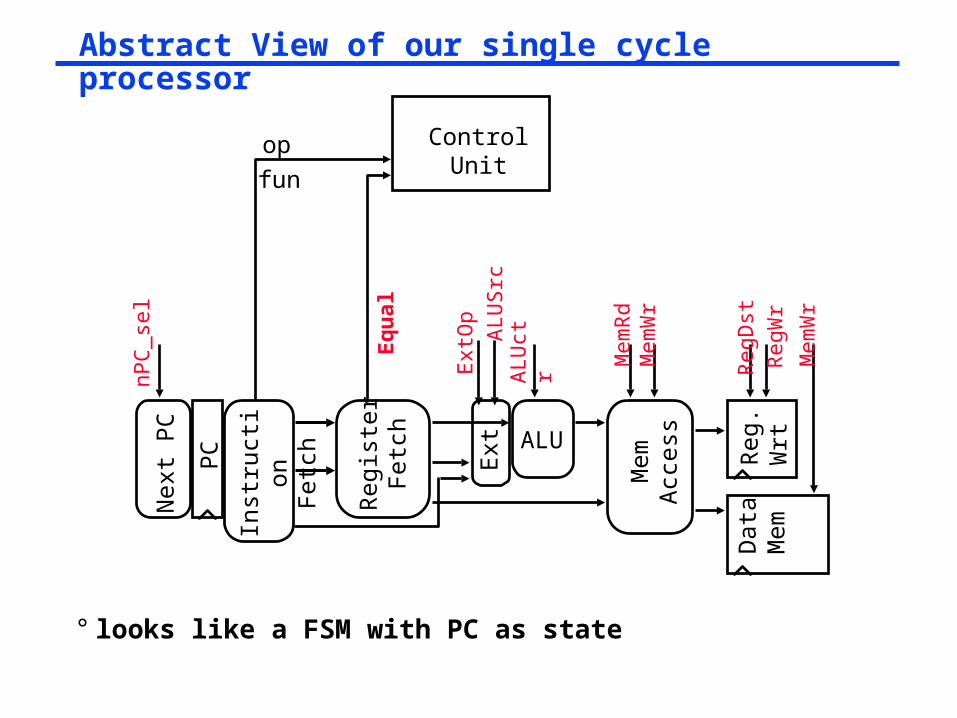
Reducing Cycle Time
° Cut combinational dependency graph and insert register / latch
° Do same work in two fast cycles, rather than one slow one
° May be able to short-circuit path and remove some components for some instructions!
storage element
CombinationalLogic
storage element
storage element
CombinationalLogic (A)
storage element
storage element
CombinationalLogic (B)
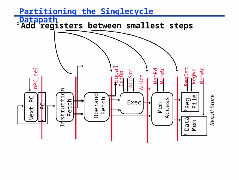
Partitioning the Singlecycle Datapath
° Add registers between smallest steps
° Place enables on all registers
PC
Nex
t P
C
Ope
rand
Fet
ch Exec Reg
. F
ile
Mem
Acc
ess
Dat
aM
em
Inst
ruct
ion
Fet
ch
Res
ult
Sto
re
AL
Uct
r
Reg
Dst
AL
US
rc
Ext
Op
Mem
Wr
nPC
_sel
Reg
Wr
Mem
Wr
Mem
Rd
Equ
al
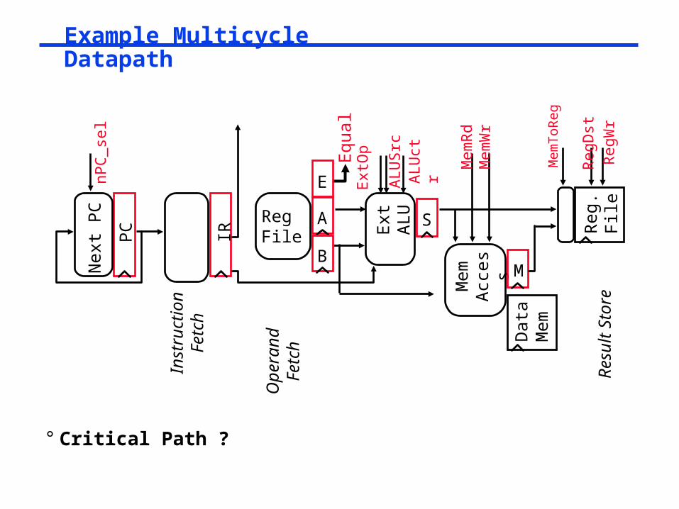
Example Multicycle Datapath
° Critical Path ?
PC
Nex
t P
C
Ope
rand
Fet
ch
Inst
ruct
ion
Fet
ch
nPC
_sel
IRRegFile E
xtA
LU Reg
. F
ile
Mem
Acc
ess
Dat
aM
em
Res
ult
Sto
reR
egD
stR
egW
r
Mem
Wr
Mem
Rd
S
M
Mem
ToR
eg
Equ
al
AL
Uct
rA
LU
Src
Ext
Op
A
B
E
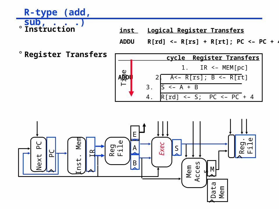
R-type (add, sub, . . .)
° Instruction
° Register Transfers
inst Logical Register Transfers
ADDU R[rd] <– R[rs] + R[rt]; PC <– PC + 4
cycle Register Transfers
1. IR <– MEM[pc]
ADDU 2. A<– R[rs]; B <– R[rt]
3. S <– A + B
4. R[rd] <– S; PC <– PC + 4
Exe
c
Reg
. F
ile
Mem
Acc
ess
Dat
aM
em
S
M
Reg
File
PC
Nex
t P
C
IR
Inst
. M
em
Tim
e
A
B
E
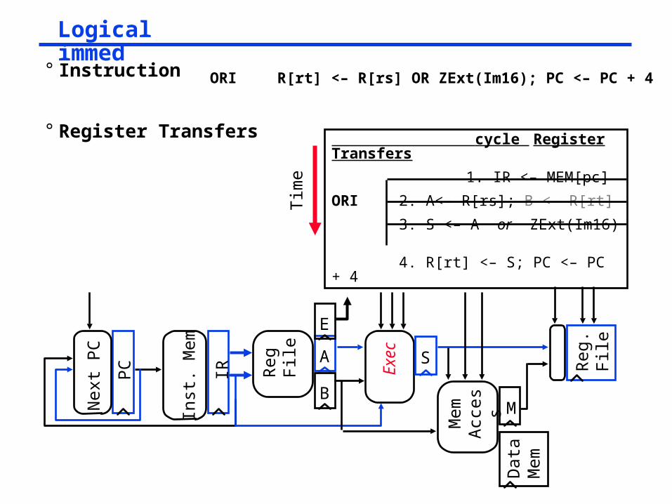
Logical immed
° Instruction
° Register Transfers
ORI R[rt] <– R[rs] OR ZExt(Im16); PC <– PC + 4
cycle Register Transfers
1. IR <– MEM[pc]
ORI 2. A<– R[rs]; B <– R[rt]
3. S <– A or ZExt(Im16)
4. R[rt] <– S; PC <– PC + 4
Exe
c
Reg
. F
ile
Mem
Acc
ess
Dat
aM
em
S
M
Reg
File
PC
Nex
t P
C
IR
Inst
. M
em
Tim
e
A
B
E
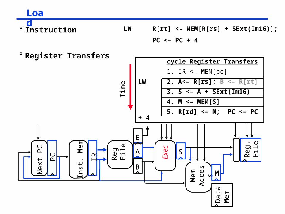
Load
° Instruction
° Register Transfers
LW R[rt] <– MEM[R[rs] + SExt(Im16)];
PC <– PC + 4
cycle Register Transfers
1. IR <– MEM[pc]
LW 2. A<– R[rs]; B <– R[rt]
3. S <– A + SExt(Im16)
4. M <– MEM[S]
5. R[rd] <– M; PC <– PC + 4
Exe
c
Reg
. F
ile
Mem
Acc
ess
Dat
aM
em
S
M
Reg
File
PC
Nex
t P
C
IR
Inst
. M
em A
B
E
Tim
e
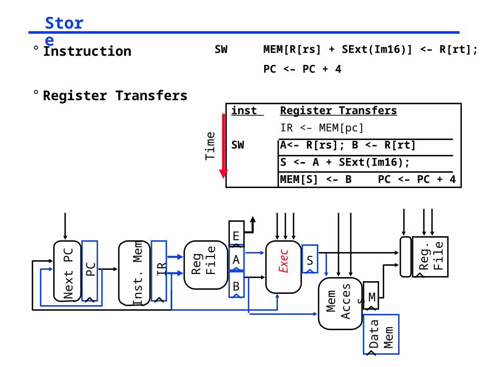
Store
° Instruction
° Register Transfers
SW MEM[R[rs] + SExt(Im16)] <– R[rt];
PC <– PC + 4
inst Register Transfers
IR <– MEM[pc]
SW A<– R[rs]; B <– R[rt]
S <– A + SExt(Im16);
MEM[S] <– B PC <– PC + 4
Exe
c
Reg
. F
ile
Mem
Acc
ess
Dat
aM
em
S
M
Reg
File
PC
Nex
t P
C
IR
Inst
. M
em A
B
E
Tim
e
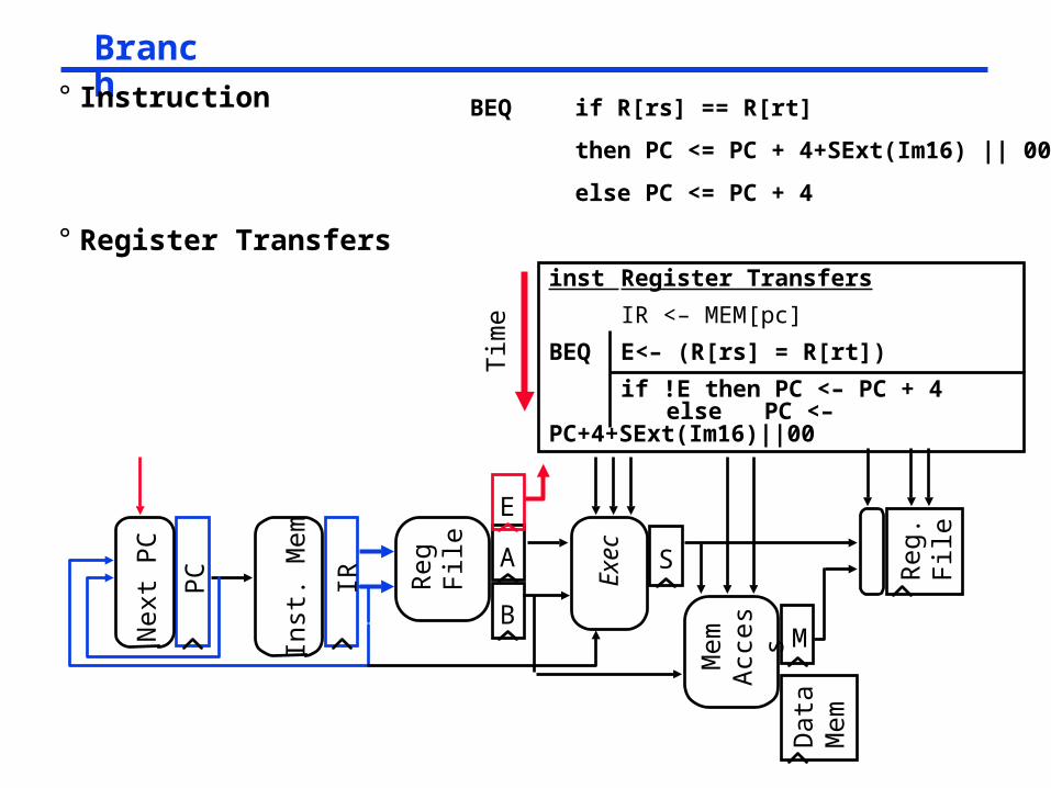
Branch° Instruction
° Register Transfers
BEQ if R[rs] == R[rt]
then PC <= PC + 4+SExt(Im16) || 00
else PC <= PC + 4
Exe
c
Reg
. F
ile
Mem
Acc
ess
Dat
aM
em
S
M
Reg
File
PC
Nex
t P
C
IR
Inst
. M
eminst Register Transfers
IR <– MEM[pc]
BEQ E<– (R[rs] = R[rt])
if !E then PC <– PC + 4 else PC <–PC+4+SExt(Im16)||00
A
B
ET
ime
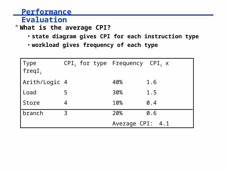
Performance Evaluation
° What is the average CPI?• state diagram gives CPI for each instruction type
• workload gives frequency of each type
Type CPIi for type Frequency CPIi x freqIi
Arith/Logic 4 40% 1.6
Load 5 30% 1.5
Store 4 10% 0.4
branch 3 20% 0.6
Average CPI:4.1
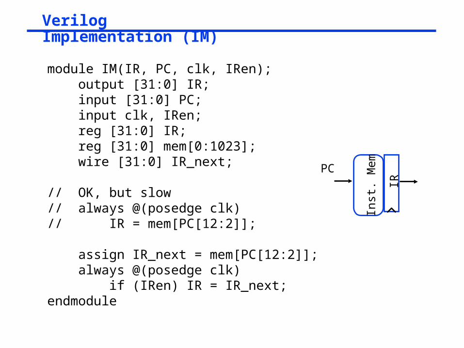
Verilog Implementation (IM)
module IM(IR, PC, clk, IRen); output [31:0] IR; input [31:0] PC; input clk, IRen; reg [31:0] IR; reg [31:0] mem[0:1023]; wire [31:0] IR_next;
// OK, but slow// always @(posedge clk)// IR = mem[PC[12:2]];
assign IR_next = mem[PC[12:2]]; always @(posedge clk) if (IRen) IR = IR_next;endmodule
IR
Inst
. M
emPC
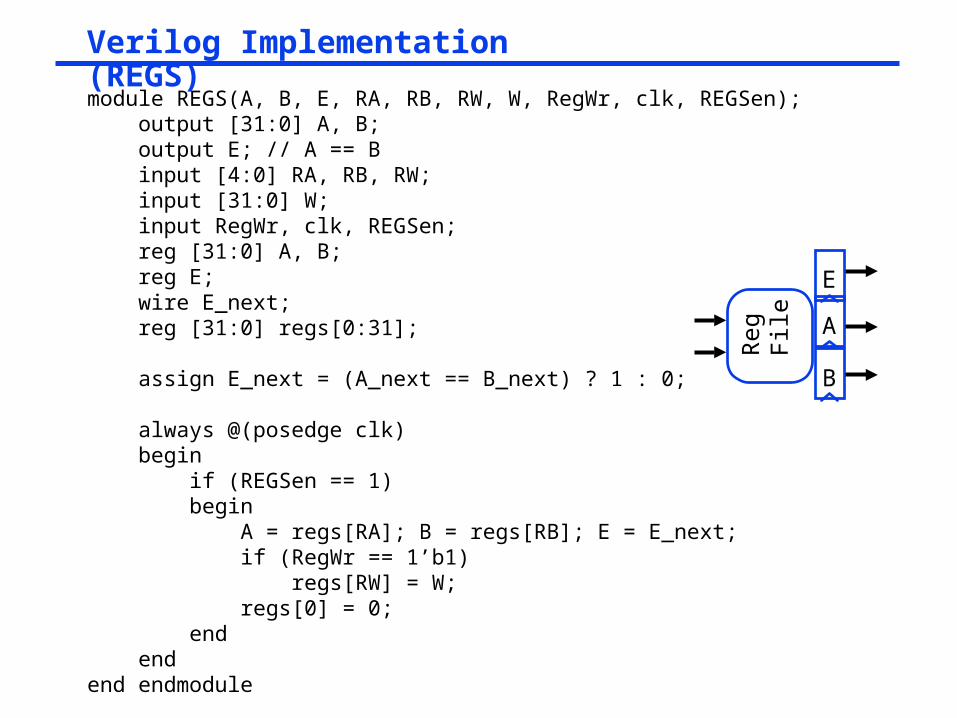
Verilog Implementation (REGS) module REGS(A, B, E, RA, RB, RW, W, RegWr, clk, REGSen); output [31:0] A, B; output E; // A == B input [4:0] RA, RB, RW; input [31:0] W; input RegWr, clk, REGSen; reg [31:0] A, B; reg E; wire E_next; reg [31:0] regs[0:31];
assign E_next = (A_next == B_next) ? 1 : 0; always @(posedge clk) begin if (REGSen == 1) begin A = regs[RA]; B = regs[RB]; E = E_next; if (RegWr == 1’b1) regs[RW] = W; regs[0] = 0; end end end endmodule
Reg
File A
B
E
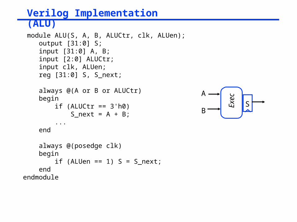
Verilog Implementation (ALU) module ALU(S, A, B, ALUCtr, clk, ALUen); output [31:0] S; input [31:0] A, B; input [2:0] ALUCtr; input clk, ALUen; reg [31:0] S, S_next;
always @(A or B or ALUCtr) begin if (ALUCtr == 3'h0) S_next = A + B; ... end
always @(posedge clk) begin if (ALUen == 1) S = S_next; endendmodule
Exe
c
S
A
B
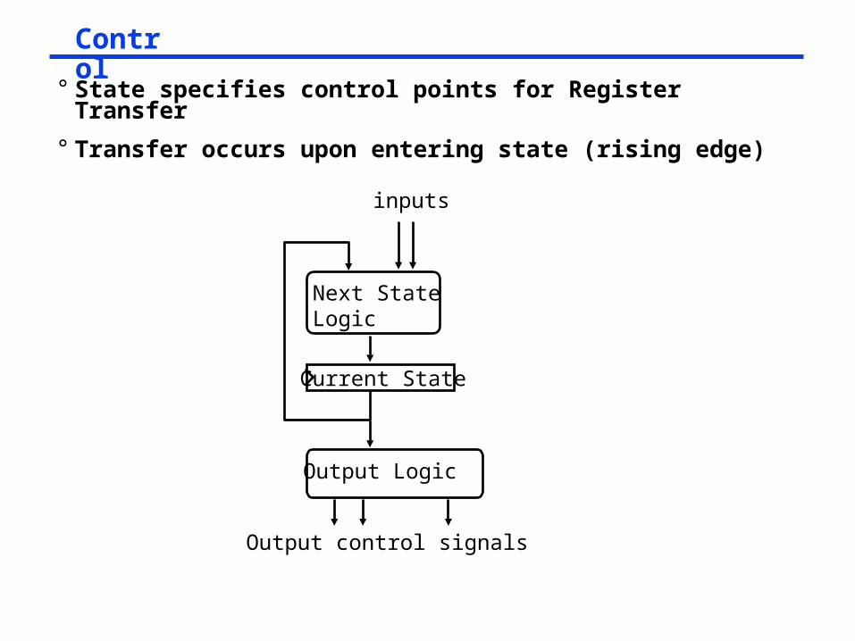
Control
° State specifies control points for Register Transfer
° Transfer occurs upon entering state (rising edge)
Current State
Next StateLogic
Output Logic
inputs
Output control signals
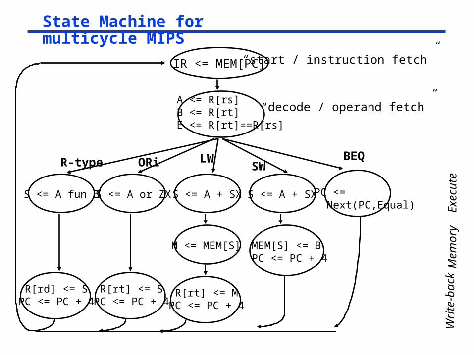
State Machine for multicycle MIPS
IR <= MEM[PC]
R-type
A <= R[rs]B <= R[rt]E <= R[rt]==R[rs]
S <= A fun B
R[rd] <= SPC <= PC + 4
S <= A or ZX
R[rt] <= SPC <= PC + 4
ORi
S <= A + SX
R[rt] <= MPC <= PC + 4
M <= MEM[S]
LW
S <= A + SX
MEM[S] <= BPC <= PC + 4
BEQ
PC <= Next(PC,Equal)
SW
“start / instruction fetch”
“decode / operand fetch”
Exe
cute
Mem
ory
Writ
e-ba
ck
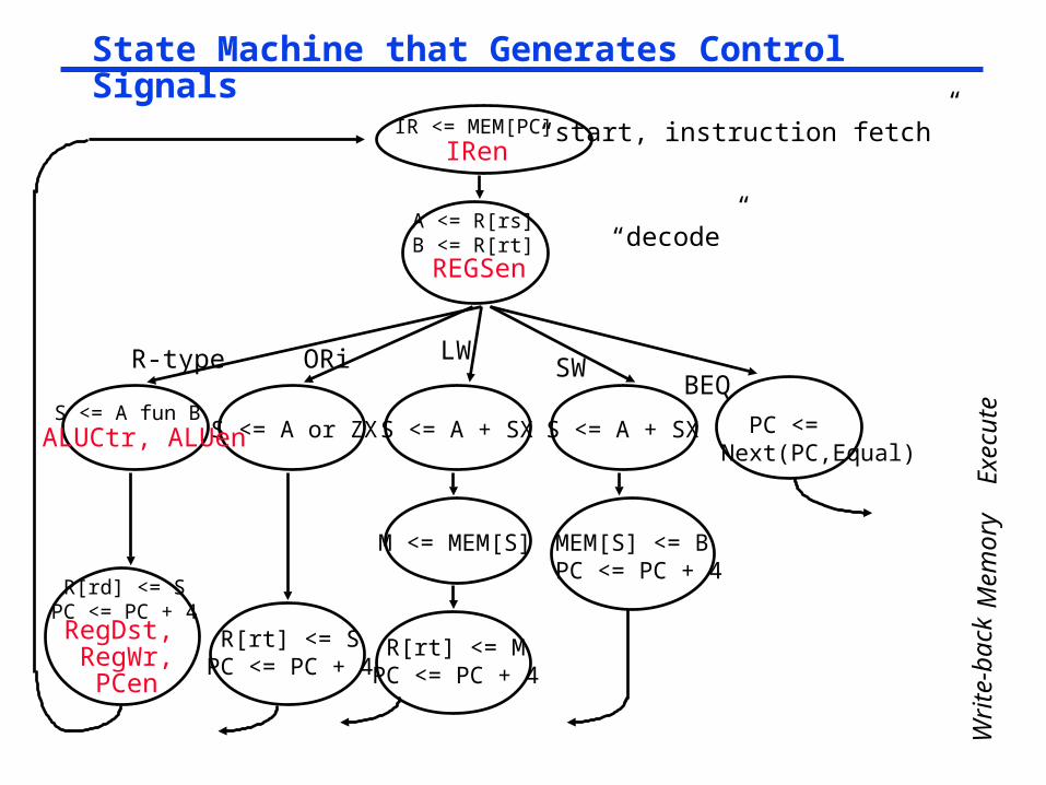
State Machine that Generates Control Signals
IR <= MEM[PC]
R-type
A <= R[rs]B <= R[rt]
S <= A fun B
R[rd] <= SPC <= PC + 4
S <= A or ZX
R[rt] <= SPC <= PC + 4
ORi
S <= A + SX
R[rt] <= MPC <= PC + 4
M <= MEM[S]
LW
S <= A + SX
MEM[S] <= BPC <= PC + 4
BEQ
PC <= Next(PC,Equal)
SW
“start, instruction fetch”
“decode”
IRen
ALUCtr, ALUen
RegDst, RegWr,PCen
REGSen
Exe
cute
Mem
ory
Writ
e-ba
ck
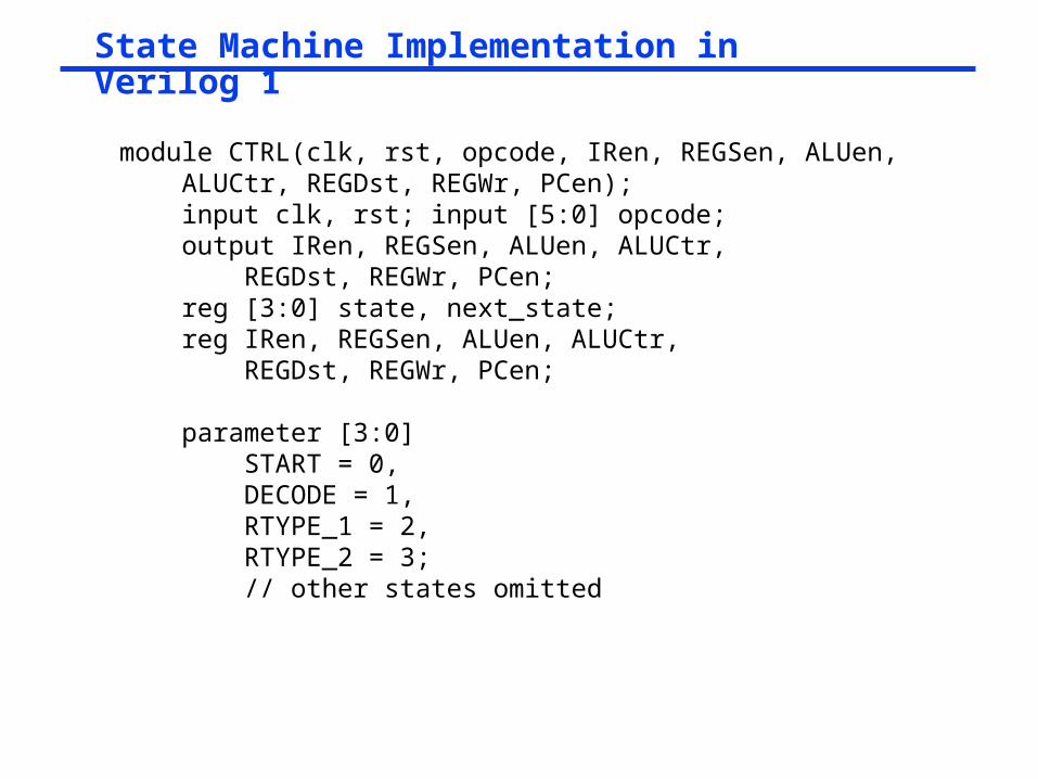
State Machine Implementation in Verilog 1
module CTRL(clk, rst, opcode, IRen, REGSen, ALUen, ALUCtr, REGDst, REGWr, PCen); input clk, rst; input [5:0] opcode; output IRen, REGSen, ALUen, ALUCtr, REGDst, REGWr, PCen; reg [3:0] state, next_state; reg IRen, REGSen, ALUen, ALUCtr, REGDst, REGWr, PCen;
parameter [3:0] START = 0, DECODE = 1, RTYPE_1 = 2, RTYPE_2 = 3; // other states omitted
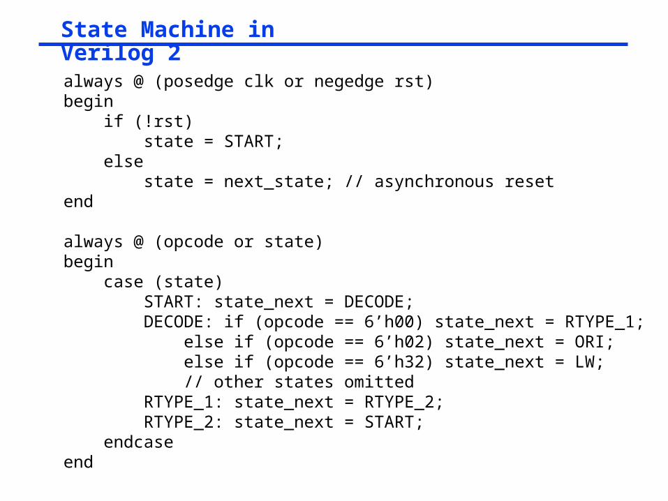
State Machine in Verilog 2always @ (posedge clk or negedge rst)begin if (!rst) state = START; else state = next_state; // asynchronous resetend
always @ (opcode or state)begin case (state) START: state_next = DECODE; DECODE: if (opcode == 6’h00) state_next = RTYPE_1; else if (opcode == 6’h02) state_next = ORI; else if (opcode == 6’h32) state_next = LW; // other states omitted RTYPE_1: state_next = RTYPE_2; RTYPE_2: state_next = START; endcaseend
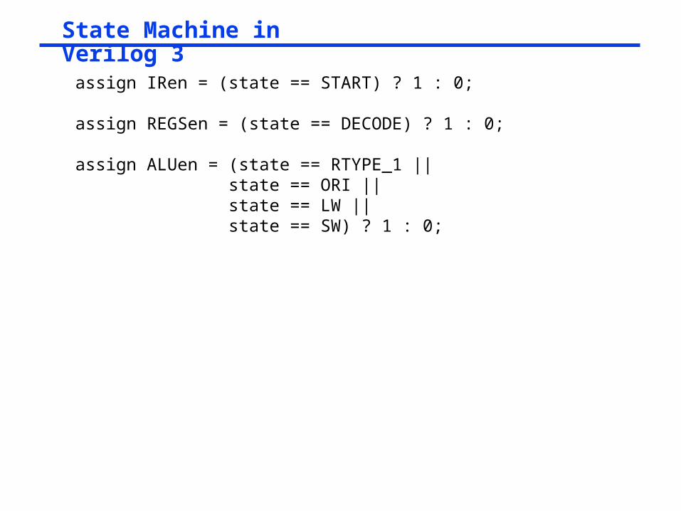
State Machine in Verilog 3 assign IRen = (state == START) ? 1 : 0;
assign REGSen = (state == DECODE) ? 1 : 0;
assign ALUen = (state == RTYPE_1 || state == ORI || state == LW || state == SW) ? 1 : 0;
Assigning States
IR <= MEM[PC]
R-type
A <= R[rs]B <= R[rt]
S <= A fun B
R[rd] <= SPC <= PC + 4
S <= A or ZX
R[rt] <= SPC <= PC + 4
ORi
S <= A + SX
R[rt] <= MPC <= PC + 4
M <= MEM[S]
LW
S <= A + SX
MEM[S] <= BPC <= PC + 4
BEQ
PC <= Next(PC)
SW
“start, instruction fetch”
“decode”
0000
0001
0100
0101
0110
0111
1000
1001
1010
00111011
1100
Exe
cute
Mem
ory
Writ
e-ba
ck
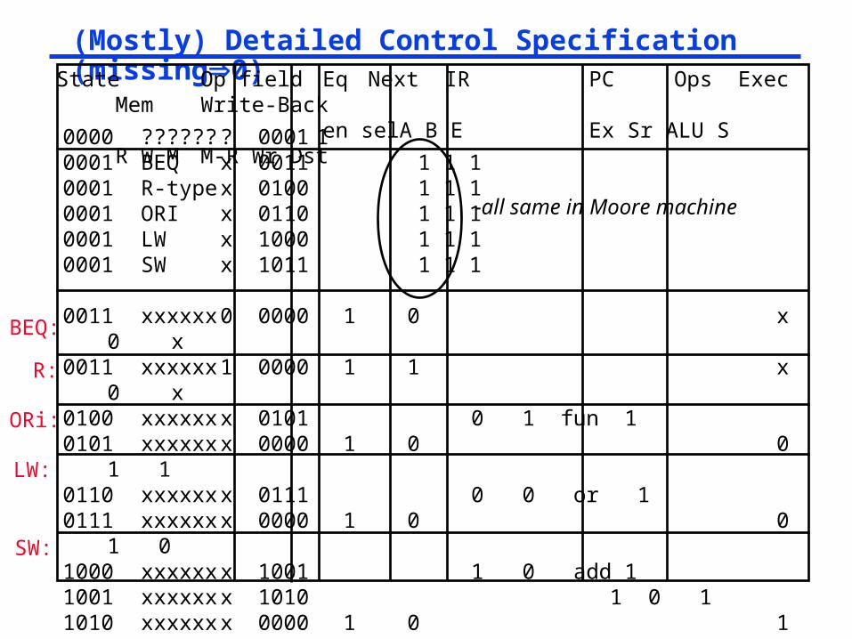
(Mostly) Detailed Control Specification (missing0)
0000 ?????? ? 0001 10001 BEQ x 0011 1 1 1 0001 R-type x 0100 1 1 1 0001 ORI x 0110 1 1 10001 LW x 1000 1 1 10001 SW x 1011 1 1 1
0011 xxxxxx 0 0000 1 0 x 0 x0011 xxxxxx 1 0000 1 1 x 0 x0100 xxxxxx x 0101 0 1 fun 10101 xxxxxx x 0000 1 0 0 1 10110 xxxxxx x 0111 0 0 or 10111 xxxxxx x 0000 1 0 0 1 01000 xxxxxx x 1001 1 0 add 11001 xxxxxx x 1010 1 0 11010 xxxxxx x 0000 1 0 1 1 01011 xxxxxx x 1100 1 0 add 11100 xxxxxx x 0000 1 0 0 1 0
State Op field Eq Next IR PC Ops Exec Mem Write-Backen sel A B E Ex Sr ALU S R W M M-R Wr Dst
R:
ORi:
LW:
SW:
-all same in Moore machine
BEQ:
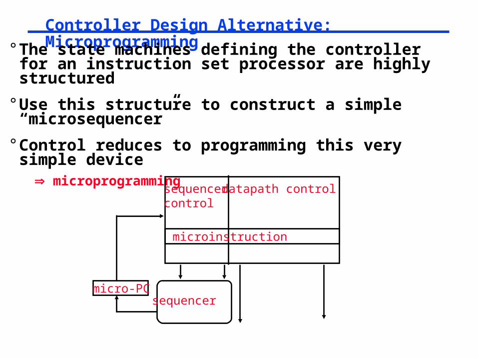
Controller Design Alternative: Microprogramming° The state machines defining the controller for an
instruction set processor are highly structured
° Use this structure to construct a simple “microsequencer”
° Control reduces to programming this very simple device microprogramming
sequencercontrol
datapath control
micro-PCsequencer
microinstruction