Embed Size (px)
Citation preview

ELTR 140 (Digital 1), section 1
Recommended schedule
Day 1Topics: Logic states and simple gate circuitsQuestions: 1 through 10Lab Exercise: OR gate, diode-resistor logic (question 51)
Day 2Topics: TTL logic gates and truth tablesQuestions: 11 through 20Lab Exercise: AND gate, simple BJT logic (question 52)
Day 3Topics: CMOS logic gates and truth tablesQuestions: 21 through 30Lab Exercise: IC logic gate usage (question 53)
Day 4Topics: Relay circuits and truth tablesQuestions: 31 through 40Lab Exercise: AND gate, relay logic (question 54)
Day 5Topics: Logic circuit performance parametersQuestions: 41 through 50Lab Exercise: Gate-relay interposing (question 55)
Day 6Exam 1: includes IC logic gate performance assessment
Troubleshooting practice problemsQuestions: 57 through 66
DC/AC review problemsQuestions: 67 through 86
Basic principles of microcontrollersQuestions: 87 through 96
General concept practice and challenge problemsQuestions: 97 through the end of the worksheet
Impending deadlinesProject due at end of ELTR140, Section 3Question 56: Sample project grading criteria
1

ELTR 140 (Digital 1), section 1
Project ideas
Logic probe: Uses a comparator and at least one logic gate to drive three LEDs: ”High”, ”Low”, and”Indeterminate”, showing three different voltage levels detected at the probe. The thresholds for high andlow logic levels shall be adjustable for use in different types of logic circuits.
Digital combination lock: Drives a solenoid or other power device only when the input code matches the”key” code (set by a series of switches on the circuit board), and drives an alarm siren if the input code doesnot match the ”key” code. The logic function may be done with Exclusive-OR gates or with a magnitudecomparator IC. Remember, the more bits in the codes, the harder it is to guess!
2

ELTR 140 (Digital 1), section 1
Skill standards addressed by this course section
EIA Raising the Standard; Electronics Technician Skills for Today and Tomorrow, June 1994
F Technical Skills – Digital CircuitsF.01 Demonstrate an understanding of the characteristics of integrated circuit (IC) logic families.F.05 Understand principles and operations of types of logic gates.F.06 Fabricate and demonstrate types of logic gates.F.07 Troubleshoot and repair types of logic gates.
B Basic and Practical Skills – Communicating on the JobB.01 Use effective written and other communication skills. Met by group discussion and completion of labwork.B.03 Employ appropriate skills for gathering and retaining information. Met by research and preparation
prior to group discussion.B.04 Interpret written, graphic, and oral instructions. Met by completion of labwork.B.06 Use language appropriate to the situation. Met by group discussion and in explaining completed labwork.B.07 Participate in meetings in a positive and constructive manner. Met by group discussion.B.08 Use job-related terminology. Met by group discussion and in explaining completed labwork.B.10 Document work projects, procedures, tests, and equipment failures. Met by project construction and/or
troubleshooting assessments.C Basic and Practical Skills – Solving Problems and Critical Thinking
C.01 Identify the problem. Met by research and preparation prior to group discussion.C.03 Identify available solutions and their impact including evaluating credibility of information, and locating
information. Met by research and preparation prior to group discussion.C.07 Organize personal workloads. Met by daily labwork, preparatory research, and project management.C.08 Participate in brainstorming sessions to generate new ideas and solve problems. Met by group discussion.
D Basic and Practical Skills – ReadingD.01 Read and apply various sources of technical information (e.g. manufacturer literature, codes, and
regulations). Met by research and preparation prior to group discussion.E Basic and Practical Skills – Proficiency in Mathematics
E.01 Determine if a solution is reasonable.E.02 Demonstrate ability to use a simple electronic calculator.E.06 Translate written and/or verbal statements into mathematical expressions.E.07 Compare, compute, and solve problems involving binary, octal, decimal, and hexadecimal numbering
systems.E.12 Interpret and use tables, charts, maps, and/or graphs.E.13 Identify patterns, note trends, and/or draw conclusions from tables, charts, maps, and/or graphs.E.15 Simplify and solve algebraic expressions and formulas.E.16 Select and use formulas appropriately.E.18 Use properties of exponents and logarithms.
F Additional Skills – ElectromechanicsB.01b Relays and relay circuits.
3
ELTR 140 (Digital 1), section 1
Common areas of confusion for students
Difficult concept: Necessary conditions for transistor operation.It is vitally important for students to understand the conditions necessary for transistor operation, both
for understanding how circuits work and for troubleshooting faulty circuits. Bipolar junction transistorsrequire a base current (in the proper direction) to conduct, and the collector-to-emitter voltage must beof the correct polarity to push a collector current in the proper direction as well. Both currents join atthe emitter terminal, making the emitter current the sum of the base and collector currents. Field-effecttransistors are not so picky about the direction of the controlled current, and they only require the correctgate voltage (no gate current) to establish conduction. What makes this so confusing is that there are twotypes of bipolar transistors (NPN and PNP), two types of junction field-effect transistors (N-channel and P-channel), and four types of MOSFETs (E-type N-channel, E-type P-channel, D-type N-channel, and D-typeP-channel).
Difficult concept: Current sourcing versus current sinking.It is very common in electronics work to refer to current-controlling devices as either sourcing current
to a load or sinking current from a load. This is an overt reference to conventional-flow notation, referringto whether the conventional flow moves out of the transistor from the positive power supply terminal to theload (sourcing), or whether the conventional flow moves in to the transistor from the load and then ”down”to ground (sinking). Some students grasp this concept readily, while others seem to struggle mightily withit. It is something rather essential to understand, because this terminology is extensively used by electronicsprofessionals and found in electronics literature. The key detail distinguishing the two conditions is whichpower supply rail (either +V or Gnd) is directly connected to the current-controlling device.
Difficult concept: Pullup and pulldown resistor placement.In digital circuits, resistors are often used to provide a secure logic state when an input device (such as
a switch) goes to a high-impedance (open) mode. Students often have difficulty figuring out exactly wherethese resistors should go in a circuit. The most common mistake I’ve seen is to place one of these ”pullup”or ”pulldown” resistors in series with a gate input, which will accomplish absolutely nothing. The ”trick”to getting this placement right, if you can call it a trick at all, is to literally follow the word ”pullup” or”pulldown.” A pullup resistor pulls the logic state of a wire up to the positive supply rail, and so mustconnect between the gate input and +V. A pulldown resistor pulls the logic state of a wire down to groundpotential, and so must connect between the gate input and ground. In either case, the resistor provides asure path to the opposite power rail that the input device connects to when active (closed).
4
Questions
Question 1
A rheostat (variable resistor) and a switch are both examples of electric components exhibiting differentdegrees of conductivity:
Rheostat Switch
Which of these devices would be considered discrete and which would be considered continuous in termsof their electrical conductivity? What do each of these words mean, and how might they apply to variablesin electric circuits other than conductivity?
file 02753
Question 2
Digital logic circuitry makes use of discrete voltage levels: each ”logic gate” sub-circuit inputs andoutputs voltages that are either considered ”high” or ”low”. Define what both of these terms means in adigital logic circuit powered by 5 volts DC.
file 02755
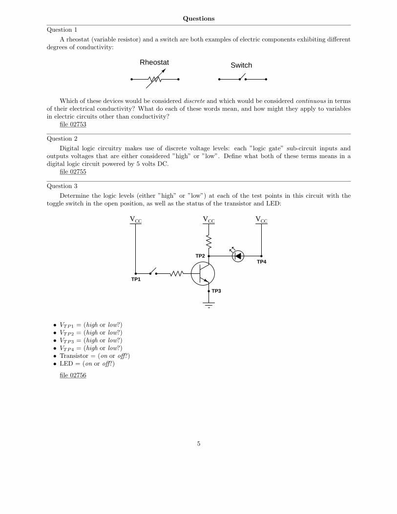
Question 3
Determine the logic levels (either ”high” or ”low”) at each of the test points in this circuit with thetoggle switch in the open position, as well as the status of the transistor and LED:
VCCVCC VCC
TP1
TP2
TP3
TP4
• VTP1 = (high or low?)• VTP2 = (high or low?)• VTP3 = (high or low?)• VTP4 = (high or low?)• Transistor = (on or off?)• LED = (on or off?)
file 02756
5
Question 4
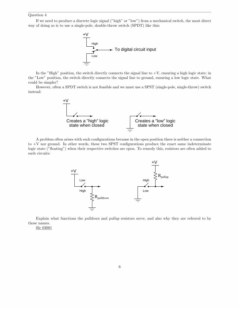
If we need to produce a discrete logic signal (”high” or ”low”) from a mechanical switch, the most directway of doing so is to use a single-pole, double-throw switch (SPDT) like this:
+V
To digital circuit inputHigh
Low
In the ”High” position, the switch directly connects the signal line to +V, ensuring a high logic state; inthe ”Low” position, the switch directly connects the signal line to ground, ensuring a low logic state. Whatcould be simpler?
However, often a SPDT switch is not feasible and we must use a SPST (single-pole, single-throw) switchinstead:
+V
Creates a "high" logicstate when closed
Creates a "low" logicstate when closed
A problem often arises with such configurations because in the open position there is neither a connectionto +V nor ground. In other words, these two SPST configurations produce the exact same indeterminatelogic state (”floating”) when their respective switches are open. To remedy this, resistors are often added tosuch circuits:
+V
High Low
Rpulldown
+V
RpullupLow High
Explain what functions the pulldown and pullup resistors serve, and also why they are referred to bythose names.
file 03001
6
Question 5
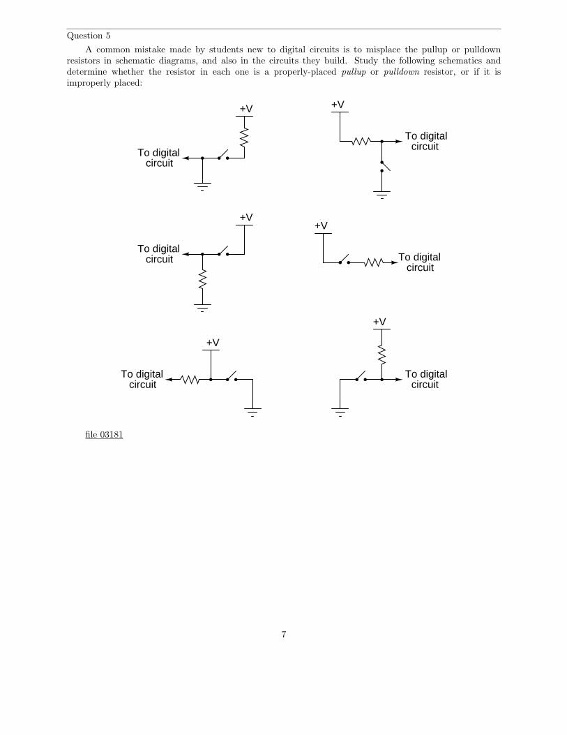
A common mistake made by students new to digital circuits is to misplace the pullup or pulldownresistors in schematic diagrams, and also in the circuits they build. Study the following schematics anddetermine whether the resistor in each one is a properly-placed pullup or pulldown resistor, or if it isimproperly placed:
+V
+V
To digitalcircuit
circuitTo digital
+V
circuitTo digital
+V
circuitTo digital
+V
To digitalcircuit
+V
circuitTo digital
file 03181
7
Question 6
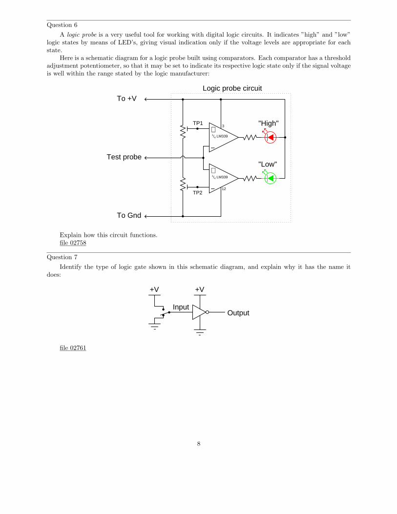
A logic probe is a very useful tool for working with digital logic circuits. It indicates ”high” and ”low”logic states by means of LED’s, giving visual indication only if the voltage levels are appropriate for eachstate.
Here is a schematic diagram for a logic probe built using comparators. Each comparator has a thresholdadjustment potentiometer, so that it may be set to indicate its respective logic state only if the signal voltageis well within the range stated by the logic manufacturer:
−
+
−
+
"High"
"Low"Test probe
1/4 LM339
1/4 LM339
3
12
TP1
TP2
Logic probe circuitTo +V
To Gnd
Explain how this circuit functions.file 02758
Question 7
Identify the type of logic gate shown in this schematic diagram, and explain why it has the name itdoes:
+V+V
OutputInput
file 02761
8
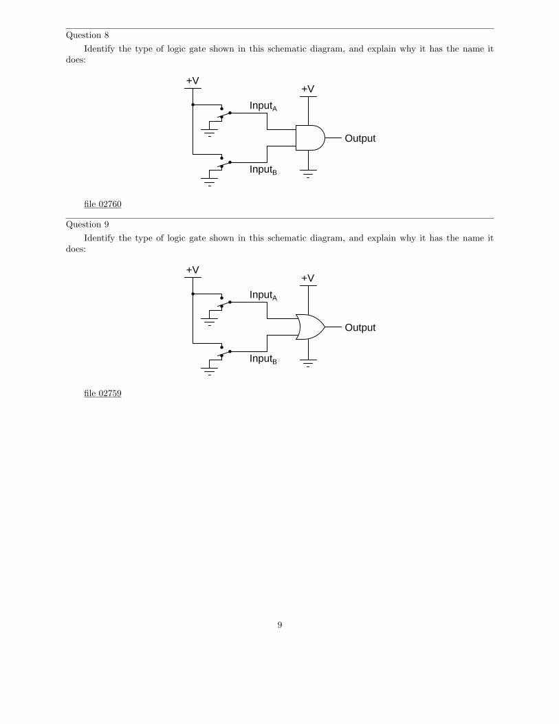
Question 8
Identify the type of logic gate shown in this schematic diagram, and explain why it has the name itdoes:
+V+V
Output
InputA
InputB
file 02760
Question 9
Identify the type of logic gate shown in this schematic diagram, and explain why it has the name itdoes:
+V+V
Output
InputA
InputB
file 02759
9
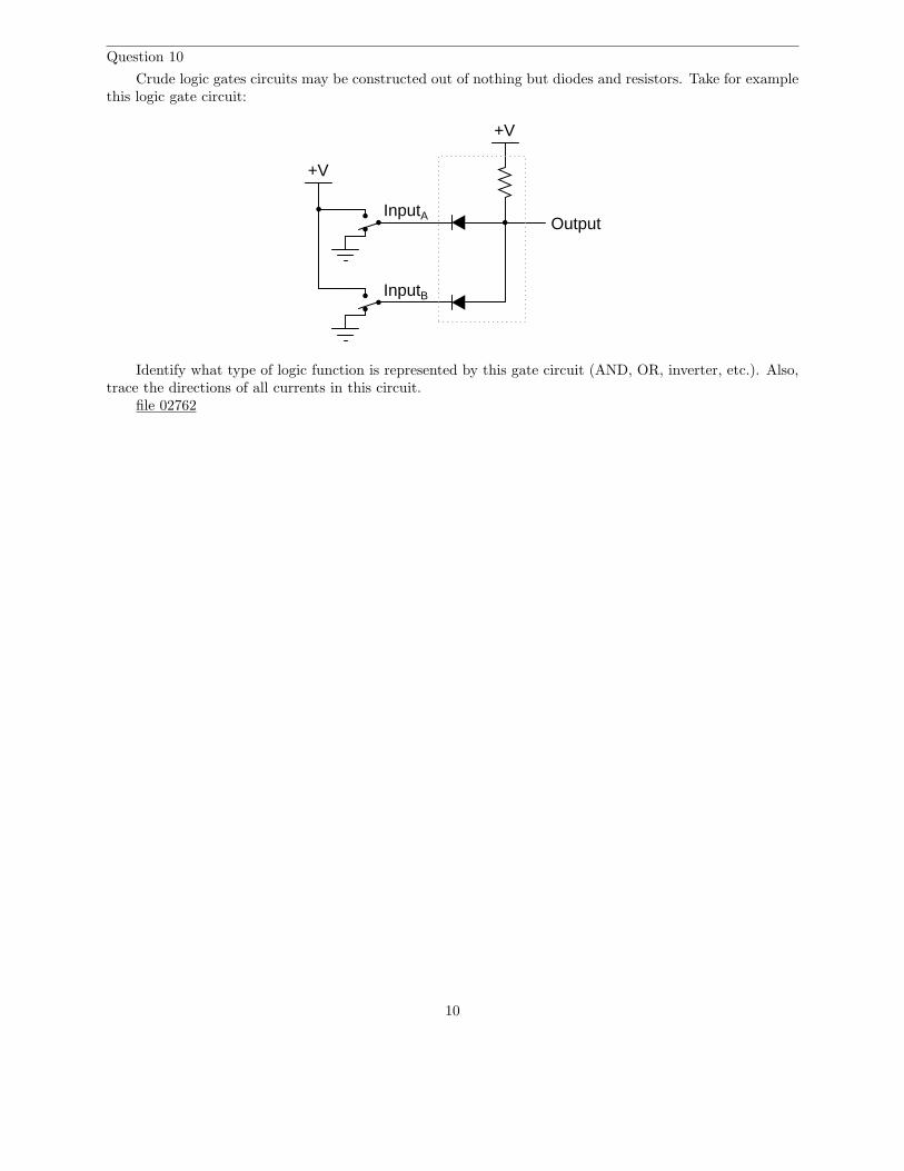
Question 10
Crude logic gates circuits may be constructed out of nothing but diodes and resistors. Take for examplethis logic gate circuit:
+V
+V
OutputInputA
InputB
Identify what type of logic function is represented by this gate circuit (AND, OR, inverter, etc.). Also,trace the directions of all currents in this circuit.
file 02762
10
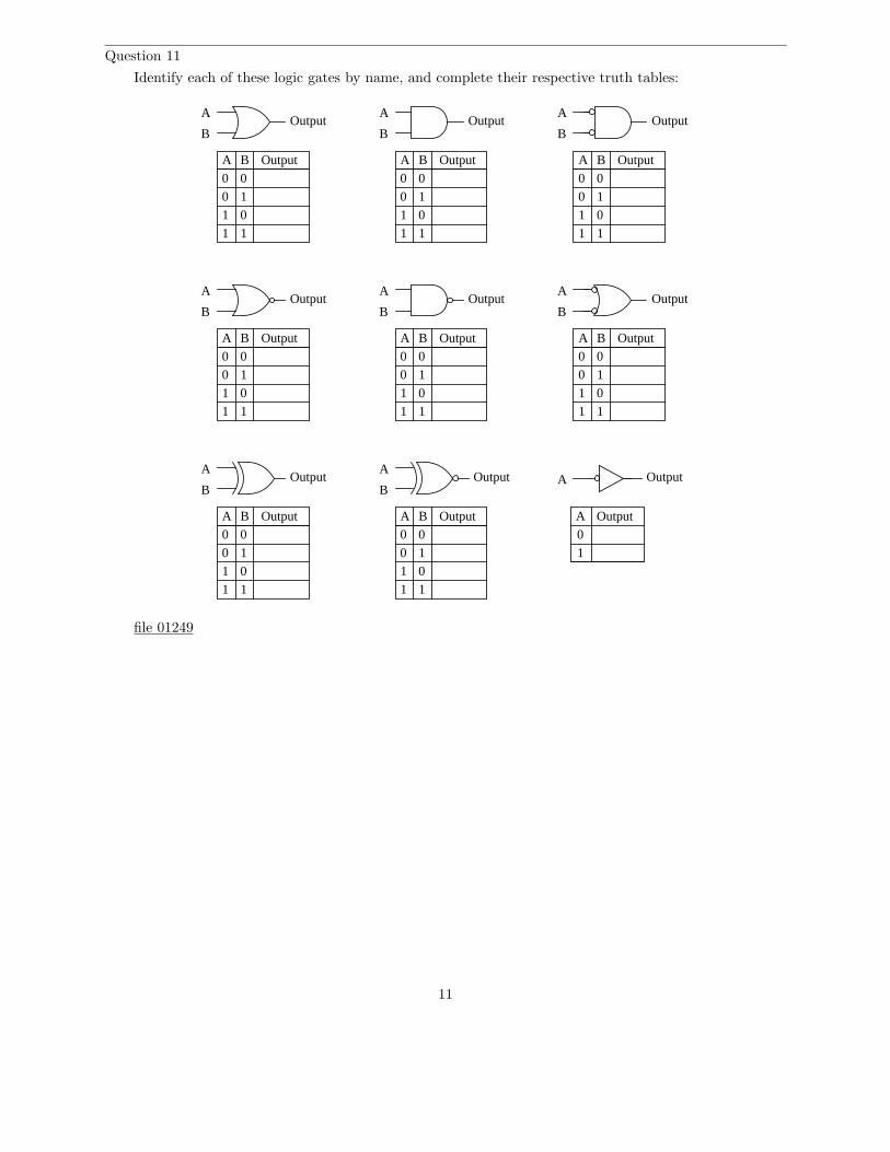
Question 11
Identify each of these logic gates by name, and complete their respective truth tables:
A B Output
00
0 1
01
1 1
A
BOutput
A B Output
00
0 1
01
1 1
A
BOutput
A B Output
00
0 1
01
1 1
A
BOutput
A B Output
00
0 1
01
1 1
A
BOutput
A B Output
00
0 1
01
1 1
A
BOutput
A B Output
00
0 1
01
1 1
A
BOutput
A B Output
00
0 1
01
1 1
A
BOutput
A B Output
00
0 1
01
1 1
A
BOutput A Output
A Output
0
1
file 01249
11
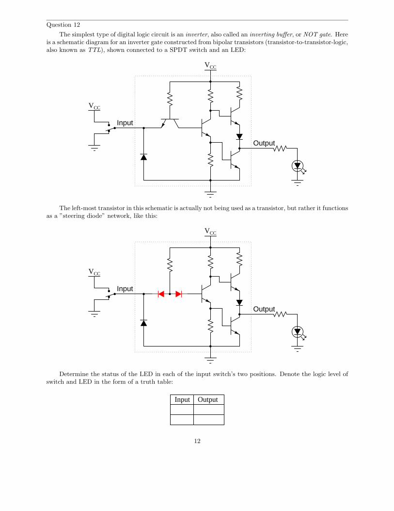
Question 12
The simplest type of digital logic circuit is an inverter, also called an inverting buffer, or NOT gate. Hereis a schematic diagram for an inverter gate constructed from bipolar transistors (transistor-to-transistor-logic,also known as TTL), shown connected to a SPDT switch and an LED:
VCC
Input
Output
VCC
The left-most transistor in this schematic is actually not being used as a transistor, but rather it functionsas a ”steering diode” network, like this:
VCC
Input
Output
VCC
Determine the status of the LED in each of the input switch’s two positions. Denote the logic level ofswitch and LED in the form of a truth table:
Input Output
12
file 01256
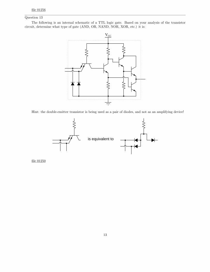
Question 13
The following is an internal schematic of a TTL logic gate. Based on your analysis of the transistorcircuit, determine what type of gate (AND, OR, NAND, NOR, XOR, etc.) it is:
VCC
Hint: the double-emitter transistor is being used as a pair of diodes, and not as an amplifying device!
is equivalent to
file 01250
13
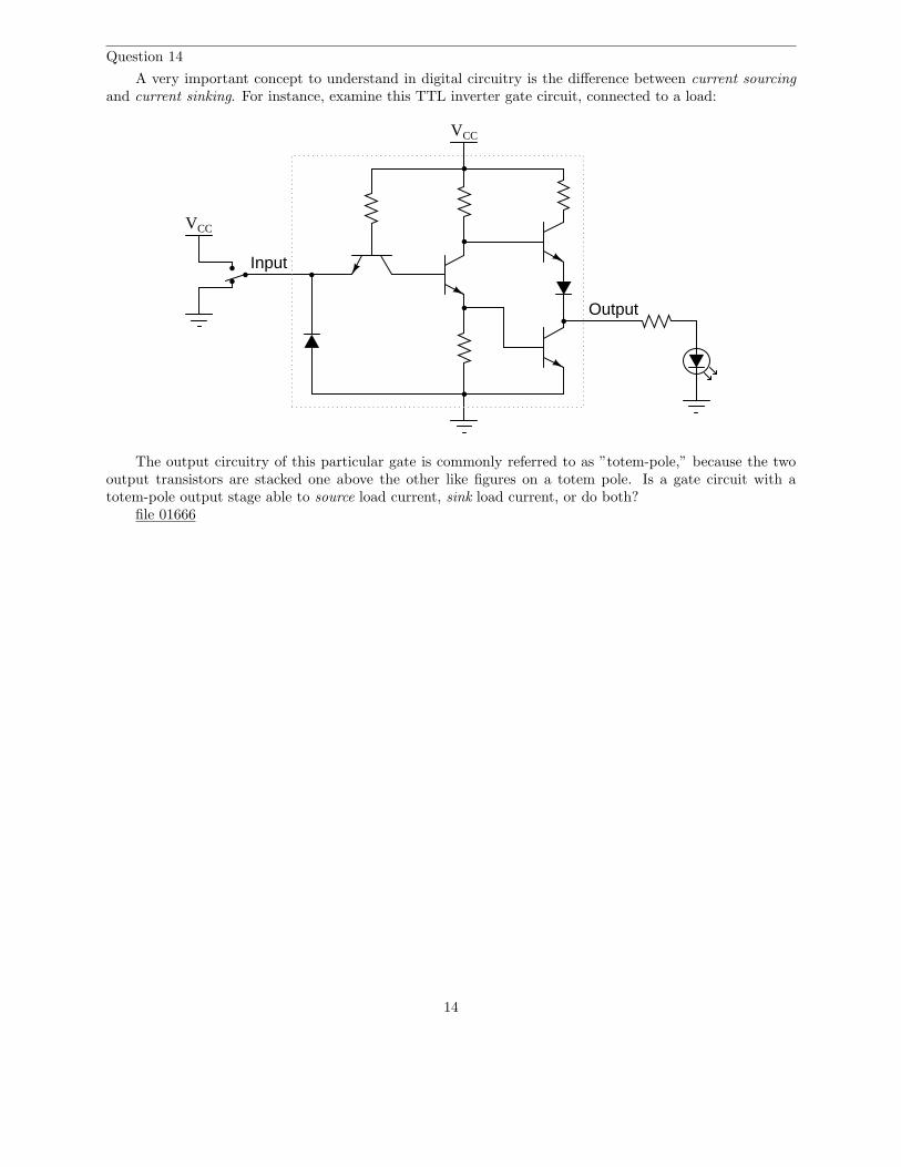
Question 14
A very important concept to understand in digital circuitry is the difference between current sourcingand current sinking. For instance, examine this TTL inverter gate circuit, connected to a load:
VCC
Input
Output
VCC
The output circuitry of this particular gate is commonly referred to as ”totem-pole,” because the twooutput transistors are stacked one above the other like figures on a totem pole. Is a gate circuit with atotem-pole output stage able to source load current, sink load current, or do both?
file 01666
14
Question 15
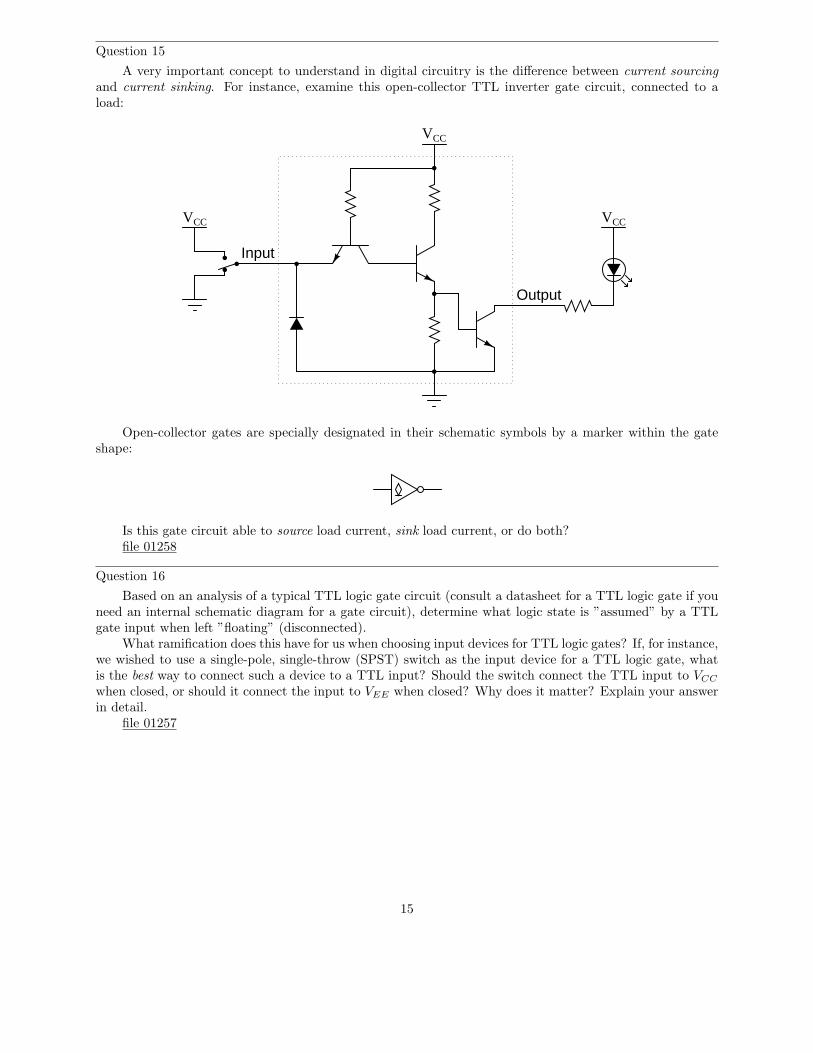
A very important concept to understand in digital circuitry is the difference between current sourcingand current sinking. For instance, examine this open-collector TTL inverter gate circuit, connected to aload:
VCC
Input
Output
VCC VCC
Open-collector gates are specially designated in their schematic symbols by a marker within the gateshape:
Is this gate circuit able to source load current, sink load current, or do both?file 01258
Question 16
Based on an analysis of a typical TTL logic gate circuit (consult a datasheet for a TTL logic gate if youneed an internal schematic diagram for a gate circuit), determine what logic state is ”assumed” by a TTLgate input when left ”floating” (disconnected).
What ramification does this have for us when choosing input devices for TTL logic gates? If, for instance,we wished to use a single-pole, single-throw (SPST) switch as the input device for a TTL logic gate, whatis the best way to connect such a device to a TTL input? Should the switch connect the TTL input to VCC
when closed, or should it connect the input to VEE when closed? Why does it matter? Explain your answerin detail.
file 01257
15
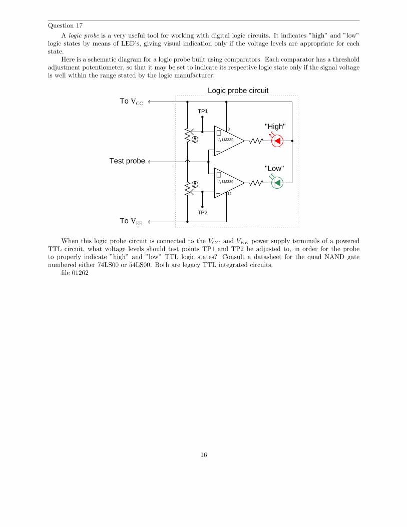
Question 17
A logic probe is a very useful tool for working with digital logic circuits. It indicates ”high” and ”low”logic states by means of LED’s, giving visual indication only if the voltage levels are appropriate for eachstate.
Here is a schematic diagram for a logic probe built using comparators. Each comparator has a thresholdadjustment potentiometer, so that it may be set to indicate its respective logic state only if the signal voltageis well within the range stated by the logic manufacturer:
−
+
−
+
"High"
"Low"Test probe
To VCC
To VEE
1/4 LM339
1/4 LM339
3
12
TP1
TP2
Logic probe circuit
When this logic probe circuit is connected to the VCC and VEE power supply terminals of a poweredTTL circuit, what voltage levels should test points TP1 and TP2 be adjusted to, in order for the probeto properly indicate ”high” and ”low” TTL logic states? Consult a datasheet for the quad NAND gatenumbered either 74LS00 or 54LS00. Both are legacy TTL integrated circuits.
file 01262
16
Question 18
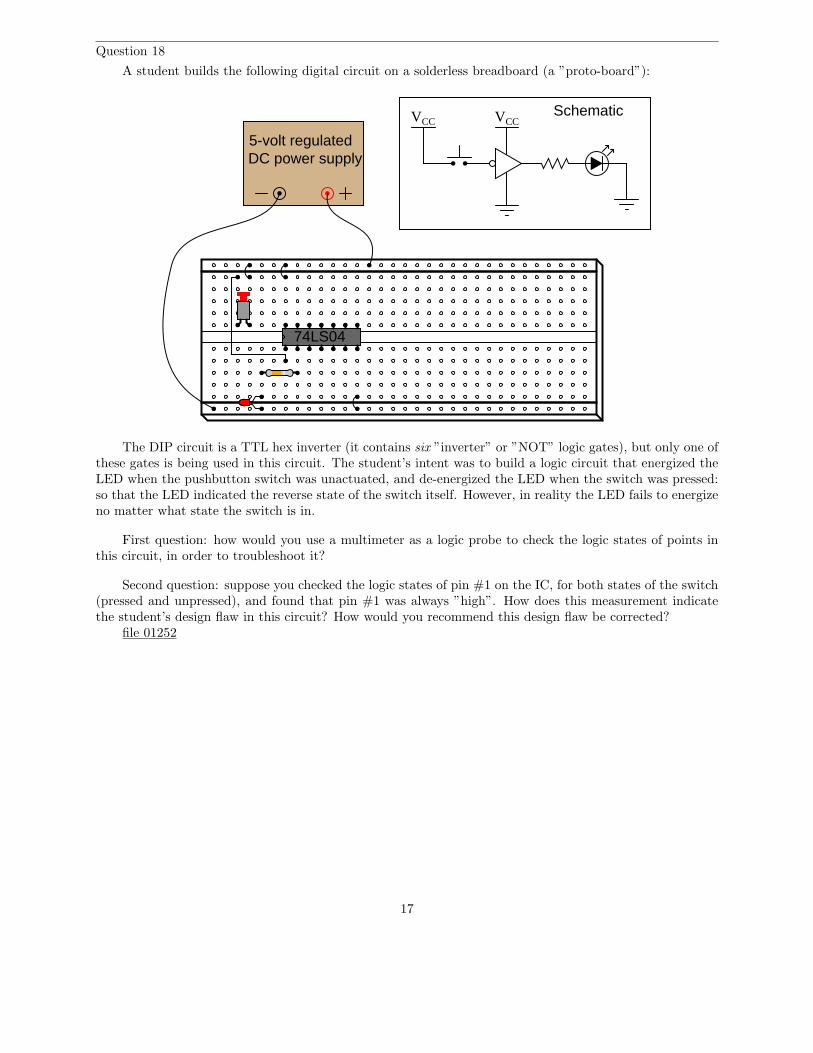
A student builds the following digital circuit on a solderless breadboard (a ”proto-board”):
5-volt regulatedDC power supply
74LS04
VCCVCCSchematic
The DIP circuit is a TTL hex inverter (it contains six ”inverter” or ”NOT” logic gates), but only one ofthese gates is being used in this circuit. The student’s intent was to build a logic circuit that energized theLED when the pushbutton switch was unactuated, and de-energized the LED when the switch was pressed:so that the LED indicated the reverse state of the switch itself. However, in reality the LED fails to energizeno matter what state the switch is in.
First question: how would you use a multimeter as a logic probe to check the logic states of points inthis circuit, in order to troubleshoot it?
Second question: suppose you checked the logic states of pin #1 on the IC, for both states of the switch(pressed and unpressed), and found that pin #1 was always ”high”. How does this measurement indicatethe student’s design flaw in this circuit? How would you recommend this design flaw be corrected?
file 01252
17
Question 19
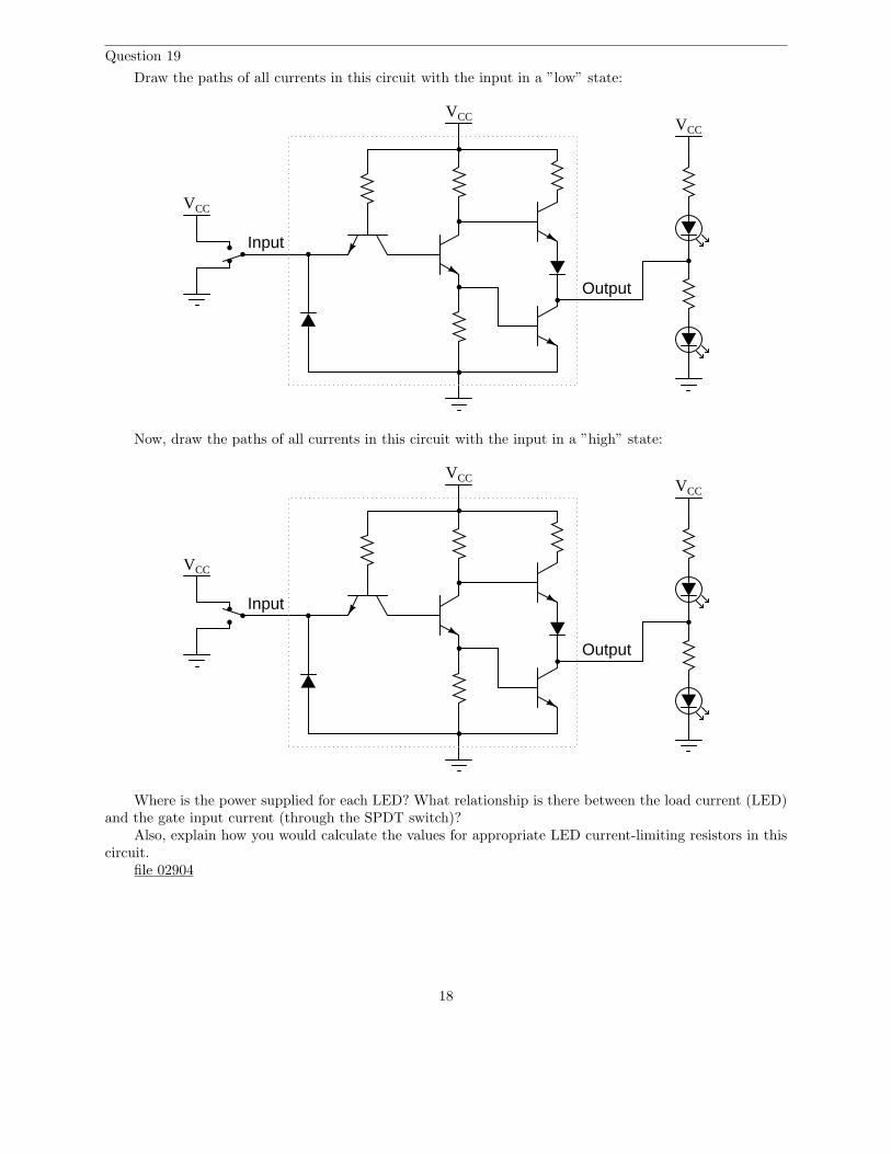
Draw the paths of all currents in this circuit with the input in a ”low” state:
VCC
Input
Output
VCC
VCC
Now, draw the paths of all currents in this circuit with the input in a ”high” state:
VCC
Input
Output
VCC
VCC
Where is the power supplied for each LED? What relationship is there between the load current (LED)and the gate input current (through the SPDT switch)?
Also, explain how you would calculate the values for appropriate LED current-limiting resistors in thiscircuit.
file 02904
18
Question 20
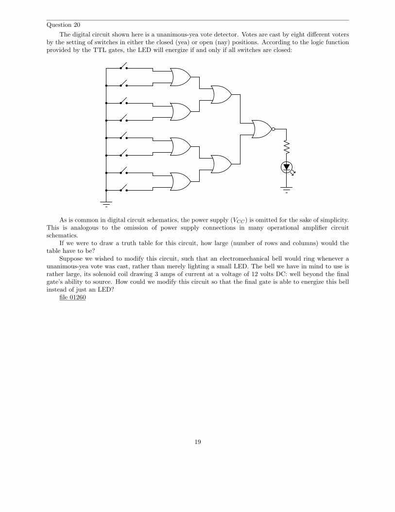
The digital circuit shown here is a unanimous-yea vote detector. Votes are cast by eight different votersby the setting of switches in either the closed (yea) or open (nay) positions. According to the logic functionprovided by the TTL gates, the LED will energize if and only if all switches are closed:
As is common in digital circuit schematics, the power supply (VCC) is omitted for the sake of simplicity.This is analogous to the omission of power supply connections in many operational amplifier circuitschematics.
If we were to draw a truth table for this circuit, how large (number of rows and columns) would thetable have to be?
Suppose we wished to modify this circuit, such that an electromechanical bell would ring whenever aunanimous-yea vote was cast, rather than merely lighting a small LED. The bell we have in mind to use israther large, its solenoid coil drawing 3 amps of current at a voltage of 12 volts DC: well beyond the finalgate’s ability to source. How could we modify this circuit so that the final gate is able to energize this bellinstead of just an LED?
file 01260
19
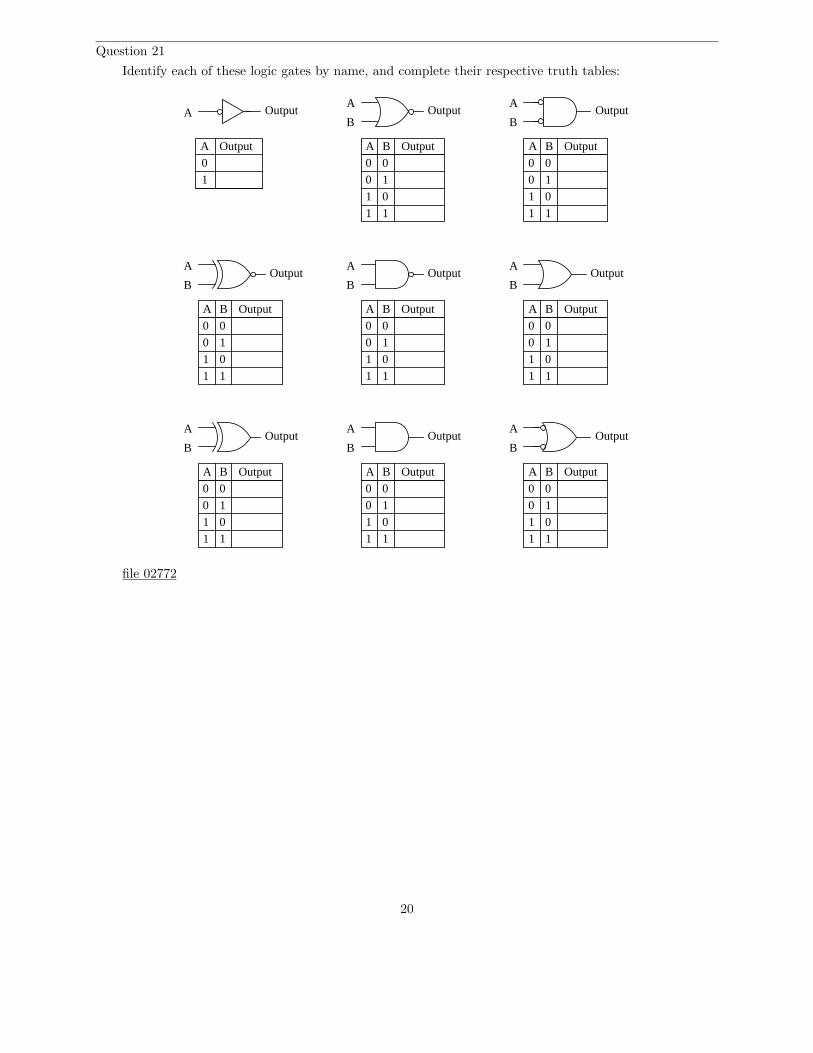
Question 21
Identify each of these logic gates by name, and complete their respective truth tables:
A B Output
00
0 1
01
1 1
A
BOutput
A B Output
00
0 1
01
1 1
A
BOutput
A B Output
00
0 1
01
1 1
A
BOutput
A B Output
00
0 1
01
1 1
A
BOutput
A B Output
00
0 1
01
1 1
A
BOutput
A B Output
00
0 1
01
1 1
A
BOutput
A B Output
00
0 1
01
1 1
A
BOutput
A B Output
00
0 1
01
1 1
A
BOutput
A Output
A Output
0
1
file 02772
20
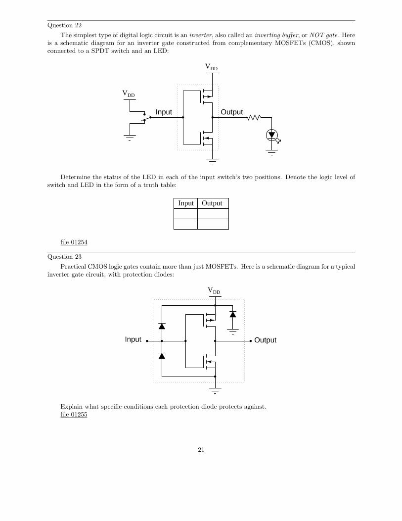
Question 22
The simplest type of digital logic circuit is an inverter, also called an inverting buffer, or NOT gate. Hereis a schematic diagram for an inverter gate constructed from complementary MOSFETs (CMOS), shownconnected to a SPDT switch and an LED:
VDD
Input
VDD
Output
Determine the status of the LED in each of the input switch’s two positions. Denote the logic level ofswitch and LED in the form of a truth table:
Input Output
file 01254
Question 23
Practical CMOS logic gates contain more than just MOSFETs. Here is a schematic diagram for a typicalinverter gate circuit, with protection diodes:
VDD
Input Output
Explain what specific conditions each protection diode protects against.file 01255
21
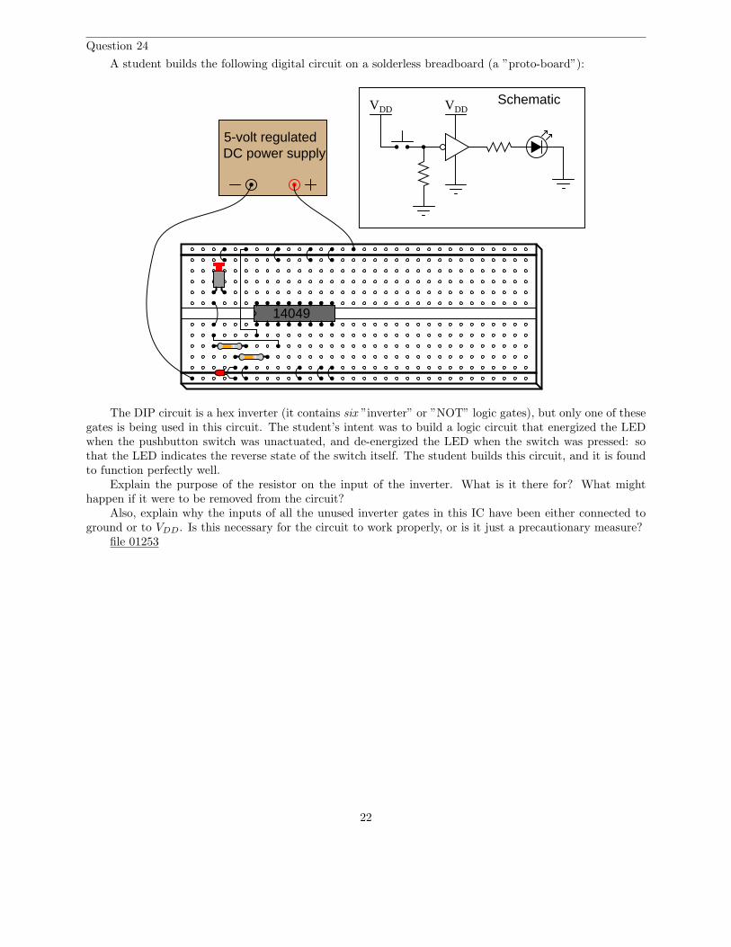
Question 24
A student builds the following digital circuit on a solderless breadboard (a ”proto-board”):
5-volt regulatedDC power supply
Schematic
14049
VDD VDD
The DIP circuit is a hex inverter (it contains six ”inverter” or ”NOT” logic gates), but only one of thesegates is being used in this circuit. The student’s intent was to build a logic circuit that energized the LEDwhen the pushbutton switch was unactuated, and de-energized the LED when the switch was pressed: sothat the LED indicates the reverse state of the switch itself. The student builds this circuit, and it is foundto function perfectly well.
Explain the purpose of the resistor on the input of the inverter. What is it there for? What mighthappen if it were to be removed from the circuit?
Also, explain why the inputs of all the unused inverter gates in this IC have been either connected toground or to VDD. Is this necessary for the circuit to work properly, or is it just a precautionary measure?
file 01253
22
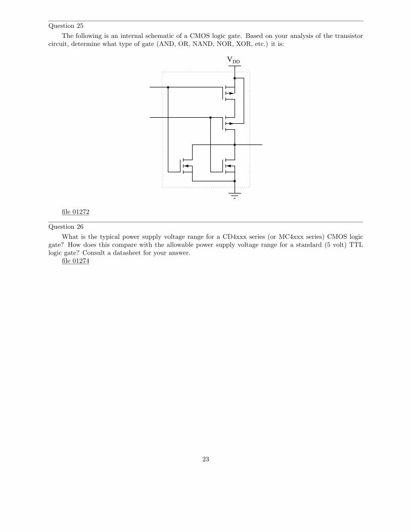
Question 25
The following is an internal schematic of a CMOS logic gate. Based on your analysis of the transistorcircuit, determine what type of gate (AND, OR, NAND, NOR, XOR, etc.) it is:
VDD
file 01272
Question 26
What is the typical power supply voltage range for a CD4xxx series (or MC4xxx series) CMOS logicgate? How does this compare with the allowable power supply voltage range for a standard (5 volt) TTLlogic gate? Consult a datasheet for your answer.
file 01274
23
Question 27
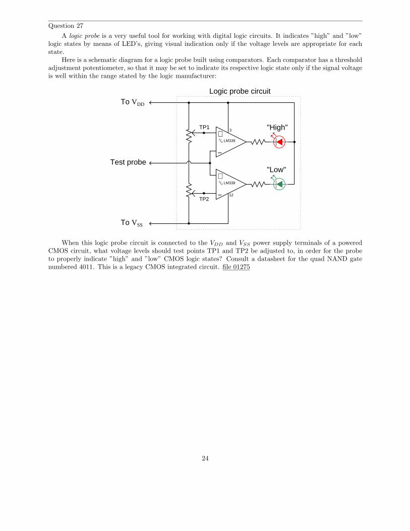
A logic probe is a very useful tool for working with digital logic circuits. It indicates ”high” and ”low”logic states by means of LED’s, giving visual indication only if the voltage levels are appropriate for eachstate.
Here is a schematic diagram for a logic probe built using comparators. Each comparator has a thresholdadjustment potentiometer, so that it may be set to indicate its respective logic state only if the signal voltageis well within the range stated by the logic manufacturer:
−
+
−
+
"High"
"Low"Test probe
1/4 LM339
1/4 LM339
3
12
TP1
TP2
Logic probe circuitTo VDD
To VSS
When this logic probe circuit is connected to the VDD and VSS power supply terminals of a poweredCMOS circuit, what voltage levels should test points TP1 and TP2 be adjusted to, in order for the probeto properly indicate ”high” and ”low” CMOS logic states? Consult a datasheet for the quad NAND gatenumbered 4011. This is a legacy CMOS integrated circuit. file 01275
24
Question 28
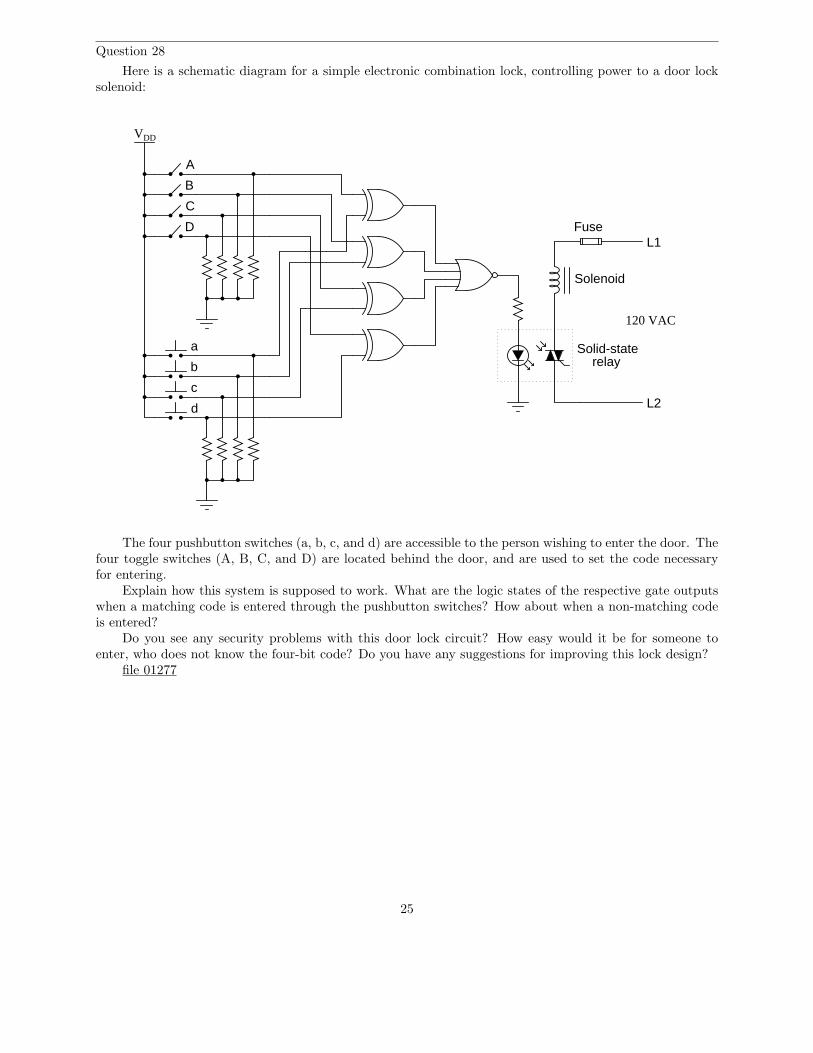
Here is a schematic diagram for a simple electronic combination lock, controlling power to a door locksolenoid:
VDD
L1
L2
120 VAC
Solenoid
A
B
C
D
a
b
c
d
Fuse
Solid-staterelay
The four pushbutton switches (a, b, c, and d) are accessible to the person wishing to enter the door. Thefour toggle switches (A, B, C, and D) are located behind the door, and are used to set the code necessaryfor entering.
Explain how this system is supposed to work. What are the logic states of the respective gate outputswhen a matching code is entered through the pushbutton switches? How about when a non-matching codeis entered?
Do you see any security problems with this door lock circuit? How easy would it be for someone toenter, who does not know the four-bit code? Do you have any suggestions for improving this lock design?
file 01277
25
Question 29
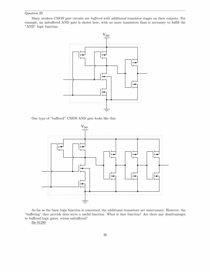
Many modern CMOS gate circuits are buffered with additional transistor stages on their outputs. Forexample, an unbuffered AND gate is shown here, with no more transistors than is necessary to fulfill the”AND” logic function:
VDD
One type of ”buffered” CMOS AND gate looks like this:
VDD
As far as the basic logic function is concerned, the additional transistors are unnecessary. However, the”buffering” they provide does serve a useful function. What is that function? Are there any disadvantagesto buffered logic gates, versus unbuffered?
file 01280
26
Question 30
In the early days of solid-state logic gate circuit technology, there was a very clear distinction betweenTTL and CMOS. TTL gates were capable of switching on and off very fast, required a tightly regulatedpower supply voltage, and used a lot of power. CMOS gates were not quite as fast as TTL, but could toleratea much wider range of power supply voltages and were far less wasteful on power.
Then, during the 1980’s a new technology known as high-speed CMOS, or HCMOS, entered the scene.Explain what HCMOS is, how it compares to the older TTL and CMOS families (54/74xx and 4xxx numberseries, respectively), and where it is often used. Hint: high-speed CMOS bears the same numerical codes asthe old TTL 54xx and 74xx series ICs (e.g. 74HC00 instead of 7400).
file 02773
Question 31
Though many electronics students and professionals alike associate semiconductor components with theword ”digital,” electromechanical relays are also digital logic (on or off) devices. In fact, some of the firstdigital computers were built with electromechanical relays as their active elements.
In what ways are electromechanical relays similar to semiconductor logic gates? In what ways do thetwo digital technologies differ?
file 01287
Question 32
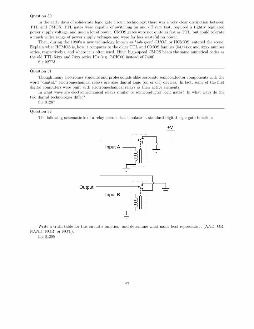
The following schematic is of a relay circuit that emulates a standard digital logic gate function:
+V
Input A
Input B
Output
Write a truth table for this circuit’s function, and determine what name best represents it (AND, OR,NAND, NOR, or NOT).
file 01288
27
Question 33
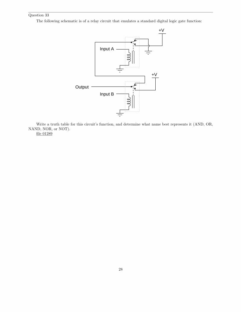
The following schematic is of a relay circuit that emulates a standard digital logic gate function:
+V
Input A
Input B
Output
+V
Write a truth table for this circuit’s function, and determine what name best represents it (AND, OR,NAND, NOR, or NOT).
file 01289
28
Question 34
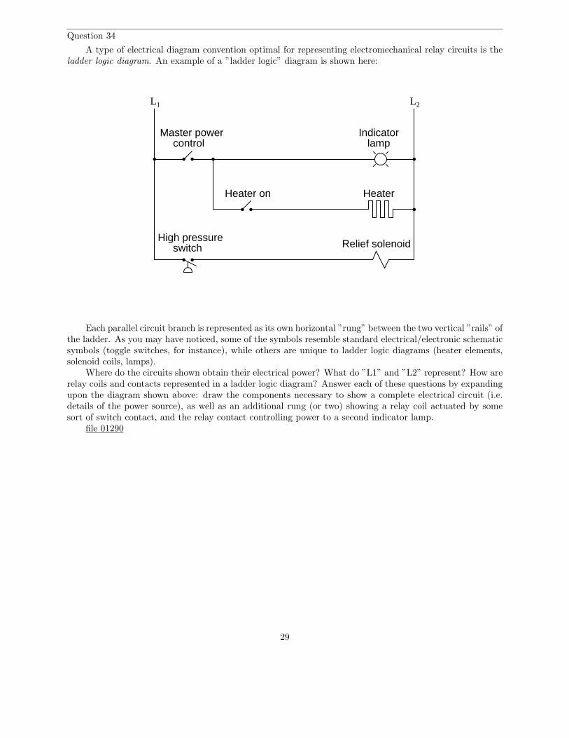
A type of electrical diagram convention optimal for representing electromechanical relay circuits is theladder logic diagram. An example of a ”ladder logic” diagram is shown here:
L1 L2
Indicatorlamp
HeaterHeater on
Master powercontrol
High pressureswitch Relief solenoid
Each parallel circuit branch is represented as its own horizontal ”rung” between the two vertical ”rails” ofthe ladder. As you may have noticed, some of the symbols resemble standard electrical/electronic schematicsymbols (toggle switches, for instance), while others are unique to ladder logic diagrams (heater elements,solenoid coils, lamps).
Where do the circuits shown obtain their electrical power? What do ”L1” and ”L2” represent? How arerelay coils and contacts represented in a ladder logic diagram? Answer each of these questions by expandingupon the diagram shown above: draw the components necessary to show a complete electrical circuit (i.e.details of the power source), as well as an additional rung (or two) showing a relay coil actuated by somesort of switch contact, and the relay contact controlling power to a second indicator lamp.
file 01290
29
Question 35
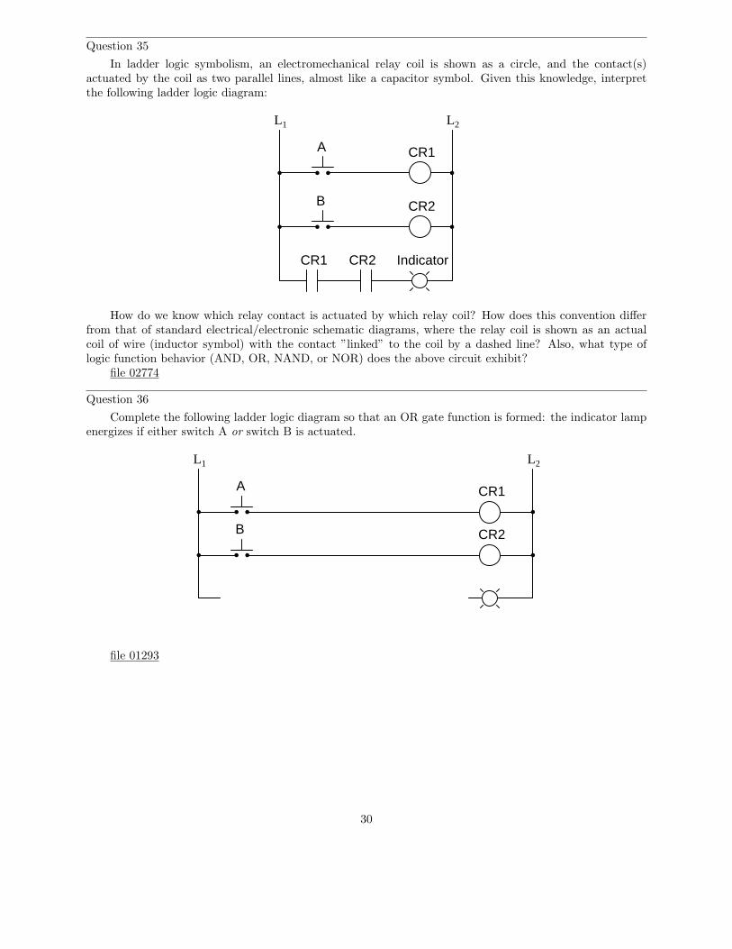
In ladder logic symbolism, an electromechanical relay coil is shown as a circle, and the contact(s)actuated by the coil as two parallel lines, almost like a capacitor symbol. Given this knowledge, interpretthe following ladder logic diagram:
L1 L2
A CR1
CR2B
CR1 CR2 Indicator
How do we know which relay contact is actuated by which relay coil? How does this convention differfrom that of standard electrical/electronic schematic diagrams, where the relay coil is shown as an actualcoil of wire (inductor symbol) with the contact ”linked” to the coil by a dashed line? Also, what type oflogic function behavior (AND, OR, NAND, or NOR) does the above circuit exhibit?
file 02774
Question 36
Complete the following ladder logic diagram so that an OR gate function is formed: the indicator lampenergizes if either switch A or switch B is actuated.
L1 L2
CR1A
B CR2
file 01293
30
Question 37
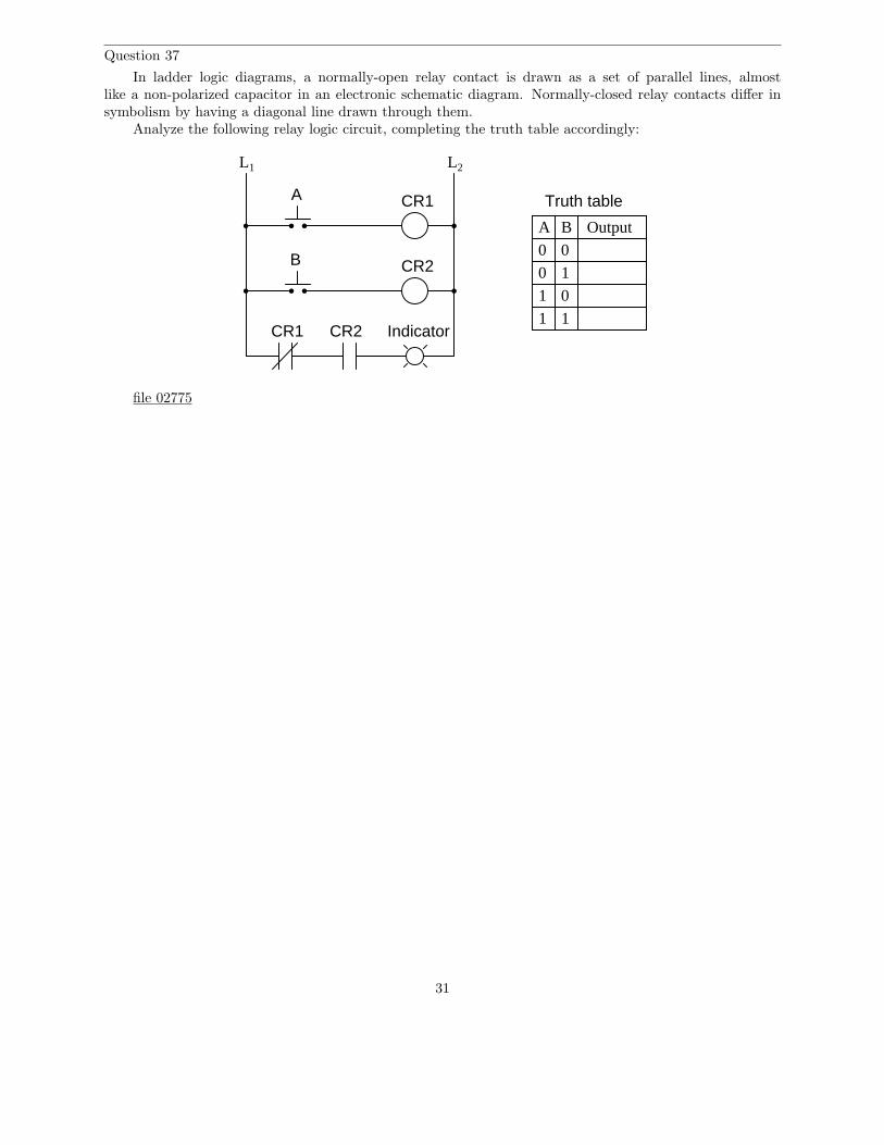
In ladder logic diagrams, a normally-open relay contact is drawn as a set of parallel lines, almostlike a non-polarized capacitor in an electronic schematic diagram. Normally-closed relay contacts differ insymbolism by having a diagonal line drawn through them.
Analyze the following relay logic circuit, completing the truth table accordingly:
L1 L2
A CR1
CR2B
CR1 CR2 Indicator
A B Output
00
0 1
01
1 1
Truth table
file 02775
31
Question 38
Identify each of these relay logic functions by name (AND, OR, NOR, etc.) and complete their respectivetruth tables:
A B Output
00
0 1
01
1 1
A B Output
00
0 1
01
1 1
A B Output
00
0 1
01
1 1
A B Output
00
0 1
01
1 1
A B Output
00
0 1
01
1 1
A B Output
00
0 1
01
1 1
A B Output
00
0 1
01
1 1
A B Output
00
0 1
01
1 1
A Output
A
BA B
A
B
CR1
CR1
A B CR1
CR1A B
A
B
A B
A B
A B
A B
A CR1
CR1
1
0
file 01335
32
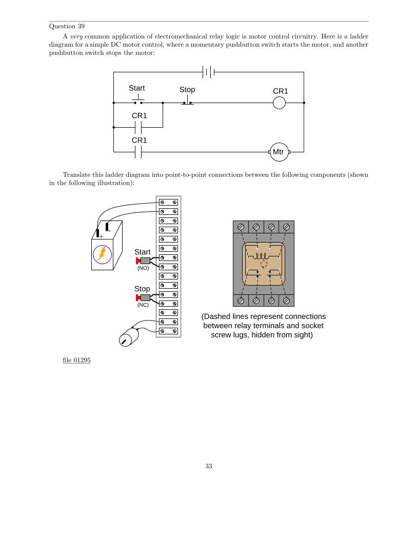
Question 39
A very common application of electromechanical relay logic is motor control circuitry. Here is a ladderdiagram for a simple DC motor control, where a momentary pushbutton switch starts the motor, and anotherpushbutton switch stops the motor:
CR1Start
CR1
Mtr
Stop
CR1
Translate this ladder diagram into point-to-point connections between the following components (shownin the following illustration):
+-
Start
Stop
(NO)
(NC)
(Dashed lines represent connectionsbetween relay terminals and socket
screw lugs, hidden from sight)
file 01295
33
Question 40
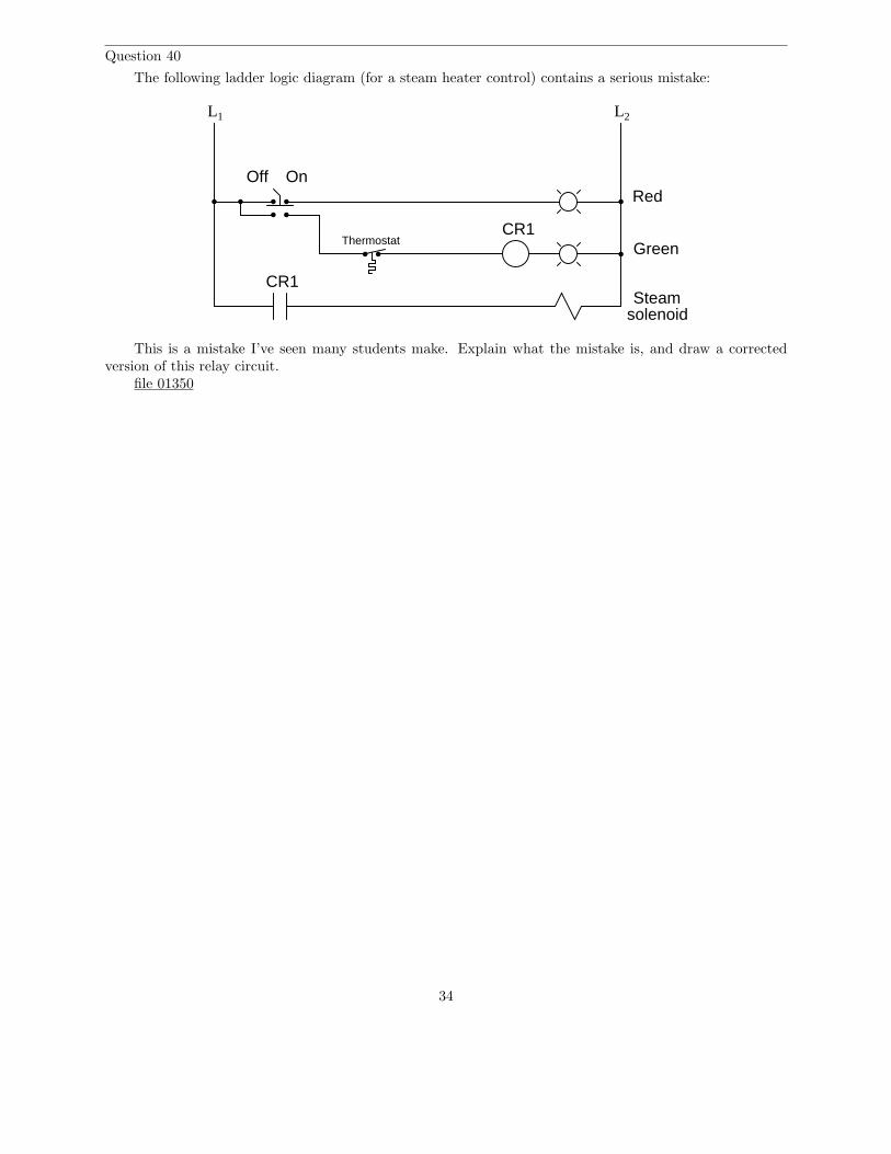
The following ladder logic diagram (for a steam heater control) contains a serious mistake:
L1 L2
Off OnRed
GreenCR1
CR1Steam
solenoid
Thermostat
This is a mistake I’ve seen many students make. Explain what the mistake is, and draw a correctedversion of this relay circuit.
file 01350
34
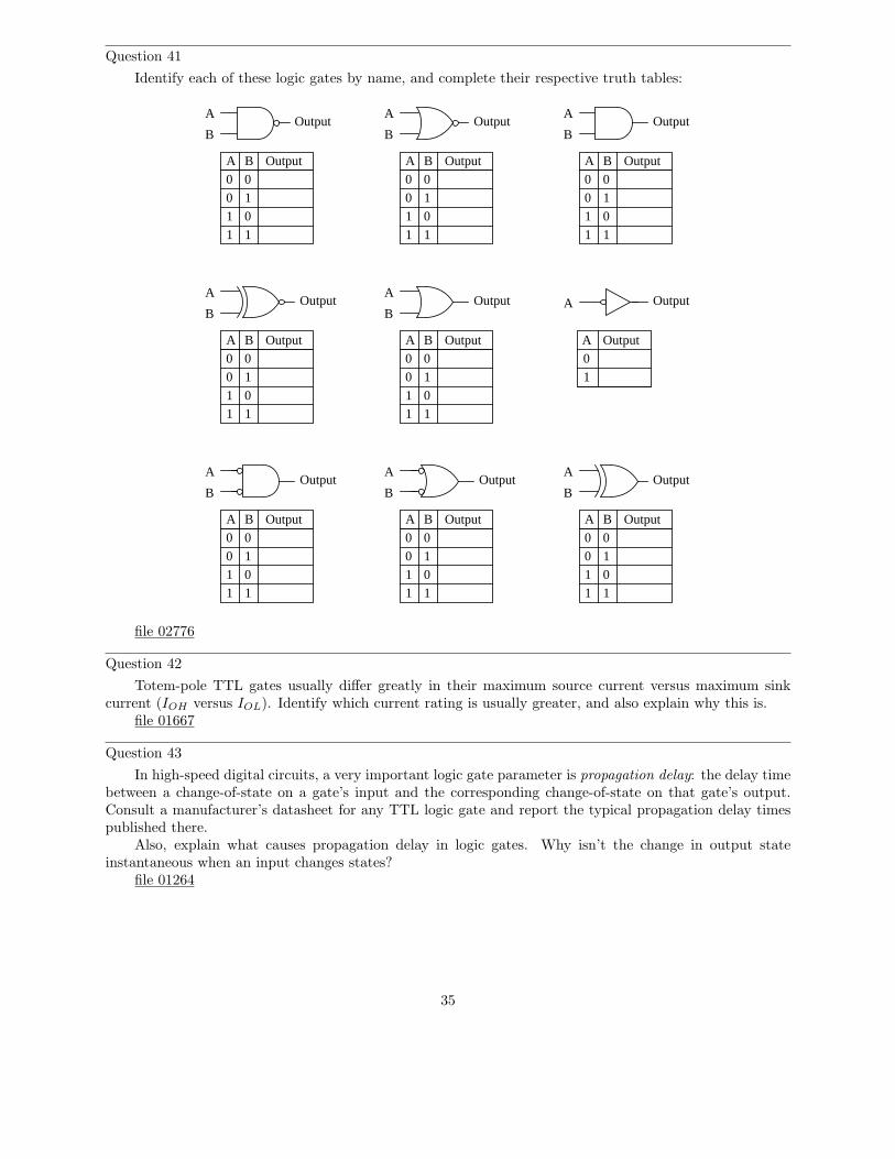
Question 41
Identify each of these logic gates by name, and complete their respective truth tables:
A B Output
00
0 1
01
1 1
A
BOutput
A B Output
00
0 1
01
1 1
A
BOutput
A B Output
00
0 1
01
1 1
A
BOutput
A B Output
00
0 1
01
1 1
A
BOutput
A B Output
00
0 1
01
1 1
A
BOutput
A B Output
00
0 1
01
1 1
A
BOutput
A B Output
00
0 1
01
1 1
A
BOutput
A B Output
00
0 1
01
1 1
A
BOutput A Output
A Output
0
1
file 02776
Question 42
Totem-pole TTL gates usually differ greatly in their maximum source current versus maximum sinkcurrent (IOH versus IOL). Identify which current rating is usually greater, and also explain why this is.
file 01667
Question 43
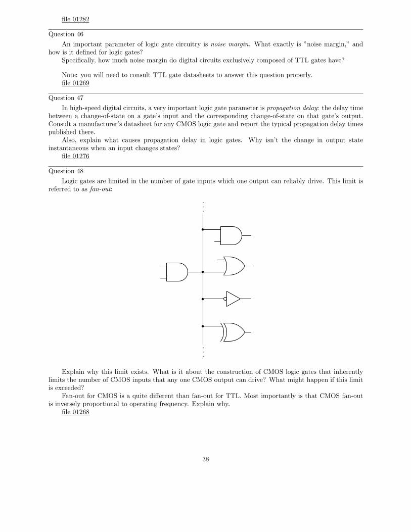
In high-speed digital circuits, a very important logic gate parameter is propagation delay: the delay timebetween a change-of-state on a gate’s input and the corresponding change-of-state on that gate’s output.Consult a manufacturer’s datasheet for any TTL logic gate and report the typical propagation delay timespublished there.
Also, explain what causes propagation delay in logic gates. Why isn’t the change in output stateinstantaneous when an input changes states?
file 01264
35
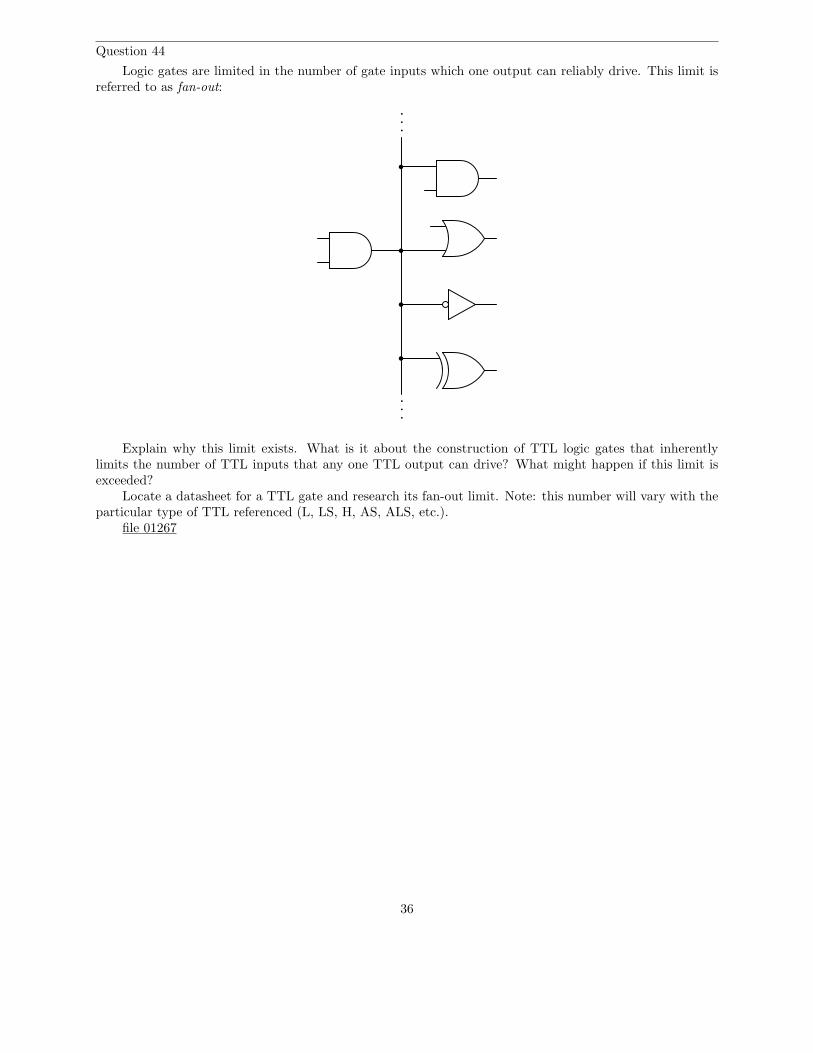
Question 44
Logic gates are limited in the number of gate inputs which one output can reliably drive. This limit isreferred to as fan-out:
. . .. . .
Explain why this limit exists. What is it about the construction of TTL logic gates that inherentlylimits the number of TTL inputs that any one TTL output can drive? What might happen if this limit isexceeded?
Locate a datasheet for a TTL gate and research its fan-out limit. Note: this number will vary with theparticular type of TTL referenced (L, LS, H, AS, ALS, etc.).
file 01267
36
Question 45
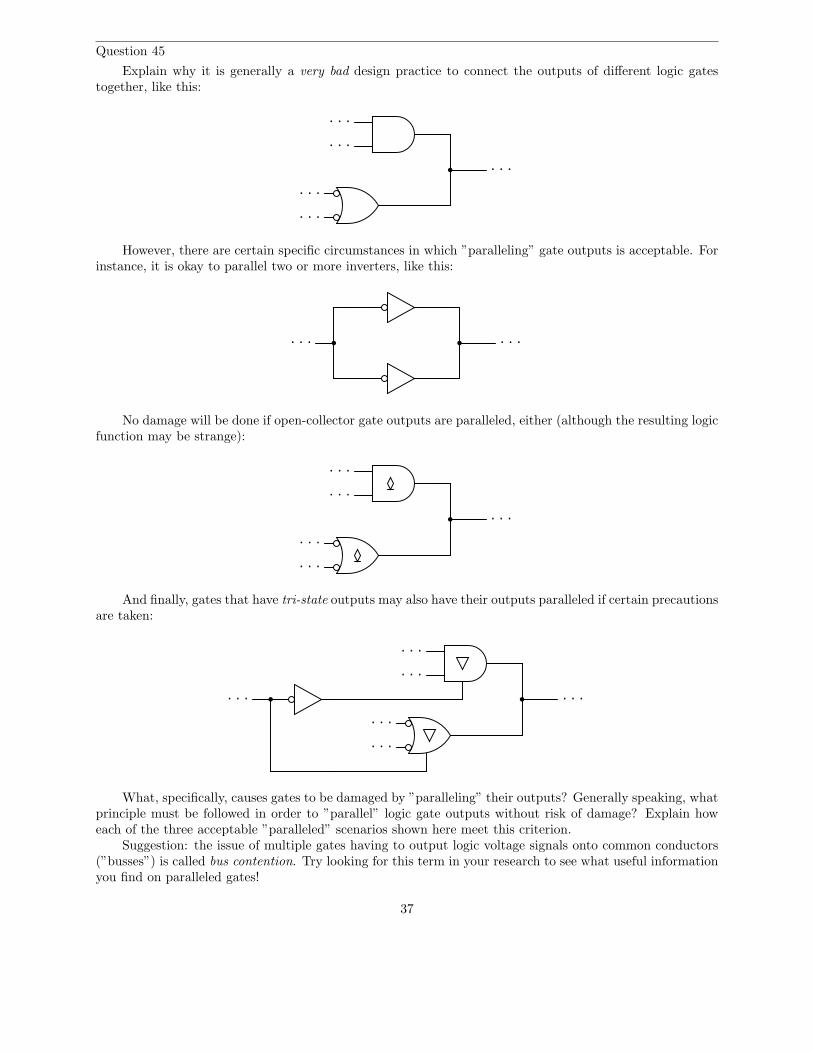
Explain why it is generally a very bad design practice to connect the outputs of different logic gatestogether, like this:
. . .
. . .
. . .
. . .
. . .
However, there are certain specific circumstances in which ”paralleling” gate outputs is acceptable. Forinstance, it is okay to parallel two or more inverters, like this:
. . .. . .
No damage will be done if open-collector gate outputs are paralleled, either (although the resulting logicfunction may be strange):
. . .
. . .
. . .
. . .
. . .
And finally, gates that have tri-state outputs may also have their outputs paralleled if certain precautionsare taken:
. . .
. . .
. . .
. . .
. . .. . .
What, specifically, causes gates to be damaged by ”paralleling” their outputs? Generally speaking, whatprinciple must be followed in order to ”parallel” logic gate outputs without risk of damage? Explain howeach of the three acceptable ”paralleled” scenarios shown here meet this criterion.
Suggestion: the issue of multiple gates having to output logic voltage signals onto common conductors(”busses”) is called bus contention. Try looking for this term in your research to see what useful informationyou find on paralleled gates!
37
file 01282
Question 46
An important parameter of logic gate circuitry is noise margin. What exactly is ”noise margin,” andhow is it defined for logic gates?
Specifically, how much noise margin do digital circuits exclusively composed of TTL gates have?
Note: you will need to consult TTL gate datasheets to answer this question properly.file 01269
Question 47
In high-speed digital circuits, a very important logic gate parameter is propagation delay: the delay timebetween a change-of-state on a gate’s input and the corresponding change-of-state on that gate’s output.Consult a manufacturer’s datasheet for any CMOS logic gate and report the typical propagation delay timespublished there.
Also, explain what causes propagation delay in logic gates. Why isn’t the change in output stateinstantaneous when an input changes states?
file 01276
Question 48
Logic gates are limited in the number of gate inputs which one output can reliably drive. This limit isreferred to as fan-out:
. . .. . .
Explain why this limit exists. What is it about the construction of CMOS logic gates that inherentlylimits the number of CMOS inputs that any one CMOS output can drive? What might happen if this limitis exceeded?
Fan-out for CMOS is a quite different than fan-out for TTL. Most importantly is that CMOS fan-outis inversely proportional to operating frequency. Explain why.
file 01268
38
Question 49
An important parameter of logic gate circuitry is noise margin. What exactly is ”noise margin,” andhow is it defined for logic gates?
Specifically, how much noise margin do digital circuits exclusively composed of CMOS gates have? Howdoes this compare with the noise margin of all-TTL circuitry?
Note: you will need to consult CMOS gate datasheets to answer this question properly.file 01270
Question 50
A trend in CMOS logic gate development is toward lower and lower operating voltages. The ”AUC”family of CMOS logic, for example, is able to operate at less than 2 volts VDD!
Explain why this is a trend in modern logic circuit design. What benefits result from lower operatingvoltages? What possible disadvantages also result?
file 01279
39
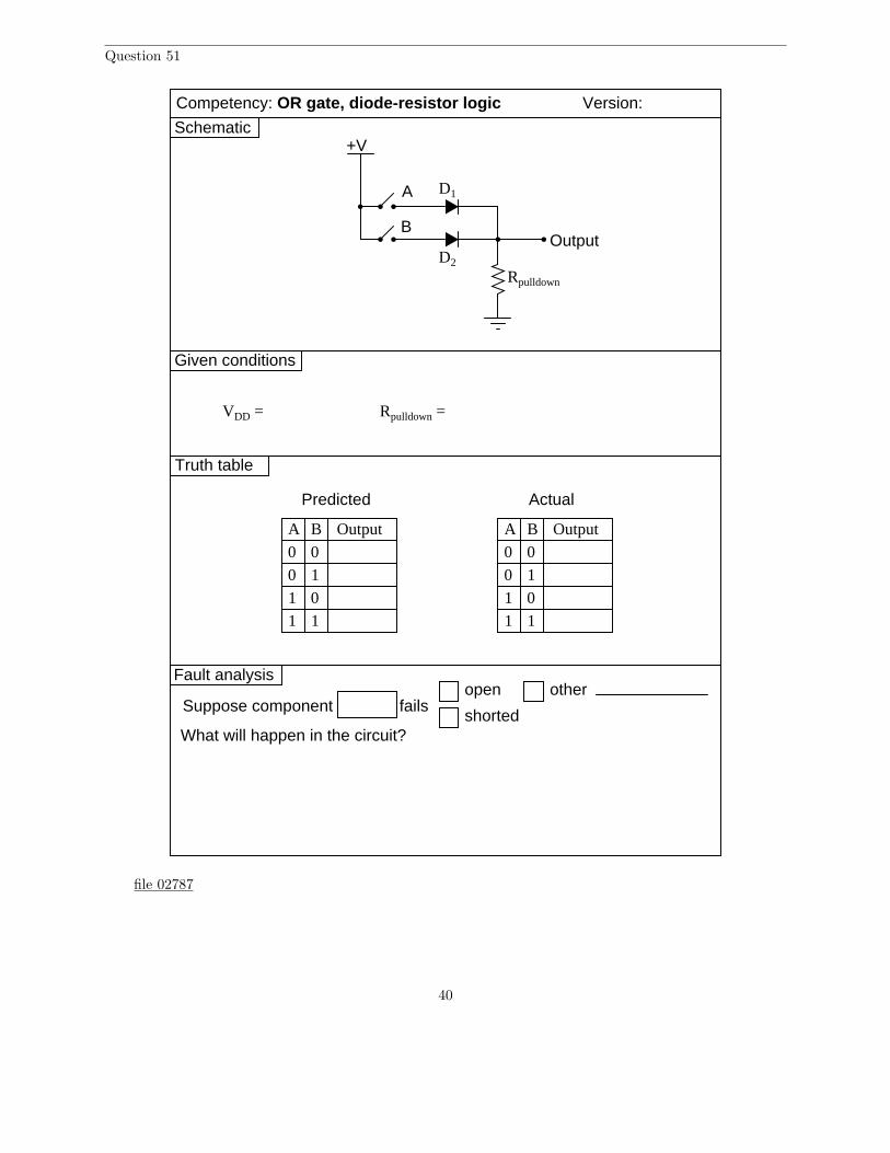
Question 51
Version:
Schematic
Truth table
A
B
Predicted Actual
Output
D1
D2
Competency: OR gate, diode-resistor logic
A B Output
00
0 1
01
1 1
A B Output
00
0 1
01
1 1
Given conditions
VDD = Rpulldown =
Rpulldown
+V
Fault analysis
Suppose component fails open
shorted
other
What will happen in the circuit?
file 02787
40
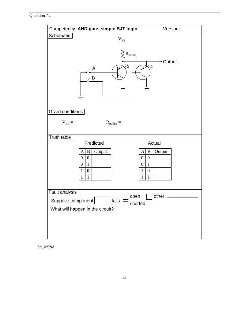
Question 52
Version:
Schematic
Truth table
A
B
Predicted Actual
Output
A B Output
00
0 1
01
1 1
A B Output
00
0 1
01
1 1
Given conditions
Rpullup
Rpullup =
Competency: AND gate, simple BJT logic
VEE
Q1 Q2
VEE =
Fault analysis
Suppose component fails open
shorted
other
What will happen in the circuit?
file 02793
41
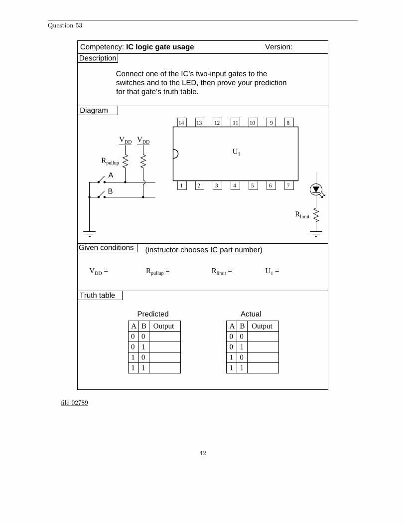
Question 53
Version:
Truth table
A
B
Predicted Actual
VDD VDD
Rpullup
Given conditions
VDD = Rpullup = Rlimit =
Rlimit
Competency: IC logic gate usage
14 13 12 11 10 9 8
7654321
Diagram
A B Output
00
0 1
01
1 1
A B Output
00
0 1
01
1 1
Description
Connect one of the IC’s two-input gates to theswitches and to the LED, then prove your predictionfor that gate’s truth table.
U1 =
U1
(instructor chooses IC part number)
file 02789
42
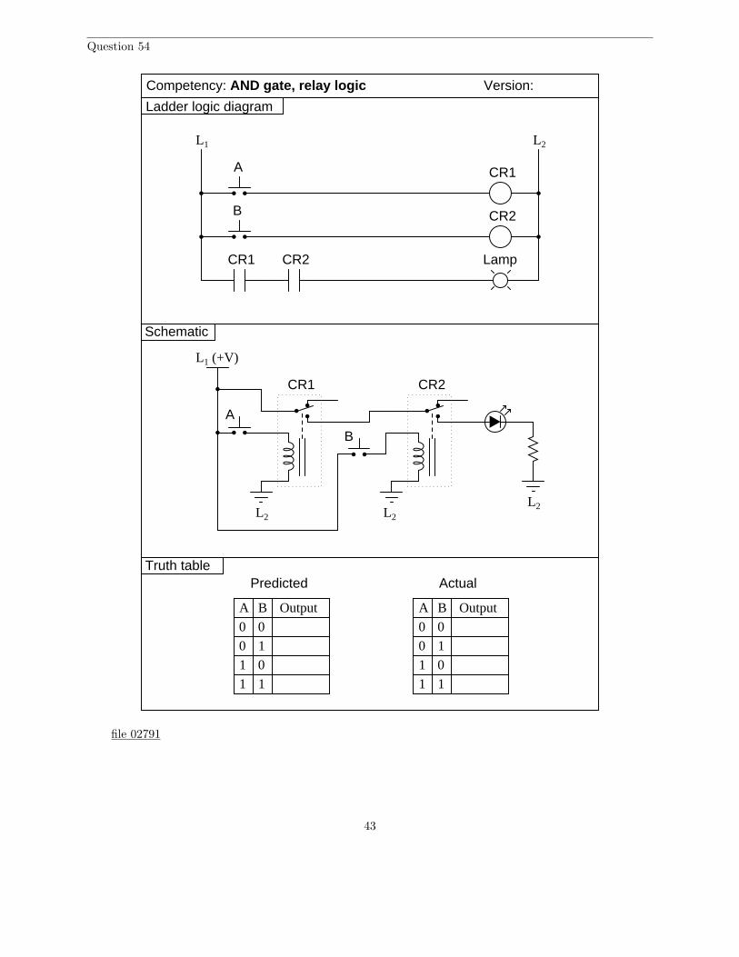
Question 54
Version:
Schematic
Truth tablePredicted Actual
A B Output
00
0 1
01
1 1
A B Output
00
0 1
01
1 1
Competency: AND gate, relay logic
Ladder logic diagram
L1 L2
A CR1
B CR2
CR1 CR2 Lamp
L2 L2
A
B
L2
CR1 CR2
L1 (+V)
file 02791
43

Question 55
Version:
Schematic
Truth table
A
B
Predicted Actual
A B Output
00
0 1
01
1 1
A B Output
00
0 1
01
1 1
Given conditions
Q1
Competency: Gate-relay interposing
+V
+V
+V
CR1
D1
U1
R1 R2
R3
+V = R1 = R2 = R3 =
Mtr
Fault analysis
Suppose component fails open
shorted
other
What will happen in the circuit?
file 02795
44

Question 56
NAME: Project Grading Criteria PROJECT:You will receive the highest score for which all criteria are met.
100 % (Must meet or exceed all criteria listed)A. Impeccable craftsmanship, comparable to that of a professional assemblyB. No spelling or grammatical errors anywhere in any document, upon first submission to instructor
95 % (Must meet or exceed these criteria in addition to all criteria for 90% and below)A. Technical explanation sufficiently detailed to teach from, inclusive of every component (supersedes 75.B)B. Itemized parts list complete with part numbers, manufacturers, and (equivalent) prices for all
components, including recycled components and parts kit components (supersedes 90.A)
90 % (Must meet or exceed these criteria in addition to all criteria for 85% and below)A. Itemized parts list complete with prices of components purchased for the project, plus total priceB. No spelling or grammatical errors anywhere in any document upon final submission
85 % (Must meet or exceed these criteria in addition to all criteria for 80% and below)A. “User’s guide” to project function (in addition to 75.B)B. Troubleshooting log describing all obstacles overcome during development and construction
80 % (Must meet or exceed these criteria in addition to all criteria for 75% and below)A. All controls (switches, knobs, etc.) clearly and neatly labeledB. All documentation created on computer, not hand-written (including the schematic diagram)
75 % (Must meet or exceed these criteria in addition to all criteria for 70% and below)A. Stranded wire used wherever wires are subject to vibration or bendingB. Basic technical explanation of all major circuit sectionsC. Deadline met for working prototype of circuit (Date/Time = / )
70 % (Must meet or exceed these criteria in addition to all criteria for 65%)A. All wire connections sound (solder joints, wire-wrap, terminal strips, and lugs are all connected properly)B. No use of glue where a fastener would be more appropriateC. Deadline met for submission of fully-functional project (Date/Time = / ) –
supersedes 75.C if final project submitted by that (earlier) deadline
65 % (Must meet or exceed these criteria in addition to all criteria for 60%)A. Project fully functionalB. All components securely fastened so nothing is “loose” inside the enclosureC. Schematic diagram of circuit
60 % (Must meet or exceed these criteria in addition to being safe and legal)A. Project minimally functional, with all components located inside an enclosure (if applicable)B. Passes final safety inspection (proper case grounding, line power fusing, power cords strain-relieved)
0 % (If any of the following conditions are true)A. Fails final safety inspection (improper grounding, fusing, and/or power cord strain relieving)B. Intended project function poses a safety hazardC. Project function violates any law, ordinance, or school policy
file 03173
45
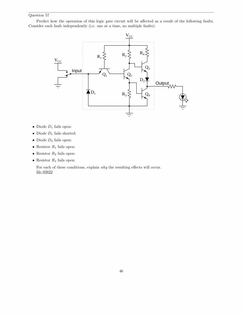
Question 57
Predict how the operation of this logic gate circuit will be affected as a result of the following faults.Consider each fault independently (i.e. one at a time, no multiple faults):
VCC
Input
Output
VCC
R1R2
R3
Q1 Q2
Q3
Q4D1
D2
R4
• Diode D1 fails open:
• Diode D1 fails shorted:
• Diode D2 fails open:
• Resistor R1 fails open:
• Resistor R2 fails open:
• Resistor R4 fails open:
For each of these conditions, explain why the resulting effects will occur.file 03822
46
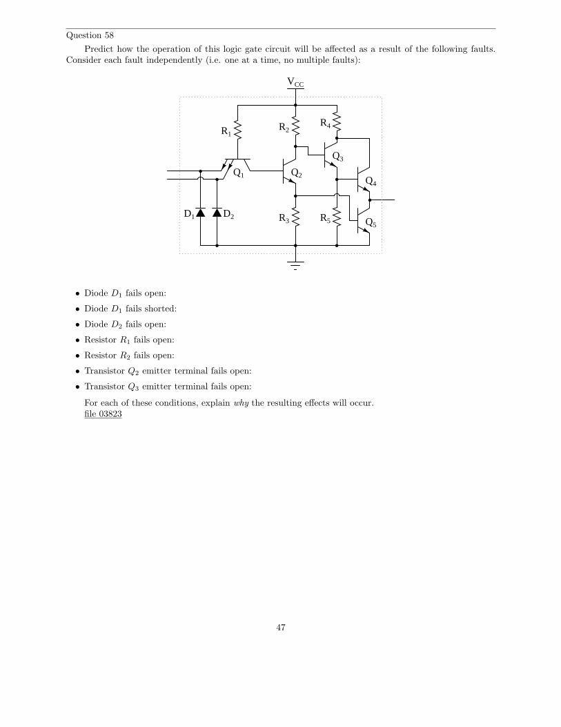
Question 58
Predict how the operation of this logic gate circuit will be affected as a result of the following faults.Consider each fault independently (i.e. one at a time, no multiple faults):
VCC
D1 D2
Q1
R1R2
R3
R4
R5
Q2
Q3
Q4
Q5
• Diode D1 fails open:
• Diode D1 fails shorted:
• Diode D2 fails open:
• Resistor R1 fails open:
• Resistor R2 fails open:
• Transistor Q2 emitter terminal fails open:
• Transistor Q3 emitter terminal fails open:
For each of these conditions, explain why the resulting effects will occur.file 03823
47
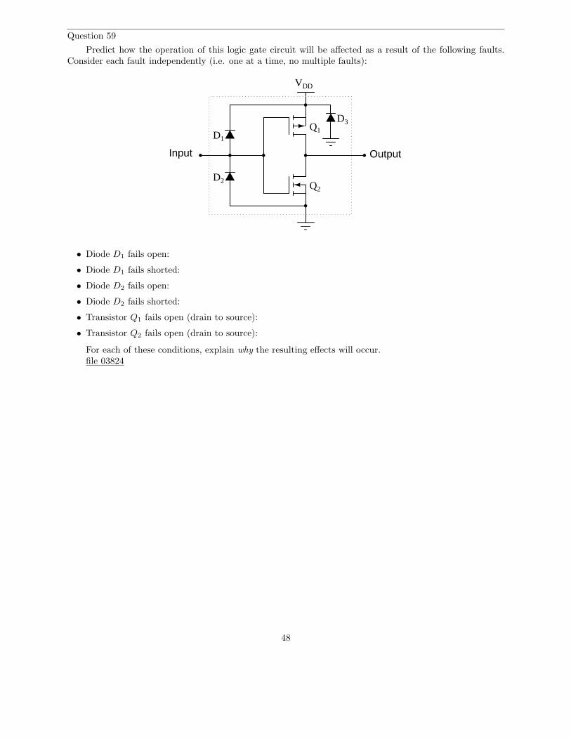
Question 59
Predict how the operation of this logic gate circuit will be affected as a result of the following faults.Consider each fault independently (i.e. one at a time, no multiple faults):
VDD
Input Output
D1
D2
D3Q1
Q2
• Diode D1 fails open:
• Diode D1 fails shorted:
• Diode D2 fails open:
• Diode D2 fails shorted:
• Transistor Q1 fails open (drain to source):
• Transistor Q2 fails open (drain to source):
For each of these conditions, explain why the resulting effects will occur.file 03824
48
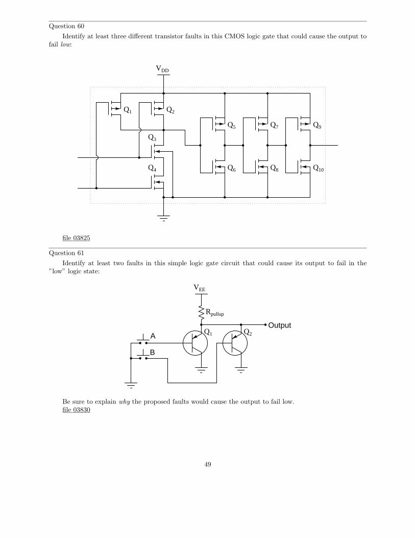
Question 60
Identify at least three different transistor faults in this CMOS logic gate that could cause the output tofail low:
VDD
Q1 Q2
Q3
Q4
Q5
Q6
Q7
Q8
Q9
Q10
file 03825
Question 61
Identify at least two faults in this simple logic gate circuit that could cause its output to fail in the”low” logic state:
A
B
Output
Rpullup
VEE
Q1 Q2
Be sure to explain why the proposed faults would cause the output to fail low.file 03830
49
Question 62
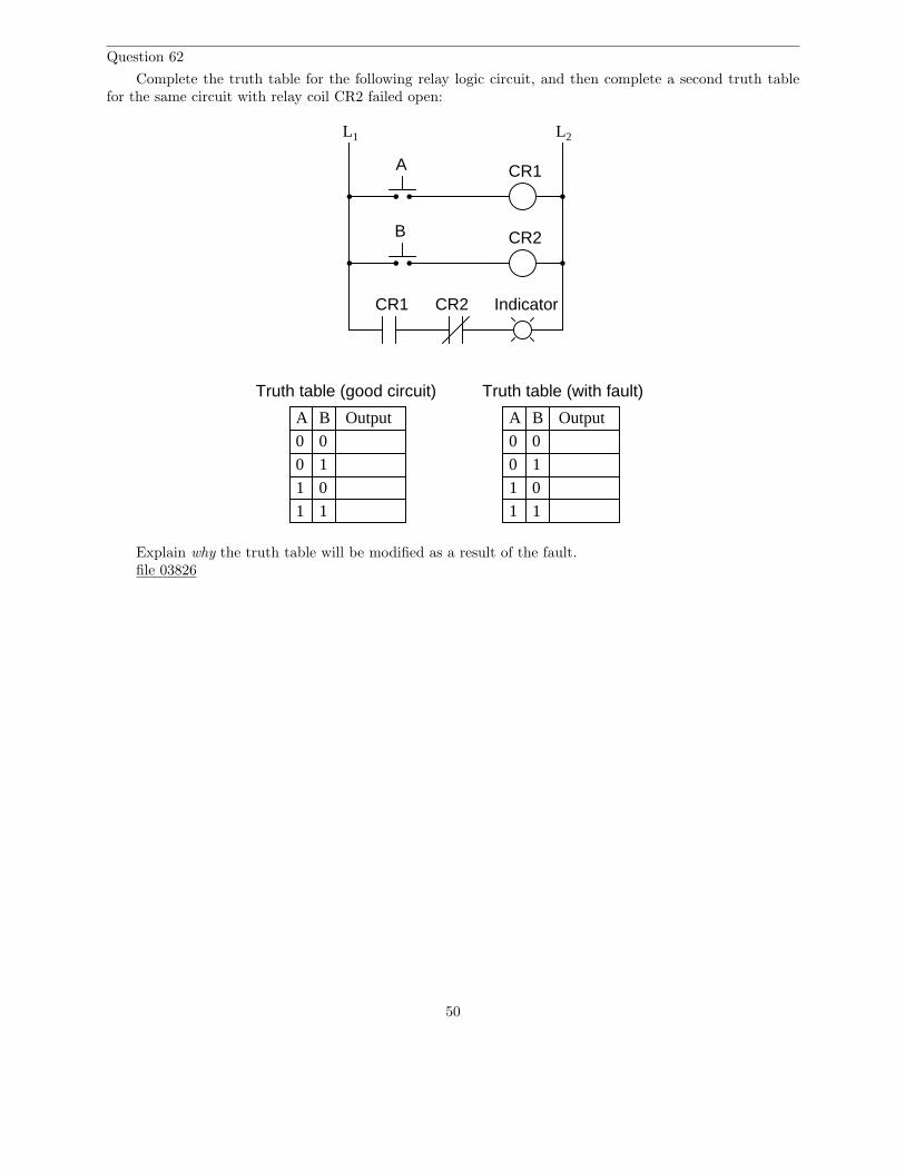
Complete the truth table for the following relay logic circuit, and then complete a second truth tablefor the same circuit with relay coil CR2 failed open:
L1 L2
A CR1
CR2B
CR1 CR2 Indicator
A B Output
00
0 1
01
1 1
A B Output
00
0 1
01
1 1
Truth table (good circuit) Truth table (with fault)
Explain why the truth table will be modified as a result of the fault.file 03826
50
Question 63
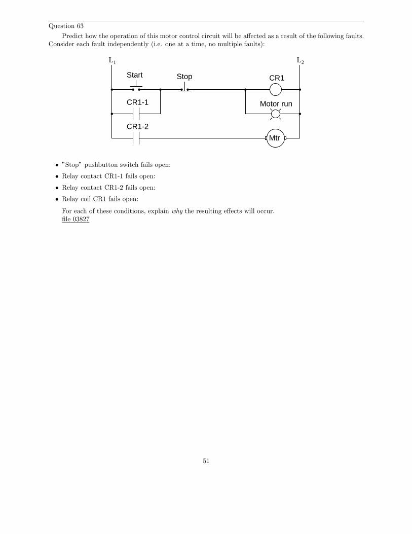
Predict how the operation of this motor control circuit will be affected as a result of the following faults.Consider each fault independently (i.e. one at a time, no multiple faults):
CR1Start
Mtr
Stop
L1 L2
CR1-1
CR1-2
Motor run
• ”Stop” pushbutton switch fails open:
• Relay contact CR1-1 fails open:
• Relay contact CR1-2 fails open:
• Relay coil CR1 fails open:
For each of these conditions, explain why the resulting effects will occur.file 03827
51
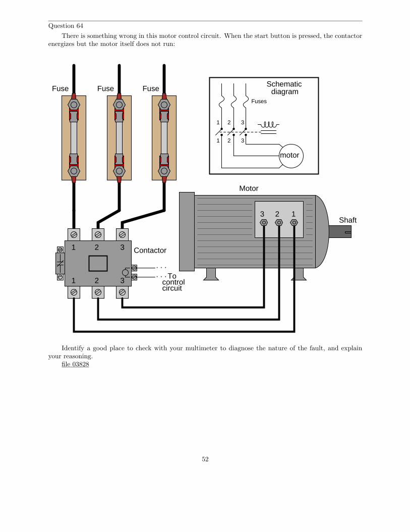
Question 64
There is something wrong in this motor control circuit. When the start button is pressed, the contactorenergizes but the motor itself does not run:
Fuse
Motor
Shaft
Fuse Fuse
1 2 3
1 2 3
Contactor
123
motor
Schematicdiagram
1 2 3
1 2 3
Fuses
Tocontrolcircuit
. . .
. . .
Identify a good place to check with your multimeter to diagnose the nature of the fault, and explainyour reasoning.
file 03828
52

Question 65
Identify at least three independent faults that could cause this motor not to start:
Motor
motor
Fuses
Contactor
Contactor
H1
H2
H3
H4
X1
X2
Transformer
X1 X2
H1 H2H3 H4
SwitchSwitch
Transformer
To 3-φ , 480 volt power source
Schematic diagramL1 L2 L3L1 L2 L3
T1 T2 T3
T1 T2 T3
A1A2
A1
A2
For each of the proposed faults, explain why they would prevent the motor from starting.file 03829
53
Question 66
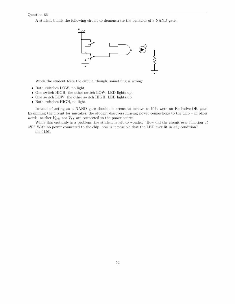
A student builds the following circuit to demonstrate the behavior of a NAND gate:
VDD
When the student tests the circuit, though, something is wrong:
• Both switches LOW, no light.• One switch HIGH, the other switch LOW; LED lights up.• One switch LOW, the other switch HIGH; LED lights up.• Both switches HIGH, no light.
Instead of acting as a NAND gate should, it seems to behave as if it were an Exclusive-OR gate!Examining the circuit for mistakes, the student discovers missing power connections to the chip – in otherwords, neither VDD nor VSS are connected to the power source.
While this certainly is a problem, the student is left to wonder, ”How did the circuit ever function atall?” With no power connected to the chip, how is it possible that the LED ever lit in any condition?
file 01561
54
Question 67
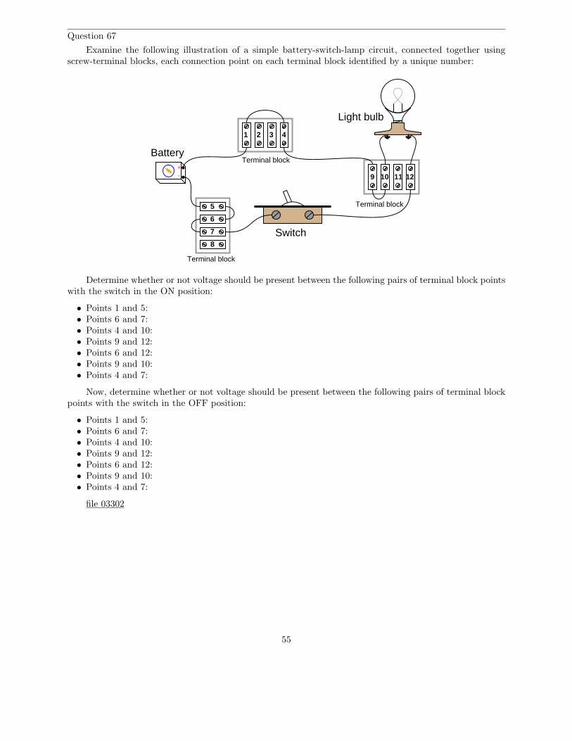
Examine the following illustration of a simple battery-switch-lamp circuit, connected together usingscrew-terminal blocks, each connection point on each terminal block identified by a unique number:
+-
Battery
Switch
1 2 3 4
Light bulb
5
6
7
8
9 10 11 12
Terminal block
Terminal block
Terminal block
Determine whether or not voltage should be present between the following pairs of terminal block pointswith the switch in the ON position:
• Points 1 and 5:• Points 6 and 7:• Points 4 and 10:• Points 9 and 12:• Points 6 and 12:• Points 9 and 10:• Points 4 and 7:
Now, determine whether or not voltage should be present between the following pairs of terminal blockpoints with the switch in the OFF position:
• Points 1 and 5:• Points 6 and 7:• Points 4 and 10:• Points 9 and 12:• Points 6 and 12:• Points 9 and 10:• Points 4 and 7:
file 03302
55
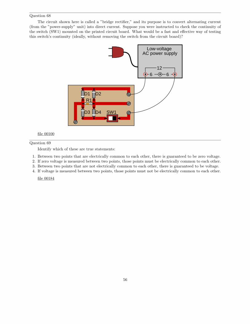
Question 68
The circuit shown here is called a ”bridge rectifier,” and its purpose is to convert alternating current(from the ”power-supply” unit) into direct current. Suppose you were instructed to check the continuity ofthe switch (SW1) mounted on the printed circuit board. What would be a fast and effective way of testingthis switch’s continuity (ideally, without removing the switch from the circuit board)?
SW1
D1 D2
D3 D4
Low-voltage AC power supply
6 612
R1
file 00100
Question 69
Identify which of these are true statements:
1. Between two points that are electrically common to each other, there is guaranteed to be zero voltage.2. If zero voltage is measured between two points, those points must be electrically common to each other.3. Between two points that are not electrically common to each other, there is guaranteed to be voltage.4. If voltage is measured between two points, those points must not be electrically common to each other.
file 00184
56
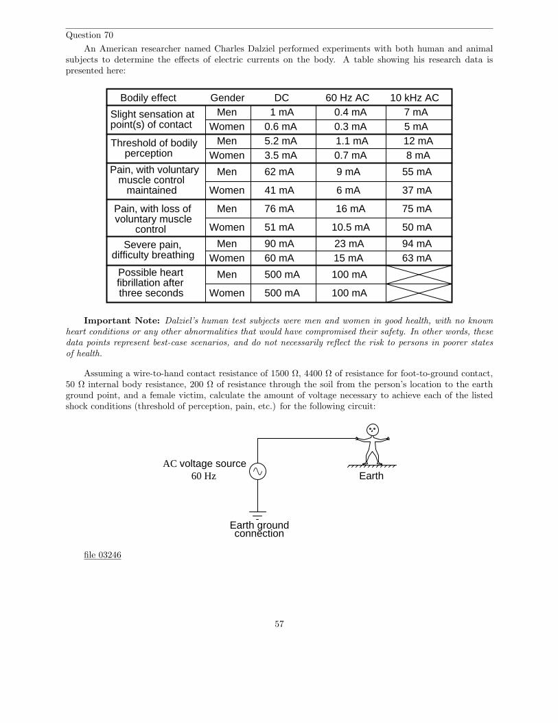
Question 70
An American researcher named Charles Dalziel performed experiments with both human and animalsubjects to determine the effects of electric currents on the body. A table showing his research data ispresented here:
Bodily effect 60 Hz AC 10 kHz AC
Slight sensation atpoint(s) of contact
Threshold of bodilyperception
Pain, with voluntarymuscle control
maintained
DC
Pain, with loss ofvoluntary muscle
control
Severe pain,difficulty breathing
Possible heartfibrillation afterthree seconds
MenWomen
Gender
MenWomen
Men
Women
Men
Women
MenWomen
Men
Women
1 mA0.6 mA
0.4 mA0.3 mA
7 mA5 mA
5.2 mA3.5 mA
1.1 mA0.7 mA
12 mA8 mA
62 mA
41 mA
9 mA
6 mA
55 mA
37 mA
16 mA
10.5 mA
76 mA
51 mA
75 mA
50 mA
90 mA60 mA
23 mA15 mA
94 mA63 mA
500 mA
500 mA
100 mA
100 mA
Important Note: Dalziel’s human test subjects were men and women in good health, with no knownheart conditions or any other abnormalities that would have compromised their safety. In other words, thesedata points represent best-case scenarios, and do not necessarily reflect the risk to persons in poorer statesof health.
Assuming a wire-to-hand contact resistance of 1500 Ω, 4400 Ω of resistance for foot-to-ground contact,50 Ω internal body resistance, 200 Ω of resistance through the soil from the person’s location to the earthground point, and a female victim, calculate the amount of voltage necessary to achieve each of the listedshock conditions (threshold of perception, pain, etc.) for the following circuit:
60 HzAC voltage source
Earth ground
Earth
connection
file 03246
57
Question 71
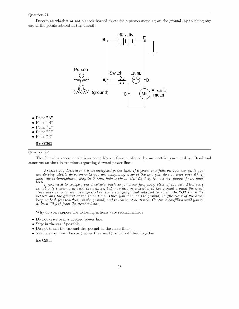
Determine whether or not a shock hazard exists for a person standing on the ground, by touching anyone of the points labeled in this circuit:
Person
Mtr
Switch Lamp
Electricmotor
230 volts
(ground)
A
B
C
D
E
• Point ”A”• Point ”B”• Point ”C”• Point ”D”• Point ”E”
file 00303
Question 72
The following recommendations came from a flyer published by an electric power utility. Read andcomment on their instructions regarding downed power lines:
Assume any downed line is an energized power line. If a power line falls on your car while youare driving, slowly drive on until you are completely clear of the line (but do not drive over it). Ifyour car is immobilized, stay in it until help arrives. Call for help from a cell phone if you haveone.
If you need to escape from a vehicle, such as for a car fire, jump clear of the car. Electricityis not only traveling through the vehicle, but may also be traveling in the ground around the area.Keep your arms crossed over your chest while you jump, and both feet together. Do NOT touch thevehicle and the ground at the same time. Once you land on the ground, shuffle clear of the area,keeping both feet together, on the ground, and touching at all times. Continue shuffling until you’reat least 30 feet from the accident site.
Why do you suppose the following actions were recommended?
• Do not drive over a downed power line.• Stay in the car if possible.• Do not touch the car and the ground at the same time.• Shuffle away from the car (rather than walk), with both feet together.
file 02911
58
Question 73
When securing equipment for safe maintenance, special tags are attached with the lock(s) used to keepcircuit breakers and other disconnect devices in the open (off) state. A typical ”lockout” tag looks somethinglike this:
DANGER
DONOT
OPERATE
Signed by
Date
What is the purpose of attaching such a tag to an electrical disconnect device in addition to locking itin the open position? Why is a lock, by itself, not sufficient from a safety perspective?
file 00573
Question 74
Suppose you are finishing a maintenance project where an electric motor was locked out and tagged,and now the work is complete. Your lock is the last one to be removed from the circuit breaker, everyone elsealready having taken their locks and tags off. What should you do before removing your lock and turningthe circuit breaker back on?
file 00575
Question 75
When engineers and physicists draw pictures illustrating the magnetic field produced by a straightcurrent-carrying wire, they usually do so using this notation:
I
wire
Explain what the circle-and-dot and circle-and-cross symbols mean, with reference to the right-handrule.
file 03498
59
Question 76
A very useful method of measuring current through a wire is to measure the strength of the magneticfield around it. This type of ammeter is known as a clamp-on ammeter:
magnetic fieldencircling the current-carryingconductor
clamp-onammeter
Current to bemeasured
(conventional flow)
Knowing the principle behind this meter’s operation, describe what current values will be indicated bythe three clamp-on ammeters in this circuit:
+-
+-
+-
+-
6 volts 6 volts 6 volts 6 volts
24 volts60 watts
Meter A
Meter B
Meter C
• Meter A =• Meter B =• Meter C =
file 00262
60

Question 77
Write an equation that expresses the amount of magnetic flux (Φ) produced by an electromagnet, giventhe amount of electric current (I), the number of turns in the wire coil (N), and the reluctance of the corematerial (ℜ).
file 00258
Question 78∫
f(x) dx Calculus alert!
Plot the relative B-H curves for a sample of air and a sample of iron, in proportion to each other (asmuch as possible):
B
H
Iron
Air
What do you notice about the slope (also called the derivative, or dBdH
) of each plot?file 03515
Question 79
If a wire coil with 450 turns is exposed to a magnetic flux increasing at a rate of 0.008 Webers persecond, how much voltage will be induced across the coil?
450 turns
N S
file 01983
61
Question 80
Lenz’s Law describes the opposition to changes in magnetic flux resulting from electromagnetic inductionbetween a magnetic field and an electrical conductor. One apparatus capable of demonstrating Lenz’s Lawis a copper or aluminum disk (electrically conductive, but non-magnetic) positioned close to the end of apowerful permanent magnet. There is no attraction or repulsion between the disk and magnet when there isno motion, but a force will develop between the two objects if either is suddenly moved. This force will be insuch a direction that it tries to resist the motion (i.e. the force tries to maintain the gap constant betweenthe two objects):
N S
Motion
Reactionforce
We know this force is magnetic in nature. That is, the induced current causes the disk itself to become amagnet in order to react against the permanent magnet’s field and produce the opposing force. For each ofthe following scenarios, label the disk’s induced magnetic poles (North and South) as it reacts to the motionimposed by an outside force:
N S
Motion
N S
Motion
Figure 1 Figure 2
Figure 3 Figure 4
NS
Motion
NS
Motion
file 01982
62
Question 81
Combining Lenz’s Law with the right-hand rule (or left-hand rule, if you follow electron flow instead ofconventional flow) provides a simple and effective means for determining the direction of induced current inan induction coil. In the following examples, trace the direction of current through the load resistor:
Figure 1 Figure 2 Figure 3
Figure 4 Figure 5 Figure 6
NS
MotionNS
Motion
NS
Motion
NS
Motion
NS
Motion
NS
Motion
file 01787
63
Question 82
Apply the following terms to this graph of an AC voltage measured over time:
• Frequency• Period• Hertz• Amplitude
Time0 10 ms 20 ms 30 ms 40 ms
+5 V
+10 V
-5 V
-10 V
0 V
file 00054
Question 83
Radio waves are comprised of oscillating electric and magnetic fields, which radiate away from sourcesof high-frequency AC at (nearly) the speed of light. An important measure of a radio wave is its wavelength,defined as the distance the wave travels in one complete cycle.
Suppose a radio transmitter operates at a fixed frequency of 950 kHz. Calculate the approximatewavelength (λ) of the radio waves emanating from the transmitter tower, in the metric distance unit ofmeters. Also, write the equation you used to solve for λ.
file 01819
64
Question 84
Determine the RMS amplitude of this sinusoidal waveform, as displayed by an oscilloscope with a verticalsensitivity of 0.2 volts per division:
file 01818
Question 85
Determine the RMS voltage (amplitude) of this square-wave signal, as displayed by an oscilloscope witha vertical sensitivity of 0.5 volts per division:
file 01824
65
Question 86
Calculate the amount of phase shift indicated by this Lissajous figure:
file 03577
Question 87
Read the following quotation, and then research the term microcontroller to see what relevance it hasto the quote:
I went to my first computer conference at the New York Hilton about 20 years ago. When somebodythere predicted the market for microprocessors would eventually be in the millions, someone elsesaid, “Where are they all going to go? It’s not like you need a computer in every doorknob!”
Years later, I went back to the same hotel. I noticed the room keys had been replaced by electroniccards you slide into slots in the doors.
There was a computer in every doorknob.
– Danny Hillis
file 02581
66
Question 88
A microcontroller unit, or MCU, is a specialized type of digital computer used to provide automaticsequencing or control of a system. Microcontrollers differ from ordinary digital computers in being verysmall (typically a single integrated circuit chip), with several dedicated pins for input and/or output ofdigital signals, and limited memory. Instructions programmed into the microcontroller’s memory tell it howto react to input conditions, and what types of signals to send to the outputs.
The simplest type of signal ”understood” by a microcontroller is a discrete voltage level: either ”high”(approximately +V) or ”low” (approximately ground potential) measured at a specified pin on the chip.Transistors internal to the microcontroller produce these ”high” and ”low” signals at the output pins, theiractions being modeled by SPDT switches for simplicity’s sake:
Microcontroller
DCpowersource
+V
Gnd
. . .
+V
Gnd
+V
Gnd
+V
Gnd
Each output "switch"controlled by instructions
contained in memory
. . .
Input signals actedupon by instructionscontained in memory
Programmedinstructions
Input pin 0
Input pin 1
Input pin n
Output pin 0
Output pin 1
Output pin n
Microcontrollers may be programmed to emulate the functions of digital logic gates (AND, OR, NAND,NOR, etc.) in addition to a wide variety of combinational and multivibrator functions. The only real limitsto what a microcontroller can do are memory (how large of a program may be stored) and input/outputpins on the MCU chip.
However, microcontrollers are themselves made up of many thousands (or millions!) of logic gatecircuits. Why would it make sense to use a microcontroller to perform a logic function that a small fractionof its constituent gates could accomplish directly? In other words, why would anyone bother to program amicrocontroller to perform a digital function when they could build the logic network they needed out offewer gate circuits?
file 02596
67
Question 89
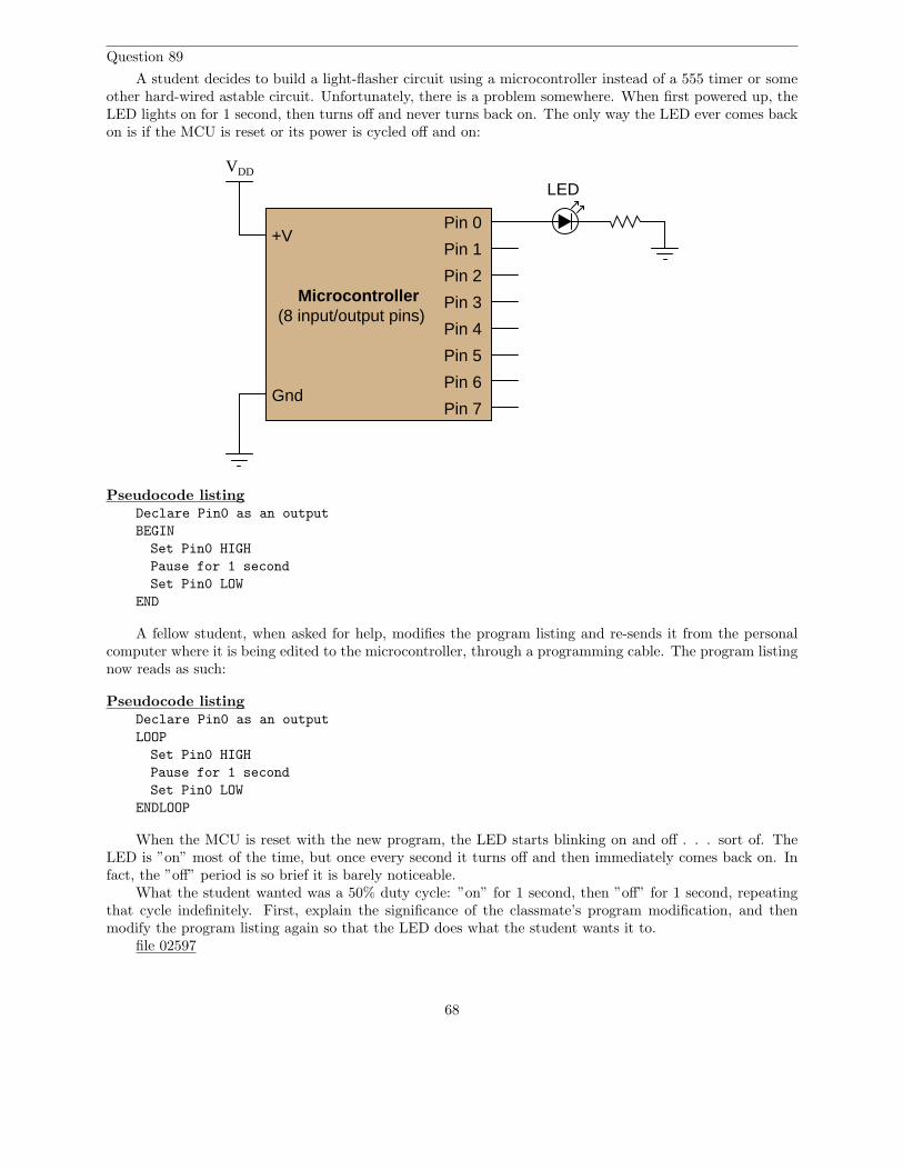
A student decides to build a light-flasher circuit using a microcontroller instead of a 555 timer or someother hard-wired astable circuit. Unfortunately, there is a problem somewhere. When first powered up, theLED lights on for 1 second, then turns off and never turns back on. The only way the LED ever comes backon is if the MCU is reset or its power is cycled off and on:
Microcontroller
+V
Gnd
(8 input/output pins)
Pin 0
Pin 1
Pin 2
Pin 3
Pin 4
Pin 5
Pin 6
Pin 7
VDD
LED
Pseudocode listingDeclare Pin0 as an output
BEGIN
Set Pin0 HIGH
Pause for 1 second
Set Pin0 LOW
END
A fellow student, when asked for help, modifies the program listing and re-sends it from the personalcomputer where it is being edited to the microcontroller, through a programming cable. The program listingnow reads as such:
Pseudocode listingDeclare Pin0 as an output
LOOP
Set Pin0 HIGH
Pause for 1 second
Set Pin0 LOW
ENDLOOP
When the MCU is reset with the new program, the LED starts blinking on and off . . . sort of. TheLED is ”on” most of the time, but once every second it turns off and then immediately comes back on. Infact, the ”off” period is so brief it is barely noticeable.
What the student wanted was a 50% duty cycle: ”on” for 1 second, then ”off” for 1 second, repeatingthat cycle indefinitely. First, explain the significance of the classmate’s program modification, and thenmodify the program listing again so that the LED does what the student wants it to.
file 02597
68
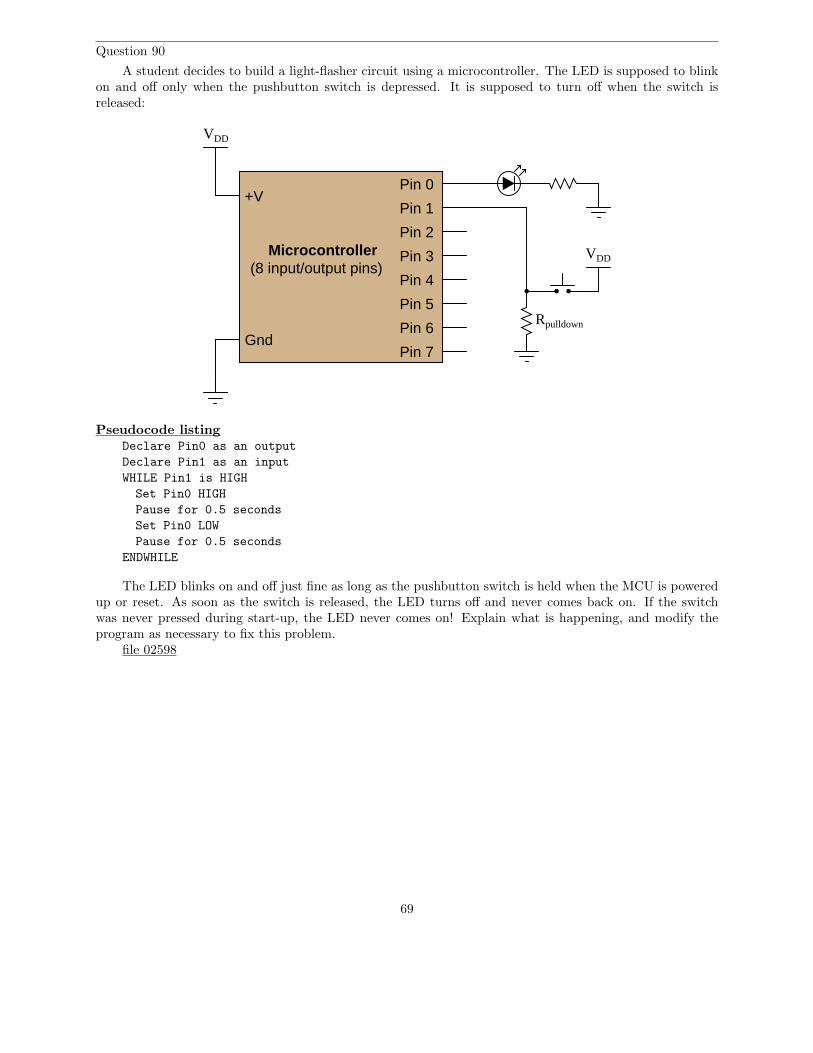
Question 90
A student decides to build a light-flasher circuit using a microcontroller. The LED is supposed to blinkon and off only when the pushbutton switch is depressed. It is supposed to turn off when the switch isreleased:
Microcontroller
+V
Gnd
(8 input/output pins)
Pin 0
Pin 1
Pin 2
Pin 3
Pin 4
Pin 5
Pin 6
Pin 7
VDD
VDD
Rpulldown
Pseudocode listingDeclare Pin0 as an output
Declare Pin1 as an input
WHILE Pin1 is HIGH
Set Pin0 HIGH
Pause for 0.5 seconds
Set Pin0 LOW
Pause for 0.5 seconds
ENDWHILE
The LED blinks on and off just fine as long as the pushbutton switch is held when the MCU is poweredup or reset. As soon as the switch is released, the LED turns off and never comes back on. If the switchwas never pressed during start-up, the LED never comes on! Explain what is happening, and modify theprogram as necessary to fix this problem.
file 02598
69

Question 91
Examine the following schematic diagram and program listing (written in ”pseudocode” rather than aformal programming language) to determine what type of basic logic function is being implemented in thismicrocontroller unit:
Microcontroller
+V
Gnd
(8 input/output pins)
Pin 0
Pin 1
Pin 2
Pin 3
Pin 4
Pin 5
Pin 6
Pin 7
VDD
VDD
Pseudocode listingDeclare Pin0 as an output
Declare Pin1 and Pin2 as inputs
LOOP
IF Pin1 is HIGH, set Pin0 HIGH
ELSEIF Pin2 is HIGH, set Pin0 HIGH
ELSE set Pin0 LOW
ENDIF
ENDLOOP
file 02582
70

Question 92
Examine the following schematic diagram and program listing (written in ”pseudocode” rather than aformal programming language) to determine what type of basic logic function is being implemented in thismicrocontroller unit:
Microcontroller
+V
Gnd
(8 input/output pins)
Pin 0
Pin 1
Pin 2
Pin 3
Pin 4
Pin 5
Pin 6
Pin 7
VDD
VDD
Pseudocode listingDeclare Pin0 as an output
Declare Pin1 and Pin2 as inputs
LOOP
IF Pin1 is LOW, set Pin0 LOW
ELSEIF Pin2 is LOW, set Pin0 LOW
ELSE set Pin0 HIGH
ENDIF
ENDLOOP
file 02583
71
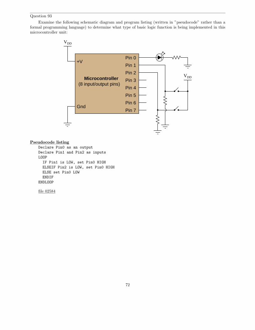
Question 93
Examine the following schematic diagram and program listing (written in ”pseudocode” rather than aformal programming language) to determine what type of basic logic function is being implemented in thismicrocontroller unit:
Microcontroller
+V
Gnd
(8 input/output pins)
Pin 0
Pin 1
Pin 2
Pin 3
Pin 4
Pin 5
Pin 6
Pin 7
VDD
VDD
Pseudocode listingDeclare Pin0 as an output
Declare Pin1 and Pin2 as inputs
LOOP
IF Pin1 is LOW, set Pin0 HIGH
ELSEIF Pin2 is LOW, set Pin0 HIGH
ELSE set Pin0 LOW
ENDIF
ENDLOOP
file 02584
72

Question 94
Examine the following schematic diagram and program listing (written in ”pseudocode” rather than aformal programming language) to determine what type of basic logic function is being implemented in thismicrocontroller unit:
Microcontroller
+V
Gnd
(8 input/output pins)
Pin 0
Pin 1
Pin 2
Pin 3
Pin 4
Pin 5
Pin 6
Pin 7
VDD
VDD
Pseudocode listingDeclare Pin0 as an output
Declare Pin1 and Pin2 as inputs
LOOP
IF Pin1 is HIGH, set Pin0 LOW
ELSEIF Pin2 is HIGH, set Pin0 LOW
ELSE set Pin0 HIGH
ENDIF
ENDLOOP
file 02585
73
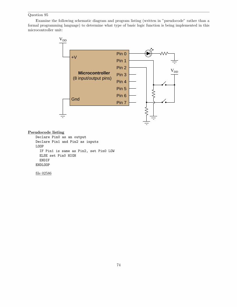
Question 95
Examine the following schematic diagram and program listing (written in ”pseudocode” rather than aformal programming language) to determine what type of basic logic function is being implemented in thismicrocontroller unit:
Microcontroller
+V
Gnd
(8 input/output pins)
Pin 0
Pin 1
Pin 2
Pin 3
Pin 4
Pin 5
Pin 6
Pin 7
VDD
VDD
Pseudocode listingDeclare Pin0 as an output
Declare Pin1 and Pin2 as inputs
LOOP
IF Pin1 is same as Pin2, set Pin0 LOW
ELSE set Pin0 HIGH
ENDIF
ENDLOOP
file 02586
74
Question 96
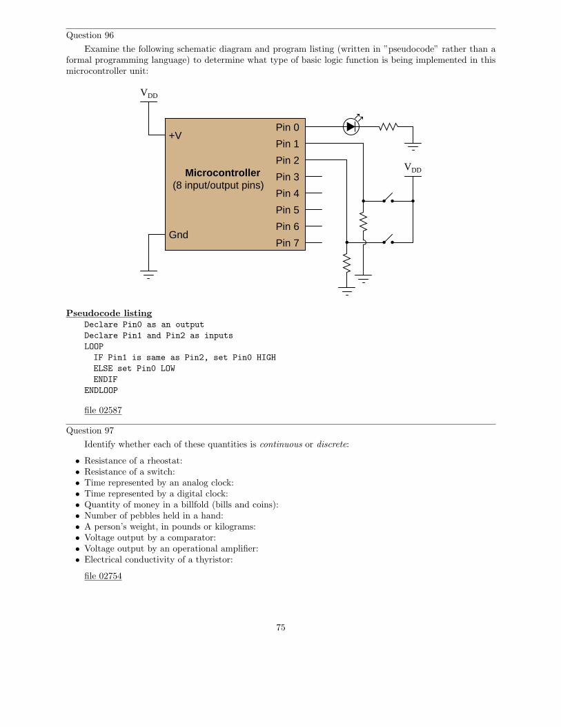
Examine the following schematic diagram and program listing (written in ”pseudocode” rather than aformal programming language) to determine what type of basic logic function is being implemented in thismicrocontroller unit:
Microcontroller
+V
Gnd
(8 input/output pins)
Pin 0
Pin 1
Pin 2
Pin 3
Pin 4
Pin 5
Pin 6
Pin 7
VDD
VDD
Pseudocode listingDeclare Pin0 as an output
Declare Pin1 and Pin2 as inputs
LOOP
IF Pin1 is same as Pin2, set Pin0 HIGH
ELSE set Pin0 LOW
ENDIF
ENDLOOP
file 02587
Question 97
Identify whether each of these quantities is continuous or discrete:
• Resistance of a rheostat:• Resistance of a switch:• Time represented by an analog clock:• Time represented by a digital clock:• Quantity of money in a billfold (bills and coins):• Number of pebbles held in a hand:• A person’s weight, in pounds or kilograms:• Voltage output by a comparator:• Voltage output by an operational amplifier:• Electrical conductivity of a thyristor:
file 02754
75
Question 98
Two computational aids of antiquity are the abacus and the slide rule. Which of these mathematicalinstruments would be considered ”analog” and which would be considered ”digital”? Explain your answer.
file 02757
Question 99
In digital electronic circuitry, binary bit values of 0 or 1 are represented in the form of voltages: lowand high logic states, respectively. Suppose you need to manually ”input” a logic state to one of the pinsof a logic circuit. In the following illustration, the logic circuit (shown as an indistinct, shaded rectangle) isalready supplied with DC power (+V and ground), and its output is indicated by an LED. All it requires isan input from you:
+V
Logic circuitInput Output
Complete this schematic diagram by including a switch in the drawing, such that in each of its twopositions, a definite ”low” or ”high” logic state will be sensed by the circuit’s input terminal.
file 01251
Question 100
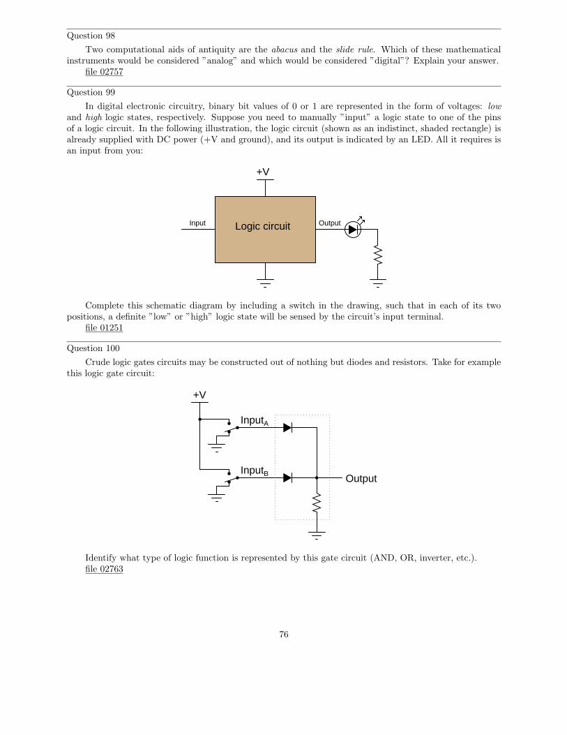
Crude logic gates circuits may be constructed out of nothing but diodes and resistors. Take for examplethis logic gate circuit:
+V
Output
InputA
InputB
Identify what type of logic function is represented by this gate circuit (AND, OR, inverter, etc.).file 02763
76
Question 101
One way to think of the basic logic gate types (all but the XOR and XNOR gates) is to consider whatsingle input state guarantees a certain output state. For example, we could describe the function of an ORgate as such:
Any high input guarantees a high output.
Identify what type of gate is represented by each of the following phrases:
• Any high input guarantees a low output.• Any low input guarantees a high output.• Any low input guarantees a low output.
file 02891
Question 102
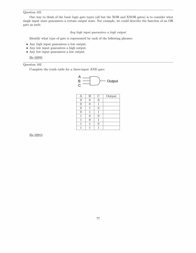
Complete the truth table for a three-input AND gate:
ABC
Output
A B C Output0 0 00 0 10 1 00 1 11 0 01 0 11 1 01 1 1
file 02915
77
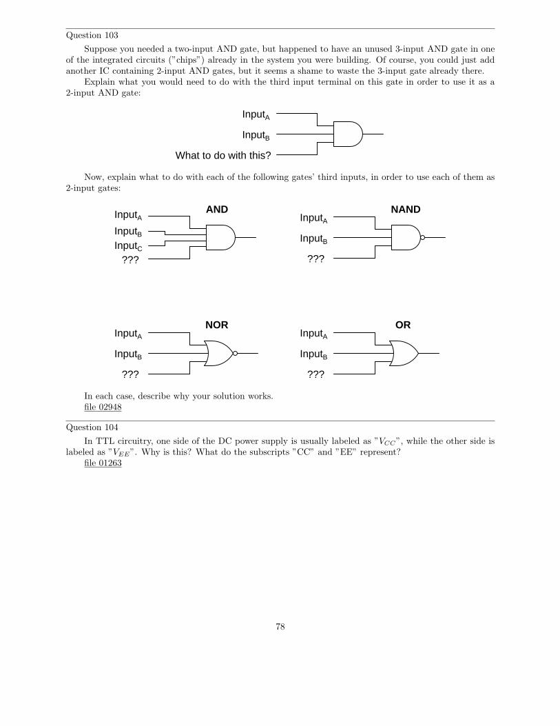
Question 103
Suppose you needed a two-input AND gate, but happened to have an unused 3-input AND gate in oneof the integrated circuits (”chips”) already in the system you were building. Of course, you could just addanother IC containing 2-input AND gates, but it seems a shame to waste the 3-input gate already there.
Explain what you would need to do with the third input terminal on this gate in order to use it as a2-input AND gate:
InputA
InputB
What to do with this?
Now, explain what to do with each of the following gates’ third inputs, in order to use each of them as2-input gates:
InputA
???
InputB
InputA
???
InputB
InputA
???
InputB
InputA
???
InputB
InputC
AND NAND
NOR OR
In each case, describe why your solution works.file 02948
Question 104
In TTL circuitry, one side of the DC power supply is usually labeled as ”VCC”, while the other side islabeled as ”VEE”. Why is this? What do the subscripts ”CC” and ”EE” represent?
file 01263
78
Question 105
True story: once upon a time, there was a machine shop containing a number of computer-controlledmachine tools (lathes, mills, grinders, etc.), where one of the machines proved to be very ”finicky” whenstarting. Sometimes, it would function properly when you pushed the ”Start” button, and other timesit refused to work at all. The problem was so bad, it got to the point where the machinists responsiblefor operating this tool became almost superstitious about it, performing a ritual dance before pressing the”Start” button, whimsically hoping to improve their luck.
An electrician was called to service this machine, but he could find nothing wrong with the electricalpower circuitry. All of the high-voltage equipment (transformers, relays, motors, motor control circuits, etc.)seemed to be in good working order. The problem, whatever it was, resided within the machine’s electroniccontrol computer. The computer was not sending the ”start” signal to the motor control circuits when the”Start” button was pushed.
An electronics technician was called to troubleshoot the computer, and he was able to fix it in a matterof minutes. The problem, he said, was the computer’s DC power supply: the voltage regulator was out ofadjustment. With just a twist of a potentiometer, the technician was able to ”trim” the regulated voltageto 5.00 volts, right where it should be for TTL circuitry.
The power supply voltage was not very far from 5.00 volts before the technician adjusted it. How faris the supply voltage allowed to deviate for TTL logic circuits, and still have guaranteed proper operation?Consult one or more IC datasheets for legacy TTL logic circuits (not the newer high-speed CMOS 54HCxxand 74HCxx chips) to obtain your answer.
file 01261
79
Question 106
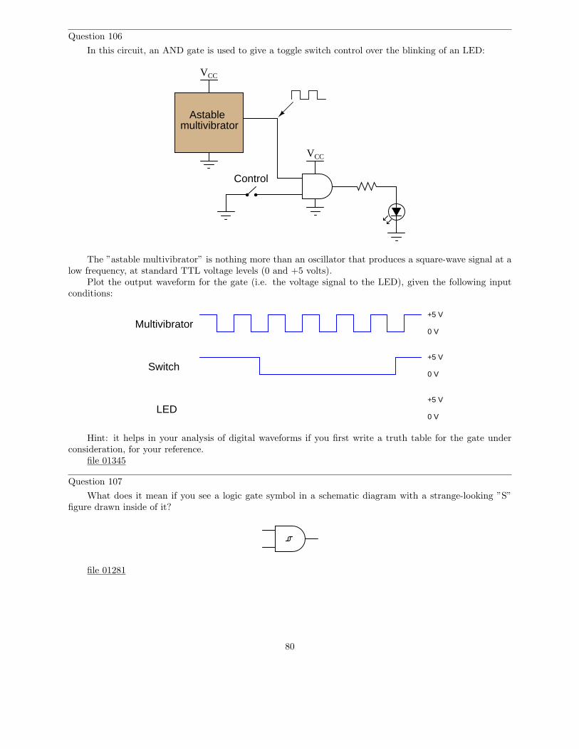
In this circuit, an AND gate is used to give a toggle switch control over the blinking of an LED:
Astablemultivibrator
VCC
VCC
Control
The ”astable multivibrator” is nothing more than an oscillator that produces a square-wave signal at alow frequency, at standard TTL voltage levels (0 and +5 volts).
Plot the output waveform for the gate (i.e. the voltage signal to the LED), given the following inputconditions:
Multivibrator
Switch
LED
+5 V
0 V
+5 V
0 V
+5 V
0 V
Hint: it helps in your analysis of digital waveforms if you first write a truth table for the gate underconsideration, for your reference.
file 01345
Question 107
What does it mean if you see a logic gate symbol in a schematic diagram with a strange-looking ”S”figure drawn inside of it?
file 01281
80
Question 108
In CMOS circuitry, one side of the DC power supply is usually labeled as ”VDD”, while the other sideis labeled as ”VSS”. Why is this? What do the subscripts ”DD” and ”SS” represent?
file 01273
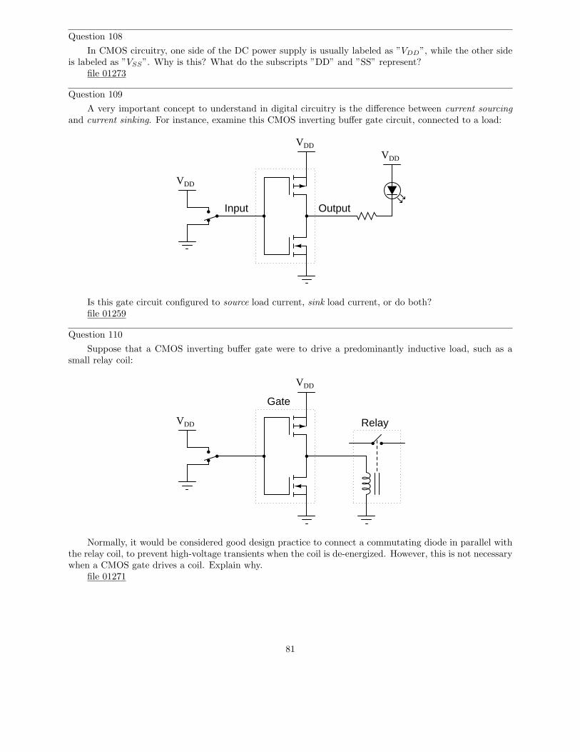
Question 109
A very important concept to understand in digital circuitry is the difference between current sourcingand current sinking. For instance, examine this CMOS inverting buffer gate circuit, connected to a load:
VDD
Input
VDD
Output
VDD
Is this gate circuit configured to source load current, sink load current, or do both?file 01259
Question 110
Suppose that a CMOS inverting buffer gate were to drive a predominantly inductive load, such as asmall relay coil:
VDD
VDD Relay
Gate
Normally, it would be considered good design practice to connect a commutating diode in parallel withthe relay coil, to prevent high-voltage transients when the coil is de-energized. However, this is not necessarywhen a CMOS gate drives a coil. Explain why.
file 01271
81

Question 111
A problem unique to certain types of CMOS logic gates is something called SCR latchup. This is anabnormal condition capable of ruining a circuit, or at the very least causing operational problems in a circuit.Explain what this phenomenon is, and what causes it.
file 01248
Question 112
Explain why placing static-sensitive components (such as CMOS integrated circuits) into a block ofconductive foam protects them against damage from ESD, and why this protection exists even if the entireblock of foam (with chip) is brought to an elevated potential with respect to earth ground.
file 02869
82
Question 113
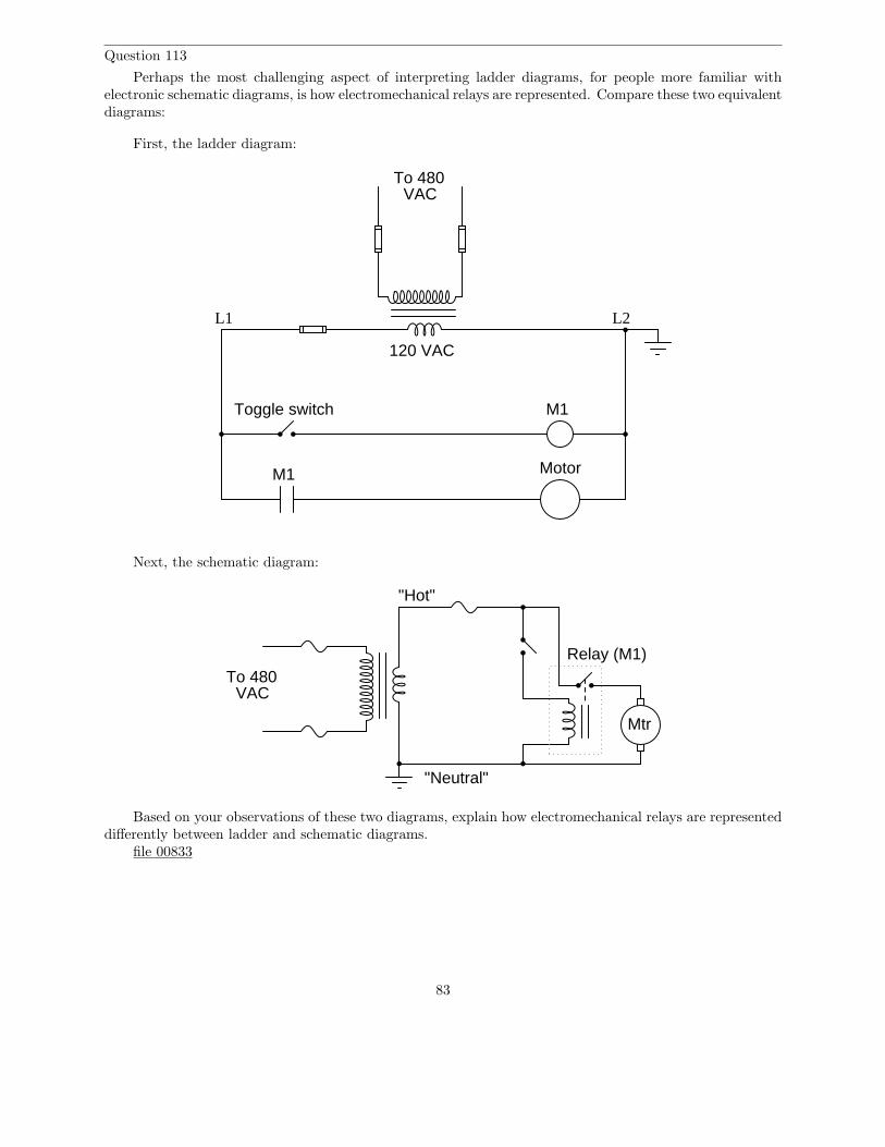
Perhaps the most challenging aspect of interpreting ladder diagrams, for people more familiar withelectronic schematic diagrams, is how electromechanical relays are represented. Compare these two equivalentdiagrams:
First, the ladder diagram:
To 480VAC
120 VAC
Toggle switch M1
M1 Motor
L1 L2
Next, the schematic diagram:
To 480VAC
"Hot"
"Neutral"
Mtr
Relay (M1)
Based on your observations of these two diagrams, explain how electromechanical relays are representeddifferently between ladder and schematic diagrams.
file 00833
83
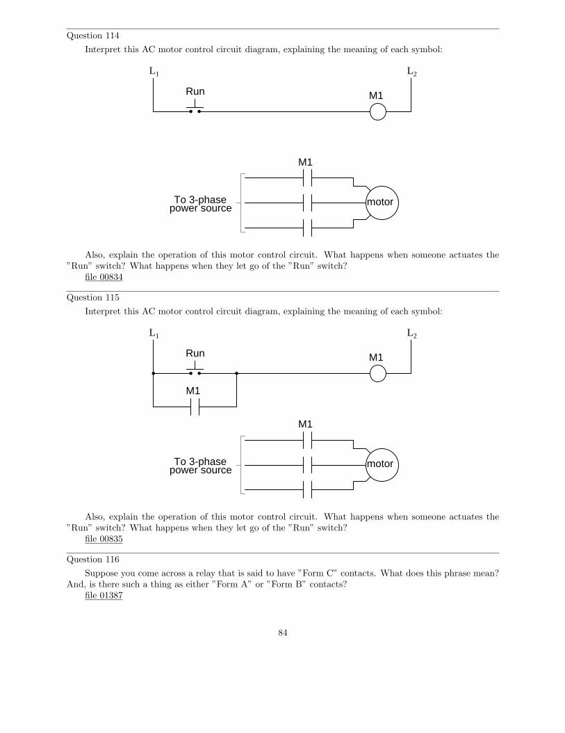
Question 114
Interpret this AC motor control circuit diagram, explaining the meaning of each symbol:
L1 L2
M1Run
motorTo 3-phasepower source
M1
Also, explain the operation of this motor control circuit. What happens when someone actuates the”Run” switch? What happens when they let go of the ”Run” switch?
file 00834
Question 115
Interpret this AC motor control circuit diagram, explaining the meaning of each symbol:
L1 L2
M1Run
motorTo 3-phasepower source
M1
M1
Also, explain the operation of this motor control circuit. What happens when someone actuates the”Run” switch? What happens when they let go of the ”Run” switch?
file 00835
Question 116
Suppose you come across a relay that is said to have ”Form C” contacts. What does this phrase mean?And, is there such a thing as either ”Form A” or ”Form B” contacts?
file 01387
84
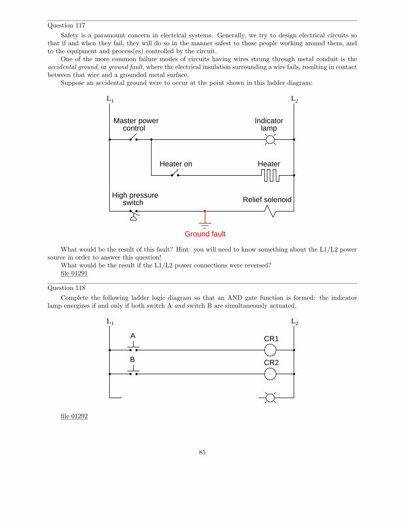
Question 117
Safety is a paramount concern in electrical systems. Generally, we try to design electrical circuits sothat if and when they fail, they will do so in the manner safest to those people working around them, andto the equipment and process(es) controlled by the circuit.
One of the more common failure modes of circuits having wires strung through metal conduit is theaccidental ground, or ground fault, where the electrical insulation surrounding a wire fails, resulting in contactbetween that wire and a grounded metal surface.
Suppose an accidental ground were to occur at the point shown in this ladder diagram:
L1 L2
Indicatorlamp
HeaterHeater on
Master powercontrol
High pressureswitch Relief solenoid
Ground fault
What would be the result of this fault? Hint: you will need to know something about the L1/L2 powersource in order to answer this question!
What would be the result if the L1/L2 power connections were reversed?file 01291
Question 118
Complete the following ladder logic diagram so that an AND gate function is formed: the indicatorlamp energizes if and only if both switch A and switch B are simultaneously actuated.
L1 L2
CR1A
B CR2
file 01292
85
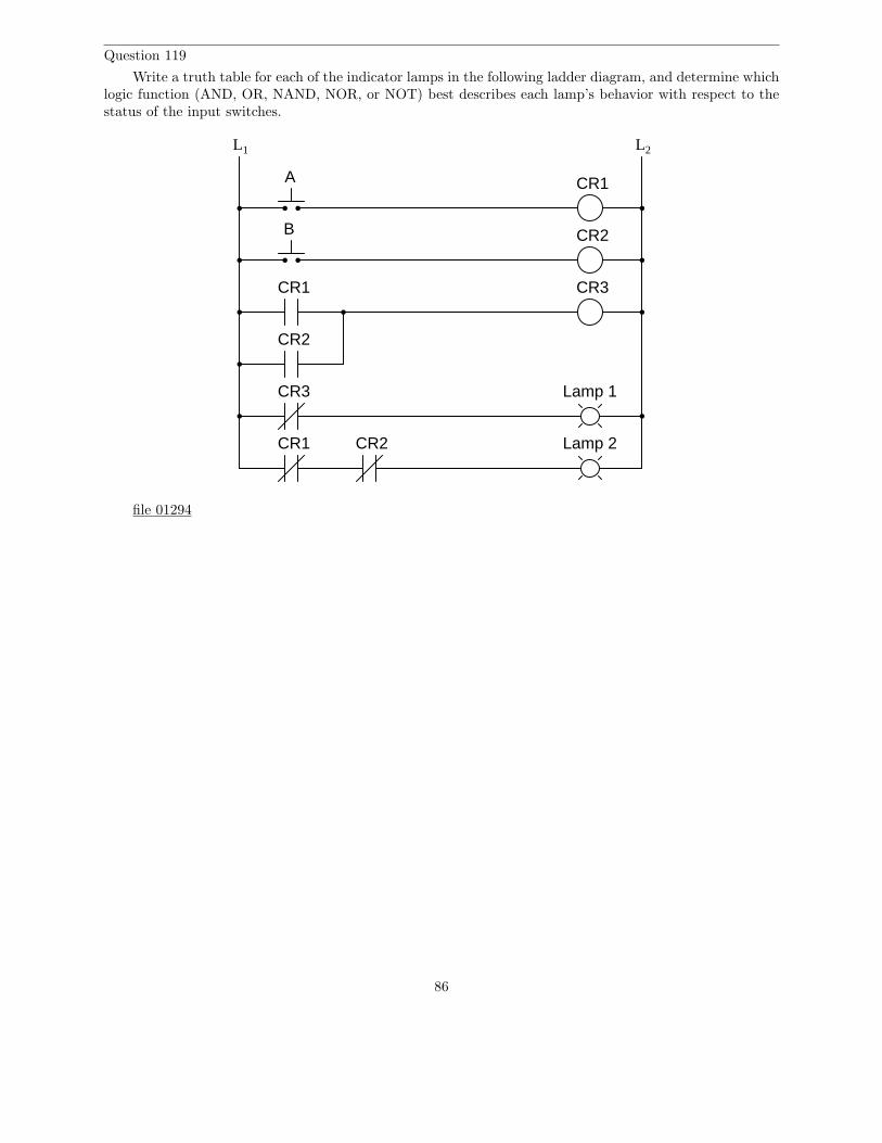
Question 119
Write a truth table for each of the indicator lamps in the following ladder diagram, and determine whichlogic function (AND, OR, NAND, NOR, or NOT) best describes each lamp’s behavior with respect to thestatus of the input switches.
L1 L2
CR1A
B CR2
CR1
CR2
CR3
CR3
CR1 CR2
Lamp 1
Lamp 2
file 01294
86
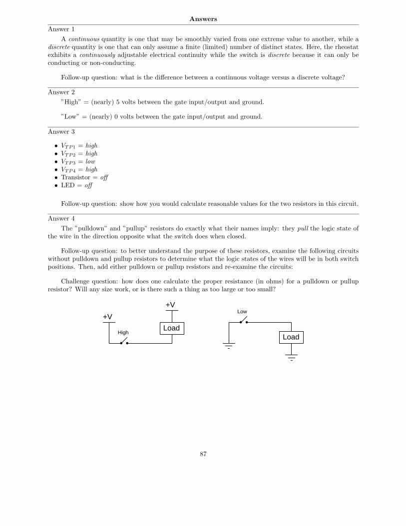
Answers
Answer 1
A continuous quantity is one that may be smoothly varied from one extreme value to another, while adiscrete quantity is one that can only assume a finite (limited) number of distinct states. Here, the rheostatexhibits a continuously adjustable electrical continuity while the switch is discrete because it can only beconducting or non-conducting.
Follow-up question: what is the difference between a continuous voltage versus a discrete voltage?
Answer 2
”High” = (nearly) 5 volts between the gate input/output and ground.
”Low” = (nearly) 0 volts between the gate input/output and ground.
Answer 3
• VTP1 = high• VTP2 = high• VTP3 = low• VTP4 = high• Transistor = off• LED = off
Follow-up question: show how you would calculate reasonable values for the two resistors in this circuit.
Answer 4
The ”pulldown” and ”pullup” resistors do exactly what their names imply: they pull the logic state ofthe wire in the direction opposite what the switch does when closed.
Follow-up question: to better understand the purpose of these resistors, examine the following circuitswithout pulldown and pullup resistors to determine what the logic states of the wires will be in both switchpositions. Then, add either pulldown or pullup resistors and re-examine the circuits:
Challenge question: how does one calculate the proper resistance (in ohms) for a pulldown or pullupresistor? Will any size work, or is there such a thing as too large or too small?
+V
High
Low
Load
+V
Load
87
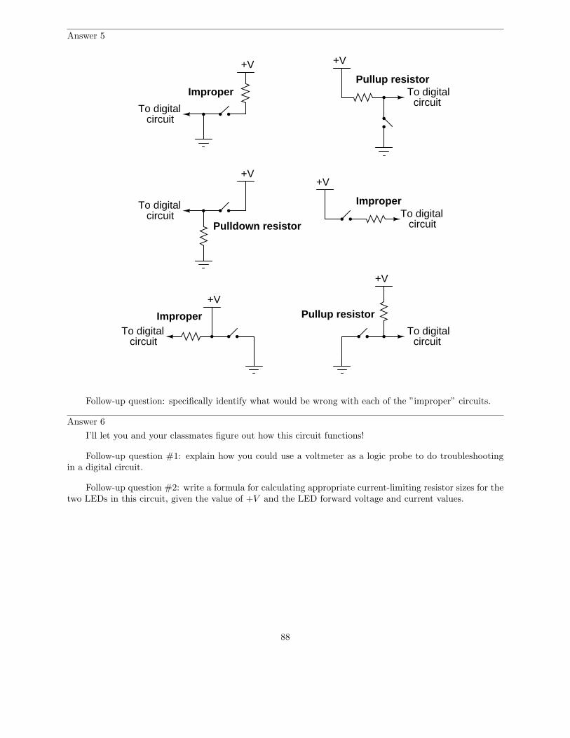
Answer 5
+V
+V
To digitalcircuit
circuitTo digital
+V
circuitTo digital
+V
circuitTo digital
+V
To digitalcircuit
+V
circuitTo digital
ImproperPullup resistor
Pulldown resistor
Improper
Improper Pullup resistor
Follow-up question: specifically identify what would be wrong with each of the ”improper” circuits.
Answer 6
I’ll let you and your classmates figure out how this circuit functions!
Follow-up question #1: explain how you could use a voltmeter as a logic probe to do troubleshootingin a digital circuit.
Follow-up question #2: write a formula for calculating appropriate current-limiting resistor sizes for thetwo LEDs in this circuit, given the value of +V and the LED forward voltage and current values.
88
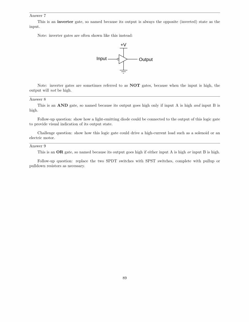
Answer 7
This is an inverter gate, so named because its output is always the opposite (inverted) state as theinput.
Note: inverter gates are often shown like this instead:
+V
OutputInput
Note: inverter gates are sometimes referred to as NOT gates, because when the input is high, theoutput will not be high.
Answer 8
This is an AND gate, so named because its output goes high only if input A is high and input B ishigh.
Follow-up question: show how a light-emitting diode could be connected to the output of this logic gateto provide visual indication of its output state.
Challenge question: show how this logic gate could drive a high-current load such as a solenoid or anelectric motor.
Answer 9
This is an OR gate, so named because its output goes high if either input A is high or input B is high.
Follow-up question: replace the two SPDT switches with SPST switches, complete with pullup orpulldown resistors as necessary.
89
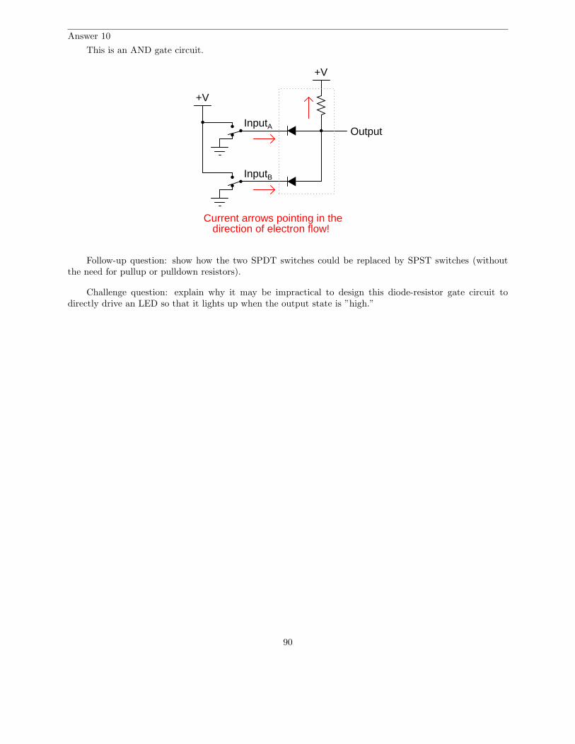
Answer 10
This is an AND gate circuit.
+V
+V
OutputInputA
InputB
direction of electron flow!Current arrows pointing in the
Follow-up question: show how the two SPDT switches could be replaced by SPST switches (withoutthe need for pullup or pulldown resistors).
Challenge question: explain why it may be impractical to design this diode-resistor gate circuit todirectly drive an LED so that it lights up when the output state is ”high.”
90
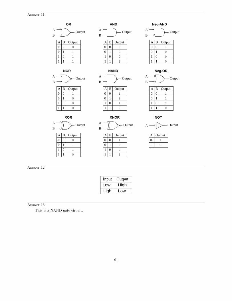
Answer 11
A B Output
00
0 1
01
1 1
A
BOutput
A B Output
00
0 1
01
1 1
A
BOutput
A B Output
00
0 1
01
1 1
A
BOutput
A B Output
00
0 1
01
1 1
A
BOutput
A B Output
00
0 1
01
1 1
A
BOutput
A B Output
00
0 1
01
1 1
A
BOutput
A B Output
00
0 1
01
1 1
A
BOutput
A B Output
00
0 1
01
1 1
A
BOutput A Output
A Output
OR AND Neg-AND
NOR NAND Neg-OR
XOR XNOR NOT
0
1
1
1
0
0
0
1
0
0
0
1 1
1
1
0
0
0
0
1
1
1
1
0
1
1
0
0
0
0
1
1
1
0
0
1
Answer 12
Input Output
Low HighHigh Low
Answer 13
This is a NAND gate circuit.
91
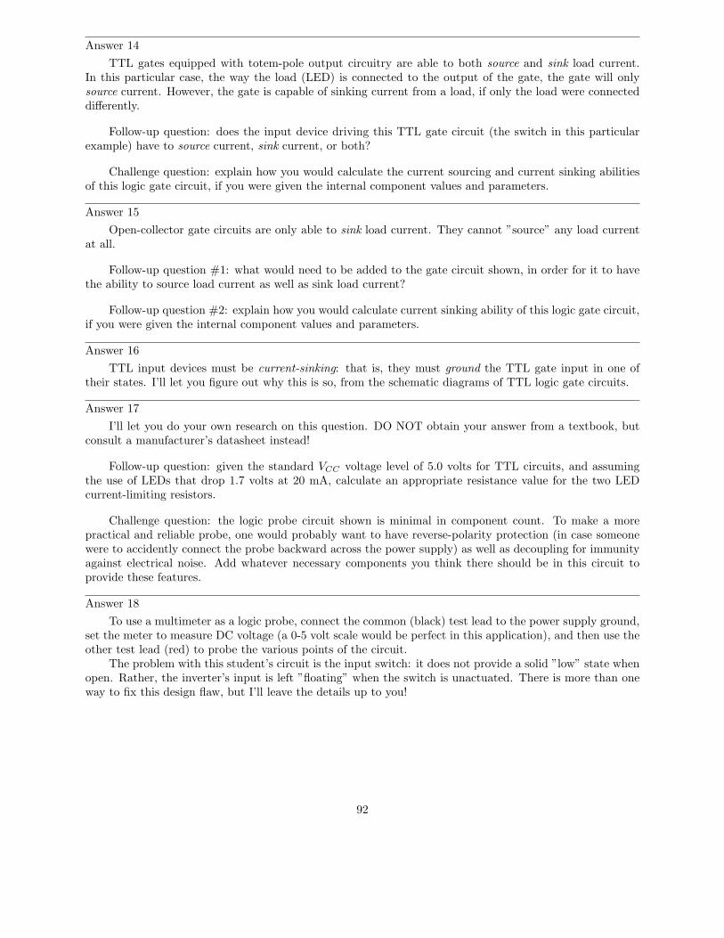
Answer 14
TTL gates equipped with totem-pole output circuitry are able to both source and sink load current.In this particular case, the way the load (LED) is connected to the output of the gate, the gate will onlysource current. However, the gate is capable of sinking current from a load, if only the load were connecteddifferently.
Follow-up question: does the input device driving this TTL gate circuit (the switch in this particularexample) have to source current, sink current, or both?
Challenge question: explain how you would calculate the current sourcing and current sinking abilitiesof this logic gate circuit, if you were given the internal component values and parameters.
Answer 15
Open-collector gate circuits are only able to sink load current. They cannot ”source” any load currentat all.
Follow-up question #1: what would need to be added to the gate circuit shown, in order for it to havethe ability to source load current as well as sink load current?
Follow-up question #2: explain how you would calculate current sinking ability of this logic gate circuit,if you were given the internal component values and parameters.
Answer 16
TTL input devices must be current-sinking: that is, they must ground the TTL gate input in one oftheir states. I’ll let you figure out why this is so, from the schematic diagrams of TTL logic gate circuits.
Answer 17
I’ll let you do your own research on this question. DO NOT obtain your answer from a textbook, butconsult a manufacturer’s datasheet instead!
Follow-up question: given the standard VCC voltage level of 5.0 volts for TTL circuits, and assumingthe use of LEDs that drop 1.7 volts at 20 mA, calculate an appropriate resistance value for the two LEDcurrent-limiting resistors.
Challenge question: the logic probe circuit shown is minimal in component count. To make a morepractical and reliable probe, one would probably want to have reverse-polarity protection (in case someonewere to accidently connect the probe backward across the power supply) as well as decoupling for immunityagainst electrical noise. Add whatever necessary components you think there should be in this circuit toprovide these features.
Answer 18
To use a multimeter as a logic probe, connect the common (black) test lead to the power supply ground,set the meter to measure DC voltage (a 0-5 volt scale would be perfect in this application), and then use theother test lead (red) to probe the various points of the circuit.
The problem with this student’s circuit is the input switch: it does not provide a solid ”low” state whenopen. Rather, the inverter’s input is left ”floating” when the switch is unactuated. There is more than oneway to fix this design flaw, but I’ll leave the details up to you!
92
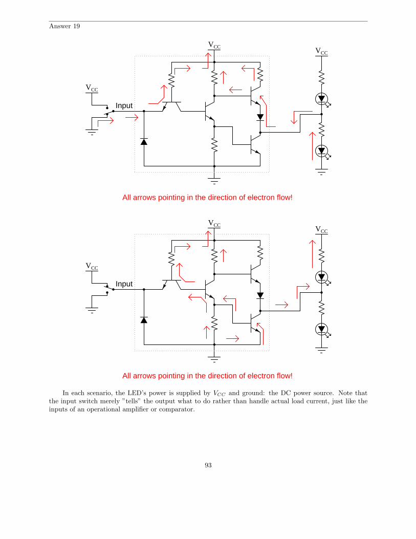
Answer 19
VCC
Input
VCC
VCC
All arrows pointing in the direction of electron flow!
VCC
Input
VCC
VCC
All arrows pointing in the direction of electron flow!
In each scenario, the LED’s power is supplied by VCC and ground: the DC power source. Note thatthe input switch merely ”tells” the output what to do rather than handle actual load current, just like theinputs of an operational amplifier or comparator.
93
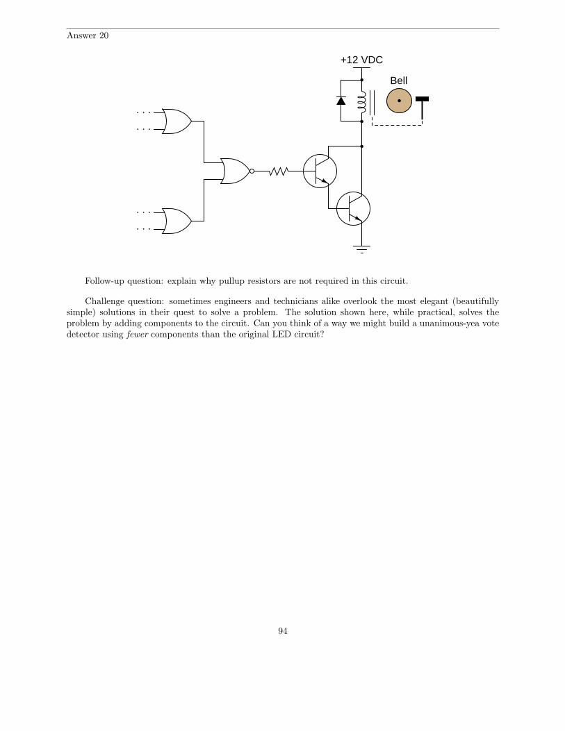
Answer 20
. . .
. . .
. . .
. . .
+12 VDC
Bell
Follow-up question: explain why pullup resistors are not required in this circuit.
Challenge question: sometimes engineers and technicians alike overlook the most elegant (beautifullysimple) solutions in their quest to solve a problem. The solution shown here, while practical, solves theproblem by adding components to the circuit. Can you think of a way we might build a unanimous-yea votedetector using fewer components than the original LED circuit?
94
Answer 21
A B Output
00
0 1
01
1 1
A
BOutput
A B Output
00
0 1
01
1 1
A
BOutput
A B Output
00
0 1
01
1 1
A
BOutput
A B Output
00
0 1
01
1 1
A
BOutput
A B Output
00
0 1
01
1 1
A
BOutput
A B Output
00
0 1
01
1 1
A
BOutput
A B Output
00
0 1
01
1 1
A
BOutput
A B Output
00
0 1
01
1 1
A
BOutput
A Output
A Output
OR
AND
Neg-ANDNOR
NAND
Neg-ORXOR
XNOR
NOT
0
1
1
1
0
0
0
1
0
0
0
1
1
1
1
0
0
0
0
1
1
1
1
0
1
1
0
0
0
0
1
1
1
0
0
1
Answer 22
Input Output
Low HighHigh Low
Answer 23
Two of the diodes protect against input voltages exceeding the supply rails, while the third diode protectsagainst a reverse-connected power supply.
Answer 24
The resistor on the input side of the gate functions as a pulldown, to provide a solid ”low” state to thegate’s input when the switch contacts open.
Shorting all unused gate inputs to either ground or VDD is merely a precautionary measure. It preventsunnecessary power draw from the supply, and possible IC overheating.
95
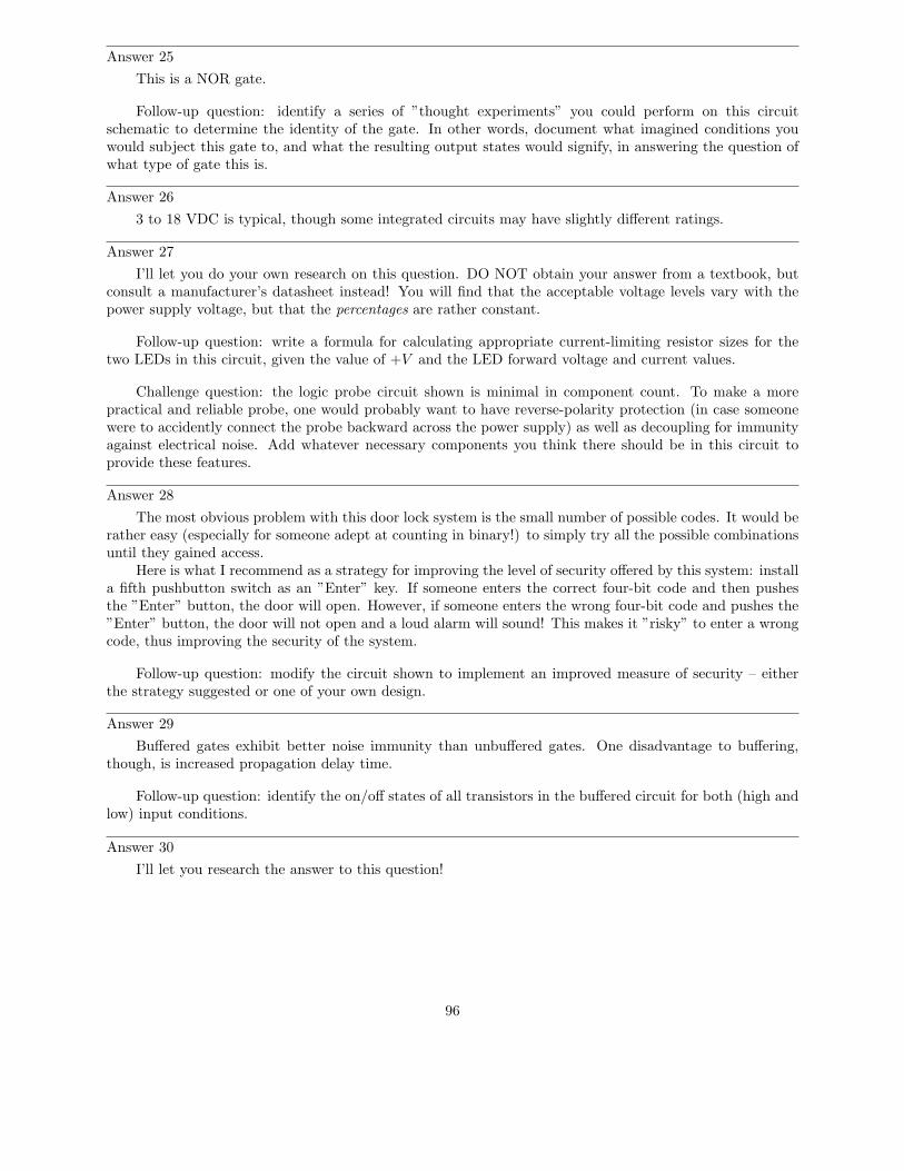
Answer 25
This is a NOR gate.
Follow-up question: identify a series of ”thought experiments” you could perform on this circuitschematic to determine the identity of the gate. In other words, document what imagined conditions youwould subject this gate to, and what the resulting output states would signify, in answering the question ofwhat type of gate this is.
Answer 26
3 to 18 VDC is typical, though some integrated circuits may have slightly different ratings.
Answer 27
I’ll let you do your own research on this question. DO NOT obtain your answer from a textbook, butconsult a manufacturer’s datasheet instead! You will find that the acceptable voltage levels vary with thepower supply voltage, but that the percentages are rather constant.
Follow-up question: write a formula for calculating appropriate current-limiting resistor sizes for thetwo LEDs in this circuit, given the value of +V and the LED forward voltage and current values.
Challenge question: the logic probe circuit shown is minimal in component count. To make a morepractical and reliable probe, one would probably want to have reverse-polarity protection (in case someonewere to accidently connect the probe backward across the power supply) as well as decoupling for immunityagainst electrical noise. Add whatever necessary components you think there should be in this circuit toprovide these features.
Answer 28
The most obvious problem with this door lock system is the small number of possible codes. It would berather easy (especially for someone adept at counting in binary!) to simply try all the possible combinationsuntil they gained access.
Here is what I recommend as a strategy for improving the level of security offered by this system: installa fifth pushbutton switch as an ”Enter” key. If someone enters the correct four-bit code and then pushesthe ”Enter” button, the door will open. However, if someone enters the wrong four-bit code and pushes the”Enter” button, the door will not open and a loud alarm will sound! This makes it ”risky” to enter a wrongcode, thus improving the security of the system.
Follow-up question: modify the circuit shown to implement an improved measure of security – eitherthe strategy suggested or one of your own design.
Answer 29
Buffered gates exhibit better noise immunity than unbuffered gates. One disadvantage to buffering,though, is increased propagation delay time.
Follow-up question: identify the on/off states of all transistors in the buffered circuit for both (high andlow) input conditions.
Answer 30
I’ll let you research the answer to this question!
96
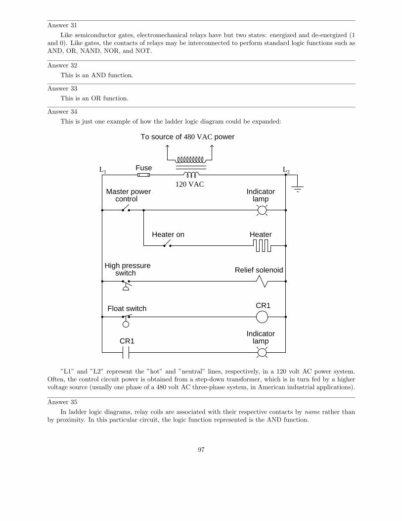
Answer 31
Like semiconductor gates, electromechanical relays have but two states: energized and de-energized (1and 0). Like gates, the contacts of relays may be interconnected to perform standard logic functions such asAND, OR, NAND, NOR, and NOT.
Answer 32
This is an AND function.
Answer 33
This is an OR function.
Answer 34
This is just one example of how the ladder logic diagram could be expanded:
L1 L2
Indicatorlamp
HeaterHeater on
Master powercontrol
High pressureswitch Relief solenoid
Fuse
120 VAC
To source of 480 VAC power
CR1
CR1Indicator
lamp
Float switch
”L1” and ”L2” represent the ”hot” and ”neutral” lines, respectively, in a 120 volt AC power system.Often, the control circuit power is obtained from a step-down transformer, which is in turn fed by a highervoltage source (usually one phase of a 480 volt AC three-phase system, in American industrial applications).
Answer 35
In ladder logic diagrams, relay coils are associated with their respective contacts by name rather thanby proximity. In this particular circuit, the logic function represented is the AND function.
97
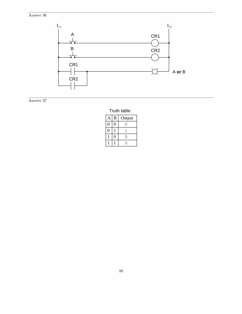
Answer 36
L1 L2
CR1A
B CR2
CR1
CR2
A or B
Answer 37
A B Output
00
0 1
01
1 1
Truth table
0
1
0
0
98
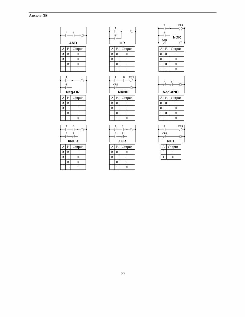
Answer 38
A B Output
00
0 1
01
1 1
A B Output
00
0 1
01
1 1
A B Output
00
0 1
01
1 1
A B Output
00
0 1
01
1 1
A B Output
00
0 1
01
1 1
A B Output
00
0 1
01
1 1
A B Output
00
0 1
01
1 1
A B Output
00
0 1
01
1 1
A Output
A
BA B
A
B
CR1
CR1
A B CR1
CR1A B
A
B
A B
A B
A B
A B
A CR1
CR1
0
1
0
0
1
1
1
0 1
0
0
0
1
0
1
1
0
1
1
1 1
0
0
0
1
0
0
0
1
1
1
1
0
0
AND OR
NOR
Neg-ANDNANDNeg-OR
XORXNOR NOT
0
1
99
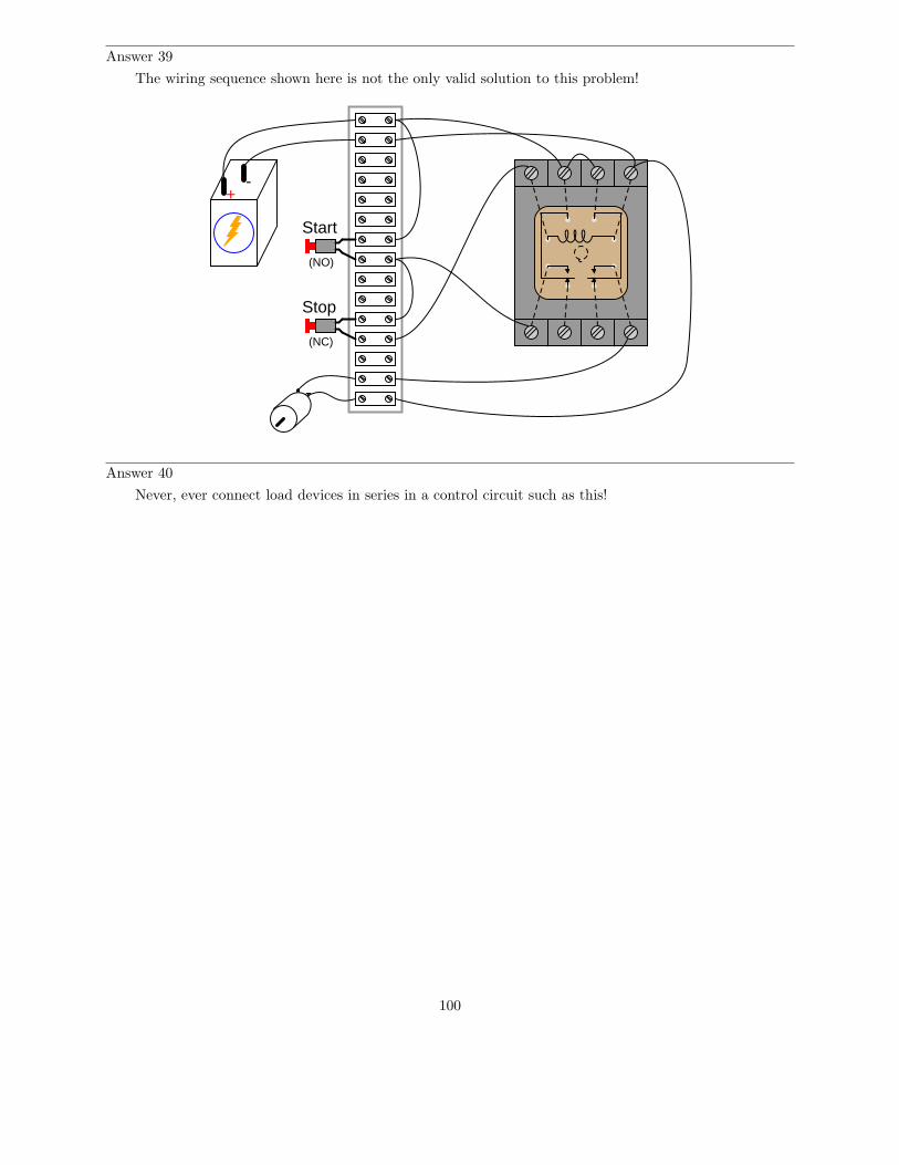
Answer 39
The wiring sequence shown here is not the only valid solution to this problem!
+-
Start
Stop
(NO)
(NC)
Answer 40
Never, ever connect load devices in series in a control circuit such as this!
100
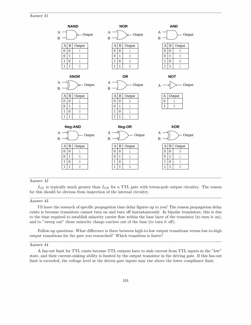
Answer 41
A B Output
00
0 1
01
1 1
A
BOutput
A B Output
00
0 1
01
1 1
A
BOutput
A B Output
00
0 1
01
1 1
A
BOutput
A B Output
00
0 1
01
1 1
A
BOutput
A B Output
00
0 1
01
1 1
A
BOutput
A B Output
00
0 1
01
1 1
A
BOutput
A B Output
00
0 1
01
1 1
A
BOutput
A B Output
00
0 1
01
1 1
A
BOutput A Output
A Output
OR
AND
Neg-AND
NORNAND
Neg-OR XOR
XNOR NOT
0
1
1
1
0
0
0
1
0
0
0
11
1
1
0
0
0
0
1 1
1
1
0
1
1
0
0
0
0
1
1
1
01
0
Answer 42
IOL is typically much greater than IOH for a TTL gate with totem-pole output circuitry. The reasonfor this should be obvious from inspection of the internal circuitry.
Answer 43
I’ll leave the research of specific propagation time delay figures up to you! The reason propagation delayexists is because transistors cannot turn on and turn off instantaneously. In bipolar transistors, this is dueto the time required to establish minority carrier flow within the base layer of the transistor (to turn it on),and to ”sweep out” those minority charge carriers out of the base (to turn it off).
Follow-up questions: What difference is there between high-to-low output transitions versus low-to-highoutput transitions for the gate you researched? Which transition is faster?
Answer 44
A fan-out limit for TTL exists because TTL outputs have to sink current from TTL inputs in the ”low”state, and their current-sinking ability is limited by the output transistor in the driving gate. If this fan-outlimit is exceeded, the voltage level at the driven gate inputs may rise above the lower compliance limit.
101

Answer 45
Logic gates will be damaged if one tries to sink the output current sourced by another.
Answer 46
Noise margin is the difference between the acceptable voltage limits for corresponding input and outputlogic states.
Answer 47
I’ll leave the research of specific propagation time delay figures up to you! The reason propagationdelay exists is because transistors cannot turn on and turn off instantaneously. In insulated-gate field-effecttransistors, this is primarily due to the time required to charge or discharge the gate-to-channel capacitance.
Follow-up questions: What difference is there between high-to-low output transitions versus low-to-highoutput transitions for the gate you researched? Which transition is faster?
Answer 48
A fan-out limit for CMOS exists because CMOS outputs have to source and sink capacitive chargingand discharging current from the CMOS inputs. I’ll let you determine why this limit is frequency-dependent.
Answer 49
Noise margin is the difference between the acceptable voltage limits for corresponding input and outputlogic states.
Answer 50
Lower operating voltages result in less power dissipation. However, noise margins become ”tighter”under the same conditions, which is a disadvantage.
Answer 51
Use circuit simulation software to verify your predicted and actual truth tables.
Answer 52
Use circuit simulation software to verify your predicted and actual truth tables.
Answer 53
Use circuit simulation software to verify your predicted and actual truth tables.
Answer 54
Use circuit simulation software to verify your predicted and actual truth tables.
Answer 55
Use circuit simulation software to verify your predicted and actual truth tables.
Answer 56
Be sure you meet with your instructor if you have any questions about what is expected for your project!
102
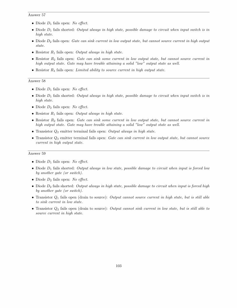
Answer 57
• Diode D1 fails open: No effect.
• Diode D1 fails shorted: Output always in high state, possible damage to circuit when input switch is inhigh state.
• Diode D2 fails open: Gate can sink current in low output state, but cannot source current in high outputstate.
• Resistor R1 fails open: Output always in high state.
• Resistor R2 fails open: Gate can sink some current in low output state, but cannot source current inhigh output state. Gate may have trouble attaining a solid ”low” output state as well.
• Resistor R4 fails open: Limited ability to source current in high output state.
Answer 58
• Diode D1 fails open: No effect.
• Diode D1 fails shorted: Output always in high state, possible damage to circuit when input switch is inhigh state.
• Diode D2 fails open: No effect.
• Resistor R1 fails open: Output always in high state.
• Resistor R2 fails open: Gate can sink some current in low output state, but cannot source current inhigh output state. Gate may have trouble attaining a solid ”low” output state as well.
• Transistor Q2 emitter terminal fails open: Output always in high state.
• Transistor Q3 emitter terminal fails open: Gate can sink current in low output state, but cannot sourcecurrent in high output state.
Answer 59
• Diode D1 fails open: No effect.
• Diode D1 fails shorted: Output always in low state, possible damage to circuit when input is forced lowby another gate (or switch).
• Diode D2 fails open: No effect.
• Diode D2 fails shorted: Output always in high state, possible damage to circuit when input is forced highby another gate (or switch).
• Transistor Q1 fails open (drain to source): Output cannot source current in high state, but is still ableto sink current in low state.
• Transistor Q2 fails open (drain to source): Output cannot sink current in low state, but is still able tosource current in high state.
103
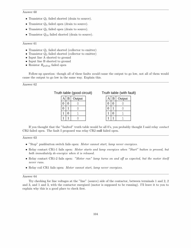
Answer 60
• Transistor Q1 failed shorted (drain to source).
• Transistor Q4 failed open (drain to source).
• Transistor Q5 failed open (drain to source).
• Transistor Q10 failed shorted (drain to source).
Answer 61
• Transistor Q1 failed shorted (collector to emitter)• Transistor Q2 failed shorted (collector to emitter)• Input line A shorted to ground• Input line B shorted to ground• Resistor Rpullup failed open
Follow-up question: though all of these faults would cause the output to go low, not all of them wouldcause the output to go low in the same way. Explain this.
Answer 62
A B Output
00
0 1
01
1 1
A B Output
00
0 1
01
1 1
Truth table (good circuit) Truth table (with fault)
1
0
0
0
1
0
0
1
If you thought that the ”faulted” truth table would be all 0’s, you probably thought I said relay contactCR2 failed open. The fault I proposed was relay CR2 coil failed open.
Answer 63
• ”Stop” pushbutton switch fails open: Motor cannot start, lamp never energizes.
• Relay contact CR1-1 fails open: Motor starts and lamp energizes when ”Start” button is pressed, butboth immediately de-energize when it is released.
• Relay contact CR1-2 fails open: ”Motor run” lamp turns on and off as expected, but the motor itselfnever runs.
• Relay coil CR1 fails open: Motor cannot start, lamp never energizes.
Answer 64
Try checking for line voltages at the ”line” (source) side of the contactor, between terminals 1 and 2, 2and 3, and 1 and 3, with the contactor energized (motor is supposed to be running). I’ll leave it to you toexplain why this is a good place to check first.
104

Answer 65
Here are some possible faults (not an exhaustive list by any means!):
• Any fuse blown• Contactor coil failed open• Any transformer winding failed open• Broken jumper between H3 and H2 on the transformer• Corroded wire connection at terminal A1 or A2• Motor winding failed shorted
Follow-up question: there will be a difference in operation between the L1 fuse blowing and either theL2 or L3 fuse blowing. Explain what this difference is, and why it might serve as a clue to what was wrong.
Answer 66
The chip’s internal input protection diodes allowed the switch inputs to supply operating power to theMOSFET transistors.
Answer 67
Switch ON:
• Points 1 and 5: Voltage!• Points 6 and 7: No voltage• Points 4 and 10: No voltage• Points 9 and 12: Voltage!• Points 6 and 12: No voltage• Points 9 and 10: No voltage• Points 4 and 7: Voltage!
Switch OFF:
• Points 1 and 5: Voltage!• Points 6 and 7: No voltage• Points 4 and 10: No voltage• Points 9 and 12: No voltage• Points 6 and 12: Voltage!• Points 9 and 10: No voltage• Points 4 and 7: Voltage!
Follow-up question: explain why there will be voltage or no voltage between each of these pairs of pointsfor the two circuit conditions (switch on and switch off).
Answer 68
Disconnect the power supply from the circuit board (only one wire need be disconnected), and then usean ohmmeter to measure continuity across the switch terminals when in the ”ON” position and when in the”OFF” position. Incidentally, this is not the only way to check the switch’s continuity, but it is the mostdirect.
105
Answer 69
Only two out of the four given statements are true:
1. Between two points that are electrically common to each other, there is guaranteed to be zero voltage.4. If voltage is measured between two points, those points must not be electrically common to each other.
For those having difficultly understanding this, test the following statements for truth. Each of thesestatements follows the same logical pattern of electrical statements given at the beginning of this question:
1. All rabbits are mammals.2. All mammals are rabbits.3. All non-rabbits are non-mammals.4. All non-mammals are non-rabbits.
Answer 70
• Slight sensation at point(s) of contact: 1.85 volts• Threshold of bodily perception: 4.3 volts• Pain, with voluntary muscle control maintained: 36.9 volts• Pain, with loss of voluntary muscle control: 64.6 volts• Severe pain and difficulty breathing: 92.3 volts• Possible heart fibrillation after three seconds: 615 volts
Answer 71
• Point ”A” dangerous to touch• Point ”B” dangerous to touch• Point ”C” dangerous to touch when motor is turned on• Point ”D” safe to touch• Point ”E” safe to touch
Answer 72
These are all interesting points to consider as a group. I’ll let you figure out possible answers to thesequestions together in class.
Answer 73
A tag informs anyone wishing to turn the disconnect device ”on” as to when it was turned off, and whoplaced the lock(s) on it. Many lockout tags have space on for a written description so that the reason forthe lockout may be explained.
Answer 74
You should check the equipment site to be sure no one is still working on it, unaware of the impendingstartup.
Answer 75
The circles with dots show the magnetic flux vectors coming at you from out of the paper. The circleswith crosses show the magnetic flux vectors going away from you into the paper. Think of these as imagesof arrows with points (dots) and fletchings (crosses).
106
Answer 76
• Meter A = 2.5 amps• Meter B = 2.5 amps• Meter C = 0 amps
Answer 77
Φ =NI
ℜ
Answer 78
B
H
Iron
Air
Follow-up question: note that the slope of both plots are approximately equal toward the far right endof the graph. Explain this effect in terms of magnetic saturation.
Answer 79
3.6 volts
107
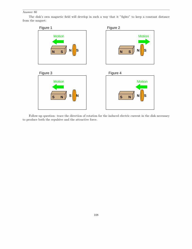
Answer 80
The disk’s own magnetic field will develop in such a way that it ”fights” to keep a constant distancefrom the magnet:
N S
Motion
N S
Motion
Figure 1 Figure 2
Figure 3 Figure 4
NS
Motion
NS
Motion
N S N S
NS N S
Follow-up question: trace the direction of rotation for the induced electric current in the disk necessaryto produce both the repulsive and the attractive force.
108
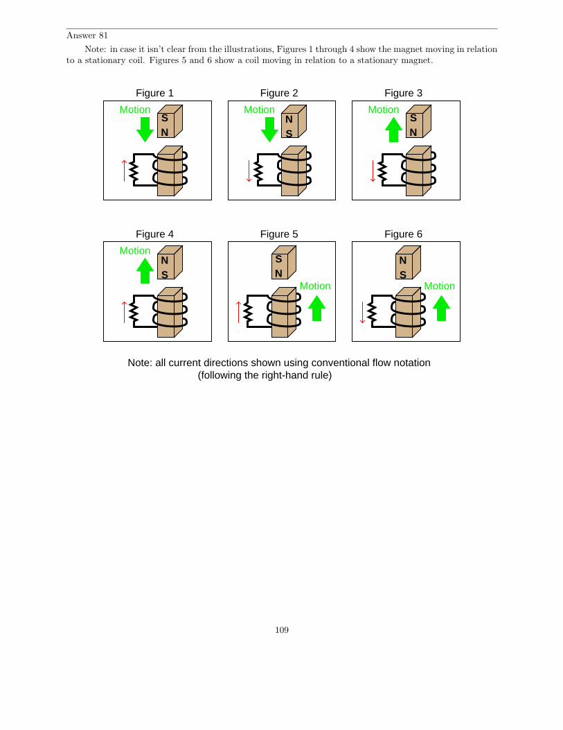
Answer 81
Note: in case it isn’t clear from the illustrations, Figures 1 through 4 show the magnet moving in relationto a stationary coil. Figures 5 and 6 show a coil moving in relation to a stationary magnet.
Figure 1 Figure 2 Figure 3
Figure 4 Figure 5 Figure 6
NS
MotionNS
Motion
NS
Motion
NS
Motion
NS
Motion
NS
Motion
Note: all current directions shown using conventional flow notation(following the right-hand rule)
109
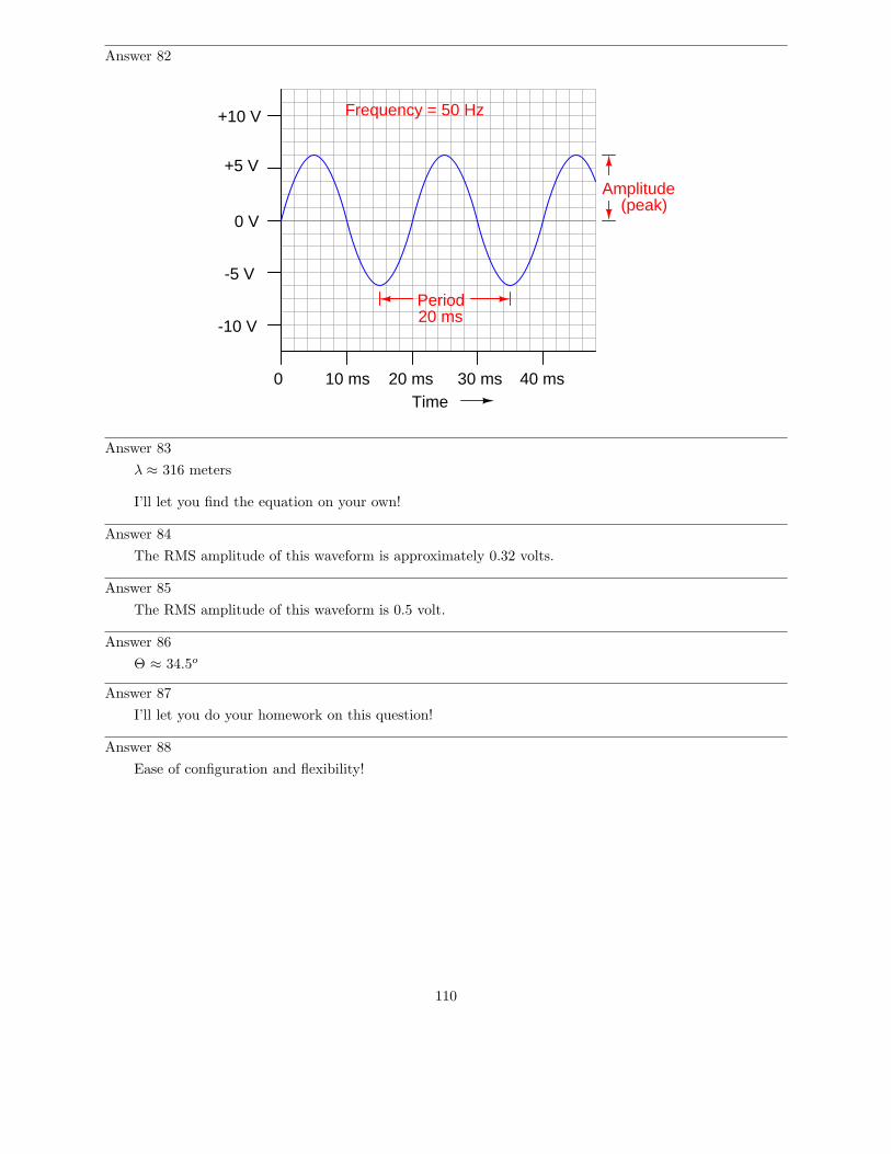
Answer 82
Time0 10 ms 20 ms 30 ms 40 ms
+5 V
+10 V
-5 V
-10 V
0 V
Amplitude(peak)
Period20 ms
Frequency = 50 Hz
Answer 83
λ ≈ 316 meters
I’ll let you find the equation on your own!
Answer 84
The RMS amplitude of this waveform is approximately 0.32 volts.
Answer 85
The RMS amplitude of this waveform is 0.5 volt.
Answer 86
Θ ≈ 34.5o
Answer 87
I’ll let you do your homework on this question!
Answer 88
Ease of configuration and flexibility!
110

Answer 89
A ”loop” is necessary for the MCU to repeat the on/pause/off sequence. What is needed now is anothertime delay within the loop:
Pseudocode listing
Declare Pin0 as an output
LOOP
Set Pin0 HIGH
Pause for 1 second
Set Pin0 LOW
Pause for 1 second (new line of code)
ENDLOOP
Answer 90
The conditional ”WHILE” loop needs to be placed inside an unconditional loop:
Pseudocode listing
Declare Pin0 as an output
Declare Pin1 as an input
LOOP
WHILE Pin1 is HIGH
Set Pin0 HIGH
Pause for 0.5 seconds
Set Pin0 LOW
Pause for 0.5 seconds
ENDWHILE
ENDLOOP
Follow-up question: what purpose does the resistor Rpulldown serve in the pushbutton circuit?
Answer 91
This microcontroller implements the logical OR function.
Answer 92
This microcontroller implements the logical AND function.
Answer 93
This microcontroller implements the logical NAND function.
Answer 94
This microcontroller implements the logical NOR function.
Answer 95
This microcontroller implements the logical Exclusive-OR function.
Answer 96
This microcontroller implements the logical Exclusive-NOR function.
Answer 97
111
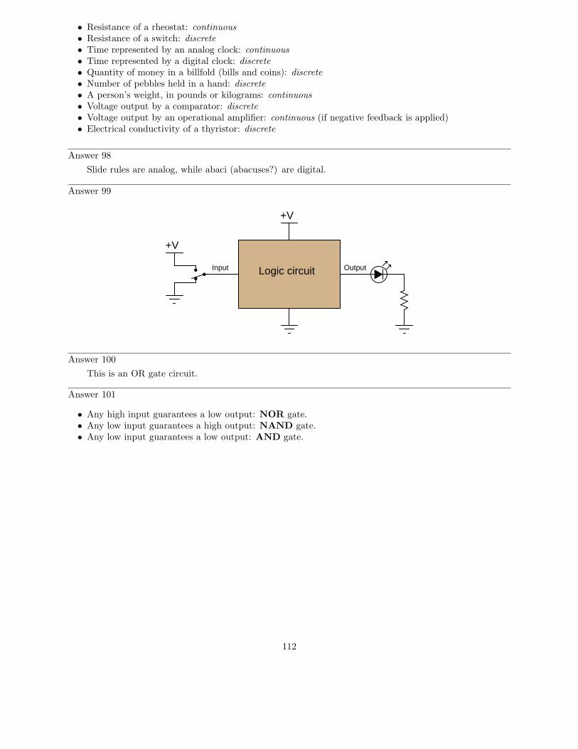
• Resistance of a rheostat: continuous• Resistance of a switch: discrete• Time represented by an analog clock: continuous• Time represented by a digital clock: discrete• Quantity of money in a billfold (bills and coins): discrete• Number of pebbles held in a hand: discrete• A person’s weight, in pounds or kilograms: continuous• Voltage output by a comparator: discrete• Voltage output by an operational amplifier: continuous (if negative feedback is applied)• Electrical conductivity of a thyristor: discrete
Answer 98
Slide rules are analog, while abaci (abacuses?) are digital.
Answer 99
+V
Logic circuitInput Output
+V
Answer 100
This is an OR gate circuit.
Answer 101
• Any high input guarantees a low output: NOR gate.• Any low input guarantees a high output: NAND gate.• Any low input guarantees a low output: AND gate.
112
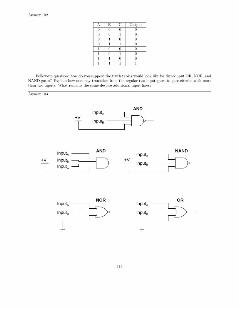
Answer 102
A B C Output0 0 0 00 0 1 00 1 0 00 1 1 01 0 0 01 0 1 01 1 0 01 1 1 1
Follow-up question: how do you suppose the truth tables would look like for three-input OR, NOR, andNAND gates? Explain how one may transition from the regular two-input gates to gate circuits with morethan two inputs. What remains the same despite additional input lines?
Answer 103
InputAInputB
InputA
InputB
InputA
InputB
InputA
InputB
InputC
AND NAND
NOR OR
InputA
InputB+V
AND
+V +V
113
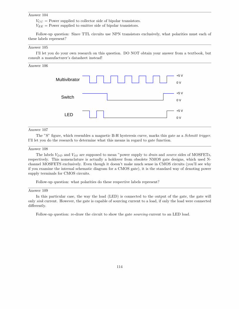
Answer 104
VCC = Power supplied to collector side of bipolar transistors.VEE = Power supplied to emitter side of bipolar transistors.
Follow-up question: Since TTL circuits use NPN transistors exclusively, what polarities must each ofthese labels represent?
Answer 105
I’ll let you do your own research on this question. DO NOT obtain your answer from a textbook, butconsult a manufacturer’s datasheet instead!
Answer 106
Multivibrator
Switch
LED
+5 V
0 V
+5 V
0 V
+5 V
0 V
Answer 107
The ”S” figure, which resembles a magnetic B-H hysteresis curve, marks this gate as a Schmitt trigger.I’ll let you do the research to determine what this means in regard to gate function.
Answer 108
The labels VDD and VSS are supposed to mean ”power supply to drain and source sides of MOSFETs,respectively. This nomenclature is actually a holdover from obsolete NMOS gate designs, which used N-channel MOSFETS exclusively. Even though it doesn’t make much sense in CMOS circuits (you’ll see whyif you examine the internal schematic diagram for a CMOS gate), it is the standard way of denoting powersupply terminals for CMOS circuits.
Follow-up question: what polarities do these respective labels represent?
Answer 109
In this particular case, the way the load (LED) is connected to the output of the gate, the gate willonly sink current. However, the gate is capable of sourcing current to a load, if only the load were connecteddifferently.
Follow-up question: re-draw the circuit to show the gate sourcing current to an LED load.
114
Answer 110
If you thought the answer to this question was, ”because MOSFET transistors are immune to damagefrom high-voltage transients,” you were wrong. If anything, MOSFETs are even more susceptible to damagefrom high-voltage transients than BJTs, given their thinly insulated gates.
The correct answer has to do with the bilateral (non polarity-sensitive) nature of MOSFETs whenconducting. Trace the direction of current through the relay coil while energized, and at the point in timewhen the gate output switches to a ”low” state, and you will understand why no commutating diode isnecessary in this circuit.
Answer 111
If an input or output of a CMOS gate circuit is driven above VDD, even momentarily, the circuit may”latch” like an SCR, causing VDD to become shorted to VSS internally. This is made possible by the wayCMOS transistors are manufactured on the integrated circuit’s substrate.
Challenge question: referencing a cross-sectional illustration of a CMOS gate integrated circuit, showthe ”SCR” formed by the transistors, and explain how it may be ”fired” by excessive input voltage to thegate.
Answer 112
The conductive foam makes the pins electrically common to one another, so no significant difference ofvoltage may appear between any two pins of the component.
Answer 113
One of the most significant differences is that in ladder diagrams, relay coils and relay contacts (thenormally-open contact in this diagram shown as a capacitor-like symbol) need not be drawn near each other.
Follow-up question: what do the two labels ”L1” and ”L2” represent?
Answer 114
The ”Run” switch is a normally-open pushbutton. Relay coil ”M1” is energized by this switch, andactuates three normally-open contacts (also labeled ”M1”) to send three-phase power to the motor. Notethat the details of the power supply are not shown in these diagrams. This is a common omission, done forthe sake of simplicity.
Answer 115
In this circuit, the motor will start once the ”Run” switch is actuated. When the ”Run” switch isreleased, the motor continues to run.
Follow-up question: this circuit has no ”stop” switch! What would have to be modified in the ladderlogic circuit to provide ”stop” control?
Answer 116
”Form C” is just another way of saying ”SPDT” with regard to switch or relay contacts.
Answer 117
In a properly designed system, with L2 grounded at the power source, this fault will result in a blownfuse when the pressure switch closes. In a circuit with L1 and L2 reversed, this same ground fault wouldenergize the relief solenoid, with or without the pressure switch’s ”permission.”
115
Answer 118
L1 L2
CR1A
B CR2
CR1 CR2
A and B
Answer 119
Lamp 1 Lamp 2A B Output
00
0 1
01
1 1
A B Output
00
0 1
01
1 1
1
0
0
0
1
0
0
0
Each of the lamps exhibits the behavior of a ”NOR” gate.
116
Notes
Notes 1
The purpose of this question is to get students thinking in terms of ”digital” quantities, which bytheir very nature are non-continuous. Since most electronics curricula focus on continuous quantities beforediscrete, it is good to have students reflect on the inherent simplicity of discrete circuitry and componentsafter having studied continuous (analog) circuitry.
Notes 2
This is a very simple concept, but worthwhile to cover in its own question just to be sure no studentsmisunderstand when the concept is later applied.
Notes 3
This question applies the concepts of ”high” and ”low” voltage signals to a simple transistor circuit,reviewing transistor operation in the process.
Notes 4
If students do not understand the purpose of these resistors after reading the question and researchingtheir texts, they should when they see the follow-up question. Discuss this question with your students, forthe concept of pulldown and pullup resistors is one that confuses some students.
Notes 5
This is one concept I have found many students have difficulty grasping, essentially because it involvesthe determination of a voltage drop between two points (the ”arrow” wire and ground). It is a spatial-relations problem, similar to Kirchhoff’s Voltage Law problems where students need to figure out how muchvoltage is between two specified points given voltage drops across several other pairs of points. Spend timewith your students discussing these circuits, because several of your students will probably not understandthis concept the first, second, or even third time through.
I strongly recommend students take the approach of a ”thought experiment” in determining the efficacyof each circuit shown here: analyze the output voltage (logic state) for each of the switch’s two positions.This simple approach usually helps clarify what each circuit does and why the ”improper” circuits do notwork.
Notes 6
It is important for students to understand that there is a certain range of voltage between a guaranteed”high” state and a guaranteed ”low” state that is indeterminate, and that this logic probe circuit is designedto indicate this range of voltage by turning neither LED on.
If time permits, discuss some of the benefits and drawbacks to using a voltmeter as a logic probe(especially a digital voltmeter where the display update time may be relatively long).
Notes 7
Your students should have no great difficulty identifying this particular logic gate if they have a gooddigital electronics reference book at their disposal.
Notes 8
Your students should have no great difficulty identifying this particular logic gate if they have a gooddigital electronics reference book at their disposal.
Notes 9
Your students should have no great difficulty identifying this particular logic gate if they have a gooddigital electronics reference book at their disposal.
117
Notes 10
Diode-resistor gate circuits such as this are rarely used in real digital circuitry because they have nocapacity to amplify weak input signals. They also have no capacity for signal inversion, rendering themincapable of representing a great many logic function types. Gates made from transistors are much preferredover diode-resistor technology.
Notes 11
In order to familiarize students with the standard logic gate types, I like to given them practice withidentification and truth tables each day. Students need to be able to recognize these logic gate types at aglance, or else they will have difficulty analyzing circuits that use them.
Notes 12
Have your students explain the operation of this TTL circuit, describing how the inverse logic state isgenerated at the output terminal, from a given input state.
Notes 13
TTL circuits are actually quite easy to analyze compared to analog amplifier circuits! Discuss withyour students the use of a dual-emitter transistor as a ”steering” diode network: this is a trick used by ICmanufacturers, to obtain three diodes for the ”price” of one transistor.
Notes 14
The very important concept of sourcing versus sinking is best understood from the perspective ofconventional current flow notation. The terms seem backward when electron flow notation is used to trackcurrent through the output transistor.
One point of confusion I’ve experienced among students is that current may go either direction (in orout) of a gate with totem-pole output transistors (able to sink or source current). Some students seem tohave a conceptual difficulty with current going in to the output terminal of a gate circuit, because theymistakenly associate the ”out” in output as being a reference to direction of current, rather than directionof information or data.
An analogy I’ve used to help students overcome this problem is that of two people carrying a long pole:
pole
Suppose these people are in a dark, noisy room, and they use the pole as a means of simplecommunication between them. For example, one person could tug on the pole to get the other person’sattention. Perhaps they could even develop a simple code system for communicating thoughts (1 tug =hello ; 2 tugs = good-bye ; 3 tugs = I think this is a silly way to communicate ; 4 tugs = let’s leave thisroom ; etc.). If one of the persons pushes on the pole rather than pulls on the pole to get the other person’sattention, does the direction of the pole’s motion change the direction of the communication between thetwo persons? Of course not. Well, then, does the direction of current through the output terminal of agate change the direction that information flows between two interconnected gates? Whether a gate sourcescurrent or sinks current to a load has no bearing on the ”output” designation of that gate terminal. Eitherway, the gate is still ”telling the load what to do” by exercising control over the load current.
118
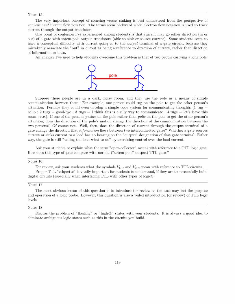
Notes 15
The very important concept of sourcing versus sinking is best understood from the perspective ofconventional current flow notation. The terms seem backward when electron flow notation is used to trackcurrent through the output transistor.
One point of confusion I’ve experienced among students is that current may go either direction (in orout) of a gate with totem-pole output transistors (able to sink or source current). Some students seem tohave a conceptual difficulty with current going in to the output terminal of a gate circuit, because theymistakenly associate the ”out” in output as being a reference to direction of current, rather than directionof information or data.
An analogy I’ve used to help students overcome this problem is that of two people carrying a long pole:
pole
Suppose these people are in a dark, noisy room, and they use the pole as a means of simplecommunication between them. For example, one person could tug on the pole to get the other person’sattention. Perhaps they could even develop a simple code system for communicating thoughts (1 tug =hello ; 2 tugs = good-bye ; 3 tugs = I think this is a silly way to communicate ; 4 tugs = let’s leave thisroom ; etc.). If one of the persons pushes on the pole rather than pulls on the pole to get the other person’sattention, does the direction of the pole’s motion change the direction of the communication between thetwo persons? Of course not. Well, then, does the direction of current through the output terminal of agate change the direction that information flows between two interconnected gates? Whether a gate sourcescurrent or sinks current to a load has no bearing on the ”output” designation of that gate terminal. Eitherway, the gate is still ”telling the load what to do” by exercising control over the load current.
Ask your students to explain what the term ”open-collector” means with reference to a TTL logic gate.How does this type of gate compare with normal (”totem pole” output) TTL gates?
Notes 16
For review, ask your students what the symbols VCC and VEE mean with reference to TTL circuits.Proper TTL ”etiquette” is vitally important for students to understand, if they are to successfully build
digital circuits (especially when interfacing TTL with other types of logic!).
Notes 17
The most obvious lesson of this question is to introduce (or review as the case may be) the purposeand operation of a logic probe. However, this question is also a veiled introduction (or review) of TTL logiclevels.
Notes 18
Discuss the problem of ”floating” or ”high-Z” states with your students. It is always a good idea toeliminate ambiguous logic states such as this in the circuits you build.
119
Notes 19
The utility of conventional flow notation (as opposed to electron flow) becomes especially apparent inthis answer, as the upper circuit is the one sourcing current and the lower circuit is the one sinking current.
As with operational amplifiers, I find it necessary to point out to some students that the inputs of alogic gate circuit do not sink or source load current. This fact underscores the need to supply DC power tothe logic gate for proper operation.
Notes 20
Ask your students why we might want to use a Darlington pair instead of a single transistor for the finaloutput ”driver” circuit. Also, ask them why we need to have a resistor connected between the gate outputand the transistor base. Why not just directly connect the gate’s output to the base of the transistor?
You might want to challenge your students with this question: ”Suppose the person who built thiscircuit used open-collector gates throughout. As a whole, it would not function, neither for lighting the LEDnor for ringing the bell. However, only one of the gates would need to have the standard ‘totem-pole’ outputin order for the circuit to function properly. Which gate is it?”
Notes 21
In order to familiarize students with the standard logic gate types, I like to given them practice withidentification and truth tables each day. Students need to be able to recognize these logic gate types at aglance, or else they will have difficulty analyzing circuits that use them.
Notes 22
Have your students explain the operation of this very simple MOSFET circuit, describing how theinverse logic state is generated at the output terminal, from a given input state. Discuss with your studentsthe simplicity of the CMOS inverter, especially contrasted against a TTL inverter circuit.
Notes 23
It is important that students realize these ”protection” diodes do not allow circuit designers and buildersto disregard good design practices with impunity. Ask your students, in each case, how each protection diodeaccomplishes its task of protecting the MOSFETs from damage. Does this mean the gate circuit will be ableto withstand abnormal conditions indefinitely? Why or why not?
Notes 24
Discuss the problem of ”floating” or ”high-Z” states with your students, especially in the context ofCMOS. What is it about the nature of a CMOS circuit that makes floating inputs especially troublesome?Ask your students to contrast this against floating TTL inputs.
Notes 25
CMOS logic gate circuits are the easiest of all the gates to analyze internally! Discuss with your studentswhy the second-from-the-top MOSFET uses an independent substrate connection (as opposed to making itcommon with the source, as usual).
Notes 26
This question gets students in the habit of consulting datasheets to obtain information on logic gatecircuits. Datasheets are a wealth of technical information, and students absolutely have to become adept atreferencing them to obtain the information they need to build and troubleshoot logic circuits.
Notes 27
The most obvious lesson of this question is to introduce (or review as the case may be) the purpose andoperation of a logic probe. However, this question is also a veiled introduction (or review) of CMOS logiclevels.
120
Notes 28
I strongly suggest you take the time to implement an improved-security design with your students. Apractical project such as this sparks a lot of interest, and thus provides an excellent learning opportunity.
Not only does this question afford the opportunity to analyze logic gates, but it also provides a contextin which to review optocouplers and TRIACs. Ask your students what the labels ”L1” and ”L2” mean, withreference to AC power circuitry, as well.
Notes 29
Texas Instruments publishes an excellent application report (SCHA004 – October 2002) comparingbuffered versus unbuffered CMOS logic gates. I highly recommend it for your reference.
Notes 30
High-speed CMOS was a very important developmental milestone in digital logic gate technology, andit is essential for modern (2005) students of electronics to be aware of since it is so widely used. In manyways it blends the best of the old TTL and CMOS worlds, with few disadvantages.
Notes 31
This question provides a good opportunity to review electromechanical relays: how they work, whatthey are used for, etc.
Notes 32
Ask your students to identify what arrangement the relay contacts are connected it: series or parallel?Does this contact arrangement make sense with regard to the established function of the gate?
Notes 33
Ask your students to identify what arrangement the relay contacts are connected it: series or parallel?Does this contact arrangement make sense with regard to the established function of the gate?
Notes 34
If students don’t raise this point on their own, direct their attention to the relay coil and contactsymbols. What looks strange here? What sort of electrical component are students familiar associating withthe ”CR1” contact symbol? Does it make sense to use this symbol to symbolize a normally-open switch(relay) contact? If we wished to show a normally-closed relay contact instead, how would we modify thediagram?
Notes 35
Many students find it confusing that relay contacts and coils need not be drawn next to one another ina ladder logic diagram, because it is so different from the schematic diagrams they are accustomed to. Thenon-necessity of proximity in a ladder logic diagram does have its advantages, though! It is simply a matterof getting used to a new way of drawing things.
Notes 36
Discuss with students the fact that relay coils and contacts need not be located near each other in ladderdiagrams. While this may be confusing at times, it is a very flexible feature of ladder logic notation, becauseit gives the author the freedom to locate relay contacts where it makes the most visual sense in the ”output”rung of the diagram, without having to coordinate locations of coil and contact as is generally necessary intraditional schematic diagrams. Instead, relay contacts are associated with their respective coils by label, notby proximity on the diagram.
121
Notes 37
Many students find the ”line-through-the-contact” a very intuitive way to represent normally-closedrelay contacts. Be sure to emphasize that the diagonal line, as well as the name normally-closed, does notrefer to any given state of the contact, but rather to the contact’s resting state when the relay coil is de-energized. I have seen teachers put a diagonal line through a relay contact symbol on a ladder logic diagramto indicate the state of the contact being closed by energization of the coil, during the process of explaininghow a circuit functioned. This is wrong, as it confuses the concept of contacts being normally-closed withthe concept of contacts simply being (energized) closed.
Notes 38
In order to familiarize students with standard switch contact configurations, I like to given them practicewith identification and truth tables each day. Students need to be able to recognize these ladder logic sub-circuits at a glance, or else they will have difficulty analyzing more complex relay circuits that use them.
Notes 39
This circuit provides students with an opportunity to analyze a simple latch: a system that ”remembers”prior switch actuations by holding a ”state” (either set or reset; latched or unlatched). A simple motorstart/stop circuit such as this is about as simple as latch circuits get.
Students should be able to immediately comprehend the benefit of using nice, neat, structured ladderdiagrams when they see the tangled mess of wires in a real motor control circuit. And this is not even acomplex motor control circuit! It takes very little imagination to think of something even uglier than this,and what a task it would be to troubleshoot such a circuit without the benefit of a ladder diagram forguidance.
Notes 40
Discuss with your students why load devices are never to be connected in series. What would be theeffect of doing so? Have them answer this question in terms of normal operation, and also in terms ofoperation given a failure condition in one of the series-connected load devices.
Notes 41
In order to familiarize students with the standard logic gate types, I like to given them practice withidentification and truth tables each day. Students need to be able to recognize these logic gate types at aglance, or else they will have difficulty analyzing circuits that use them.
Notes 42
It should be noted that totem-pole TTL gates can actually source far more current than what isadvertised without sustaining damage. The severe limitation on sourcing current is more a function ofstaying within the permitted output voltage margins for TTL than it is a function of chip heating. Thus,you may generally use a totem-pole TTL gate to source 20 mA to an LED without harm, though the ”high”state output voltage (when the LED is lit) will be significantly below the acceptable threshold for a TTLgate input.
Notes 43
I purposely omitted answers for this question, not only because I want students to do the research ontheir own, but also because it makes it more interesting when students consult different datasheets and derivedifferent answers (for different logic ”families”)!
Notes 44
For the relatively simple digital circuits that beginning students build, fan-out is rarely a problem. Morelikely is that students will try to drive a load that is too ”heavy,” causing the same voltage level problem.
122
Notes 45
The given answer cuts to the heart of the matter, but I want students to elaborate on the details.Specifically, why each of the three acceptable paralleled circuits avoids risk of damage. Make sure you spendadequate time discussing ”tri-state” outputs as well. Ask your students to explain what the three outputstates of a ”tri-state” gate are.
Notes 46
This question, to be answered properly, involves more than just a definition of ”noise margin.” Studentsmust first discover that there is a difference between voltage compliance levels for gate inputs versus outputs,then recognize that the difference constitutes a ”margin” that imposed AC voltage (”noise”) must not exceed.They must then present their answer in terms of manufacturer specifications, obtained in datasheets. Insummary, there is a lot of research that must occur to answer this question, but the results will be worth it!
Notes 47
I purposely omitted answers for this question, not only because I want students to do the research ontheir own, but also because it makes it more interesting when students consult different datasheets and derivedifferent answers (for different logic ”families”)!
Notes 48
For the relatively simple digital circuits that beginning students build, fan-out is rarely a problem. Morelikely is that students will try to drive a load that is too ”heavy,” causing the same voltage level problem.
Notes 49
This question, to be answered properly, involves more than just a definition of ”noise margin.” Studentsmust first discover that there is a difference between voltage compliance levels for gate inputs versus outputs,then recognize that the difference constitutes a ”margin” that imposed AC voltage (”noise”) must not exceed.They must then present their answer in terms of manufacturer specifications, obtained in datasheets. Insummary, there is a lot of research that must occur to answer this question, but the results will be worth it!
Notes 50
Discuss this trend with your students, citing examples from industry literature if possible. Be sure toask your students why lower operating voltages reduces power dissipation (with reference to Joule’s Law,please!), and also why this reduces noise margins.
Notes 51
The choice of diodes is not critical in a circuit where the inputs come from manually actuated switches.Neither is the choice of resistor sizes (10 kΩ) works just fine, especially when the only thing loading theoutput is the student’s logic probe or voltmeter.
Notes 52
It needs to be understood that this is an AND gate only if you consider the ”0” and ”1” states as definedby voltage levels with respect to ground, and not by switch actuation. Many students assume an actuated(pushed) switch is a ”1” input and a de-actuated (unpushed) switch is a ”0” input. Not necessarily so! Inthis circuit, the switches are connecting inputs to ground. This means a closed (actuated) switch provides alow (0) input state, while an open (unactuated) switch provides a high (1) input state.
123
Notes 53
The purpose of this exercise is for students to research what type of IC this is (from the given partnumber for U1), its pinout, and then predict and prove its operation using truth tables to document theresults. You, as the instructor, may select any 14-pin CMOS or TTL logic IC that you wish. Students areto draw the logic gate symbol within the rectangle of U1, then connect that symbol to the input switchesand output LED.
It needs to be understood that the ”0” and ”1” states are defined by voltage levels with respect toground, and not by switch actuation. Many students assume an actuated (pushed) switch is a ”1” inputand a de-actuated (unpushed) switch is a ”0” input. Not necessarily so! In this circuit, the switches areconnecting inputs to ground. This means a closed (actuated) switch provides a low (0) input state, while anopen (unactuated) switch provides a high (1) input state.
Notes 54
The transition from ladder logic diagram to actual relay wiring is a confusing one for many students.This is what I consider to be the most significant learning objective of this exercise: figuring out how tobuild the circuit, not necessarily understanding the logical function of it.
Notes 55
Something omitted from too many basic digital electronics texts is a thorough discussion on interfacingIC logic gates with high-power devices, usually using relays. This is a very important subject, however,because many devices we wish to control with digital logic circuits are too power-hungry to directly drivewith the logic gate outputs! Here, students get the opportunity to experiment with how to make a logic gate(CMOS, preferably) drive an electric motor.
One component value you may wish to have your students size themselves is resistor R3, being the basecurrent limiting resistor for transistor Q1. It must be sized such that the transistor is saturated with thegate output in the HIGH state, yet not allowing so much base current that the transistor becomes damaged.Figuring out an appropriate size for this resistor is a very practical exercise, forcing students to reviewtransistor theory (calculations with β) as well as consider characteristics of the load.
It may be advisable (especially if the logic gate is TTL and requires a precise 5.0 volt power supply) tohave a separate source of power for the electric motor.
Notes 56
The purpose of this assessment rubric is to act as a sort of “contract” between you (the instructor) andyour student. This way, the expectations are all clearly known in advance, which goes a long way towarddisarming problems later when it is time to grade.
Notes 57
The purpose of this question is to approach the domain of circuit troubleshooting from a perspective ofknowing what the fault is, rather than only knowing what the symptoms are. Although this is not necessarilya realistic perspective, it helps students build the foundational knowledge necessary to diagnose a faultedcircuit from empirical data. Questions such as this should be followed (eventually) by other questions askingstudents to identify likely faults based on measurements.
Notes 58
The purpose of this question is to approach the domain of circuit troubleshooting from a perspective ofknowing what the fault is, rather than only knowing what the symptoms are. Although this is not necessarilya realistic perspective, it helps students build the foundational knowledge necessary to diagnose a faultedcircuit from empirical data. Questions such as this should be followed (eventually) by other questions askingstudents to identify likely faults based on measurements.
124
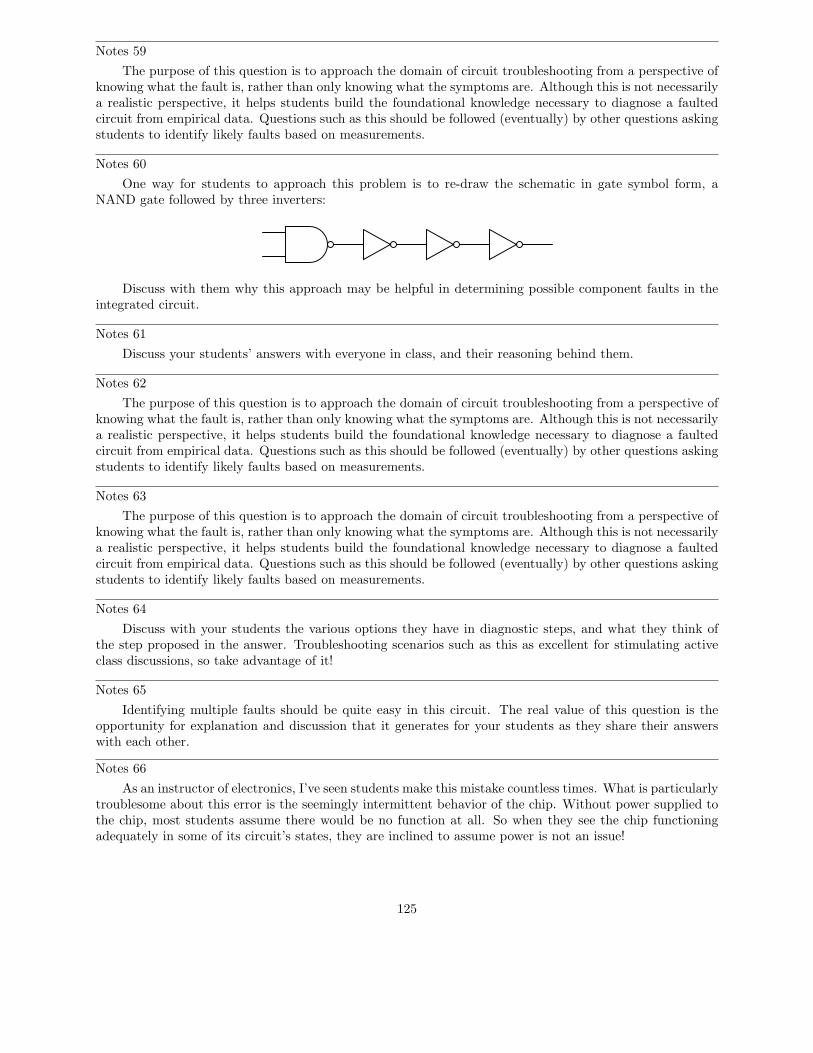
Notes 59
The purpose of this question is to approach the domain of circuit troubleshooting from a perspective ofknowing what the fault is, rather than only knowing what the symptoms are. Although this is not necessarilya realistic perspective, it helps students build the foundational knowledge necessary to diagnose a faultedcircuit from empirical data. Questions such as this should be followed (eventually) by other questions askingstudents to identify likely faults based on measurements.
Notes 60
One way for students to approach this problem is to re-draw the schematic in gate symbol form, aNAND gate followed by three inverters:
Discuss with them why this approach may be helpful in determining possible component faults in theintegrated circuit.
Notes 61
Discuss your students’ answers with everyone in class, and their reasoning behind them.
Notes 62
The purpose of this question is to approach the domain of circuit troubleshooting from a perspective ofknowing what the fault is, rather than only knowing what the symptoms are. Although this is not necessarilya realistic perspective, it helps students build the foundational knowledge necessary to diagnose a faultedcircuit from empirical data. Questions such as this should be followed (eventually) by other questions askingstudents to identify likely faults based on measurements.
Notes 63
The purpose of this question is to approach the domain of circuit troubleshooting from a perspective ofknowing what the fault is, rather than only knowing what the symptoms are. Although this is not necessarilya realistic perspective, it helps students build the foundational knowledge necessary to diagnose a faultedcircuit from empirical data. Questions such as this should be followed (eventually) by other questions askingstudents to identify likely faults based on measurements.
Notes 64
Discuss with your students the various options they have in diagnostic steps, and what they think ofthe step proposed in the answer. Troubleshooting scenarios such as this as excellent for stimulating activeclass discussions, so take advantage of it!
Notes 65
Identifying multiple faults should be quite easy in this circuit. The real value of this question is theopportunity for explanation and discussion that it generates for your students as they share their answerswith each other.
Notes 66
As an instructor of electronics, I’ve seen students make this mistake countless times. What is particularlytroublesome about this error is the seemingly intermittent behavior of the chip. Without power supplied tothe chip, most students assume there would be no function at all. So when they see the chip functioningadequately in some of its circuit’s states, they are inclined to assume power is not an issue!
125
Notes 67
This question is not really a troubleshooting question per se, but the principles involved in successfullydetermining the presence or absence of voltage are critically important to being able to troubleshoot simplecircuits using a voltmeter.
I have found that the concept of electrically common points is most helpful when students first learnto relate voltage drop with continuity (breaks or non-breaks) in a circuit. You might want them to identifywhich points in this circuit are electrically common to one another (in either or both switch positions).
Notes 68
Challenge your students to think of other methods which could be used to check the switch’s continuity.There is often more than one way to perform a certain check of component function, if you are knowledgeablein electrical theory and creative in your use of test equipment!
Notes 69
What we have here is an exercise in Aristotelian logic. In either scenario (points in a circuit, oranimals), statement 2 is the converse of statement 1, while statement 3 is the inverse and statement 4 is thecontrapositive. Only the contrapositive of a statement is guaranteed to share the same truth value as theoriginal statement.
This is no esoteric exercise. Rather, it is a hard-learned fact: many students mistakenly think thatbecause there is guaranteed to be no voltage between electrically common points in a circuit, then theabsence of voltage between two points must mean those two points are electrically common to each other!This is not necessarily true, because situations exist where two points may not be electrically common, yetstill have no voltage between them. Electrical commonality is just one way that two points can have zerovoltage between them, not the only way!
The contrapositive of this rule, however, is a valuable troubleshooting tool: if there is substantialvoltage measured between two points in a circuit, then we know without a doubt that those two points arenot electrically common to each other!
Notes 70
Not only does this question introduce students to the various levels of shock current necessary to inducedeleterious effects in the (healthy) human body, but it also serves as a good exercise for Ohm’s Law, and forintroducing (or reviewing) the concept of series resistances.
For the morbidly curious, Charles Dalziel’s experimentation conducted at the University of California(Berkeley) began with a state grant to investigate the bodily effects of sub-lethal electric current. His testingmethod was as follows: healthy male and female volunteer subjects were asked to hold a copper wire in onehand and place their other hand on a round, brass plate. A voltage was then applied between the wire andthe plate, causing electrons to flow through the subject’s arms and chest. The current was stopped, thenresumed at a higher level. The goal here was to see how much current the subject could tolerate and stillkeep their hand pressed against the brass plate. When this threshold was reached, laboratory assistantsforcefully held the subject’s hand in contact with the plate and the current was again increased. The subjectwas asked to release the wire they were holding, to see at what current level involuntary muscle contraction(tetanus) prevented them from doing so. For each subject the experiment was conducted using DC andalso AC at various frequencies. Over two dozen human volunteers were tested, and later studies on heartfibrillation were conducted using animal subjects.
Given that Dalziel tested subjects for the effects of a hand-to-hand shock current path, his data doesnot precisely match the scenario I show in the schematic diagram (hand-to-foot). Therefore, the calculatedvoltages for various hand-to-foot shock conditions are approximate only.
126
Notes 71
One suggestion for approaching this question is to ask your students to identify which of the powersource conductors is ”hot” and which one is ”neutral,” then identify which points in the circuit are electricallycommon to either one or the other source conductors.
Notes 72
The italicized text was taken directly from Puget Sound Energy’s April 2005 ”Energywise” mail flyer.The points brought up were, I thought, very appropriate for discussion of electrical safety and theory.Personally, I question the suggestion of shuffling on both feet. I would suspect that running full-speed,where only one foot touches the ground at a time, and where you would leave the dangerous area faster,would be the safest option. I would be very interested to see if there is any scientific test data available onthis subject!
Notes 73
Discuss with your students the need for good communication between all people performing maintenancework on large and (potentially) dangerous systems. Tags are an integral part of this communication.
Notes 74
Real-life story here: I was once asked to place an electric motor back in service after it had been lockedout for a few days, for routine maintenance. I removed my lock and tag, and was just about to turn thebreaker back on, when better judgment prevailed and I decided to first check the job site. Lo and behold,there, still working on the motor coupling, were two contract employees completely oblivious to the situation.They had not been told there was a circuit breaker to secure power to that electric motor, nor were theyaware that they needed to lock it out in addition to everyone else on the project! Had I turned that circuitbreaker back on, the motor could have started up and severely injured at least one of them!
Lesson to be learned: if you are performing work on a piece of equipment, you need to have your lockand your tag securing energy to that equipment. Never, ever trust someone else to lock-out and tag-out acircuit breaker for you!
Notes 75
As a follow-up to this question, you might wish to draw current-carrying wires at different angles, andwith current moving in different directions, as practice problems for your students to draw the correspondingarrow points and tails.
Notes 76
Clamp-on meters are very useful pieces of test equipment, but they must be used properly. I have seenmany people make the mistake of clamping one of these ammeters around multiple wires when trying tomeasure the amount of current through only one. If you have any clamp-on meters in your classroom, haveyour students set up a simple circuit like this and prove the validity of the concept.
Notes 77
This is an exercise in algebraic substitution. Students are not likely to find this equation anywhere, sothey’ll have to create it from a combination of two other equations.
Notes 78
The purpose of this question is twofold: to get students to see that a ferromagnetic material such asiron is much more permeable (less ”reluctant”) than air, but that the great gains in B realized by iron tendto disappear as soon as saturation sets in. Once the iron is saturated, the gains in B for equal advances inH are the same as for air. That is, the dB
dHfor iron is equal to the dB
dHfor air once the iron is saturated.
127
Notes 79
This is simply a quantitative application of Faraday’s Law. There is no significance to the fact that themagnetic flux is increasing rather than decreasing. The only effect this would have on the induced voltageis its polarity.
Notes 80
This phenomenon is difficult to demonstrate without a very powerful magnet. However, if you havesuch apparatus available in your lab area, it would make a great piece for demonstration!
One practical way I’ve demonstrated Lenz’s Law is to obtain a rare-earth magnet (very powerful!), setit pole-up on a table, then drop an aluminum coin (such as a Japanese Yen) so it lands on top of the magnet.If the magnet is strong enough and the coin is light enough, the coin will gently come to rest on the magnetrather than hit hard and bounce off.
A more dramatic illustration of Lenz’s Law is to take the same coin and spin it (on edge) on a tablesurface. Then, bring the magnet close to the edge of the spinning coin, and watch the coin promptly cometo a halt, without contact between the coin and magnet.
Another illustration is to set the aluminum coin on a smooth table surface, then quickly move themagnet over the coin, parallel to the table surface. If the magnet is close enough, the coin will be ”dragged”a short distance as the magnet passes over.
In all these demonstrations, it is significant to show to your students that the coin itself is not magnetic.It will not stick to the magnet as an iron or steel coin would, thus any force generated between the coin andmagnet is strictly due to induced currents and not ferromagnetism.
Notes 81
An easy way I find to remember Lenz’s Law is to interpret is as opposition to change. The coil willtry to become a magnet that fights the motion. A good way to get students thinking along these lines isto ask them, ”What magnetic polarity would the coil have to assume (in each case) to resist the magnet’srelative motion?” In other words, if the magnet moves closer to the coil, the coil will ”magnetize” so as topush against the magnet. If the magnet moves away from the coil, the coil will ”magnetize” so as to attractthe magnet.
Notes 82
As always, it is more important to be able to apply a term to a real-life example than it is to memorizea definition for that term. In my experience, many students prefer to memorize definitions for terms ratherthan to go through the trouble of understanding how those terms apply to real life. Make sure studentsrealize just how and why these AC terms apply to a waveform such as this.
Notes 83
I purposely omit the velocity of light, as well as the time/distance/velocity equation, so that studentswill have to do some simple research this calculate this value. Neither of these concepts is beyond high-schoollevel science students, and should pose no difficulty at all for college-level students to find on their own.
Notes 84
Students must properly interpret the oscilloscope’s display, then correctly convert to RMS units, inorder to obtain the correct answer for this question.
128
Notes 85
Many electronics students I’ve talked to seem to think that the RMS value of a waveform is always√
2
2,
no matter what the waveshape. Not true, as evidenced by the answer for this question!
Students must properly interpret the oscilloscope’s display in order to obtain the correct answer for thisquestion. The ”conversion” to RMS units is really non-existent, but I want students to be able to explainwhy it is and not just memorize this fact.
Notes 86
This question is nothing more than an exercise in Lissajous figure interpretation.
Notes 87
Not only is the quotation funny, but it is startling as well, especially to those of us who were bornwithout any computers in our homes at all, much less multiple personal computers.
A point I wish to make in having students research the term ”microcontroller” is to see that mostof the computers in existence are not of the variety one ordinarily thinks of by the label ”computer.”Those doorknob computers – as well as engine control computers in automobiles, kitchen appliances, cellulartelephones, biomedical implants, talking birthday cards, and other small devices – are much smaller andmuch more specialized than the ”general purpose” computers people use at their desks to write documentsor surf the internet. They are the silent, unseen side of the modern ”computer revolution,” and in many waysare more appropriate for beginning students of digital electronics to explore than their larger, general-purposecounterparts.
Notes 88
Note that I did not bother to explain my extremely terse answer. This is a subject I desire students tothink long and hard about, for the real answer(s) to this question are the reasons driving all development ofprogrammable digital devices.
Notes 89
The purpose of this question is for students to realize that the microcontroller must be told to ”loop”through the light blinking instructions. Really, this is just an illustration of loops in a practical context.
In case you’re wondering why I write in pseudocode, here are a few reasons:
• No prior experience with programming required to understand pseudocode
• It never goes out of style
• Hardware independent
• No syntax errors
If I had decided to showcase code that would actually run in a microcontroller, I would be dooming thequestion to obsolescence. This way, I can communicate the spirit of the program without being chained toan actual programming standard. The only drawback is that students will have to translate my pseudocodeto real code that will actually run on their particular MCU hardware, but that is a problem guaranteed forsome regardless of which real programming language I would choose.
Of course, I could have taken the Donald Knuth approach and invented my own (imaginary) hardwareand instruction set . . .
Notes 90
The purpose of this question is for students to understand what a ”WHILE” loop represents in practicalterms: a loop with condition(s). It also contrasts conditional looping against unconditional looping, andshows how both play a part in interactive systems such as this one.
In case you’re wondering why I write in pseudocode, here are a few reasons:
129
• No prior experience with programming required to understand pseudocode• It never goes out of style• Hardware independent• No syntax errors
If I had decided to showcase code that would actually run in a microcontroller, I would be dooming thequestion to obsolescence. This way, I can communicate the spirit of the program without being chained toan actual programming standard. The only drawback is that students will have to translate my pseudocodeto real code that will actually run on their particular MCU hardware, but that is a problem guaranteed forsome regardless of which real programming language I would choose.
Of course, I could have taken the Donald Knuth approach and invented my own (imaginary) hardwareand instruction set . . .
Notes 91
Although this logic function could have been implemented easier and cheaper in hard-wired (gate) logic,the purpose is to get students to think of performing logical operations by a sequenced set of instructionsinside a programmable device (the MCU). This is a conceptual leap, basic but very important.
In case you’re wondering why I write in pseudocode, here are a few reasons:
• No prior experience with programming required to understand pseudocode• It never goes out of style• Hardware independent• No syntax errors
If I had decided to showcase code that would actually run in a microcontroller, I would be dooming thequestion to obsolescence. This way, I can communicate the spirit of the program without being chained toan actual programming standard. The only drawback is that students will have to translate my pseudocodeto real code that will actually run on their particular MCU hardware, but that is a problem guaranteed forsome regardless of which real programming language I would choose.
Of course, I could have taken the Donald Knuth approach and invented my own (imaginary) hardwareand instruction set . . .
Notes 92
Although this logic function could have been implemented easier and cheaper in hard-wired (gate) logic,the purpose is to get students to think of performing logical operations by a sequenced set of instructionsinside a programmable device (the MCU). This is a conceptual leap, basic but very important.
In case you’re wondering why I write in pseudocode, here are a few reasons:
• No prior experience with programming required to understand pseudocode• It never goes out of style• Hardware independent• No syntax errors
If I had decided to showcase code that would actually run in a microcontroller, I would be dooming thequestion to obsolescence. This way, I can communicate the spirit of the program without being chained toan actual programming standard. The only drawback is that students will have to translate my pseudocodeto real code that will actually run on their particular MCU hardware, but that is a problem guaranteed forsome regardless of which real programming language I would choose.
Of course, I could have taken the Donald Knuth approach and invented my own (imaginary) hardwareand instruction set . . .
130

Notes 93
Although this logic function could have been implemented easier and cheaper in hard-wired (gate) logic,the purpose is to get students to think of performing logical operations by a sequenced set of instructionsinside a programmable device (the MCU). This is a conceptual leap, basic but very important.
In case you’re wondering why I write in pseudocode, here are a few reasons:
• No prior experience with programming required to understand pseudocode• It never goes out of style• Hardware independent• No syntax errors
If I had decided to showcase code that would actually run in a microcontroller, I would be dooming thequestion to obsolescence. This way, I can communicate the spirit of the program without being chained toan actual programming standard. The only drawback is that students will have to translate my pseudocodeto real code that will actually run on their particular MCU hardware, but that is a problem guaranteed forsome regardless of which real programming language I would choose.
Of course, I could have taken the Donald Knuth approach and invented my own (imaginary) hardwareand instruction set . . .
Notes 94
Although this logic function could have been implemented easier and cheaper in hard-wired (gate) logic,the purpose is to get students to think of performing logical operations by a sequenced set of instructionsinside a programmable device (the MCU). This is a conceptual leap, basic but very important.
In case you’re wondering why I write in pseudocode, here are a few reasons:
• No prior experience with programming required to understand pseudocode• It never goes out of style• Hardware independent• No syntax errors
If I had decided to showcase code that would actually run in a microcontroller, I would be dooming thequestion to obsolescence. This way, I can communicate the spirit of the program without being chained toan actual programming standard. The only drawback is that students will have to translate my pseudocodeto real code that will actually run on their particular MCU hardware, but that is a problem guaranteed forsome regardless of which real programming language I would choose.
Of course, I could have taken the Donald Knuth approach and invented my own (imaginary) hardwareand instruction set . . .
131
Notes 95
Although this logic function could have been implemented easier and cheaper in hard-wired (gate) logic,the purpose is to get students to think of performing logical operations by a sequenced set of instructionsinside a programmable device (the MCU). This is a conceptual leap, basic but very important.
In case you’re wondering why I write in pseudocode, here are a few reasons:
• No prior experience with programming required to understand pseudocode• It never goes out of style• Hardware independent• No syntax errors
If I had decided to showcase code that would actually run in a microcontroller, I would be dooming thequestion to obsolescence. This way, I can communicate the spirit of the program without being chained toan actual programming standard. The only drawback is that students will have to translate my pseudocodeto real code that will actually run on their particular MCU hardware, but that is a problem guaranteed forsome regardless of which real programming language I would choose.
Of course, I could have taken the Donald Knuth approach and invented my own (imaginary) hardwareand instruction set . . .
Notes 96
Although this logic function could have been implemented easier and cheaper in hard-wired (gate) logic,the purpose is to get students to think of performing logical operations by a sequenced set of instructionsinside a programmable device (the MCU). This is a conceptual leap, basic but very important.
In case you’re wondering why I write in pseudocode, here are a few reasons:
• No prior experience with programming required to understand pseudocode• It never goes out of style• Hardware independent• No syntax errors
If I had decided to showcase code that would actually run in a microcontroller, I would be dooming thequestion to obsolescence. This way, I can communicate the spirit of the program without being chained toan actual programming standard. The only drawback is that students will have to translate my pseudocodeto real code that will actually run on their particular MCU hardware, but that is a problem guaranteed forsome regardless of which real programming language I would choose.
Of course, I could have taken the Donald Knuth approach and invented my own (imaginary) hardwareand instruction set . . .
Notes 97
The purpose of this question is to get students thinking in terms of ”digital” quantities, which bytheir very nature are non-continuous. It is important to note that the concepts of continuous and discretequantities are not limited to electronics, but are found in a variety of places in every-day life.
It should be noted that some of these determinations are subjective. The voltage output by a comparatormay be considered discrete on a large time scale, but there is a measurable transition from ”high” voltageto ”low” voltage in which the output voltage is somewhere between full saturation limits.
Notes 98
One challenge to answering this question is for (young) students to figure out what a slide rule is!
132
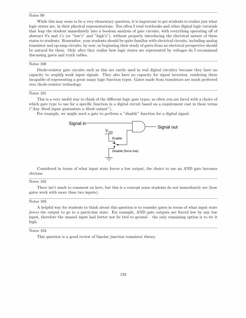
Notes 99
While this may seem to be a very elementary question, it is important to get students to realize just whatlogic states are, in their physical representations. Too often I read textbooks and other digital logic tutorialsthat leap the student immediately into a boolean analysis of gate circuits, with everything operating off ofabstract 0’s and 1’s (or ”low’s” and ”high’s”), without properly introducing the electrical nature of thesestates to students. Remember, your students should be quite familiar with electrical circuits, including analogtransistor and op-amp circuits, by now, so beginning their study of gates from an electrical perspective shouldbe natural for them. Only after they realize how logic states are represented by voltages do I recommenddiscussing gates and truth tables.
Notes 100
Diode-resistor gate circuits such as this are rarely used in real digital circuitry because they have nocapacity to amplify weak input signals. They also have no capacity for signal inversion, rendering themincapable of representing a great many logic function types. Gates made from transistors are much preferredover diode-resistor technology.
Notes 101
This is a very useful way to think of the different logic gate types, as often you are faced with a choice ofwhich gate type to use for a specific function in a digital circuit based on a requirement cast in these terms(”Any blank input guarantees a blank output”).
For example, we might need a gate to perform a ”disable” function for a digital signal:
VDD
Signal inSignal out
Enable
Disable (force low)
Considered in terms of what input state forces a low output, the choice to use an AND gate becomesobvious.
Notes 102
There isn’t much to comment on here, but this is a concept some students do not immediately see (howgates work with more than two inputs).
Notes 103
A helpful way for students to think about this question is to consider gates in terms of what input stateforces the output to go to a particular state. For example, AND gate outputs are forced low by any lowinput, therefore the unused input had better not be tied to ground – the only remaining option is to tie ithigh.
Notes 104
This question is a good review of bipolar junction transistor theory.
133
Notes 105
This true story was told to me by one of my former students, who had some previous experience withelectronics maintenance prior to enrolling in my class. The moral of this story, of course, is the sensitivity ofTTL logic circuits to power supply voltage variations. This will (and should!) surprise many of your students,who are probably used to seeing the rather wide voltage limits of opamps and other analog circuitry.
Notes 106
Many students find the waveform analysis of digital circuits intimidating at first, until they understandthat it is nothing more than a graphical representation of ”0” and ”1” logic states over time. Ask yourstudents to share their ”tips” on how to relate waveforms to truth tables, and in particular how theyanswered this particular question.
Just for fun, you might want to ask your students to identify where in time the toggle switch is open,and where it is closed. Some students may answer backwards to this question, if they haven’t carefullyconsidered how the toggle switch is connected in this circuit!
Notes 107
Schmitt trigger gates are indispensable for certain logic circuit applications. It is important that studentsrecognize their function and utility.
Incidentally, this question provides a good opportunity to review magnetic hysteresis curves, since it’sprobably been awhile since students last studied electromagnetism theory!
Notes 108
Ahhh, the vestiges of yesterday’s technology! What can I say? Sometimes terms ”stick” even when itmakes little sense for them to.
134
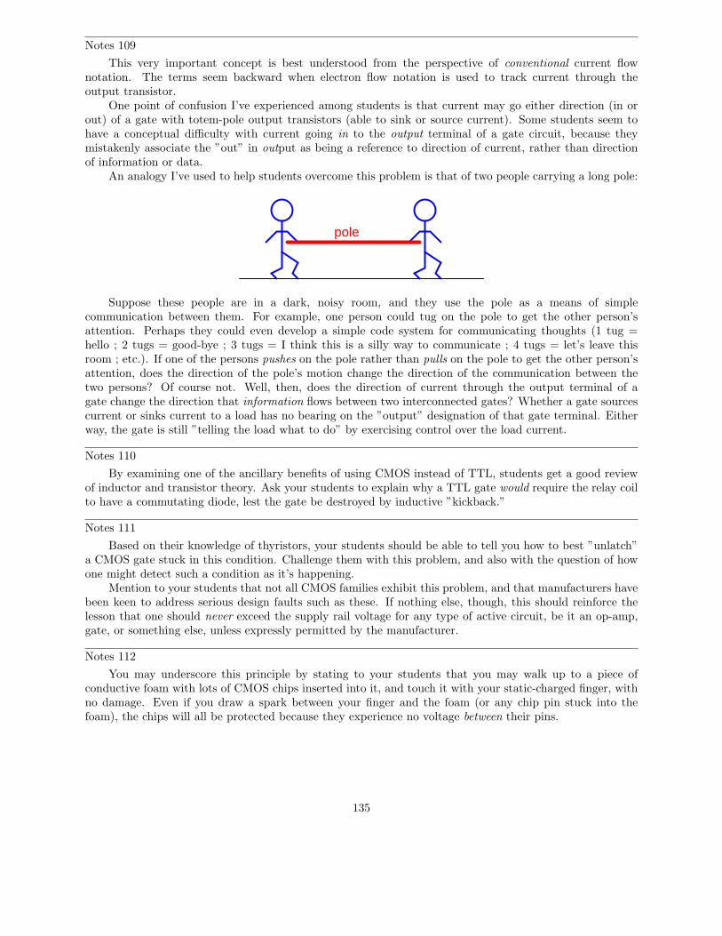
Notes 109
This very important concept is best understood from the perspective of conventional current flownotation. The terms seem backward when electron flow notation is used to track current through theoutput transistor.
One point of confusion I’ve experienced among students is that current may go either direction (in orout) of a gate with totem-pole output transistors (able to sink or source current). Some students seem tohave a conceptual difficulty with current going in to the output terminal of a gate circuit, because theymistakenly associate the ”out” in output as being a reference to direction of current, rather than directionof information or data.
An analogy I’ve used to help students overcome this problem is that of two people carrying a long pole:
pole
Suppose these people are in a dark, noisy room, and they use the pole as a means of simplecommunication between them. For example, one person could tug on the pole to get the other person’sattention. Perhaps they could even develop a simple code system for communicating thoughts (1 tug =hello ; 2 tugs = good-bye ; 3 tugs = I think this is a silly way to communicate ; 4 tugs = let’s leave thisroom ; etc.). If one of the persons pushes on the pole rather than pulls on the pole to get the other person’sattention, does the direction of the pole’s motion change the direction of the communication between thetwo persons? Of course not. Well, then, does the direction of current through the output terminal of agate change the direction that information flows between two interconnected gates? Whether a gate sourcescurrent or sinks current to a load has no bearing on the ”output” designation of that gate terminal. Eitherway, the gate is still ”telling the load what to do” by exercising control over the load current.
Notes 110
By examining one of the ancillary benefits of using CMOS instead of TTL, students get a good reviewof inductor and transistor theory. Ask your students to explain why a TTL gate would require the relay coilto have a commutating diode, lest the gate be destroyed by inductive ”kickback.”
Notes 111
Based on their knowledge of thyristors, your students should be able to tell you how to best ”unlatch”a CMOS gate stuck in this condition. Challenge them with this problem, and also with the question of howone might detect such a condition as it’s happening.
Mention to your students that not all CMOS families exhibit this problem, and that manufacturers havebeen keen to address serious design faults such as these. If nothing else, though, this should reinforce thelesson that one should never exceed the supply rail voltage for any type of active circuit, be it an op-amp,gate, or something else, unless expressly permitted by the manufacturer.
Notes 112
You may underscore this principle by stating to your students that you may walk up to a piece ofconductive foam with lots of CMOS chips inserted into it, and touch it with your static-charged finger, withno damage. Even if you draw a spark between your finger and the foam (or any chip pin stuck into thefoam), the chips will all be protected because they experience no voltage between their pins.
135
Notes 113
Discuss these diagrams with your students, noting any significant advantages and disadvantages of eachconvention.
In reference to the challenge question, the symbols ”L1” and ”L2” are very common designations forAC power conductors. Be sure your students have researched this and know what these labels mean!
Notes 114
Discuss with your students the sources of electrical power for both circuits here: the relay control circuitand the motor itself. Challenge your students to explore this concept by asking them the following questions:
• Are the two sources necessarily the same?• How does the convention of linking relay coils with contacts by name (rather than by dashed lines and
proximity) in ladder diagrams benefit multiple-source circuits such as this one?• Do these circuits even have to be drawn on the same page?
Notes 115
This circuit is known as a latching circuit, because it ”latches” in the ”on” state after a momentaryaction. The contact in parallel with the ”Run” switch is often referred to as a seal-in contact, because it”seals” the momentary condition of the Run switch closure after that switch is de-actuated.
The follow-up question of how we may make the motor stop running is a very important one. Spendtime with your students discussing this practical design problem, and implement a solution.
Notes 116
When I first heard of a switch having ”Form C” contacts, I had absolutely no idea what it meant. Iwas quite familiar with ”single-pole, double-throw,” but not this new term. Different industries often usedifferent terms for describing the same things. Your students should be made aware that there is a tendencyfor people to become ”isolated” within their respective industries or fields of expertise, to the point wherethey may be unaware of alternative terms for the same things (Form-C versus SPST is a good exampleof this). Your students may even find themselves misjudged by others for not knowing the peculiar andspecialized terms used within certain industries, when they first obtain employment. In many ways it is akinto the misunderstandings arising when different cultures meet: people have the general tendency to thinktheir way of doing things is the only way. Bridging such cultural divides requires patience, humility, andtact.
Notes 117
The ultimate purpose of this question is not to ascertain the effects of a particular fault so much as itis to derive a general rule regarding the construction of industrial control circuits. Students should be ableto see the benefits of having L2 (the grounded power rail) on the right-hand side of the circuit, but can theyinduce the general safety principle to be applied in all control circuits? What is ”special” about having L2on the right-hand side of the ladder diagram?
Notes 118
Discuss with students the fact that relay coils and contacts need not be located near each other in ladderdiagrams. While this may be confusing at times, it is a very flexible feature of ladder logic notation, becauseit gives the author the freedom to locate relay contacts where it makes the most visual sense in the ”output”rung of the diagram, without having to coordinate locations of coil and contact as is generally necessary intraditional schematic diagrams. Instead, relay contacts are associated with their respective coils by label, notby proximity on the diagram.
136

Notes 119
This question provides a good opportunity for students to practice analyzing relay logic circuits, andit also foreshadows DeMorgan’s Theorem in its dual implementation of the NOR function. Note to yourstudents how more than one contact is being used on control relays CR1 and CR2!
137


![[XLS] · Web view1 140 2 140 3 140 4 140 5 140 6 140 7 140 8 140 9 140 10 140 11 140 12 140 13 140 14 140 15 140 16 140 17 140 18 140 19 140 20 140 21 140 22 140 23 140 24 140 25](https://img.pdfslide.net/doc/110x75/5b0e34b97f8b9a96478b4bbf/xls-view1-140-2-140-3-140-4-140-5-140-6-140-7-140-8-140-9-140-10-140-11-140-12.jpg)
![PARTS LIST - Billigkoste.dk · 00 140 6894 000 1 rectifier [1] 7 140 6423 500 1 kabel eu l=15m black 7 140 6423 530 1 cord uk l 15m 7 140 3859 630 1 cord set kit uz964 us/tw 7 140](https://img.pdfslide.net/doc/110x75/61019d92c4826339540599bc/parts-list-00-140-6894-000-1-rectifier-1-7-140-6423-500-1-kabel-eu-l15m-black.jpg)