Embed Size (px)
Citation preview

Power ElectronicSystemsLaboratory
1
EM Simulations using the PEEC Method -Case Studies in Power Electronics
Andreas Müsing
Swiss Federal Institute of Technology (ETH) ZürichPower Electronic Systems Laboratory
www.pes.ee.ethz.ch

Power ElectronicSystemsLaboratory
2
Outline
■ Motivation: The need for EM simulators in Power Electronics
■ Application Case Studies• Conducted Emission Noise Prediction• PEEC-Based Numerical Optimization of Position Sensors• Switching Transient Current Shaping
■ Generating a Quadrilateral Mesh: “Paving”
■ Partial Element Calculations
■ Outlook

Power ElectronicSystemsLaboratory
3
■ Circuit simulation is daily business for PE engineer■ Increasing switching frequencies and fast transients require the
inclusion of parasitics and EM effects■ Device and system integration requires knowledge of EM behaviour■ Development of prototypes is expensive trend to virtual prototyping
The need for EM Simulators in Power Electronics
Power ElectronicSystemsLaboratory
4
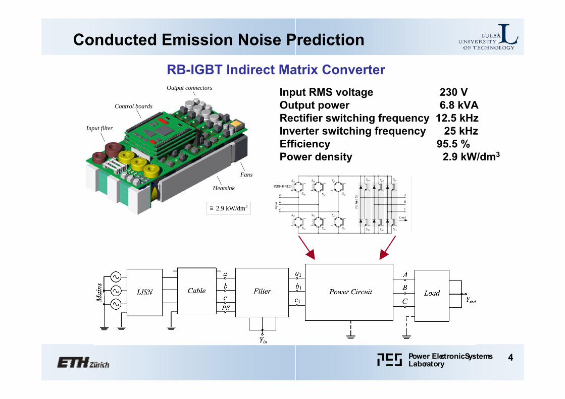
Input filter
Heatsink
Fans
Output connectors
Control boards
2.9 kW/dm3=~
Input RMS voltage 230 VOutput power 6.8 kVARectifier switching frequency 12.5 kHzInverter switching frequency 25 kHzEfficiency 95.5 %Power density 2.9 kW/dm3
RB-IGBT Indirect Matrix Converter
Conducted Emission Noise Prediction

Power ElectronicSystemsLaboratory
5
RB-IGBT Indirect Matrix Converter Model
103 104 105 106 107
Frequency [Hz]
10-2
103
104
105
10-1
Impe
danc
e[Ω
]
102
102 108
Capacitance between two conductors
100
101
Measurement
Inductance of a single conductor
Model Measurement
Model
103 104 105 106 107
Frequency [Hz]
100
103
104
105
101
Impe
danc
e[Ω
]
102
102 108
Impedance across all inductors (measurement)
Impedance from one input terminal to PE (model)
Impedance from one input terminal to PE (measurement)
Impedance across all inductors (model)
cr
+−
i c
G(t)
ssv
ceu
C(u)
behavioral switch model layout parasitics
“backward” modeling from impedance measurements

Power ElectronicSystemsLaboratory
6
PCB Layout Parasitics Calculation
■ Java based program for the generation of PEEC models from PCB CAD data
■ PEEC solver calculates PCB track impedances, i.e. parasitic capacitances, inductances and mutual inductances
subsequent refinement of IMC circuit model
Parasitics Extraction (inductive and capacitive) using PEEC Simulation:
6 Layer IMC PCB layout

Power ElectronicSystemsLaboratory
7
Simulation results (CM and DM)
Conducted Emission spectrumcommon mode and differential mode
■ TD simulation of 1 mains period■ Timestep: 10 ns■ Simulation time:
approx. 4 hours on a 3 GHz PC with 1 GB of RAM
Simulation properties:■ Excellent agreement of CE level (CM and DM)
up to 5 MHz■ Deviation for f > 5 MHz probably
influenced by higher order parasitics( EMI filter couplings, heat sink, …)
Results:

Power ElectronicSystemsLaboratory
8
Outline
■ Motivation: The need for EM simulators in Power Electronics
■ Application Case Studies• Conducted Emission Noise Prediction• PEEC-Based Numerical Optimization of Position Sensors• Switching Transient Current Shaping
■ Generating a Quadrilateral Mesh: “Paving”
■ Partial Element Calculations
■ Outlook

Power ElectronicSystemsLaboratory
9
PEEC-Based Numerical Optimization of Position Sensors
Context: Active Magnetic Bearing System for Mega-Speed Drives (> 500000 rpm)
576 Hz
4682 Hz
Power and control electronics of the motor
Power and control electronicsof the magnetic bearings
Challenges:• Materials → mechanical stress due to high rotational speeds• Position control and damping of rotor eigenmodes
FE simulation of rotor eigenmodes:

Power ElectronicSystemsLaboratory
10
Radial Position Sensors
Eddy Current Sensors:
• Radial sensors integrated into PCB• Excitation coil generates concentric
magnetic field around the rotor• Magnetic field rejected by eddy
currents within rotor material→ Field concentration between rotor
and excitation coil.
• Difference in the field strength is detectedby four sensing coils.

Power ElectronicSystemsLaboratory
11
Eddy Current Position Sensor Modeling
Screenshot of Sensor Model in the PEEC Design Environment
Power ElectronicSystemsLaboratory
12
Simulation Results

Power ElectronicSystemsLaboratory
13
Simulation Results

Power ElectronicSystemsLaboratory
14
Layout Optimization
■ Maximization of sensor output signal • Frequency dependence• Variation of winding ratios• Testing of different layouts• Influence of feed lines
■ Optimization hardly possible withoutthe help of simulation
alternative eddy current sensor layouts

Power ElectronicSystemsLaboratory
15
Outline
■ Motivation: The need for EM simulators in Power Electronics
■ Application Case Studies• Conducted Emission Noise Prediction• PEEC-Based Numerical Optimization of Position Sensors• Switching Transient Current Shaping
■ Generating a Quadrilateral Mesh: “Paving”
■ Partial Element Calculations
■ Outlook

Power ElectronicSystemsLaboratory
16
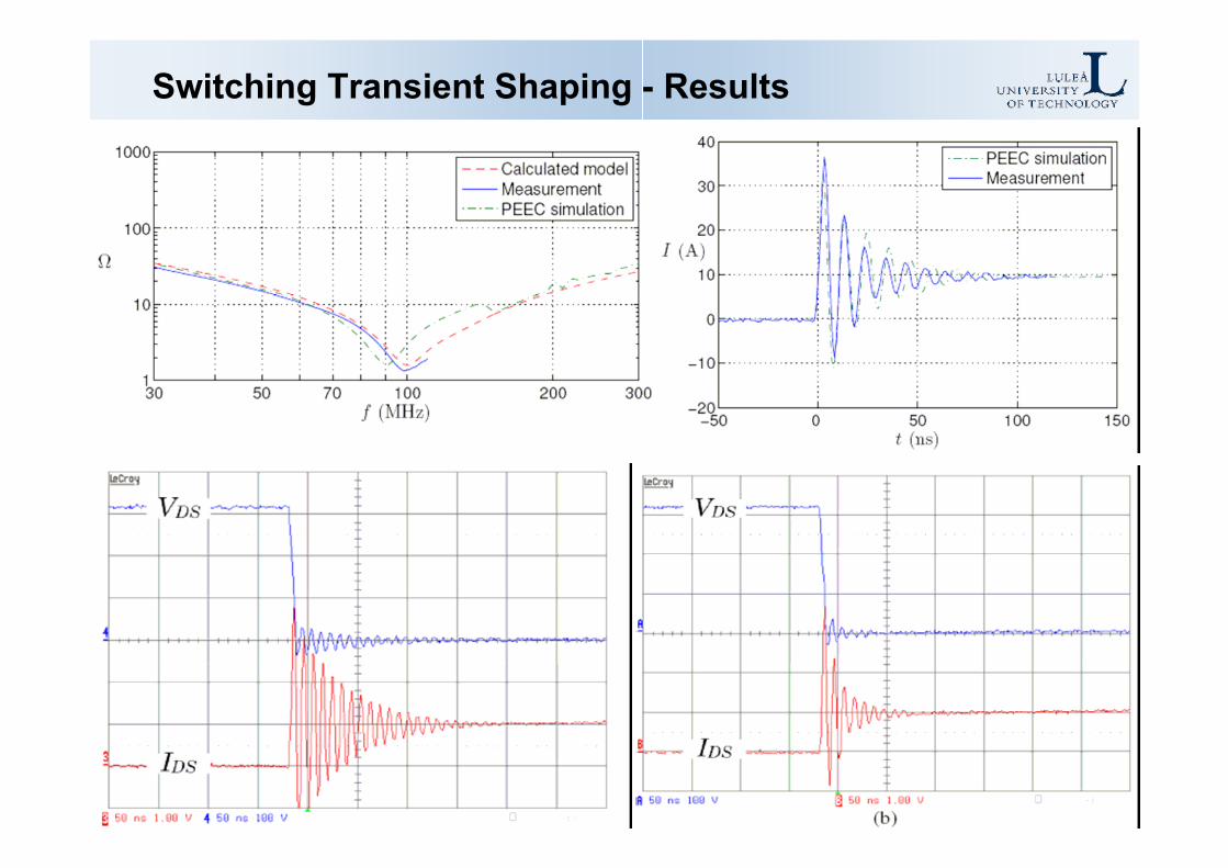
Switching Transient Shaping
Boost converter• 2.5 MHz Switching Frequency• 30 kV / μs voltage slope• 2 kA / μs current slope• strong ringing during transistor
turn-on

Power ElectronicSystemsLaboratory
17
Switching Transient Shaping
How to damp the ringing?• RC snubber circuit?
• better: magnetically coupled damping layer inside PCB

Power ElectronicSystemsLaboratory
18
Switching Transient Shaping – PEEC model
Power ElectronicSystemsLaboratory
19
Switching Transient Shaping - Results

Power ElectronicSystemsLaboratory
20
Outline
■ Motivation: The need for EM simulators in Power Electronics
■ Application Case Studies• Conducted Emission Noise Prediction• PEEC-Based Numerical Optimization of Position Sensors• Switching Transient Current Shaping
■ Generating a Quadrilateral Mesh: “Paving”
■ Partial Element Calculations
■ Outlook

Power ElectronicSystemsLaboratory
21
Generating a Quadrilateral Mesh: „Paving“

Power ElectronicSystemsLaboratory
22
Outline
■ Motivation: The need for EM simulators in Power Electronics
■ Application Case Studies• Conducted Emission Noise Prediction• PEEC-Based Numerical Optimization of Position Sensors• Switching Transient Current Shaping
■ Generating a Quadrilateral Mesh: “Paving”
■ Partial Element Calculations
■ Outlook

Power ElectronicSystemsLaboratory
23
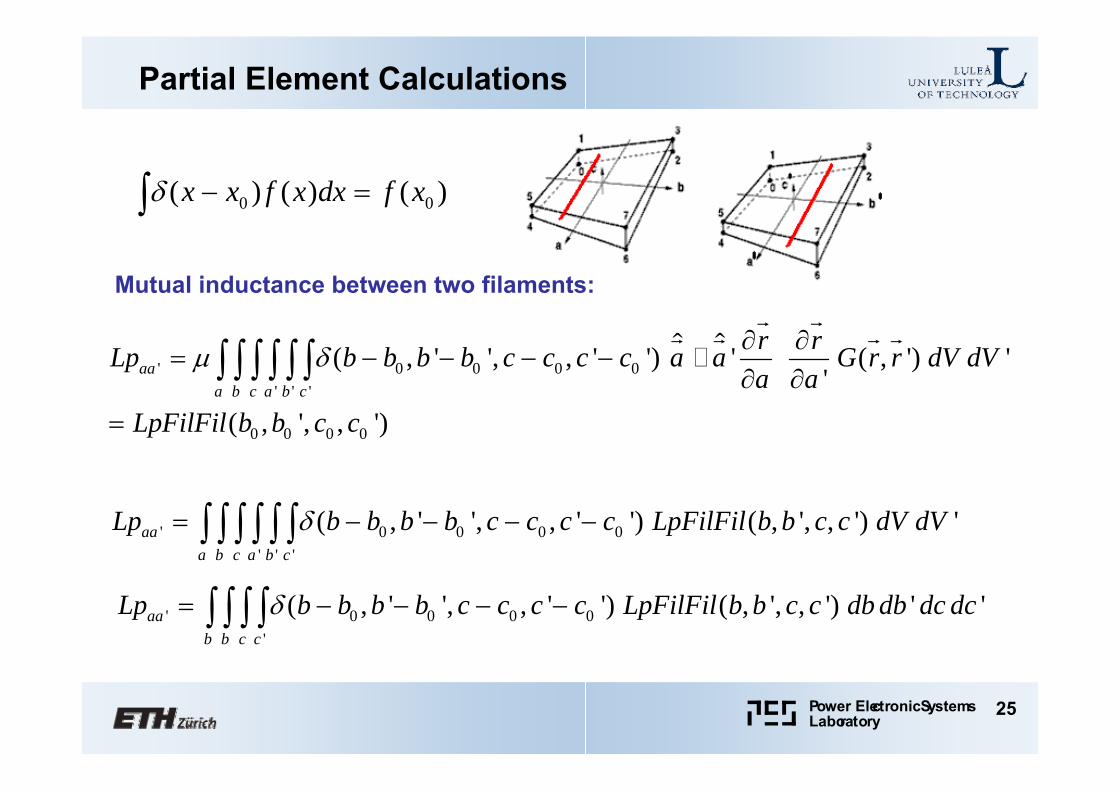
Partial Element Calculations
Problem: calculation of partial elements (L and P) for nonorthogonal geometries
• orthogonal case: analytic formulas• general: multidimensional integration is required• high computational effort due tofull matrices
• accuracy critical TD stability
11 12 13 14
22
33
44
... ... ...
... ... ...
... ... ...
L L L LL
LL
L
⎛ ⎞⎜ ⎟⎜ ⎟=⎜ ⎟⎜ ⎟⎝ ⎠
$ $'
' ' '
' ( ( , , ), ( ', ', ')) ' ' ''
1( ( , , ), ( ', ', '))4 '
aaa b c a b c
r rLp a a G r a b c r a b c da db dc da db dca a
G r a b c r a b cr r
μ
π
∂ ∂=
∂ ∂
=−
∫ ∫ ∫ ∫ ∫ ∫r r
r r r r
r rr r

Power ElectronicSystemsLaboratory
24
Partial Element Calculations
Solution approach: analytic formulas for arbitrary alignedFilaments order reduction of integration possible
1 2 1 4
3 4 2 3
((( ) arctanh ( ) arctanh
arctanh arctanh ) cos( ),sin( )
m lLpFilFil l mR R R R
m l dR R R R
μ ν
μ ν εε
= + ⋅ + + ⋅+ +
Ω− ⋅ − ⋅ −
+ +
2 2 2 2
1 12 2 2 2
1 1
cos( ) ( )( )sin cos( ) ( ) sinarctan arctansin( ) sin( )
cos( ) sin cos( ) ( )sin arctan arctansin( ) sin( )
d l m d ldR dR
d d mdR dR
ε μ ν ε ε μ ν εε ε
ε μν ε ε μ ν εε ε
+ + + + +Ω = −
+ + ⋅ ++ −
Power ElectronicSystemsLaboratory
25
Partial Element Calculations
$ $' 0 0 0 0
' ' '
0 0 0 0
( , ' ', , ' ') ' ( , ') ''
( , ', , ')
aaa b c a b c
r rLp b b b b c c c c a a G r r dV dVa a
LpFilFil b b c c
μ δ ∂ ∂= − − − −
∂ ∂
=
∫ ∫ ∫ ∫ ∫ ∫r r
r r r r
0 0( ) ( ) ( )x x f x dx f xδ − =∫
' 0 0 0 0' ' '
( , ' ', , ' ') ( , ', , ') 'aaa b c a b c
Lp b b b b c c c c LpFilFil b b c c dV dVδ= − − − −∫ ∫ ∫ ∫ ∫ ∫
Mutual inductance between two filaments:
' 0 0 0 0'
( , ' ', , ' ') ( , ', , ') ' 'aab b c c
Lp b b b b c c c c LpFilFil b b c c db db dc dcδ= − − − −∫ ∫ ∫ ∫
Power ElectronicSystemsLaboratory
26
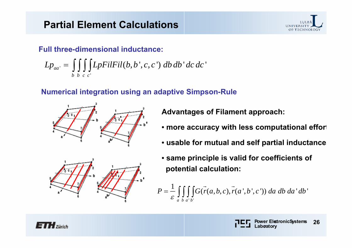
Partial Element Calculations
''
( , ', , ') ' 'aab b c c
Lp LpFilFil b b c c db db dc dc= ∫ ∫ ∫ ∫Full three-dimensional inductance:
Numerical integration using an adaptive Simpson-Rule
Advantages of Filament approach:
• more accuracy with less computational effort
• usable for mutual and self partial inductances
• same principle is valid for coefficients of potential calculation:
' '
1 ( ( , , ), ( ', ', ')) ' 'a b a b
P G r a b c r a b c da db da dbε
= ∫ ∫ ∫ ∫r r

Power ElectronicSystemsLaboratory
27
Partial Element Calculations
Benchmark: Aircoil-Reactor

Power ElectronicSystemsLaboratory
28
Partial Element Calculations: Benchmark
Partial element computation time:
analytic < 10 sec
Gauss-Legendre integration 6 min
filament integration 1 min

Power ElectronicSystemsLaboratory
29
Outlook: Where do we want to go tomorrow?
PEEC Simulation Environment
Circuit Simulator
3D FEM Thermal Solver
Macro-Modeling
PEEC simulation environments builds submodels:• EMI filter components: HF resonances, parasitic couplings ( inductive and capacitive )
• Full 3D EM design modeling environment ( PCB‘s, heat sink, busbars,discrete components, power modules, cables )
Power ElectronicSystemsLaboratory
30
Outline
■ Motivation: The need for EM simulators in Power Electronics
■ Application Case Studies• Conducted Emission Noise Prediction• PEEC-Based Numerical Optimization of Position Sensors• Switching Transient Current Shaping
■ Generating a Quadrilateral Mesh: “Paving”
■ Partial Element Calculations
■ Outlook

Power ElectronicSystemsLaboratory
31
Thank you for
your attention !


![Mozambique PEEC[1]](https://img.pdfslide.net/doc/110x75/5571fdc4497959916999e379/mozambique-peec1.jpg)