Embed Size (px)
Citation preview

A Course Material on
Embedded and Real Time Systems

UNIT- 1INTRODUCTION TO EMBEDDED COMPUTING
1. COMPLEX SYSTEMS AND MICROPROCESSORS
What is an embedded computer system? Loosely defined, it is any device that includes aprogrammable computer but is not itself intended to be a general-purpose computer. Thus, a PCis not itself an embedded computing system, although PCs are often used to build embeddedcomputing systems. But a fax machine or a clock built from a microprocessor is an embeddedcomputing system.
This means that embedded computing system design is a useful skill for many types of productdesign. Automobiles, cell phones, and even household appliances make extensive use ofmicroprocessors. Designers in many fields must be able to identify where microprocessors canbe used, design a hardware platform with I/O devices that can support the required tasks, andimplement software that performs the required processing.
Computer engineering, like mechanical design or thermodynamics, is a fundamental disciplinethat can be applied in many different domains. But of course, embedded computing systemdesign does not stand alone.
Many of the challenges encountered in the design of an embedded computing system are notcomputer engineering—for example,they may be mechanical or analog electrical problems. Inthis book we are primarily interested in the embedded computer itself, so we will concentrate onthe hardware and software that enable the desired functions in the final product.
1.1 Embedding Computers
Computers have been embedded into applications since the earliest days of computing. Oneexample is the Whirlwind, a computer designed at MIT in the late 1940s and early 1950s.Whirlwind was also the first computer designed to support real-time operation and wasoriginally conceived as a mechanism for controlling an aircraft simulator.
Even though it was extremely large physically compared to today’s computers (e.g., it containedover 4,000 vacuum tubes), its complete design from components to system was attuned to theneeds of real-time embedded computing.
The utility of computers in replacing mechanical or human controllers was evident from thevery beginning of the computer era—for example, computers were proposed to control chemicalprocesses in the late 1940s.
A microprocessor is a single-chip CPU. Very large scale integration (VLSI) stet the acronym isthe name technology has allowed us to put a complete CPU on a single chip since 1970s, butthose CPUs were very simple.
The first microprocessor, the Intel 4004, was designed for an embedded application, namely, acalculator. The calculator was not a general-purpose computer—it merely provided basicarithmetic functions. However, Ted Hoff of Intel realized that a general-purpose computer

programmed properly could implement the required function, and that the computer-on-a-chipcould then be reprogrammed for use in other products as well.
Since integrated circuit design was (and still is) an expensive and time consuming process, theability to reuse the hardware design by changing the software was a key breakthrough.
The HP-35 was the first handheld calculator to perform transcendental functions [Whi72]. Itwas introduced in 1972, so it used several chips to implement the CPU, rather than a single-chipmicroprocessor.
However, the ability to write programs to perform math rather than having to design digitalcircuits to perform operations like trigonometric functions was critical to the successful designof the calculator.
Automobile designers started making use of the microprocessor soon after single-chip CPUsbecame available.
The most important and sophisticated use of microprocessors in automobiles was to control theengine: determining when spark plugs fire, controlling the fuel/air mixture, and so on. Therewas a trend toward electronics in automobiles in general—electronic devices could be used toreplace the mechanical distributor.
But the big push toward microprocessor-based engine control came from two nearlysimultaneous developments: The oil shock of the 1970s caused consumers to place much highervalue on fuel economy, and fears of pollution resulted in laws restricting automobile engineemissions.
The combination of low fuel consumption and low emissions is very difficult to achieve; tomeet these goals without compromising engine performance, automobile manufacturers turnedto sophisticated control algorithms that could be implemented only with microprocessors.
Microprocessors come in many different levels of sophistication; they are usually classified bytheir word size. An 8-bit microcontroller is designed for low-cost applications and includes on-board memory and I/O devices; a 16-bit microcontroller is often used for more sophisticatedapplications that may require either longer word lengths or off-chip I/O and memory; and a 32-bit RISC microprocessor offers very high performance for compwuwwta.atninoaunn-ivienrztietyn.cosmive applications.
Given the wide variety of microprocessor types available, it should be no surprise thatmicroprocessors are used in many ways. There are many household uses of microprocessors.The typical microwave oven has at least one microprocessor to control oven operation.
Many houses have advanced thermostat systems, which change the temperature level at varioustimes during the day. The modern camera is a prime example of the powerful features that canbe added under microprocessor control.
Digital television makes extensive use of embedded processors. In some cases, specializedCPUs are designed to execute important algorithms—an example is the CPU designed for audio

processing in the SGS Thomson chip set for DirecTV [Lie98]. This processor is designedto efficiently implement programs for digital audio decoding.
A programmable CPU was used rather than a hardwired unit for two reasons: First, it madethe system easier to design and debug; and second, it allowed the possibility of upgrades andusing the CPU for other purposes.
A high-end automobile may have 100 microprocessors, but even inexpensive cars today use40 microprocessors. Some of these microprocessors do very simple things such as detectwhether seat belts are in use. Others control critical functions such as the ignition and brakingsystems.
BMW 850i brake and stability control system:
The BMW 850i was introduced with a sophisticated system for controlling the wheels ofthe car. An antilock brake system (ABS) reduces skidding by pumping the brakes.
An automatic stability control (ASC +T) system intervenes with the engine duringmaneuvering to improve the car’s stability. These systems actively control critical systems ofthe car; as control systems, they require inputs from and output to the automobile.
Let’s first look at the ABS. The purpose of an ABS is to temporarily release the brake ona wheel when it rotates too slowly—when a wheel stops turning, the car starts skidding andbecomes hard to control. It sits between the hydraulic pump, which provides power tothe brakes, and the brakes themselves as seen in the following diagram. This hookup allowsthe ABS system to modulate the brakes in order to keep the wheels from locking.
The ABS system uses sensors on each wheel to measure the speed of the wheel. Thewheel speeds are used by the ABS system to determine how to vary the hydraulic fluidpressure toprevent the wheels from skidding.
The ASC + T system’s job is to control the engine power and the brake to improve the car’sstability during maneuvers.
The ASC+T controls four different systems: throttle, ignition timing, differential brake, and(on automatic transmission cars) gear shifting.
The ASC + T can be turned off by the driver, which can be important when operating withtire snow chains.
The ABS and ASC+ T must clearly communicate because the ASC + T interacts with thebrake system. Since the ABS was introduced several years earlier than the ASC + T, it wasimportant to be able to interface ASC + T to the existing ABS module, as well as to otherexisting electronic modules.
The engine and control management units include the electronically controlled throttle, digital enginemanagement, and electronic transmission control. The ASC + T control unit has two

microprocessors on two printed circuit boards, one of which concentrates on logic-relevant componentsand the other on performance-specific components.
1.1.1 Characteristics of Embedded ComputingApplications
Embedded computing is in many ways much more demanding than the sort of programsthat you may have written for PCs or workstations. Functionality is important in both general-purposecomputing and embedded computing, but embedded applications must meet many other constraintsaswell.
On the one hand, embedded computing systems have to provide sophisticated functionality:
■ Complex algorithms: The operations performed by the microprocessor may be verysophisticated. For example, the microprocessor that controls an automobile engine must performcomplicated filtering functions to optimize the performance of the car while minimizing pollution andfuel utilization.
■ User interface: Microprocessors are frequently used to control complex user interfaces that mayinclude multiple menus and many options. The moving maps in Global Positioning System (GPS)navigation are good examples of sophisticated user interfaces.
To make things more difficult, embedded computing operations must often be performedto meet deadlines:■ Real time: Many embedded computing systems have to perform in real time— if the data is notready by a certain deadline, the system breaks. In some cases, failure to mewewtw.anndauenaivderlzitny.ecomis unsafeand can even endanger lives. In other cases, missing a deadline does not create safety problems butdoes create unhappy customers—missed deadlines in printers, for example, can result in scrambledpages.
■ Multirate: Not only must operations be completed by deadlines, but many embedded computingsystems have several real-time activities going on at the same time. They may simultaneously controlsome operations that run at slow rates and others that run at high rates. Multimedia applications areprime examples of multirate behavior. The audio and video portions of a multimedia stream run atvery different rates, but they must remain closely synchronized. Failure to meet a deadline oneither the audio or video portions spoils the perception of the entire presentation.
Costs of various sorts are also veryimportant:
■ Manufacturing cost: The total cost of building the system is very important in many cases.Manufacturing cost is determined by many factors, including the type of microprocessor used, theamount of memory required, and the types of I/O devices.■ Power and energy: Power consumption directly affects the cost of the hardware, since a largerpower supply may be necessary. Energy consumption affects battery life, which is important in manyapplications, as well as heat consumption, which can be important even in desktop applications.

1.2DESIGN EXAMPLE: MODEL TRAIN CONTROLLER
In order to learn how to use UML to model systems, we will specify a simple system, amodel train controller, which is illustrated in Figure 1.2.The user sends messages to the trainwith a control box attached to the tracks.
The control box may have familiar controls such as a throttle, emergency stop button, and so on.Since the train receives its electrical power from the two rails of the track, the control box cansend signals to the train over the tracks by modulating the power supply voltage. As shownin the figure, the control panel sends packets over the tracks to the receiver on the train.
The train includes analog electronics to sense the bits being transmitted and a control system toset the train motor’s speed and direction based on thosecommands.
Each packet includes an address so that the console can control several trains on the sametrack; the packet also includes an error correction code (ECC) to guard against transmissionerrors. This is a one-way communication system the model train cannot send commands backto the user.
We start by analyzing the requirements for the train control system.We will base our systemon a real standard developed for model trains.We then develop two specifications: a simple,high- level specification and then a more detailed specification.
1.2.1 Requirements
Before we can create a system specification, we have to understwawnwd.antnhaeunirveerqziutyi.croemments.
Here is a basic set of requirements for the system:
The console shall be able to control up to eight trains on a single track.
The speed of each train shall be controllable by a throttle to at least 63 different levels ineach direction (forward and reverse).
There shall be an inertia control that shall allow the user to adjust the responsiveness of thetrain to commanded changes in speed. Higher inertia means that the train responds moreslowly to a change in the throttle, simulating the inertia of a large train. The inertia control willprovide at least eight different levels.
There shall be an emergency stop button.
An error detection scheme will be used to transmit messages.

We can put the requirements into chart format:
NamePurposeInputsOutputsFunctions
PerformanceManufacturing costPowerPhysical size and weight
Model train controllerControl speed of up to eight model trainsThrottle, inertia setting, emergency stop, train numberTrain control signalsSet engine speed based upon inertia settings; respond toemergency stopCan update train speed at least 10 times per second$5010W (plugs into wall)Console should be comfortable for two hands,approximate size of standard keyboard; weight<2 pounds
We will develop our system using a widely used standard for model train control. We coulddevelop our own train control system from scratch, but basing our system upon a standard hasseveral advantages in this case: It reduces the amount of work we have to do and it allows us touse a wide variety of existing trains and other pieces of equipment.
1.2.1 DCC
The Digital Command Control (DCC) was created by the National Model RailroadAssociation to support interoperable digitally-controlled model trains.
Hobbyists started building homebrew digital control systems in the 1970s and Marklindeveloped its own digital control system in the 1980s. DCC was created to provide a standardthat could be built by any manufacturer so that hobbyists could mix and match componentsfrom multiple vendors.
The DCC standard is given in two documents:
Standard S-9.1, the DCC Electrical Standard, defines how bits are encoded on the rails fortransmission.
Standard S-9.2, the DCC Communication Standard, defines the packets that carry information.
Any DCC-conforming device must meet these specifications. DCC also provides severalrecommended practices. These are not strictly required but they provide some hints tomanufacturers and users as to how to best use DCC.
The DCC standard does not specify many aspects of a DCC train system. It doesn’t define thecontrol panel, the type of microprocessor used, the programming language to be used, or manyother aspects of a real model train system.

The standard concentrates on those aspects of system design that are necessary forinteroperability. Over standardization, or specifying elements that do not really need to bestandardized, only makes the standard less attractive and harder to implement.
The Electrical Standard deals with voltages and currents on the track. While the electricalengineering aspects of this part of the specification are beyond the scope of the book, we willbriefly discuss the data encoding here.
The standard must be carefully designed because the main function of the track is to carrypower to the locomotives. The signal encoding system should not interfere with powertransmission either to DCC or non-DCC locomotives. A key requirement is that the data signalshould not change the DC value of the rails.
The data signal swings between two voltages around the power supply voltage. As shown inFigure 1.3, bits are encoded in the time between transitions, not by voltage levels. A 0 is at least100 ms while a 1 is nominally 58ms.
The durations of the high (above nominal voltage) and low (below nominal voltage) parts of abit are equal to keep the DC value constant. The specification also gives the allowablevariations in bit times that a conforming DCC receiver must be able to tolerate.
The standard also describes other electrical properties of the system, such as allowabletransition times for signals.
The DCC Communication Standard describes how bits are combined into packets and themeaning of some important packets.
Some packet types are left undefined in the standard but typical uses are given inRecommended Practices documents. We can write the basic packet format as a regularexpression:
PSA (sD) + E ( 1.1)
In this regular expression:
■ P is the preamble, which is a sequence of at least 10 1 bits. The command station should send at least14 of these 1 bits, some of which may be corrupted during transmission.
■ S is the packet start bit. It is a 0 bit.
■ A is an address data byte that gives the address of the unit, with the most significant bit of the addresstransmitted first. An address is eight bits long. The addresses 00000000, 11111110, and 11111111are reserved.
■ s is the data byte start bit, which, like the packet start bit, is a 0.
■ D is the data byte, which includes eight bits. A data byte may contain an address, instruction, data, orerror correction information.
■ E is a packet end bit, which is a 1 bit.

A packet includes one or more data byte start bit/data byte combinations. Note that the addressdata byte is a specific type of data byte.
A baseline packet is the minimum packet that must be accepted by all DCC implementations.More complex packets are given in a Recommended Practice document.
A baseline packet has three data bytes: an address data byte that gives the inended receiver ofthe packet; the instruction data byte provides a basic instruction; and an error correction databyte is used to detect and correct transmission errors.
The instruction data byte carries several pieces of information. Bits 0–3 provide a 4-bit speedvalue. Bit 4 has an additional speed bit, which is interpreted as the least significant speed bit. Bit5 gives direction, with 1 for forward and 0 for reverse. Bits 7–8 are set at 01 to indicate that thisinstruction provides speed and direction.
The error correction data byte is the bitwise exclusive OR of the address and instruction databytes.
The standard says that the command unit should send packets frequently since a packet may becorrupted. Packets should be separated by at least 5 ms.
1.2.2 Conceptual Specification
Digital Command Control specifies some important aspects of the system, particularly thosethat allow equipment to interoperate. But DCC deliberately does not specify everything about amodel train control system. We need to round out our specification with details thatcomplement the DCC spec.
A conceptual specification allows us to understand the system a little better. We will use theexperience gained by writing the conceptual specification to help us write a detailedspecification to be given to a system architect. This specification does not correspond to whatany commercial DCC controllers do, but it is simple enough to allow us to cover some basicconcepts in system design.
A train control system turns commands into packets. A command comes from the commandunit while a packet is transmitted over the rails.
Commands and packets may not be generated in a 1-to-1 ratio. In fact, the DCC standard saysthat command units should resend packets in case a packet is dropped during transmission.
We now need to model the train control system itself. There are clearly two major subsystems:the command unit and the train-board component as shown in Figure 1.4. Each of thesesubsystems has its own internal structure.
The basic relationship between them is illustrated in Figure 1.5. This figure shows a UMLcollaboration diagram; we could have used another type of figure, such as a class or objectdiagram, but we wanted to emphasize the transmit/receive relationship between these majorsubsystems. The command unit and receiver are each represented by objects; the command unitsends a sequence of packets to the train’s receiver, as illustrated by the arrow.
The notation on the arrow provides both the type of message sent and its sequence in a flow ofmessages; since the console sends all the messages, we have numbered the arrow’s messages as

1..n. Those messages are of course carried over the track.
Since the track is not a computer component and is purely passive, it does not appear in thediagram. However, it would be perfectly legitimate to model the track in the collaborationdiagram, and in some situations it may be wise to model such nontraditional components in thespecification diagrams. For example, if we are worried about what happens when the trackbreaks, modeling the tracks would help us identify failure modes and possible recoverymechanisms.
Fig 1.5 UML collaboration diagram for major subsystems of the train controller system.
Let’s break down the command unit and receiver into their major components. The consoleneeds to perform three functions: read the state of the front panel on the command unit, formatmessages, and transmit messages. The train receiver must also perform three major functions: receivethe message, interpret the message (taking into account the currentwswpwe.anendau,niivnerezirtyt.icaomsetting, etc.),andactually control the motor. In this case, let’s use a class diagram to represent the design; we could alsouse an object diagram if we wished. The UML class diagram is shown in Figure 1.6. It shows theconsole class using three classes, one for each of its major components. These classes must define somebehaviors, but for the moment we will concentrate on the basic characteristics of these classes:
■ The Console class describes the command unit’s front panel, which contains the analog knobs andhardware to interface to the digital parts of the system.
■ The Formatter class includes behaviors that know how to read the panel knobs and creates a bitstream for the required message.
■ The Transmitter class interfaces to analog electronics to send the message along the track.
There will be one instance of the Console class and one instance of each of the componentclasses, as shown by the numeric values at each end of the relationship links. We have also shown somespecial classes that represent analog components, ending the name of each with an asterisk:
■ Knobs* describes the actual analog knobs, buttons, and levers on the control panel.
■ Sender* describes the analog electronics that send bits along the track.
Likewise, the Train makes use of three other classes that define its components:
■ The Receiver class knows how to turn the analog signals on the track into digital form.
■ The Controller class includes behaviors that interpret the commands and figures out how to controlthe motor.

■ The Motor interface class defines how to generate the analog signals required to control the motor.
We define two classes to represent analog components:
■ Detector* detects analog signals on the track and converts them into digital form.
■ Pulser* turns digital commands into the analog signals required to control the motor speed.
We have also defined a special class, Train set, to help us remember that the system can handlemultiple trains. The values on the relationship edge show that one train set can have t trains. We wouldnot actually implement the train set class, but it does serve as useful documentation of the existence ofmultiple receivers.
1.3 THE EMBEDDED SYSTEM DESIGN PROCESS
This section provides an overview of the embedded system design process aimed at twoobjectives. First, it will give us an introduction to the various steps in embedded system designbefore we delve into them in more detail. Second, it will allow us to consider the designmethodology itself. A design methodology is important for three reasons.
First, it allows us to keep a scorecard on a design to ensure that we have done everything weneed to do, such as optimizing performance or performing functional tests.
Second, it allows us to develop computer-aided design tools. Developing a single program thattakes in a concept for an embedded system and emits a completed design would be a dauntingtask, but by first breaking the process into manageable steps, we can work on automating (or atleast semi automating) the steps one at a time.
Third, a design methodology makes it much easier for members of a design team tocommunicate. By defining the overall process, team members can more easily understand whatthey are supposed to do, what they should receive from other team members at certain times,
and what they are to hand off when they complete their assigned steps. Since most embeddedsystems are designed by teams, coordination is perhaps the most important role of a well-defined design methodology.
Figure 1.7 summarizes the major steps in the embedded system design process. In this top–down view, we start with the system requirements. In the next step, specification, we create amore detailed description of what we want.
But the specification states only how the system behaves, not how it is built. The details of thesystem’s internals begin to take shape when we develop the architecture, which gives thesystem structure in terms of large components.
Once we know the components we need, we can design those components, including bothsoftware modules and any specialized hardware we need. Based on those components, we canfinally build a complete system.
In this section we will consider design from the top–down—we will begin with the most

abstract description of the system and conclude with concrete details. The alternative is abottom–up view in which we start with components to build a system.
Bottom–up design steps are shown in the figure as dashed-line arrows. We need bottom–updesign because we do not have perfect insight into how later stages of the design process willturn out. Decisions at one stage of design are based upon estimates of what will happen later:How fast can we make a particular function run? How much memory will we need? How muchsystem bus capacity do we need? If our estimates are inadequate, we may have to backtrack andmend our original decisions to take the new facts into account. In general, the less experiencewe have with the design of similar systems, the more we will have to rely on bottom-up designinformation to help us refine the system.
But the steps in the design process are only one axis along which we can view embeddedsystem design. We also need to consider the major goals of the design:
■ Manufacturing cost;■ Performance (both overall speed and deadlines); and■ Power consumption.
We must also consider the tasks we need to perform at every step in the design process. At each stepin the design, we add detail:
■ We must analyze the design at each step to determine how we can meet thespecifications.
■ We must then refine the design to add detail.■ We must verify the design to ensure that it still meets all system goals,
such as cost, speed, and so on.
1.3.1 Requirements
Clearly, before we design a system, we must know what we are designing. The initial stages ofthe design process capture this information for use in creating the architecture and components.
We generally proceed in two phases: First, we gather an informal description from thecustomers known as requirements, and we refine the requirements into a specification thatcontains enough information to begin designing the system architecture.
Separating out requirements analysis and specification is often necessary because of the largegap between what the customers can describe about the system they want and what thearchitects need to design the system.
Consumers of embedded systems are usually not themselves embedded system designers oreven product designers. Their understanding of the system is based on how they envision users’interactions with the system. They may have unrealistic expectations as to what can be donewithin their budgets; and they may also express their desires inwwaw.alnannaugnuivaergzitey.cvomery different fromsystem architects’ jargon.
Capturing a consistent set of requirements from the customer and then massaging thoserequirements into a more formal specification is a structured way to manage the process oftranslating from the consumer’s language to the designer’s.

Requirements may be functional or nonfunctional.Wemust of course capture the basicfunctions of the embedded system,but functional description is often not sufficient.Typicalnonfunctional requirements include:
Performance: The speed of the system is often a major consideration both for the usability of thesystem and for its ultimate cost. As we have noted, performance may be a combination of softperformance metrics such as approximate time to perform a user-level function and hard deadlines bywhich a particular operation must be completed.■ Cost: The target cost or purchase price for the system is almost always a consideration. Cost typicallyhas two major components: manufacturing cost includes the cost of components and assembly;nonrecurring engineering (NRE) costs include the personnel and other costs of designing the system.■ Physical size and weight: The physical aspects of the final system can vary greatly depending uponthe application. An industrial control system for an assembly line may be designed to fit into astandard-size rack with no strict limitations on weight. A handheld device typically has tightrequirements on both size and weight that can ripple through the entire system design.■ Power consumption: Power, of course, is important in battery-powered systems and is oftenimportant in other applications as well. Power can be specified in the requirements stage in terms ofbattery life—the customer is unlikely to be able to describe the allowable wattage.
Validating a set of requirements is ultimately a psychological task since it requiresunderstanding both what people want and how they communicate those needs. One goodway torefine at least the user interface portion of a system’s requirements is to build a mock-up.
The mock-up may use canned data to simulate functionality in a restricted demonstration, and itmay be executed on a PC or a workstation. But it should give the customer a good idea of howthe system will be used and how the user can react to it. Physical, nonfunctional models ofdevices can also give customers a better idea of characteristics such as size and weight.
NamePurposeInputsOutputsFunctionsPerformanceManufacturing costPowerPhysical size and weight
Fig 1.8 Sample requirements form.
Requirements analysis for big systems can be complex awnwdw.atninmauneivercziotyn.csomuming. However,capturing a relatively small amount of information in a clear, simple format is a good start towardunderstanding system requirements.
To introduce the discipline of requirements analysis as part of system design, we will use asimple requirements methodology.
Figure 1.8 shows a sample requirements form that can be filled out at the start of the project.We can use the form as a checklist in considering the basic characteristics of the system.

Let’s consider the entries in the form:
■ Name: This is simple but helpful. Giving a name to the project not only simplifies talking about it toother people but can also crystallize the purpose of the machine.
■ Purpose: This should be a brief one- or two-line description of what the system is supposed to do. Ifyou can’t describe the essence of your system in one or two lines, chances are that you don’tunderstand it well enough.
■ Inputs and outputs: These two entries are more complex than they seem. The inputs and outputs tothe system encompass a wealth of detail:
— Types of data: Analog electronic signals? Digital data? Mechanical inputs?
— Data characteristics: Periodically arriving data, such as digital audio samples? Occasional userinputs? How many bits per data element?
— Types of I/O devices: Buttons? Analog/digital converters? Video displays?
■ Functions: This is a more detailed description of what the system does. A good way to approach thisis to work from the inputs to the outputs: When the system receives an input, what does it do? Howdo user interface inputs affect these functions? How do different functions interact?
■ Performance: Many embedded computing systems spend at least some time controlling physicaldevices or processing data coming from the physical world. In most of these cases, the computationsmust be performed within a certain time frame. It is essential that the performance requirements beidentified early since they must be carefully measured during implementation to ensure that thesystem works properly.
■ Manufacturing cost: This includes primarily the cost of the hardware components. Even if you don’tknow exactly how much you can afford to spend on system components, you should have some ideaof the eventual cost range. Cost has a substantial influence on architecture: A machine that is meantto sell at $10 most likely has a very different internal structure than a $100 system.
■ Power: Similarly, you may have only a rough idea of how much power the system can consume, buta little information can go a long way. Typically, the most importantwdwewc.ainsniaounniveirszityw.cohmether the machinewill be battery powered or plugged into the wall. Battery-powered machines must be much morecareful about how they spend energy.
■ Physical size and weight: You should give some indication of the physical size of the system to helpguide certain architectural decisions. A desktop machine has much more flexibility in the componentsused than, for example, a lapel mounted voice recorder.

1.4 FORMALISMS FOR SYSTEM DESIGN:
Visual language that can be used to capture all these design tasks: the Unified ModelingLanguage (UML). UML was designed to be useful at many levels of abstraction in the design process.UML is useful because it encourages design by successive refinement and progressively adding detailto the design, rather than rethinking the design at each new level of abstraction.
UML is an object-oriented modeling language. We will see precisely what we mean by an objectin just a moment, but object-oriented design emphasizes two concepts of importance:
■ It encourages the design to be described as a number of interacting objects, rather than a few largemonolithic blocks of code.
■ At least some of those object will correspond to real pieces of software or hardware in the system.We can also use UML to model the outside world that interacts with our system, in which case theobjects may correspond to people or other machines. It is sometimes important to implementsomething we think of at a high level as a single object using several distinct pieces of code or tootherwise break up the object correspondence in the implementation However, thinking of the designin terms of actual objects helps us understand the natural structure of the system. Object-oriented(often abbreviated OO) specification can be seen in two complementary ways:
■ Object-oriented specification allows a system to be described in a way that closely models real-worldobjects and their interactions.
■ Object-oriented specification provides a basic set of primitives that can be used to describe systemswith particular attributes, irrespective of the relationships of those systems’ components to real-worldobjects.
Both views are useful. At a minimum, object-oriented specification is a set of linguisticmechanisms. In many cases, it is useful to describe a system in terms of real-world analogs. However,performance, cost, and so on may dictate that we change the specification to be different in some waysfrom the real-world elements we are trying to model and implement. In this case, the object-orientedspecification mechanisms are still useful.
A specification language may not be executable. But both object-oriented specification andprogramming languages provide similar basic methods for structuring lwawrgw.eannsayusnitveermzitys..com
Unified Modeling Language (UML)—the acronym is the name is a large language, andcovering all of it is beyond the scope of this book. In this section, we introduce only a few basicconcepts. In later chapters, as we need a few more UML concepts, we introduce them to the basicmodeling elements introduced here.
Because UML is so rich, there are many graphical elements in a UML diagram. It is importantto be careful to use the correct drawing to describe something for instance; UML distinguishes betweenarrows with open and filled-in arrowheads, and solid and broken lines. As you become more familiarwith the language, uses of the graphical primitives will become more natural to you.

We also won’t take a strict object-oriented approach. We may not always use objects forcertain elements of a design—in some cases, such as when taking particular aspects of theimplementation into account, it may make sense to use another design style. However, object-orienteddesign is widely applicable, and no designer can consider himself or herself design literate withoutunderstanding it.
1.4.1 Structural Description:
By structural description, we mean the basic components of the system; we will learn how todescribe how these components act in the next section. The principal component of an object-oriented design is, naturally enough, the object. An object includes a set of attributes that defineits internal state.
When implemented in a programming language, these attributes usually become variables orconstants held in a data structure. In some cases, we will add the type of the attribute after theattribute name for clarity, but we do not always have to specify a type for an attribute. An objectdescribing a display (such as a CRT screen) is shown in UML notation in Figure 1.8 a).
The text in the folded-corner page icon is a note; it does not correspond to an object in thesystem and only serves as a comment. The attribute is, in this case, an array of pixels that holdsthe contents of the display. The object is identified in two ways: It has a unique name, and it is amember of a class. The name is underlined to show that this is a description of an object and notof a class.
A class is a form of type definition—all objects derived from the same class have the samecharacteristics, although their attributes may have different values. A class defines the attributesthat an object may have. It also defines the operations that determine how the object interactswith the rest of the world. In a programming language, the operations would become pieces ofcode used to manipulate the object.
The UML description of the Display class is shown in Figure 1.8 b). The class has the name thatwe saw used in the d1 object since d1 is an instance of class Display.
The Display class defines the pixels attribute seen in the object; remember that when weinstantiate the class an object, that object will have its own memory so that different objects ofthe same class have their own values for the attributes. Other classes can examine and modifyclass attributes; if we have to do something more complex thwawnw.uansneauntihveerzitay.tctormibute directly, wedefine a behavior to perform that function.
A class defines both the interface for a particular type of object and that object’simplementation. When we use an object, we do not directly manipulate its attributes—we canonly read or modify the object’s state through the operations that define the interface to theobject.
As long as we do not change the behavior of the object seen at the interface, we can change theimplementation as much as we want. This lets us improve the system by, for example, speedingup an operation or reducing the amount of memory required without requiring changes toanything else that uses the object.

Fig 1.8 a) An object in UML notation
Clearly, the choice of an interface is a very important decision in object-oriented design. Theproper interface must provide ways to access the object’s state (since we cannot directly see theattributes) as well as ways to update the state.
We need to make the object’s interface general enough so that we can make full use of itscapabilities. However, excessive generality often makes the object large and slow. Big, complexinterfaces also make the class definition difficult for designers to understand and use properly.
There are several types of relationships that can exist between objects and classes:■Association occurs between objects that communicate with each other but have no ownership
relationship between them.
■ Aggregation describes a complex object made of smaller objects.
■Composition is a type of aggregation in which the owner does not allow access to the componentobjects.
■ Generalization allows us to define one class in terms of another1.4.2 Behavioral Description:
We have to specify the behavior of the system as well as its structure. One way to specify thebehavior of an operation is a state machine.
These state machines will not rely on the operation of a clock, as in hardware; rather, changesfrom one state to another are triggered by the occurrence of events.
An event is some type of action. The event may originate outside the system, such as a userpressing a button. It may also originate inside, such as when one routine finishes itscomputation and passes the result on to another routine.We will concentrate on the followingthree types of events defined by UML,
■ A signal is an asynchronous occurrence. It is defined in UML by an object that is labeled as a<<signal>>. The object in the diagram serves as a declaration of the event’s existence. Because it isan object, a signal may have parameters that are passed to the signal’s receiver.
■ A call event follows the model of a procedure call in a programming language.
■A time-out event causes the machine to leave a state after a certain amount of time. The label tm(time-value) on the edge gives the amount of time after which the transition occurs. A time-out is generallyimplemented with an external timer. This notation simplifies the specification and allows us to defer

implementation details about the time-out mechanism.
1.5 INSTRUCTION SETS PRELIMINERIS:
1.5.1 Computer Architecture Taxonomy
Before we delve into the details of microprocessor instruction sets, it is helpful to developsome basic terminology. We do so by reviewing taxonomy of the basic ways we can organizea computer.
A block diagram for one type of computer is shown in Figure 1.9. The computing systemconsists of a central processing unit (CPU) and a memory.
The memory holds both data and instructions, and can be read or written when given anaddress. A computer whose memory holds both data and instructions is known as a vonNeumann machine.
The CPU has several internal registers that store values used internally. One of those registersis the program counter (PC), which holds the address in memory of an instruction. The CPUfetches the instruction from memory, decodes the instruction, and executes it.
The program counter does not directly determine what the machine does next, but onlyindirectly by pointing to an instruction in memory. By changing only the instructions, we canchange what the CPU does. It is this separation of the instruction memory from the CPU thatdistinguishes a stored-program computer from a general finite-state machine.
An alternative to the von Neumann style of organizing computers is the Harvardarchitecture, which is nearly as old as the von Neumann awrcwhw.iatnencautnuivreerz.ityA.cosm shown in Figure1.10, a Harvard machine has separate memories for data and program.
The program counter points to program memory, not data memory. As a result, it is harder towrite self-modifying programs (programs that write data values, and then use those values asinstructions) on Harvard machines.
Harvard architectures are widely used today for one very simple reason—the separation ofprogram and data memories provides higher performance for digital signal processing.
Processing signals in real-time places great strains on the data access system in two ways: First,large amounts of data flow through the CPU; and second, that data must be processed at preciseintervals, not just when the CPU gets around to it. Data sets that arrive continuously andperiodically are called streaming data.
Having two memories with separate ports provides higher memory bandwidth; not making dataand memory compete for the same port also makes it easier to move the data at the propertimes. DSPs constitute a large fraction of all microprocessors sold today, and most of them areHarvard architectures.
A single example shows the importance of DSP: Most of the telephone calls in the world gothrough at least two DSPs, one at each end of the phone call.

Another axis along which we can organize computer architectures relates to their instructionsand how they are executed. Many early computer architectures were what is known today ascomplex instruction set computers (CISC). These machines provided a variety of instructionsthat may perform very complex tasks, such as string searching; they also generally used anumber of different instruction formats of varying lengths.
One of the advances in the development of high-performance microprocessors was the conceptof reduced instruction set computers (RISC).These computers tended to provide somewhatfewer and simpler instructions.
The instructions were also chosen so that they could be efficiently executed in pipelinedprocessors. Early RISC designs substantially outperformed CISC designs of the period. As itturns out, we can use RISC techniques to efficiently execute at least a common subset of CISCinstruction sets, so the performance gap between RISC-like and CISC-like instruction sets hasnarrowed somewhat.
Beyond the basic RISC/CISC characterization, we can classify computers by severalcharacteristics of their instruction sets. The instruction set of the computer defines the interfacebetween software modules and the underlying hardware; the instructions define what thehardware will do under certain circumstances. Instructions can have a variety of characteristics,including:
Fixed versus variable length.
Addressing modes.
Numbers of operands.
Types of operations supported.
The set of registers available for use by programs is called the programming model, also knownas the programmer model. (The CPU has many other registers that are used for internaloperations and are unavailable to programmers.)
There may be several different implementations of architecture. In fact, the architecturedefinition serves to define those characteristics that must be true of all implementations andwhat may vary from implementation to implementation.
Different CPUs may offer different clock speeds, different cache configurations, changes to thebus or interrupt lines, and many other changes that can make one model of CPU more attractivethan another for any given application.

1.5.2 Assembly Language
Figure 1.11 shows a fragment of ARM assembly code to remind us of the basic features ofassembly languages. Assembly languages usually share the same basic features:
■ One instruction appears per line.
■ Labels, which give names to memory locations, start in the first column.
■ Instructions must start in the second column or after to distinguish them from labels.
■ Comments run from some designated comment character (; in the case of ARM) to the end of theline.
Assembly language follows this relatively structured form to make it easy for the assembler toparse the program and to consider most aspects of the program line by line. ( It should beremembered that early assemblers were written in assembly language to fit in a very smallamount of memory.
Those early restrictions have carried into modern assembly languages by tradition.) Figure 2.4shows the format of an ARM data processing instruction such as an ADD.
ADDGT r0, r3, #5
For the instruction the cond field would be set according to the GT condition (1100), the opcodefield would be set to the binary code for the ADD instruction (0100), the first operand registerRn would be set to 3 to represent r3, the destination register Rd would be set to 0 for r0, and theoperand 2 field would be set to the immediate value of 5.
Assemblers must also provide some pseudo-ops to help programmers create complete assemblylanguage programs.
An example of a pseudo-op is one that allows data values to be loaded into memory locations.These allow constants, for example, to be set into memory.
An example of a memory allocation pseudo-op for ARM is shown in Figure 2.5.TheARM %pseudo-op allocates a block of memory of the size specified by the operand and initializes thoselocations to zero.
1.6 ARM PROCSSOR:
In this section, we concentrate on the ARM processor. ARM is actually a family of RISCarchitectures that have been developed over many years.
ARM does not manufacture its own VLSI devices; rather, it licenses its architecture tocompanies who either manufacture the CPU itself or integrate the ARM processor into a largersystem.
The textual description of instructions, as opposed to their biwnwawry.annraeupnivrerzsietyn.ctoamtion, is called anassembly language.

ARM instructions are written one per line, starting after the first column. Comments begin witha semicolon and continue to the end of the line. A label, which gives a name to a memorylocation, comes at the beginning of the line, starting in the first column. Here is an example:
LDR r0, [r8]; a comment
label ADD r4,r0,r1
1.6.1 Processor and Memory Organization:
Different versions of the ARM architecture are identified by different numbers. ARM7 is a vonNeumann architecture machine, while ARM9 uses Harvard architecture.
However, this difference is invisible to the assembly language programmer, except for possibleperformance differences.
The ARM architecture supports two basic types of data:
The standard ARM word is 32 bits long.
The word may be divided into four 8-bit bytes.
ARM7 allows addresses up to 32 bits long. An address refers to a byte, not a word. Therefore,the word 0 in the ARM address space is at location 0, the word 1 is at 4, the word 2 is at 8,andso on. (As a result, the PC is incremented by 4 in the absence of a branch.)
The ARM processor can be configured at power-up to address the bytes in a word in eitherlittle-endian mode (with the lowest-order byte residing in the low-order bits of the word) or big-endian mode (the lowest-order byte stored in the highest bits of the word), as illustrated inFigure 1.14 [Coh81]. General purpose computers have sophisticated instruction sets.
Some of this sophistication is required simply to provide the functionality of a generalcomputer, while other aspects of instruction sets may be provided to increase performance,reduce code size, or otherwise improve program characteristics.
1.6.2 Data Operations:
Arithmetic and logical operations in C are performed in variables. Variables are implemented asmemory locations. Therefore, to be able to write instructions to perform C expressions andassignments, we must consider both arithmetic and logical instructions as well as instructionsfor reading and writing memory.
Figure 1.15 shows a sample fragment of C code with data declarations and several assignmentstatements. The variables a, b, c, x, y, and z all become data locations in memory. In most casesdata are kept relatively separate from instructions in the program’s memory image.
In the ARM processor, arithmetic and logical operations cannot be performed directly onmemory locations. While some processors allow such operations to directly reference main

memory, ARM is a load-store architecture—data operands must first be loaded into the CPUand then stored back to main memory to save the results. Figure 2.8 shows the registers in thebasic ARM programming model. ARM has 16 general-purpose registers, r0 through r15. Exceptfor r15, they are identical—any operation that can be done on one of them can be done on theother one also.
The r15 register has the same capabilities as the other registers, but it is also used as theprogram counter. The program counter should of course not be overwritten for use in dataoperations. However, giving the PC the properties of a general-purpose register allows theprogram counter value to be used as an operand in computations, which can make certainprogramming tasks easier. The other important basic register in the programming model is thecurrent program status register (CPSR).
This register is set automatically during every arithmetic, logical, or shifting operation. The topfour bits of the CPSR hold the following useful information about the results of thatarithmetic/logical operation:
The negative (N) bit is set when the result is negative in two’s-complementarithmetic.
The zero (Z) bit is set when every bit of the result is zero.
The carry (C) bit is set when there is a carry out of the operation.www.annauniverzity.com
The overflow(V) bit is set when an arithmetic operation results in an overflow.
int a, b, c, x, y, z;x = (a+b)-c;y=a*(b+c);z=(a << 2) | (b & 15);
These bits can be used to check easily the results of an arithmetic operation. However, if achain of arithmetic or logical operations is performed and the intermediate states of theCPSR bits are important, then they must be checked at each step since the next operationchanges the CPSR values.
The basic form of a data instruction is simple:
ADD r0,r1,r2
This instruction sets register r0 to the sum of the values stored in r1 and r2. In addition tospecifying registers as sources for operands, instructions may also provide immediateoperands, which encode a constant value directly in the inwswtwru.ancntaiuoninve.rzFitoy.cromexample,
ADD r0,r1,#2sets r0 to r1+2.

The major data operations are summarized in Figure 1.17. The arithmetic operationsperform addition and subtraction; the with-carry versions include the current value of thecarry bit in the computation.
RSB performs a subtraction with the order of the two operands reversed, so that RSB r0,r1, r2 sets r0 to be r2_r1.The bit-wise logical operations perform logical AND, OR, andXOR operations (the exclusive or is called EOR).
The BIC instruction stands for bit clear: BIC r0, r1, r2 sets r0 to r1 and not r2. Thisinstruction uses the second source operand as a mask: Where a bit in the mask is 1, thecorresponding bit in the first source operand is cleared.
The MUL instruction multiplies two values, but with some restrictions: No operand maybe an immediate, and the two source operands must be different registers.
The MLA instruction performs a multiply-accumulate operation, particularly useful inmatrix operations and signal processing. The instruction
MLA r0, r1, r2, r3
Sets r0 to the value r1*r2+r3. The shift operations are not separate instructions rather; shifts can be applied to arithmetic and
logical instructions. The shift modifier is always applied to the second source operand.
A left shift moves bits up toward the most-significant bits, while a right shift moves bits downto the least-significant bit in the word.
The LSL and LSR modifiers perform left and right logical shifts, filling the least-significant bitsof the operand with zeroes. The arithmetic shift left is equivalent to an LSL, but the ASR copiesthe sign bit—if the sign is 0, a 0 is copied, while if the sign is 1, a 1 is copied.
The rotate modifiers always rotate right, moving the bits that fall off the least-significant bit upto the most-significant bit in the word. The RRX modifier performs a 33-bit rotate, with theCPSR’s C bit being inserted above the sign bit of the word; this allows the carry bit to beincluded in the rotation.
1.7 Programming input and output:
The basic techniques for I/O programming can be understood relatively independent of theinstruction set. In this section, we cover the basics of I/O programming and place them in thecontexts of both the ARM and C55x.
We begin by discussing the basic characteristics of I/O devices so that we can understand therequirements they place on programs that communicate with them.
1.7.1 Input and Output Devices:
Input and output devices usually have some analog or non electronic component for instance, adisk drive has a rotating disk and analog read/write electronics. But the digital logic in thedevice that is most closely connected to the CPU very strongly resembles the logic you would

expect in any computer system.
Figure 1.18 shows the structure of a typical I/O device and its relationship to the CPU.Theinterface between the CPU and the device’s internals (e.g.,the rotating disk and read/writeelectronics in a disk drive) is a set of registers. The CPU talks to the device by reading andwriting the registers.
Devices typically have several registers: Data registers hold values that are treated as data by the device, such as the data read or
written by a disk.
Status registers provide information about the device’s operation, such as whether thecurrent transaction has completed.
Some registers may be read-only, such as a status register that indicates when the device is done,while others may be readable or writable.
1.7.2 Input and Output Primitives:
Microprocessors can provide programming support for input and output in two ways: I/Oinstructions and memory-mapped I/O.
Some architectures, such as the Intel x86, provide special instructions (in and out in the case ofthe Intel x86) for input and output. These instructions provide a separate address space for I/Odevices.
But the most common way to implement I/O is by memory mapping even CPUs that provideI/O instructions can also implement memory-mapped I/O.
As the name implies, memory-mapped I/O provides addresses for the registers in each I/Odevice. Programs use the CPU’s normal read and write instructions to communicate with thedevices.
1.7.3 Busy-Wait I/O:
The most basic way to use devices in a program is busy-wait I/O. Devices are typically slowerthan the CPU and may require many cycles to complete an operation. If the CPU is performing multipleoperations on a single device, such as writing several characters to an output device, then it must waitfor one operation to complete before starting the next one. (If we try to start writing the secondcharacter before the device has finished with the first one, for example, the device will probably neverprint the first character.) Asking an I/O device whether it is finished by reading its status register isoften called polling.
1.8 SUPERVISOR MODE, EXCEPTIONS, AND TRAPS:
These are mechanisms to handle internal conditions, and they are very similar to interrupts in form.We begin with a discussion of supervisor mode, which some processors use to handle exceptionalevents and protect executing programs from each other.
1.8.1 Supervisor Mode:

As will become clearer in later chapters, complex systems are often implemented as severalprograms that communicate with each other. These programs may run under the command of anoperating system. It may be desirable to provide hardware checks to wewnws.uanrneauntihvearztityt.hcoem programs do notinterfere with each other—for example, by erroneously writing into a segment of memory used byanother program. Software debugging is important but can leave some problems in a running system;hardware checks ensure an additional level of safety.
In such cases it is often useful to have a supervisor mode provided by the CPU. Normal programsrun in user mode. The supervisor mode has privileges that user modes do not. Control of the memorymanagement unit (MMU) is typically reserved for supervisor mode to avoid the obvious problems thatcould occur when program bugs cause inadvertent changes in the memory management registers.
Not all CPUs have supervisor modes. Many DSPs, including the C55x, do not providesupervisor modes. The ARM, however, does have such a mode. The ARM instruction that puts theCPU in supervisor mode is called SWI:
SWI CODE_1
It can, of course, be executed conditionally, as with any ARM instruction. SWI causes the CPUto go into supervisor mode and sets the PC to 0x08.The argument to SWI is a 24-bit immediate valuethat is passed on to the supervisor mode code; it allows the program to request various services fromthe supervisor mode.
In supervisor mode, the bottom 5 bits of the CPSR are all set to 1 to indicate that the CPU is insupervisor mode. The old value of the CPSR just before the SWI is stored in a register called the savedprogram status register (SPSR). There are in fact several SPSRs for different modes; the supervisormode SPSR is referred to as SPSR_svc.
To return from supervisor mode, the supervisor restores the PC from register r14 and restoresthe CPSR from the SPSR_svc.
1.8.2 Exceptions:
An exception is an internally detected error. A simple example is division by zero. One way tohandle this problem would be to check every divisor before division to be sure it is not zero, butthis would both substantially increase the size of numerical programs and cost a great deal ofCPU time evaluating the divisor’s value.
The CPU can more efficiently check the divisor’s value during execution. Since the time atwhich a zero divisor will be found is not known in advance, this event is similar to an interruptexcept that it is generated inside the CPU. The exception mechanism provides a way for theprogram to react to such unexpected events.
Just as interrupts can be seen as an extension of the subroutine mechanism, exceptions aregenerally implemented as a variation of an interrupt. Since both deal with changes in the flow ofcontrol of a program, it makes sense to use similar mechanisms. However, exceptions aregenerated internally.
Exceptions in general require both prioritization and vectoring. Exceptions must be prioritizedbecause a single operation may generate more than one exception for example, an illegaloperand and an illegal memory access.

The priority of exceptions is usually fixed by the CPU architecture. Vectoring provides a wayfor the user to specify the handler for the exception condition.
The vector number for an exception is usually predefined by the architecture; it is used to indexinto a table of exception handlers.
1.8.3 Traps:
A trap, also known as a software interrupt, is an instruction that explicitly generates anexception condition. The most common use of a trap is to enter supervisor mode.
The entry into supervisor mode must be controlled to maintain security—if the interfacebetween user and supervisor mode is improperly designed, a user program may be able to sneakcode into the supervisor mode that could be executed to perform harmful operations.
The ARM provides the SWI interrupt for software interrupts. This instruction causes the CPU toenter supervisor mode. An opcode is embedded in the instruction that can be read by thehandler.
1.9 CO-PROCESSORS:
CPU architects often want to provide flexibility in what features are implemented in the CPU.One way to provide such flexibility at the instruction set level is to allow co-processors, which areattached to the CPU and implement some of the instructions. For example, floating-point arithmeticwas introduced into the Intel architecture by providing separate chips that implemented the floating-point instructions.
To support co-processors, certain opcodes must be reserved in the instruction set for co-processor operations. Because it executes instructions, a co-processor must be tightly coupled to theCPU. When the CPU receives a co-processor instruction, the CPU must activate the co-processor andpass it the relevant instruction. Co-processor instructions can load and store co-processor registers orcan perform internal operations. The CPU can suspend execution to wait for the co-processorinstruction to finish; it can also take a more superscalar approach and continue executing instructionswhile waiting for the co-processor to finish.
A CPU may, of course, receive co-processor instructions even when there is no coprocessorattached. Most architectures use illegal instruction traps to handle these situations. The trap handler candetect the co-processor instruction and, for example, execute it in software on the main CPU.Emulating co-processor instructions in software is slower but provides wcwowm.anpnautniibveirlziityy.c.om
The ARM architecture provides support for up to 16 co-processors. Co-processors are able toperform load and store operations on their own registers. They can also move data between the co-processor registers and main ARM registers.
An example ARM co-processor is the floating-point unit. The unit occupies two co-processorunits in the ARM architecture, numbered 1 and 2, but it appears as a single unit to the programmer. Itprovides eight 80-bit floating-point data registers, floating-point status registers, and an optionalfloating-point status register.

1.10 MEMORY SYSTEM MECHANISMS:
Modern microprocessors do more than just read and write a monolithic memory. Architecturalfeatures improve both the speed and capacity of memory systems.
Microprocessor clock rates are increasing at a faster rate than memory speeds, such thatmemories are falling further and further behind microprocessors every day. As a result,computer architects resort to caches to increase the average performance of the memory system.
Although memory capacity is increasing steadily, program sizes are increasing as well, anddesigners may not be willing to pay for all the memory demanded by an application. Modernmicroprocessor units (MMUs) perform address translations that provide a larger virtualmemory space in a small physical memory. In this section, we review both caches and MMUs.
1.10.1 Caches:
Caches are widely used to speed up memory system performance. Many microprocessorarchitectures include caches as part of their definition.
The cache speeds up average memory access time when properly used. It increases thevariability of memory access times accesses in the cache will be fast, while access to locationsnot cached will be slow. This variability in performance makes it especially important tounderstand how caches work so that we can better understand how to predict cache performanceand factor variabilities into system design.
A cache is a small, fast memory that holds copies of some of the contents of main memory.Because the cache is fast, it provides higher-speed access for the CPU; but since it is small, notall requests can be satisfied by the cache, forcing the system to wait for the slower mainmemory. Caching makes sense when the CPU is using only a relatively small set of memorylocations at any one time; the set of active locations is often called the working set.
Figure 1.19 shows how the cache support reads in the memory system. A cache controllermediates between the CPU and the memory system comprised of the main memory.
The cache controller sends a memory request to the cache and main memory. If the requestedwww.annauniverzity.com
location is in the cache, the cache controller forwards the location’s contents to the CPU andaborts the main memory request; this condition is known as a cache hit.
If the location is not in the cache, the controller waits for the value from main memory andforwards it to the CPU; this situation is known as a cache miss.
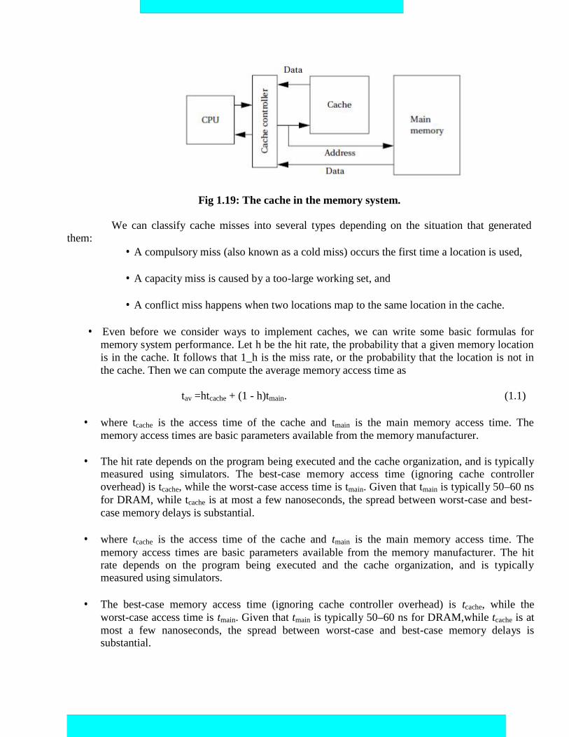
Fig 1.19: The cache in the memory system.
them:We can classify cache misses into several types depending on the situation that generated
A compulsory miss (also known as a cold miss) occurs the first time a location is used,
A capacity miss is caused by a too-large working set, and
A conflict miss happens when two locations map to the same location in the cache.
Even before we consider ways to implement caches, we can write some basic formulas formemory system performance. Let h be the hit rate, the probability that a given memory locationis in the cache. It follows that 1_h is the miss rate, or the probability that the location is not inthe cache. Then we can compute the average memory access time as
tav =htcache + (1 - h)tmain. (1.1)
where tcache is the access time of the cache and tmain is the main memory access time. Thememory access times are basic parameters available from the memory manufacturer.
The hit rate depends on the program being executed and the cache organization, and is typicallymeasured using simulators. The best-case memory access time (ignoring cache controlleroverhead) is tcache, while the worst-case access time is tmain. Given that tmain is typically 50–60 nsfor DRAM, while tcache is at most a few nanoseconds, the spread between worst-case and best-case memory delays is substantial.
where tcache is the access time of the cache and tmain is the main memory access time. Thememory access times are basic parameters available from the memory manufacturer. The hitrate depends on the program being executed and the cache organization, and is typicallymeasured using simulators.
The best-case memory access time (ignoring cache controller overhead) is tcache, while theworst-case access time is tmain. Given that tmain is typically 50–60 ns for DRAM,while tcache is atmost a few nanoseconds, the spread between worst-case and best-case memory delays issubstantial.

Modern CPUs may use multiple levels of cache as shown in Figure 1.20. The first-level cache(commonly known as L1 cache) is closest to the CPU, the second-level cache (L2 cache) feedsthe first-level cache, and so on.
The second-level cache is much larger but is also slower. If h1 is the first-level hit rate and h2 isthe rate at which access hit the second-level cache but not the first-level cache, then the averageaccess time for a two-level cache system is
tav = h1tL1 + h2tL2 +(1 - h1 - h2)tmain. ( 1.2)
o As the program’s working set changes, we expect locations to be removed fromthe cache to make way for new locations. When set-associative caches are used,we have to think about what happens when we throw out a value from the cacheto make room for a new value.
We do not have this problem in direct-mapped caches because every location maps onto aunique block, but in a set-associative cache we must decide which set will have itsblock thrown out to make way for the new block.
One possible replacement policy is least recently used (LRU), that is, throw out the blockthat has been used farthest in the past. We can add relatively small amounts of hardwareto the cache to keep track of the time since the last access for each block. Anotherpolicy is random replacement, which requires even less hardware to implement.
The simplest way to implement a cache is a direct-mapped cache, as shown in Figure1.20. The cache consists of cache blocks, each of which includes a tag to show whichmemory location is represented by this block, a data field holding the contents of thatmemory, and a valid tag to show whether the contents of this cache block are valid. Anaddress is divided into three sections.
The index is used to select which cache block to check. The tag is compared againstthe tag value in the block selected by the index. If the address tag matches the tagvalue in the block, that block includes the desired memorywwwlo.ancnaautniiovenrzi.ty.com
If the length of the data field is longer than the minimum addressable unit, then thelowest bits of the address are used as an offset to select the required value from thedata field. Given the structure of the cache, there is only one block that must bechecked to see whether a location is in the cache—the index uniquely determinesthat block. If the access is a hit, the data value is read from the cache.
Writes are slightly more complicated than reads because we have to update main memoryas well as the cache. There are several methods by which we can do this. The simplestscheme is known as write-through—every write changes both the cache and thecorresponding main memory location (usually through a write buffer).

This scheme ensures that the cache and main memory are consistent, but may generatesome additional main memory traffic. We can reduce the number of times we write tomain memory by using a write-back policy: If we write only when we remove a locationfrom the cache, we eliminate the writes when a location is written several times beforeit is removed from the cache.
The direct-mapped cache is both fast and relatively low cost, but it does have limits in its cachingpower due to its simple scheme for mapping the cache onto main memory. Consider a direct-mapped cache with four blocks, in which locations 0, 1, 2, and 3 all map to different blocks. Butlocations 4, 8, 12…all map to the same block as location 0; locations 1, 5, 9, 13…all map to asingle block; and so on. If two popular locations in a program happen to map onto the same block,we will not gain the full benefits of the cache. As seen in Section 5.6, this can create programperformance problems.
The limitations of the direct-mapped cache can be reduced by going to the set-associative cachestructure shown in Figure 1.21.A set-associative cache is characterized by the number of banks orways it uses, giving an n-way set-associative cache.
A set is formed by all the blocks (one for each bank) that share the same index. Each set isimplemented with a direct-mapped cache. A cache request is broadcast to all bankssimultaneously. If any of the sets has the location, the cache reports a hit.
Although memory locations map onto blocks using the same function, there are n separate blocksfor each set of locations. Therefore, we can simultaneously cache several locations that happen tomap onto the same cache block. The set associative cache structure incurs a little extra overheadand is slightly slower than a direct-mapped cache, but the higher hit rates that it can provide oftencompensate.
The set-associative cache generally provides higher hit rates than the direct mapped cachebecause conflicts between a small number of locations can be resolved within the cache. The set-associative cache is somewhat slower, so the CPU designer has to be careful that it doesn’t slowdown the CPU’s cycle time too much. A more important problem with set-associative caches forembedded program.
Design is predictability. Because the time penalty for a cache miss is so severe, we often wantto make sure that critical segments of our programs have good behavior in the cache. It isrelatively easy to determine when two memory locations will conflict in a direct-mapped cache.
Conflicts in a set-associative cache are more subtle, and so the behavior of a set-associativecache is more difficult to analyze for both humans and programs.
1.11 CPU PERFORMANCE:
Now that we have an understanding of the various types of instructions that CPUs can execute,we can move on to a topic particularly important in embedded computing: How fast can the CPUexecute instructions? In this section, we consider three factors that can substantially influence programperformance: pipelining and caching.
1.11.1 Pipelining
Modern CPUs are designed as pipelined machines in which several instructions are executed inparallel. Pipelining greatly increases the efficiency of the CPU. But like any pipeline, a CPU pipelineworks best when its contents flow smoothly.
Some sequences of instructions can disrupt the flow of information in the pipeline and,temporarily at least, slow down the operation of the CPU.

The ARM7 has a three-stage pipeline:
■ Fetch the instruction is fetched from memory.■ Decode the instruction’s opcode and operands are decoded to determine what function toperform.■ Execute the decoded instruction is executed.
Each of these operations requires one clock cycle for typical instructions. Thus, anormal instruction requires three clock cycles to completely execute, known as the latency ofinstruction execution. But since the pipeline has three stages, an instruction is completed inevery clock cycle. In other words, the pipeline has a throughput of one instruction per cycle.
Figure 1.22 illustrates the position of instructions in the pipeline during executionusing the notation introduced by Hennessy and Patterson [Hen06]. A vertical slice through thetimeline shows all instructions in the pipeline at that time. By following an instructionhorizontally, we can see the progress of its execution.
The C55x includes a seven-stage pipeline [Tex00B]:
1. Fetch.2. Decode.3. Address computes data and branch addresses.4. Access 1 reads data.5. Access 2 finishes data read.6. Read stage puts operands onto internal busses.7. Execute performs operations.
RISC machines are designed to keep the pipeline busy. CISC machines maydisplay a wide variation in instruction timing. Pipelined RISC machines typically have moreregular timing characteristics most instructions that do not have pipeline hazards display thesame latency.
1.11.2 Caching
We have already discussed caches functionally. Although caches are invisible in theprogramming model, they have a profound effect on performance. We introduce cachesbecause they substantially reduce memory access time when the requested location is in thecache.
However, the desired location is not always in the cache since it is considerablysmaller than main memory. As a result, caches cause the time required to access memory tovary considerably. The extra time required to access a memory location not in the cache isoften called the cache miss penalty.
The amount of variation depends on several factors in the system architecture, but a

cache miss is often several clock cycles slower than a cache hit. The time required toaccess a memory location depends on whether therequested location is in the cache. However, as we have seen, a location may not be in thecache for several reasons.
■ At a compulsory miss, the location has not been referenced before.
■ At a conflict miss, two particular memory locations are fighting for the same cache line.
■ At a capacity miss, the program’s working set is simply too large for the cache.
The contents of the cache can change considerably over the course of execution of a program.When we have several programs running concurrently on the CPU,
1.12 CPU POWER CONSUMPTION:
Power consumption is, in some situations, as important as execution time. In thissection we study the characteristics of CPUs that influence power consumption andmechanisms provided by CPUs to control how much power they consume. First, it isimportant to distinguish between energy and power. Power is, of course, energy consumptionper unit time. Heat generation depends on power consumption. Battery life, on the other hand,most directly depends on energy consumption. Generally, we will use the term power asshorthand for energy and power consumption, distinguishing between them only whennecessary.
The high-level power consumption characteristics of CPUs and other systemcomponents are derived from the circuits used to build those components. Today, virtually alldigital systems are built with complementary metal oxide semiconductor (CMOS) circuitry.The detailed circuit characteristics are best left to a study of VLSI design [Wol08], but thebasic sources of CMOS power consumption are easily identified and briefly described below.
■ Voltage drops: The dynamic power consumption of a CMOS circuit wiswwp.ranonpauonirvteirzoitny.acolmto thesquare of the power supply voltage (V2). Therefore, by reducing the power supply voltage tothe lowest level that provides the required performance, we can significantly reduce powerconsumption. We also may be able to add parallel hardware and even further reduce the powersupply voltage while maintaining required performance.
■ Toggling: A CMOS circuit uses most of its power when it is changing its output value. Thisprovides two ways to reduce power consumption. By reducing the speed at which the circuitoperates, we can reduce its power consumption (although not the total energy required for theoperation, since the result is available later).We can actually reduce energy consumption byeliminating unnecessary changes to the inputs of a CMOS circuit—eliminating unnecessaryglitches at the circuit outputs eliminates unnecessary power consumption.

UNIT IICOMPUTING PLATFORM AND DESIGN ANALYSIS
2.1 CPU BUSES:
A computer system encompasses much more than the CPU;it also includes memory and I/Odevices. The bus is the mechanism by which the CPU communicates with memory and devices. A busis, at a minimum, a collection of wires, but the bus also defines a protocol by which the CPU, memory,and devices communicate. One of the major roles of the bus is to provide an interface to memory. (Ofcourse, I/O devices also connect to the bus.)
2.1.1 Bus Protocols:
The basic building block of most bus protocols is the four-cycle handshake, illustrated inFigure 2.1. The handshake ensures that when two devices want to communicate, one is ready totransmit and the other is ready to receive.
The handshake uses a pair of wires dedicated to the handshake: enq (meaning enquiry) and ack(meaning acknowledge). Extra wires are used for the data transmitted during the handshake. The fourcycles are described below.
1. Device 1 raises its output to signal an enquiry, which tells device 2 that it should get ready to listenfor data.
2. When device 2 is ready to receive, it raises its output to signal an acknowledgment. At this point,devices 1 and 2 can transmit or receive.
3. Once the data transfer is complete, device 2 lowers its output, signaling that it has received the data.
4. After seeing that ack has been released, device 1 lowers its output.
At the end of the handshake, both handshaking signals are low, just as they were at the start of thehandshake. The system has thus returned to its original state in readiness for another handshake-enabled data transfer.
Microprocessor buses build on the handshake for communication between the CPU and othersystem components. The term bus is used in two ways.
The most basic use is as a set of related wires, such as address wires. However, the term may alsomean a protocol for communicating between components.
To avoid confusion, we will use the term bundle to refer to a set of related signals. Thefundamental bus operations are reading and writing. Figure 2.2 shows the structure of a typical bus thatsupports reads and writes.

The major components follow:
■ Clock provides synchronization to the bus components,
■ R/W is true when the bus is reading and false when the bus is writing,
■ Address is an a-bit bundle of signals that transmits the address for an access,
■ Data is an n-bit bundle of signals that can carry data to or from the CPU, and
■ Data ready signals when the values on the data bundle are valid.
2.1.2 DMA:
Standard bus transactions require the CPU to be in the middle of every read and writetransaction. However, there are certain types of data transfers iwnwww.anhniacunhivetrhziety.cComPU does not needto be involved.
For example, a high-speed I/O device may want to transfer a block of data into memory. Whileit is possible to write a program that alternately reads the device and writes to memory, it wouldbe faster to eliminate the CPU’s involvement and let the device and memory communicatedirectly. This capability requires that some unit other than the CPU be able to control operationson the bus.
Direct memory access (DMA) is a bus operation that allows reads and writes not controlled bythe CPU. A DMA transfer is controlled by a DMA controller, which requests control of the bus fromthe CPU.
After gaining control, the DMA controller performs read and write operations directly betweendevices and memory. Figure 2.3 shows the configuration of a bus with a DMA controller. The DMArequires the CPU to provide two additional bus signals:
■ The bus request is an input to the CPU through which DMA controllers askfor ownership of the bus.
■ The bus grant signals that the bus has been granted to the DMA controller.
A device that can initiate its own bus transfer is known as a bus master. Devices that do nothave the capability to be bus masters do not need to connect to a bus request and bus grant.
The DMA controller uses these two signals to gain control of the bus using a classic four-cyclehandshake. The bus request is asserted by the DMA controller when it wwwawn.antnsautnoivecrzoitny.tcrooml the bus, and thebus grant is asserted by the CPU when the bus is ready.
The CPU will finish all pending bus transactions before granting control of the bus to the DMAcontroller. When it does grant control, it stops driving the other bus signals: R/W, address, and so on.Upon becoming bus master, the DMA controller has control of all bus signals (except, of course, forbus request and bus grant).

2.2 MEMORY DEVICES:
There are several varieties of both read-only and read/write memories, each with its ownadvantages. After discussing some basic characteristics of memories, we describe RAMs and thenROMs.
4.2.1 Memory Device Organization
The most basic way to characterize a memory is by its capacity, such as 256 MB. However,manufacturers usually make several versions of a memory of a given size, each with a different datawidth. For example, a 256-MB memory may be available in two versions:
■ As a 64M *4-bit array, a single memory access obtains an 8-bit data item, with a maximum of 226
different addresses.
■ As a 32 M* 8-bit array, a single memory access obtains a 1-bit data item, with a maximum of 223
different addresses.
The height/width ratio of a memory is known as its aspect ratio. The best aspect ratio depends onthe amount of memory required. Internally, the data are stored in a two-dimensional array of memorycells as shown in Figure 2.4. Because the array is stored in two dimensions, the n-bit address receivedby the chip is split into a row and a column address (with n =r+ c).
The row and column select a particular memory cell. If the memory’s external width is 1 bit, thecolumn address selects a single bit; for wider data widths, the column address can be used to select asubset of the columns. Most memories include an enable signal that controls the tri-stating of data ontothe memory’s pins.
2.2.2 Random-Access Memories:
o Random-access memories can be both read and written. They are called random access because,unlike magnetic disks, addresses can be read in any order. Most bulk memory in modernsystems is dynamic RAM (DRAM). DRAM is very dense; it does, however, require that itsvalues be refreshed periodically since the values inside the memory cells decay over time.
o The dominant form of dynamic RAM today is the synchronous DRAMs (SDRAMs), whichuses clocks to improve DRAM performance. SDRAMs use Row Address Select (RAS) andColumn Address Select (CAS) signals to break the address into two parts, which select theproper row and column in the RAM array. Signal transitions are relative to the SDRAMclock,which allows the internal SDRAM operations to be pipelined.
As shown in Figure 2.5, transitions on the control signals are related to a clock [Mic00].RAS_ and CAS_ can therefore become valid at the same time.

o The address lines are not shown in full detail here; some address lines may not be activedepending on the mode in use. SDRAMs use a separate refresh signal to control refreshing.DRAM has to be refreshed roughly once per millisecond.
o Rather than refresh the entire memory at once, DRAMs refresh part of the memory at a time.When a section of memory is being refreshed, it cannot be accessed until the refresh iscomplete. The memory refresh occurs over fairly few seconds so that each section is refreshedevery few microseconds.
o SDRAMs include registers that control the mode in which the SDRAM operates. SDRAMssupport burst modes that allow several sequential addresses to be accessed by sending only oneaddress. SDRAMs generally also support an interleaved mode that exchanges pairs of bytes.
2.2.3 Read-Only Memories:
o Read-only memories (ROMs) are preprogrammed with fixed data. They are very useful inembedded systems since a great deal of the code, and perhaps some data, does not change overtime. Read-only memories are also less sensitive to radiation induced errors.
o There are several varieties of ROM available. The first-level distinction to be made is betweenfactory-programmed ROM (sometimes called mask-programmed ROM) and field-programmable ROM.
o Factory-programmed ROMs are ordered from the factory with particular programming. ROMscan typically be ordered in lots of a few thousand, but clearly factory programming is usefulonly when the ROMs are to be installed in some quantity.
o Field-programmable ROMs, on the other hand, can be programmed in the lab. Flash memory isthe dominant form of field-programmable ROM and is electrically erasable.
o Flash memory uses standard system voltage for erasing and programming, allowing it to bereprogrammed inside a typical system. This allows applications such as automatic distributionof upgrades—the flash memory can be reprogrammed while downloading the new memorycontents from a telephone line.
o Early flash memories had to be erased in their entirety; modern devices allow memory to beerased in blocks. Most flash memories today allow certain blocks to be protected.
o A common application is to keep the boot-up code in a protected block but allow updates toother memory blocks on the device. As a result, this form of flash is commonly known as boot-block flash.

2.3 I/O DEVICES:
Some of these devices are often found as on-chip devices in micro-controllers; others aregenerally implemented separately but are still commonly used. Looking at a few importantdevices now will help us understand both the requirements of device interfacing.
2.3.1 Timers and Counters:
Timers and counters are distinguished from one another largely by their use, not their logic.Both are built from adder logic with registers to hold the current value, with an increment inputthat adds one to the current register value.
However, a timer has its count connected to a periodic clock signal to measure time intervals,while a counter has its count input connected to an aperiodic signal in order to count the numberof occurrences of some external event. Because the same logic can be used for either purpose,the device is often called a counter/timer.
Figure 2.6 shows enough of the internals of a counter/timer to illustrate its operation. An n-bitcounter/timer uses an n-bit register to store the current state of the count and an array of halfsubtractors to decrement the count when the count signal is asserted.
Combinational logic checks when the count equals zero; the done output signals the zero count.It is often useful to be able to control the time-out, rather than require exactly 2n events tooccur. For this purpose, a reset register provides the value with which the count register is to beloaded.
The counter/timer provides logic to load the reset register. Most counters provide both cyclicand acyclic modes of operation. In the cyclic mode, once the counter reaches the done state, it isautomatically reloaded and the counting process continues. In acyclic mode, the counter/timerwaits for an explicit signal from the microprocessor to resume counting.
A watchdog timer is an I/O device that is used for internal operation of a system. As shown inFigure 2.7, the watchdog timer is connected into the CPU bus and also to the CPU’s reset line.
The CPU’s software is designed to periodically reset the watchdog timer, before the timer everreaches its time-out limit. If the watchdog timer ever does reach that limit, its time-out action isto reset the processor. In that case, the presumption is that either a software flaw or hardwareproblem has caused the CPU to misbehave. Rather than diagnose the problem, the system isreset to get it operational as quickly as possible.

2.3.2 A/D and D/A Converters
Analog/digital (A/D) and digital/analog (D/A) converters (typically known as ADCs andDACs, respectively) are often used to interface non digital devices to embedded systems.
The design of A/D and D/A converters themselves is beyond the scope of this book; weconcentrate instead on the interface to the microprocessor bus. Because A/D conversion requiresmore complex circuitry, it requires a somewhat more complex interface.
Analog/digital conversion requires sampling the analog input before converting it to digitalform. A control signal causes the A/D converter to take a sample and digitize it.
www.annauniverzity.com
There are several different types of A/D converter circuits, some of which take a constantamount of time, while the conversion time of others depends on the sampled value. Variable-time converters provide a done signal so that the microprocessor knows when the value is ready.
A typical A/D interface has, in addition to its analog inputs, two major digital inputs. A dataport allows A/D registers to be read and written, and a clock input tells when to start the nextconversion.
D/A conversion is relatively simple, so the D/A converter interface generally includes only thedata value. The input value is continuously converted to analog form.
2.3.3 LEDs
Light-emitting diodes (LEDs) are often used as simple displays by themselves, and arrays ofLEDs may form the basis of more complex displays. Figure 2.8 shows how to connect an LEDto a digital output.
A resistor is connected between the output pin and the LED to absorb the voltage differencebetween the digital output voltage and the 0.7 V drop across the LED. When the digital outputgoes to 0, the LED voltage is in the devices off region and the LED is not on.
2.3.4 Displays
A display device may be either directly driven or driven from a frame buffer. Typically,displays with a small number of elements are driven directly by logic, while large displays use aRAM frame buffer.
The n-digit array, shown in Figure 2.9, is a simple example of a display that is usually directlydriven. A single-digit display typically consists of seven segments; each segment may be eitheran LED or a liquid crystal display (LCD) element.
Display relies on the digits being visible for some time after the drive to the digit is removed,which is true for both LEDs and LCDs.
The digit input is used to choose which digit is currently being updated, and the selected digitactivates its display elements based on the current data value.

The display’s driver is responsible for repeatedly scanning through the digits and presenting thecurrent value of each to the display.
A frame buffer is a RAM that is attached to the system bus. The microprocessor writes valuesinto the frame buffer in whatever order is desired.
The pixels in the frame buffer are generally written to the display in raster order (by tradition,the screen is in the fourth quadrant) by reading pixels sequentially.
Many large displays are built using LCD. Each pixel in the display is formed by a single liquidcrystal.
Early LCD panels were called passive matrix because they relied on a two-dimensional grid ofwires to address the pixels. Modern LCD panels use an active matrix system that puts atransistor at each pixel to control access to the LCD. Active matrix displays provide highercontrast and a higher-quality display.
2.3.5 Touchscreens
A touchscreen is an input device overlaid on an output device. The touchscreen registers theposition of a touch to its surface. By overlaying this on a display, the user can react toinformation shown on the display.
The two most common types of touchscreens are resistive and capacitive. A resistivetouchscreen uses a two-dimensional voltmeter to sense position. As shown in Figure 2.10, thetouchscreen consists of two conductive sheets separated by spacer balls. The top conductivesheet is flexible so that it can be pressed to touch the bottom sheet.
A voltage is applied across the sheet; its resistance causes a voltage gradient to appear acrossthe sheet. The top sheet samples the conductive sheet’s applied voltage at the contact point. Ananalog/digital converter is used to measure the voltage and resulting position.
The touchscreen alternates between x and y position sensing by alternately applying horizontaland vertical voltage gradients.information shown on the display.
The two most common types of touchscreens are resistive and capacitive. A resistivetouchscreen uses a two-dimensional voltmeter to sense position. As shown in Figure 2.10, thetouchscreen consists of two conductive sheets separated by spacer balls. The top conductivesheet is flexible so that it can be pressed to touch the bottom sheet.
A voltage is applied across the sheet; its resistance causes a voltage gradient to appear acrossthe sheet. The top sheet samples the conductive sheet’s applied voltage at the contact point. Ananalog/digital converter is used to measure the voltage and resulting position.
The touchscreen alternates between x and y position sensing by alternately applying horizontaland vertical voltage gradients.
2.4 COMPONENT INTERFACING:
Building the logic to interface a device to a bus is not too difficult but does take some attention todetail. We first consider interfacing memory components to the bus, since that is relatively simple, andthen use those concepts to interface to other types of devices.
2.4.1 Memory Interfacing

If we can buy a memory of the exact size we need, then the memory structure is simple. If weneed more memory than we can buy in a single chip, then we must construct the memory out of severalchips. We may also want to build a memory that is wider than we can buy on a single chip; forexample, we cannot generally buy a 32-bit-wide memory chip. We canwwewa.asninlayunicveorznitsy.tcroumct a memory of agiven width (32 bits, 64 bits, etc.) by placing RAMs in parallel.
We also need logic to turn the bus signals into the appropriate memory signals. For example, mostbusses won’t send address signals in row and column form. We also need to generate the appropriaterefresh signals.
2.4.2 Device Interfacing
Some I/O devices are designed to interface directly to a particular bus, forming gluelessinterfaces. But glue logic is required when a device is connected to a bus for which it is not designed.
An I/O device typically requires a much smaller range of addresses than a memory, soaddresses must be decoded much more finely. Some additional logic is required to cause the bus to readand write the device’s registers.
2.5 DESIGN WITH MICROPROCESSORS:
2.5.1 System Architecture
We know that an architecture is a set of elements and the relationships between them that togetherform a single unit. The architecture of an embedded computing system is the blueprint forimplementing that system—it tells you what components you need and how you put them together.
The architecture of an embedded computing system includes both hardware and software elements.Let’s consider each in turn.
The hardware architecture of an embedded computing system is the more obvious manifestation ofthe architecture since you can touch it and feel it. It includes several elements, some of which maybe less obvious than others.
o CPU An embedded computing system clearly contains a microprocessor. But which one? Thereare many different architectures, and even within an architecture we can select between modelsthat vary in clock speed, bus data width, integrated peripherals, and so on. The choice of theCPU is one of the most important, but it cannot be made without considering the software thatwill execute on the machine.
o Bus The choice of a bus is closely tied to that of a CPU, since the bus is an integral part of themicroprocessor. But in applications that make intensive use of the bus due to I/O or other datatraffic, the bus may be more of a limiting factor than the CPU. Attention must be paid to therequired data bandwidths to be sure that the bus can handle the traffic.
o Memory Once again, the question is not whether the system will have memory but thecharacteristics of that memory. The most obvious characteristic is total size, which depends onboth the required data volume and the size of the program instructions. The ratio of ROM toRAM and selection of DRAM versus SRAM can have a significant influence on the cost of thesystem. The speed of the memory will play a large part in determwwiwn.ianngaunsiyvesrztietym.comperformance.

o Input and output devices The user’s view of the input and output mechanisms may notcorrespond to the devices connected to the microprocessor. For example, a set of switches andknobs on a front panel may all be controlled by a single microcontroller, which is in turnconnected to the main CPU.
For a given function, there may be several different devices of varying sophistication and cost thatcan do the job. The difficulty of using a particular device, such as the amount of glue logic requiredto interface it, may also play a role in final device selection.
2.5.2 Hardware Design
The design complexity of the hardware platform can vary greatly, from a totally off-the-shelfsolution to a highly customized design.
At the board level, the first step is to consider evaluation boards supplied by the microprocessormanufacturer or another company working in collaboration with the manufacturer. Evaluation boardsare sold for many microprocessor systems; they typically include the CPU, some memory, a serial linkfor downloading programs, and some minimal number of I/O devices. Figure 2.11 shows an ARMevaluation board manufactured by Sharp.
The evaluation board may be a complete solution or provide what you need with only slightmodifications. If the evaluation board is supplied by the microprocessor vendor, its design (netlist,board layout, etc.) may be available from the vendor; companies provide such information to make iteasy for customers to use their microprocessors. If the evaluation board comes from a third party, itmay be possible to contract them to design a new board with your required modifications, or you canstart from scratch on a new board design.
The other major task is the choice of memory and peripheral components. In the case of I/Odevices, there are two alternatives for each device: selecting a component from a catalog or designingone yourself. When shopping for devices from a catalog, it is important to read data sheets carefully itmay not be trivial to figure out whether the device does what you need it to do.
2.6 DEVELOPMENT AND DEBUGGING:
2.6.1 Development Environments
A typical embedded computing system has a relatively small amount of everything, includingCPU horsepower, memory, I/O devices, and so forth. As a result, it is common to do at least part of thesoftware development on a PC or workstation known as a host as illustrated in Figure 2.12. Thehardware on which the code will finally run is known as the target. The host and target are frequentlyconnected by a USB link, but a higher-speed link such as Ethernet can also be used.
The target must include a small amount of software to talk to the host system. That software willtake up some memory, interrupt vectors, and so on, but it should generally leave the smallest possiblefootprint in the target to avoid interfering with the application software.
The host should be able to do the following:

■ load programs into the target,
■ start and stop program execution on the target, and
■ examine memory and CPU registers.
2.6.2 Debugging Techniques: A good deal of software debugging can be done by compiling and executing the code on a PC or
workstation. But at some point it inevitably becomes necessary to run code on the embeddedhardware platform.
Embedded systems are usually less friendly programming environments than PCs. Nonetheless,the resourceful designer has several options available for debugging the system.
The serial port found on most evaluation boards is one of the most important debugging tools. Infact, it is often a good idea to design a serial port into an embedded system even if it will not beused in the final product; the serial port can be used not only for development debugging but alsofor diagnosing problems in the field.
Another very important debugging tool is the breakpoint. The simplest form of a breakpoint is forthe user to specify an address at which the program’s execution is to break. When the PC reachesthat address, control is returned to the monitor program. From the monitor program, the user canexamine and/or modify CPU registers, after which execution can be continued. Implementingbreakpoints does not require using exceptions or external devices.
2.6.3 Debugging Challenges
Logical errors in software can be hard to track down, but errors in real-time code can createproblems that are even harder to diagnose. Real-time programs are required to finish their workwithin a certain amount of time; if they run too long, they can create very unexpected behavior.
The exact results of missing real-time deadlines depend on the detailed characteristics of the I/Odevices and the nature of the timing violation. This makes debugging real-time problemsespecially difficult.
Unfortunately, the best advice is that if a system exhibits truly unusual behavior, misseddeadlines should be suspected. In-circuit emulators, logic analyzers, and even LEDs can beuseful tools in checking the execution time of real-time code to determine whether it in factmeets its deadline.
2.7 PROGRAM DESIGN:
2.7.1 Components for Embedded Programs:
In this section, we consider code for three structures or components that are commonly used inembedded software: the state machine, the circular buffer, and the queue. State machines are well
www.annauniverzity.comsuited to reactive systems such as user interfaces; circular buffers and queues are useful in digital signalprocessing.
2.7.1.1 State Machines
When inputs appear intermittently rather than as periodic samples, it is often convenient to think

of the system as reacting to those inputs.
The reaction of most systems can be characterized in terms of the input received and the currentstate of the system. This leads naturally to a finite-state machine style of describing the reactivesystem’s behavior.
Moreover, if the behavior is specified in that way, it is natural to write the programimplementing that behavior in a state machine style.
The state machine style of programming is also an efficient implementation of suchcomputations. Finite-state machines are usually first encountered in the context of hardwaredesign.
2.7.2 Stream-Oriented Programming and Circular Buffers
The data stream style makes sense for data that comes in regularly and must be processed onthe fly. For each sample, the filter must emit one output that depends on the values of the last n inputs.In a typical workstation application, we would process the samples over a given interval by readingthem all in from a file and then computing the results all at once in a batch process. In an embeddedsystem we must not only emit outputs in real time, but we must also do so using a minimum amount ofmemory.
The circular buffer is a data structure that lets us handle streaming data in an efficient way.Figure 2.13 illustrates how a circular buffer stores a subset of the data stream. At each point in time, thealgorithm needs a subset of the data stream that forms a window into the stream. The window slideswith time as we throw out old values no longer needed and add new values. Since the size of thewindow does not change, we can use a fixed-size buffer to hold the current data.
To avoid constantly copying data within the buffer, we will move the head of the buffer intime. The buffer points to the location at which the next sample will be placed; every time we add asample, we automatically overwrite the oldest sample, which is the one that needs to be thrown out.When the pointer gets to the end of the buffer, it wraps around to the top.
2.8 MODELS OF PROGRAMS:
Data Flow Graphs:
A data flow graph is a model of a program with no conditionals. In a high-level programminglanguage, a code segment with no conditionals—more precisely, with only one entry and exit point isknown as a basic block. Figure 2.14 shows a simple basic block. As the C code is executed, we wouldenter this basic block at the beginning and execute all the statements.
w = a+b;x = a-c;y = x+d;x = a+c;z = y+e;
Fig 2.14 A basic block in C.
w = a+b;x = a-c;

y = x1+d;x2= a+c;z = y+e;
Fig 2.14 The basic block in single-assignment form.
Before we are able to draw the data flow graph for this code we need to modify it slightly.There are two assignments to the variable x—it appears twice on the left side of an assignment. Weneed to rewrite the code in single-assignment form, in which a variable appears only once on the leftside.
Since our specification is C code, we assume that the statements are executed sequentially, sothat any use of a variable refers to its latest assigned value. In this case, x is not reused in this block(presumably it is used elsewhere), so we just have to eliminate the multiple assignment to x. The resultis shown in Figure 2.14, where we have used the names x1 and x2 to distinguish the separate uses of x.
The single-assignment form is important because it allows us towwidwe.annaiufnyivearziutyn.cioqmue location in thecode where each named location is computed. As an introduction to the data flow graph, we use twotypes of nodes in the graph round nodes denote operators and square nodes represent values.
The value nodes may be either inputs to the basic block, such as a and b, or variables assignedto within the block, such as w and x1.
The data flow graph for our single-assignment code is shown in Figure 2.15.The single-assignment form means that the data flow graph is acyclic—if we assigned to x multiple times, then thesecond assignment would form a cycle in the graph including x and the operators used to compute x.
2.9 ASSEMBLY AND LINKING :
Assembly and linking are the last steps in the compilation process they turn a list ofinstructions into an image of the program’s bits in memory. Loading actually puts the program inmemory so that it can be executed. In this section, we survey the basic techniques required forassembly linking to help us understand the complete compilation and loading process.
Figure 2.16 highlights the role of assemblers and linkers in the compilation process. Thisprocess is often hidden from us by compilation commands that do everything required to generate anexecutable program. As the figure shows, most compilers do not directly generate machine code, butinstead create the instruction-level program in the form of human-readable assembly language.Generating assembly language rather than binary instructions frees the compiler writer from detailsextraneous to the compilation process, which includes the instruction format as well as the exactaddresses of instructions and data.
The assembler’s job is to translate symbolic assembly language statements into bit-levelrepresentations of instructions known as object code. The assembler takes care of instruction formatsand does part of the job of translating labels into addresses. However, since the program may be builtfrom many files, the final steps in determining the addresses of instructions and data are performed bythe linker, which produces an executable binary file. That file may not necessarily be located in theCPU’s memory, however, unless the linker happens to create the executable directly in RAM. Theprogram that brings the program into memory for execution is called a loader.
The simplest form of the assembler assumes that the starting address of the assemblylanguage program has been specified by the programmer. The addresses in such a program are knownas absolute addresses.

2.9.1 Assemblers
When translating assembly code into object code, the assembler must translate opcodes andformat the bits in each instruction, and translate labels into addresses. In this section, we review thetranslation of assembly language into binary. Labels make the assembly process more complex, butthey are the most important abstraction provided by the assembler. Labels let the programmer (a humanprogrammer or a compiler generating assembly code) avoid worrying about the locations ofinstructions and data. Label processing requires making two passes through the assembly source codeas follows:
1. The first pass scans the code to determine the address of each label.
2. The second pass assembles the instructions using the label values computed in the first pass.
As shown in Figure 2.17, the name of each symbol and its address is stored in a symbol tablethat is built during the first pass. The symbol table is built by scanningwwfwro.anmnautnhiverzfitiyr.csotminstruction to thelast.
During scanning, the current location in memory is kept in a program location counter (PLC).Despite the similarity in name to a program counter, the PLC is not used to execute the program, onlyto assign memory locations to labels. For example, the PLC always makes exactly one pass through theprogram, whereas the program counter makes many passes over code in a loop. Thus, at the start of thefirst pass, the PLC is set to the program’s starting address and the assembler looks at the first line. Afterexamining the line, the assembler updates the PLC to the next location (since ARM instructions arefour bytes long, the PLC would be incremented by four) and looks at the next instruction. If theinstruction begins with a label, a new entry is made in the symbol table, which includes the label nameand its value. The value of the label is equal to the current value of the PLC. At the end of the first pass,the assembler rewinds to the beginning of the assembly language file to make the second pass. Duringthe second pass, when a label name is found, the label is looked up in the symbol table and its valuesubstituted into the appropriate place in the instruction.
Fig 2.17 Symbol table processing during assembly.
But how do we know the starting value of the PLC? The simplest case is absolute addressing.In this case, one of the first statements in the assembly language program is a pseudo-op that specifiesthe origin of the program, that is, the location of the first address in the program. A common name forthis pseudo-op (e.g., the one used for the ARM) is the ORG statement.
ORG 2000
Which puts the start of the program at location 2000. This pseudo-op accomplishes this bysetting the PLC’s value to its argument’s value, 2000 in this case. Assemblers generally allow aprogram to have many ORG statements in case instructions or data must be spread around various spotsin memory.
2.9.2 Linking:

Many assembly language programs are written as several smaller pieces rather than as a single largefile. Breaking a large program into smaller files helps delineate program modularity. If the programuses library routines, those will already be preassembled, and assembly language source code forthe libraries may not be available for purchase.
A linker allows a program to be stitched together out of several smaller pieces. The linker operateson the object files created by the assembler and modifies the assembled code to make the necessarylinks between files.
Some labels will be both defined and used in the same file. Other wlawbwe.alnsnauwniivlelrzibtye.codmefined in a singlefile but used elsewhere as illustrated in Figure 2.18. The place in the file where a label is defined isknown as an entry point. The place in the file where the label is used is called an externalreference.
The main job of the loader is to resolve external references based on available entry points. As aresult of the need to know how definitions and references connect, the assembler passes to thelinker not only the object file but also the symbol table.
Even if the entire symbol table is not kept for later debugging purposes, it must at least pass theentry points. External references are identified in the object code by their relative symbolidentifiers.
The linker proceeds in two phases.
o First, it determines the address of the start of each object file. The order in which object files areto be loaded is given by the user, either by specifying parameters when the loader is run or bycreating a load map file that gives the order in which files are to be placed in memory. Giventhe order in which files are to be placed in memory and the length of each object file, it is easyto compute the starting address of each file.
o At the start of the second phase, the loader merges all symbol tables from the object files into asingle, large table. It then edits the object files to change relative addresses into addresses. Thisis typically performed by having the assembler write extra bits into the object file to identify theinstructions and fields that refer to labels. If a label cannot be found in the merged symbol table,it is undefined and an error message is sent to the user.
2.10 BASIC COMPILATION TECHNIQUES:
It is useful to understand how a high-level language program is translated into instructions.Since implementing an embedded computing system often requires controlling the instructionsequences used to handle interrupts, placement of data and instructions in memory, and so forth,understanding how the compiler works can help you know when you cannot rely on the compiler.
Next, because many applications are also performance sensitive, understanding how code isgenerated can help you meet your performance goals, either by writing high-level code that getscompiled into the instructions you want or by recognizing when you must write your own assemblycode.

The compilation process is summarized in Figure 2.19. Compilation begins with high-levellanguage code such as C and generally produces assembly code. (Directly producing object codesimply duplicates the functions of an assembler which is a very desirable stand-alone program to have.)
The high-level language program is parsed to break it into statements and expressions. Inaddition, a symbol table is generated, which includes all the named objects in the program. Somecompilers may then perform higher-level optimizations that can be viewed as modifying the high-levellanguage program input without reference to instructions.
Simplifying arithmetic expressions is one example of a machine-independent optimization.Not all compilers do such optimizations, and compilers can vary widely regarding which combinationsof machine-independent optimizations they do perform.
Instruction-level optimizations are aimed at generating code. They may work directly on realinstructions or on a pseudo-instruction format that is later mapped onto the instructions of the targetCPU. This level of optimization also helps modularize the compiler by allowing code generation tocreate simpler code that is later optimized. For example, consider the following array access code:
x[i] = c*x[i];A simple code generator would generate the address for x[i] twice, once for each
appearance in the statement. The later optimization phases can recognize this as an example ofcommon expressions that need not be duplicated. While in this simple case it would bepossible to create a code generator that never generated the redundant expression, taking intoaccount every such optimization at code generation time is very difficult. We get better codeand more reliable compilers by generating simple code first and then optimizing it.

2.11 ANALYSIS AND OPTIMIZATION OF EXCUTION TIME, POWER, NRGY , PROGRAMSIZE:
The memory footprint of a program is determined by the size of its data and instructions. Bothmust be considered to minimize program size.
Data provide an excellent opportunity for minimizing size because the data are most highlydependent on programming style. Because inefficient programs often keep several copies ofdata, identifying and eliminating duplications can lead to significant memory savings usuallywith little performance penalty.
Buffers should be sized carefully rather than defining a data array to a large size that theprogram will never attain, determine the actual maximum amount of data held in the bufferand allocate the array accordingly. Data can sometimes be packed, such as by storing severalflags in a single word and extracting them by using bit-level operations.
A very low-level technique for minimizing data is to reuse values. For instance, if severalconstants happen to have the same value, they can be mapped to the same location. Databuffers can often be reused at several different points in the program. This technique must beused with extreme caution, however, since subsequent versions of the program may not usethe same values for the constants.
A more generally applicable technique is to generate data on the fly rather than store it. Ofcourse, the code required to generate the data takes up space in the program, but whencomplex data structures are involved there may be some net space savings from using code togenerate data.
Minimizing the size of the instruction text of a program requires a mix of high-level programtransformations and careful instruction selection.
Encapsulating functions in subroutines can reduce program size when done carefully. Becausesubroutines have overhead for parameter passing that is not obvious from the high-levellanguage code, there is a minimum-size function body for which a subroutine makes sense.
Architectures that have variable-size instruction lengths are wpwawr.taincnauulnaivrelrzyityg.comod candidates forcareful coding to minimize program size, which may require assembly language coding of keyprogram segments. There may also be cases in which one or a sequence of instructions ismuch smaller than alternative implementations for example, a multiply-accumulate instructionmay be both smaller and faster than separate arithmetic operations.
When reducing the number of instructions in a program, one important technique is the properuse of subroutines. If the program performs identical operations repeatedly, these operationsare natural candidates for subroutines.
Even if the operations vary somewhat, you may be able to construct a properly parameterizedsubroutine that saves space. Of course, when considering the code size savings, the subroutine

linkage code must be counted into the equation. There is extra code not only in the subroutinebody but also in each call to the subroutine that handles parameters.. In some cases, properinstruction selection may reduce code size; this is particularly true in CPUs that use variable-length instructions
Some microprocessor architectures support dense instruction sets, specially designedinstruction sets that use shorter instruction formats to encode the instructions.
The ARM Thumb instruction set and the MIPS-16 instruction set for the MIPS architectureare two examples of this type of instruction set. In many cases, a microprocessor that supportsthe dense instruction set also supports the normal instruction set, although it is possible tobuild a microprocessor that executes only the dense instruction set.
Special compilation modes produce the program in terms of the dense instruction set. Programsize of course varies with the type of program, but programs using the dense instruction setare often 70 to 80% of the size of the standard instruction set equivalents.
2.12 PROGRAM VALIDATION AND TESTING :
Complex systems need testing to ensure that they work as they are intended. But bugs can besubtle, particularly in embedded systems, where specialized hardware and real-time responsivenessmake programming more challenging. Fortunately, there are many available techniques for softwaretesting that can help us generate a comprehensive set of tests to ensure that our system works properly.
The first question we must ask ourselves is how much testing is enough. Clearly, we cannot testthe program for every possible combination of inputs. Because we cannot implement an infinitenumber of tests, we naturally ask ourselves what a reasonable standard of thoroughness is. One of themajor contributions of software testing is to provide us with standards of thoroughness that make sense.Following these standards does not guarantee that we will find all bugs.
The two major types of testing strategies:
■ Black-box methods generate tests without looking at the internal structure of the program.
■ Clear-box (also known as white-box) methods generate tests based on the program structure.
2.12.1 Clear-Box Testing:
The control/data flow graph extracted from a program’s source code is an important tool indeveloping clear-box tests for the program. To adequately test the program, we must exercise both itscontrol and data operations.
In order to execute and evaluate these tests, we must be able to control variables in theprogram and observe the results of computations, much as in manufacturing testing. In general, we mayneed to modify the program to make it more testable. By adding new inputs and outputs, we can usuallysubstantially reduce the effort required to find and execute the test.

No matter what we are testing, we must accomplish the following three things in a test:
■ Provide the program with inputs that exercise the test we are interested in.
■ Execute the program to perform the test.
■ Examine the outputs to determine whether the test was successful.
2.12.2 Black-Box Testing:
Black-box tests are generated without knowledge of the code being tested. When usedalone, black-box tests have a low probability of finding all the bugs in a program. Butwhen used in conjunction with clear-box tests they help provide a well-rounded test set, sinceblack-box tests are likely to uncover errors that are unlikely to be found by tests extracted fromthe code structure.
Black-box tests can really work. For instance, when asked to test an instrument whosefront panel was run by a microcontroller, one acquaintance of the author used his hand todepress all the buttons simultaneously. The front panel immediately locked up. This situationcould occur in practice if the instrument were placed face-down on a table, but discovery ofthis bug would be very unlikely via clear-box tests.
One important technique is to take tests directly from the specification for the codeunder design. The specification should state which outputs are expected for certain inputs.Tests should be created that provide specified outputs and evaluate whether the results alsosatisfy the inputs.
We can’t test every possible input combination, but some rules of thumb helpus select reasonable sets of inputs. When an input can range across a set of values, it is a verygood idea to test at the ends of the range. For example, if an input must be between 1 and 10, 0,1, 10, and 11 are all important values to test. We should be sure to consider tests both withinand outside the range, such as, testing values within the range and outside the range. We maywant to consider tests well outside the valid range as well as boundary-condition tests.
Random tests form one category of black-box test. Random values are generatedwith a given distribution. The expected values are computed independently of the system,and then the test inputs are applied. A large number of tests must be applied for the results tobe statistically significant, but the tests are easy to generate. Another scenario is to test certaintypes of dwawtwa.avnnaauluniveesrz.ityF.coomr example, integer valued inputs can be generated at interesting valuessuch as 0, 1, and values near the maximum end of the data range. Illegal values can be tested aswell.
Regression tests form an extremely important category of tests. When tests arecreated during earlier stages in the system design or for previous versions of the system, thosetests should be saved to apply to the later versions of the system. Clearly, unless the system

specification changed, the new system should be able to pass old tests. In some cases old bugscan creep back into systems, such as when an old version of a software module isinadvertently installed. In other cases regression tests simply exercise the code in differentways than would be done for the current version of the code and therefore possibly exercisedifferent bugs.

UNIT IIIPROCESS AND OPERATING SYSTEMS
3.1 MULTIPLE TASKS AND MULTIPLE PROCESSES:
3.1.1 Tasks and Processes
Many (if not most) embedded computing systems do more than one thing that is, theenvironment can cause mode changes that in turn cause the embedded system to behave quitedifferently. For example, when designing a telephone answering machine,
We can define recording a phone call and operating the user’s control panel as distinct tasks,because they perform logically distinct operations and they must be performed at very differentrates. These different tasks are part of the system’s functionality, but that application-levelorganization of functionality is often reflected in the structure of the program as well.
A process is a single execution of a program. If we run the same program two different times,we have created two different processes. Each process has its own state that includes not onlyits registers but all of its memory. In some OSs, the memory management unit is used to keepeach process in a separate address space. In others, particularly lightweight RTOSs, theprocesses run in the same address space. Processes that share the same address space are oftencalled threads.
As shown in Figure 3.1, this device is connected to serial ports on both ends. The input to thebox is an uncompressed stream of bytes. The box emits a compressed string of bits on theoutput serial line, based on a predefined compression table. Such a box may be used, forexample, to compress data being sent to a modem.
The program’s need to receive and send data at different rates for example, the program mayemit 2 bits for the first byte and then 7 bits for the secondwwbwy.atnenauwnivielrlzitoy.bcovmiously find itselfreflected in the structure of the code. It is easy to create irregular, ungainly code to solve thisproblem; a more elegant solution is to create a queue of output bits, with those bits beingremoved from the queue and sent to the serial port in 8-bit sets.
But beyond the need to create a clean data structure that simplifies the control structure of thecode, we must also ensure that we process the inputs and outputs at the proper rates. Forexample, if we spend too much time in packaging and emitting output characters, we may dropan input character. Solving timing problems is a more challenging problem.
The text compression box provides a simple example of rate control problems. A control panelon a machine provides an example of a different type of rate control problem, the asynchronousinput.
The control panel of the compression box may, for example, include a compression modebutton that disables or enables compression, so that the input text is passed through unchangedwhen compression is disabled. We certainly do not know when the user will push thecompression mode button the button may be depressed asynchronously relative to the arrival ofcharacters for compression.

3.1.2 Multirate Systems
Implementing code that satisfies timing requirements is even more complex when multiplerates of computation must be handled. Multirate embedded computing systems are very common,including automobile engines, printers, and cell phones. In all these systems, certain operations must beexecuted periodically, and each operation is executed at its own rate.
3.1.3 Timing Requirements on Processes
o Processes can have several different types of timing requirements imposed on them by theapplication. The timing requirements on a set of processes strongly influence the type ofscheduling that is appropriate. A scheduling policy must define the timing requirements that ituses to determine whether a schedule is valid. Before studying scheduling proper, we outline thetypes of process timing requirements that are useful in embedded system design.
o Figure 3.2 illustrates different ways in which we can define two important requirements onprocesses: release time and deadline.
o The release time is the time at which the process becomes ready to execute; this is not necessarilythe time at which it actually takes control of the CPU and starts to run. An aperiodic process is bydefinition initiated by an event, such as external data arriving or data computed by anotherprocess.
o The release time is generally measured from that event, although the system may want to makethe process ready at some interval after the event itself. For a periodically executed process, thereare two common possibilities.
o In simpler systems, the process may become ready at the beginning of the period. Moresophisticated systems, such as those with data dependencies between processes, may set therelease time at the arrival time of certain data, at a time after the start of the period.
o A deadline specifies when a computation must be finished. The deadline for an aperiodic processis generally measured from the release time, since that is the only reasonable time reference. Thedeadline for a periodic process may in general occur at some time other than the end of the period.
o Rate requirements are also fairly common. A rate requirement wspwwe.caninfaiuensivehrzoityw.comquickly processesmust be initiated.
o The period of a process is the time between successive executions. For example, the period of adigital filter is defined by the time interval between successive input samples.
o The process’s rate is the inverse of its period. In a multirate system, each process executes at itsown distinct rate.

o The most common case for periodic processes is for the initiation interval to be equal to theperiod. However, pipelined execution of processes allows the initiation interval to be less than theperiod. Figure 3.3 illustrates process execution in a system with four CPUs.
3.1.4 CPU Metrics
We also need some terminology to describe how the process actually executes. The initiationtime is the time at which a process actually starts executing on the CPU. The completion time is thetime at which the process finishes its work.
The most basic measure of work is the amount of CPU time expended by a process. The CPUtime of process i is called Ci . Note that the CPU time is not equal to the completion time minusinitiation time; several other processes may interrupt execution. The total CPU time consumed by a setof processes is
T= ∑ Ti (3.1)
We need a basic measure of the efficiency with which we use the CPU. The simplest andmost direct measure is utilization:
U=CPU time for useful work/total available CPU time (3.2)
Utilization is the ratio of the CPU time that is being used for useful computations to the totalavailable CPU time. This ratio ranges between 0 and 1, with 1 meaning that all of the available CPUtime is being used for system purposes. The utilization is often expressed as a percentage. If wemeasure the total execution time of all processes over an interval of time t, then the CPU utilization is
U=T/t. (3.3)
3.2 PROCESSES AND CONTEXT SWITCHING:
The best way to understand processes and context is to dive into an RTOS implementation. Wewill use the FreeRTOS.org kernel as an example; in particular, we will use version 4.7.0 for the ARM7AT91 platform. A process is known in FreeRTOS.org as a task. Task priorities in FreeRTOS.org areranked opposite to the convention we use in the rest of the book: higher numbers denote higherpriorities and the priority 0 task is the idle task.
To understand the basics of a context switch, let’s assume that the set of tasks is in steady state:Everything has been initialized, the OS is running, and we are ready for a timer interrupt. Figure 3.4shows a sequence diagram for a context switch in freeRTOS.org. This diagram shows the applicationtasks, the hardware timer, and all the functions in the kernel that are involved in the context switch:
■ vPreemptiveTick () is called when the timer ticks.
■ portSAVE_CONTEXT() swaps out the current task context..
■ vTaskSwitchContext ( ) chooses a new task.
■ portRESTORE_CONTEXT() swaps in the new context.
3.3 OPERATING SYSTEMS:
An Operating system is a program that controls the execution of application programs and acts as an

interface between the user of a computer and the computer hardware.
A more common definition is that the operating system is the one program running at all times onthe computer (usually called the kernel), with all else being applications programs.
An Operating system is concerned with the allocation of resources and services, such as memory,processors, devices and information. The Operating System correspondingly includes programs tomanage these resources, such as a traffic controller, a scheduler, memory management module, I/Oprograms, and a file system.
3.4 SCHDULING POLICIES:
A scheduling policy defines how processes are selected for promotion from the ready state to therunning state. Every multitasking OS implements some type of scheduling policy. Choosing the rightscheduling policy not only ensures that the system will meet all its timing requirements, but it alsohas a profound influence on the CPU horsepower required to implement the system’s functionality.
Schedulability means whether there exists a schedule of execution for the processes in a system thatsatisfies all their timing requirements. In general, we must wcwown.santnrauuncitverzaity.csomchedule to show

schedulability, but in some cases we can eliminate some sets of processes as unschedulable usingsome very simple tests.
Utilization is one of the key metrics in evaluating a scheduling policy. Our most basic requirement isthat CPU utilization be no more than 100% since we can’t use the CPU more than 100% of the time.
When we evaluate the utilization of the CPU, we generally do so over a finite period that covers allpossible combinations of process executions. For periodic processes, the length of time that must beconsidered is the hyperperiod, which is the least-common multiple of the periods of all theprocesses. (The complete schedule for the least-common multiple of the periods is sometimes calledthe unrolled schedule.) If we evaluate the hyperperiod, we are sure to have considered all possiblecombinations of the periodic processes.
We will see that some types of timing requirements for a set of processes imply that we cannotutilize 100% of the CPU’s execution time on useful work, even ignoring context switching overhead.However, some scheduling policies can deliver higher CPU utilizations than others, even for thesame timing requirements.
One very simple scheduling policy is known as cyclostatic scheduling or sometimes as TimeDivision Multiple Access scheduling. As illustrated in Figure 3.5, a cyclostatic schedule is dividedinto equal-sized time slots over an interval equal to the length of the hyperperiod H. Processesalways run in the same time slot.
o Two factors affect utilization: the number of time slots used and the fraction of each time slot that isused for useful work. Depending on the deadlines for some of the processes, we may need to leavesome time slots empty. And since the time slots are of equal size, some short processes may havetime left over in their time slot
o Another scheduling policy that is slightly more sophisticated is round robin. As illustrated inFigure 3.6, round robin uses the same hyperperiod as does cyclostatic. It also evaluates theprocesses in order.
o But unlike cyclostatic scheduling, if a process does not have any useful work to do, the round-robin scheduler moves on to the next process in order to fill the time slot with useful work. Inthis example, all three processes execute during the first hyperperiod, but during the second one,
www.annauniverzity.comP1 has no useful work and is skipped.
o The processes are always evaluated in the same order. The last time slot in the hyperperiod isleft empty; if we have occasional, non-periodic tasks without deadlines, we can execute them inthese empty time slots. Round-robin scheduling is often used in hardware such as buses becauseit is very simple to implement but it provides some amount of flexibility.
o In addition to utilization, we must also consider scheduling overhead—the execution timerequired to choose the next execution process, which is incurred in addition to any contextswitching overhead.
o In general, the more sophisticated the scheduling policy, the more CPU time it takes duringsystem operation to implement it. Moreover, we generally achieve higher theoretical CPUutilization by applying more complex scheduling policies with higher overheads.
o The final decision on a scheduling policy must take into account both theoretical utilization andpractical scheduling overhead.
3.5 MULTIPROCESSOR:
o A multiprocessor is, in general, any computer system with two or more processors coupledtogether. Multiprocessors used for scientific or business applications tend to have regulararchitectures: several identical processors that can access a uniform memory space. We use theterm processing element (PE) to mean any unit responsible for computation, whether it isprogrammable or not.
o Embedded system designers must take a more general view of the nature of multiprocessors. Aswe will see, embedded computing systems are built on top of an astonishing array of differentmultiprocessor architectures.
o The first reason for using an embedded multiprocessor is that they offer significantly bettercost/performance—that is, performance and functionality per dollar spent on the system—thanwould be had by spending the same amount of money on a uniprocessor system. The basic reasonfor this is that processing element purchase price is a nonlinear function of performance [Wol08].
o The cost of a microprocessor increases greatly as the clock speed increases. We would expect thistrend as a normal consequence of VLSI fabrication and market economics. Clock speeds arenormally distributed by normal variations in VLSI processes; because the fastest chips are rare,they naturally command a high price in the marketplace.
o Because the fastest processors are very costly, splitting the application so that it can be performedon several smaller processors is usually much cheaper.
o Even with the added costs of assembling those components, the total system comes out to be lessexpensive. Of course, splitting the application across multiple processors does entail higherengineering costs and lead times, which must be factored into the project.
o In addition to reducing costs, using multiple processors can also whwewlp.anwnauintihverrzeitya.clomtime performance.We can often meet deadlines and be responsive to interaction much more easily when we putthose time-critical processes on separate processors. Given that scheduling multiple processes ona single
o Because we pay for that overhead at the nonlinear rate for the processor, as illustrated inFigure 3.7, the savings by segregating time-critical processes can be large—it may take anextremely large and powerful CPU to provide the same responsiveness that can be had from adistributed system.
o Many of the technology trends that encourage us to use multiprocessors for performance also leadus to multiprocessing for low power embedded computing.
o Several processors running at slower clock rates consume less power than a single largeprocessor: performance scales linearly with power supply voltage but power scales with V2.
o Austin et al. [Aus04] showed that general-purpose computing platforms are not keeping up withthe strict energy budgets of battery-powered embedded computing. Figure 3.8 compares theperformance of power requirements of desktop processors with available battery power. Batteriescan provide only about 75 Mw of power.
Desktop processors require close to 1000 times that amount of power to run. That huge gapcannot be solved by tweaking processor architectures or software. Multiprocessors provide a wayto break through this power barrier and build substantially more efficient embedded computingplatforms.
3.6 INTERPROCESS COMMUNICATION MECHANISMS:
Processes often need to communicate with each other. Interprocess communicationmechanisms are provided by the operating system as part of the process abstraction.
In general, a process can send a communication in one of two ways: blocking or nonblocking.After sending a blocking communication, the process goes into the waiting state until it receivesa response.
Nonblocking communication allows the process to continue execution after sending thecommunication. Both types of communication are useful. There are two major styles ofinterprocess communication: shared memory and message passing.
3.6.1 Shared Memory Communication:
Figure 3.9 illustrates how shared memory communication works in a bus-based system. Twocomponents, such as a CPU and an I/O device, communicate through a shared memory location.The software on the CPU has been designed to know the address of the shared location.
The shared location has also been loaded into the proper register of the I/O device. If, as in thefigure, the CPU wants to send data to the device, it writes to the shared location. The I/O devicethen reads the data from that location. The read and write operations are standard and can beencapsulated in a procedural interface.
As an application of shared memory, let us consider the situation of Figure 6.14 in which the CPUand the I/O device want to communicate through a shared memory block. There must be a flag thattells the CPU when the data from the I/O device is ready.
The flag, an additional shared data location, has a value of 0 when the data are notready and 1 when the data are ready. If the flag is used only by the CPU, then the flagcan be implemented using a standard memory write operation. If the same flag is used forbidirectional signaling between the CPU and the I/O device, care must be taken. Considerthe following scenario:
1. CPU reads the flag location and sees that it is 0.
2. I/O device reads the flag location and sees that it is 0.
3. CPU sets the flag location to 1 and writes data to the shared location.
4. I/O device erroneously sets the flag to 1 and overwrites the data left by the CPU.
3.6.2 Message Passing:
o Message passing communication complements the shared memory model. As shownin Figure
3.10, each communicating entity has its own message send/receive unit. The message isnot storedon the communications link, but rather at the senders/ receivers at the end points.
o In contrast, shared memory communication can be seen as a memory blockused as a communication device, in which all the data are stored in the communicationlink/memory.
o Applications in which units operate relatively autonomously are natural candidates formessage passing communication. For example, a home control system has onemicrocontroller per household device—lamp, thermostat, faucet, appliance, and soon.www.annauniverzity.com
o The devices must communicate relatively infrequently; furthermore, their physicalseparation is large enough that we would not naturally think of them as sharing a centralpool of memory.
o Passing communication packets among the devices is a natural way to describecoordination between these devices. Message passing is the natural implementation ofcommunication in many8-bit microcontrollers that do not normally operate with external memory.
3.6.3 Signals
Another form of interprocess communication commonly used in Unix is the signal. Asignal is simple because it does not pass data beyond the existence of the signal itself. Asignal is analogous to an interrupt, but it is entirely a software creation. A signal is generated

by a process and transmitted to another process by the operating system.
A UML signal is actually a generalization of the Unix signal. While a Unix signal carriesno parameters other than a condition code, a UML signal is an object. As such, it can carryparameters as object attributes. Figure 3.11 shows the use of a signal in UML. Thesigbehavior ( ) behavior of the class is responsible for throwing the signal, as indicated by<<send>>.The signal object is indicated by the <<signal>> stereotype.
3.7 EVALUATING OPERATING SYSTEM PERFORMANCE:
The scheduling policy does not tell us all that we would like to know about theperformance of a real system running processes. Our analysis of scheduling policiesmakes some simplifying assumptions:
We have assumed that context switches require zero time. Although itis often reasonable to neglect context switch time when it is much smallerthan the process execution time, context switching can add significantdelay in some cases.
www.annauniverzity.com
We have assumed that we know the execution time of the processes. Infact, we learned in Section 5.6 that program time is not a single number,but can be bounded by worst-case and best-case execution times.
We probably determined worst-case or best-case times for the processes inisolation.
But, in fact, they interact with each other in the cache. Cacheconflicts among processes can drastically degrade process execution time.
The zero-time context switch assumption used in the analysis of RMS is not correct—we must execute instructions to save and restore context, and we must executeadditional instructions to implement the scheduling policy. On the other hand, contextswitching can be implemented efficiently—context switching need not killperformance.
The effects of nonzero context switching time must be carefully analyzed in thecontext of a particular implementation to be sure that the predictions of an idealscheduling policy are sufficiently accurate.
In most real-time operating systems, a context switch requires only a few hundredinstructions, with only slightly more overhead for a simple real-time schedulerlike RMS. When the overhead time is very small relative to the task periods, then thezero-time context switch assumption is often a reasonable approximation. Problemsare most likely to manifest themselves in the highest-rate processes, which are often
the most critical in any case.
Completely checking that all deadlines will be met with nonzero contextswitching time requires checking all possible schedules for processes and including thecontext switch time at each preemption or process initiation. However, assuming anaverage number of context switches per process and computing CPU utilization canprovide at least an estimate of how close the system is to CPU capacity.
3.8 POWER OPTIMIZATION STRATEGIES FOR PROCESSES:
The RTOS and system architecture can use static and dynamic power managementmechanisms to help manage the system’s power consumption. A power managementpolicy [Ben00] is a strategy for determining when to perform certain powermanagement operations. A power management policy in general examines the state ofthe system to determine when to take actions.
However, the overall strategy embodied in the policy should be designed basedon the characteristics of the static and dynamic power management mechanisms.
Going into a low-power mode takes time; generally, the more that is shut off, thelonger the delay incurred during restart. Because power-down and power-up are notfree, modes should be changed carefully. Determining when to switch into and out of apower-up mode requires an analysis of the overall system activity.
o Avoiding a power-down mode can cost unnecessary power.
o Powering down too soon can cause severe performance penalties.
Re-entering run mode typically costs a considerable amount of time. Astraightforward method is to power up the system when a request is received. Thisworks as long as the delay in handling the request is acceptable. A moresophisticated technique is predictive shutdown.
The goal is to predict when the next request will be made and to start the system justbefore that time, saving the requestor the start-up time. In general, predictive shutdowntechniques are probabilistic they make guesses about activity patterns based on aprobabilistic model of expected behavior. Because they rely on statistics, they may notalways correctly guess the time of the next activity.
This can cause two types of problems:
The requestor may have to wait for an activity period. In the worstcase, the requestor may not make a deadline due to the delay incurredby system start-up.
The system may restart itself when no activity is imminent. As aresult, the system will waste power.

Clearly, the choice of a good probabilistic model of service requests is important.The policy mechanism should also not be too complex, since the power it consumes tomake decisions is part of the total system power budget.
Several predictive techniques are possible. A very simple technique is to use fixedtimes. For instance, if the system does not receive inputs during an interval of lengthTon, it shuts down; a powered-down system waits for a period Toff before returning tothe power-on mode.
The choice of Toff and Ton must be determined by experimentation. Srivastava andEustace [Sri94] found one useful rule for graphics terminals. They plotted theobserved idle time (Toff) of a graphics terminal versus the immediately precedingactive time (Ton).The result was an L-shaped distribution as illustrated in Figure3.12. In this distribution, the idle period after a long active period is usually veryshort, and the length of the idle period after a short active period is uniformlydistributed.
Based on this distribution, they proposed a shut down threshold that depended on thelength of the last active period—they shut down when the active period length wasbelow a threshold, putting the system in the vertical portion of the L distribution.
The Advanced Configuration and Power Interface (ACPI) is an open industrystandard for power management services. It is designed to be compatible with a widevariety of OSs. It was targeted initially to PCs. The role of ACPI in the system isillustrated in Figure 3.13.
ACPI provides some basic power management facilities and abstracts the hardwarelayer, the OS has its own power management module that determines the policy, andthe OS then uses ACPI to send the required controls to the hardware and to observe thehardware’s state as input to the power manager.
ACPI supports the following five basic global power states:
o G3, the mechanical off state, in which the system consumes no power.
o G2, the soft off state, which requires a full OS reboot to restore the machine toworking condition. This state has four substates:
o S1, a low wake-up latency state with no loss of system context;
o S2, a low wake-up latency state with a loss of CPU and wsywwst.aenmnauncivaecrzhitye.cosmtate;
o S3, a low wake-up latency state in which all system state except for mainmemory is lost; and
o S4, the lowest-power sleeping state, in which all devices are turned off.

o G1, the sleeping state, in which the system appears to be off and the timerequired to return to working condition is inversely proportional to powerconsumption.
o G0, the working state, in which the system is fully usable.
o The legacy state, in which the system does not comply with ACPI.

UNIT IVHARDWARE ACCELERATES & NETWORKS
4.1 ACCELERATORS :
One important category of PE for embedded multiprocessor is the accelerator. An accelerator isattached to CPU buses to quickly execute certain key functions. Accelerators can provide largeperformance increases for applications with computational kernels that spend a great deal oftime in a small section of code. Accelerators can also provide critical speedups for low-latencyI/O functions.
The design of accelerated systems is one example of hardware/software co-design—thesimultaneous design of hardware and software to meet system objectives. Thus far, we havetaken the computing platform as a given; by adding accelerators, we can customize theembedded platform to better meet our application’s demands.
As illustrated in Figure 4.1, a CPU accelerator is attached to the CPU bus. The CPU is oftencalled the host. The CPU talks to the accelerator through data and control registers in theaccelerator. These registers allow the CPU to monitor the accelerator’s operation and to give theaccelerator commands.
The CPU and accelerator may also communicate via shared memory. If the accelerator needs tooperate on a large volume of data, it is usually more efficient to leave the data in memory andhave the accelerator read and write memory directly rather than to have the CPU shuttle datafrom memory to accelerator registers and back.
An accelerator is not a co-processor. A co-processor is connected to the internals of the CPUand processes instructions as defined by opcodes.
An accelerator interacts with the CPU through the programming model interface; it does notexecute instructions. Its interface is functionally equivalent to an I/O device, although it usuallydoes not perform input or output.
Both CPUs and accelerators perform computations required by the specification; at some levelwe do not care whether the work is done on a programmable CPU or on a hardwired unit.
The first task in designing an accelerator is determining that our system actually needs one. Wehave to make sure that the function we want to accelerate will run more quickly on ouraccelerator than it will by executing as software on a CPU.
If our system CPU is a small microcontroller, the race may be easily won, but competingagainst a high-performance CPU is a challenge. We also have to make sure that the acceleratedfunction will speed up the system. If some other operation is in fact the bottleneck, or if movingdata into and out of the accelerator is too slow, then adding the accelerator may not be a netgain.
4.2 ACCELERATED SYSTEM DESIGN:

The complete architectural design of the accelerated system depends on the application beingimplemented. However, it is helpful to think of an architectural framework into which ouraccelerator fits. Because the same basic techniques for connecting the CPU and accelerator canbe applied to many different problems, understanding the framework helps us quickly identifywhat is unique about our application.
An accelerator can be considered from two angles: its core functionality and its interface to theCPU bus. We often start with the accelerator’s basic functionality and work our way out to thebus interface, but in some cases the bus interface and the internal logic are closely intertwined inorder to provide high-performance data access.
The accelerator core typically operates off internal registers. Howmany registers are required isan important design decision. Main memory accesses will probably take multiple clock cycles,slowing down the accelerator. If the algorithm to be accelerated can predict which data values itwill use, the data can be prefetched from main memory and stored in internal registers.
The accelerator will almost certainly use registers for basic control. Status registers like those ofI/O devices are a good way for the CPU to test the accelerator’s state and to perform basicoperations such as starting, stopping, and resetting the accelerator.
Large-volume data transfers may be performed by special-purpose read/write logic. Figure 4.2illustrates an accelerator with read/write units that can supply higher volumes of data withoutCPU intervention. A register file in the accelerator acts as a buffer between main memory andthe accelerator core.
The read unit can read ahead of the accelerator’s requirements and load the registers with thenext required data; similarly, the write unit can send recently completed values to main memorywhile the core works with other values.
In order to avoid tying up the CPU, the data transfers can be performed in DMA mode, whichmeans that the accelerator must have the required logic to become a bus master and performDMA operations.
The CPU cache can cause problems for accelerators. Consider the following sequence ofoperations as illustrated in Figure 4.3:
The CPU reads location S. The accelerator writes S. The CPU again reads S.
If the CPU has cached location S,the program will not see the value of S written by theaccelerator. It will instead get the old value of S stored in the cache.To avoid this problem, theCPU’s cache must be updated to reflect the fact that this cache entry is invalid. Your CPU mayprovide cache invalidation instructions; you can also remove the location from the cache byreading another location that is mapped to the same cache line
Some CPUs are designed to support multiprocessing. The bus interface of such machinesprovides mechanisms for other processors to tell the CPU of required cache changes. Thismechanism can be used by the accelerator to update the cache.
If the CPU and accelerator operate concurrently and communicate via shared memory, it ispossible that similar problems will occur in main memory, not just in the cache. If one PE readsa value and then updates it, the other PE may change the value, causing the first PE’s update to

be invalid. In some cases, it may be possible to use a very simple synchronization scheme forcommunication.
The CPU writes data into a memory buffer, starts the accelerator, waits for the accelerator tofinish, and then reads the shared memory area. This amounts to using the accelerator’s statusregisters as a simple semaphore system.
If the CPU and accelerator both want access to the same block of memory at the same time,then the accelerator will need to implement a test-and-set operation in order to implementsemaphores. Many CPU buses implement test-and-set atomic operations that the accelerator canuse for the semaphore operation.
4.3 DISTRIBUTED EMBEDDED ARCHITECTURES: A distributed embedded system can be organized in many different ways, but its basic units are
the PE and the network as illustrated in Figure 4.4. A PE may be an instruction set processorsuch as a DSP, CPU, or microcontroller, as well as a nonprogrammable unit such as the ASICsused to implement PE 4. An I/O device such as PE 1 (which we call here a sensor or actuator,depending on whether it provides input or output) may also be a PE, so long as it can speak thenetwork protocol to communicate with other PEs.
The network in this case is a bus, but other network topologies are also possible. It is alsopossible that the system can use more than one network, such as when relatively independentfunctions require relatively little communication among them. We often refer to the connectionbetween PEs provided by the network as a communication link.
The system of PEs and networks forms the hardware platform on which the application runs.
In particular, PEs do not fetch instructions over the network as they do on the microprocessorbus. We take advantage of this fact when analyzing network performance the speed at whichPEs can communicate over the bus would be difficult if not impossible to predict if we allowedarbitrary instruction and data fetches as we do on microprocessor buses.
4.3.1 Why Distributed?
Building an embedded system with several PEs talking over a network is definitely morecomplicated than using a single large microprocessor to perform the same tasks. So why wouldanyone build a distributed embedded system? All the reasons for designing accelerator systemsalso apply to distributed embedded systems, and several more reasons are unique to distributedsystems.
In some cases, distributed systems are necessary because the devices that the PEs communicatewith are physically separated. If the deadlines for processing the data are short, it may be morecost-effective to put the PEs where the data are located rather than build a higher-speed networkto carry the data to a distant, fast PE.
An important advantage of a distributed system with several CPUs is that one part of the systemcan be used to help diagnose problems in another part. Whether you are debugging a prototypeor diagnosing a problem in the field, isolating the error to one part of the system can be difficultwhen everything is done on a single CPU. If you have several CPUs in the system, you can useone to generate inputs for another and to watch its output.

4.3.2 Network Abstractions
Networks are complex systems. Ideally, they provide high-level services while hiding many ofthe details of data transmission from the other components in the system. In order to helpunderstand (and design) networks, the International Standards Organization has developed aseven-layer model for networks known as Open Systems Interconnection (OSI) models[Sta97A]. Understanding the OSI layers will help us to understand the details of real networks.
The seven layers of the OSI model, shown in Figure 4.5, are intended to cover a broadspectrum of networks and their uses. Some networks may not need the services of one or morelayers because the higher layers may be totally missing or an intermediate layer may not benecessary.
However, any data network should fit into the OSI model. The OSI layers from lowest tohighest level of abstraction are described below.
o Physical: The physical layer defines the basic properties of the interface betweensystems, including the physical connections ( plugs and wires), electrical properties,basic functions of the electrical and physical components, and the basic procedures forexchanging bits.
o Data link: The primary purpose of this layer is error detection and control across asingle link. However, if the network requires multiple hops over several data links, thedata link layer does not define the mechanism for data integrity between hops, but onlywithin a single hop.
o Network: This layer defines the basic end-to-end data transmission service. The networklayer is particularly important in multi hop networks.
o Transport: The transport layer defines connection-oriented services that ensure that dataare delivered in the proper order and without errors across multiple links. This layer mayalso try to optimize network resource utilization.
o Session: A session provides mechanisms for controlling the interaction of end userservices across a network, such as data grouping and check pointing.
o Presentation: This layer defines data exchange formats and provides transformationutilities to application programs.
o Application: The application layer provides the application interface between thenetwork and end-user programs.
Although it may seem that embedded systems would be too simple to require use of the OSImodel, the model is in fact quite useful.
Even relatively simple embedded networks provide physical, data link, and network services.An increasing number of embedded systems provide Internet service that requires implementingthe full range of functions in the OSI model.
4.4 NETWORKS FOR EMBEDDED SYSTEMS:
Networks for embedded computing span a broad range of requirements; many of thoserequirements are very different from those for general-purpose networks. Some networks are used in

safety-critical applications, such as automotive control. Some networks, such as those used in consumerelectronics systems, must be very inexpensive. Other networks, such as industrial control networks,must be extremely rugged and reliable.
Several interconnect networks have been developed especially for distributed embedded computing:
■ The I2C bus is used in microcontroller-based systems.
■ The Controller Area Network (CAN) bus was developed for automotive electronics. It providesmegabit rates and can handle large numbers of devices.
■ Ethernet and variations of standard Ethernet are used for a variety of wcwown.atnrnoaulnaivperpziltyi.coamtions.
4.4.1 The I2C Bus:
The I2C bus [Phi92] is a well-known bus commonly used to link microcontrollers into systems.It has even been used for the command interface in an MPEG-2 video chip [van97]; while aseparate bus was used for high-speed video data, setup information was transmitted to the on-chip controller through an I2C bus interface.
I2C is designed to be low cost, easy to implement, and of moderate speed (up to 100 KB/s forthe standard bus and up to 400 KB/s for the extended bus). As a result, it uses only two lines:
the serial data line (SDL) for data and the serial clock line (SCL), which indicates when validdata are on the data line. Figure 4.6 shows the structure of a typical I2C bus system.
Every node in the network is connected to both SCL and SDL. Some nodes may be able to actas bus masters and the bus may have more than one master. Other nodes may act as slaves thatonly respond to requests from masters.
The basic electrical interface to the bus is shown in Figure 4.7.The bus does not defineparticular voltages to be used for high or low so that either bipolar or MOS circuits can beconnected to the bus.
Both bus signals use open collector/open drain circuits.1 A pull-up resistor keeps the defaultstate of the signal high, and transistors are used in each bus device to pull down the signal whena 0 is to be transmitted.
The Open collector/open drain signaling allows several devices to simultaneously write the buswithout causing electrical damage. The open collector/open drain circuitry allows a slave deviceto stretch a clock signal during a read from a slave. The master is responsible for generating theSCL clock, but the slave can stretch the low period of the clock (but not the high period) ifnecessary.
The I2C interface on a microcontroller can be implemented with varying percentages of thefunctionality in software and hardware [Phi89]. As illustrated in Figure 4.8, a typical system hasa 1-bit hardware interface with routines for byte level functions.
The I2C device takes care of generating the clock and data. The application code calls routinesto send an address, send a data byte, and so on, which then generates the SCL and SDL,acknowledges, and so forth.
One of the microcontroller’s timers is typically used to control the length of bits on the bus.

Interrupts may be used to recognize bits. However, when used in master mode, polled I/O maybe acceptable if no other pending tasks can be performed, since masters initiate their owntransfers.
4.4.2 EthernetEthernet is very widely used as a local area network for general-purpose computing. Because ofits ubiquity and the low cost of Ethernet interfaces, it has seen significant use as a network forembedded computing.
Ethernet is particularly useful when PCs are used as platforms, making it possible to usestandard components, and when the network does not have to meet rigorous real-timerequirements.
The physical organization of an Ethernet is very simple, as shown in Figure 8.14. The networkis a bus with a single signal path; the Ethernet standard allows for several differentimplementations such as twisted pair and coaxial cable.
Fig 4.4 Ethernet organization.
Unlike the I2C bus,nodes on the Ethernet are not synchronized they can send their bits at anytime. I2C relies on the fact that a collision can be detected and quashed within a single bit timethanks to synchronization.
But since Ethernet nodes are not synchronized, if two nodes decide to transmit at the same time,the message will be ruined. The Ethernet arbitration scheme is known as Carrier SenseMultiple Access with Collision Detection (CSMA/CD).
4.4.3 Field bus
Manufacturing systems require networked sensors and actuators. Field bus(http://www.fieldbus.org) is a set of standards for industrial control and instrumentationsystems.
The H1 standard uses a twisted-pair physical layer that runs at 31.25 MB/s. It is designed fordevice integration and process control. The High Speed Ethernet standard is used for backbonenetworks in industrial plants. It is based on the 100 MB/s Ethernet standard. It can integratedevices and subsystems.
4.5 NETWORK-BASED DESIGN:
Designing a distributed embedded system around a network inwvwowl.vanenasunsivoemrzitey.com the same designtasks we faced in accelerated systems. We must schedule computations in time and allocatethem to PEs. Scheduling and allocation of communication are important additional design tasksrequired for many distributed networks.

Many embedded networks are designed for low cost and therefore do not provide excessivelyhigh communication speed. If we are not careful, the network can become the bottleneck insystem design. In this section we concentrate on design tasks unique to network-baseddistributed embedded systems.
We know how to analyze the execution time of programs and systems of processes on singleCPUs, but to analyze the performance of networks we must know how to determine the delayincurred by transmitting messages. Let us assume for the moment that messages are sentreliably we do not have to retransmit a message.
The message delay for a single message with no contention (as would be the case in a point-to-point connection) can be modeled as
tm = tx + tn + tr (4.1)
where tx is the transmitter-side overhead, tn is the network transmission time, and tr is thereceiver-side overhead. In I2C, tx and tr are negligible relative to tn
If messages can interfere with each other in the network, analyzing communication delaybecomes difficult. In general, because we must wait for the network to become available andthen transmit the message, we can write the message delay as
ty = td+ tm (4.2)
where td is the network availability delay incurred waiting for the network to become available.The main problem, therefore, is calculating td. That value depends on the type of arbitrationused in the network.
■ If the network uses fixed-priority arbitration, the network availability delay is unbounded for all butthe highest-priority device. Since the highest-priority device always gets the network first, unless thereis an application-specific limit on how long it will transmit before relinquishing the network, it cankeep blocking the other devices indefinitely.
■ If the network uses fair arbitration, the network availability delay is bounded. In the case of round-robin arbitration, if there are N devices, then the worst case network availability delay isN(tx+tarb),where tarb is the delay incurred for arbitration. tarb is usually small compared to transmissiontime.
Of course,a round-robin arbitrated network puts all communications at the same priority. Thisdoes not eliminate the priority inversion problem because processes still have priorities. Thusfar we have assumed a single-hop network: A message is received at its intended destinationdirectly from the source,without going through any other network node.
It is possible to build multihop networks in which messages are routed through network nodes
to get to their destinations. (Using a multistage network doewswwn.aontnaunneivcerezistys.caormily mean using amultihop network—the stages in a multistage network are generally much smaller than thenetwork PEs.) Figure 4.5 shows an example of a multihop communication.
The hardware platform has two separate networks ( perhaps so that communications betweensubsets of the PEs do not interfere),but there is no direct path from M1 to M5.The message istherefore routed through M3, which reads it from one network and sends it on to the other one.
Analyzing delays through multihop systems is very difficult. For example,the time that themessage is held at M3 depends on both the computational load of M3 and the other messagesthat it must handle.
If there is more than one network,we must allocate communications to the networks. We mayestablish multiple networks so that lower-priority communications can be handled separatelywithout interfering with high-priority communications on the primary network.
Scheduling and allocation of computations and communications are clearly interrelated. If wechange the allocation of computations, we change not only the scheduling of processes on thosePEs but also potentially the schedules of PEs with which they communicate.
For example, if we move a computation to a slower PE, its results will be available later, whichmay mean rescheduling both the process that uses the value and the communication that sendsthe value to its destination.
4.6 INTERNET-ENABLED SYSTEMS: Some very different types of distributed embedded system are rapidly emerging the
Internet- enabled embedded system and Internet appliances. The Internet is not wellsuited to the real- time tasks that are the bread and butter of embedded computing, but itdoes provide a rich environment for non–real-time interaction. In this section we willdiscuss the Internet and how it can be used by embedded computing systems.
4.6.1 Internet
The Internet Protocol (IP) [Los97, Sta97A] is the fundamental protocol on theInternet. It provides connectionless, packet-based communication. Industrialautomation has long been a good application area for Internet-based embedded systems.
Information appliances that use the Internet are rapidly becoming another use of IP inembedded computing. Internet protocol is not defined over a particular physicalimplementation it is an internetworking standard. Internet packets are assumed to becarried by some other network, such as an Ethernet. In general, an Internet packetwill travel over several different networks from source to destination.
The IP allows data to flow seamlessly through these networks from one end user toanother. The relationship between IP and individual networks is illustrated in Figure4.6. IP works at the network layer.
When node A wants to send data to node B, the application’s data pass through several layers ofthe protocol stack to send to the IP. IP creates packets for routing to the destination, which arethen sent to the data link and physical layers. A node that transmits data among different typesof networks is known as a router.
The router’s functionality must go up to the IP layer, but since it is not running applications, itdoes not need to go to higher levels of the OSI model.
In general, a packet may go through several routers to get to its destination. At thedestination, the IP layer provides data to the transport layer and ultimately the receivingapplication.
As the data pass through several layers of the protocol stack, the IP packet data areencapsulated in packet formats appropriate to each layer.
The basic format of an IP packet is shown in Figure 4.7. The header and data payloadare both of variable length. The maximum total length of the header and data payload is65,535 bytes.
An Internet address is a number (32 bits in early versions of IP, 128 bits in IPv6).The IP address is typically written in the form xxx.xx.xx.xx. The names bywhich users and applications typically refer to Internet nodes, such as foo.baz.com,are translated into IP addresses via calls to a Domain Name Server, one of thehigher-level services built on top of IP.
The fact that IP works at the network layer tells us that it does not guarantee that apacket is delivered to its destination. Furthermore, packets that do arrive may come outof order. This is referred to as best-effort routing.
Since routes for data may change quickly with subsequent along very differentpaths with different delays, real-time performance of IP can be hard to predict.
The Transmission Control Protocol (TCP) is one such example. It provides aconnection oriented service that ensures that data arrive in the appropriate order, and ituses an acknowledgment protocol to ensure that packets arrive. Because many higher-level services are built on top of TCP, the basic protocol is often referred to as TCP/IP.
Figure 4.8 shows the relationships between IP and higher-level Internet services. UsingIP as the foundation, TCP is used to provide File Transport Protocol for batch filetransfers, Hypertext Transport Protocol (HTTP) for Worldwide Web service, SimpleMail Transfer Protocol for email, and Telnet for virtual terminals.
A separate transport protocol, User Datagram Protocol, is used as the basis for the network management servicesprovided by the Simple Network Management Protocol


.
4.6.2 Internet Applications
The Internet provides a standard way for an embedded system to act in concert withother devices and with users, such as:
■ One of the earliest Internet-enabled embedded systems was the laser printer.High-end laser printers often use IP to receive print jobs from host machines.
■ Portable Internet devices can display Web pages, read email, and synchronizecalendar information with remote computers.
■ A home control system allows the homeowner to remotely monitor andcontrol home cameras, lights, and so on.
Although there are higher-level services that provide more time-sensitive deliverymechanisms for the Internet, the basic incarnation of the Internet is not wellsuwitwewd.antnoauhniaverrdzityr.ceoaml-time operations. However, IP is a very good way to let the embeddedsystem talk to other systems.
IP provides a way for both special-purpose and standard programs (such as Webbrowsers) to talk to the embedded system. This non–real-time interaction can be used tomonitor the system, set its configuration, and interact with it.

UNIT V CASE STUDY
5.1 HARDWARE AND SOFTWARE CO-DESIGN:
Distributed embedded systems can be organized in many different ways depending upon theneeds of the application and cost constraints. One good way to understand possible architecturesis to consider the different types of interconnection networks that can be used.
A point-to-point link establishes a connection between exactly two PEs. Point to point links issimple to design precisely because they deal with only two components. We do not have toworry about other PEs interfering with communication on the link.
Figure 5.1 shows a simple example of a distributed embedded system built from point-to-pointlinks. The input signal is sampled by the input device and passed to the first digital filter, F1,over a point-to-point link. The results of that filter are sent through a second point-to-point linkto filter F2. The results in turn are sent to the output device over a third point-to-point link.
A digital filtering system requires that its outputs arrive at strict intervals, which means that thefilters must process their inputs in a timely fashion. Using point-to-point connections allowsboth F1 and F2 to receive a new sample and send a new output at the same time withoutworrying about collisions on the communications network.
It is possible to build a full-duplex, point-to-point connection that can be used for simultaneouscommunication in both directions between the two PEs. (A halfduplex connection allows foronly one-way communication.)
A bus is a more general form of network since it allows multiple devices to be connected to it.Like a microprocessor bus, PEs connected to the bus have addresses. Communications on thebus generally take the form of packets as illustrated in Figure 5.2. A packet contains an addressfor the destination and the data to be delivered.
www.annauniverzity.com
Fig 5.1 A signal processing system built from print-to-point links.

Fig 5.2 Format of a typical message on a bus.
It frequently includes error detection/correction information such as parity. It also may includebits that serve to signal to other PEs that the bus is in use, such as the header shown in thefigure.
The data to be transmitted from one PE to another may not fit exactly into the size of the datapayload on the packet. It is the responsibility of the transmitting PE to divide its data intopackets; the receiving PE must of course reassemble the complete data message from thepackets.
Distributed system buses must be arbitrated to control simultaneous access, just as withmicroprocessor buses. Arbitration scheme types are summarized below.
o Fixed-priority arbitration always gives priority to competing devices in the same way. Ifa high-priority and a low-priority device both have long data transmissions ready at thesame time, it is quite possible that the low-priority device will not be able to transmitanything until the high-priority device has sent all its data packets.
o Fair arbitration schemes make sure that no device is starved. Round-robin arbitrationis the most commonly used of the fair arbitration schemes. The PCI bus requires that thearbitration scheme used on the bus must be fair, although it does not specify a particulararbitration scheme. Most implementations of PCI use round-robin arbitration.
A bus has limited available bandwidth. Since all devices connect to the bus, communicationscan interfere with each other. Other network topologies can be used to reduce communicationconflicts. At the opposite end of the generality spectrum from the bus is the crossbar networkshown in Figure 5.3.
A crossbar not only allows any input to be connected to any output, it also allows allcombinations of input/output connections to be made. Thus, for example, we cansimultaneously connect in1 to out4, in2 to out3, in3 to out2, and in4 to out1 or any othercombinations of inputs.
Many other networks have been designed that provide varying amounts of parallelcommunication at varying hardware costs. Figure 5.4 shows an example multistage network.The crossbar of Figure 5.3 is a direct network in which messages go from source to destinationwithout going through any memory element.
Multistage networks have intermediate routing nodes to guide the data packets.
Most networks are blocking, meaning that there are some combinations of sources anddestinations for which messages cannot be delivered simultaneously.

A bus is a maximally blocking network since any message on the bus blocks messages from anyother node. A crossbar is non-blocking.
In general, networks differ from microprocessor buses in how they implement communicationprotocols. Both need handshaking to ensure that PEs do not interfere with each other. But inmost networks, most of the protocol is performed in software.
Microprocessors rely on bus hardware for fast transfers of instructions and data to and from theCPU. Most embedded network ports on microprocessors implement the basic communicationfunctions (such as driving the communications medium) in hardware and implement many otheroperations in software.
An alternative to a non-bus network is to use multiple networks. As with PEs, it may be cheaperto use two slow, inexpensive networks than a single high performance, expensive network.
If we can segregate critical and noncritical communications onto separate networks, it may bepossible to use simpler topologies such as buses. Many systems use serial links for low-speedcommunication and CPU buses for higher speed and volume data transfers.
5.2 DATA COMPRESSOR:
5.2.1 Requirements and Algorithm
We use the Huffman coding technique, We require some understanding of how our compressioncode fits into a larger system. Figure 3.20 shows a collaboration diagram for the datacompression process.
The data compressor takes in a sequence of input symbols and then produces a stream of outputsymbols. Assume for simplicity that the input symbols are one byte in length.The outputsymbols are variable length,sowe have to choose a format in which to deliver the output data.
Delivering each coded symbol separately is tedious, since we would have to supply the lengthof each symbol and use external code to pack them into words.
On the other hand, bit-by-bit delivery is almost certainly too slow. Therefore, we will rely onthe data compressor to pack the coded symbols into an array. There is not a one-to-onerelationship between the input and output symbols, and we may have to wait for several inputsymbols before a packed output word comes out.
The data compressor as discussed above is not a complete system, but we can create at least apartial requirements list for the module as seen below. We used the abbreviation N/A for notapplicable to describe some items that do not make sense for a code module.

5.2.2 Specification
Let’s refine the description of Figure 3.20 to come up with a more complete specification forour data compression module. That collaboration diagram concentrates on the steady-statebehavior of the system.
For a fully functional system, we have to provide the following additional behavior.
o We have to be able to provide the compressor with a new symbol table.
o We should be able to flush the symbol buffer to cause the system to release all pendingsymbols that have been partially packed. We may want to do this when we change thesymbol table or in the middle of an encoding session to keep a transmitter busy.
A class description for this refined understanding of the requirements on the module is shown inFigure 5.5. The class’s buffer and current-bit behaviors keep track of the state of the encoding,and the table attribute provides the current symbol table.
The class has three methods as follows:
o Encode performs the basic encoding function. It takes in a 1-byte input symbol andreturns two values: a boolean showing whether it is rewtwuwr.naninnaugnivaerzfituy.lclombuffer and, if theboolean is true, the full buffer itself.
o New-symbol-table installs a new symbol table into the object and throws away thecurrent contents of the internal buffer.
o Flush returns the current state of the buffer, including the number of valid bits in thebuffer.

Fig 5.5 Definition of the Data-compressor class.
We also need to define classes for the data buffer and the symbol table. These classes are shownin Figure 5.6.
The data-buffer will be used to hold both packed symbols and unpacked ones (such as in thesymbol table). It defines the buffer itself and the length of the buffer. We have to define a datatype because the longest encoded symbol is longer than an input symbol.
The longest Huffman code for an eight-bit input symbol is 256 bits. (Ending up with a symbolthis long happens only when the symbol probabilities have the proper values.)
The insert function packs a new symbol into the upper bits of the buffer; it also puts theremaining bits in a new buffer if the current buffer is overflowed.
The Symbol-table class indexes the encoded version of each symbol. The class defines an accessbehavior for the table; it also defines a load behavior to create a new symbol table.
The relationships between these classes are shown in Figure 5.7 a data compressor objectincludes one buffer and one symbol table.
Fig 5.7 Relationships between classes in the data compressor.
Figure 5.8 shows a state diagram for the encode behavior. It shows that most of the effort goesinto filling the buffers with variable-length symbols.
5.3 Software Modem:
Low-cost modems generally use specialized chips, but some PCs implement the modemfunctions in software. Before jumping into the modem design itself, we discuss principles ofhow to transmit digital data over a telephone line. We will then go through a specification anddiscuss architecture, module design, and testing.
5.3.1 Theory of Operation and Requirements
The modem will use frequency-shift keying (FSK),a technique used in 1200-baud modems.Keying alludes to Morse code—style keying. As shown in Figure 5.10, the FSK schemetransmits sinusoidal tones, with 0 and 1 assigned to different frequencies.
Sinusoidal tones are much better suited to transmission over analog phone lines than are thetraditional high and low voltages of digital circuits. The 01 bit patterns create the chirping soundcharacteristic of modems. (Higher-speed modems are backward compatible with the 1200-baudFSK scheme and begin a transmission with a protocol to determine which speed and protocolshould be used.)
The scheme used to translate the audio input into a bit stream is illustrated in Figure 5.11.Theanalog input is sampled and the resulting stream is sent to two digital filters (such as an FIRfilter).
One filter passes frequencies in the range that represents a 0 and rejects the 1-band frequencies,and the other filter does the converse.
The outputs of the filters are sent to detectors, which compute the average value of the signalover the past n samples. When the energy goes above a threshold value, the appropriate bit isdetected.
We will send data in units of 8-bit bytes. The transmitting and receiving modems agree inadvance on the length of time during which a bit will be transmitted (otherwise known as thebaud rate). But the transmitter and receiver are physically separated and therefore are notsynchronized in any way.
The receiving modem does not know when the transmitter has started to send a byte.Furthermore, even when the receiver does detect a transmission, the clock rates of thetransmitter and receiver may vary somewhat, causing them to fall out of sync. In both cases, wecan reduce the chances for error by sending the waveforms for a longer time.
The receiving process is illustrated in Figure 5.12. The receiver will detect the start of a byte bylooking for a start bit, which is always 0.

By measuring the length of the start bit, the receiver knows where to look for the start of thefirst bit. However, since the receiver may have slightly misjudgwewdw.tahnneausntivaerztityo.cfomthe bit, it does notimmediately try to detect the bit.
The modem will not implement a hardware interface to a telephone line or software for dialing aphone number. We will assume that we have analog audio inputs and outputs for sending andreceiving. We will also run at a much slower bit rate than 1200 baud to simplify theimplementation.
Next, we will not implement a serial interface to a host, but rather put the transmitter’s messagein memory and save the receiver’s result in memory as well. Given those understandings, let’sfill out the requirements table.
.3.2 Specification
The basic classes for the modem are shown in Figure 5.13.
Fig 5.13 Class diagram for the modem.
5.3.3 System Architecture
The modem consists of one small subsystem (the interrupt handlers for the samples) and twomajor subsystems (transmitter and receiver).
Two sample interrupt handlers are required, one for input and another for output, but they arevery simple. The transmitter is simpler, so let’s consider its software architecture first.
The best way to generate waveforms that retain the proper shape over long intervals is tablelookup. Software oscillators can be used to generate periodic signals, but numerical problemslimit their accuracy.
Figure 5.14 shows an analog waveform with sample points and the C code for these samples.Table lookup can be combined with interpolation to generate high-resolution waveformswithout excessive memory costs, which is more accurate than oscillators because no feedback isinvolved.

The required number of samples for the modem can be found by experimentation with theanalog/digital converter and the sampling code.
The structure of the receiver is considerably more complex. The filters and detectors of Figure5.12 can be implemented with circular buffers. But that module must feed a state machine thatrecognizes the bits.
The recognizer state machine must use a timer to determine when to start and stop computingthe filter output average based on the starting point of the bit. It must then determine the natureof the bit at the proper interval. It must also detect the start bit and measure it using the counter.
The receiver sample interrupt handler is a natural candidate to double as the receiver timer sincethe receiver’s time points are relative to samples.
The hardware architecture is relatively simple. In addition to the analog/digital anddigital/analog converters, a timer is required. The amount of memory required to implement thealgorithms is relatively small.
5.4 PERSONAL DIGITAL ASSISTANTS
A personal digital assistant (PDA), or handheld computer, is a small, mobile, handheld devicethat provides computing and information storage/retrieval capabilities.
The vast majority of PDAs have five basic functions:o Contact management (names and addresses)o Scheduling (calendar)o Mobile phone functionalityo To do listo Note-taking
Many PDA manufacturers now include additional functionality in their products, such as:o Access to the Interneto The ability to play MP3 fileso The ability to read electronic bookso The ability to play gameso Bluetooth connectivity
5.4.1 Size and Weight
The size and weight of PDAs can vary enormously – some are the size of a credit card, some fitin the palm of the hand and some are like UMPCs. Basic PDAs are confined to basicinformation organization, while the latest PDAs have many additional functions and capabilitiessuch as Bluetooth, Wi-Fi, GPS and extra memory storage options.
Additional options one should consider purchasing include an external Bluetooth keyboard, anextra battery, docking cradle, travel synchronisation cable, extra stylus, case, USB/VGA cablefor use with a data projector.

Broadly speaking, there are two types of PDA:
• Clamshell PDAs have a small keyboard and they open out rather like a miniature laptop. They mayalso feature touch-sensitive screens and a stylus.
• Tablet-type PDAs do not have an integrated keyboard. Input occurs using a stylus or fold-away/portable keyboard and they tend to be palm-sized.
5.5 SET–TOP–BOX:
The continuing trend is to link broadband signal delivery to the home entertainment display, andother devices via set top boxes. Set top boxes used to be just an analog cable tuner/decoder butnow it includes the likes of digital cable, satellite controller, internet service controllers, digitalvideo recording systems and home networking.
These devices allow the various cable and satellite signal operators to deliver a wide variety ofservices from television to internet and the hardware manufacturers can provide many featuresand benefits including home networking capabilities.
There is digital video recording onto hard disk drives, replacing the cassette format, allowingpause and replay of and live television, or interactive TV. There are new standards being createdto facilitate the design of the boxes such as a recent reference blueprint development bycommunications chipmaker Broadcom using the Microsoft interactive TV software system.
The set top box is going to be a high volume commodity with many forms and functions.
5.6 SYSTEM-ON-SILICON:
A system on a chip or system on chip (SoC or SOC) is an integrated circuit (IC) that integratesall components of a computer or other electronic system into a single chip. It may contain digital,analog, mixed-signal, and often radio-frequency functions—all on a single chip substrate. SoCs arevery common in the mobile electronics market because of their low power consumption. A typicalapplication is in the area of embedded systems.
The contrast with a microcontroller is one of degree. Microcontrolwlwewrs.antnyaupniivcearzliltyy.cohmave under 100 kBof RAM (often just a few kilobytes) and often really are single-chip-systems, whereas the term SoC istypically used for more powerful processors, capable of running software such as the desktop versionsof Windows and Linux, which need external memory chips (flash, RAM) to be useful, and which areused with various external peripherals.
For larger systems, the term system on a chip is hyperbole, indicating technical direction morethan reality: a high degree of chip integration, leading toward reduced manufacturing costs, and theproduction of smaller systems. Many interesting systems are too complex to fit on just one chip builtwith a process optimized for just one of the system's tasks.

When it is not feasible to construct a SoC for a particular application, an alternative is asystem in package (SiP) comprising a number of chips in a single package. In large volumes,SoC is believed to be more cost-effective than SiP since it increases the yield of thefabrication and because its packaging is simpler.
Another option, as seen for example in higher end cell phones and on theBeagleBoard, is package on package stacking during board assembly.
The SoC chip includes processors and numerous digital peripherals, and comes in a ballgrid package with lower and upper connections.
The lower balls connect to the board and various peripherals, with the upper ballsin a ring holding the memory buses used to access NAND flash and DDR2 RAM.Memory packages could come from multiple vendors.
5.7 FOSS TOOLS FOR EMBEDDED SYSTEM DEVELOPMENT:
Free and open-source software (FOSS) is computer software that can be classified asboth free software and open source software. That is, anyone is freely licensed to use,copy, study, and change the software in any way, and the source code is openly shared sothat people are encouraged to voluntarily improve the design of the software. This is incontrast to proprietary software, where the software is under restrictive copyright and thesource code is usually hidden from the users.
The benefits of using FOSS can include decreasing software costs, increasing securityand stability (especially in regard to malware), protecting privacy, and giving users morecontrol over their own hardware.
Free, open-source operating systems such as Linux and descendents of BSD arewidely utilized today, powering millions of servers, desktops, smart phones (e.g. Android),and other devices. Free software licenses and open-source licenses are used by manysoftware packages.