Embed Size (px)
DESCRIPTION
Embedded Modules in Space: Enabling the Autonomous Star Tracker ST5000
Citation preview

MAR
CH
, 201
6
Development Picks Up the Pace with PIC Microcontrollers
High Cost of Compliance in Embedded Module Standards
Embedded Modules in SPACE
Enabling the Autonomous Star Tracker
ST5000
←←

clickherefor link
UNLEASH YOUR CREATIVITY
The Renesas Synergy™ Platform, a complete and qualifi ed IoT platform, integrates software, a scalable family of microcontrollers, plus all of the essentials for embedded development, enabling you to innovate and deliver differentiated products faster than ever before.
Unlike other embedded development environments, all the Synergy Platform elements were designed from the ground up as a single platform. This provides unprecedented scalability and compatibility, allowing developers unparalleled code reuse. It is the fi rst truly complete platform that is fully tested and qualifi ed, and systematically maintained and supported — so you can start your application software development immediately at the API level.
To learn more, visit:
renesassynergy.com
With a complete and qualifi ed IoT Platform that lets you focus on innovation.
Renesas Synergy
MicrocontrollersRenesas Synergy
SoftwareRenesas Synergy
SolutionsRenesas Synergy
Tools & KitsRenesas Synergy
Gallery
©2016 Renesas Electronics America Inc. (REA). All rights reserved. Renesas Synergy is a trademark of Renesas Electronics Corporation. All trademarks are the property of their respective owners.
Synergy_bigIdeas_printweb_1275x1650_ad.indd 1 2/22/16 10:42 AM
EEWeb
Embedded Developer CONTENTS EDITORIAL STAFFContent EditorAlex Maddalena [email protected]
Digital Content ManagerHeather Hamilton [email protected]
Global Creative DirectorNicolas Perner [email protected]
Graphic DesignerCarol Smiley [email protected]
Audience DevelopmentClaire Hellar [email protected]
Register at EEWebhttp://www.eeweb.com/register/
Published byAspenCore
950 West Bannock Suite 450
Boise, Idaho 83702 Tel | 208-639-6464
Victor Alejandro Gao General Manager Executive Publisher
Cody Miller Global Media Director
Group Publisher
Glenn ImObersteg Publisher
Contributing Editor Embedded Developer 1036 6
PRODUCT WATCH
Inside the LabUSB Type-C Solution from NXP
NXP Mini LogicStreamlining Board Design
NXPAXP Translators
TECH REPORT
High Cost of ComplianceHow Embedded Module Standards Can Inhibit True Design Freedom
Development Picks Up the Pace with PIC Microcontrollers
TECH SERIES
Digital PID CompensationImplementation and Quirks
COVER STORY
Embedded Modules and the Star Tracker ST5000
EEWEB FEATURE
Microchip’s MPLAB Xpress Cloud-Based IDE
4
8
6
10
18
24
44
36
4
Embedded Developer
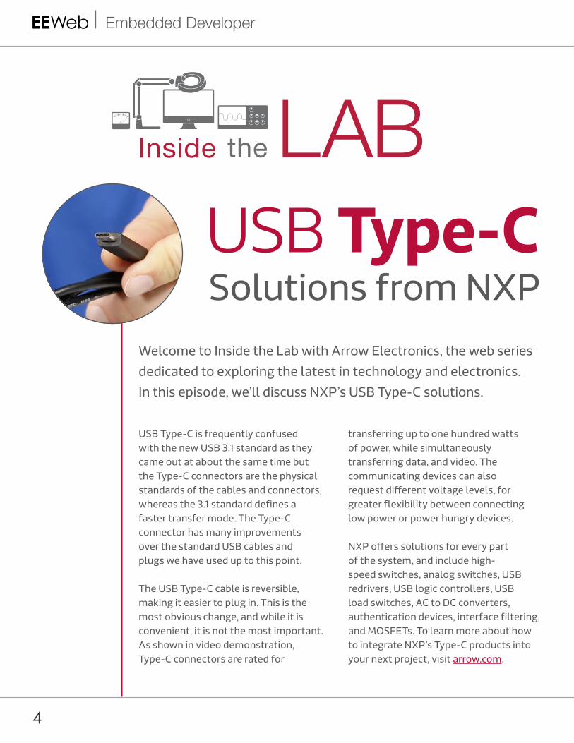
USB Type-C Solutions from NXP
Welcome to Inside the Lab with Arrow Electronics, the web series dedicated to exploring the latest in technology and electronics. In this episode, we’ll discuss NXP’s USB Type-C solutions.
USB Type-C is frequently confused with the new USB 3.1 standard as they came out at about the same time but the Type-C connectors are the physical standards of the cables and connectors, whereas the 3.1 standard defines a faster transfer mode. The Type-C connector has many improvements over the standard USB cables and plugs we have used up to this point.
The USB Type-C cable is reversible, making it easier to plug in. This is the most obvious change, and while it is convenient, it is not the most important. As shown in video demonstration, Type-C connectors are rated for
transferring up to one hundred watts of power, while simultaneously transferring data, and video. The communicating devices can also request different voltage levels, for greater flexibility between connecting low power or power hungry devices.
NXP offers solutions for every part of the system, and include high-speed switches, analog switches, USB redrivers, USB logic controllers, USB load switches, AC to DC converters, authentication devices, interface filtering, and MOSFETs. To learn more about how to integrate NXP’s Type-C products into your next project, visit arrow.com.
PRODUCT WATCH
5
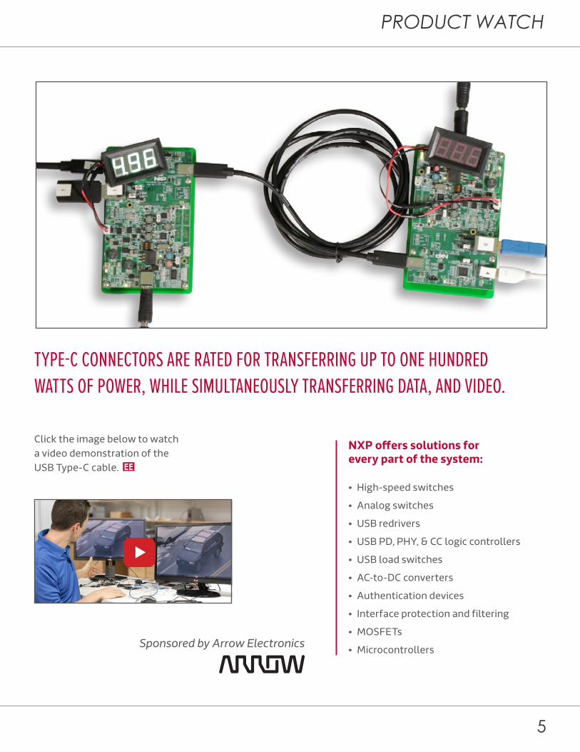
TYPE-C CONNECTORS ARE RATED FOR TRANSFERRING UP TO ONE HUNDRED WATTS OF POWER, WHILE SIMULTANEOUSLY TRANSFERRING DATA, AND VIDEO.
Sponsored by Arrow Electronics
Click the image below to watch a video demonstration of the USB Type-C cable.
NXP offers solutions for every part of the system:
• High-speed switches
• Analog switches
• USB redrivers
• USB PD, PHY, & CC logic controllers
• USB load switches
• AC-to-DC converters
• Authentication devices
• Interface protection and filtering
• MOSFETs
• Microcontrollers
6
Embedded Developer
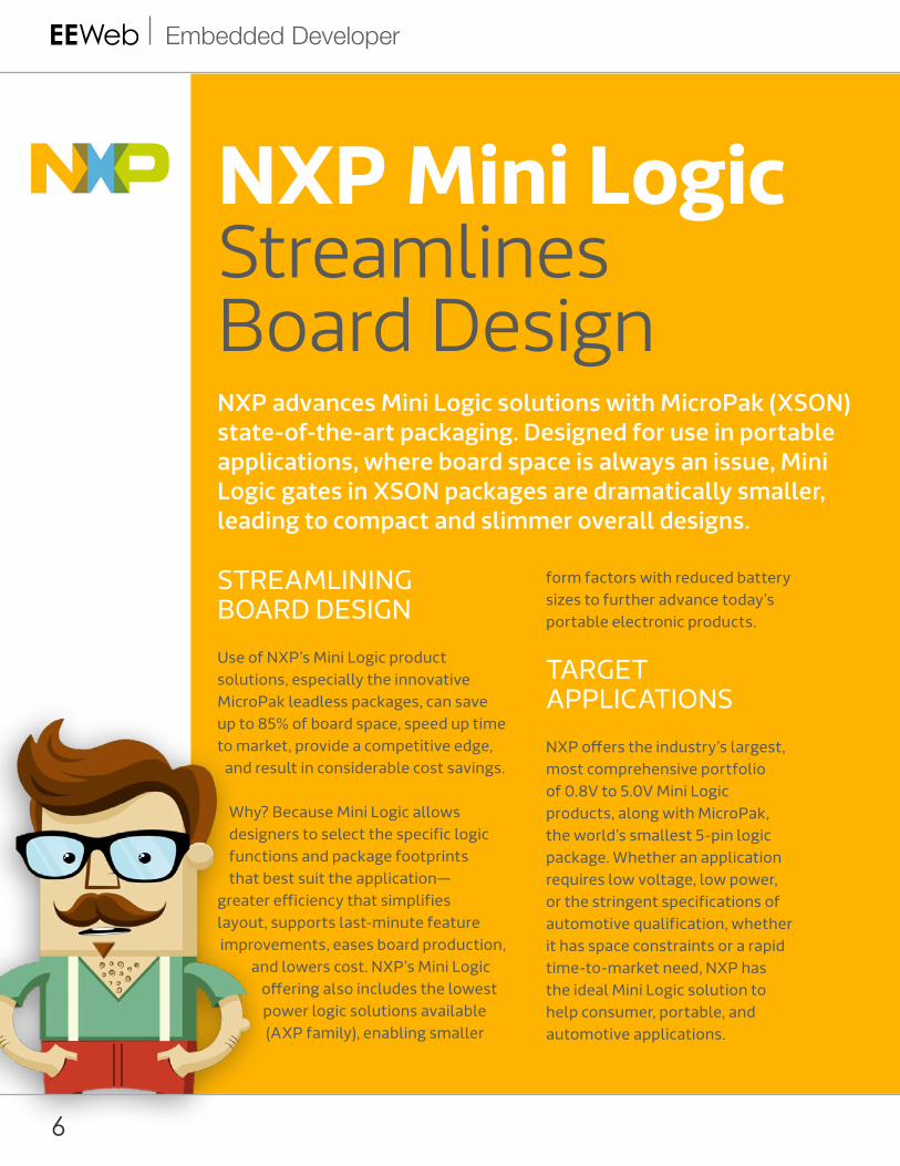
STREAMLINING BOARD DESIGN
Use of NXP’s Mini Logic product solutions, especially the innovative MicroPak leadless packages, can save up to 85% of board space, speed up time to market, provide a competitive edge,
and result in considerable cost savings.
Why? Because Mini Logic allows designers to select the specific logic functions and package footprints that best suit the application—
greater efficiency that simplifies layout, supports last-minute feature improvements, eases board production,
and lowers cost. NXP’s Mini Logic offering also includes the lowest power logic solutions available (AXP family), enabling smaller
NXP Mini Logic Streamlines Board Design
form factors with reduced battery sizes to further advance today’s portable electronic products.
TARGET APPLICATIONS
NXP offers the industry’s largest, most comprehensive portfolio of 0.8V to 5.0V Mini Logic products, along with MicroPak, the world’s smallest 5-pin logic package. Whether an application requires low voltage, low power, or the stringent specifications of automotive qualification, whether it has space constraints or a rapid time-to-market need, NXP has the ideal Mini Logic solution to help consumer, portable, and automotive applications.
NXP advances Mini Logic solutions with MicroPak (XSON) state-of-the-art packaging. Designed for use in portable applications, where board space is always an issue, Mini Logic gates in XSON packages are dramatically smaller, leading to compact and slimmer overall designs.
PRODUCT WATCH
7
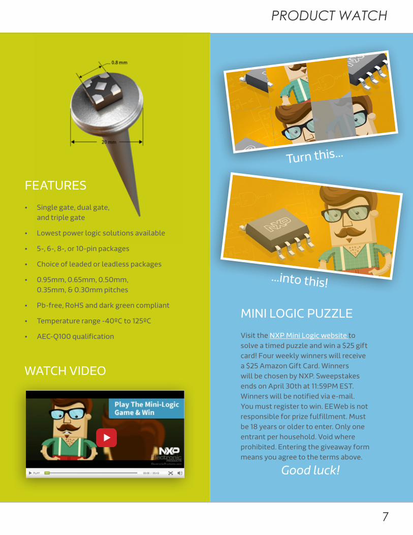
FEATURES
• Single gate, dual gate, and triple gate
• Lowest power logic solutions available
• 5-, 6-, 8-, or 10-pin packages
• Choice of leaded or leadless packages
• 0.95mm, 0.65mm, 0.50mm, 0.35mm, & 0.30mm pitches
• Pb-free, RoHS and dark green compliant
• Temperature range -40ºC to 125ºC
• AEC-Q100 qualification
MINI LOGIC PUZZLE
Visit the NXP Mini Logic website to solve a timed puzzle and win a $25 gift card! Four weekly winners will receive a $25 Amazon Gift Card. Winners will be chosen by NXP. Sweepstakes ends on April 30th at 11:59PM EST. Winners will be notified via e-mail. You must register to win. EEWeb is not responsible for prize fulfillment. Must be 18 years or older to enter. Only one entrant per household. Void where prohibited. Entering the giveaway form means you agree to the terms above.
Good luck!
WATCH VIDEO
Turn this...
...into this!

8
Embedded Developer
AXP Translators
In order to reduce power dissipation in electronic applications there is a trend toward lower supply voltages. A consequence of this trend is a necessity to interface in modular designs between applications at different supply voltages.
In order to reduce power dissipation in electronic applications there is a trend toward lower supply voltages. A consequence of this trend is a necessity to interface in modular designs between applications at different supply voltages.
NXP has added innovative voltage level translating devices to its existing Advanced eXtremely low Power (AXP) logic family to further improve its portfolio of translator products. These translating gates ensure interface compatibility of new lower voltage designs to existing products without serious power dissipation penalties.
The AXP family of Si-gate CMOS devices uses leading low threshold process technology and next generation packaging technology to create extremely small functions that support the trend to very low operating voltage and consume very little power. The AXP translators are level translating gates targeted at small footprint portable applications. They are available in single (1G), dual (2G), and triple (3G) gate Mini Logic formats. Multiple standard and configurable logic functions are included in the AXP translators. These are made available in the industries smallest packages.
WATCH VIDEO TRANSLATOR QUIZ
CLICH HERE to take the NXP Translator Quiz
PRODUCT WATCH
9
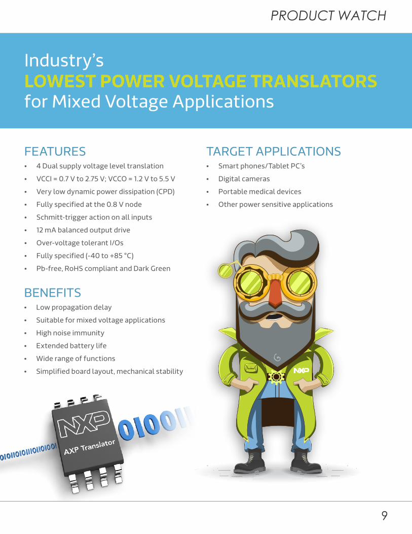
Industry’s LOWEST POWER VOLTAGE TRANSLATORS for Mixed Voltage Applications
FEATURES• 4 Dual supply voltage level translation
• VCCI = 0.7 V to 2.75 V; VCCO = 1.2 V to 5.5 V
• Very low dynamic power dissipation (CPD)
• Fully specified at the 0.8 V node
• Schmitt-trigger action on all inputs
• 12 mA balanced output drive
• Over-voltage tolerant I/Os
• Fully specified (-40 to +85 °C)
• Pb-free, RoHS compliant and Dark Green
BENEFITS• Low propagation delay
• Suitable for mixed voltage applications
• High noise immunity
• Extended battery life
• Wide range of functions
• Simplified board layout, mechanical stability
TARGET APPLICATIONS• Smart phones/Tablet PC’s
• Digital cameras
• Portable medical devices
• Other power sensitive applications

10
Embedded Developer
The High Cost of COMPLIANCE
TECH REPORT
11
How Embedded Module Standards can inhibit true Design Freedom
By Wolfgang Heinz-Fischer Head of Marketing and PR, TQ-Group
There are two predominant architectures in the module market: Intel (x86 and Atom) and ARM, and each have “Standards” defined by different user groups. Standards have their place, particularly in the Intel world where one licensee has ensured compatibility over many years. However, developers in the ARM world are discovering that often
limitations imposed by standards far outweigh their benefits. This article will explore the role of
standards and weigh the pros and cons of implementing them in both the
Intel and ARM worlds.
12
Embedded Developer
The Intel market is characterized by standards, primarily COM Express and Qseven. (There are other standards, but as they are older and less in use today, they are not referred to in this article). Standards are a funny thing and in some case ‘in the eye of the beholder’. There are at least 3 COM Express standards: Type 2, Type-6 and Type-10.
All standards are meant to deliver:
• Compatibility in dimension, functions, signals, timings and software
• Interchangeability between different suppliers and different chip vendors
For the user this means that they develop an application board, which follows the standard, so they can choose from different manufacturers and simply attach the module. If they need more power, they simply take the correspondingly more powerful module
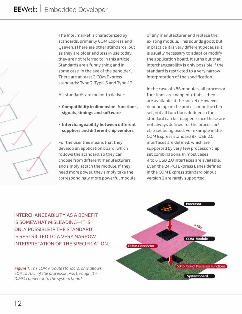
of any manufacturer and replace the existing module. This sounds good; but in practice it is very different because it is usually necessary to adapt or modify the application board. It turns out that interchangeability is only possible if the standard is restricted to a very narrow interpretation of the specification.
In the case of x86 modules, all processor functions are mapped, (that is, they are available at the socket). However depending on the processor or the chip set, not all functions defined in the standard can be mapped, since these are not always defined for the processor/chip set being used. For example in the COM Express standard 8x, USB 2.0 interfaces are defined, which are supported by very few processor/chip set combinations. In most cases, 4 to 6 USB 2.0 interfaces are available. Even the 24 PCI Express Lanes defined in the COM Express standard pinout version 2 are rarely supported.
INTERCHANGEABILITY AS A BENEFIT IS SOMEWHAT MISLEADING—IT IS ONLY POSSIBLE IF THE STANDARD IS RESTRICTED TO A VERY NARROW INTERPRETATION OF THE SPECIFICATION.
Figure 1. The COM Module standard, only allows 50% to 70% of the processor pins through the DIMM connector to the system board.
TECH REPORT
13
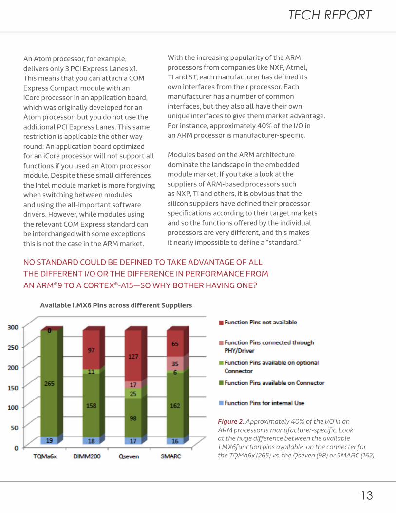
With the increasing popularity of the ARM processors from companies like NXP, Atmel, TI and ST, each manufacturer has defined its own interfaces from their processor. Each manufacturer has a number of common interfaces, but they also all have their own unique interfaces to give them market advantage. For instance, approximately 40% of the I/O in an ARM processor is manufacturer-specific.
Modules based on the ARM architecture dominate the landscape in the embedded module market. If you take a look at the suppliers of ARM-based processors such as NXP, TI and others, it is obvious that the silicon suppliers have defined their processor specifications according to their target markets and so the functions offered by the individual processors are very different, and this makes it nearly impossible to define a “standard.”
NO STANDARD COULD BE DEFINED TO TAKE ADVANTAGE OF ALL THE DIFFERENT I/O OR THE DIFFERENCE IN PERFORMANCE FROM AN ARM®9 TO A CORTEX®-A15—SO WHY BOTHER HAVING ONE?
Figure 2. Approximately 40% of the I/O in an ARM processor is manufacturer-specific. Look at the huge difference between the available 1.MX6function pins available on the connecter for the TQMa6x (265) vs. the Qseven (98) or SMARC (162).
An Atom processor, for example, delivers only 3 PCI Express Lanes x1. This means that you can attach a COM Express Compact module with an iCore processor in an application board, which was originally developed for an Atom processor; but you do not use the additional PCI Express Lanes. This same restriction is applicable the other way round: An application board optimized for an iCore processor will not support all functions if you used an Atom processor module. Despite these small differences the Intel module market is more forgiving when switching between modules and using the all-important software drivers. However, while modules using the relevant COM Express standard can be interchanged with some exceptions this is not the case in the ARM market.
Available i.MX6 Pins across different Suppliers
14
Embedded Developer
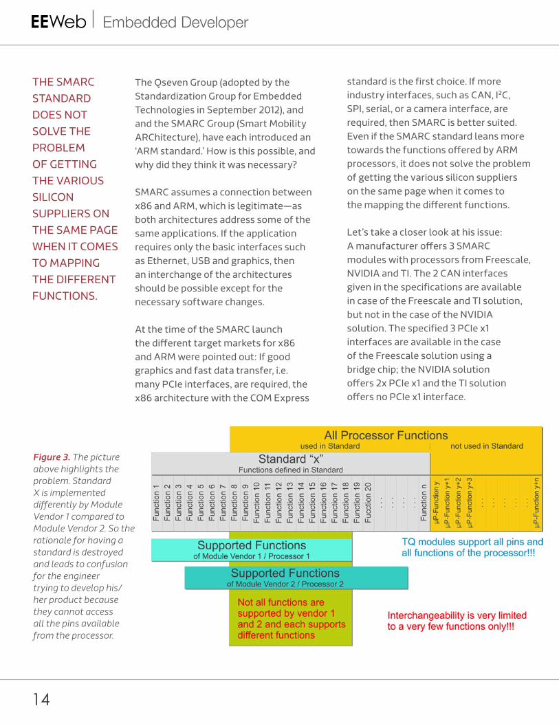
Figure 3. The picture above highlights the problem. Standard X is implemented differently by Module Vendor 1 compared to Module Vendor 2. So the rationale for having a standard is destroyed and leads to confusion for the engineer trying to develop his/her product because they cannot access all the pins available from the processor.
The Qseven Group (adopted by the Standardization Group for Embedded Technologies in September 2012), and and the SMARC Group (Smart Mobility ARChitecture), have each introduced an ‘ARM standard.’ How is this possible, and why did they think it was necessary?
SMARC assumes a connection between x86 and ARM, which is legitimate—as both architectures address some of the same applications. If the application requires only the basic interfaces such as Ethernet, USB and graphics, then an interchange of the architectures should be possible except for the necessary software changes.
At the time of the SMARC launch the different target markets for x86 and ARM were pointed out: If good graphics and fast data transfer, i.e. many PCIe interfaces, are required, the x86 architecture with the COM Express
standard is the first choice. If more industry interfaces, such as CAN, I²C, SPI, serial, or a camera interface, are required, then SMARC is better suited. Even if the SMARC standard leans more towards the functions offered by ARM processors, it does not solve the problem of getting the various silicon suppliers on the same page when it comes to the mapping the different functions.
Let’s take a closer look at his issue: A manufacturer offers 3 SMARC modules with processors from Freescale, NVIDIA and TI. The 2 CAN interfaces given in the specifications are available in case of the Freescale and TI solution, but not in the case of the NVIDIA solution. The specified 3 PCIe x1 interfaces are available in the case of the Freescale solution using a bridge chip; the NVIDIA solution offers 2x PCIe x1 and the TI solution offers no PCIe x1 interface.
THE SMARC STANDARD DOES NOT SOLVE THE PROBLEM OF GETTING THE VARIOUS SILICON SUPPLIERS ON THE SAME PAGE WHEN IT COMES TO MAPPING THE DIFFERENT FUNCTIONS.
TECH REPORT
15
This raises the question about the real interchangeability of modules from a manufacturer, which all follow the SMARC standard. And how do the new interfaces such as USB 3.0 reappear in the latest standards? Are there then new standards or new definitions and are these compatible with the previous standards? In case of ARM modules, a switch from one architecture or one supplier to another has an additional hurdle – the software drivers. What is still quite easy in case of x86 systems, does not work in the ARM world. Every module supplier, even if it is the same processor based on the same standard as another supplier, has their own BSP. Thus, this part must be modified or developed anew.
Standards in the ARM module market are always compromised in regards to the available interfaces at the module socket. Depending on the standard and the processor being used, access to a number of processor functions is limited—even though you are paying for them. And should the processor offer the required functions in a future variant, the question remains whether these functions are then supported by the module.
DEPENDING ON THE STANDARD AND THE PROCESSOR BEING USED, ACCESS TO MANY PROCESSOR FUNCTIONS IS LIMITED—EVEN THOUGH YOU ARE PAYING FOR THEM.
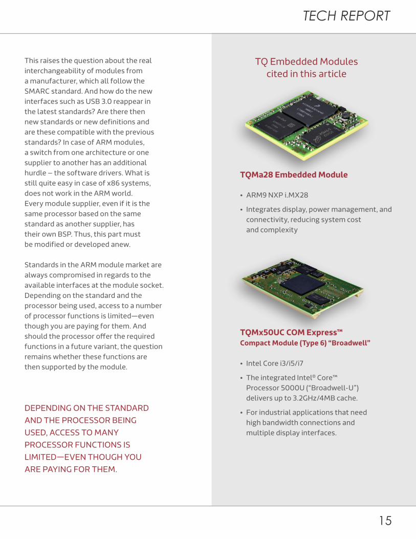
TQMa28 Embedded Module
• ARM9 NXP i.MX28
• Integrates display, power management, and connectivity, reducing system cost and complexity
TQMx50UC COM Express™ Compact Module (Type 6) “Broadwell”
• Intel Core i3/i5/i7
• The integrated Intel® Core™ Processor 5000U (“Broadwell-U”) delivers up to 3.2GHz/4MB cache.
• For industrial applications that need high bandwidth connections and multiple display interfaces.
TQ Embedded Modules cited in this article
16
Embedded Developer
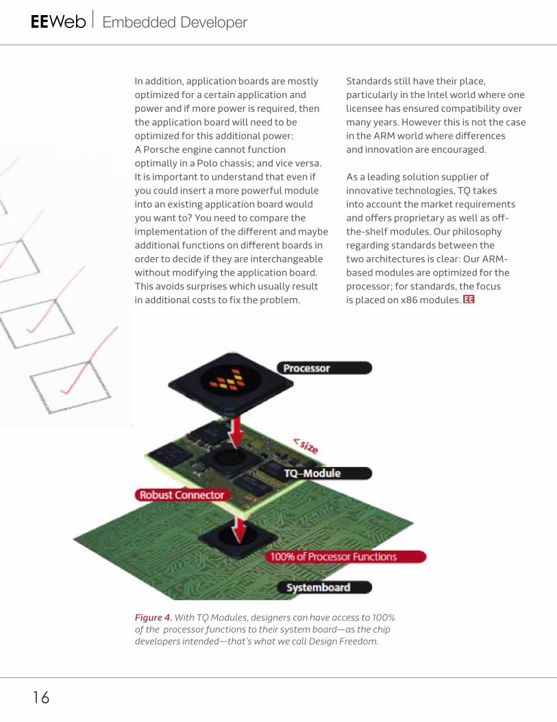
In addition, application boards are mostly optimized for a certain application and power and if more power is required, then the application board will need to be optimized for this additional power: A Porsche engine cannot function optimally in a Polo chassis; and vice versa. It is important to understand that even if you could insert a more powerful module into an existing application board would you want to? You need to compare the implementation of the different and maybe additional functions on different boards in order to decide if they are interchangeable without modifying the application board. This avoids surprises which usually result in additional costs to fix the problem.
Figure 4. With TQ Modules, designers can have access to 100% of the processor functions to their system board—as the chip developers intended—that’s what we call Design Freedom.
Standards still have their place, particularly in the Intel world where one licensee has ensured compatibility over many years. However this is not the case in the ARM world where differences and innovation are encouraged.
As a leading solution supplier of innovative technologies, TQ takes into account the market requirements and offers proprietary as well as off-the-shelf modules. Our philosophy regarding standards between the two architectures is clear: Our ARM-based modules are optimized for the processor; for standards, the focus is placed on x86 modules.

Schematics.com
Your Circuit Starts Here.Sign up to design, share, and collaborate
on your next project—big or small.
Click Here to Sign Up
18
Embedded Developer
DEVELOPMENT Picks up the Pace with PIC® Microcontrollers
TECH REPORT
19
When considering a microcontroller for your
system’s hardware design, many factors
must be considered. Although specifications
and performance metrics are important, they only
tell part of the story. Any hardware design engineer
can attest that ease of development, scalability, and
excellent engineering support are invaluable to the
successful release of any microcontroller (MCU)-based
product. Microchip addresses these concerns through
shared peripheral support across the PIC MCU product
family, so code becomes more reusable. Development is
also simplified via a unified and completely free MPLAB®
Integrated Development Environment (IDE) which
supports all PIC MCUs. And of course any PIC MCU
also comes along with a host of technical
documentation, software examples,
hardware reference designs,
and highly responsive
customer support.
20
Embedded Developer
Microchip is a leader in the microcontroller market, offering a complete range of microcontroller devices. The 8-bit MCU families include the PIC10, PIC12, PIC16, and PIC18 series of MCUs. The 16-bit families include PIC24 MCUs and dsPIC33 Digital Signal Controllers (DSCs). The 32-bit PIC32 family offers the highest performance and the largest integrated memories in the PIC product line 8-bit MCUs have a pin count ranging from 6 to 100 pins, 16-bit MCUs have a pin count ranging from 14 to 144 pins, and 32-bit MCUs have a pin count ranging from 28 to 144 pins. Performance scales from a maximum of 16 MIPS in 8-bit MCUs, through a maximum of 70 MIPS in 16-bit MCUs, up to a maximum of 330 DMIPS for 32-bit MCUs. Integrated Flash (non-volatile) memory capacity varies similarly, with a range of 0.5-128KB for 8-bit, a range of 4-1024KB for 16-bit, and a range of 16KB to 2MB for 32-bit MCUs.
Microchip PIC MCUs offer the widest operating ranges available. The supply voltage input can range from 1.8V to 5.5V. Some device families support an ambient temperature of up to 150°C. Additionally, the eXtreme Low Power (XLP) 8-bit and 16-bit PIC MCUs offer industry-leading power consumption performance over a full range of package sizes. Run currents start at only 30 µA/MHz (8-bit) and 150 µA/MHz (16-bit), while sleep currents are as low as 9 nA. If outright performance is the goal, the Microchip 16-bit and
32-bit PIC MCU families offer the industry’s highest performance. If small form factors are paramount, packaged parts as small as the 8-pin 2 × 3 DFN are available. Microchip also continues to improve its product offerings: since 2009, over 140 new PIC MCUs have been added to the product portfolio, offering a range of industry-critical technologies such as integrated security engines, advanced analog capabilities and Core Independent Peripherals (CIP). Low-cost options abound, with MCUs supporting USB and 192-pixel segmented display drivers available for less than $1 (in quantity).
One key benefit of the Microchip PIC MCU ecosystem is the strong scalability between microcontroller families. Some integrated peripherals are available across the entire portfolio, such as Capture/Compare/PWM, timers, comparators, I2C, SPI, UART and touch sensing. Beginning with the 8-bit PIC16 MCU family, peripheral support is available for Intelligent Analog (Op Amp, DAC, and 12-bit ADC), USB, motor control, and segmented LCD. PIC18 devices and above support the CAN bus, and PIC24 devices and above also support integrated graphics drivers. Ethernet support is available on the PIC18 and PIC32 MCU families. These integrated peripherals do more than reduce CPU overhead, lower bill-of-materials (BOM) cost, and enable smaller system PCB sizes.
One key benefit of the Microchip PIC
MCU ecosystem is the strong
scalability between
microcontroller families.
TECH REPORT
21
Because the peripheral support is shared amongst many of the PIC MCU families, there is reduced development overhead. In addition, many PIC MCU families share pinout/package footprints.
Therefore, the development code doesn’t need to change when interchanging PIC MCU designs. As a result, the system architect can spend less time worrying about the selection of the specific PIC MCU at the onset of the design. When more specifics are known about the product later in the design cycle, the microcontroller can easily be scaled without losing development effort. MCUs with the same pinout/footprint can even be scaled without impacting PCB layout.
As alluded to earlier, hardware specifications alone don’t win over the hardware/system design engineer. So perhaps the most compelling argument in favor of Microchip PIC MCUs over alternative solutions is their shared development environment. In fact, every MCU within Microchip’s expansive product portfolio (900+ components) is supported by the free MPLAB IDE. The
latest version, known as MPLAB X IDE, is now based on the open-source NetBeans platform. It includes cross-platform support for Mac OS X®, Linux® and Microsoft Windows® operating system software. MPLAB X IDE also includes new features such as “one click” for automatically making, programming and running/debugging code on the PIC MCU, support for multiple compiler versions/debug tool versions, and improvements to the user interface of the MPLAB GUI.
MPLAB X IDE can be used for project management, code development, MCU programming and also code debugging. It not only provides a single IDE for development and debug of all
22
Embedded Developer
Microchip PIC MCUs, but also provides a wide range of standard code libraries, including TCP/IP stacks and USB drivers. Many compilers are supported, including MPLAB XC8 (C compiler for 8-bit PIC devices), MPLAB XC16 (C compiler for 16-bit PIC devices), and MPLAB XC32 (C/C++ compiler for 32-bit devices). The MPLAB IDE also is supported by many third-party devices (PICAXE, etc.). In essence, this means code is easily portable between MCUs, reducing the amount of new code that must be developed and enabling the reuse of existing code.
Excellent support is a necessity for timely product deployment. Microchip has hundreds of highly trained application engineers on staff, who can assist in debugging technical issues as well as provide insight into the more advanced features within the ecosystem of MCUs and software tools. Microchip and their global distribution network offers support to customers of all sizes. In addition, PIC MCU customers have access to numerous reference designs and low-cost development boards for rapid product prototyping. Many example software programs are available for becoming familiar with MPLAB X IDE. Microchip also offers extensive technical documentation and application notes for thorough assistance with implementing PIC MCU features and capabilities. Even more assistance is available through Microchip’s comprehensive training resources,
which include web seminars, hands-on training sessions, “lunch & learns”, and customer conferences. Microchip’s online forums provide a convenient and simple way for individuals to interact with the large, global community of over 60,000+ engineers and developers using PIC MCUs in their own systems.
As of 2015, the total embedded systems market continues to grow. Pre-existing markets such as energy meters and monitoring, lighting, security, automotive, and smartphone accessories are still expanding. New markets such as medical instruments and Internet of Things (IoT) devices promise even more applications for embedded systems. Meeting the demand for such a wide variety of embedded system designs will require companies to leverage internal software and hardware development across multiple different product lines. Engineering and development resources must be used efficiently for reduced product time-to-market. Selecting Microchip PIC MCUs for your system design provides you with industry-leading hardware performance, scalability due to pin and code compatibility, and easier, platform-independent code development via the free MPLAB IDE which supports all Microchip MCUs. As a result, you will benefit from easier design-in and a more effective use of development resources, which will significantly speed your product’s time to market easier design-in.
The Microchip name and logo, the Microchip logo, dsPIC, MPLAB, and PIC are registered trademarks of Microchip Technology Incorporated in the U.S.A. and other countries. All other trademarks mentioned herein are property of their respective companies.
© 2016, Microchip Technology Incorporated, All Rights Reserved.
Microchip has hundreds of highly trained application engineers on staff,
who can assist in debugging
technical issues as well as provide
insight into the more advanced features within the ecosystem of MCUs and
software tools.
24
Embedded Developer
{Part 6}
PIDCONTROLLERS
MIXING SIGNALS:An Introduction to
By Sree Harsha Angara Cypress Semiconductor
To read the previous article in this series, click the image above.
In the last few columns, I went through some of the math to explain
exactly what compensation entails, as well as how PID compensation works.
In this column, I will cover working with analog compensators and brush
lightly on digital compensation (which will be covered in more detail in the
next installment).
Typically, when building a closed-loop system, an engineer is faced with
the choice of picking an analog or digital compensator. In the past, analog
compensation was the de facto selection for making fast closed loops. However,
in recent years, the use of digital compensators has grown rapidly due to the
availability of fast microcontrollers with integrated ADCs. In addition, many
applications require compensation for a wide variety of peripheral functions like
monitoring, communication protocols, and so forth. Integrating all of these into
a single microcontroller saves board space and cost when compared to using
dedicated analog ICs as controllers.
{Part 5}
PIDCONTROLLERS
MIXING SIGNALS:An Introduction to The Agony
of Choice
By Sree Harsha Angara Cypress Semiconductor
To read the previous article in this series, click the image above.
In the previous article, I showed how to compensate simple
first-order systems. As a quick recap, a Proportional-Integral
(PI) controller is all that is needed for compensating
first-order systems perfectly. By perfectly, I mean that
you can theoretically achieve any combination of crossover
frequencies and phase margins. There is, of course, an
entertaining mathematical proof for this, but it is not
needed for the purposes of implementation.
We will now move to second-order systems, which constitute
the vast majority of practical systems. At last, we come to
unveiling the full Proportional-Integral-Derivative (PID)
compensator and its implications.
{Part 4}
PIDCONTROLLERS
MIXING SIGNALS:An Introduction to The PID
Compensator
By Sree Harsha Angara Cypress Semiconductor
To read the previous article in this series, click the image above.
In my previous column, I showed bode plots for different types of transfer functions. I also touched on the basic principles of closed loop systems. As a refresher, the gain crossover frequency dictates the speed of the controller, and ensuring a phase margin of around 70 degrees achieves a nice trade-off between the overshoot and speed. Now I’d like to look at how different compensators affect the characteristics of the plant. In the course of this discussion though, we will see that not all systems need a full-blown proportional-integral-derivative compensator (PID compensator). Most of the time, a PI compensator or even a simple integral controller can do the job. Knowing which type of compensator to use cannot only reduce the complexity of an implementation, it also helps give a clear understanding of the exact requirements of the complete system. In other words, we don’t want to add stuff in if it doesn’t help. In this part of the series, I’ll cover compensating first-order systems. Just remember that, as mentioned earlier, sometimes higher-order systems, which have dominant first-order characteristics, can fit the bill. For example, most thermal systems typically exhibit a very dominant first-order behavior.
{Part 3}
PIDCONTROLLERS
MIXING SIGNALS:An Introduction to
The P, the I, and the PIBy Sree Harsha Angara Cypress Semiconductor
To read the previous article in this series, click the image above.
BPIDCONTROLLERSMIXING SIGNALS:An Introduction to TRANSFER FUNCTIONS Squiggly Lines Mean?
First-Order Systems
Compensating
Second-order SystemsCompensating
Analog or Digital Compensation
TECH SERIES
25
In the last installment, we were halfway through the compensator
design for a buck converter. As a quick recap, when designing
digital compensators, the true system gain is different from the
derived transfer function. In the case of our buck converter, we
have to take into consideration the voltage sense resistive divider
drop, the ADC digitization gain, and the PWM gain. Ignoring these
will likely end up with an extremely slow compensator or worse,
a compensator that is unstable.
Digital PID Compensation
Implementation and Quirks

26
Embedded Developer
Synchronous Buck Compensator Design
We left the compensator design at the transfer function,
Now the system gain is,
In the example, the ADC resolution is set to 8-bits with a voltage reference of 2.048V. Note that normally we go 12-bits or higher, but in this case I’ve limited it to 8-bits as the buck runs at 200KHz, which locks the PWM period to 240 (running off a 48MHz clock). Having more resolution than the minimum step size of the PWM gives rise to limit cycling, more of which I’ll be covering later in the article.
The resistive divider is set to 220k and 49k which scales the voltage down to,
So the equivalent transfer function will come to,
For the above transfer function we can design the compensator for with the steps mentioned in Part 4.
Figure 1. Synchronous Buck System gains block diagram
TECH SERIES
27
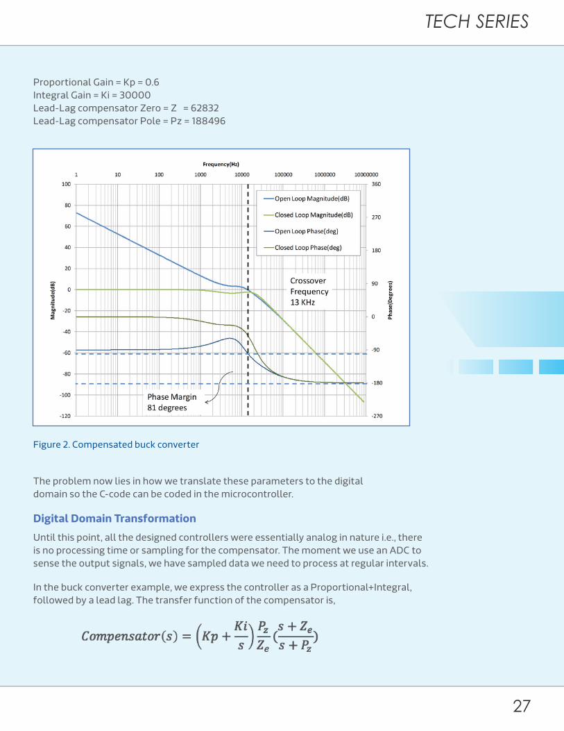
Proportional Gain = Kp = 0.6 Integral Gain = Ki = 30000 Lead-Lag compensator Zero = Z = 62832 Lead-Lag compensator Pole = Pz = 188496
Figure 2. Compensated buck converter
The problem now lies in how we translate these parameters to the digital domain so the C-code can be coded in the microcontroller.
Digital Domain Transformation
Until this point, all the designed controllers were essentially analog in nature i.e., there is no processing time or sampling for the compensator. The moment we use an ADC to sense the output signals, we have sampled data we need to process at regular intervals.
In the buck converter example, we express the controller as a Proportional+Integral, followed by a lead lag. The transfer function of the compensator is,
28
Embedded Developer
The simplest way to change the function into digital domain (also called z-domain) is to replace
Where Ts is the sampling time (or ADC sampling frequency).
The above is called the rectangular approximation. There are those who swear by the more commonly used bi-linear transform, but for our case this approximation works just fine (primarily as the sampling time doesn’t go high enough to cause ringing artifacts). Either transformation will give similar results; the choice is yours.
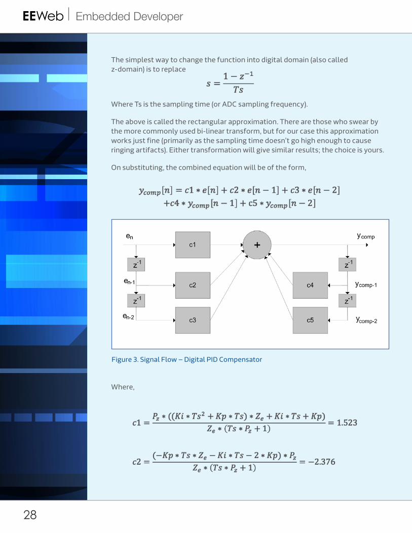
On substituting, the combined equation will be of the form,
Where,
Figure 3. Signal Flow – Digital PID Compensator
TECH SERIES
29
The term indicates the current value of the compensator output i.e., what we should write to the PWM duty cycle register. and indicate the historical values of the compensator output. Similarly, indicates the current error value while and are the historical values of error.
Note that the coefficients are floating points. To realize these in a fixed function processor, we use the traditional approach of left shifting all the coefficients by a few bits (20 in this case), and finally right shifting them back before writing to the PWM duty cycle register. Remember to take care that the registers don’t overflow during the multiplications.
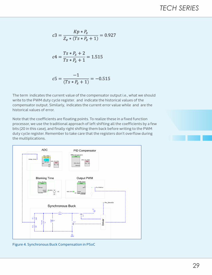
Figure 4. Synchronous Buck Compensation in PSoC
30
Embedded Developer
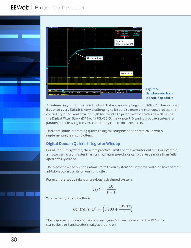
An interesting point to note is the fact that we are sampling at 200KHz. At these speeds (i.e., once every 5uS), it is very challenging to be able to enter an interrupt, process the control equation, and have enough bandwidth to perform other tasks as well. Using the Digital Filter Block (DFB) of a PSoC 3/5, the whole PID control loop executes in a parallel path, leaving the CPU completely free to do other tasks.
There are some interesting quirks to digital compensation that turn up when implementing real controllers.
Digital Domain Quirks: Integrator Windup
For all real-life systems, there are practical limits on the actuator output. For example, a motor cannot run faster than its maximum speed, nor can a valve be more than fully open or fully closed.
The moment we apply saturation limits to our system actuator, we will also have some additional constraints on our controller.
For example, let us take our previously designed system:
Whose designed controller is,
The response of this system is shown in Figure 6. It can be seen that the PID output starts close to 6 and settles finally at around 0.1.
Figure 5. Synchronous buck closed loop control
TECH SERIES
31
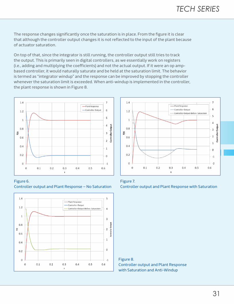
The response changes significantly once the saturation is in place. From the figure it is clear that although the controller output changes it is not reflected to the input of the plant because of actuator saturation.
On top of that, since the integrator is still running, the controller output still tries to track the output. This is primarily seen in digital controllers, as we essentially work on registers (i.e., adding and multiplying the coefficients) and not the actual output. If it were an op amp-based controller, it would naturally saturate and be held at the saturation limit. The behavior is termed as “integrator windup” and the response can be improved by stopping the controller whenever the saturation limit is exceeded. When anti-windup is implemented in the controller, the plant response is shown in Figure 8.
Figure 6. Controller output and Plant Response – No Saturation
Figure 7. Controller output and Plant Response with Saturation
Figure 8. Controller output and Plant Response with Saturation and Anti-Windup
32
Embedded Developer
Digital Domain Quirks – Limit Cycling
Digitization essentially quantizes the states in which the controller can exist; i.e., the output can be a 1 or a 2, not values in between. In other words, the minimum step size the control signal can change is fixed. If the smallest variation on the input of the system results in a variation greater than the minimum variation in output sensing, the system has the potential to oscillate about a 1-lsb error. This is referred to as limit cycling.
To illustrate limit cycling, say we have a 12-bit ADC with a range of 0 to 1.024V, and it measures the output voltage of a 5V, 8-bit PWM feeding a R-C circuit. Assuming the R-C values are large enough to filter out the PWM frequency, the output voltage is simply equal to,
Fixing our reference at 360mV, the duty cycle needed to achieve this will be,
The ADC reading is given by,
For a 360mV reference, the reading will be,
TECH SERIES
33
Since the compare value for the PWM can only increase with a minimum step size of 1, the closest value of duty cycle it can achieve will be 7% (at 18 counts) and 7.4% (at 19 counts).
So, the controller will keep overshooting/undershooting the settling point owing to the digital nature of the controller. This leads to an oscillator behavior around the settling point that we termed earlier as limit cycling. Whenever designing digital controllers, care must be taken to ensure that the minimum change in the control signal will result in a variation lesser than the minimum change in the output sensor.
Final Thoughts
The concept of PID control has been around for a long time without a great deal of change to the core concepts. Sure, we adapted them to the digital domain, but the design aspects are largely unchanged. The amount of existing literature and readily available IP and embedded code is one of the primary reasons why the PID controller is still widely used. Add to that the flexibility of mixed signal controllers like PSoC 5LP and you end up with a very powerful tool for building fast acting closed loop systems as well as communication and housekeeping functions integrated in a single chip.
PWM Compare
Value
Output Voltage
ADC Reading
Error (Counts)
17 351.6mV 1406 +34
18 371.1mV 1484 -44
embeddeddev
Your Guide to Embedded MCUs and Development Tools.
w w w . e m b e d d e d d e v e l o p e r . c o m
Everything you’re looking for in one place.
36
Embedded Developer
TQ AM335 Embedded modules provide attitude control for a low-cost Star Tracker for sounding rockets, balloons and Class D Satellites
By J. W. Percival, K. Nordsieck, K. P. Jaehnig, Space Astronomy Laboratory, University of Wisconsin, Madison
Edited by Glenn ImObersteg, Convergence Promotions
and the Star Tracker ST5000
Embedded Modules

COVER STORY
37
By J. W. Percival, K. Nordsieck, K. P. Jaehnig, Space Astronomy Laboratory, University of Wisconsin, Madison
Edited by Glenn ImObersteg, Convergence Promotions
The University of Wisconsin-Madison Dept. of
Astronomy’s Space Astronomy Laboratory has
built and flown an imaging device that provides
autonomous (”Lost in Space”) inertial attitude
determination, 10Hz star tracking, and digital imaging
with embedded compression (Percival & Nordsieck,
ADASS X, v. 238, p. 463, Percival et al., Proc. SPIE
Vol. 4013, p. 394-400.) The attitude determination
subsystem uses a 30-square-degree field of view
and an embedded star catalog to determine the right
ascension and declination of its line of sight to about
1-arcsecond. The star tracking subsystem generates
inertial attitude quaternions at 10Hz. The digital
imaging subsystem uses a scheme of “progressive
image transmission” in which the image is sent
out over a very-low-bandwidth channel, such as a
spacecraft telemetry downlink, in such a way that it
can be reconstructed “on the fly” and updated as more
data arrive. Large (> 1Mb) images can be obtained over
a 4-kbit downlink in as little as 10 seconds.
38
Embedded Developer
In-Flight Performance
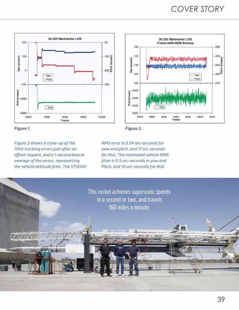
Figures 1 and 2 compare normal sequential transmission with Progressive Image Transmission. Figure 1 shows a line-by-line transmission over a 2400 baud link after 60 seconds. Note the tiny bit of received image at the bottom. The right image shows the same amount of data, over the same 2400 baud link, also after 60 seconds. Progressive Image Transmission has delivered information at all spatial and intensity scales, allowing a rapid assessment of the image content. The ST5000 has flown on 9 sounding rocket flights, during the last 3 of which it was actively controlling the rocket. The flight
This photo shows a sounding rocket on the launcher (the horizontal truss) before it is raised to the vertical launch position. Starting from the right, there is the 1st stage Terrier, the black 2nd stage Brant, the Styrofoam box keeping the sun off the science payload (a telescope), and Attitude Control System (ACS) section by the gas canisters, where the TQ AM335 Module is located. Ahead of that is a short brown-colored section, which provides stability guidance through the turbulent lower layers of the atmosphere, and ahead of that is the parachute section and nose cone.
data shown in Figures 1 and 2 is from the 12-Aug-2007 sounding rocket flight (36.220) of a far-ultraviolet spectrograph investigating the scattering and extinction properties of dust and gas. The first figure shows the tracking errors over the whole 360-second science portion of the flight. The X-axis is plotted in 10-Hz frames. The widely spaced vertical dots at frame 6500 represent the slew from the blind, gyro-based initial pointing to the experimenter’s target, a slew controlled by the ST5000’s inertial attitude determination. The step-like changes reflect real-time offset requests uplinked by the experimenter to move the target around in the experiment’s focal plane.
This rocket achieves supersonic speeds in a second or two, and travels 160 miles a minute. We observe through the trajectory arc at the top for around 500 seconds, then re-enter, plunge in free-fall to 35,000 feet, and open the chute. The CPU module runs from 12 minutes before launch, all the way through impact on the desert floor. Then it loses power, and the mission is over. The team then recovers the systems, inspect, and re-fly.
Anatomy of a Rocket
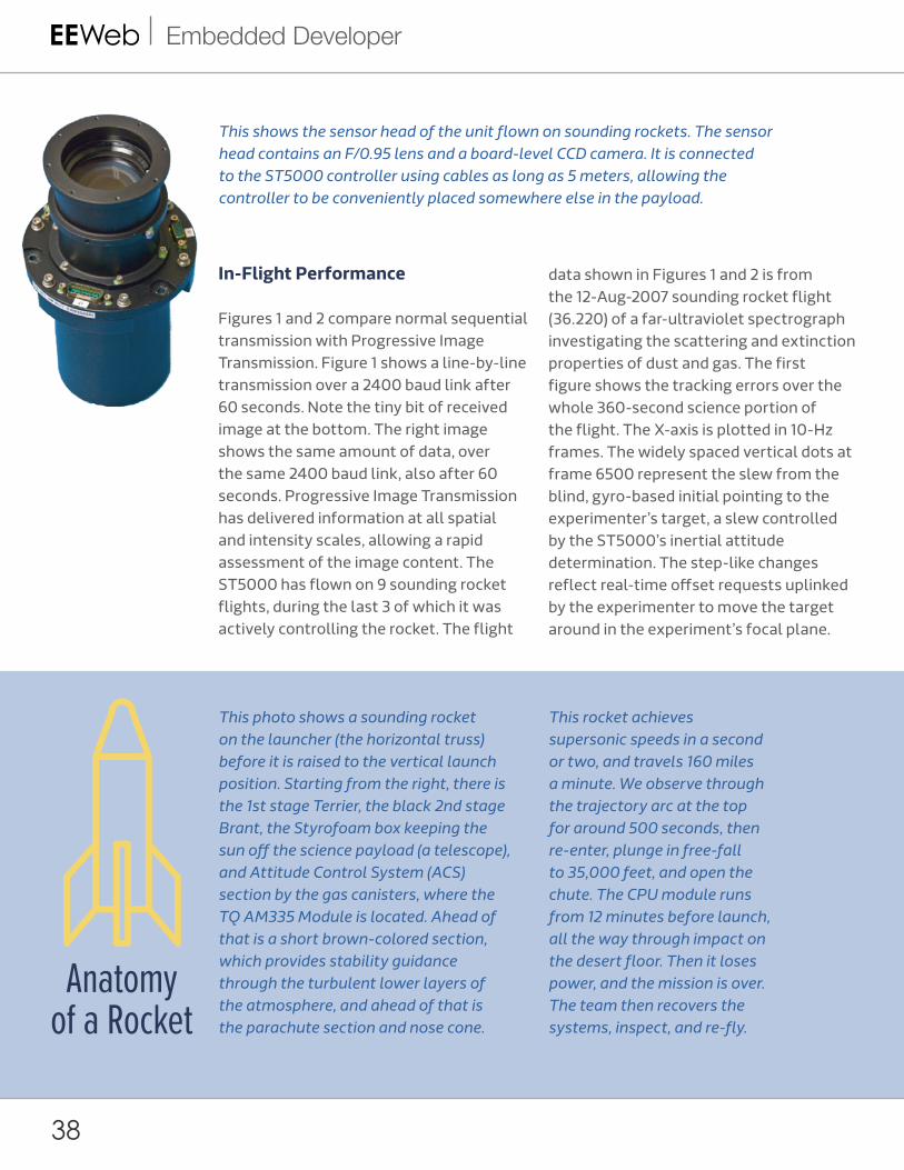
This shows the sensor head of the unit flown on sounding rockets. The sensor head contains an F/0.95 lens and a board-level CCD camera. It is connected to the ST5000 controller using cables as long as 5 meters, allowing the controller to be conveniently placed somewhere else in the payload.
COVER STORY
39
Figure 1. Figure 2.
Figure 2 shows a close-up of the 10Hz tracking errors just after an offset request, and a 1-second boxcar average of the errors, representing the vehicle attitude jitter. The ST5000
RMS error is 0.54 arc-seconds for yaw and pitch, and 17 arc-seconds for Roll. The estimated vehicle RMS jitter is 0.5 arc-seconds in yaw and Pitch, and 10 arc-seconds for Roll.
This rocket achieves supersonic speeds in a second or two, and travels
160 miles a minute.
40
Embedded Developer
Attitude Determination
The ST5000 can determine its attitude with respect to an absolute coordinate system (say, FK5 Equatorial) by analyzing the star patterns in a single frame. It can do so without any a-priori knowledge of attitude or image orientation. The determination is insensitive to stray objects in the field such as glints, hot pixels, airplanes, satellites, or asteroids. It does not depend on star brightness, colors, or any knowledge of the sensor’s spectral sensitivity.
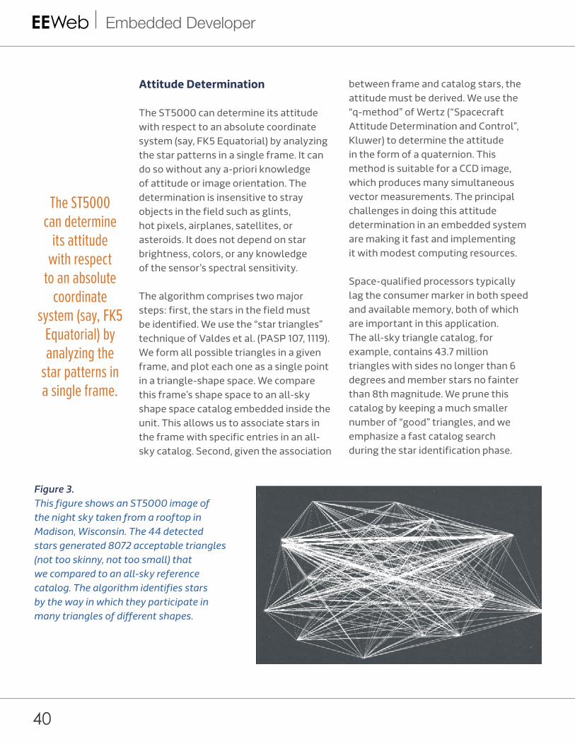
The algorithm comprises two major steps: first, the stars in the field must be identified. We use the “star triangles” technique of Valdes et al. (PASP 107, 1119). We form all possible triangles in a given frame, and plot each one as a single point in a triangle-shape space. We compare this frame’s shape space to an all-sky shape space catalog embedded inside the unit. This allows us to associate stars in the frame with specific entries in an all-sky catalog. Second, given the association
between frame and catalog stars, the attitude must be derived. We use the “q-method” of Wertz (“Spacecraft Attitude Determination and Control”, Kluwer) to determine the attitude in the form of a quaternion. This method is suitable for a CCD image, which produces many simultaneous vector measurements. The principal challenges in doing this attitude determination in an embedded system are making it fast and implementing it with modest computing resources.
Space-qualified processors typically lag the consumer marker in both speed and available memory, both of which are important in this application. The all-sky triangle catalog, for example, contains 43.7 million triangles with sides no longer than 6 degrees and member stars no fainter than 8th magnitude. We prune this catalog by keeping a much smaller number of “good” triangles, and we emphasize a fast catalog search during the star identification phase.
Figure 3. This figure shows an ST5000 image of the night sky taken from a rooftop in Madison, Wisconsin. The 44 detected stars generated 8072 acceptable triangles (not too skinny, not too small) that we compared to an all-sky reference catalog. The algorithm identifies stars by the way in which they participate in many triangles of different shapes.
The ST5000 can determine
its attitude with respect
to an absolute coordinate
system (say, FK5 Equatorial) by analyzing the
star patterns in a single frame.
COVER STORY
41
Progressive Image Transmission
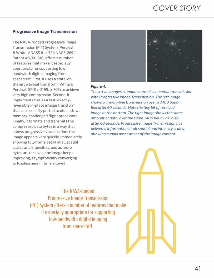
The NASA-funded Progressive Image Transmission (PIT) System (Percival & White, ADASS II, p. 321; NAG5-2694; Patent #5,991,816) offers a number of features that make it especially appropriate for supporting low-bandwidth digital imaging from spacecraft. First, it uses a state-of-the-art wavelet transform (White & Percival, SPIE v. 2199, p. 703) to achieve very high compression. Second, it implements this as a fast, exactly-reversible in-place integer transform that can be easily ported to older, slower memory-challenged flight processors. Finally, it formats and transmits the compressed data bytes in a way that allows progressive visualization: the image appears very quickly, immediately showing full-frame detail at all spatial scales and intensities, and as more bytes are received, the image keeps improving, asymptotically converging to losslessness (if time allows).
Figure 4. These two images compare normal sequential transmission with Progressive Image Transmission. The left image shows a line-by-line transmission over a 2400 baud link after 60 seconds. Note the tiny bit of received image at the bottom. The right image shows the same amount of data, over the same 2400 baud link, also after 60 seconds. Progressive Image Transmission has delivered information at all spatial and intensity scales, allowing a rapid assessment of the image content.
The NASA-funded Progressive Image Transmission
(PIT) System offers a number of features that make it especially appropriate for supporting
low-bandwidth digital imaging from spacecraft.
42
Embedded Developer
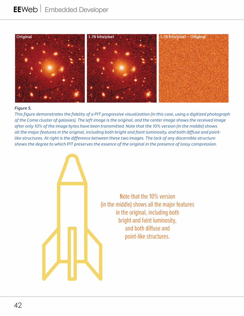
Figure 5. This figure demonstrates the fidelity of a PIT progressive visualization (in this case, using a digitized photograph of the Coma cluster of galaxies). The left image is the original, and the center image shows the received image after only 10% of the image bytes have been transmitted. Note that the 10% version (in the middle) shows all the major features in the original, including both bright and faint luminosity, and both diffuse and point-like structures. At right is the difference between these two images. The lack of any discernible structure shows the degree to which PIT preserves the essence of the original in the presence of lossy compression.
Note that the 10% version (in the middle) shows all the major features
in the original, including both bright and faint luminosity,
and both diffuse and point-like structures.

COVER STORY
43
Super Comet as tracked by the Star Tracker
Acknowledgements and Contacts
The ST5000 was designed with the support of NASA grants NAG5-7026 and NAG5-8588. The authors thank NASA’a Sounding Rocket Project Office for continuing operational support and flight opportunities. For more information on the TQ AM335, contact Vaughn Orchard: [email protected], or go to www.embeddedmodules.net.
Videos
“Star Tracker” Tracks Comet ISON
Super Comet ISON 2013 - Sounding Rockets
The Texas Instruments’ TQ AM335 Embedded Module used in the payload of the ST5000 has a ARM® Cortex®-A8 TI AM335 “Sitara” Processor and is ideal for Home and building automation, portable navigation and consumer electronics.
44
Embedded Developer
Microchip’s MPLAB Xpress Cloud-Based IDE Provides a Free Development Platform
45
EEWeb FEATURE
Microchip’s newly launched MPLAB Xpress
is a cloud-based integrated development
environment (IDE) aimed at giving developers
easy access to the tools environment on
any Internet-connected computer or tablet.
MPLAB Xpress contains the most popular
features of the MPLAB X IDE, allowing
programmers to easily move between the two
environments. MPLAB Xpress is the first of its
kind to offer a GUI-based code generator:
the MPLAB Code Configurator 3.0.
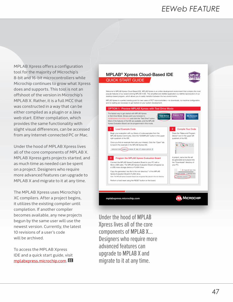
QUICK START GUIDEMPLAB® Xpress Cloud-Based IDE
Welcome to MPLAB Xpress Cloud-Based IDE. MPLAB Xpress is an online development environment that contains the most popular features of our award-winning MPLAB X IDE. This simplified and distilled application is a faithful reproduction of our desktop-based program, which allows you to easily transition between the two environments.MPLAB Xpress is a perfect starting point for new users of PIC® microcontrollers—no downloads, no machine configuration, and no waiting are necessary to get started on your system development.
OPTION 1: Preview MPLAB Xpress with Test Drive Mode
Load Example CodeBegin your evaluation with our library of code examples from the MPLAB Xpress Community. Click the “EXAMPLES” button in the upper right quadrant of the IDE.
Once you find an example that suits your interest, Click the “Open” tab to launch the example in the MPLAB Xpress IDE.
Program the MPLAB Xpress Evaluation BoardConnect the MPLAB Xpress Evaluation Board to your PC with a Micro-USB cable. The MPLAB Xpress Evaluation Board will appear as a USB mass storage device or FLASH drive.
Copy the generated .hex file to the root directory** of the MPLAB Xpress Evaluation Board’s FLASH drive. Note: The MPLAB Xpress Evaluation Board only recognizes files placed in the root directory.
Perform a hard reset using the RESET button on the board.
The fastest way to get started with MPLAB Xpress is Test Drive Mode. Simply point your browser to mplabxpress.microchip.com and click the “Test Drive” button. Most of the features of the IDE are available, and the MPLAB Xpress Evaluation Board can be programmed in this mode.
1 Compile Your CodePress the “Make and Program Device” icon in the upper left quadrant of the IDE.
A project_name.hex file will be generated and placed into the "Downloads" directory of your PC.
2
3
mplabxpress.microchip.com
46
Embedded Developer
It’s easy for users to get started on MPLAB Xpress because they do not have to download or configure their
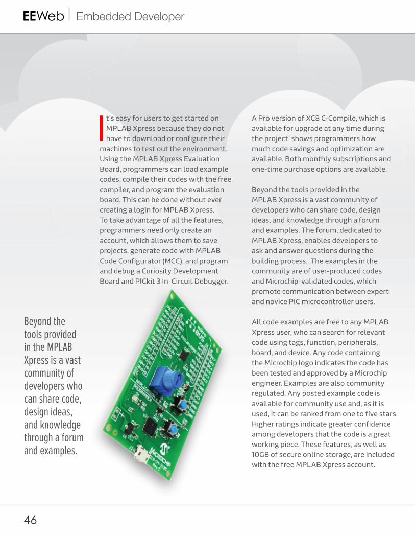
machines to test out the environment. Using the MPLAB Xpress Evaluation Board, programmers can load example codes, compile their codes with the free compiler, and program the evaluation board. This can be done without ever creating a login for MPLAB Xpress. To take advantage of all the features, programmers need only create an account, which allows them to save projects, generate code with MPLAB Code Configurator (MCC), and program and debug a Curiosity Development Board and PICkit 3 In-Circuit Debugger.
A Pro version of XC8 C-Compile, which is available for upgrade at any time during the project, shows programmers how much code savings and optimization are available. Both monthly subscriptions and one-time purchase options are available.
Beyond the tools provided in the MPLAB Xpress is a vast community of developers who can share code, design ideas, and knowledge through a forum and examples. The forum, dedicated to MPLAB Xpress, enables developers to ask and answer questions during the building process. The examples in the community are of user-produced codes and Microchip-validated codes, which promote communication between expert and novice PIC microcontroller users.
All code examples are free to any MPLAB Xpress user, who can search for relevant code using tags, function, peripherals, board, and device. Any code containing the Microchip logo indicates the code has been tested and approved by a Microchip engineer. Examples are also community regulated. Any posted example code is available for community use and, as it is used, it can be ranked from one to five stars. Higher ratings indicate greater confidence among developers that the code is a great working piece. These features, as well as 10GB of secure online storage, are included with the free MPLAB Xpress account.
Beyond the tools provided in the MPLAB Xpress is a vast community of developers who can share code, design ideas, and knowledge through a forum and examples.
47
EEWeb FEATURE
MPLAB Xpress offers a configuration tool for the majority of Microchip’s 8-bit and 16-bit microcontrollers while Microchip continues to grow what Xpress does and supports. This tool is not an offshoot of the version in Microchip’s MPLAB X. Rather, it is a full MCC that was constructed in a way that can be either compiled as a plugin or a Java web start. Either compilation, which provides the same functionality with slight visual differences, can be accessed from any Internet-connected PC or Mac.
Under the hood of MPLAB Xpress lives all of the core components of MPLAB X. MPLAB Xpress gets projects started, and as much time as needed can be spent on a project. Designers who require more advanced features can upgrade to MPLAB X and migrate to it at any time.
The MPLAB Xpress uses Microchip’s XC compilers. After a project begins, it utilizes the existing compiler until completion. If another compiler becomes available, any new projects begun by the same user will use the newest version. Currently, the latest 10 revisions of a user’s code will be archived.
To access the MPLAB Xpress IDE and a quick start guide, visit mplabxpress.microchip.com.
QUICK START GUIDEMPLAB® Xpress Cloud-Based IDE
Welcome to MPLAB Xpress Cloud-Based IDE. MPLAB Xpress is an online development environment that contains the most popular features of our award-winning MPLAB X IDE. This simplified and distilled application is a faithful reproduction of our desktop-based program, which allows you to easily transition between the two environments.
MPLAB Xpress is a perfect starting point for new users of PIC® microcontrollers—no downloads, no machine configuration, and no waiting are necessary to get started on your system development.
OPTION 1: Preview MPLAB Xpress with Test Drive Mode
Load Example Code
Begin your evaluation with our library of code examples from the MPLAB Xpress Community. Click the “EXAMPLES” button in the upper right quadrant of the IDE.
Once you find an example that suits your interest, Click the “Open” tab to launch the example in the MPLAB Xpress IDE.
Program the MPLAB Xpress Evaluation Board
Connect the MPLAB Xpress Evaluation Board to your PC with a Micro-USB cable. The MPLAB Xpress Evaluation Board will appear as a USB mass storage device or FLASH drive.
Copy the generated .hex file to the root directory** of the MPLAB Xpress Evaluation Board’s FLASH drive. Note: The MPLAB Xpress Evaluation Board only recognizes files placed in the root directory.
Perform a hard reset using the RESET button on the board.
The fastest way to get started with MPLAB Xpress is Test Drive Mode. Simply point your browser to mplabxpress.microchip.com and click the “Test Drive” button. Most of the features of the IDE are available, and the MPLAB Xpress Evaluation Board can be programmed in this mode.
1 Compile Your Code
Press the “Make and Program Device” icon in the upper left quadrant of the IDE.
A project_name.hex file will be generated and placed into the "Downloads" directory of your PC.
2
3
mplabxpress.microchip.com
Under the hood of MPLAB Xpress lives all of the core components of MPLAB X...Designers who require more advanced features can upgrade to MPLAB X and migrate to it at any time.

Click here
Sierra Circuits:A Complete PCB Resource
PLUS: The Ground ” Myth in PrintedCircuits
“
PCB Resin Reactor+
Ken BahlCEO of Sierra Circuits
Let There Be
How Cree reinvented the light bulb
LIGHT
David ElienVP of Marketing & Business
Development, Cree, Inc.
New LED Filament Tower
Cutting Edge Flatscreen Technologies
+
+
M o v i n g T o w a r d s
a Clean Energy
FUTURE— Hugo van Nispen, COO of DNV KEMA
MCU Wars 32-bit MCU Comparison
Cutting Edge
SPICEModeling
Freescale and TI Embedded
Modules
ARMCortex
Programming
From Concept to
Reality Wolfgang Heinz-Fischer
Head of Marketing & PR, TQ-Group
Low-Power Design Techniques
TQ-Group’s Comprehensive Design Process
+
+
PowerDeveloper
Octobe r 20 13
Designing forDurability
View more EEWeb magazines— Click Here