Embed Size (px)
DESCRIPTION
MicroBlaze Aplication
Citation preview
FPGA and ASIC Technology Comparison - 1
© 2009 Xilinx, Inc. All Rights Reserved
Embedded Design with the MicroBlaze Soft Processor Core
© 2007 Xilinx, Inc. All Rights ReservedFPGA and ASIC Technology Comparison - 2
© 2007 Xilinx, Inc. All Rights ReservedFPGA and ASIC Technology Comparison - 2
© 2009 Xilinx, Inc. All Rights Reserved
Welcome
If you are new to Embedded design with Xilinx FPGA’s, this module will explain why you may want to use the MicroBlaze soft processor core in any of our FPGA families
Understanding the basics of MicroBlaze is important if you are going to take full advantage of its features
The Embedded Developers Kit software (EDK) is designed to make building a fast embedded design easy
© 2007 Xilinx, Inc. All Rights ReservedFPGA and ASIC Technology Comparison - 3
© 2007 Xilinx, Inc. All Rights ReservedFPGA and ASIC Technology Comparison - 3
© 2009 Xilinx, Inc. All Rights Reserved
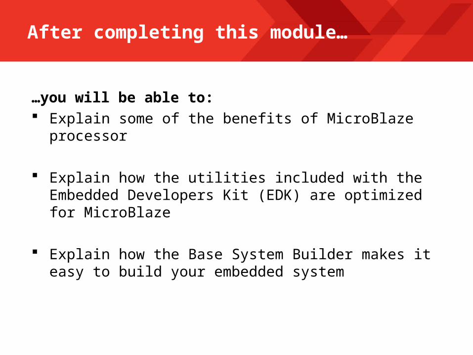
After completing this module…
…you will be able to: Explain some of the benefits of MicroBlaze processor
Explain how the utilities included with the Embedded Developers Kit (EDK) are optimized for MicroBlaze
Explain how the Base System Builder makes it easy to build your embedded system
© 2007 Xilinx, Inc. All Rights ReservedFPGA and ASIC Technology Comparison - 4
© 2007 Xilinx, Inc. All Rights ReservedFPGA and ASIC Technology Comparison - 4
© 2009 Xilinx, Inc. All Rights Reserved
Hardware Overview MicroBlaze Base System Builder Summary
Lessons
© 2007 Xilinx, Inc. All Rights ReservedFPGA and ASIC Technology Comparison - 5
© 2007 Xilinx, Inc. All Rights ReservedFPGA and ASIC Technology Comparison - 5
© 2009 Xilinx, Inc. All Rights Reserved
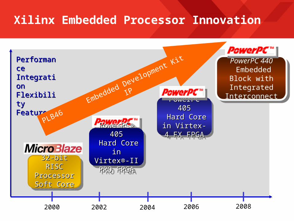
Xilinx Embedded Processor Innovation
PerformancePerformanceIntegration Integration FlexibilityFlexibilityFeatures Features
32-bit RISC32-bit RISCProcessorProcessorSoft CoreSoft Core
32-bit RISC32-bit RISCProcessorProcessorSoft CoreSoft Core
PLB46 Embedded Development Kit
IP PowerPC 440 Embedded Block with
Integrated Interconnect
PowerPC 440 Embedded Block with
Integrated Interconnect
PowerPC® 405PowerPC® 405 Hard CoreHard Corein Virtex®-II in Virtex®-II PRO FPGAPRO FPGA
PowerPC® 405PowerPC® 405 Hard CoreHard Corein Virtex®-II in Virtex®-II PRO FPGAPRO FPGA
2000 2002 2004 20082006
PowerPC 405PowerPC 405 Hard CoreHard Core
in Virtex-4 FX in Virtex-4 FX FPGAFPGA
PowerPC 405PowerPC 405 Hard CoreHard Core
in Virtex-4 FX in Virtex-4 FX FPGAFPGA
© 2007 Xilinx, Inc. All Rights ReservedFPGA and ASIC Technology Comparison - 6
© 2007 Xilinx, Inc. All Rights ReservedFPGA and ASIC Technology Comparison - 6
© 2009 Xilinx, Inc. All Rights Reserved
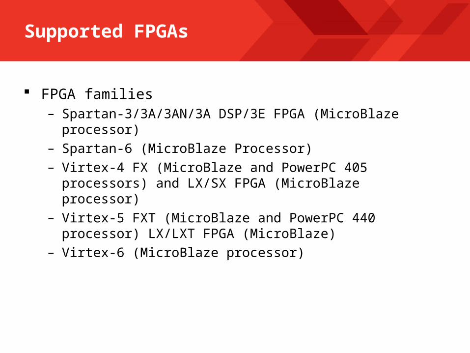
Supported FPGAs
FPGA families– Spartan-3/3A/3AN/3A DSP/3E FPGA (MicroBlaze processor)– Spartan-6 (MicroBlaze Processor)– Virtex-4 FX (MicroBlaze and PowerPC 405 processors) and LX/SX FPGA
(MicroBlaze processor)– Virtex-5 FXT (MicroBlaze and PowerPC 440 processor) LX/LXT FPGA
(MicroBlaze)– Virtex-6 (MicroBlaze processor)

© 2007 Xilinx, Inc. All Rights ReservedFPGA and ASIC Technology Comparison - 7
© 2007 Xilinx, Inc. All Rights ReservedFPGA and ASIC Technology Comparison - 7
© 2009 Xilinx, Inc. All Rights Reserved
Embedded Design in an FPGA
Embedded design in an FPGA can consist of the following– FPGA hardware design
• Processor system– MicroBlaze processor (soft core)– PowerPC processor (PPC440 hard core)– PLB or PLB v46 bus– PLB bus components
• Other FPGA hardware– Peripherals can either be custom made by the user with a Xilinx bus interface
or a library of pre-optimized peripherals are available
© 2007 Xilinx, Inc. All Rights ReservedFPGA and ASIC Technology Comparison - 8
© 2007 Xilinx, Inc. All Rights ReservedFPGA and ASIC Technology Comparison - 8
© 2009 Xilinx, Inc. All Rights Reserved
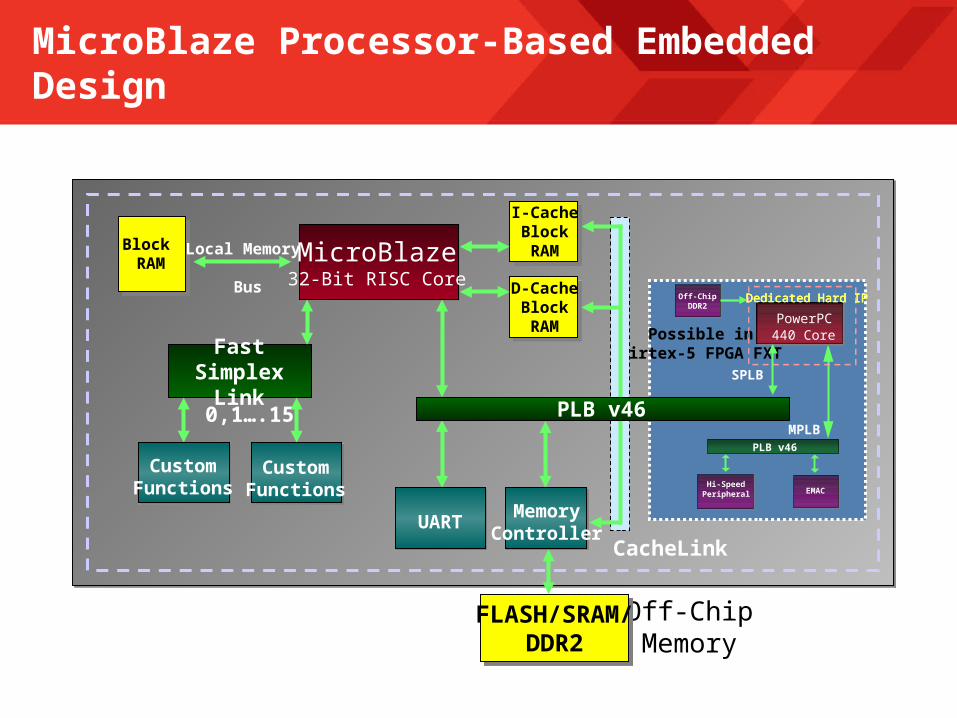
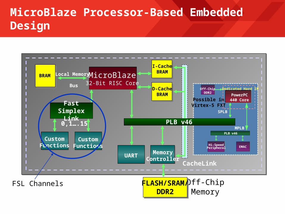
MicroBlaze Processor-Based Embedded Design
MicroBlaze32-Bit RISC Core
UARTMemory
Controller
Off-ChipMemory
FLASH/SRAM/DDR2
Fast Simplex Link
0,1….15
CustomFunctions
CustomFunctions
Block RAM
Local Memory
Bus D-CacheBlockRAM
I-CacheBlockRAM
Possible inVirtex-5 FPGA FXT
CacheLink
PLB v46
MPLB
PowerPC405 Core
Dedicated Hard IP
PowerPC405 Core
Dedicated Hard IP
PowerPC405 Core
Dedicated Hard IP
PowerPC440 Core
Dedicated Hard IP
EMACHi-Speed
Peripheral
SPLB
PLB v46
Off-ChipDDR2
© 2007 Xilinx, Inc. All Rights ReservedFPGA and ASIC Technology Comparison - 9
© 2007 Xilinx, Inc. All Rights ReservedFPGA and ASIC Technology Comparison - 9
© 2009 Xilinx, Inc. All Rights Reserved
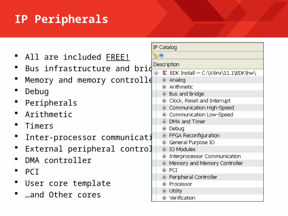
IP Peripherals
All are included FREE! Bus infrastructure and bridge cores Memory and memory controller cores Debug Peripherals Arithmetic Timers Inter-processor communication External peripheral controller DMA controller PCI User core template …and Other cores
© 2007 Xilinx, Inc. All Rights ReservedFPGA and ASIC Technology Comparison - 10
© 2007 Xilinx, Inc. All Rights ReservedFPGA and ASIC Technology Comparison - 10
© 2009 Xilinx, Inc. All Rights Reserved
Hardware Overview MicroBlaze Base System Builder Summary
Lessons
© 2007 Xilinx, Inc. All Rights ReservedFPGA and ASIC Technology Comparison - 11
© 2007 Xilinx, Inc. All Rights ReservedFPGA and ASIC Technology Comparison - 11
© 2009 Xilinx, Inc. All Rights Reserved
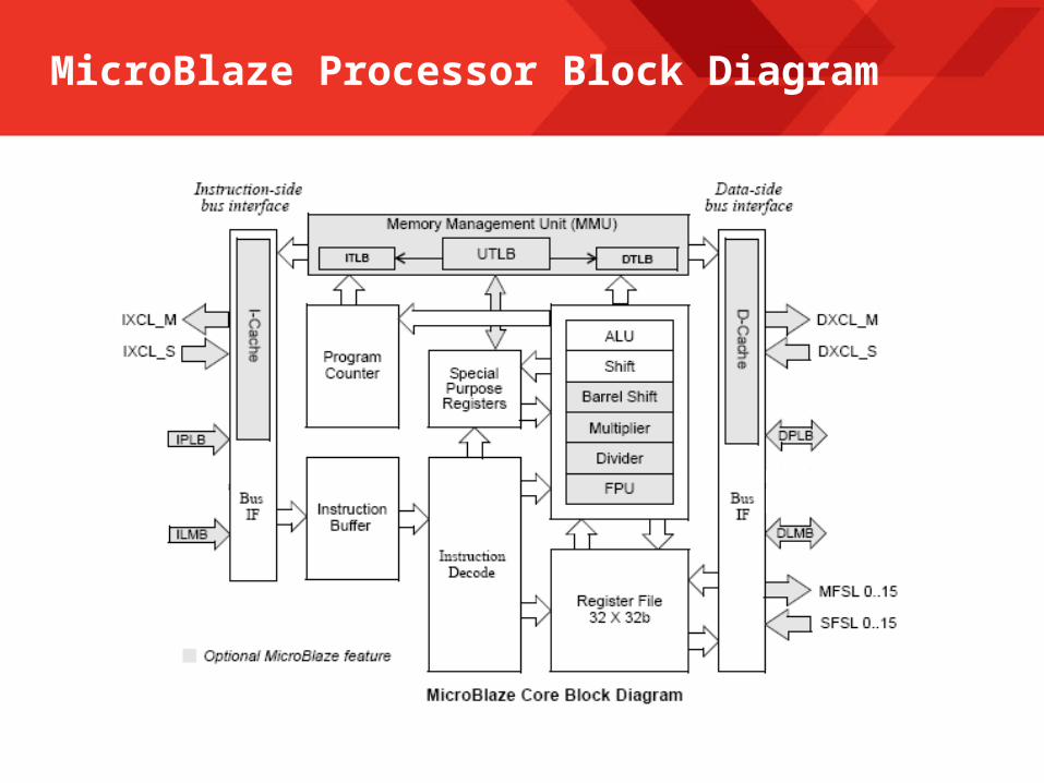
MicroBlaze Processor Block Diagram
© 2007 Xilinx, Inc. All Rights ReservedFPGA and ASIC Technology Comparison - 12
© 2007 Xilinx, Inc. All Rights ReservedFPGA and ASIC Technology Comparison - 12
© 2009 Xilinx, Inc. All Rights Reserved
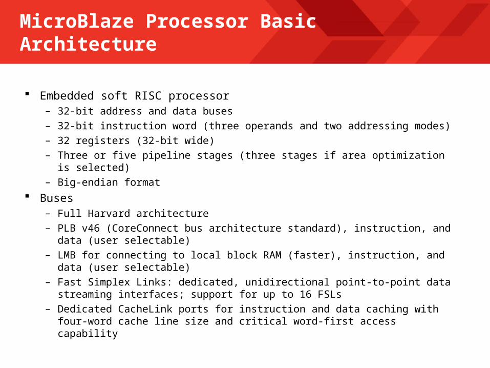
MicroBlaze Processor Basic Architecture
Embedded soft RISC processor– 32-bit address and data buses– 32-bit instruction word (three operands and two addressing modes)– 32 registers (32-bit wide)– Three or five pipeline stages (three stages if area optimization is selected)– Big-endian format
Buses– Full Harvard architecture– PLB v46 (CoreConnect bus architecture standard), instruction, and data (user selectable)– LMB for connecting to local block RAM (faster), instruction, and data (user selectable)– Fast Simplex Links: dedicated, unidirectional point-to-point data streaming interfaces;
support for up to 16 FSLs– Dedicated CacheLink ports for instruction and data caching with four-word cache line
size and critical word-first access capability
© 2007 Xilinx, Inc. All Rights ReservedFPGA and ASIC Technology Comparison - 13
© 2007 Xilinx, Inc. All Rights ReservedFPGA and ASIC Technology Comparison - 13
© 2009 Xilinx, Inc. All Rights Reserved
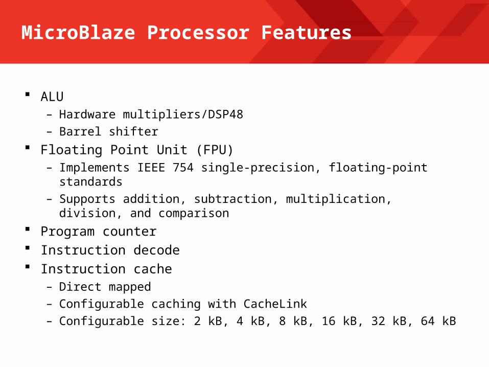
MicroBlaze Processor Features
ALU– Hardware multipliers/DSP48– Barrel shifter
Floating Point Unit (FPU)– Implements IEEE 754 single-precision, floating-point standards– Supports addition, subtraction, multiplication, division, and comparison
Program counter Instruction decode Instruction cache
– Direct mapped– Configurable caching with CacheLink– Configurable size: 2 kB, 4 kB, 8 kB, 16 kB, 32 kB, 64 kB

© 2007 Xilinx, Inc. All Rights ReservedFPGA and ASIC Technology Comparison - 14
© 2007 Xilinx, Inc. All Rights ReservedFPGA and ASIC Technology Comparison - 14
© 2009 Xilinx, Inc. All Rights Reserved
MicroBlaze Processor Performance
All instructions take one clock cycle, except the following– Load and store (two clock cycles)– Multiply (two clock cycles)– Branches (three clock cycles, can be one clock cycle)
Operating frequency – fast speed grade, 5-stage pipeline– 307 MHz on Virtex-6 FPGA (-3)– 245 MHz on Virtex-5 FPGA (-3)– 154 MHz on Spartan®-6 FPGA (-3)– 119 MHz on Spartan-3 FPGA (-5)
Performance of 1.15 DMIPS/MHz Fabric utilization – in LUT’s, size optimized/speed optimized
– 779/1,134 LUTs in Virtex-6 FPGA– 240/330 LUTs in Virtex-5 FPGA– 770/1,154 LUTs in Spartan-6 FPGA– 1,258/1,821 LUTs in Spartan-3 FPGA
© 2007 Xilinx, Inc. All Rights ReservedFPGA and ASIC Technology Comparison - 15
© 2007 Xilinx, Inc. All Rights ReservedFPGA and ASIC Technology Comparison - 15
© 2009 Xilinx, Inc. All Rights Reserved
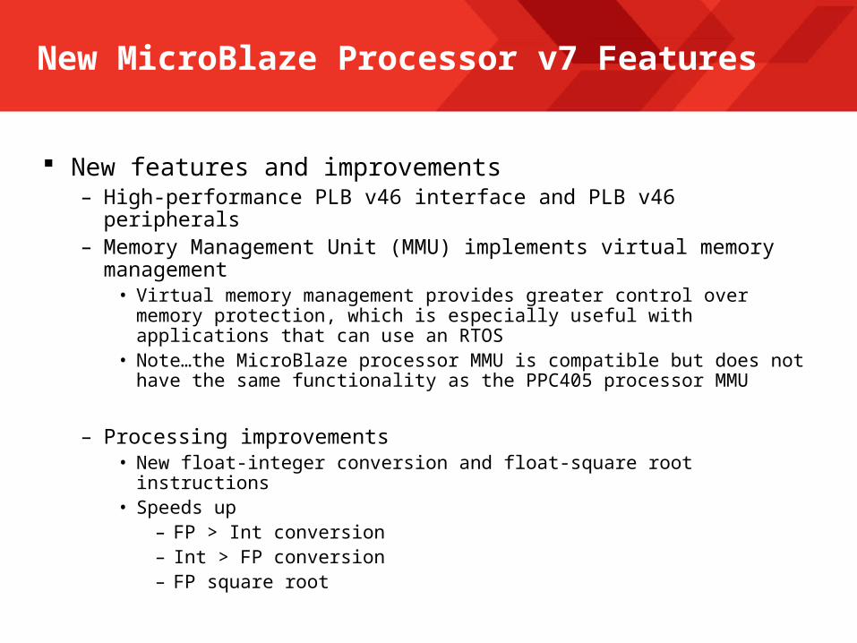
New MicroBlaze Processor v7 Features
New features and improvements– High-performance PLB v46 interface and PLB v46 peripherals– Memory Management Unit (MMU) implements virtual memory management
• Virtual memory management provides greater control over memory protection, which is especially useful with applications that can use an RTOS
• Note…the MicroBlaze processor MMU is compatible but does not have the same functionality as the PPC405 processor MMU
– Processing improvements• New float-integer conversion and float-square root instructions• Speeds up
– FP > Int conversion– Int > FP conversion– FP square root
© 2007 Xilinx, Inc. All Rights ReservedFPGA and ASIC Technology Comparison - 16
© 2007 Xilinx, Inc. All Rights ReservedFPGA and ASIC Technology Comparison - 16
© 2009 Xilinx, Inc. All Rights Reserved
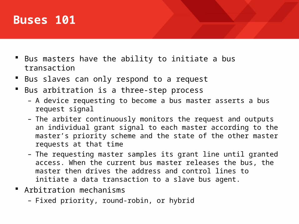
Buses 101
Bus masters have the ability to initiate a bus transaction Bus slaves can only respond to a request Bus arbitration is a three-step process
– A device requesting to become a bus master asserts a bus request signal– The arbiter continuously monitors the request and outputs an individual grant
signal to each master according to the master’s priority scheme and the state of the other master requests at that time
– The requesting master samples its grant line until granted access. When the current bus master releases the bus, the master then drives the address and control lines to initiate a data transaction to a slave bus agent.
Arbitration mechanisms– Fixed priority, round-robin, or hybrid
© 2007 Xilinx, Inc. All Rights ReservedFPGA and ASIC Technology Comparison - 17
© 2007 Xilinx, Inc. All Rights ReservedFPGA and ASIC Technology Comparison - 17
© 2009 Xilinx, Inc. All Rights Reserved
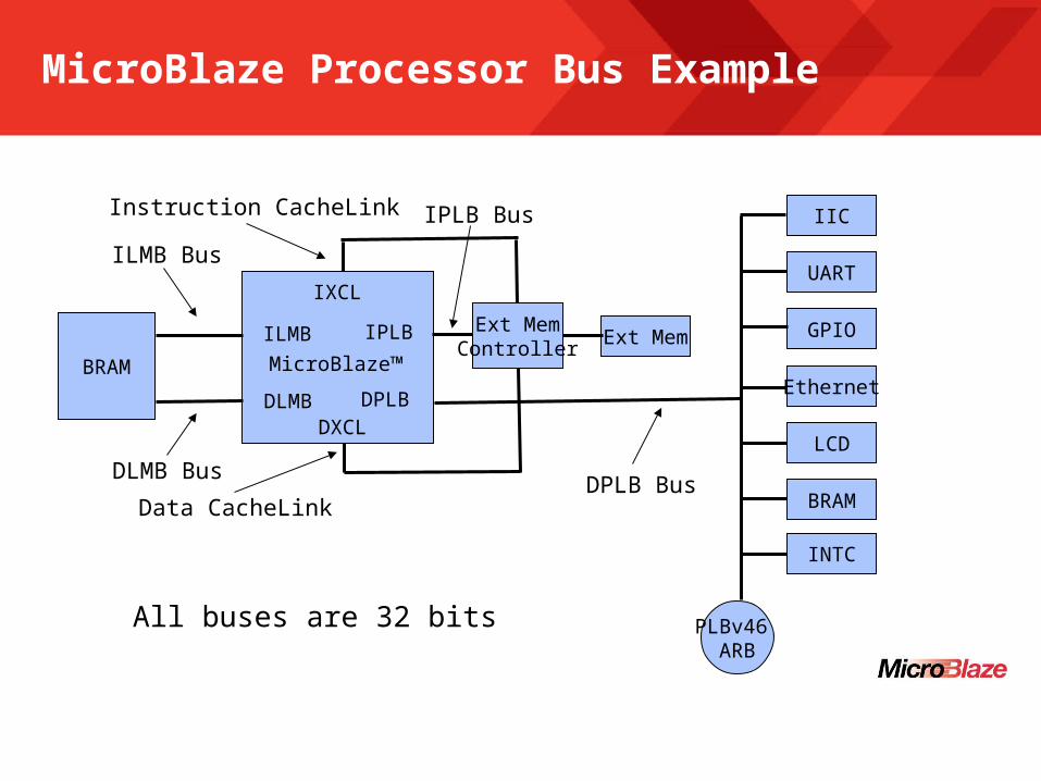
MicroBlaze Processor Bus Example
MicroBlaze™
DPLB
BRAM
DLMB
IIC
PLBv46 ARB
GPIO
UART
Ethernet
LCD
BRAM
INTC
IPLBILMB Ext Mem
ILMB Bus
DLMB BusDPLB Bus
IPLB Bus
All buses are 32 bits
IXCL
DXCL
Ext MemController
Instruction CacheLink
Data CacheLink
© 2007 Xilinx, Inc. All Rights ReservedFPGA and ASIC Technology Comparison - 18
© 2007 Xilinx, Inc. All Rights ReservedFPGA and ASIC Technology Comparison - 18
© 2009 Xilinx, Inc. All Rights Reserved
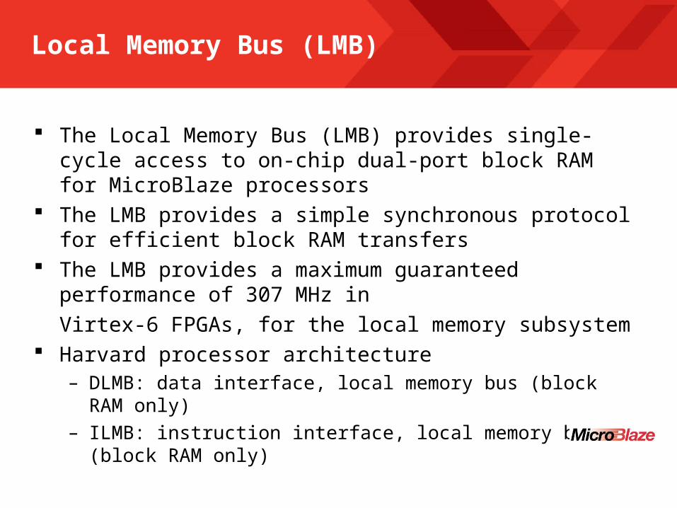
Local Memory Bus (LMB)
The Local Memory Bus (LMB) provides single-cycle access to on-chip dual-port block RAM for MicroBlaze processors
The LMB provides a simple synchronous protocol for efficient block RAM transfers
The LMB provides a maximum guaranteed performance of 307 MHz in Virtex-6 FPGAs, for the local memory subsystem
Harvard processor architecture– DLMB: data interface, local memory bus (block RAM only)– ILMB: instruction interface, local memory bus (block RAM only)
© 2007 Xilinx, Inc. All Rights ReservedFPGA and ASIC Technology Comparison - 19
© 2007 Xilinx, Inc. All Rights ReservedFPGA and ASIC Technology Comparison - 19
© 2009 Xilinx, Inc. All Rights Reserved
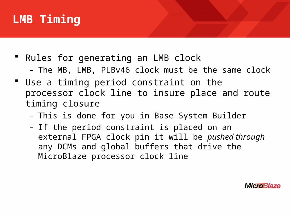
LMB Timing
Rules for generating an LMB clock – The MB, LMB, PLBv46 clock must be the same clock
Use a timing period constraint on the processor clock line to insure place and route timing closure – This is done for you in Base System Builder– If the period constraint is placed on an external FPGA clock pin it will be pushed
through any DCMs and global buffers that drive the MicroBlaze processor clock line
© 2007 Xilinx, Inc. All Rights ReservedFPGA and ASIC Technology Comparison - 20
© 2007 Xilinx, Inc. All Rights ReservedFPGA and ASIC Technology Comparison - 20
© 2009 Xilinx, Inc. All Rights Reserved
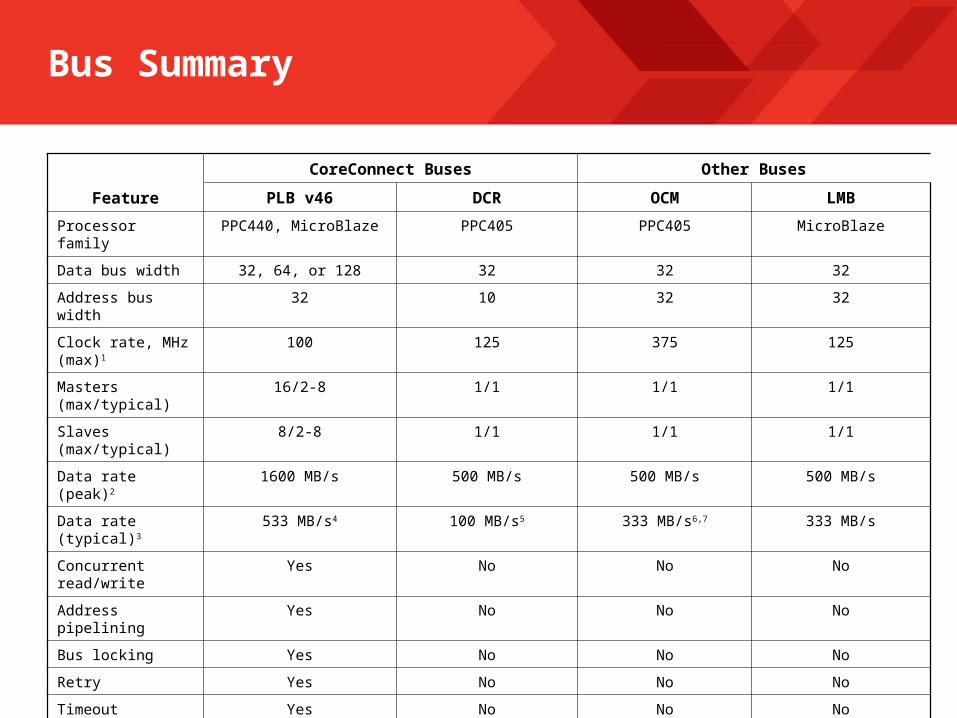
Bus Summary
Feature
CoreConnect Buses Other Buses
PLB v46 DCR OCM LMB
Processor family PPC440, MicroBlaze PPC405 PPC405 MicroBlaze
Data bus width 32, 64, or 128 32 32 32
Address bus width 32 10 32 32
Clock rate, MHz (max)1 100 125 375 125
Masters (max/typical) 16/2-8 1/1 1/1 1/1
Slaves (max/typical) 8/2-8 1/1 1/1 1/1
Data rate (peak)2 1600 MB/s 500 MB/s 500 MB/s 500 MB/s
Data rate (typical)3 533 MB/s4 100 MB/s5 333 MB/s6,7 333 MB/s
Concurrent read/write Yes No No No
Address pipelining Yes No No No
Bus locking Yes No No No
Retry Yes No No No
Timeout Yes No No No
Fixed/Variable Burst Yes No No No
Cache Fill Yes No No No
Target Word First Yes No No No
FPGA Resource Usage High Low Low Low
© 2007 Xilinx, Inc. All Rights ReservedFPGA and ASIC Technology Comparison - 21
© 2007 Xilinx, Inc. All Rights ReservedFPGA and ASIC Technology Comparison - 21
© 2009 Xilinx, Inc. All Rights Reserved
MicroBlaze Processor-Based Embedded Design
MicroBlaze32-Bit RISC Core
UARTMemory
Controller
Off-ChipMemory
FLASH/SRAM/DDR2
Fast Simplex Link
0,1….15
CustomFunctions
CustomFunctions
BRAM Local Memory
BusD-CacheBRAM
I-CacheBRAM
Possible inVirtex-5 FXT
CacheLink
PLB v46
MPLB
PowerPC405 Core
Dedicated Hard IP
PowerPC405 CorePowerPC440 Core
EMACHi-Speed
Peripheral
SPLB
PLB v46
Off-ChipDDR2
FSL Channels
© 2007 Xilinx, Inc. All Rights ReservedFPGA and ASIC Technology Comparison - 22
© 2007 Xilinx, Inc. All Rights ReservedFPGA and ASIC Technology Comparison - 22
© 2009 Xilinx, Inc. All Rights Reserved
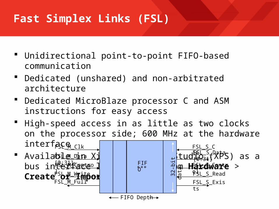
Fast Simplex Links (FSL)
Unidirectional point-to-point FIFO-based communication Dedicated (unshared) and non-arbitrated architecture Dedicated MicroBlaze processor C and ASM instructions for easy access High-speed access in as little as two clocks on the processor side; 600 MHz
at the hardware interface Available in Xilinx Platform Studio (XPS) as a bus interface library core from
Hardware > Create or Import Peripheral
FSL_M_Clk
FSL_M_Data [0:31]
FSL_M_Control
FSL_M_WriteFSL_M_Full
FSL_S_ClkFSL_S_Data [0:31]
FSL_S_Control
FSL_S_Read
FSL_S_Exists
FIFO
32-
bit d
ata
FIFO Depth
© 2007 Xilinx, Inc. All Rights ReservedFPGA and ASIC Technology Comparison - 23
© 2007 Xilinx, Inc. All Rights ReservedFPGA and ASIC Technology Comparison - 23
© 2009 Xilinx, Inc. All Rights Reserved
FSL Advantages
Simple, fast, and easy to use Clock speed is not slowed down by new hardware FSL is faster than a bus interface
– Saves clock cycles No arbitration/address decode/acknowledge cycles Decoupled data clock from CPU allows for asynchronous operation Minimal FPGA fabric overhead MicroBlaze processor v7 allows for up to 16 parallel FSL channels
PROPERTIESOn passing, 'Finish' button: Goes to Next SlideOn failing, 'Finish' button: Goes to Next SlideAllow user to leave quiz: After user has completed quizUser may view slides after quiz: At any timeUser may attempt quiz: Unlimited times
© 2007 Xilinx, Inc. All Rights ReservedFPGA and ASIC Technology Comparison - 25
© 2007 Xilinx, Inc. All Rights ReservedFPGA and ASIC Technology Comparison - 25
© 2009 Xilinx, Inc. All Rights Reserved
Hardware Overview PPC 440 Base System Builder Summary
Lessons
© 2007 Xilinx, Inc. All Rights ReservedFPGA and ASIC Technology Comparison - 26
© 2007 Xilinx, Inc. All Rights ReservedFPGA and ASIC Technology Comparison - 26
© 2009 Xilinx, Inc. All Rights Reserved
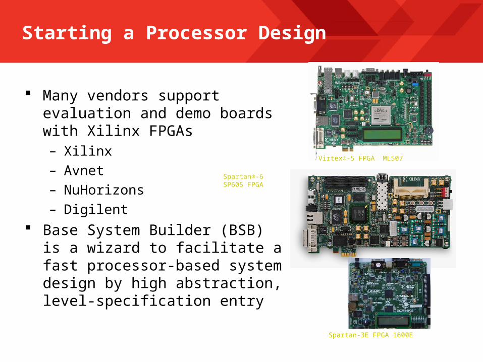
Many vendors support evaluation and demo boards with Xilinx FPGAs– Xilinx– Avnet– NuHorizons– Digilent
Base System Builder (BSB) is a wizard to facilitate a fast processor-based system design by high abstraction, level-specification entry
Starting a Processor Design
Virtex®-5 FPGA ML507
Spartan-3E FPGA 1600E
Spartan®-6 SP605 FPGA
© 2007 Xilinx, Inc. All Rights ReservedFPGA and ASIC Technology Comparison - 27
© 2007 Xilinx, Inc. All Rights ReservedFPGA and ASIC Technology Comparison - 27
© 2009 Xilinx, Inc. All Rights Reserved
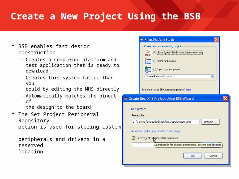
Create a New Project Using the BSB
BSB enables fast design construction– Creates a completed platform and
test application that is ready to download
– Creates this system faster than you could by editing the MHS directly
– Automatically matches the pinout of the design to the board
The Set Project Peripheral Repository option is used for storing custom peripherals and drivers in a reserved location
© 2007 Xilinx, Inc. All Rights ReservedFPGA and ASIC Technology Comparison - 28
© 2007 Xilinx, Inc. All Rights ReservedFPGA and ASIC Technology Comparison - 28
© 2009 Xilinx, Inc. All Rights Reserved
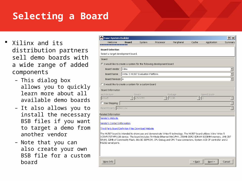
Selecting a Board
Xilinx and its distribution partners sell demo boards with a wide range of added components– This dialog box allows you
to quickly learn more about all available demo boards
– It also allows you to install the necessary BSB files if you want to target a demo from another vendor
– Note that you can also create your own BSB file for a custom board
© 2007 Xilinx, Inc. All Rights ReservedFPGA and ASIC Technology Comparison - 29
© 2007 Xilinx, Inc. All Rights ReservedFPGA and ASIC Technology Comparison - 29
© 2009 Xilinx, Inc. All Rights Reserved
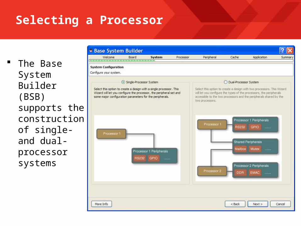
Selecting a Processor
The Base System Builder (BSB)supports the construction of single- and dual-processor systems

© 2007 Xilinx, Inc. All Rights ReservedFPGA and ASIC Technology Comparison - 30
© 2007 Xilinx, Inc. All Rights ReservedFPGA and ASIC Technology Comparison - 30
© 2009 Xilinx, Inc. All Rights Reserved
Configuring the Processor
Processor clock frequency is the clock rate connected directly to the processor
Bus clock frequency is the clock rate of all bus peripherals in the system
These selections will automatically customize the clock generator module
The appropriate debug interface is added automatically
© 2007 Xilinx, Inc. All Rights ReservedFPGA and ASIC Technology Comparison - 31
© 2007 Xilinx, Inc. All Rights ReservedFPGA and ASIC Technology Comparison - 31
© 2009 Xilinx, Inc. All Rights Reserved
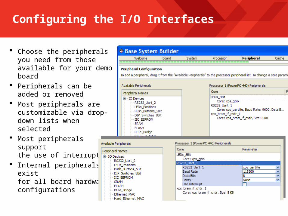
Configuring the I/O Interfaces
Choose the peripherals you need from those available for your demo board
Peripherals can be added or removed
Most peripherals are customizable via drop-down lists when selected
Most peripherals support the use of interrupts
Internal peripherals exist for all board hardware configurations
© 2007 Xilinx, Inc. All Rights ReservedFPGA and ASIC Technology Comparison - 32
© 2007 Xilinx, Inc. All Rights ReservedFPGA and ASIC Technology Comparison - 32
© 2009 Xilinx, Inc. All Rights Reserved
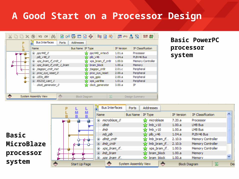
A Good Start on a Processor Design
Basic PowerPC processor system
Basic MicroBlaze processor system

© 2007 Xilinx, Inc. All Rights ReservedFPGA and ASIC Technology Comparison - 33
© 2007 Xilinx, Inc. All Rights ReservedFPGA and ASIC Technology Comparison - 33
© 2009 Xilinx, Inc. All Rights Reserved
Hardware Overview MicroBlaze Base System Builder Summary
Lessons
PROPERTIESOn passing, 'Finish' button: Goes to Next SlideOn failing, 'Finish' button: Goes to Next SlideAllow user to leave quiz: After user has completed quizUser may view slides after quiz: At any timeUser may attempt quiz: Unlimited times
© 2007 Xilinx, Inc. All Rights ReservedFPGA and ASIC Technology Comparison - 35
© 2007 Xilinx, Inc. All Rights ReservedFPGA and ASIC Technology Comparison - 35
© 2009 Xilinx, Inc. All Rights Reserved
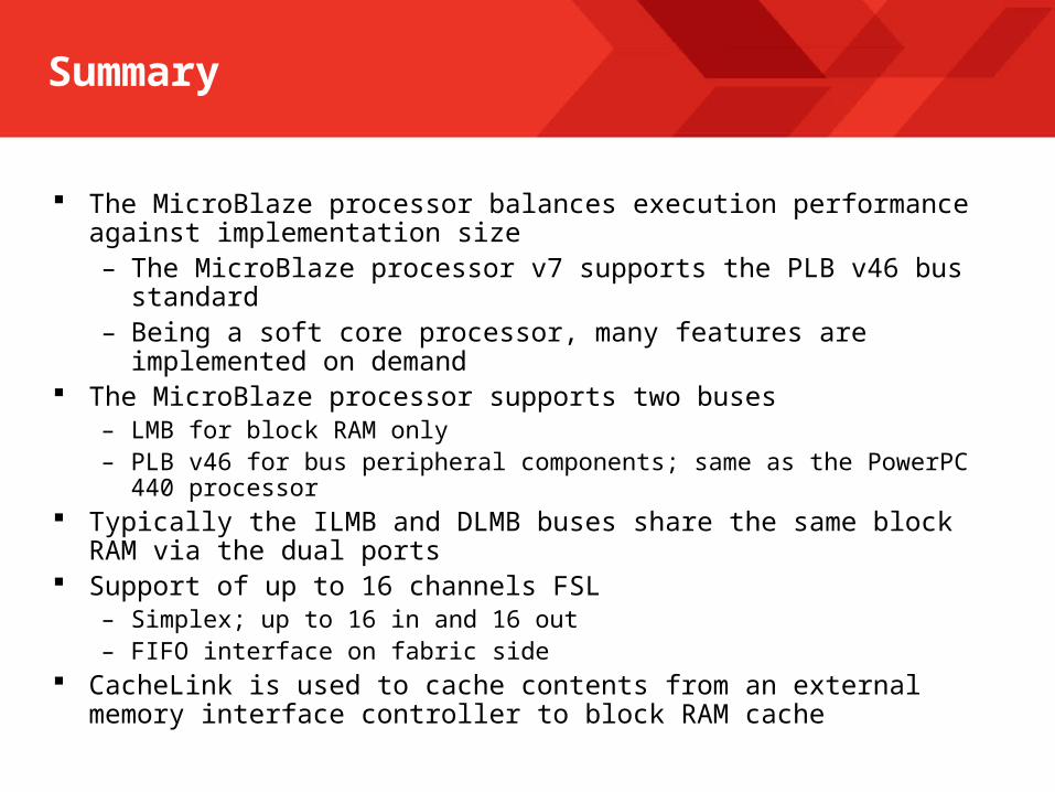
Summary
The MicroBlaze processor balances execution performance against implementation size– The MicroBlaze processor v7 supports the PLB v46 bus standard– Being a soft core processor, many features are implemented on demand
The MicroBlaze processor supports two buses– LMB for block RAM only– PLB v46 for bus peripheral components; same as the PowerPC 440 processor
Typically the ILMB and DLMB buses share the same block RAM via the dual ports Support of up to 16 channels FSL
– Simplex; up to 16 in and 16 out– FIFO interface on fabric side
CacheLink is used to cache contents from an external memory interface controller to block RAM cache
© 2007 Xilinx, Inc. All Rights ReservedFPGA and ASIC Technology Comparison - 36
© 2007 Xilinx, Inc. All Rights ReservedFPGA and ASIC Technology Comparison - 36
© 2009 Xilinx, Inc. All Rights Reserved
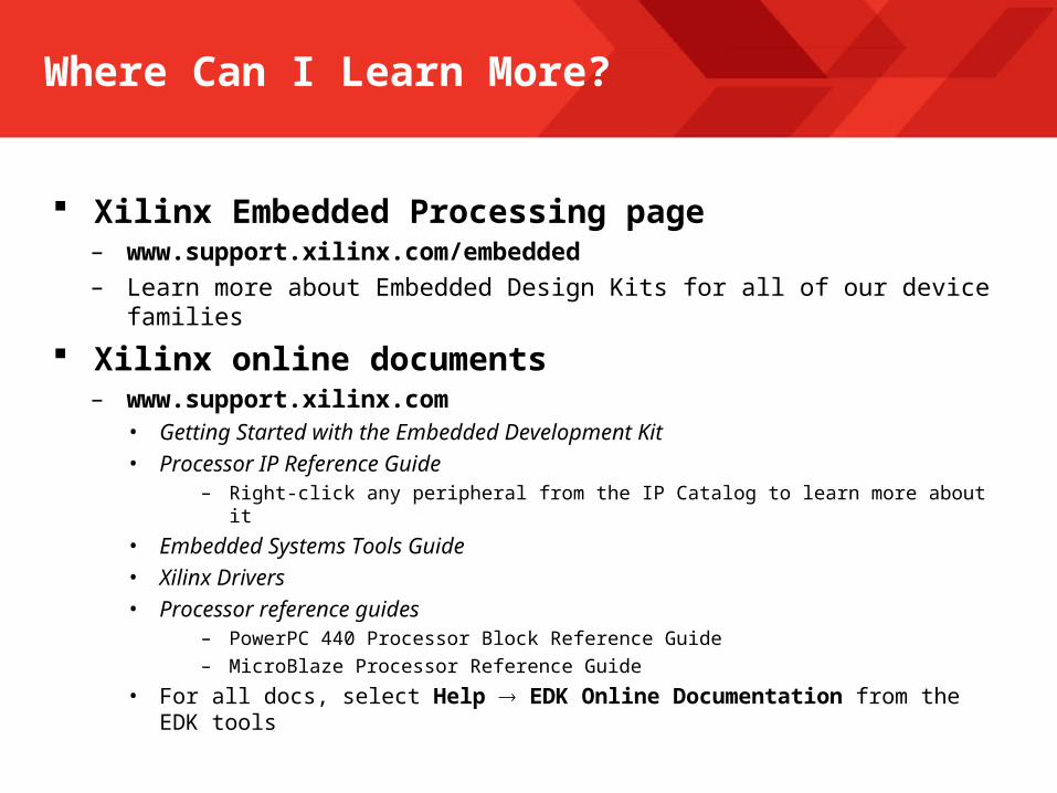
Where Can I Learn More?
Xilinx Embedded Processing page– www.support.xilinx.com/embedded– Learn more about Embedded Design Kits for all of our device families
Xilinx online documents – www.support.xilinx.com
• Getting Started with the Embedded Development Kit• Processor IP Reference Guide
– Right-click any peripheral from the IP Catalog to learn more about it• Embedded Systems Tools Guide• Xilinx Drivers• Processor reference guides
– PowerPC 440 Processor Block Reference Guide– MicroBlaze Processor Reference Guide
• For all docs, select Help EDK Online Documentation from the EDK tools
© 2007 Xilinx, Inc. All Rights ReservedFPGA and ASIC Technology Comparison - 37
© 2007 Xilinx, Inc. All Rights ReservedFPGA and ASIC Technology Comparison - 37
© 2009 Xilinx, Inc. All Rights Reserved
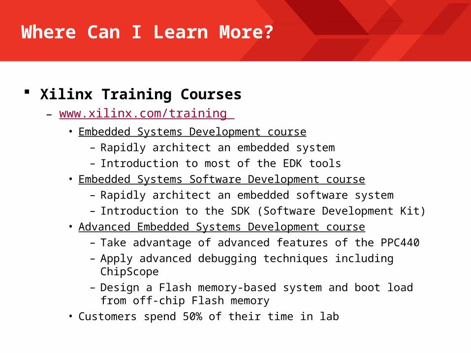
Where Can I Learn More?
Xilinx Training Courses– www.xilinx.com/training
• Embedded Systems Development course– Rapidly architect an embedded system– Introduction to most of the EDK tools
• Embedded Systems Software Development course– Rapidly architect an embedded software system– Introduction to the SDK (Software Development Kit)
• Advanced Embedded Systems Development course– Take advantage of advanced features of the PPC440– Apply advanced debugging techniques including ChipScope– Design a Flash memory-based system and boot load from off-chip Flash
memory• Customers spend 50% of their time in lab

© 2007 Xilinx, Inc. All Rights ReservedFPGA and ASIC Technology Comparison - 38
© 2007 Xilinx, Inc. All Rights ReservedFPGA and ASIC Technology Comparison - 38
© 2009 Xilinx, Inc. All Rights Reserved
What’s Next?
Provide your Feedback for this Course Return to the Course Details page View all Recorded eLearning Courses View all Instructor-led Training Courses Download PowerPoint with Transcripts Download Transcripts in MS Word Format To Download these files please hold the Ctrl key on your keyboard and Click the link
Related Video Courses– Embedded Design with the PPC 440– Embedded Design with the Xilinx Embedded Developer Kit
© 2007 Xilinx, Inc. All Rights ReservedFPGA and ASIC Technology Comparison - 39
© 2007 Xilinx, Inc. All Rights ReservedFPGA and ASIC Technology Comparison - 39
© 2009 Xilinx, Inc. All Rights Reserved
Xilinx is disclosing this Document and Intellectual Propery (hereinafter “the Design”) to you for use in the development of designs to operate on, or interface with Xilinx FPGAs. Except as stated herein, none of the Design may be copied, reproduced, distributed, republished, downloaded, displayed, posted, or transmitted in any form or by any means including, but not limited to, electronic, mechanical, photocopying, recording, or otherwise, without the prior written consent of Xilinx. Any unauthorized use of the Design may violate copyright laws, trademark laws, the laws of privacy and publicity, and communications regulations and statutes.
Xilinx does not assume any liability arising out of the application or use of the Design; nor does Xilinx convey any license under its patents, copyrights, or any rights of others. You are responsible for obtaining any rights you may require for your use or implementation of the Design. Xilinx reserves the right to make changes, at any time, to the Design as deemed desirable in the sole discretion of Xilinx. Xilinx assumes no obligation to correct any errors contained herein or to advise you of any correction if such be made. Xilinx will not assume any liability for the accuracy or correctness of any engineering or technical support or assistance provided to you in connection with the Design.
THE DESIGN IS PROVIDED “AS IS" WITH ALL FAULTS, AND THE ENTIRE RISK AS TO ITS FUNCTION AND IMPLEMENTATION IS WITH YOU. YOU ACKNOWLEDGE AND AGREE THAT YOU HAVE NOT RELIED ON ANY ORAL OR WRITTEN INFORMATION OR ADVICE, WHETHER GIVEN BY XILINX, OR ITS AGENTS OR EMPLOYEES. XILINX MAKES NO OTHER WARRANTIES, WHETHER EXPRESS, IMPLIED, OR STATUTORY, REGARDING THE DESIGN, INCLUDING ANY WARRANTIES OF MERCHANTABILITY, FITNESS FOR A PARTICULAR PURPOSE, TITLE, AND NONINFRINGEMENT OF THIRD-PARTY RIGHTS.
IN NO EVENT WILL XILINX BE LIABLE FOR ANY CONSEQUENTIAL, INDIRECT, EXEMPLARY, SPECIAL, OR INCIDENTAL DAMAGES, INCLUDING ANY LOST DATA AND LOST PROFITS, ARISING FROM OR RELATING TO YOUR USE OF THE DESIGN, EVEN IF YOU HAVE BEEN ADVISED OF THE POSSIBILITY OF SUCH DAMAGES. THE TOTAL CUMULATIVE LIABILITY OF XILINX IN CONNECTION WITH YOUR USE OF THE DESIGN, WHETHER IN CONTRACT OR TORT OR OTHERWISE, WILL IN NO EVENT EXCEED THE AMOUNT OF FEES PAID BY YOU TO XILINX HEREUNDER FOR USE OF THE DESIGN. YOU ACKNOWLEDGE THAT THE FEES, IF ANY, REFLECT THE ALLOCATION OF RISK SET FORTH IN THIS AGREEMENT AND THAT XILINX WOULD NOT MAKE AVAILABLE THE DESIGN TO YOU WITHOUT THESE LIMITATIONS OF LIABILITY.
The Design is not designed or intended for use in the development of on-line control equipment in hazardous environments requiring fail-safe controls, such as in the operation of nuclear facilities, aircraft navigation or communications systems, air traffic control, life support, or weapons systems (“High-Risk Applications”). Xilinx specifically disclaims any express or implied warranties of fitness for such High-Risk Applications. You represent that use of the Design in such High-Risk Applications is fully at your risk.
© 2009 Xilinx, Inc. All rights reserved. XILINX, the Xilinx logo, and other designated brands included herein are trademarks of Xilinx, Inc. All other trademarks are the property of their respective owners.
Trademark Information