Embed Size (px)
Citation preview

Skyworks Solutions, Inc. Proprietary Information 1
End-to-End Design and Simulation of Handset Modules
Pete Zampardi and Hongxiao Shao Skyworks Solutions, Inc.

Skyworks Solutions, Inc. Proprietary Information 2
Research vs. Production Design Flows
Research Design Flow
Work?
Simulate
Fabricate
Test
Apply for Follow-on
Ask for More
Funding
Yes
No
Work?
Simulate
Fabricate
Test
Re-Tune
Repeat 50 Million
Times
No
Yes
Production Design Flow

Skyworks Solutions, Inc. Proprietary Information 3
• Simulation Philosophy • What Does a Handset Amplifier Design Look Like? • Example Design Flows
– GSM (Controller + PA) – WCDMA (Bias/Logic Integrated with PA)
• Design Automation and Modeling Requirements/Strategy to Support This Flow
• Modeling Approach – Device Models – Inductor Tool – Thermal Considerations – Circuit Level “Modeling” – Laminates – Man Does Not Live by GaAs Die Alone…
• Conclusions
Outline

Skyworks Solutions, Inc. Proprietary Information 4
Modeling/Design Philosophy
• Goal of Modeling (for PA) is to Get Designer on the Green – Compact Models are the Drivers, Irons, and Wedges – Correlation of Lab and Simulation Benches is like “reading the green” – Behavioral Models could be the Putter
• Modeling VARIATION of the Process is More Important than Modeling a “Hero Device” – Variation is Important for Yield and System Performance
• Use Best Available Software for Each Piece, Glue Together with Custom Solutions
What are the Expectations?
Goal of Simulation is to Get Close as Fast as Possible, Predict Trends
The time needed for measuring a PAM with Pout sweeping from -5 to + 28 dBm (1dBm/step) and three frequencies, plus changing one SMT component was about 1500 sec. (V. Ho)

Skyworks Solutions, Inc. Proprietary Information 5
What Does a Handset Amplifier Design Look Like? HINT: NOT MADE OF DISCRETES
Control/Logic IC
Substrate and Assembly
Power Amp IC
Components SMT, Filter, etc
Power Amp Product
WCDMA Usually Combine These
On-chip
Glasbrener Breaking EDA Barriers RFIC Panel 2002
Simulation: DC, Trans., S-par and HB
Layout: GDSII
EM Simulation Layout: Gerber
Simulation: DC, Trans., S-par and HB
Layout: GDSII
Simulation: DC, Trans. S-par and HB
Skyworks Solutions, Inc. Proprietary Information 6
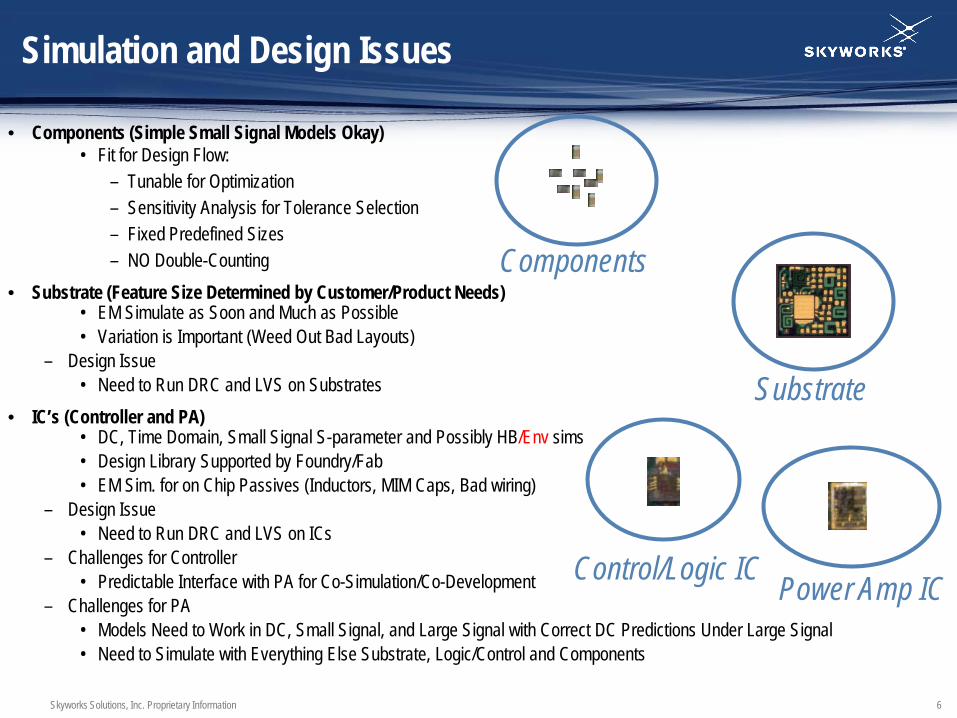
Simulation and Design Issues
• Components (Simple Small Signal Models Okay) • Fit for Design Flow:
– Tunable for Optimization – Sensitivity Analysis for Tolerance Selection – Fixed Predefined Sizes – NO Double-Counting
• Substrate (Feature Size Determined by Customer/Product Needs) • EM Simulate as Soon and Much as Possible • Variation is Important (Weed Out Bad Layouts)
– Design Issue • Need to Run DRC and LVS on Substrates
• IC’s (Controller and PA) • DC, Time Domain, Small Signal S-parameter and Possibly HB/Env sims • Design Library Supported by Foundry/Fab • EM Sim. for on Chip Passives (Inductors, MIM Caps, Bad wiring)
– Design Issue • Need to Run DRC and LVS on ICs
– Challenges for Controller • Predictable Interface with PA for Co-Simulation/Co-Development
– Challenges for PA • Models Need to Work in DC, Small Signal, and Large Signal with Correct DC Predictions Under Large Signal • Need to Simulate with Everything Else Substrate, Logic/Control and Components
Components
Substrate
Control/Logic IC Power Amp IC

Skyworks Solutions, Inc. Proprietary Information 7
PAM/FEM Design/Simulation Flow
Customized and Integrated Commercial and Home Grown EDA and other Application Software Tools
Process Design Kit Device Symbols Device Models Device Layout DRC, LVS Rule Files
IC-Package Link Bonding Diagrams Geom/S-Param Etc.
Package Libraries Discrete Component Vendor Models Package Model
Standard root Compatible with Tech Parallel Dev Teams Version Control IP Share/Reuse
Tools for root /root/$projID gen project Rev project Lock Release to Mask
Hierarchical Schematic Test Bench with Pkg/SMT Full Chip(s) Block in Design
Physical Design Schematic Driven Layout Layout Editor IC/Block in Design
Physical Verification Design Rule Check IC/Reticle Level IC/Block in Design
Post Layout Verification Layout vs. Schematic Parasitic Extraction Re-Sim with LPE
OK to Mask
Netlist for Pkg/Brd Physical Design
IC Footprint
Package/Board/Module Physical Design
Bill of Materials
Memory/Disk based DRC
OK to Tapeout
Bloc
k Lev
el Sy
stem
Per
form
ance
Bud
get A
nalys
is an
d Pa
rtitio
n
Man Cntl
Technology IP Product IP
Design Environment
Behavioral Models Could Be Effective Blocks Not Being Implemented

Skyworks Solutions, Inc. Proprietary Information 8
IC Centric Design Flow – Real Example Chips
Control and Bias Chip GaAs HBT PA Chip Power Detector Switch Chip Diplexer
Packages Embedded devices Discrete MCM
Multiple Process Technologies (Multi-Chip) ICs – Active/Passive Device Models, Interconnect/Inductor Modeling Package – Bond wire/Bump, SMT, Embedded Devices, Package Passive Modeling
pHEMT Switch Chip GaAs IC + Wire bond + Package (EM/Meas.) CMOS Chip CMOS IC + Wire bond + Discrete Components GaAs HBT Power Amp Chip GaAs IC + CMOS IC (at circuit or behavior level) + Wire bond + SMT + Package (EM/Meas.)
Design Electrical Design Physical Constraints (IC/Package) Thermal Management Part Tuning

Skyworks Solutions, Inc. Proprietary Information 9
GaAs HBT PA / PHEMT Switch Design Flow
Design, Analysis, and Simulation
MMIC Schematic
Preliminary MCM Schematic
Test Bench Schematic
EM Simulation HBT Models
Package Models SMT, BW, Laminate
MMIC Netlist PA MMIC Layout
HBT Layout Library, DRC
Rule Deck
Si Models
Models for supplies, stimuli, measurement, etc.
HBT Mask Generation
Die Symbol for MCM Layout
Die Symbol for MCM
Schematic
LVS
HBT PA Design Flow
Hierarchical Schematic
.die file
Simulation Bench
Skyworks Solutions, Inc. Proprietary Information 10
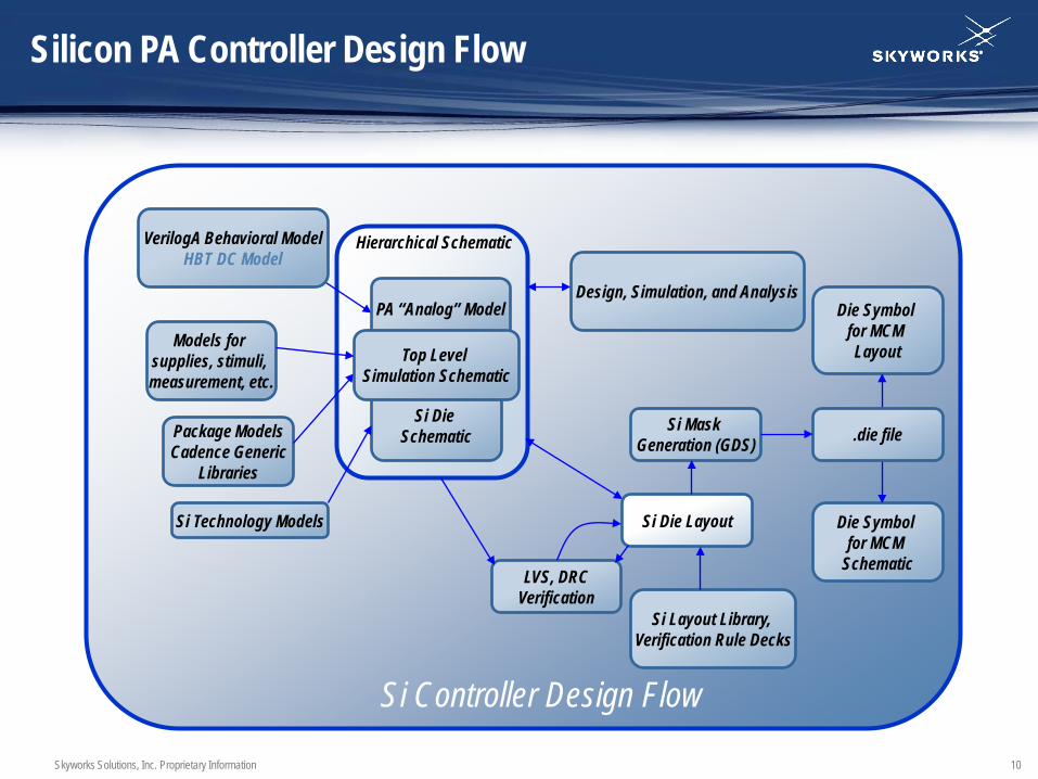
Silicon PA Controller Design Flow
Design, Simulation, and Analysis
Si Die Schematic Package Models
Cadence Generic Libraries
Si Die Layout
Si Layout Library, Verification Rule Decks
Si Technology Models
Models for supplies, stimuli, measurement, etc.
Si Mask Generation (GDS)
Die Symbol for MCM Layout
Die Symbol for MCM
Schematic LVS, DRC
Verification
Si Controller Design Flow
Hierarchical Schematic
PA “Analog” Model
Top Level Simulation Schematic
VerilogA Behavioral Model HBT DC Model
.die file

Skyworks Solutions, Inc. Proprietary Information 11
MCM Design Flow
Design, Analysis, and Simulation
MMIC Schematic
Preliminary MCM Schematic
Test Bench Schematic
EM Simulation
MCM MMIC Netlist MCM Layout
MCM Package Library
Die Symbol for MCM Layout
Die Symbol for MCM
Schematic
Wirebond Diagram
MCM Design Flow
Hierarchical Schematic From HBT / pHEMT Flow
.die file
MCM Package Level
Schematic Assembly Diagram
PCB Fab Drawing
Prototype BOM Text File Manipulation and Updates
BOM Generation
(1st time only)
Tuning, Alternate Component Eval, …
DC/AC Simulations to Verify Functionality RFDE Dynamic Link
Required for Si
MCM Schematic pdf
DMS
Skyworks Solutions, Inc. Proprietary Information 12
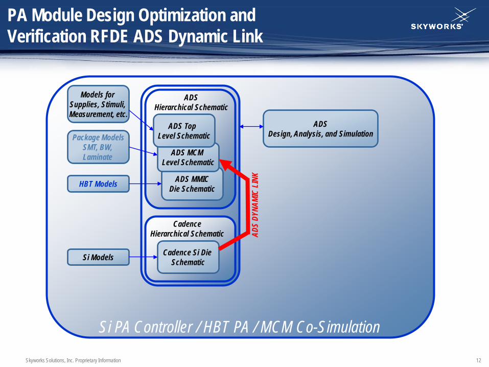
PA Module Design Optimization and Verification RFDE ADS Dynamic Link
ADS Design, Analysis, and Simulation
ADS MMIC Die Schematic
Package Models SMT, BW, Laminate
HBT Models
Models for Supplies, Stimuli, Measurement, etc.
Si PA Controller / HBT PA / MCM Co-Simulation
ADS Hierarchical Schematic
ADS MCM Level Schematic
ADS Top Level Schematic
Cadence Hierarchical Schematic
Si Models Cadence Si Die Schematic
ADS
DYNA
MIC
LINK

Skyworks Solutions, Inc. Proprietary Information 13
WCDMA Considerations
• Control Circuitry is ON-CHIP! – What the PA must do now is complicated
• Power Level Switching/Control • No Vref Bias Circuits
• Barrie Gilbert “RF design is 30% RF, 70% Bias Circuit” – Analog-mixed Signal Modeling Methodology Must be Applied
• Fully Scalable Device Models (for Optimization) • Statistical Simulations (Physically Based is Better)
• For High Volume Commercial Products, Yield Matters! – Statistics for Laminate Variations are Important (Not Just the Die)
Power Transistors
Power Transistors
PAs are More than “Just Two Transistors”
Most of the Chip is NOT Power Transistors

Skyworks Solutions, Inc. Proprietary Information 14
(W)CDMA PA/FEM Product Development Flow
Don’t Know Layout or off-chip stuff Understand Critical Blocks
With Estimated Tolerance to Parasitics
Provide Tools For 1st Order Best Guess of Things You’ll
Layout (Inductors/Caps) Know Variations
Simulate Stuff You Didn’t Know Earlier (Passives) For Production,
Statistical Simulation
Over Die Process And
Package Variation
Best Guess At Bond Wires
Scalable Device Models
IC Design Layout Co-Simulation
IC Design
Feasibility Study
Initial Simulation Schematic
Connectivity/ DC/Functionality
Layout
Module Design (Layout)
Extend Simulation MCM_RF
IC Layout Parasitic
EM Simulation
Co-Simulation IC+Module
Design for Manufacturing
(Par
tial)
Build
ing B
lock
Skyworks Solutions, Inc. Proprietary Information 15
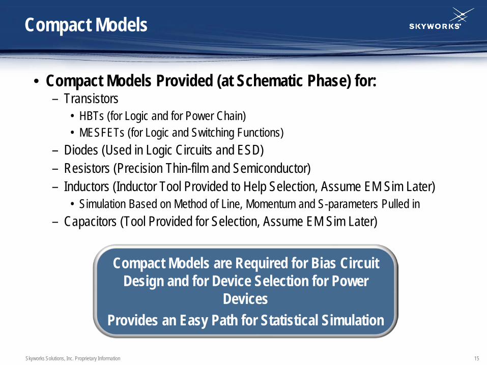
Compact Models
• Compact Models Provided (at Schematic Phase) for: – Transistors
• HBTs (for Logic and for Power Chain) • MESFETs (for Logic and Switching Functions)
– Diodes (Used in Logic Circuits and ESD) – Resistors (Precision Thin-film and Semiconductor) – Inductors (Inductor Tool Provided to Help Selection, Assume EM Sim Later)
• Simulation Based on Method of Line, Momentum and S-parameters Pulled in – Capacitors (Tool Provided for Selection, Assume EM Sim Later)
Compact Models are Required for Bias Circuit Design and for Device Selection for Power
Devices Provides an Easy Path for Statistical Simulation

Skyworks Solutions, Inc. Proprietary Information 16
Tech Devices Supported Wafers Meas.
Sites per Wafer Temperature # of Epi Statistics
GEN2 3 HBTs, 3 Diodes, Ls 1 1 HBT Only 1 No
GEN3 4 HBTs, 2 Diodes, Ls 1 1 HBT Only 1 No
GEN4 4 HBTs, 2 diodes, Ls, C’s
1 1 HBT/Diode 2 No
Current Scalable HBTs (Fixed-cell Rings,
Many Geometries of Straight Finger)
Scalable Diodes Rs, Ls, Cs
FETs for BiFET
Multiple 5 All 5 Yes
Evolution of Models at Skyworks
Ring Horseshoe
CEBEC (QSF) CEBEC (QSB_ALT)
QSB QSM
CEB, BEC, 1, 2, 4 finger
Increasing Number of Devices and Materials to Satisfy More Diverse Design Demands
Curve Fit
Physics Based
Zampardi, CMRF 2007
Physics-Based Scalable Approach Makes This a Tractable Problem

Skyworks Solutions, Inc. Proprietary Information 17
Inductor Tool Customized ADS
Enter TW, S, N, ID
Calculator outputs L, Q
Select inductor type, frequency
Kwok, Mantech 2008
Selector Mode
Press ‘Select’ to place instance in schematic
Specify required L, Q, layout area
Calculator Mode

Skyworks Solutions, Inc. Proprietary Information 18
Thermal Approaches/Considerations
• Maximum Junction Temperature Simulations (Reliability) • Thermal only Simulation (Okay if Properly Ballasted)
– Usually Compared/Validated Against IR Scans
• Thermal Coupling/Average Transistor Temperature (Electrical) – Bias Circuit – Array Design – Array to Array Interactions
• Complications – Inter-transistor interaction through interconnect/semiconductor/etc. – Thermal is Not Just Because of the Die: Laminate, Epoxy, Overmold, etc…
Absolute Temperature
Coupling
What Matters Thermally Depends on What You are Designing

Skyworks Solutions, Inc. Proprietary Information 19
The Simulation Problem
Circuit Simulation
Power Supply Voltages Power Dissipation Per Transistor
Die Layout
Placement of Transistors (Heat Sources)
Coupling Between Heat Sources
(Metal and Semiconductor)
Package Layout
Epoxy (Shape and Thickness) Placement of PTH
Coupling Between Heat Sources
(Metal and Laminate)
Thermal Simulations Require Inputs From All of These Electro-thermal Couples the Temperature Information Back into the Simulation
Compared to Digital/Analog Circuits, for a PA this Will Need to be Done Several Times at Any Given Power Since Electrical Parameters and Thermal Conductivities are Functions of Temperature
Much of the Packaging Information (Epoxy Thickness, Shape,
Die Placement, Die Thickness) is Difficult To collect Statistical Information on
PA Module/Phoneboard Cross-Section
PAM PHONEBOARD
Skyworks Solutions, Inc. Proprietary Information 20
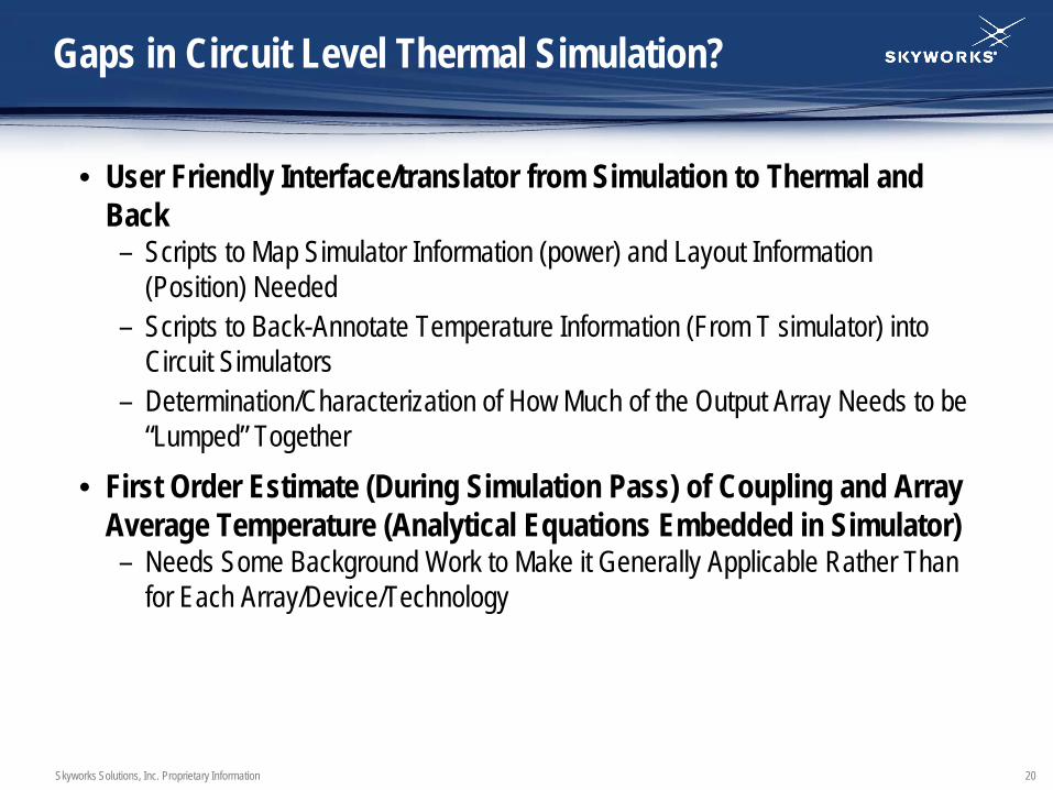
Gaps in Circuit Level Thermal Simulation?
• User Friendly Interface/translator from Simulation to Thermal and Back – Scripts to Map Simulator Information (power) and Layout Information
(Position) Needed – Scripts to Back-Annotate Temperature Information (From T simulator) into
Circuit Simulators – Determination/Characterization of How Much of the Output Array Needs to be
“Lumped” Together
• First Order Estimate (During Simulation Pass) of Coupling and Array Average Temperature (Analytical Equations Embedded in Simulator) – Needs Some Background Work to Make it Generally Applicable Rather Than
for Each Array/Device/Technology

Skyworks Solutions, Inc. Proprietary Information 21
-15 -10 -5 0 5 10 15-20 20
0
10
20
30
-10
40
RFpow er
Gai
n
gain
Pou
t
poutgainRFpower=Gain=17.317
-18.000
poutRFpower=Pout=31.425
18.000
-15 -10 -5 0 5 10 15-20 20
20
40
0
60
0.2
0.3
0.4
0.5
0.6
0.7
0.8
0.9
0.1
1.0
RFpow er
PA
E_C
PAEreal(Ic.i[::,0])
Icc
PAERFpower=PAE_C=58.930
18.000
IccRFpower=real(Ic.i[::,0])=0.638
18.000
RFpow er
-18.000
gain
17.317
RFpow er
18.000
pout
31.425
PAE
58.930
Icc
0.638
Temperature Simulations on Array
Simulation No. Description Gain Pout PAE 1 No T Rise 17.317 31.425 58.93 2 T Rise = 10 17.938 31.48 58.893 3 Avg T Rise = 2.1 17.456 31.439 58.926 4 Avg T Rise = 4.54 17.61 31.455 58.917 5 Avg T Rise = 7.27 17.755 31.473 58.9 6 Avg T Rise = 20.9 18.324 31.565 58.745 7 Hotspot Avg T=6.8 17.607 31.479 58.856
22 Transistor Array Optimal Load for All Qs at same temp Ballast and Pre-matched
Average Temperature is What Matters For Electrical Simulation
CMRF 2007

Skyworks Solutions, Inc. Proprietary Information 22
Array Parasitic Approaches (Teaching Designers to Fish)
Simple Multiplicity Factor Pro: Fast/Simple Con: Phase Error >8GHz
Lumped Element Pro: Fast Con: Layout Specific, Hard to Scale
EM Simulation Reduced Number of HBTs or All HBTs Pro: Easy to Do, No Modeler Required Con: Simulation Speed Bogs Down with Increased Transistor Count
Transmission Line: Pro: Moderate Speed, Scalable, Easy Con: Accurate Up to 12GHz

Skyworks Solutions, Inc. Proprietary Information 23
Load-Pull Power Sweep with Different EM Approaches
Gain Comparison
10
12
14
16
18
20
22
-15 -10 -5 0 5 10 15
Pin (dBm)
Gai
n (d
B)
Gain, measGain, EM-1HBTGain, EM-2HBTGain, EM-3HBTGain,EM--12HBTGain, Simple_MGain, TLMGain, Lumped
Pout Comparison
0
5
10
15
20
25
30
-15 -10 -5 0 5 10 15
Pin (dBm)
Pout
(dBm
)
Pout, measPout, EM-1HBTPout, EM-2HBTPout, EM-3HBTPout,EM-12HBTPout, Simple_MPout, TLMPout, Lumped
Ic Comparison
0
20
40
60
80
100
120
140
160
180
200
-15 -10 -5 0 5 10 15
Pin (dBm)
Ic (m
A)
Ic(mA), measIc(mA), EM-1HBTIc(mA), EM-2HBTIc(mA), EM-3HBTIc(mA),EM-12HBTIc(mA),simple_MIc(mA), TLMIc(mA), Lumped
• On-wafer LP measurement at freq=1.9GHz, Vc=3.4V, Ic=14.6mA
No Huge Differences Based on Approach!
EM Slightly Better Simple Approach Off at High Power

Skyworks Solutions, Inc. Proprietary Information 24
Statistical Simulation: All-In-One and Interactive
Yang, Microwave Journal, 2008

Skyworks Solutions, Inc. Proprietary Information 25
Statistics – Understand Expected Variation
Compared with measurement, PA circuit simulation shows good tracking of DOE variations.
Statistical Inputs: PCM Parameters from
Measured DOE Wafers
Power Sweep Performed

Skyworks Solutions, Inc. Proprietary Information 26
Statistics: Identify Issues and Improve Design!
-20 -10 0 10 20 30 40 50 60 70 80-30 85
25
26
27
28
29
30
31
32
24
33
Temperature (C)
dB(S
21)
m1
db(S 21) v s temp
m1indep(m1)=plot_vs(dB(S(2,1)), SP.temp)=29.12freq=836.5000MHz, doeIter=0
25.000
-20 -10 0 10 20 30 40 50 60 70 80-30 85
0.015
0.020
0.025
0.030
0.010
0.035
Temperature (C)
Icq1
(A
)
-20 -10 0 10 20 30 40 50 60 70 80-30 85
0.04
0.05
0.06
0.07
0.08
0.09
0.03
0.10
Temperature (C)
Icq2
(A
)
Performance Ranges (at 25C): dB(S21)(25.64 to 31.54)=5.9 Icq1(13 to 28)=15mA (79%) Icq2(44 to 90)=46mA (72%)
Performance Ranges (at 25C): dB(S21)(25.88 to 29.42)=3.5 Icq1(19 to 30)=11mA (46%) Icq2(35 to 53)=18mA (41%)
-20 -10 0 10 20 30 40 50 60 70 80-30 85
25
26
27
28
29
30
31
32
24
33
Temperature (C)
dB(S
21)
m1
db(S 21) v s temp
m1indep(m1)=plot_vs(dB(S(2,1)), SP.temp)=27.892freq=836.5000MHz, doeIter=969
25.000
-20
-10
0 10 20 30 40 50 60 70 80-30
85
0.015
0.020
0.025
0.030
0.010
0.035
Temperature (C)
Icq1
(A
)
-20
-10
0 10 20 30 40 50 60 70 80-30
85
0.04
0.05
0.06
0.07
0.08
0.09
0.03
0.10
Temperature (C)
Icq2
(A
)
dB(S21)
Icq1
Icq2
Variation Significantly Reduced!
BEFORE AFTER

Skyworks Solutions, Inc. Proprietary Information 27
Laminate DOE Simulation
• Batch Based Momentum Simulations on DOE states to capture the laminate process variations:
– Layer over Layer Misalignment – Geometry Size Variations – Dielectric and Layer Thickness Variations – Can Also Be Applied at Die Level
• After Completion of the Batch Based simulation, a Symbol is Generated to Enable the Passive Block, with DOE Analysis Results, to Simulator with Other Blocks at the Circuit Level
• Pareto charts in ADS Data Display is created once the circuit level DOE analysis is complete.
Portion of Output Match Symbol
in ADS schematic
7 laminate re-related variables are defined for DOE analysis
Layer over layer offset in X-axis L1 trace width
Assume SMT cap variation as follows: C = +/- 0.1 pF L = +/- 0.05 nH, R = +/- 0.1 Ohm

Skyworks Solutions, Inc. Proprietary Information 28
Issues for Behavioral Modeling
• We Use Multiple Materials to Address Diverse Product Needs = Nmaterial • Allow Different Unit Cells for Application = Ncells • Different Ballasting/Feedback For Different Designs = Nballast • Different Array Layouts/Size Requirements for Applications = Narray • Process Variation (Say a Few Parameters Will Multiply this by 2Nvariation)
Using Behavioral Models For Simulating Integrated PA Designs Creates an Intractable Problem!
arrayballastcellsmaterialModels NNNNN =
For FETs, This is an Easier Problem – Single Gate Length, Gate Width Scaling (by Adding Cells), No Ballasting. Process Variation is a Bigger Headache!

Skyworks Solutions, Inc. Proprietary Information 29
Where Does Behavioral Modeling Fit In?
• Designs Using Discrete Transistor Blocks • Not as Prevalent in Handset Designs Anymore but Used to be Common 10 year ago • Simple Behavioral Models of PA for Bias Design, and of Bias for PA Design (Usually
Implemented in VerilogA) • Package Centric Product Design (Re-use of Controller and/or PA Engines) • System Level Simulations (Still Issues with Statistics, but More Manageable) • If It Can Be Used to Improve Speed of Characterization • When the Technology is Not Well Understood
• Could Be Used as “Putter” Once Compact Models get You Close
• Things That Still Need to Be Ironed Out • Incorporation of Statistics • Memory Effects (especially thermal) • Validation that Insides of Black-Box are Independent of What Happens Outside

Skyworks Solutions, Inc. Proprietary Information 30
Conclusions
• Compact Models Provide a Greatest Leverage in Simulating Handset PAs, Especially Statistics • The Real Issues Facing PA Designers are Often Misunderstood
• Layout Parasitics • Thermal Impact on Electrical Performance • Stuff Besides Die is also Critical
• Behavioral Models are Useful at System/FEM Design Level and for Technologies that are not Well Understood. • Statistics are Critical, Even for Package and Embedded Passives
Skyworks Solutions, Inc. Proprietary Information 31
Acknowledgments
Mats Fredriksson Mike Glasbrener Kai Kwok Yingying Yang Juntao Hu Shing Li

Skyworks Solutions, Inc. Proprietary Information 32
References
M. Glasbrener, “Breaking EDA Barriers” 2002 IEEE MTT Panel Discussion R. Jos, “Future developments and technology options in Cellular Phone Power Amplifiers: from power amplifier to integrated RF front-end module”, BCTM Technical Digest, 2000, pp. 118-125 B. Gilbert, “Biasing techniques for RF/IF signal processing”, presented at the MEAD Lecture Series short-course lecture, UC Berkeley, CA,1987 P. Zampardi, “III-V HBT Modeling Issues and Future Directions”, CMRF 2004 Workshop, Montreal, Quebec, Canada K. Kwok, “Simple DOE-based inductor tool for design automation”, 2008 CS Mantech Conference, Paper 17.2 Y. Yang, “An Innovative and Integrated Approach to III-V Circuit Design”, Microwave Journal, September 2008, pp. 136-156

![A Markdown Interpreter for TeX · 2020. 9. 14. · 10if not modules then modules = { } end 11modules['markdown'] = metadata 1.1 Feedback PleaseusetheMarkdownprojectpageonGitHub4toreportbugsandsubmitfeature](https://img.pdfslide.net/doc/110x75/601f50554b07a239300d175e/a-markdown-interpreter-for-tex-2020-9-14-10if-not-modules-then-modules-.jpg)