Embed Size (px)
Citation preview

3940 IEEE TRANSACTIONS ON ELECTRON DEVICES, VOL. 58, NO. 11, NOVEMBER 2011
Endurance Characteristics of Amorphous-InGaZnOTransparent Flash Memory With Gold Nanocrystal
Storage LayerJaeman Jang, Jae Chul Park, Dongsik Kong, Dong Myong Kim, Member, IEEE, Jang-Sik Lee, Member, IEEE,
Byeong-Hyeok Sohn, Il Hwan Cho, Member, IEEE, and Dae Hwan Kim, Member, IEEE
Abstract—The amorphous indium–gallium–zinc-oxide(a-IGZO) thin-film transistor (TFT)-based nonvolatiletransparent Flash memory devices were fabricated withgold (Au) nanocrystal storage layer. The performance andthe reliability of transparent memory devices have beencharacterized by experiment and technology computer-aideddesign simulation. This memory device shows a large-enoughmemory window ∆V = 4.7 V at the program/erase (P/E)voltage VPGM/VERS = 35/ − 35 V for the P/E timeTPGM/TERS = 3/25 s. The memory window was kept almostthe same after 1050 P/E cycles; however, the center voltage of thememory window (VC ) was shifted in a negative direction. Thecycling effect was explained by the change in the density of states(DOS) and the acceptor-like interface-trap density DitA(E) inthe a-IGZO channel layer with increasing P/E cycles. The mainmechanism for the change in VC was found to be the acceleratedinjection of holes into the gate insulator due to the energy bandbending during the erase operation.
Index Terms—Amorphous indium–gallium–zinc-oxide(a-IGZO), density of states (DOS), nonvolatile memory, thin-filmtransistors (TFTs).
I. INTRODUCTION
R ECENTLY, a demand for transparent display applicationshas been increasing in various respects. Transparent elec-
tronics offers an opportunity to develop optoelectronic devicesfor “see-through” display technologies and other applications[1]. A key element to realize transparent circuits is a trans-parent thin-film transistor (TFT) [2]. Therefore, studies ontransparent oxide-TFTs have attracted considerable attention
Manuscript received June 9, 2011; revised July 21, 2011; acceptedAugust 2, 2011. Date of current version October 21, 2011. This work wassupported by the Mid-Career Researcher Program through the National Re-search Foundation grant funded by the Ministry of Education, Science, andTechnology under Grant 2009-0080344. The review of this paper was arrangedby Editor A. Schenk.
J. Jang, D. Kong, D. M. Kim, and D. H. Kim are with the School ofElectrical Engineering, Kookmin University, Seoul 136-702, Korea (e-mail:drlife@ kookmin.ac.kr).
J. C. Park is with Samsung Advanced Institute of Technology, Yongin 446-712, Korea.
J.-S. Lee is with the School of Advanced Materials Engineering, KookminUniversity, Seoul 136-702, Korea.
B.-H. Sohn is with the Department of Chemistry and the NANO SystemsInstitute, Seoul National University, Seoul 151-747, Korea.
I. H. Cho is with the Department of Electronic Engineering, MyongjiUniversity, Yongin 449-728, Korea.
Color versions of one or more of the figures in this paper are available onlineat http://ieeexplore.ieee.org.
Digital Object Identifier 10.1109/TED.2011.2164252
with respect to display applications because of their capabilityfor large-scale and low-cost fabrication at low temperature[3]–[5].
Among many types of transparent oxide semiconductors(TOSs), the indium–gallium-doped amorphous zinc oxide[amorphous indium–gallium–zinc-oxide (a-IGZO)] is one ofthe most promising TOSs and offers many advantages overconventional amorphous/polycrystalline silicon in terms of itshigh mobility, high aspect ratio, and low processing tempera-tures [6]–[10]. Most of the research in this field is focused onimproving the electrical properties of TFTs with a-IGZO filmsfor the active layer [11], [12].
Meanwhile, the nanocrystal charge trap memory is alsoexpected to be a promising next-generation storage device [13].Nanocrystal Flash memory devices have advantages over theconventional memory devices with improved flexibility in thedesign through a controllable state-of-the-art process formingnanocrystal arrays. In particular, by adopting a conductingmetal for nanocrystals, a metal nanocrystal memory has signif-icant advantages with higher density for charge storage nodes,stronger coupling with the conduction channel, a wide range ofavailable work function, and smaller energy perturbation due toa carrier confinement [13]–[15].
We also note that there is a new approach to implement atransparent nonvolatile Flash memory device with TOSs forvarious innovative applications [16]–[21]. This is because thesememory device cells can be easily integrated into the displaydevices. Specifically, nonvolatile memory devices based on a-IGZO TFTs can be applied to flexible electronic devices be-cause a-IGZO thin films can be synthesized at low temperature[18]–[21].
As a possible transparent nonvolatile memory in the next-generation, the nonvolatile nanocrystal Flash memory deviceshave been fabricated and characterized based on low-temperature-processed controlled gold (Au) nanocrystals as acharge storage layer and the a-IGZO film as an active layer [20],[21]. However, the memory characteristics of a-IGZO memorywith gold nanocrystals were introduced through previous works[20], [21]; the detailed analysis of reliability is not yet clarified.
In this paper, the endurance characteristics and physicalmechanisms of the Au nanocrystal-embedded a-IGZO trans-parent memory device was explained through the extractedphysical parameters of the a-IGZO active layer including thesubgap density of states (DOS) and the density of interface
0018-9383/$26.00 © 2011 IEEE

JANG et al.: ENDURANCE CHARACTERISTICS OF a-IGZO TRANSPARENT FLASH MEMORY 3941
Fig. 1. Device structure of the Au nanoparticle-embedded transparent a-IGZOTFT Flash memory. (a) Schematic top view; (b) cross-sectional view, A - A′;and (c) cross-sectional view, B - B′.
traps (Dit) by the multifrequency C–V method (MFM) andthe DOS-based amorphous oxide TFT simulations (DeAOTSs)[22], [23].
II. FABRICATION OF Au NANOCRYSTAL-EMBEDDED
a-IGZO TRANSPARENT MEMORY DEVICES
The three-dimensional structure of the Au nanocrystal-embedded a-IGZO-based transparent memory device with aninverted staggered type, which is the most commonly used forTFTs, is shown in Fig. 1. The memory device was fabricatedwith an a-IGZO channel and the Au nanocrystal storage layeron the glass substrate.
A brief fabrication procedure for the Au nanocrystal-embedded a-IGZO transparent memory devices is as follows.On a glass substrate, the first sputtered deposition at roomtemperature (RT) and the patterning of the molybdenum (Mo)gate are followed by plasma-enhanced chemical vapor de-
position (PECVD) of the blocking oxide (Tbot = 70 nm) at300 ◦C. In addition, the Au nanocrystal charge storage layerwas formed. The synthesis of the charge trapping layer has beenalready reported in detail elsewhere [24], [25]. In brief, Aunanocrystals were synthesized using polystyrene-block-poly(4-vinyl pyridine) purchased from Polymer Source, Inc. Au as ametallic nanocrystal was selected since it not only has a suitablework function (5.5 eV) for such applications but also exhibitsa low anneal temperature for nanocrystal formation, which isadvantageous to the quality of underlying SiO2 dielectrics.Combining advantages of both the metal nanocrystal and thehigh tunneling barrier, excellent data retention characteristicshave been achieved without yielding the programming effi-ciency. Then, 30-nm-thick tunneling oxide (Ttop = 30 nm) wasdeposited onto the storage layer by PECVD. The a-IGZO activelayer (Ga2O3 : In2O3 : ZnO = 2:2:1 at.%) is then sputtered bythe radio-frequency magnetron sputtering at RT in a mixedatmosphere of Ar/O2 (100:1 at standard cubic centimeters perminute) and patterned by the wet etch process with dilutedHF. For the formation of source/drain (S/D) electrodes, Mo issputtered at RT and then patterned by dry etching. After N2Oplasma treatment on the channel surface of the a-IGZO activelayer, a SiO2 passivation layer is continuously deposited at150 ◦C by PECVD without a vacuum break. Finally, annealingin the furnace at 250 ◦C is performed for 1 h in an N2
atmosphere.The structural parameters of the Au nanoparticle-embedded
transparent a-IGZO TFT Flash memory are designed to beWIGZO = 5 µm for the width of the region between the gateand the a-IGZO active, LIGZO = 15 µm for the length betweenthe S/D and the a-IGZO active, TIGZO = 60 nm for the thick-ness of the IGZO layer, LOV = 5 µm for the overlap betweenthe gate and the S/D, the nanocrystal density per unit area N =6.4 × 1010 cm−2, the diameter of nanocrystals D = 14 nm, andthe distance between the nanocrystals S = 30 nm, as indicatedin Fig. 1(a)–(c).
III. CHARACTERIZATION OF ENDURANCE IN THE AuNANOCRYSTAL-EMBEDDED a-IGZO
TRANSPARENT MEMORY
A. Program/Erase Operations
The operation of the Au nanocrystal-embedded a-IGZO-based transparent memory was experimentally verified. Theprogram/erase (P/E) characteristics are measured, and physi-cal mechanisms are investigated combining the energy banddiagrams.
Memory operations of the Au nanocrystal were experimen-tally verified applying the same program operation to a-IGZOTFT devices with and without the nanocrystal storage layerat the interface between the tunneling oxide and the insulat-ing oxide. Fig. 2 show the transfer characteristics of a-IGZOTFTs. The program was performed at the gate-to-source voltageVGS = 20 V and a stress time of 1 s keeping the source and thedrain grounded.
As shown in Fig. 2(a), the threshold voltage VT shift was notobserved in the a-IGZO TFT device without the Au nanocrystalstorage layer even after programming. For the a-IGZO TFT

3942 IEEE TRANSACTIONS ON ELECTRON DEVICES, VOL. 58, NO. 11, NOVEMBER 2011
Fig. 2. Transfer characteristics of the transparent memory device (a) withoutand (b) with the Au nanocrystal storage layer. The initial curve was measuredwithout a P/E operation. The program states were achieved by applying biasstresses of 20 V to the gate for 100 ms and 1 s.
device with the Au nanocrystal storage layer after the sameprogram condition, on the other hand, VT was clearly shifted by∆VT = 3 V in a positive direction, as shown in Fig. 2(b). It isclear that the Au nanocrystal layer works as a storage layer forthe transparent memory device implemented in a-IGZO TFTs.
B. Endurance Characteristics
Fig. 3 shows the endurance characteristics of the Aunanocrystal-embedded oxide TFT Flash memory device. Theprogram was performed at VPGM = 35 V for TPGM = 3 s,and the erase operation was performed at VERS = −35 V forTERS = 25 s under photonic illumination from the backlightunit. Fig. 3(a) shows that the programmed and erased VT
values were shifted with increasing the number of P/E cy-cles. The difference of the programmed and erased VT values(Memory window ∆V = 4.7 V) was maintained constant after1050 P/E cycles. The memory window was independent of theP/E cycles, as shown in Fig. 3(b).
However, the center voltage of the memory window (VC)was shifted by −12.7 V after repeated P/E cycles, and theshifted VT may cause errors during the READ operation. Thisphenomenon seems to be the same as the VT characteristicsof the negative-bias illumination stress effect in a-IGZO oxideTFTs [11], [12]. In this paper, the negative VT shift phenom-
Fig. 3. Endurance characteristics of Au nanocrystal-embedded a-IGZO trans-parent memory device. (a) Threshold voltage shift as a function of P/E statesand P/E cycling. (b) Memory window (∆V = VT_PGM − VT_ERS) changeas function of the number of P/E cycling.
enon with repeated P/E cycles is investigated by the extractionof DOS and Dit after P/E cycles.
C. Cycling-Dependent DOS and Dit in the a-IGZOActive Layer
The physical parameters including DOS and Dit were ex-tracted by the MFM combined with the DeAOTS [22], [23].
The measured C–V characteristics of the Au nanocrystal-embedded a-IGZO transparent Flash memory device are shownin Fig. 4. Fig. 4(a) and (b) show the frequency-dependent C–Vcharacteristics for the initial state before P/E cycling and after1050 P/E cycles. The C–V characteristics were measured atsmall-signal frequencies f = 10, 100, and 500 kHz for theMFM technique.
Fig. 5 shows the extracted subgap acceptor-like DOS gA(E)(in eV−1cm−3) of the a-IGZO active layer. Assuming an expo-nential distribution of the deep states, it can be modeled as
gA(E) = gDA(E)+gTA(E)
=NDA×exp(
E−EC
kTDA
)+NTA exp
(E−EC
kTTA
).
(1)
We note that four characteristic parameters NTA, NDA,kTTA, and kTDA in gA(E) are not fitting parameters butphysical and extractable parameters because they can be exper-imentally extracted [26]–[28].

JANG et al.: ENDURANCE CHARACTERISTICS OF a-IGZO TRANSPARENT FLASH MEMORY 3943
Fig. 4. Frequency-dependent C–V characteristics measured by using LCRmeter (HP 4284 A). (a) Before P/E cycling. (b) After P/E 1050 cycling.
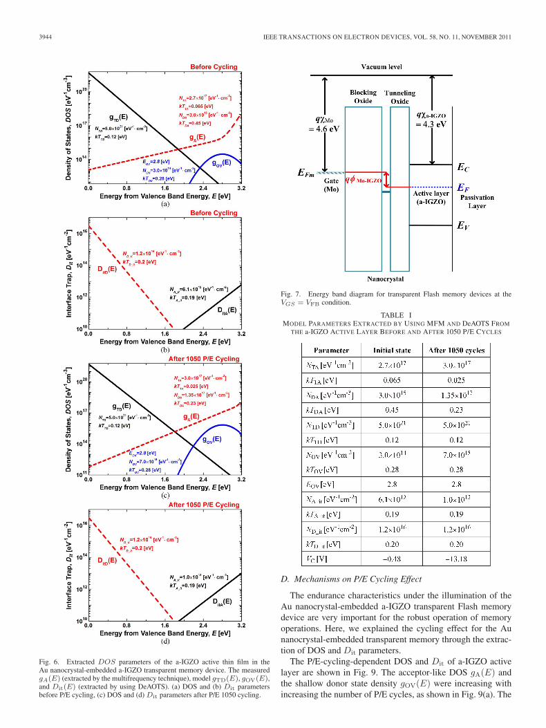
Fig. 5(a) and (b) show the subgap acceptor-like DOS at theinitial state and after 1050 P/E cycles. The subgap acceptor-like DOS was increased with increasing the number of P/Ecycles. In particular, we observed that the deep acceptor-likeDOS gDA(E) was significantly increased after P/E cycles, andthis results in a positive shift of VT with increasing P/E cycles.
The shallow donor state (equivalent to the oxygen vacancystate, i.e., VO → V 2+
O + 2e−) and the interface trap Dit wereextracted by the DeAOTS based on the acceptor-like DOS.Fig. 6 shows the P/E-cycle-dependent DOS and Dit. The donor-like DOS gD(E) [the valence band tail state density gTD(E)and the shallow donor state density gOV(E); in eV−1cm−3] andthe interface-trap density Dit(E) [the acceptor-like interface-trap density DitA(E) and the donor-like interface-trap densityDitD(E); in eV−1cm−2] of the a-IGZO films were presumablymodeled as
gD(E) = gTD(E) + gOV(E)
=NTD × exp(
EV − E
kTTD
)
+ NOV exp
[−
(EOV − E
kTOV
)2]
(2)
Dit(E) =DitA(E) + DitD(E)
=NA_it exp(
E − EC
kTA_it
)
+ ND_it exp(
EV − E
kTD_it
). (3)
Fig. 5. Extracted gA(E) for various combinations of f1, f2, and f3. Theacceptor-like DOS is confirmed to be immune to the range of frequencycombinations in the multifrequency C–V characterization (f1, f2, f3 = 10,100, 500 kHz, respectively).
Therefore, parameters NTD, kTTD, NOV, kTOV, EOV,NA_it, kTA_it, ND_it and kTD_it in gTD(E), gOV(E),DitA(E), and DitD(E) can act as fitting parameters, in contrastwith the gA(E) parameters. On the other hand, the flat-bandvoltage VFB and EFB (defined as the energy difference betweenthe Fermi level EF and the conduction band minimum EC atthe VGS = VFB condition) are calculated below.
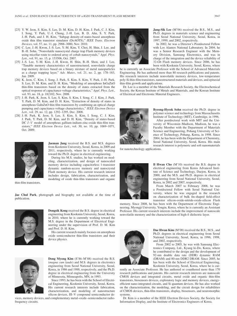
Fig. 7 shows the energy band diagram at the flat-band(VGS = VFB) condition. Assuming that the gate is made ofmolybdenum, for example, VFB is calculated from the workfunction difference φMo − φIGZO and the charge density perunit area in the gate oxide QOX, as described by
VFB = φMO − φIGZO − QOX
COX(4)
φMO − φIGZO = (χMO − χIGZO) − EFB
q(5)
where COX = εOX/TOX and TOX (= Tbot + Ttop) are theoxide capacitance per unit area and the thickness of the gateinsulator, respectively. The extracted physical parameters of thea-IGZO active layer were summarized in Table I.
In Fig. 8, the measured and simulated IDS–VGS curvesbefore cycling and after 1050 P/E cycles are comparativelyshown in linear and log scales for the experimental data plottedwith simulation results from the DeAOTS. The results agreevery well for the initial and P/E-cycled cases.
3944 IEEE TRANSACTIONS ON ELECTRON DEVICES, VOL. 58, NO. 11, NOVEMBER 2011
Fig. 6. Extracted DOS parameters of the a-IGZO active thin film in theAu nanocrystal-embedded a-IGZO transparent memory device. The measuredgA(E) (extracted by the multifrequency technique), model gTD(E), gOV(E),and Dit(E) (extracted by using DeAOTS). (a) DOS and (b) Dit parametersbefore P/E cycling, (c) DOS and (d) Dit parameters after P/E 1050 cycling.
Fig. 7. Energy band diagram for transparent Flash memory devices at theVGS = VFB condition.
TABLE IMODEL PARAMETERS EXTRACTED BY USING MFM AND DeAOTS FROM
THE a-IGZO ACTIVE LAYER BEFORE AND AFTER 1050 P/E CYCLES
D. Mechanisms on P/E Cycling Effect
The endurance characteristics under the illumination of theAu nanocrystal-embedded a-IGZO transparent Flash memorydevice are very important for the robust operation of memoryoperations. Here, we explained the cycling effect for the Aunanocrystal-embedded transparent memory through the extrac-tion of DOS and Dit parameters.
The P/E-cycling-dependent DOS and Dit of a-IGZO activelayer are shown in Fig. 9. The acceptor-like DOS gA(E) andthe shallow donor state density gOV(E) were increasing withincreasing the number of P/E cycles, as shown in Fig. 9(a). The

JANG et al.: ENDURANCE CHARACTERISTICS OF a-IGZO TRANSPARENT FLASH MEMORY 3945
Fig. 8. Measured IDS–VGS curves (red line and symbol) before cycling and(blue line and symbol) after P/E 1050 cycling. (a) IDS–VGS curve in the linearscale. (b) IDS–VGS curve in the log scale compared with the simulation resultsfrom the DeAOTS. They agree very well, depending of the number of P/Ecycles.
increased acceptor-like DOS can be expected to shift VT in apositive direction due to electron trapping in the increased DOS.On the other hand, the increased shallow donor traps result in anegative shift of VT . We also note that the Subthreshold Swing(SSW) is degraded by the increased acceptor-like interface-trapdensity DitA(E) caused by the P/E cycles as shown in Fig. 9(b).
Fig. 10 shows the energy band diagram to explain thephysical mechanism for the endurance characteristics of thea-IGZO transparent memory devices. The negative shift of VC
was experimentally observed with increasing the number ofP/E cycles.
According to the analysis of the extracted DOS and Dit,the VC shift was possible in the both negative and positivedirections. First, the increased acceptor-like DOS may causea positive shift of VC by the electron trapping in the a-IGZOchannel layer. Second, the increased shallow donor traps withthe increased ionization of oxygen vacancies (VO → V 2+
O +2e−) may cause a negative shift of VC by the electron de-trapping in the a-IGZO channel through the conduction bandminimum and the carrier generation. Third, a hole injection intothe gate insulator during the erase operation under illuminationcondition with accelerated electric field by energy band bendinginduced due to generated holes may cause a negative shift ofVC by the injected hole charge QOX in the gate insulator. Weobserved the final shift of the center voltage ∆VC = −12.7 V.
Fig. 9. P/E-cycling-dependent DOS and Dit of the a-IGZO active layer.(a) gA(E) and gOV(E), and (b) DitA(E) increased with increasing thenumber of P/E cycling.
Fig. 10. Energy band diagram illustrating the mechanisms of Au nanocrystal-embedded a-IGZO transparent memory devices after P/E cycling.
With the SSW degradation caused by the increased interfacetraps, the interface-trap states was increased with the increasingnumber of program cycles (SSW : 1.2 → 1.85 V/dec).
A shift in VC with P/E cycles can be explained by threemain mechanisms supported by the quantitative extraction bythe DeAOTS, as shown in Fig. 11. The increased acceptor-like DOS causes ∆VC = ∆VAcceptor−like DOS = 1.4 V and theinjected holes in the gate insulator during the erase operationcause ∆VC = ∆VOX = −10.4 V, and the increased shallowdonor state causes ∆VC = ∆VOV = −3.7 V. Finally, the netshift of the center voltage ∆VC = −12.7 V was resulted andagrees with the experimental observation. ∆VOX in Fig. 11

3946 IEEE TRANSACTIONS ON ELECTRON DEVICES, VOL. 58, NO. 11, NOVEMBER 2011
Fig. 11. Quantitative analysis of the P/E-cycle-induced VT shift.
comes from the ∆QOX in (4). Among ∆VAcceptor−like DOS,∆VOX and ∆VOV, the net ∆VC is dominated by ∆VOX asshown in Fig. 11. Therefore, the main mechanism on the P/Ecycling-induced change in VC was found to be the acceleratedinjection of holes into the gate insulator due to the energy bandbending during the erase operation.
IV. CONCLUSION
In this paper, Au nanocrystal-embedded a-IGZO transparentFlash memory devices have been fabricated and characterizedwith Au nanocrystals as a charge storage layer and a-IGZOfilms as an active layer. The transparent memory device per-formance and operation mechanisms were investigated. Theendurance characteristics and the related physical mechanismsof the Au nanocrystal-embedded a-IGZO transparent memorydevice have been explained through the extracted physicalparameters of the a-IGZO active layer including DOS andDit by the MFM technique and the DeAOTS simulator. Thememory window has been remained the same after 1050 P/Ecycles; however VC has been shifted in a negative direction withincreasing the P/E cycles. Typically, the effect has been reportedand explained to be similar to the negative-bias illuminationstress effect. Thus, the P/E cycle-dependent negative VC shifthas been explained by the extracted DOS and Dit changes withincreasing P/E cycles. Through a simulation, it was found thatthe main mechanism of a shift in VC is due to the acceleratedhole injection into the gate insulator during the erase conditioncaused by the energy band bending.
Through this paper, we have observed that we need morestudies for the improved performance and the robust reliabilityof transparent Flash memory devices for practical implementa-tion for integrated display systems with embedded nonvolatilememory devices. In addition, the physical-parameter-basedanalysis method for the reliability of the transparent memorydevice is expected to be helpful for the next-generation trans-parent memory devices.
REFERENCES
[1] S. Ju, A. Facchetti, Y. Xuan, J. Liu, F. Ishikawa, P. Ye, C. Zhou,T. J. Marks, and D. B. Janes, “Fabrication of fully transparent nanowiretransistors for transparent and flexible electronics,” Nat. Nanotechnol.,vol. 2, pp. 378–384, Jun. 2007.
[2] J. F. Wager, “Transparent electronics,” Science, vol. 300, no. 5623,pp. 1245–1246, May 2003.
[3] S. Masuda, K. Kitamura, Y. Okumura, S. Miyatake, H. Tabata, andT. Kawai, “Transparent thin film transistors using ZnO as an active chan-nel layer and their electrical properties,” J. Appl. Phys., vol. 93, no. 3,pp. 1624–1630, Feb. 2003.
[4] R. L. Hoffman, B. J. Norris, and J. F. Wager, “ZnO-based transparentthin-film transistors,” Appl. Phys. Lett., vol. 82, no. 5, pp. 733–735,Feb. 2003.
[5] K. Nomura, H. Ohta, K. Ueda, T. Kamiya, M. Hirano, and H. Hosono,“Thin-film transistor fabricated in single-crystal transparent oxide semi-conductor,” Science, vol. 300, no. 5623, pp. 1269–1272, May 2003.
[6] K. Nomura, H. Ohta, A. Takagi, T. Kamiya, M. Hirano, and H. Hosono,“Room-temperaure fabrication of transparent flexible thin-film transistorsusing amorphous oxide semiconductors,” Nature, vol. 432, no. 7016,pp. 488–492, Nov. 2004.
[7] J. Y. Kwon, K. S. Son, J. S. Jung, T. S. Kim, M. K. Ryu, K. B. Park,B. W. Yoo, J. W. Kim, Y. G. Lee, K. C. Park, S. Y. Lee, and J. M. Kim,“Bottom-gate gallium indium zinc oxide thin-film transistor array forhigh-resolution AMOLED display,” IEEE Electron Device Lett., vol. 29,no. 12, pp. 1309–1311, Dec. 2008.
[8] Y. Ohta, Y. Chikama, T. Hara, Y. Mizuno, T. Aita, M. Takei, M. Suzuki,O. Nakagawa, Y. Harumoto, H. Nishiki, and N. Kimura, “Amorphous In-Ga-Zn-O TFT-LCDs with high reliability,” in Proc. Int. Display Work-shop, Dec. 2009, pp. 1685–1688.
[9] J. Sakata, H. Ohara, M. Sasaki, T. Osada, H. Miyake, H. Shishido,J. Koyama, Y. Oikawa, H. Maruyama, M. Sakakura, T. Serikawa, and S.Yamazaki, “Development of 4.0-in. AMOLED display with driver circuitusing amorphous In-Ga-Zn-Oxide TFTs,” in Proc. Int. Display Workshop,Dec. 2009, pp. 689–692.
[10] J.-H. Lee, D.-H. Kim, D.-J. Yang, S.-Y. Hong, K.-S. Yoon, P.-S. Hong,C.-O. Jeong, H.-S. Park, S. Y. Kim, S. K. Lim, and S. S. Kim, “World’slargest (15-inch) XGA AMLCD panel using IGZO oxide TFT,” SID Dig.Tech. Papers, vol. 39, no. 1, pp. 625–628, May 2008.
[11] T. Kamiya, K. Nomura, and H. Hosono, “Present status of amorphousI–In-Ga-Zn-O thin-filmtransistors,” Sci. Technol. Adv. Mater., vol. 11,pp. 044305-1–044305-23, Sep. 2010.
[12] J. K. Jeong, “The status and perspectives of metal oxide thin-film transis-tors for active matrixflexible displays,” Semicond. Sci. Technol., vol. 26,pp. 034008-1–034008-10, Feb. 2011.
[13] Z. Liu, C. Lee, V. Narayanan, G. Pei, and E. C. Kan, “Metal nanocrystalmemories-Part I: Device design and fabrication,” IEEE Trans. ElectronDevices, vol. 49, no. 9, pp. 1606–1613, Sep. 2002.
[14] T.-H. Hou, C. Lee, V. Narayanan, U. Ganguly, and E. C. Kan, “Designoptimization of metal nanocrystal memory—Part I: Nanocrystal arrayengineering,” IEEE Trans. Electron Devices, vol. 53, no. 12, pp. 3095–3102, Dec. 2006.
[15] J. Jang, C. Choi, J.-S. Lee, K.-S. Min, J. Lee, D. M. Kim, andD. H. Kim, “Design of gate stacks for improved program/erase speed,retention and process margin aiming next generation metal nanocrystalmemories,” Semicond. Sci. Technol., vol. 24, pp. 115009-1–115009-11,Oct. 2009.
[16] J. W. Seo, J.-W. Park, K. S. Lim, J.-H. Yang, and S. J. Kang, “Transparentresistive random access memory and its characteristics for nonvolatileresistive switching,” Appl. Phys. Lett., vol. 93, p. 223505, Dec. 2008.
[17] C. H. Park, S. Im, J. Yun, G. H. Lee, B. H. Lee, and M. M. Sung, “Trans-parent photostable ZnO nonvolatile memory transistor with ferroelectricpolymer and sputter-deposited oxide gate,” Appl. Phys. Lett., vol. 95,p. 223506, Dec. 2009.
[18] H. Yin, S. Kim, H. Lim, Y. Min, C. J. Kim, I. Song, J. Park, S.-W. Kim,A. Tikhonovsky, J. Hyun, and Y. Park, “Program/Erase Characteristicsof Amorphous Gallium Indium Zinc Oxide Nonvolatile Memory,” IEEETrans. Electron Devices, vol. 55, no. 8, pp. 2071–2077, Aug. 2008.
[19] H. Yin, S. Kim, C. J. Kim, I. Song, J. Park, S. Kim, and Y. Park, “Fullytransparent nonvolatile memory employing amorphous oxides as chargetrap and transistor’s channel layer,” Appl. Phys. Lett., vol. 93, p. 172109,Oct. 2008.
[20] A. Suresh, S. Novak, P. Wellenius, V. Misra, and J. F. Muth, “Transparentindium gallium zinc oxide transistor based floating gate memory withplatinum nanoparticles in the gate dielectric,” Appl. Phys. Lett., vol. 94,p. 123501, Mar. 2009.
[21] Y.-S. Park, S. Y. Lee, and J.-S. Lee, “Nanofloating gate memory devicesbased on controlled metallic nanoparticle-embedded InGaZnO TFTs,”IEEE Electron Device Lett., vol. 31, no. 10, pp. 1134–1136, Oct. 2010.
[22] S. Lee, S. Park, S. Kim, Y. Jeon, K. Jeon, J.-H. Park, J. Park, I. Song,C. J. Kim, Y. Park, D. M. Kim, and D. H. Kim, “Extraction of sub-gap density of states in amorphous InGaZnO thin-film transistors byusing multifrequency capacitance-voltage characteristics,” IEEE ElectronDevice Lett., vol. 31, no. 3, pp. 231–233, Mar. 2010.
JANG et al.: ENDURANCE CHARACTERISTICS OF a-IGZO TRANSPARENT FLASH MEMORY 3947
[23] Y. W. Jeon, S. Kim, S. Lee, D. M. Kim, D. H. Kim, J. Park, C. J. Kim,I. Song, Y. Park, U.-I. Chung, J.-H. Lee, B. D. Ahn, S. Y. Park,J.-H. Park, and J. H. Kim, “Subgap density-of-states-based amorphousoxide thin film transistor simulator (DeAOTS),” IEEE Trans. ElectronDevices, vol. 57, no. 11, pp. 2988–3000, Nov. 2010.
[24] C. Lee, J.-H. Kwon, J.-S. Lee, Y.-M. Kim, Y. Choi, H. Shin, J. Lee, andB.-H. Sohn, “Nonvolatile nanocrystal charge trap Flash memory devicesusing micellar route to ordered array of cobalt nanocrystals,” Appl. Phys.Lett., vol. 91, no. 15, p. 153506, Oct. 2007.
[25] J.-S. Lee, Y.-M. Kim, J.-H. Kwon, H. Shin, B.-H. Shon, and J. Lee,“Tunable memory characteristics of nanostructured, nonvolatile chargetrap memory devices based on a binary mixture of metal nanoparticlesas a charge trapping layer,” Adv. Mater., vol. 21, no. 2, pp. 178–183,Jan. 2009.
[26] K. Jeon, C. Kim, I. Song, J. Park, S. Kim, S. Kim, Y. Park, J.-H. Park,S. Lee, D. M. Kim, and D. H. Kim, “Modeling of amorphous InGaZnOthin-film transistors based on the density of states extracted from theoptical response of capacitance-voltage characteristics,” Appl. Phys. Lett.,vol. 93, no. 18, p. 182102, Nov. 2008.
[27] J.-H. Park, K. Jeon, S. Lee, S. Kim, S. Kim, I. Song, C. J. Kim, J. Park,Y. Park, D. M. Kim, and D. H. Kim, “Extraction of density of states inamorphous GaInZnO thin film transistors by combining an optical chargepumping and capacitance-voltage characteristics,” IEEE Electron DeviceLett., vol. 29, no. 12, pp. 1292–1295, Dec. 2008.
[28] J.-H. Park, K. Jeon, S. Lee, S. Kim, S. Kim, I. Song, C. J. Kim,J. Park, Y. Park, D. M. Kim, and D. H. Kim, “Density of states-basedDC I–V model of amorphous gallium-indium-zinc-oxide thin-film tran-sistors,” IEEE Electron Device Lett., vol. 30, no. 10, pp. 1069–1071,Oct. 2009.
Jaeman Jang received the B.S. and M.S. degreesfrom Kookmin University, Seoul, Korea, in 2009 and2011, respectively, where he is currently workingtoward the Ph.D. degree in electrical engineering.
During his M.S. studies, he has worked on mod-eling, characterization, and design of nanoscaledmemory device including capacitorless 1-transistordynamic random-access memory and nanocrystalFlash memory device. His current research interestincludes design, fabrication, characterization, andmodeling of oxide thin-film transistors and organic
thin-film transistors.
Jae Chul Park, photograph and biography not available at the time ofpublication.
Dongsik Kong received the B.S. degree in electricalengineering from Kookmin University, Seoul, Korea,in 2010, where he is currently working toward theM.S. degree in the Department of Electrical Engi-neering under the supervision of Prof. D. M. Kimand Prof. D. H. Kim.
His current research mainly focuses on amorphousoxide semiconductor thin-film transistors and theirdevice physics.
Dong Myong Kim (S’86–M’88) received the B.S.(magna cum laude) and M.S. degrees in electronicsengineering from Seoul National University, Seoul,Korea, in 1986 and 1988, respectively, and the Ph.D.degree in electrical engineering from the Universityof Minnesota, Minneapolis, MN, in 1993.
Since 1993, he has been with the School of Electri-cal Engineering, Kookmin University, Seoul, Korea.His current research interests include fabrication,characterization, and modeling of nanostructuresilicon devices, III–V compound semiconductor de-
vices, memory devices, and complementary metal–oxide–semiconductor radio-frequency circuits.
Jang-Sik Lee (M’06) received the B.S., M.S., andPh.D. degrees in materials science and engineeringfrom Seoul National University, Seoul, Korea, in1997, 1999, and 2002, respectively.
In 2002, he was a Director’s Postdoctoral Fellowwith Los Alamos National Laboratory. In 2004, hewas a Senior Research Engineer with the Mem-ory Division, Samsung Electronics, and was incharge of the integration and the device reliability of32-Gb Flash memory devices. Since 2006, he hasbeen with Kookmin University, Seoul, Korea, where
he is currently an Associate Professor with the School of Advanced MaterialsEngineering. He has authored more than 80 research publications and patents.His research interests include nonvolatile memory devices, low-temperaturepoly-Si thin-film transistors, nanostructured materials and devices, and epitaxialthin-film growth and applications.
Dr. Lee is a member of the Materials Research Society, the ElectrochemicalSociety, the Korean Institute of Metals and Materials, and the Korean Instituteof Electrical and Electronic Material Engineers.
Byeong-Hyeok Sohn received the Ph.D. degree inpolymer science and technology from MassachusettsInstitute of Technology (MIT), Cambridge, in 1996.
After postdoctoral work with MIT and the Uni-versity of Wisconsin–Madison, Madison, he was aFaculty Member with the Department of MaterialsScience and Engineering, Pohang University of Sci-ence of Technology, Pohang, Korea, in 1998. Since2004, he has been with the Department of Chemistry,Seoul National University, Seoul, Korea. His mainresearch interest is polymeric and soft nanomaterials
for nanotechnology applications.
Il Hwan Cho (M’10) received the B.S. degree inelectrical engineering from Korea Advanced Insti-tute of Science and Technology, Daejon, Korea, in2000, and the M.S. and Ph.D. degrees in electricalengineering from Seoul National University, Seoul,Korea, in 2002 and 2007, respectively.
From March 2007 to February 2008, he wasa Postdoctoral Fellow with Seoul National Uni-versity, where he was engaged in the researchon characterization of bulk fin-shaped field-effecttransistor silicon-oxide-nitride-oxide-silicon Flash
memory. Since 2008, he has been with the Department of Electronic Engi-neering, Myongji University, Yongin, Korea, where he is currently an AssistantProfessor. His current research interests include the improvement of nanoscalenonvolatile memory and the characterization of high-k dielectric layer.
Dae Hwan Kim (M’08) received the B.S., M.S., andPh.D. degrees in electrical engineering from SeoulNational University, Seoul, Korea, in 1996, 1998,and 2002, respectively.
From 2002 to 2005, he was with Samsung Elec-tronics Company, Ltd., Kyung ki-Do, Korea, wherehe contributed to the design and the development of92-nm double data rate (DDR) dynamic RAM(DRAM) and 80-nm DDR2 DRAM. Since 2005, hehas been with the School of Electrical Engineering,Kookmin University, Seoul, Korea, where he is cur-
rently an Associate Professor. He has authored or coauthored more than 170research publications and patents. His current research interests are nanoscaleCMOS devices and integrated circuits, metal oxide and organic thin-filmtransistors, biosensors devices, exploratory logic and memory devices, energy-efficient nano-integrated circuits, and Si quantum devices. He has also workedon the characterization, the modeling, and the circuit design for reliabilitiesof CMOS devices, thin-film transistors, display, biosensors, and neuromorphicsystems.
Dr. Kim is a member of the IEEE Electron Devices Society, the Society forInformation Display, and the Institute of Electronics Engineers of Korea.