Embed Size (px)
Citation preview

Renata Oliveira de Sousa
Energy Storage Requirements and Wear-out
of MMCC based STATCOM: The Role of the
Modulation Strategy
Belo Horizonte, MG
2019


Renata Oliveira de Sousa
Energy Storage Requirements and Wear-out of MMCC
based STATCOM: The Role of the Modulation Strategy
Dissertacao submetida a banca examinadora
designada pelo Colegiado do Programa de
Pos-Graduacao em Engenharia Eletrica do
Centro Federal de Educacao Tecnologica de
Minas Gerais e da Universidade Federal de
Sao Joao Del Rei, como parte dos requisitos
necessarios a obtencao do grau de Mestre em
Engenharia Eletrica.
Centro Federal de Educacao Tecnologica de Minas Gerais
Programa de Pos-Graduacao em Engenharia Eletrica
Orientador: Prof. Dr. Heverton Augusto Pereira
Belo Horizonte, MG
2019

Elaboração da ficha catalográfica pela Biblioteca-Campus II / CEFET-MG
Sousa, Renata, Oliveira de.
S729e Energy storage requirements an Wear-out of MMCC based
STATCOM: the role of the modulation strategy / Renata Oliveira de
Sousa. – 2019.
87 f.: il., gráfs, tabs.
Dissertação de mestrado apresentada ao Programa de Pós-Graduação
em Engenharia Elétrica em associação ampla entre a UFSJ e o CEFET-
MG.
Orientador: Heverton Augusto Pereira.
Dissertação (mestrado) – Centro Federal de Educação Tecnológica de
Minas Gerais.
1. Sincronização – Teses. 2. Programação modular – Teses.
3. Conversores de correntes elétricas – Teses. 4. Teoria da modulação –
Teses. 5. Desgaste mecânico – Teses. 6. Energia – Armazenamento –
Teses. I. Pereira, Heverton Augusto. II. Centro Federal de Educação
Tecnológica de Minas Gerais. III. Universidade Federal de São João del-
Rei. IV. Título.
CDD 621.31912

A minha famılia, mentores e amigos.


Agradecimentos
Primeiramente, agradeco aos meus pais, Sebastiao e Gloria, por todo apoio incon-
dicional. Obrigada por me ensinarem a ir atras dos meus sonhos por mais que os caminhos
sejam dificeis. Aos demais familiares e a todos os amigos que contribuıram para essa
conquista. Aos professores que me orientaram neste trabalho, Prof. Allan Cupertino e
Prof. Heverton Pereira. Aos membros do grupo de pesquisa GESEP, em especial aos mem-
bros Joao Victor, Dayane, William e Rodrigo, por todo companherismo e conhecimento
compartilhado. Por fim, agradeco ao CEFET-MG pelo apoio financeiro.


“Dark times lie ahead of us and there will be a time when
we must choose between what is easy and what is right.”
(J. K. Rowling)


Resumo
Os sistemas de distribuicao e transmissao possuem uma enorme variedade de cargas. No
entanto, a maioria dessas cargas e nao-resistiva ou flutuante. Essas cargas podem gerar
variacoes de tensao que afetam a operacao e a eficiencia dos sistemas. Para minimizar esses
problemas, a compensacao de potencia reativa e indicada. Neste contexto, o Compensador
Sıncrono Estatico (STATCOM, do ingles Static Synchronous Compensator) tem sido
amplamente utilizado. O principal desafio no projeto de STATCOMs de media e alta
tensao e definir uma topologia de conversor que deve atingir nıveis altos de potencia e tensao
com chaves semicondutoras padrao. Neste contexto, a topologia Double-Star Chopper Cell
(DSCC), da famılia de Conversores Modulares Multinıveis em Cascata, provou ser uma
opcao atraente para aplicacoes STATCOM de media e alta tensao. No entanto, a topologia
DSCC apresenta alguns desafios relacionados a estrategias de modulacao, requisitos de
armazenamento de energia e confiabilidade. Em relacao ao requisito de armazenamento
de energia, a literatura considera no projeto as tensoes dos capacitores balanceadas. No
entanto, dependendo da estrategia de modulacao, as tensoes do capacitor oscilam dentro de
um intervalo e com um espalhamento. Em termos de confiabilidade, a literatura apresenta
trabalhos nos quais e avaliado o tempo de vida util do DSCC. Entretanto, nenhum desses
trabalhos leva em conta o efeito nao desprezıvel do ripple de tensao nos capacitores da
celula e tambem como a estrategia de modulacao pode afetar esse ripple de tensao e,
consequentemente, a vida util do capacitor. Portanto, este trabalho considera o efeito
de todos os componentes da celula (ou seja, dispositivos semicondutores e capacitores) e
analisa o impacto das estrategias de modulacao na vida util de um DSCC-STATCOM.
Para este proposito, duas estrategias de modulacao sao selecionadas: PS-PWM (do ingles
Phase-Shifted Pulse-Width Modulation) e NLC-CTB (do ingles Nearest-Level Control with
Cell Tolerance Band algorithm). Alem disso, este trabalho apresenta o ındice de fator de
espalhamento para comparar diferentes estrategias de modulacao em termos de capacidade
de balanceamento de tensao do capacitor. Alem disso, os requisitos de armazenamento
de energia para cada estrategia de modulacao sao discutidos. Para analisar o efeito do
ripple da tensao do capacitor da celula na vida util, a metodologia que melhor representa
seu efeito no modelo de vida util do capacitor, bem como sua frequencia de amostragem,
sao investigadas. Os resultados indicaram que diferentes estrategias de modulacao podem
exigir armazenamento de energia distintos. De fato, o NLC-CTB requer armazenamento
de energia 44 % maior que o PS-PWM. Como consequencia, o numero de capacitores afeta
o tempo de vida util do banco de capacitores. Por outro lado, as estrategias de modulacao
podem produzir diferentes perdas de energia que tambem afetam o tempo de vida util das
chaves e geram custos adicionais.

Palavras-chaves: STATCOM; Conversor Modular Multinıvel em Cascata; Estrategia de
Modulacao; Analise de desgaste; Requisito de armazenamento de energia.

Abstract
The distribution and transmission systems supply a huge variety of loads. Nevertheless,
most of these loads are non-resistive or fluctuating. These loads can generate voltage
variations which affect the operation and efficiency of the systems. In order to minimize
these problems, reactive power compensation is indicated. In this context, the Static
Synchronous Compensator (STATCOM) has been widely used. The major challenge in the
design of medium and high voltage STATCOMs is to define a converter topology which
must reach higher power and voltage levels with standard rated semiconductor switches.
In this context, the topology Double-Star Chopper Cell (DSCC), member of the Modular
Multilevel Cascade Converter family, has proved to be an attractive option for medium and
high voltage STATCOM applications. Nevertheless, the DSCC topology has some challenges
in the modulation schemes, energy storage requirements and reliability. Regarding the
energy storage requirement the literature considers balanced capacitor voltages in the design.
However, depending on the modulation strategy, the capacitor voltages oscillate within a
range and with a spreading. In terms of reliability, the literature presents works in which is
evaluated the DSCC lifetime. Nevertheless, none of these works take into account the effect
of the non-negligible voltage ripple in the cell capacitors and also how the modulation
strategy can affect this capacitor voltage ripple and, consequently, the capacitor lifetime.
Therefore, this work considers the effect of all cell components (i.e. semiconductor devices
and capacitors) and analyzes the modulation strategies impact on the energy storage
requirements and reliability of a DSCC-STATCOM. For this purpose, two modulation
strategies are selected: Phase-Shifted Pulse-Width Modulation (PS-PWM) and Nearest-
Level Control with Cell Tolerance Band algorithm (NLC-CTB). In addition, this work
introduces the spreading factor index to compare different modulation strategies in terms
of capacitor voltage balancing capability. Additionally, the energy storage requirements
for each modulation strategy are discussed. In order to analyze the cell capacitor voltage
ripple effect on lifetime, the methodology which better represent its effect on the capacitor
lifetime model as well as its sampling frequency are investigated. Moreover, the results
indicated that different modulation strategies may require distinct energy storage. In
fact, the NLC-CTB requires energy storage 44 % higher than PS-PWM. As consequence,
different capacitor numbers impact on the lifetime of the capacitor bank. On the other
hand, the modulation strategies may produce different power losses which also impact on
the lifetime and produce additional costs.
Key-words: STATCOM; Modular Multilevel Cascade Converter; Modulation Strategy;
Wear-out Analysis; Energy Storage Requirement.


List of Figures
Figure 1 – Reactive power compensators: (a) Fixed Series Capacitors; (b) Thyristor-
controlled Series Capacitor (c) Fixed Shunt Capacitor/Inductor Bank;(d)
Static Var Compensator; (e) Synchronous Condenser; (f) Static Syn-
chronous Compensator. . . . . . . . . . . . . . . . . . . . . . . . . . . . 28
Figure 2 – STATCOM technologies: (a) Two-level converter; (b) Two-level con-
verter with series-connected switches; (c)Three-level NPC; (d) FCC; (e)
CHB; (f) MMC. . . . . . . . . . . . . . . . . . . . . . . . . . . . . . . . 30
Figure 3 – MMCC configuration. (a) SDBC; (b) SSBC; (c) DSCC or DSBC; (d)
Bridge Cell; (e) Chopper Cell. . . . . . . . . . . . . . . . . . . . . . . . 32
Figure 4 – Schematic of the DSCC-STATCOM. . . . . . . . . . . . . . . . . . . . 37
Figure 5 – Control strategy for DSCC-STATCOM: (a) grid current control; (b)
circulating current control; (c) individual voltage balancing control. . . 38
Figure 6 – Schematic of PS-PWM strategy. . . . . . . . . . . . . . . . . . . . . . . 41
Figure 7 – Comparison of (N + 1) and (2N + 1) level phase-shifted modulation
schemes: (a) DSCC output voltage; (b) DSCC internal voltage. Operating
Conditions: 4 cells per arm, switching frequency of 900 Hz. . . . . . . . 42
Figure 8 – Schematic of NLC-CTB strategy. . . . . . . . . . . . . . . . . . . . . . 43
Figure 9 – Flowchart of CTB algorithm (Adapted from Sharifabadi et al. (2016)). 43
Figure 10 – Operation of PS-PWM (SOUSA et al., 2018). . . . . . . . . . . . . . . 45
Figure 11 – Operation of NLC-CTB (SOUSA et al., 2018). . . . . . . . . . . . . . . 46
Figure 12 – Reactive power profile. . . . . . . . . . . . . . . . . . . . . . . . . . . . 49
Figure 13 – Reactive power response. . . . . . . . . . . . . . . . . . . . . . . . . . . 50
Figure 14 – Grid current: (a) NLC-CTB dynamic; (b) detail in rated inductive
operation employing NLC-CTB; (c) detail in rated capacitive opera-
tion employing NLC-CTB; (d)PS-PWM dynamic; (e) detail in rated
inductive operation employing PS-PWM; (f) detail in rated capacitive
operation employing PS-PWM. . . . . . . . . . . . . . . . . . . . . . . 50
Figure 15 – Detail of the spectrum of the grid current (calculated by Fast Fourier
Transform) in rated capacitive operation: (a) NLC-CTB ; (b) PS-PWM. 51
Figure 16 – Circulating current of phase A. . . . . . . . . . . . . . . . . . . . . . . 51
Figure 17 – (a) Capacitor voltage dynamics on the upper arm of phase A; (b) detail
in inductive operation; (c) detail in capacitive operation. . . . . . . . . 51
Figure 18 – Upper arm capacitor voltages for different switching frequencies: (a) 210
Hz; (b) 570 Hz. Operating Conditions: DSCC Parameters of Tab. 3, rated
capacitive reactive power, 40 kJ/MVA of energy storage requirement and
modulation strategy PS-PWM. . . . . . . . . . . . . . . . . . . . . . . . 53

Figure 19 – Correlation between individual cell voltage and arm cell average voltage.
Operating Conditions: DSCC Parameters of Tab. 3, rated capacitive
reactive power, 40 kJ/MVA of energy storage requirement and modulation
strategy PS-PWM. . . . . . . . . . . . . . . . . . . . . . . . . . . . . . 54
Figure 20 – Comparison of capacitor balancing performance of the studied modula-
tion strategies: (a) Spreading factor, considering Wconv = 40 kJ/MVA;
(b) Energy storage requirements. . . . . . . . . . . . . . . . . . . . . . 55
Figure 21 – (a) Capacitor voltage dynamics on the upper arm of phase A; (b) detail
in inductive operation; (c) detail in capacitive operation. . . . . . . . . 56
Figure 22 – Capacitor voltages for: (a) NLC-CTB without capacitance tolerance;
(b) NLC-CTB with 10 % capacitance tolerance; (c) PS-PWM without
capacitance tolerance; (d) PS-PWM with 10 % capacitance tolerance. . 57
Figure 23 – Bathtub failure curve divided into three periods. . . . . . . . . . . . . . 61
Figure 24 – Schematic of an IGBT module (Adapted from ABB (2014)). . . . . . . 62
Figure 25 – Lifetime evaluation flowchart of semiconductor devices. . . . . . . . . . 63
Figure 26 – Hybrid thermal model based on Foster and Cauer models. . . . . . . . 64
Figure 27 – Lifetime evaluation flowchart of the capacitor. . . . . . . . . . . . . . . 67
Figure 28 – (a) Capacitor voltage considering the voltages of cell reference, arm
average and individual cell; (b) Capacitor voltage sampling. Operating
Conditions: Parameters of Tab. 3, case study PS-5C and rated capacitive
operation. . . . . . . . . . . . . . . . . . . . . . . . . . . . . . . . . . . 69
Figure 29 – Individual capacitor lifetime considering the capacitor voltage as rated
capacitive, inductive and the cell reference for different capacitor voltage
sampling frequencies. Operating Conditions: Parameters of Tab. 3 and
11, Th fixed at 60C, case study PS-5C. Lifetime values normalized by
the lifetime computed considering the cell reference voltage. . . . . . . . 69
Figure 30 – Monte Carlo analysis flowchart. . . . . . . . . . . . . . . . . . . . . . . 70
Figure 31 – Unreliability block diagram of: (a) cell-level; (b) system level. . . . . . 71
Figure 32 – Mission profiles: (a) Reactive Power (Sb = 15 MVA); (b) Ambient
Temperature. . . . . . . . . . . . . . . . . . . . . . . . . . . . . . . . . 73
Figure 33 – For different operation conditions: (a) Conduction and switching losses
(Sb = 15 MVA); (b) Effective switching frequency. . . . . . . . . . . . . 73
Figure 34 – DSCC-STATCOM annual energy losses. . . . . . . . . . . . . . . . . . 74
Figure 35 – (a) Annual profile of hotspot temperature; (b) detail of one week hotspot
temperature; (c) annual profile of case temperature of D2; (d) detail of
one week case temperature. . . . . . . . . . . . . . . . . . . . . . . . . 75
Figure 36 – Life consumption in the cell components (semi-logarithmic scale). . . . 76

Figure 37 – Unreliability function of semiconductor devices DSCC-level (SD), capac-
itors DSCC-level (C) and DSCC system-level (DSCC) for: (a) PS-5C;
(b) PS-7C; (c) NLC-7C. . . . . . . . . . . . . . . . . . . . . . . . . . . 77


List of Tables
Table 1 – Comparison of reactive compensation devices. . . . . . . . . . . . . . . . 29
Table 2 – Examples of STATCOM Products Marketed. . . . . . . . . . . . . . . . 32
Table 3 – DSCC-STATCOM Parameters. . . . . . . . . . . . . . . . . . . . . . . . 48
Table 4 – Parameters of the controllers. . . . . . . . . . . . . . . . . . . . . . . . . 49
Table 5 – Spreading factor for both modulation strategies with and without capac-
itance tolerance. . . . . . . . . . . . . . . . . . . . . . . . . . . . . . . . 57
Table 6 – Capacitor bank design evaluation. . . . . . . . . . . . . . . . . . . . . . 58
Table 7 – Foster and case to heatsink parameters of the thermal model (ABB, 2013b). 64
Table 8 – Cauer parameters of the thermal model. . . . . . . . . . . . . . . . . . . 64
Table 9 – Parameters of the heatsink and water cooling impedances. . . . . . . . . 65
Table 10 – Parameters of the heatsink and water cooling impedances. . . . . . . . . 65
Table 11 – Parameters of the Capacitor Lifetime Model (ELECTRONICON, 2014). 68
Table 12 – Equivalent static values employed in Monte Carlo simulation. . . . . . . 75
Table 13 – Lifetime Evaluation Results. . . . . . . . . . . . . . . . . . . . . . . . . 76


List of abbreviations and acronyms
AC Alternating Current
CHB Cascaded H-bridge Converter
DC Direct Current
DFR Design for Reliability
DSBC Double-Star Bridge Cell
DSCC Double-Star Chopper Cell
FACTS Flexible AC Transmission Systems
FCC Flying Capacitor Converter
HV High Voltage
HVDC High-Voltage Direct Current
IGBT Insulated Gate Bipolar Transistor
LC Life Consumption
LPF Low-Pass Filter
LT Lifetime
MAF Moving Average Filter
MMC Modular Multilevel Converter
MMCC Modular Multilevel Cascade Converter
NLC-7C Converter modulated with NLC-CTB with 7 capacitors per cell
NLC-CTB Nearest-Level Control with Cell Tolerance Band algorithm
NPC Neutral Point Clamped
PCC Point of Common Coupling
PR Proportional Resonant
PS-5C Converter modulated with PS-PWM with 5 capacitors per cell

PS-7C Converter modulated with PS-PWM with 7 capacitors per cell
PS-PWM Phase-Shifted Pulse Width Modulation
pu Per unit
rms Root Mean Square
SC Synchronous Condenser
SDBC Single-Delta Bridge Cell
SSBC Single-Star Bridge Cell
SVC Static Var Compensator
STATCOM Static Synchronous Compensator
TCSC Thyristor-controlled Series Capacitor
THD Total Harmonic Distortion
VSC Voltage Source Converter

List of symbols
Ah Heatsink surface area
B10 Number of cycles where 10 % of the elements of a population fail
C Cell capacitance
CN Individual capacitance
ch specific heat capacity
Ch−w Heatsink-to-water cooling thermal capacitance
cov Covariance
D1 Bottom diode
D2 Top diode
dh Heatsink thickness
Enom Minimum value of the nominal energy storage per arm
Ecell Energy storage per cell
f1 NLC-CTB important frequency 1
f2 NLC-CTB important frequency 2
fg Grid frequency
fi Frequency from Fast Fourier Transform
fma Moving average filter frequency
fs Sampling frequency
fsw Switching frequency
fus Usage factor
f(x) Probability distribution function
F (x) Component unreliability function
FC(x) Capacitor unreliability function

FC,cell(x) Capacitors cell-level unreliability function
FC,DSCC(x) Capacitors DSCC-level unreliability function
Fcell(x) All components cell-level unreliability function
FD,i(x) Semiconductor device unreliability function
FDSCC(x) DSCC system-level unreliability function
FSD,cell(x) Semiconductor devices cell-level unreliability function
FSD,DSCC(x) Semiconductor devices DSCC-level unreliability function
hc Water flow convection coefficient
Ic,i Harmonic amplitude of the capacitor current
In Grid current peak value
ig Grid current
igαβ Grid current stationary frame
il Lower arm current
iu Upper arm current
iz Circulating current
kb Proportional gain of individual balancing control
Ke Spreading Factor
ki,avg Integral gain of average control
kp,avg Proportional gain of average control
kp,g Proportional gain of grid current control
kr,g Resonant gain of grid current control
kp,z Proportional gain of circulating current control
kr,z Resonant gain of circulating current control
La Arm inductance
LC Life Consumption
Leq Equivalent output inductance

LESL Equivalent Series Inductor of a capacitor
Lf Time-to-failure of a capacitor
L0 Rated lifetime of a capacitor
Lg Grid inductance
li Operating time of a capacitor
L[N ] List of cells
m Modulation amplitude index
M number of capacitors in each cell
mmax Maximum modulation index
N Number of cells per arm
Ncap Number of capacitors in the capacitor bank
Nf Number of cycles to failure
ni Number of cycles
n[u,l] Rounded signal
P Active power
Plosses,C Power losses of a capacitor
Plosses,SD Power losses of a semiconductor device
Q Reactive power
Ra Arm inductor resistance
Req Equivalent output resistance
RESR Equivalent Series Resistor
Rg Grid resistance
Rh−w Heatsink-to-water cooling thermal resistance
Rth Capacitor thermal resistance
Rw−a Water cooling-to-ambient thermal resistance
S1 Bottom IGBT

S2 Top IGBT
Sb Power base for per unit computation
Sn STATCOM nominal power
ST Switch of bypass
tan(δ0) Dielectric dissipation factor
Ta Ambient temperature
Tc Case temperature
Th Hotspot temperature
Th,rated Rated hotspot temperature
Tj Junction temperature
T[j,c]m Junction and case average temperature
ton Heating time
va DSCC output voltage
vavg Cell average voltages
vb Output of voltage individual balancing control
Vc Capacitor voltage
Vc,rated Rated capacitor voltage
vcell Cell voltage
vcell,max Maximum voltage of the cell bank
vdc dc-link voltage
Vdc Minimum dc-link voltage
vg Grid voltage
Vg rms grid voltage
vgαβ Grid voltage stationary frame
vin DSCC internal voltage
vl Reference signal for lower arm
vg Grid voltage
vmax Maximum cell voltage
vmin Minimum cell voltage
Vnom Capacitor rated voltage
vs Equivalent output voltage
vs,αβ Equivalent output voltage stationary frame
Vsvc Semiconductor device voltage class
vu Reference signal for upper arm
vz Internal voltage
Wconv Energy storage requirement
Xa Arm impedance
Xg Grid impedance
Xeq STATCOM output impedance
Zc−h Case-to-heatsink thermal impedance
Zh−w Heatsink-to-water cooling thermal impedance
Zj−c,cauer Junction-to-case Foster thermal impedance
Zj−c,foster Junction-to-case Foster thermal impedance
Zw−a water cooling-to-ambient thermal impedance
α Maximum current rise rate
β Angular displacement between the carrier waveforms in the upper and
lower arms
∆Vg Variation in the grid voltage
∆Tj,c Junction and case variation of temperature
λ Modulation gain
λh Thermal conductivity
ρi Pearson correlation coefficient

ρh Material density of the heatsink
σavg Standard deviation of vavg
σcell,i Standard deviation of vcell,i
θu,n Angular displacements of the upper carrier waveforms
θl,n Angular displacements of the lower carrier waveforms
ωc Circulating current LPF cut-off frequencykb
ωn Angular grid frequency
Superscripts
∗ Reference value
′ Equivalent static value
Subscripts
u Upper arm
l Lower arm

Contents
1 INTRODUCTION . . . . . . . . . . . . . . . . . . . . . . . . . . . . . 27
1.1 Context and Relevance . . . . . . . . . . . . . . . . . . . . . . . . . . 27
1.2 STATCOM Physical Realization . . . . . . . . . . . . . . . . . . . . . 29
1.3 DSCC Reliability . . . . . . . . . . . . . . . . . . . . . . . . . . . . . . 33
1.4 Objectives . . . . . . . . . . . . . . . . . . . . . . . . . . . . . . . . . 34
1.5 Contributions . . . . . . . . . . . . . . . . . . . . . . . . . . . . . . . . 34
1.6 Master Thesis Outline . . . . . . . . . . . . . . . . . . . . . . . . . . . 34
1.7 List of Publications . . . . . . . . . . . . . . . . . . . . . . . . . . . . 35
1.7.1 Published Journal Papers . . . . . . . . . . . . . . . . . . . . . . . . . 35
1.7.2 Submitted Journal Papers (under review) . . . . . . . . . . . . . . . . . 35
1.7.3 Published Conference Papers: In cooperation with the research group 35
1.7.4 Submitted Journal Papers (under review): In cooperation with the
research group . . . . . . . . . . . . . . . . . . . . . . . . . . . . . . . 35
2 MODELING, CONTROL AND DESIGN . . . . . . . . . . . . . . . . . 37
2.1 Topology . . . . . . . . . . . . . . . . . . . . . . . . . . . . . . . . . . 37
2.2 Control Strategy . . . . . . . . . . . . . . . . . . . . . . . . . . . . . . 37
2.3 Modulation Strategies . . . . . . . . . . . . . . . . . . . . . . . . . . 40
2.3.1 PS-PWM . . . . . . . . . . . . . . . . . . . . . . . . . . . . . . . . . . . 40
2.3.2 NLC-CTB . . . . . . . . . . . . . . . . . . . . . . . . . . . . . . . . . . 42
2.3.3 Switching and Sampling Frequencies . . . . . . . . . . . . . . . . . . . 44
2.4 Design . . . . . . . . . . . . . . . . . . . . . . . . . . . . . . . . . . . . 46
2.5 Dynamic Response . . . . . . . . . . . . . . . . . . . . . . . . . . . . 48
2.6 Chapter Conclusions . . . . . . . . . . . . . . . . . . . . . . . . . . . 52
3 ENERGY STORAGE REQUIREMENTS . . . . . . . . . . . . . . . . 53
3.1 Spreading Factor . . . . . . . . . . . . . . . . . . . . . . . . . . . . . 53
3.2 Modulation Strategy and Spreading Factor . . . . . . . . . . . . . . 54
3.3 Commercial Design . . . . . . . . . . . . . . . . . . . . . . . . . . . . 57
3.4 Chapter Conclusions . . . . . . . . . . . . . . . . . . . . . . . . . . . 59
4 RELIABILITY OF A DSCC-STATCOM . . . . . . . . . . . . . . . . . 61
4.1 Introduction . . . . . . . . . . . . . . . . . . . . . . . . . . . . . . . . 61
4.2 Lifetime Evaluation . . . . . . . . . . . . . . . . . . . . . . . . . . . . 62
4.2.1 Semiconductor Devices . . . . . . . . . . . . . . . . . . . . . . . . . . 62
4.2.2 Cell Capacitor . . . . . . . . . . . . . . . . . . . . . . . . . . . . . . . . 66

4.2.3 Monte Carlo Based Reliability Evaluation . . . . . . . . . . . . . . . . . 70
4.3 Modulation Strategy Impact on Lifetime . . . . . . . . . . . . . . . . 72
4.4 Chapter Conclusions . . . . . . . . . . . . . . . . . . . . . . . . . . . 77
5 CLOSURE . . . . . . . . . . . . . . . . . . . . . . . . . . . . . . . . . 79
5.1 Conclusions . . . . . . . . . . . . . . . . . . . . . . . . . . . . . . . . 79
5.2 Future Works . . . . . . . . . . . . . . . . . . . . . . . . . . . . . . . . 80
REFERENCES . . . . . . . . . . . . . . . . . . . . . . . . . . . . . . 81
27
1 Introduction
1.1 Context and Relevance
The distribution and transmission systems are complex structures. Nowadays, these
systems supply a huge variety of loads. Nevertheless, most of these loads are non-resistive
or fluctuating, such as transformers, motors, electric arc furnaces and power electronic
devices. In addition, these loads can generate reactive current (non-unitary power factor),
grid voltage variations (flicker) and power quality deterioration. These grid phenomena can
affect the operation and efficiency of the system. In order to minimize voltage variations
problems, reactive power compensation is indicated (DIXON et al., 2005; MA; HUANG;
ZHOU, 2015; SHARIFABADI et al., 2016; TANAKA, 2018).
For this reason, different technologies of reactive power compensation were developed
over the years, such as illustrated in Fig. 1 (DIXON et al., 2005; IGBINOVIA et al., 2015;
TANAKA, 2018). Reactive power compensation technologies can be connected in series
with the power system, Series Compensation, or in shunt with the power system, Shunt
Compensation (DIXON et al., 2005; MONDAL; CHAKRABARTI; SENGUPTA, 2014).
Typical series compensation systems use capacitors to decrease the equivalent reactance of
a power line at rated frequency, as illustrated in Fig. 1 (a). However, these configurations
cannot change the compensation amount of the reactive power. In order to control the
compensation amount Thyristor-controlled Series Capacitor (TCSC) was introduced, as
illustrated in Fig. 1 (b). Nevertheless, these configurations of series compensation systems
are installed in series with the power system, which means that all the equipment must be
designed to support fault currents (DIXON et al., 2005).
Regarding the shunt compensation, fixed capacitor/inductor banks were first em-
ployed, as shown in Fig. 1 (c). Despite their simplicity and lower cost, these solutions
cannot change the compensation amount of the reactive power, which is not efficient in case
which the reactive power varies over a wide range (DIXON et al., 2005). In order to solve
this issue, the Static Var Compensator (SVC) was introduced in 1970s, as shown in Fig. 1
(d). This technology can compensate lead and lag reactive power variably by controlling of
the switching timing of the thyristor. Nevertheless, the SVC generates low-order harmonic
currents to the grid by the switching operation of the thyristor, which requires a large
amount of passive filters (DIXON et al., 2005; IGBINOVIA et al., 2015; TANAKA, 2018).
Furthermore, the Synchronous Condensers (SCs) were introduce in 1920s, as shown
in Fig. 1 (e). Functionally, a synchronous condenser is simply a synchronous machine
connected to the power system which can generate or absorb reactive power. However,

28 Chapter 1. Introduction
synchronous condensers require substantial foundations and a significant amount of starting
and protective equipment. Besides, they contribute to the short-circuit current, have slow
response in case of rapid load changes and higher losses and cost than other technologies of
reactive power compensation. Nevertheless, they are still widely used, due to the additional
capacity to provide inertia, which is very important in primary frequency regulation
(DIXON et al., 2005; IGBINOVIA et al., 2015).
(e) (f)
SourceTransmission line
Load
(a)
(d)
SourceTransmission line
Load
SourceTransmission line
Load
SourceTransmission line
Load
(b)
(c)
SourceTransmission line
Load
SourceTransmission line
Load
Figure 1 – Reactive power compensators: (a) Fixed Series Capacitors; (b) Thyristor-controlled Series Capacitor (c) Fixed Shunt Capacitor/Inductor Bank;(d) StaticVar Compensator; (e) Synchronous Condenser; (f) Static Synchronous Com-pensator.
Another shunt compensation technology is the Static Synchronous Compensator
(STATCOM). This technology consists in a Voltage-Source Converter (VSC) connected to
the grid which can generate and absorb reactive power, as shown in Fig. 1 (f) (SHARI-
FABADI et al., 2016). The STATCOMs are part of the Flexible AC Transmission Systems
(FACTS) device lineage. The major attributes of STATCOM are fast response time, less
space requirement, optimum voltage platform, higher operational flexibility and excel-
lent dynamic characteristics under various operating conditions (SINGH et al., 2009;
IGBINOVIA et al., 2015).
Tab. 1 shows a comparison among SC, SVC and STATCOM. As observed, SC

1.2. STATCOM Physical Realization 29
presents interesting results in terms of Total Harmonic Distortion (THD) and control
complexity. On the other hand, the SVC has interesting features for cost and response
time. Finally, the STATCOM shows better efficiency, response and space requirement.
Therefore, the STATCOM presents interesting features in terms of application. However,
researches to improve the efficiency, control performance and decrease costs should be
realized (DIXON et al., 2005; IGBINOVIA et al., 2015).
Table 1 – Comparison of reactive compensation devices.
Device THD Efficiency Cost Response Control Space requirement
SC Low Low High Slow Low HighSVC High Medium Medium Fast Medium MediumSTATCOM Medium High High Fast High Low
1.2 STATCOM Physical Realization
Initially, the STATCOMs were implemented by two-level converters, as illustrated
in Fig. 2 (a). However, these converters require relatively high switching frequency to deal
with the harmonic distortion requirement, which results in high power losses. Besides,
the voltage slope is high, which imposes very significant stress on the insulation of any
equipment connected to the a.c. terminal. In addition, these converters are limited in terms
of voltage due to the semiconductor devices voltage range commercially available. For this
reason, several converters in parallel through transformers could be employed in order to
supply large power systems. However, the transformer addition increase the equipment
costs (SHARIFABADI et al., 2016).
Another solution to increase the voltage capability are two-level converters with
series-connection of power semiconductors, as shown in Fig. 2 (b). However, the disad-
vantages in terms of power losses and insulation stress of the two-level converters persist
(SHARIFABADI et al., 2016).
In order to solve the two-level converter issues, a new family of converters was
developed, usually named multilevel converters (LEON; VAZQUEZ; FRANQUELO, 2017).
The multilevel converters have improved output waveforms quality and reduced output
filter. However, they also have higher complexity of control and modulation techniques.
The most well-known multilevel converter topologies employed in STATCOM applications
are: Neutral Point Clamped (NPC), Flying Capacitor Converter (FCC), Cascaded H-bridge
Converter (CHB) and the Modular Multilevel Converter (MMC) (LEON; VAZQUEZ;
FRANQUELO, 2017).
The NPC, illustrated in Fig. 2 (c), was introduced in 1979 (BAKER, 1979). This
converter is a mature technology and a simple topology, in which is employed clamping
diodes to equalize blocking voltages. However, this converter has the disadvantage of

30 Chapter 1. Introduction
abc
bc
abc
a
(a)
AC
DC
a
AC
DC
AC
DC
H-bridge cell
AC
DC
AC
DC
AC
DC
Half bridge cell
AC
DC
a
(d) (b
(c
(f)(e)
)
a
)
Figure 2 – STATCOM technologies: (a) Two-level converter; (b) Two-level converter withseries-connected switches; (c)Three-level NPC; (d) FCC; (e) CHB; (f) MMC.
unequal usage of the power devices and limited voltage levels (SHARIFABADI et al., 2016;
LEON; VAZQUEZ; FRANQUELO, 2017).
Regarding the FCC, this converter is a mature technology of modular structure
introduced in 1990s (MEYNARD; FOCH, 1992). As observed in Fig. 2 (d), this technology
is formed by series connections of simple power cells with two power devices and one flying
capacitor. In addition, this converter can achieve equalization of losses, natural floating
dc voltage balancing and superior harmonic performance. However, this converter has
poor dynamic response of the natural dc voltage balancing provided by phase-shifted pulse
width modulation. In addition, when the level numbers increase, the circuit became very
complex. Indeed, the increase of the flying capacitor number connected at different points
by semiconductor devices create many meshes. This results in difficulties for the mechanical
design of the converter (SHARIFABADI et al., 2016; LEON; VAZQUEZ; FRANQUELO,
2017).
Another mature technology of modular structure is the CHB which was proposed
in 1971 (MCMURRAY, 1971). As illustrated in Fig. 2 (e), this converter is formed by

1.2. STATCOM Physical Realization 31
the series connections of cells H-bridges. Due to these cells, the CHB has fault tolerant
capability. Furthermore, this converter can achieve a high number of levels and high
nominal voltages using a large number of cells in series. In addition, the CHB can achieve
equalization of losses, equal power distribution and superior harmonic performance (LEON;
VAZQUEZ; FRANQUELO, 2017).
On the other hand, the MMC is a recent technology which was first introduced
in 2001 (MARQUARDT, 2001). Nowadays, this technology has emerged as an attractive
solution in medium and high voltage STATCOM applications (LESNICAR; MARQUARDT,
2003; GEMMELL et al., 2008; DEKKA et al., 2017). Similar to CHB, this converter is
formed by simple power cell. However, this converter can employ half bridge cell which
has half of the power devices of a H-bridge, as illustrated in Fig. 2 (f).
In the context of the multilevel converter, Akagi (2011) presented a classification
and terminology of what is referred to as Modular Multilevel Cascade Converter (MMCC)
family. This converter family is formed by converters based on cascade connection of
power cells which also includes the MMC and CHB. In this work, this classification will
be adopted. The MMCC family is classified from circuit configuration as follows:
• Single-Delta Bridge Cell (SDBC), presented in Fig. 3 (a) employing the cell of Fig. 3
(d). This terminology represents the CHB in delta configuration;
• Single-Star Bridge Cell (SSBC), presented in Fig. 3 (b) employing the cell of Fig. 3
(d). This terminology represents the CHB in star configuration;
• Double-Star Chopper Cell (DSCC), presented in Fig. 3 (c) employing the cell of Fig.
3 (e). This terminology represents the MMC;
• Double-Star Bridge Cell (DSBC), presented in Fig. 3 (c) employing the cell of Fig. 3
(d).
Regarding the MMCC topologies in STATCOM application, the DSBC is not
indicated due to its higher power devices number, twice than DSCC. In this context, the
higher power devices number usually has the function of protection capability in case
of a dc-link short-circuit. However, this characteristic is not necessary in STATCOM
application (AKAGI, 2011; CUPERTINO et al., 2019).
In addition, the SSBC is also not indicated for STATCOM application, due to the
fact that this topology does not have circulant current. In fact, without circulant current,
the capacitor voltage balancing during negative sequence injection and power unbalanced
is limited by the voltage rating of the converter (AKAGI, 2011; CUPERTINO et al., 2019).
Thus, this topology is not indicated in this application, since negative sequence injection
is an important feature to this application.
32 Chapter 1. Introduction
A
B
C
A
B
C
(a) (b) (c
(d) (e)
)
C
B
A
Figure 3 – MMCC configuration. (a) SDBC; (b) SSBC; (c) DSCC or DSBC; (d) BridgeCell; (e) Chopper Cell.
Moreover, the SDBC topology is more susceptible to unbalanced voltage conditions
and has inferior performance in negative sequence injection than DSCC in STATCOM
application. Thus, between DSCC and SDBC, DSCC has better performance in this
application (CUPERTINO et al., 2019). For this reason, in this work, the DSCC topology
is employed.
Finally, in order to visualize the STATCOM configurations available in the market,
Tab. 2 provides a summary of the STATCOM products offered by major manufacturers.
Table 2 – Examples of STATCOM Products Marketed.
Converter Configuration AC Voltage Grid Power Range Manufacturer
Two-level VSC + Transformer 480 V to HV1 0.05 - 32 MVAr ABB (VArProT M )Two-level VSC + Transformer 480 V 100 - 4800 MVAr ABB (PCS 100)SDBC 10 kV to 230 kV 14 - 38 MVAr ABB (PCS6000)SDBC 69 kV ±360 MVAr ABB (SVC Light)SDBC 132 kV ±100 MVAr Siemens (SVC Plus)MMCC2 1200 kV ±300 MVAr GE (STATCOM)
1 High Voltage. The manufacturer do not specific the maximum voltage level.2 The manufacturer do not specific the MMCC configuration.
1.3. DSCC Reliability 33
1.3 DSCC Reliability
Regarding the DSCC, once this converter topology can have hundreds/thousands
of components, reliability concerns are presented in the converter design stage (ALHARBI;
BHATTACHARYA; YOUSEFPOOR, 2017). For this reason, understanding the nature of
why and how power electronics products fail is required. The component failure could be
divided into three periods: early failure period, due to manufacturing defects; constant
failure period in the useful life of the device; and aging failure period, due to component
degradation processes (wear-out failure) (RICHARDEAU; PHAM, 2013; TU; YANG;
WANG, 2019).
In order to increase the converter reliability, the literature suggests the use of
redundant cells to maintain the system in operation, in case of failure in part of the cells
(KONSTANTINOU; CIOBOTARU; AGELIDIS, 2012; ALHARBI; BHATTACHARYA;
YOUSEFPOOR, 2017; ZHANG et al., 2017a; FARIAS et al., 2018; WANG et al., 2018). For
wear-out failure, the system reliability can be improved by applying the concept of Design
for Reliability (DFR), in which the objective is the optimization design of components and
the use of control algorithms those increase the components lifetime (WANG; LISERRE;
BLAABJERG, 2013).
Literature presents several studies regarding the DSCC Lifetime (LT) in different
applications and conditions. For DSCC-HVDC (High-Voltage Direct Current) application,
references (LIU et al., 2016; ZHANG et al., 2017b) calculate the static lifetime of the
semiconductor devices. However, these references do not calculate the system-level reliability.
On the other hand, (ZHANG et al., 2017a) presents the system-level reliability. However,
this reference did not include the capacitor in the analyses. More broadly, (XU et al., 2019)
considers capacitors and semiconductor devices into its analysis and evaluate the system-
level reliability. Nevertheless, this reference did not consider the capacitor ripple. Regarding
DSCC-STATCOM application, (FARIAS et al., 2017) calculates the static lifetime of the
semiconductor devices and (SOUSA et al., 2018) also includes the system-level reliability
analysis. Nevertheless, the effect of the non-negligible voltage ripple in the cell capacitors
is not taken into account in the lifetime evaluation discussed in these references.
Additionally, regarding the cell capacitors, some works have studied the energy
storage requirements in order to design their capacitances (ILVES et al., 2014; CUPERTINO
et al., 2018). These works present analyses considering balanced capacitor voltages. However,
depending on the modulation strategy, the capacitor voltages oscillate within a range and
a spreading factor. Thus, for certain modulation strategies, using low switching frequencies,
the spreading factor could demand different capacitance values that in theory. Therefore,
the modulation strategy can affect the capacitor voltage ripple. Consequently, the capacitor
and converter lifetime can also be affected by the modulation strategy. However, this
phenomenon has not been investigated in the technical literature.

34 Chapter 1. Introduction
1.4 Objectives
Since there is a lack in the literature which consider the effect of cell components
(i.e. semiconductor devices and capacitors) and analyzes the impact of the modulation
strategies on the lifetime of a DSCC-STATCOM, this master thesis intends to fill this void.
Therefore, the main goals of this work are listed:
• Evaluate the converter energy storage requirement considering different modulation
strategies. Additionally, use the analyses on the design of the cell capacitors;
• Lifetime evaluation considering all cell components and the cell capacitor voltage
ripple. In addition, the impact of the modulation strategy on the converter lifetime
is also evaluated.
1.5 Contributions
Considering the above discussions, the main contributions of this work are:
• Discussion of the modulation strategy impact on the energy storage requirements
and on the lifetime of a DSCC-STATCOM;
• Proposal of a new figure of merit called spreading factor to compare the capacitor
voltage balancing capability of different modulation strategies;
• Demonstration of the methodology in two popular modulation strategies: Phase-
Shifted Pulse-Width Modulation and Nearest-Level Control with Cell Tolerance
Band algorithm;
• Proposal of a methodology which better represent the effect of the cell capacitor
voltage ripple on the capacitor lifetime model. In this context, the sampling frequency
of the cell capacitor voltage is also investigated.
1.6 Master Thesis Outline
This master thesis is outlined as follows:
• Chapter 2 describes the modeling and control of the DSCC-STATCOM, focus in the
topology, control strategy, modulation strategies and components design.
• Chapter 3 introduces the spreading factor index, exploring the energy storage
requirement for each modulation strategy. Besides, from these discussions, the
capacitance required is calculated and adapted to commercial values.

1.7. List of Publications 35
• In Chapter 4, the reliability evaluation procedure for the semiconductor devices
and capacitors are presented. Additionally, the modulation impact on lifetime is
discussed.
• Finally, the conclusions of this work are stated in Section 5.
1.7 List of Publications
1.7.1 Published Journal Papers
• R.O. de Sousa, J.V.M. Farias, A.F. Cupertino and H.A. Pereira, “Life consumption
of a MMC-STATCOM supporting wind power plants: Impact of the modulation
strategies”. Microelectronics Reliability. September 2018, p. 1063 – 1070. 29th Euro-
pean Symposium on Reliability of Electron Devices, Failure Physics and Analysis
(ESREF 2018).
1.7.2 Submitted Journal Papers (under review)
• R.O. de Sousa, J.V.M. Farias, A.F. Cupertino and H.A. Pereira, “On Modulation
Strategy Impact in the Modular Multilevel Converter Based STATCOM Energy
Storage Requirements”. Electric Power Components and Systems.
• R.O. de Sousa, A.F. Cupertino and H.A. Pereira, “Wear-Out Failure Analysis of a
Modular Multilevel Converter Based STATCOM”. IEEE Journal of Emerging and
Selected Topics in Power Electronics.
1.7.3 Published Conference Papers: In cooperation with the research
group
• R. O. de Sousa, D. C. Mendonca, W. C. S. Amorim, A. F. Cupertino, H. A. Pereira
and R. Teodorescu, “Comparison of Double Star Topologies of Modular Multilevel
Converters in STATCOM Application”. 13th IEEE/IAS International Conference on
Industry Application (Induscon), Sao Paulo, 2018.
1.7.4 Submitted Journal Papers (under review): In cooperation with the
research group
• W. C. S. Amorim, D. C. Mendonca, R. O. de Sousa, A. F. Cupertino, H. A. Pereira
and R. Teodorescu, “Analysis of Double Star Modular Multilevel Topologies Applied

36 Chapter 1. Introduction
in HVDC System for Grid Connection of Offshore Wind Power Plants”. Journal of
Control, Automation and Electrical Systems.

37
2 Modeling, Control and Design
2.1 Topology
The DSCC-STATCOM topology analyzed in this work is illustrated in Fig. 4. In
this topology, there are N cells per arm and each cell contains four semiconductor devices
(S1, S2, D1 and D2) and a capacitance C. Generally, there is a switch ST in parallel with
the cell that bypasses it in case of failures (GEMMELL et al., 2008). The arm inductance
is represented by La, which reduces the high order harmonics in the circulating current
and limits the fault currents (HARNEFORS et al., 2013). Ra is the resistance of the arm
inductors. The converter is connected to the main grid through a three-phase isolation
transformer with inductance Lg. Moreover, iu and il are the upper and lower arm currents,
respectively. The grid voltage and current are represented by vg and ig, respectively.
Lgiu
ilig
vg
La
CELLN
CELL1
CELLN+1
CELL2N
Upper arm
Lower arm
C
S1
S2
D1
D2
ST
CELL
vdc
+
_
Ra
LaRa
Rg
a bc
Figure 4 – Schematic of the DSCC-STATCOM.
2.2 Control Strategy
The control strategy employed in this work is illustrated in Fig. 5. This control
strategy was proposed in (CUPERTINO et al., 2018) and it is divided into three parts:

38 Chapter 2. Modeling, Control and Design
grid current control, circulating current control and individual voltage balancing control.
( )vavg*
2
( )vavg
PI ReferenceCalculator
P*
Q*
vgα vgβ igα
igβ
vgα
vgβ
αβ
abc
2
PR
PR
vs
αβ
abcvg
vgα
vgβ
αβ
abcig
igα
igβ
igα
igβ
*
*
iu,a
#⁄%
il,a
LPF
Ra
iz,aPR
vz
ab
c
*
kb
vb
iu,a
vcell,i
vcell
MAFvcellf,i
N
(a)
(c)
N
vsα
vsβ
iz,a*
u,al,a
(b)
u,bl,b
u,cl,c
Figure 5 – Control strategy for DSCC-STATCOM: (a) grid current control; (b) circulatingcurrent control; (c) individual voltage balancing control.
The grid current control is responsible for the reactive power injection into the grid.
This control is performed by inner loops, implemented in stationary reference frame (αβ),
as shown in Fig. 5 (a). Additionally, the external loop controls the square of the average
voltage (vavg) of all DSCC cell voltages (vcell,i). The average voltage is given as follows:
vavg =1
6N
6N∑
i=1
vcell,i, (2.1)
The average voltage reference is important to avoid overmodulation. This reference
is given by (FUJII; SCHWARZER; DONCKER, 2005):
v∗
avg =vdc
N, (2.2)
where vdc is the dc-link voltage.

2.2. Control Strategy 39
From the average voltage loop is obtained the active power reference (P ∗) that
needs to flow into the converter. With the active and reactive power references (P ∗ and
Q∗) and the stationary components of the grid voltage (vgα and vgβ), the grid current
references are calculated using the instantaneous power theory (AKAGI; WATANABE;
AREDES, 2017), as follows:
i∗
gα
i∗
gβ
=
1
v2gα + v2
gβ
vgα vgβ
vgβ −vgα
P ∗
Q∗
, (2.3)
In order to track the current reference, two Proportional Resonant (PR) controllers
tuned to the fundamental frequency are used. The dynamics of the grid current in the
stationary reference frame is given by (PEREIRA et al., 2015):
vs,αβ = vg,αβ + Leq
dig,αβ
dt+ Reqig,αβ, (2.4)
where Leq = Lg + 0.5La, Req = Rg + 0.5Ra, vs,αβ is the equivalent output voltage of the
DSCC.
Regarding the circulating current control, illustrated in Fig. 5 (b), this control
is responsible for reducing the harmonic content in the circulating current to damp
the converter dynamic response (HARNEFORS et al., 2013; MOON et al., 2013). The
circulating current is calculated per phase and is given by (HAGIWARA; AKAGI, 2009):
iz =iu + il
2. (2.5)
In addition, the DSCC internal voltage is given by:
vin =N∑
i=1
vcell,i +2N∑
i=N+1
vcell,i. (2.6)
The dynamics of the circulating current per phase is given by (HARNEFORS et
al., 2013):
vz = La
diz
dt+ Raiz, (2.7)
where vz is the STATCOM internal voltage which drives the circulating current.
As observed in Fig. 5 (b), the circulating current control is implemented per phase.
In addition, since convergence is guaranteed even without circulating current control,
the reference i∗
z is obtained using a Low-Pass Filtering (LPF) of iz, which in this case
is employed a butterworth second order filter (HARNEFORS et al., 2013). In order to

40 Chapter 2. Modeling, Control and Design
compensate the 2nd harmonic component that appears in the circulating current, a resonant
controller is added to this control (XU et al., 2016).
Regarding the individual voltage balancing control, illustrated in Fig. 5 (c), this
control is responsible for maintain the capacitor voltages following the reference v∗
cell. For
this purpose, a Moving Average Filter (MAF) is employed in vcell,i in order to attenuate the
capacitor voltage ripple and to improve the individual balancing performance (SASONGKO
et al., 2016). In addition, a proportional controller (kb) is employed. Moreover, the sign
function is applied into the arm current in order to identify its direction.
Finally, the normalized reference signals per phase are given by:
vu,i = vb +vz
v∗
cell
−vs
Nv∗
cell
+1
2,
vl,i = vb +vz
v∗
cell
+vs
Nv∗
cell
+1
2. (2.8)
where vz and vs are given in volts and vb is given in pu.
2.3 Modulation Strategies
Two modulation strategies are analyzed: Phase-Shifted Pulse-Width Modulation
(PS-PWM) and Nearest-Level Control with Cell Tolerance Band algorithm (NLC-CTB).
These methods use as reference the signals from the control strategy. However, the NLC-
CTB did not employ the individual voltage balancing control, due to the cell tolerance
band algorithm employed (SHARIFABADI et al., 2016).
2.3.1 PS-PWM
The schematic of PS-PWM strategy is shown in Fig. 6. For PS-PWM, the DSCC
cells are controlled independently, each one by independent carriers (DEBNATH et al.,
2015). The N arm carriers are equally phase shifted inside half period with a phase
displacement between upper and lower arms. The angular displacement of the carriers is
calculated as follows:
θu,n = π(
n−1N
)
θl,n = θu,n + β(2.9)
where n = 1, 2, ..., N . The angle β indicates the phase displacement between the carrier
waveforms in the upper and lower arms. Regarding this displacement, two different
modulation strategies can be chosen in terms of the desired harmonic performance (ILVES

2.3. Modulation Strategies 41
et al., 2015). The first one is (N + 1) level modulation, in which displacement between
upper and lower arm is given by:
β = π (2.10)
The second method is the (2N +1) level modulation, in which displacement between
upper and lower arm is given by:
β = 0 , if N is odd
β = πN
, if N is even(2.11)
>
>
Lower armcarriers
Upper armcarriers
GateSignals
Ts
CirculatingCurrentControl
GridCurrentControl
IndividualVoltage
BalancingControl
Ts
Figure 6 – Schematic of PS-PWM strategy.
Fig. 7 presents a comparison between (N + 1) and (2N + 1) level modulation
methods. As observed in Fig. 7 (a), the DSCC output voltage has more levels in the
(2N + 1) level modulation. This fact provides to the (2N + 1) level modulation a superior
performance in terms of power quality at the ac side. On the other hand, the adding of
these levels in the (2N + 1) level modulation, results in a ripple in the DSCC internal
voltage, as illustrated in Fig. 7 (b). Nevertheless, in STATCOM applications the ac side
power quality is preferred. Thus, the (2N + 1)-level modulation is employed.
Additionally, the switching pattern of the cells is generated by comparing the
normalized reference signals from the controls of Fig. 5 with the phase-shifted triangular
carrier waves (DEBNATH et al., 2015).

42 Chapter 2. Modeling, Control and Design
ωnt
0
-V /2dc
v(t
)a
N+1
2N+1
ωnt
N+1 2N+1
0 π/2 π 3 /2π 2π 5 /2π 3π 7 /2π 4π
0 π/2 π 3 /2π 2π 5 /2π 3π 7 /2π 4π
V /2dc
v(t
)in VdcVdc
3V /2dc
V /2dc
(a)
(b)
Figure 7 – Comparison of (N + 1) and (2N + 1) level phase-shifted modulation schemes:(a) DSCC output voltage; (b) DSCC internal voltage. Operating Conditions: 4cells per arm, switching frequency of 900 Hz.
2.3.2 NLC-CTB
The schematic of NLC-CTB strategy is shown in Fig. 8. For NLC-CTB, the
normalized signal from the grid and circulating current controls (v[u,l]) are multiplied
by the cell number. Subsequently, the nearest available level is achieved by applying
the round function, which approximates the continuous argument to the closest integer
(SHARIFABADI et al., 2016), as follows:
n[u,l] = round(Nv[u,l]), (2.12)
Thus, the reference becomes a staircase waveform, and the challenge remains in
the fact that the lower levels will be used longer than the higher ones, potentially leading
to capacitor voltage unbalance. Therefore, NLC is unsuitable for directly assigning the cell
to be inserted and bypassed. Instead, it requires a sorting algorithm in order to ensure
cell-energy balance, which in this case is the CTB algorithm (SHARIFABADI et al., 2016).
The flowchart of CTB algorithm is illustrated in Fig. 9.
As observed in Fig. 9, the rounded signal n[u,l], the instantaneous cell voltages
vcell,i and the arm current i[u,l] are sent to the CTB algorithm. This algorithm monitors
the voltage of each individual capacitor and performs the sorting action at the time that
any capacitor voltage violates the voltage boundaries previously stipulated (i.e. vmin and
vmax). Thus, by utilizing the total available voltage range of each capacitor, this method
minimizes the number of switching events for the sake of balancing (SHARIFABADI et

2.3. Modulation Strategies 43
Lower armcell voltages
CirculatingCurrentControl
GridCurrentControl
N round
Sorting and Selection
Voltage Balancing
Sorting and Selection
Voltage Balancing
Upper armcell voltages
GateSignals
Upper armcurrent
Lower armcurrent
Ts
Ts
n[ ]u,l
Figure 8 – Schematic of NLC-CTB strategy.
Start
Inputs: v ,i ,ncell,i [u,l] [u,l]
Load the previous L[N]
for i = 1:Nv < v < vmin cell,i max
i 0[u,l] ≥
v sorting incell,i
descending order: L[N]v sorting incell,i
ascending order: L[N]
Insert the n first cells[u,l]
of L[N]Bypass the other cells
End
yes
no
yesno
Figure 9 – Flowchart of CTB algorithm (Adapted from Sharifabadi et al. (2016)).
al., 2016).
The sorting action produces a list of cells (L[N ]). In order to perform this action,
the CTB considers the arm current direction. If the arm current is positive the cell voltages
44 Chapter 2. Modeling, Control and Design
are sorting in descending order. Otherwise, they are sorting in ascending order. Finally,
the n[u,l] first cells of the list are inserted and the others bypassed.
2.3.3 Switching and Sampling Frequencies
Switching and sampling frequencies are important issues in DSCC applications
(SHARIFABADI et al., 2016; SIDDIQUE et al., 2016). The switching frequency (fsw)
directly affects the converter efficiency and the capacitor voltage balancing (CUPERTINO
et al., 2018). On the other hand, the sampling frequency (fs) is the frequency at which the
control loops are processed and the modulator updates the gate signals (SIDDIQUE et al.,
2016). Therefore, this frequency has important impact on the bandwidth of the DSCC
current controllers.
The PS-PWM has N carriers per arm. Thus, it has 2N carriers in a period of the
grid voltage. It is also noteworthy that the sampling frequency must consider the switching
frequency to take all the switching moments of the 2N carriers. Therefore, the sampling
frequency is given by:
fs = 2Nfsw. (2.13)
In addition, reference (ILVES et al., 2015) demonstrates that interesting values for
fsw are multiple values of an irreducible fraction with denominator 2 of the grid frequency
(fg). Indeed, this value is employed in order to minimize the processor memory usage.
There is an a.c. component in the capacitor voltages, which represents a disturbance in the
current control system. Thus, a moving-average filter is required to eliminate it. However,
it is necessary a moving-average that can be implemented based on the sampling frequency
and can filter the fundamental frequency (SASONGKO et al., 2016). For this reason, the
moving window time employed is given by:
1/fma = 2/fg, (2.14)
In order to fit these facts, this work employs the switching frequency of 4.5 times
the grid frequency. Therefore, considering N = 18 and fg = 60 Hz, it is employed fsw = 270
Hz and, consequently, fs = 9.72 kHz.
Regarding the NLC-CTB frequencies, the switching frequency is not fixed, since the
switching events happen only when necessary (level change or exchange to reach capacitor
balancing) (SHARIFABADI et al., 2016; SOUSA et al., 2018). However, the sampling
frequency requires attention. In this context, two important frequencies can be identified

2.3. Modulation Strategies 45
(TU; XU, 2011a):
f1 = πfg
√2mN (2.15)
f2 = πfgmN (2.16)
where m is the modulation index amplitude. Regarding these frequencies, the output
voltage THD deteriorates severely when fs ≤ f1, whereas it decreases almost linearly
for increasing fs in the range of f1 ≤ fs ≤ f2. Above f2, the THD index is lower and
independent of fs, once all the cells are fully utilized (SIDDIQUE et al., 2016). Considering
m = 1 and N = 18, f1 = 1.113 kHz and f2 = 3.392 kHz are obtained. Therefore, the same
sampling frequency of PS-PWM is adopted for NLC-CTB, since f2 < fs = 9.72 kHz.
In addition, as an example, Fig. 10 and Fig. 11 illustrate the modulation process
for PS-PWM and NLC-CTB, respectively, considering an unlimited capacitance and 4
cells per arm. As observed in Fig. 10, for the PS-PWM, the switching is carried out every
time that the carrier signal is lower than the reference, independently of need to change
the cell to the arm voltage balance. Thus, the PS-PWM has unnecessary cell transitions
(SOUSA et al., 2018).
0
0.5
1
Sig
nal
s
ωnt
0
0.5
1
Gat
e si
gn
al
0 2π 4π 6π
0 2π 4π 6π
Figure 10 – Operation of PS-PWM (SOUSA et al., 2018).
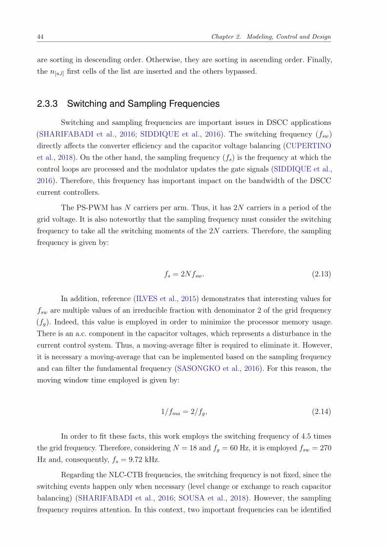
On the other hand, Fig 11 shows that for NLC-CTB the switching frequency is
the same as the reference signal. Although this example is for an unlimited capacitance,
according to the literature, the NLC-CTB operates with lower switching frequency than
PS-PWM. Therefore, the NLC-CTB tends to have lower switching losses and less stresses
on the power devices during the DSCC operation (SHARIFABADI et al., 2016; SOUSA et
al., 2018).
46 Chapter 2. Modeling, Control and Design
0
0.5
1
Sig
nal
s
0
0.5
1
Gat
e si
gn
al
ωnt0 2π 4π 6π
0 2π 4π 6π
Figure 11 – Operation of NLC-CTB (SOUSA et al., 2018).
2.4 Design
This work follows the design proposed in (CUPERTINO et al., 2018). In addition, a
15 MVA DSCC-STATCOM with line voltage of 13.8 kV at the Point of Common Coupling
(PCC) is considered .
In order to define the maximum dc-link voltage, in the design, it is considered:
• Variations in the grid voltage (∆Vg) of 5 %;
• STATCOM output impedance (Xeq = Xg + 0.5Xa) of 14 %, with a variation of 5 %;
• Effective dc-link voltage with 10 % of maximum ripple and a constant error of 3 %
in steady-state.
Furthermore, the line voltage synthesized is given by (FUJII; SCHWARZER;
DONCKER, 2005):
Vs = (1 + ∆Vg)[1 + Xeq(1 + ∆Xeq)]Vg ≈ 1.2Vg, (2.17)
where Vg is the PCC line voltage. Moreover, the minimum value of Vdc is given by (FUJII;
SCHWARZER; DONCKER, 2005):
Vdc =2√
2
0.87√
3
Vs
λmmax
. (2.18)
where mmax is maximum modulation index considered 0.9994 and λ is the modulation
gain considered 1.15, due to the modulation employed with 1/6 pu of third harmonic
(CUPERTINO et al., 2018). Thus, Vdc = 28 kV is employed.

2.4. Design 47
The number of cells is determined by (CUPERTINO et al., 2018):
N =1
fus
Vdc
Vsvc
, (2.19)
where fus is the usage factor of the semiconductor devices considered and Vsvc is the
semiconductor device voltage class. In this work, fus = 0.475 and Vsvc = 3.3 kV are
employed. Thus, N = 18 is employed.
Regarding the semiconductor devices, the superior limit for the arm currents that
they should support is given by (CUPERTINO et al., 2018):
max(i[u,l]) ≈3
4In. (2.20)
where In is the grid current peak value at nominal condition given by:
In =
√2√3
Sn
Vg
, (2.21)
where Sn is the STATCOM nominal power. Additionally, the rms value of arm current is:
i[u,l],rms ≈√
3
4In. (2.22)
Considering Sn = 15 MVA and Vg = 13.8 kV, max(i[u,l]) = 665.6 A and i[u,l],rms =
384.3 A. Therefore, in this work, an ABB IGBT module part number 5SND 0500N 330300
of 3.3 kV-500 A is employed.
Regarding the cell capacitance, its minimum value is given by (ILVES et al., 2014):
C =2NEnom
V 2dc
, (2.23)
where Enom is the minimum value of the nominal energy storage per arm, which is given
by:
Enom =SnWconv
6. (2.24)
where Wconv is the energy storage requirement. The literature suggests energy storage
requirement of 40 kJ/MVA (ILVES et al., 2014; CUPERTINO et al., 2018). For this
energy storage requirement, it is considered modulation with 1/6 third harmonic and
cell capacitor voltage ripple of 10%, perfectly balanced and close to the average voltage.
Therefore, C = 4.5 mF is employed.

48 Chapter 2. Modeling, Control and Design
The arm inductance is computed based on two criteria. In order to avoid reso-
nance, the arm inductance should satisfy the following expression (ILVES et al., 2012;
CUPERTINO et al., 2018):
LaC >5N
48ω2n
. (2.25)
where ωn is the angular grid frequency. In addition, in order to limit fault current, La
should satisfy:
La =Vdc
2α, (2.26)
where α (kA/s) is the maximum current rise rate. In order to fulfill these demands, this
work employs La = 0.15 pu (CUPERTINO et al., 2018). Thus, La = 5.1 mH is employed.
2.5 Dynamic Response
In order to demonstrate the dynamic behavior of the DSCC-STATCOM designed,
simulations were performed in PLECS environment. Tab. 3 presents the DSCC-STATCOM
parameters employed.
Table 3 – DSCC-STATCOM Parameters.
Parameter Value
Pole to pole dc voltage (Vdc) 28 kVRated power (Sn) 15 MVAGrid voltage (Vg) 13.8 kVGrid frequency (fg) 60 HzTransformer inductance (Lg) 1.35 mH (0.04 pu)Transformer X/R ratio 18
Arm inductance (La) 5.1 mH (0.15 pu)Arm resistance (Ra) 0.065 Ω (0.005 pu)Cell Capacitance for 40 kJ/MVA (C) 4.5 mFNumber of cells (N) 18 per armNominal cell voltage (v∗
avg) 1.56 kV
Switching frequency (fsw) 270 Hz
In addition, the controller parameters are shown in Tab. 4. The proportional integral
controllers are discretized by Tustin method, while the proportional resonant controllers
are discretized by Tustin with prewarping method. In order to analyze the converter
inductive and capacitive operation, the reactive power profile of Fig. 12 is employed. The
base values of 15 MVA and 13.8 kV are employed.
Fig. 13 (a) shows the reactive power injected/absolved by the DSCC-STATCOM.
For both modulation strategies, the reactive power response follows the reactive power

2.5. Dynamic Response 49
Table 4 – Parameters of the controllers.
Parameter Value
Sampling frequency (fs) 9.72 kHzProportional gain of average control (kp,avg) 8.39 Ω−1
Integral gain of average control (ki,avg) 143.9 Ω−1/sProportional gain of grid current control (kp,g) 6.3 Ω
Resonant gain of grid current control (kr,g) 1000 Ω/sProportional gain of circulating current control (kp,z) 1.3 Ω
Resonant gain of circulating current control (kr,z) 1000 Ω/sCirculating current LPF cut-off frequency (ωc) 8 HzProportional gain of individual balancing control (kb) 0.0004 V −1
Moving average filter frequency (fma) 30 Hz
Time (s)
-1
0
1
Q(p
u)
Capacitive
Operation
Inductive
Operation
0.5 1 1.5 2 2.5 3
0
Figure 12 – Reactive power profile.
profile with low absolute error, as observed in Fig. 13 (b). In addition, PS-PWM presents
lower oscillations in the reactive power response. Indeed, the absolute error between the
reactive power reference and reactive power measured is predominantly lower for PS-PWM.
Fig. 14 shows the grid current. As observed in Fig. 14 (a) and (d), for both
modulation strategies, the grid current follows the reactive power profile. In addition, Fig.
14 (b), (c), (e) and (f) show in detail the grid current in capacitive and inductive operation
condition and the respective THD. In terms of THD, PS-PWM presents lower values than
NLC-CTB for both operation conditions. In fact, this is explained due to the NLC-CTB
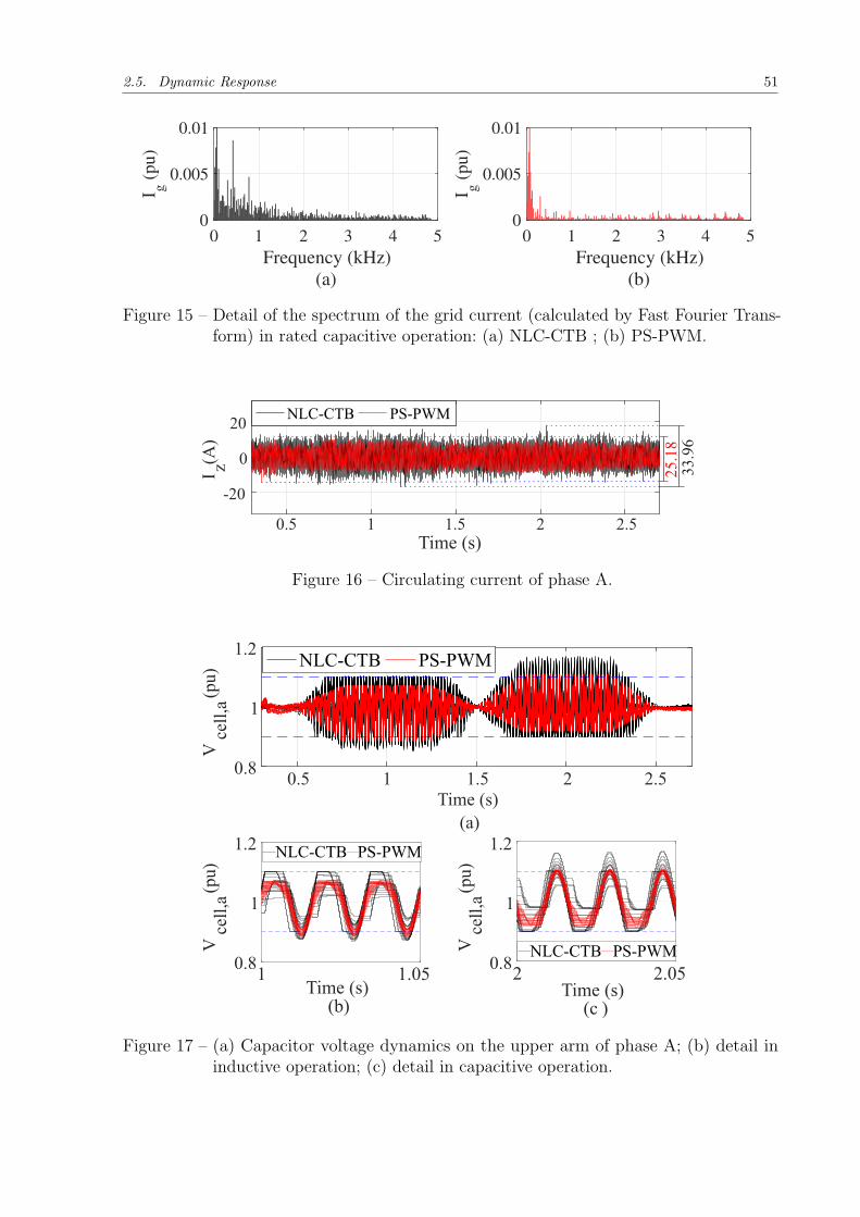
higher harmonic content when compared to PS-PWM, as shown in Fig. 15.
In terms of circulating current, the dynamic responses are presented in Fig. 16.
In accordance with previous results, PS-PWM presents lower oscillations, since it has
maximum variation of 25.18 A, while NLC has maximum variation of 36.96 A.
Fig. 17 presents the cell capacitor voltages. The dashed lines indicate the 10 %
range of voltage ripple. As observed in Fig. 17 (a), in rated inductive operation (0.75 s
to 1.25 s), both strategies respect the upper 10 % voltage limit and disrespect the lower
10 % voltage limit. On the other hand, in rated capacitive operation (1.75 s to 2.25 s),
both strategies respect the lower limit and disrespect the upper limit. Moreover, in Fig.

50 Chapter 2. Modeling, Control and Design
0.5 1 1.5 2 2.5
(a)
-1
0
1
Q (
pu
)
NLC-CTB PS-PWM
0.5 1 1.5 2 2.5
Time (s)
(b)
-0.1
0
0.1
Ab
solu
te e
rro
r (p
u)
NLC-CTB PS-PWM
Figure 13 – Reactive power response.
0.5 1 1.5 2 2.5
(a)
-1000
0
1000
I g(A
)
0.5 1 1.5 2 2.5
Time (s)
( )d
-1000
0
1000
I g(A
)
1 1.01
( )b
1 1.01
Time (s)
( )e
( )c
( )f
THD = 1.46% THD = 1.61%
THD = 0.53%THD = 0.52%
Figure 14 – Grid current: (a) NLC-CTB dynamic; (b) detail in rated inductive operationemploying NLC-CTB; (c) detail in rated capacitive operation employing NLC-CTB; (d)PS-PWM dynamic; (e) detail in rated inductive operation employingPS-PWM; (f) detail in rated capacitive operation employing PS-PWM.
17 (b) and (c) is noted that NLC-CTB exceeds more the voltage limits than PS-PWM,
presenting a higher spreading among the individual cell voltages.
2.5. Dynamic Response 51
0 1 2 3 4 5
Frequency (kHz)
(a)
0
0.005
0.01
I g (
pu)
0 1 2 3 4 5
Frequency (kHz)
(b)
0
0.005
0.01
I g (
pu)
Figure 15 – Detail of the spectrum of the grid current (calculated by Fast Fourier Trans-form) in rated capacitive operation: (a) NLC-CTB ; (b) PS-PWM.
Time (s)
-20
0
20
I z(A)
NLC-CTB PS-PWM
33.9
62
5.1
8
0.5 1 1.5 2 2.5
Figure 16 – Circulating current of phase A.
Time (s)
0.8
1
1.2
Vce
ll,a
(pu) NLC-CTB PS-PWM
Time (s)
NLC-CTB PS-PWM
Time (s)
NLC-CTB PS-PWM
(a)
0.8
1
1.2
Vce
ll,a
(pu)
0.8
1
1.2
Vce
ll,a
(pu)
1 1.05 2 2.05
(b) (c )
1 1.5 2 2.50.5
Figure 17 – (a) Capacitor voltage dynamics on the upper arm of phase A; (b) detail ininductive operation; (c) detail in capacitive operation.

52 Chapter 2. Modeling, Control and Design
2.6 Chapter Conclusions
In this chapter the topology, controls, modulation strategies and design of DSCC-
STATCOM were presented. In addition, the dynamic response of the converter was analyzed
for both modulation strategies. The results shown satisfactory response of reactive power,
grid current and circulating current, demonstrating effectiveness of the controls employed.
Nevertheless, the cell capacitor voltage did not respect the 10% voltage tolerance. This
fact demonstrates that the energy storage requirement calculated may not be sufficient
to maintain individual voltages in the tolerance range. Indeed, the design was made
considering individual cell capacitor voltages perfectly balanced and close to the cell
average voltage. For this reason, in the next chapter the energy storage requirement for
each modulation strategy is evaluated.

53
3 Energy Storage Requirements
3.1 Spreading Factor
The results of Chapter 2 demonstrated that the traditional cell capacitor design is
not enough to guarantee a cell capacitor voltage ripple respecting the tolerance of 10 %
regarding to cell voltage reference. Indeed, the design proposed by (ILVES et al., 2014;
CUPERTINO et al., 2018) considers perfectly balanced capacitor voltages. Nevertheless,
due to the limited switching frequency, a spread is expected in the instantaneous capacitor
voltages, as observed in Fig. 18. The dashed lines indicate the 10 % range of voltage ripple.
0.4 0.42 0.44
Time (s)
(a)
0.8
0.9
1
1.1
1.2
Vce
ll,a
(pu)
210 Hz Avg.
0.4 0.42 0.44
Time (s)
(b)
0.8
0.9
1
1.1
1.2V
cell
,a (
pu)
570 Hz Avg.
Figure 18 – Upper arm capacitor voltages for different switching frequencies: (a) 210 Hz;(b) 570 Hz. Operating Conditions: DSCC Parameters of Tab. 3, rated capacitivereactive power, 40 kJ/MVA of energy storage requirement and modulationstrategy PS-PWM.
As observed in Fig. 18 (a), although the average capacitor voltage (Avg.) is within
the 10 % range, the instantaneous capacitor voltage ripple reaches values higher than 10
%. However, the capacitor voltages could present different behavior for other switching
frequencies, as illustrated in Fig. 18 (b). This indicates that the evaluation of the energy
storage requirement depends on the capacitor voltage spreading.
Aiming to quantify the spreading for a given modulation strategy, this work defines
the spreading factor (Ke). This factor is computed per arm and quantifies the difference
between the capacitor voltages and the average value. Accordingly:
Ke =
N −N∑
k=1
ρi
N, (3.1)

54 Chapter 3. Energy Storage Requirements
where N is the number of cells per arm and ρi is the Pearson correlation coefficient of the
ith cell capacitor voltage vcell,i, given by:
ρi =cov(vcell,i, vavg)
σavgσcell,i
. (3.2)
where the total average voltage is given by:
vavg =
∑Nk=1 vcell,i
N. (3.3)
The function cov refers to the covariance of vcell,i and vavg, while σavg and σcell,i are
the standard deviations. Based on (3.1), if the capacitor voltages are perfectly balanced,
vavg = vcell,i, ρi = 1 and the spreading factor is Ke = 0. This factor is useful to compare
the capacitor voltage balancing capability of different modulation strategies.
Fig. 19 exemplifies the correlation between individual cell voltage and arm cell
average voltage. As observed, in ideal case of perfectly balanced capacitor voltages and
Ke = 0, the vcell per vavg would produce a straight line of unitary coefficient. Nevertheless,
it is observed that for the case of 210 Hz the points are further of the ideal case than for
570 Hz. This result is consistent with the spreading factor computed in the cases, in which
for 210 Hz and 570 Hz Ke is 0.0453 and 0.0027, respectively.
0.9 0.95 1 1.05 1.1
Vavg
(pu)
0.9
0.95
1
1.05
1.1
Vce
ll (
pu)
210 Hz
570 Hz
Avg.
Figure 19 – Correlation between individual cell voltage and arm cell average voltage.Operating Conditions: DSCC Parameters of Tab. 3, rated capacitive reactivepower, 40 kJ/MVA of energy storage requirement and modulation strategyPS-PWM.
3.2 Modulation Strategy and Spreading Factor
Different modulation strategies can have different capacitor voltage balancing
capability and, consequently, they can demand different energy storage requirements. For

3.2. Modulation Strategy and Spreading Factor 55
this reason, the spreading factor and the energy storage requirement from NLC-CTB and
PS-PWM are evaluated.
In addition, simulations were implemented in PLECS environment. The parameters
employed in these simulations are the same of Tab. 3.
Fig. 20 presents the spreading factor and the energy storage requirement for
different values of switching frequency for PS-PWM and different sampling frequencies for
NLC-CTB. For this analysis, it was employed as fsw, values of irreducible fraction with
denominator 2 of the grid frequency (fs/(2Nfg)).
Fig. 20 (a) compares the spreading factors of NLC-CTB and PS-PWM strategies
for the energy storage of 40 kJ/MVA. As observed, when the switching frequency is
increased, the spreading factor of PS-PWM is reduced. For NLC-CTB, the spreading factor
is always larger than PS-PWM in this frequency range. Furthermore, the spreading factor
of NLC-CTB is not related with the sampling frequency.
5/2
(a)
(b)
0
0.05
0.1
0.15
Ke
NLC-CTB PS-PWM
40
60
80
Wco
nv
(kJ/
MV
A) NLC-CTB PS-PWM
fs
(kHz)
W = 6 kJ/MVA5conv
W = 4 kJ/MVA5conv
5.4 7.56 9.72 11.88 14.04 16.2 18.36 20.52
5.4 7.56 9.72 11.88 14.04 16.2 18.36 20.52
fs g/( )2Nf
7/2 11/29/2 13/2 15/2 17/2 19/2
W 40conv= kJ/MVA
Figure 20 – Comparison of capacitor balancing performance of the studied modulationstrategies: (a) Spreading factor, considering Wconv = 40 kJ/MVA; (b) Energystorage requirements.
As a consequence of a non null spreading factor, the cell capacitance must be

56 Chapter 3. Energy Storage Requirements
increased in order to guarantee that all capacitor voltage ripples are contained within
the 10 % range. Fig. 20 (b) shows the necessary energy storage requirement for both
modulation strategies. As observed, the curves follow the same pattern of Fig. 20 (a).
In addition, NLC-CTB presents higher energy storage requirements than the PS-PWM
strategy.
The switching and sampling frequencies, previously defined, are 270 Hz and 9.72
kHz, respectively. For the selected operating frequencies, Wconv = 45 kJ/MVA for PS-PWM
and Wconv = 65 kJ/MVA for NLC-CTB. Thus, employing the Eq. (2.23) and Eq. (2.24),
the cell capacitances obtained are 5.17 mF and 7.46 mF, for PS-PWM and NLC-CTB,
respectively.
Regarding the capacitor voltage balancing capability, Fig. 21 shows the cell capacitor
voltages considering identical capacitances in all cells. As observed in Fig. 21 (a), during
the inductive operation (0.75 s to 1.25 s) and capacitive operation (1.75 s to 2.25 s), both
strategies respect the upper and lower 10 % voltage limits. Moreover, in Fig. 21 (b) and
(c) is noted that NLC-CTB still presents a higher spreading among the individual cell
voltages.
1 1.05Time (s)
0.8
1
1.2
Vce
ll,a
(pu
) NLC-CTB PS-PWM
(b)
2 2.05Time (s)
0.8
1
1.2
Vce
ll,a
(pu
) NLC-CTB PS-PWM
(c)
Time (s)
0.8
1
1.2
Vce
ll,a
(pu
) NLC-CTB PS-PWM
0.5 1 21.5 2.5
( )a
Figure 21 – (a) Capacitor voltage dynamics on the upper arm of phase A; (b) detail ininductive operation; (c) detail in capacitive operation.
Regarding the spreading factor, as observed in Tab. 5, the NLC-CTB presents
values approximately 60 % higher than PS-PWM. This result is in accordance with the
visual inspection of Figs. 21 (b) and (c).
Some commercial capacitors can have 10 % tolerance in the capacitance. Therefore,
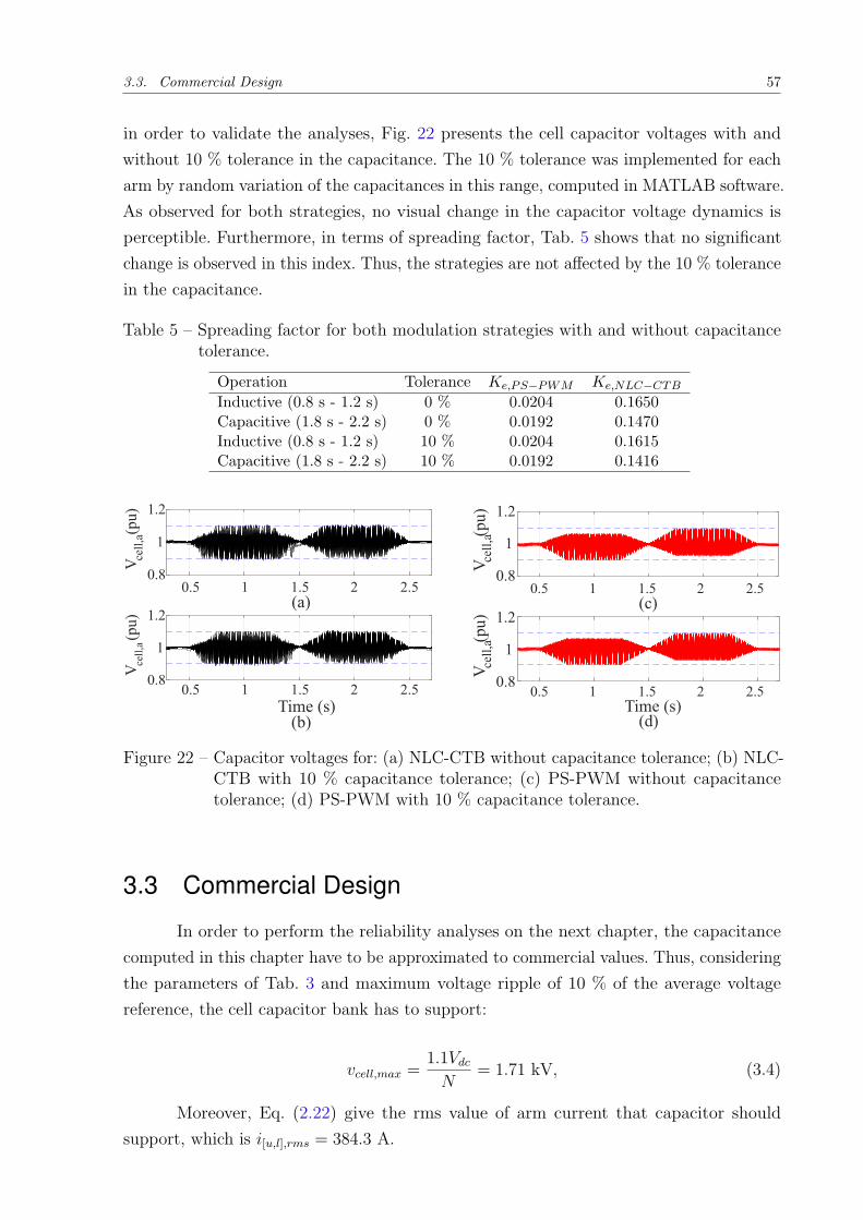
3.3. Commercial Design 57
in order to validate the analyses, Fig. 22 presents the cell capacitor voltages with and
without 10 % tolerance in the capacitance. The 10 % tolerance was implemented for each
arm by random variation of the capacitances in this range, computed in MATLAB software.
As observed for both strategies, no visual change in the capacitor voltage dynamics is
perceptible. Furthermore, in terms of spreading factor, Tab. 5 shows that no significant
change is observed in this index. Thus, the strategies are not affected by the 10 % tolerance
in the capacitance.
Table 5 – Spreading factor for both modulation strategies with and without capacitancetolerance.
Operation Tolerance Ke,P S−P W M Ke,NLC−CT B
Inductive (0.8 s - 1.2 s) 0 % 0.0204 0.1650
Capacitive (1.8 s - 2.2 s) 0 % 0.0192 0.1470
Inductive (0.8 s - 1.2 s) 10 % 0.0204 0.1615
Capacitive (1.8 s - 2.2 s) 10 % 0.0192 0.1416
(a)
0.8
1
1.2
Vce
ll,a
(pu
)
(b)Time (s)
0.8
1
1.2
Vce
ll,a
(pu
)
0.5 1 1.5 2 2.5
0.5 1 1.5 2 2.5
0.8
1
1.2
Vce
ll,a(p
u)
0.8
1
1.2
Vce
ll,a(p
u)
( )c0.5 1 1.5 2 2.5
( )d
0.5 1 1.5 2 2.5Time (s)
Figure 22 – Capacitor voltages for: (a) NLC-CTB without capacitance tolerance; (b) NLC-CTB with 10 % capacitance tolerance; (c) PS-PWM without capacitancetolerance; (d) PS-PWM with 10 % capacitance tolerance.
3.3 Commercial Design
In order to perform the reliability analyses on the next chapter, the capacitance
computed in this chapter have to be approximated to commercial values. Thus, considering
the parameters of Tab. 3 and maximum voltage ripple of 10 % of the average voltage
reference, the cell capacitor bank has to support:
vcell,max =1.1Vdc
N= 1.71 kV, (3.4)
Moreover, Eq. (2.22) give the rms value of arm current that capacitor should
support, which is i[u,l],rms = 384.3 A.

58 Chapter 3. Energy Storage Requirements
Moreover, considering the case of higher cell capacitance (7.46 mF for NLC-CTB)
and Electronicon Film Capacitors (ELECTRONICON, 2015) two possibilities of capacitor
banks were analyzed:
• Case 1: 7 capacitors in parallel, in which each capacitor has rated voltage (Vnom) of
1.8 kV;
• Case 2: 2 capacitors in series replicated 5 times in parallel, in which each capacitor
has rated voltage of 1.1 kV.
Tab. 6 presents the comparison between these cases. In this table, the cost of
the capacitors are approximated from the current market prices considering 150 e/kJ
(ENGEL et al., 2015). In this context, the energy storage per cell is given by:
Ecell =NcapCNV 2
nom
2, (3.5)
where Ncap is the number of capacitors in the capacitor bank. Thus, in terms of cost the
Case 1 is more interesting.
Table 6 – Capacitor bank design evaluation.
Parameter Case 1 Case 2
Individual capacitance CN (mF) 1.06 2.90
Rated voltage Vnom (kV) 1.8 1.1Maximum current per capacitor (A) 120 120Number of capacitors Ncap 7 10
Energy storage per cell Ecell (kJ) 12.02 17.55
Cost (e/cell) 1803.06 2631.75
For this reason, the realization of the cell capacitance is based on Electronicon Film
Capacitors, part number E50.S34-115NT0, of 1.06 mF and 1.8 kV-120 A. Therefore, for
NLC-CTB, 7 of these capacitors are used in parallel, resulting in 7.42 mF. Analogously,
for the PS-PWM, 5 of these capacitors are used in parallel, resulting in 5.3 mF. Despite
the fact that the NLC-CTB capacitance value is smaller than previously stated, this
approximation is made to avoid oversizing.
Finally, three different case studies have been defined for the analyses on the next
chapter:
• PS-5C: PS-PWM with cell capacitance of 5.3 mF;
• PS-7C: PS-PWM with cell capacitance of 7.42 mF;
• NLC-7C: NLC-CTB with cell capacitance of 7.42 mF.

3.4. Chapter Conclusions 59
3.4 Chapter Conclusions
In this chapter, the modulation strategy impact on the energy storage requirements
of a DSCC-STATCOM was analyzed. Furthermore, the spreading factor index was intro-
duced in order to quantify the capacitor voltage balancing capability of each modulation
strategy.
As observed, while the spreading factor of PS-PWM decreases when the switching
and sampling frequencies increase, for NLC-CTB, the spreading factor is higher than
for PS-PWM and it is not related with its sampling frequency. Consequently, for a non
null spreading factor, the cell capacitance must be increased in order to guarantee that
all capacitor voltage ripples are contained within the 10% range. As a result, NLC-CTB
presents higher energy storage requirements than the PS-PWM strategy.
In terms of capacitor voltage, for the computed capacitance values, both strategies
comply with the upper and lower 10% voltage limits. However, NLC-CTB presents higher
spreading factor under capacitive and inductive reactive power conditions.
Finally, the capacitances computed were approximated to commercial values and
three different case studies were defined in terms of energy storage requirements and
modulation strategies. Furthermore, these case studies are employed in the reliability
analyses on the next chapter which are focused on the lifetime of semiconductor devices
(i.e. IGBTs and diodes) and capacitors.


61
4 Reliability of a DSCC-STATCOM
4.1 Introduction
In general definition, reliability is the ability of an item to perform a required
function under stated conditions for a stated period of time (IEEE. . . , 2010). In addition,
this term has been drawing attention in recent years, mainly, related with power electronics
systems. In fact, the power electronics system elements have become crucial constituents
in the further development of emerging application fields as lighting, more-electric aircraft
and medical systems (FALCK et al., 2018).
Nevertheless, power electronics systems include a large number of fragile elements,
semiconductors, capacitors, magnetics, controllers, sensors and auxiliary devices (FALCK
et al., 2018). Among the power electronic elements, semiconductor devices and capacitors
are classified as the components most likely to fail. Moreover, the failure of a single part
causes downtime and maintenance cost (FALCK et al., 2018). Therefore, since the DSCC
topology can have hundreds/thousands of components, reliability concerns are presented
in the converter design (ALHARBI; BHATTACHARYA; YOUSEFPOOR, 2017).
On the context of reliability evaluation, the analysis are divided into three periods
of failure: early failure period, due to manufacturing defects; constant failure period in
the useful life of the device; and aging failure period, due to degradation processes of the
component (wear-out failure) (RICHARDEAU; PHAM, 2013). Fig. 23 presents the classic
bathtub failure curve with the component failure periods. As observed in Fig. 23, the
failure rate increases exponentially in the wear-out failure period due to the cumulative
damage (FALCK et al., 2018).
Operation time hours, , etc.( years )
Fai
lure
rat
eλ(t
)
Constant failure periodWear-out failureEarly failure
period period
Figure 23 – Bathtub failure curve divided into three periods.
In this context, the design of the converter must ensure that wear-out failures will
not be an issue during the converter operation. Moreover, the wear-out failure can be
predicted at a certain level, if the degradation mechanism is known. For this reason, this
work analyzes this period.

62 Chapter 4. Reliability of a DSCC-STATCOM
Regarding the wear-out failure, several works propose methodologies in order to
estimate the lifetime of components considering this period (FALCK et al., 2018). In
addition, the temperature is one of the main stress factors. For this reason, thermal models
are usually employed on the lifetime evaluation.
Additionally, for semiconductor devices, the stress factors are related to the junction
and case temperature. These temperatures are proportional to the internal losses and,
consequently, thermal cycling. Besides, semiconductor devices are formed by different
materials, as illustrated for an IGBT module in Fig. 24. Thus, the thermomecanical stress
produced by the thermal cycling results in degradation of the solders and bondwires.
Furthermore, the most critical joins of an IGBT module are bondwire, base plate solder,
conductor solder and chip solder, as shown in Fig. 24 (ABB, 2014).
Bondwire
Heatsink
Base Plate
Chip Solder
Diode IGBT
Base PlateSolder
ThermalGrease
ConductorSolder
Conductors
Figure 24 – Schematic of an IGBT module (Adapted from ABB (2014)).
Regarding the capacitors, the hotspot temperature and the voltage ripple are the
stress factors in wear-out failure. Besides, in high voltage levels Metallized Polypropy-
lene Film Capacitors are usually employed. In this capacitor technology, the thermal
stress produce chemical degradation of the film, leading to component failure (WANG;
BLAABJERG, 2014).
Lastly, different modulation strategies can generate different thermal stress, resulting
in different lifetimes. Based on that, this chapter perform reliability analyses, focused
in the wear-out failure period, with the purpose to evaluate the impact of modulation
strategies on the lifetime of a DSCC-STATCOM.
4.2 Lifetime Evaluation
4.2.1 Semiconductor Devices
The long-term lifetime evaluation flowchart of semiconductor devices employed in
this work is shown in Fig. 25. Furthermore, an ABB IGBT part number 5SND 0500N330300
of 3.3 kV-500 A is employed.

4.2. Lifetime Evaluation 63
Power LossesLook-up Table
ThermalModel
Rainflow
Tj
T[j,c]m ΔTj,cton
Ta
Q
Plosses,SDMissionProfiles
Tj
Nf
Miner’s Rule
LC
Tc
LifetimeModel
ton1
Tc1Tc2 Tc3
ton1
Tc1Tc2 Tc3
ton1
Tc1Tc2 Tc3Nf
ΔTj,c
ton1
Tc1 Tc2 Tc3
ni
ΔT (°C)j T (°C)j
Nu
mb
er o
f C
ycl
es
Tj
Multi-layer Cauer Z j-c
Z c-h Z h-a
Plosses
Multi-layer Foster Z j-c
Plosses
Tc Th Ta
>
>
>>
>
>
Figure 25 – Lifetime evaluation flowchart of semiconductor devices.
As observed in Fig. 25, mission profiles of reactive power (Q) and ambient temper-
ature (Ta) are employed. In addition, the power losses in the devices are obtained from
look-up table based on the datasheet curves, as follows:
• The conduction losses of the diodes were obtained employing the curves of dc forward
current as a function of the forward voltage;
• The switching losses of the diodes were obtained from the curves of switching losses
as a function of the dc forward current;
• The conduction losses of the IGBTs were obtained employing the curves of dc
collector current as a function of the collector-emitter voltage;
• The switching losses of the IGBTs were obtained from the curves of switching losses
as a function of the dc collector current.
Additionally, an important feature is the power losses dependence of the temperature.
In fact, the information above mentioned is obtained from the datasheet contents for the
temperatures of 25C, 125C and 150C.
Moreover, the hybrid thermal model proposed by (TU; XU, 2011b; MA et al., 2016)
is employed in order to estimate the junction temperature (Tj) and case temperature (Tc),

64 Chapter 4. Reliability of a DSCC-STATCOM
as illustrated in Fig. 26. This model is based on Foster and Cauer models (ABB, 2013a).
In addition, this work considers one heatsink per cell.
Tj
Multi-layer Cauer
Z c-hZ h-a
Multi-layer Foster
TcTheat
Ta
Tc
Z j-c,foster
Z j-c,cauerPlosses
S1S2
D1D2
Plosses
Look-upLosses
Q
Z w-a
Figure 26 – Hybrid thermal model based on Foster and Cauer models.
Tab. 7 presents the Foster (Zj−c,foster) and case to heatsink (Zc−h) impedances
from the datasheet (ABB, 2013b).
Table 7 – Foster and case to heatsink parameters of the thermal model (ABB, 2013b).
Device Parameter Zj−c,foster Zc−h
IGBTRi (K/kW) 17.56 4.12 1.922 1.896 0.024
τi (ms) 207.4 30.1 7.55 1.57 -
DiodeRi (K/kW) 34.2 8.56 3.84 3.84 0.048
τi (ms) 203.6 30.1 7.53 1.57 -
Furthermore, Tab. 8 presents the Cauer parameters (Zj−c,cauer) based in the Foster
parameters, which were converted by the software PLECs.
Table 8 – Cauer parameters of the thermal model.
Device Parameter Zj−c,cauer
IGBTRi (K/W) 0.0035 0.005 0.0069 0.010Ci (J/K) 0.5941 2.156 4.279 11.02
DiodeRi (K/W) 0.0071 0.010 0.014 0.02Ci (J/K) 0.2933 1.063 2.104 5.727
Regarding the heatsink parameters (i.e. thermal resistance and capacitance), a sim-
plified heatsink model proposed by (ASIMAKOPOULOS et al., 2015) for power converter
was employed. This model considers a uniform temperature profile throughout the power
devices base plate and heatsink volume. The heatsink geometry has a simple rectangular
cross-section, and it is approximated by a simple orthogonal brick (ASIMAKOPOULOS
et al., 2015; JuNIOR et al., 2019). In such conditions, the heatsink parameters can be
computed by:
Rh−w =dh
λhAh
, (4.1)

4.2. Lifetime Evaluation 65
Ch−w = chρhdhAh, (4.2)
where dh is the heatsink thickness, λh is the thermal conductivity of the heat sink material,
Ah is the heatsink surface area, ch is the specific heat capacity and ρh is the material
density. In addition, this work considers an aluminum heatsink.
Additionally, it is necessary to calculate the thermal resistance representing the
water cooling system in order to improve the heat exchange from the heat sink to the
ambient. This resistance can be calculated by (JuNIOR et al., 2019):
Rw−a =1
hcAh
, (4.3)
where hc is the water flow convection coefficient which can range from 50 to 2500 W/(m2K),
depending on the speed and type of water flow, temperature dependent properties, and
pressure (JuNIOR et al., 2019). In this work, the necessary value was determined through
thermal simulations, which were carried out in order to maintain the junction and case
temperatures within the limits for the worst conditions (for the selected power modules,
120 C in the junction and 80 C in the device case). Therefore, hc = 575 W/(m2K) is
employed, which is a reasonable value into the range.
The parameters employed to calculate the heatsink and water cooling impedances
are shown in Tab. 9. The respective impedances calculated with these parameters are
presented in Tab. 10.
Table 9 – Parameters of the heatsink and water cooling impedances.
Parameter Value
dh 3 cmλh 238 W/(mC)Ah 0.0182 m2
ch 900 J/(kgC)ρh 2700 kg/m3
hc 575 W/(m2K)
Table 10 – Parameters of the heatsink and water cooling impedances.
Parameter Value
Rh−w 0.007C/WCh−w 1327 J/CRw−a 0.095 K/W
Once the temperatures Tj and Tc are obtained from the thermal model, the next
step is to apply then in lifetime model. However, this model requires regular data series
with constant average values (T[j,c]m), peak (∆Tj,c), heating time (ton) and number of

66 Chapter 4. Reliability of a DSCC-STATCOM
cycles (ni). In fact, the main failure mechanism is related to the thermal cycling which is
obtained from these regular data series (SANGWONGWANICH et al., 2018b).
Therefore, in order to apply the irregular profiles of Tj and Tc to the lifetime
model, which is based on the empirical data, a cycle counting algorithm is needed for the
thermal cycling interpretation. In this work, a rainflow counting algorithm is employed to
decompose the irregular profile into several regular cycles according to the cycle amplitude,
average value and the cycle period. Thus, after the rainflow, the regular information is
applied to the lifetime model and the lifetime of the semiconductor device can then be
evaluated (SANGWONGWANICH et al., 2018b).
Regarding the lifetime model, the number of cycles to failure (Nf) is calculated
using look-up tables provided by Application Note of ABB for Hi-Pak power modules
(ABB, 2014). This application note employs Weibull distribution. In addition, the results of
this distribution are used to determined the B10 lifetime which is described as the number
of cycles where 10 % of the modules of a population fail. Moreover, the lifetime models in
the application note are based on the Coffin-Manson law and fatigue of the joints due to
plastic deformation (ABB, 2014).
Furthermore, the application note presents B10 lifetime for four critical joins of the
IGBT module: bondwire, base plate solder, conductor solder, and chip solder (ABB, 2014).
The chip, base plate and conductor solders are dependent of the cycle period. In
this context, for the model of chip solder, Tjm, ∆Tj and ton are employed. For the base
plate and conductor solders, Tcm, ∆Tc and ton are employed. In addition, the lifetime of
base plate and conductor solders are described by the same model (ABB, 2014).
On the other hand, the model of the bondwire is independent of the cycle period,
due to this model assume that immediate plastic deformation leads to fatigue instead of
time dependent creep. For this reason, Tjm, ∆Tj are employed in this model (ABB, 2014).
Subsequently, with the Nf values of each model, the Life Consumptions (LCs) of
the semiconductor devices are calculated separately for each model by using the Miner’s
rule (MINER, 1945), as follows:
LC =∑
i
ni
Nf,i
, (4.4)
where ni is the ith number of cycles obtained from the rainflow algorithm and Nf,i is the
ith number of cycles to failure.
4.2.2 Cell Capacitor
The capacitor lifetime evaluation flowchart is shown in Fig. 27. The capacitor can be
modeled as an ideal capacitor (C) in series with an Equivalent Series Resistor (RESR) and

4.2. Lifetime Evaluation 67
an Equivalent Series Inductor (LESL). RESR performs the power dissipation. In addition,
RESR is frequency-dependent and can be calculated as follows (ELECTRONICON, 2014;
YANG et al., 2014):
RESR(fi) = Rs +tan(δ0)
2πfi × CN
, (4.5)
where Rs is the equivalent series resistance, fi is the frequency, tan(δ0) is the dielectric
dissipation factor and CN is the rated capacitance. According to the datasheet, Rs = 0.82
mΩ, tan(δ0) = 2 × 10⁻⁴ and CN = 1.06 mF (ELECTRONICON, 2014).
Rth
Th
+
-
+-
C
RESR
LESL
ic
FFT
ic
ic,1
ic,2
ic,h
∑P (f )losses h
0 0.5 1
Reactive Power (pu)
0
0.5
1
1.5
2
2.5
Lo
sses
(W
)
Q
Ta
ThermalModel
Plosses,C
Lifetime Model
Th
vc
Lf
Miner’s RuleLC
+
-
vc
Figure 27 – Lifetime evaluation flowchart of the capacitor.
Due to RESR frequency dependence, the Fast Fourier Transform (FFT) is applied
in the capacitor current. Subsequently, the power losses can be calculated by (ELEC-
TRONICON, 2014; YANG et al., 2014):
Plosses,C =∑
h=1
I2c,i × RESR(fi), (4.6)
where Ic,i is the amplitude of the capacitor current for the frequency fi. The capacitor
current is sampled at 97.2 kHz in a period of 2 s, with frequency resolution of 0.5 Hz. This
resolution was chosen due to the variations in the capacitor current of the NLC-7C. The
capacitor power losses look-up table is obtained by applying Eq. (4.6).
The hotspot temperature (Th) is given by (YANG et al., 2014):
Th = Plosses,CRth + Ta, (4.7)
where Rth is the thermal resistance of the capacitor given in the datasheet as 0.9 K/W.

68 Chapter 4. Reliability of a DSCC-STATCOM
According to (ELECTRONICON, 2014), the lifetime model of the capacitor is
given by:
Lf = L0 ×(
Vc
Vc,rated
)−n
× 2
(Th,rated−Th
7k
)
(4.8)
where Lf is the time-to-failure, L0 is rated lifetime, Vc,rated and Th,rated are the rated values
of the capacitor voltage and hotspot temperature obtained in the datasheet. In addition,
Vc and Th are the capacitor voltage and hotspot temperature in which the capacitor is
operating. The parameters of the capacitor lifetime model are obtained from the datasheet
(ELECTRONICON, 2015) and given in Table 11.
Table 11 – Parameters of the Capacitor Lifetime Model (ELECTRONICON, 2014).
Parameter Value
L0 100000 hoursVc,rated 1.8 kVTh,rated 70Cn 8.8529k 0.9895
The capacitor LC is also calculated by using the Miner’s rule, as follows:
LC =∑
i
liLf,i
, (4.9)
where li is the operating time, according to the mission profile resolution and Lf,i is the
time-to-failure calculated from Eq. (4.8).
In lifetime evaluations of photovoltaic inverters, the capacitor voltage ripple is
usually neglected in the lifetime analysis (SANGWONGWANICH et al., 2018b). Indeed,
the capacitor voltage ripple is relatively low in this application. Consequently, its impact
on lifetime is lower than that of the temperature. Nevertheless, in DSCC applications, the
capacitor voltage usually presents ripple of ±10 %, relative to the voltage reference. Thus,
the capacitor voltage ripple might have some impact on lifetime.
Fig. 28 is based on simulations implemented in the PLECS environment, considering
the parameters of Tab. 3, the case study PS-5C and the injection of rated reactive power
(capacitive mode). Fig. 28 (a) illustrates three options of capacitor voltage to be considered
in the lifetime analysis: cell reference, arm cell average and individual cell. As observed,
the individual cell voltages have a spreading. In addition, the high number of cells increase
the computational effort for the lifetime evaluation. For this reason, the individual cell
voltages are not employed. Another option is the use of the reference voltage. However,
the voltage ripple is not taken into account. A trade-off is the use of the arm cell average
voltage.

4.2. Lifetime Evaluation 69
Nevertheless, when the arm cell average voltage is considered, a sampling frequency
must be defined. Fig. 28 (b) illustrates the sampling frequency effect on the voltage informa-
tion considered in the analyses. Thus, it is necessary to investigate the sampling frequency
that optimizes the computational work and remains the relevant voltage information for
the analyses.
0.4 0.41 0.42 0.43 0.44 0.45
0.9
1
1.1
Vc
(pu)
Ref. Avg. Ind.
0.4 0.41 0.42 0.43 0.44 0.45
Time (s)
0.9
1
1.1
Vc
(pu)
Ref. Avg. 800 Hz
( )a
( )b
Figure 28 – (a) Capacitor voltage considering the voltages of cell reference, arm averageand individual cell; (b) Capacitor voltage sampling. Operating Conditions:Parameters of Tab. 3, case study PS-5C and rated capacitive operation.
0 2 4 6 8 10 12
Sampling frequency (kHz)
0.7
0.8
0.9
1
1.1
Lf
(pu)
Capacitive Inductive Reference
δLf = 7.84%
Figure 29 – Individual capacitor lifetime considering the capacitor voltage as rated capaci-tive, inductive and the cell reference for different capacitor voltage samplingfrequencies. Operating Conditions: Parameters of Tab. 3 and 11, Th fixed at60C, case study PS-5C. Lifetime values normalized by the lifetime computedconsidering the cell reference voltage.
For this purpose, Fig. 29 presents the lifetime computed by different sampling
frequencies, considering capacitive and inductive rated operation voltage. As observed,
the lifetime remains almost constant when the sampling frequency is higher than 4 kHz.
Therefore, in the following analysis, the value employed is 4.02 kHz, once it is a multiple
integer of the grid frequency (60 Hz).
Moreover, Fig. 29 also presents the ripple effect on lifetime evaluation. As noted, the
use of the cell voltage reference can generate relative error (δLf ) of 7.84 % when compared to

70 Chapter 4. Reliability of a DSCC-STATCOM
the worst case of arm cell average voltage (during rated operation). This result demonstrates
the significant effect of cell capacitor voltage ripple on lifetime estimation.
4.2.3 Monte Carlo Based Reliability Evaluation
The lifetime evaluation methodologies previously presented consider an ideal case of
fixed time-to-failure in which all components fail at the same time. However, this considera-
tion is not realistic. Indeed, the lifetime models presented may vary due to the manufactur-
ing process, mission profile and lifetime model parameters (SANGWONGWANICH et al.,
2018a). In order to represent practical applications, Monte Carlo simulation is employed.
This method introduces parameter variations into the lifetime model (REIGOSA et al.,
2016). The Monte Carlo analysis flowchart is shown in Fig. 30.
Monte CarloSimulation Weibull Distribution
Translation intoEquivalent Static
Values
ΔTj,c
T[j,c]m
Nf
ton
Th
Vc
Lf
ΔT’j,c
T’[j,c]m
T ’h
Reliability Analysis
UnreliabilityfunctionSystem levelreliability
Componentslevel reliability
f(x)
Nf,1
Nf,n
Lf,1
Lf,n
3σ-1σ 1σ 2σ-2σ-3σ
X
Time (Year)
f(x) : Weibull PDF
Time (Year)
F(x): Weibull CDF
Bx
100%
x%
Figure 30 – Monte Carlo analysis flowchart.
In order to apply the Monte Carlo simulation, the parameter variations should be
introduced. However, this methodology employs distribution functions and the dynamic
parameters (T[j,c]m, ∆Tj,c and Th) cannot be easily modeled for their application. For
this reason, the dynamic parameters are converted into equivalent static values (T ′
[j,c]m,
∆T ′
j,c and T ′
h) which result in the same lifetime, when applied on the lifetime model
(SANGWONGWANICH et al., 2018a).
Subsequently, normal distribution with 5 % of standard deviation is applied in
T ′
[j,c]m, ∆T ′
j,c, T ′
h, n, k, L0 and Vc. Moreover, the Monte Carlo simulation with population
of 10.000 samples is carried out for each component using the lifetime models.
The lifetime yield for each sample is obtained from the simulation and fitted with
the Weibull distribution (f(x)), which is the probability density function (PDF) given by
(SANGWONGWANICH et al., 2018a):
f(x) =β
ηβxβ−1exp
−
(x
η
)β (4.10)
where x is the operation time, β is the shape parameter and η is the scale parameter.
Additionally, from the lifetime distribution, it is also obtained the component unre-
liability function (F (x)), which is a cumulative density function (CDF). F (x) represents
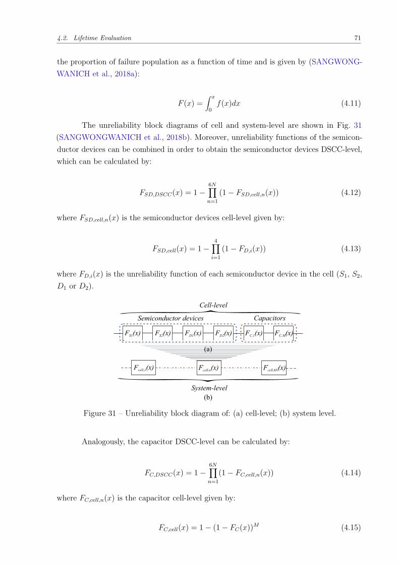
4.2. Lifetime Evaluation 71
the proportion of failure population as a function of time and is given by (SANGWONG-
WANICH et al., 2018a):
F (x) =∫ x
0f(x)dx (4.11)
The unreliability block diagrams of cell and system-level are shown in Fig. 31
(SANGWONGWANICH et al., 2018b). Moreover, unreliability functions of the semicon-
ductor devices can be combined in order to obtain the semiconductor devices DSCC-level,
which can be calculated by:
FSD,DSCC(x) = 1 −6N∏
n=1
(1 − FSD,cell,n(x)) (4.12)
where FSD,cell,n(x) is the semiconductor devices cell-level given by:
FSD,cell(x) = 1 −4∏
i=1
(1 − FD,i(x)) (4.13)
where FD,i(x) is the unreliability function of each semiconductor device in the cell (S1, S2,
D1 or D2).
F (x)S1 F (x)S2 F (x)D1 F (x)D2 F (x)C,1 F (x)C,M
F (x)cell,1 F (x)cell,n F (x)cell,6N
Semiconductor devices Capacitors
Cell-level
System-level
(b)
(a)
Figure 31 – Unreliability block diagram of: (a) cell-level; (b) system level.
Analogously, the capacitor DSCC-level can be calculated by:
FC,DSCC(x) = 1 −6N∏
n=1
(1 − FC,cell,n(x)) (4.14)
where FC,cell,n(x) is the capacitor cell-level given by:
FC,cell(x) = 1 − (1 − FC(x))M (4.15)
72 Chapter 4. Reliability of a DSCC-STATCOM
where FC(x) is the capacitor unreliability function and M is the number of capacitors in
each cell.
Finally, combining all components (i.e. semiconductor devices and capacitors)
unreliability functions, the DSCC system-level is calculated as follows:
FDSCC(x) = 1 −6N∏
n=1
(1 − Fcell,n(x)) (4.16)
where Fcell(x) is the cell-level unreliability of all components of the cell, which is given by:
Fcell(x) = 1 − (1 − FC(x))M4∏
i=1
(1 − FD,i(x)) (4.17)
4.3 Modulation Strategy Impact on Lifetime
This section results are based on simulations implemented in the PLECS environ-
ment, considering the parameters of Tab. 3, the methodologies previously presented and
the case studies defined in the previous chapter as follows:
• PS-5C: PS-PWM with cell capacitance of 5.3 mF;
• PS-7C: PS-PWM with cell capacitance of 7.42 mF;
• NLC-7C: NLC-CTB with cell capacitance of 7.42 mF.
Additionally, Fig. 32 shows the mission profiles of reactive power and ambient
temperature employed in the analyses. The mission profiles are based on measurements
in a industrial plant located at Southeastern of Brazil. The reactive power profile was
measured during a week and replicated over one year. In addition, both profiles have data
sampling time of five minutes.
Fig. 33 (a) shows the conduction and switching losses for different operation
conditions. These losses were estimated considering 40C as ambient temperature. As
observed in Fig. 33 (a), the conduction losses are almost the same for all case studies.
However, the cases with the modulation strategy PS-PWM (PS-5C and PS-7C) present
switching losses higher than the case with NLC-CTB (NLC-7C). Indeed, in the rated
operation the cases with PS-PWM have switching losses 55 % higher than the case with
NLC-CTB. This fact is justified by the effective switching frequency, illustrated in Fig. 33
(b) for the same operation conditions. In fact, the switching frequency is lower for NLC-7C
for all operation conditions presented.
Fig. 34 shows the annual energy losses for each case study, normalized according
to the PS-5C total energy losses (555.3 MWh). In addition, the energy losses of the arm

4.3. Modulation Strategy Impact on Lifetime 73
(a)
0
0.5
1
Q (
pu)
Time (days)
(b)
0
10
20
30
40
Ta
(°C
)0 60 120 180 240 300 360
0 60 120 180 240 300 360
Figure 32 – Mission profiles: (a) Reactive Power (Sb = 15 MVA); (b) Ambient Temperature.
(a)
Reactive Power (pu)
(b)
0 0.2 0.4 0.6 0.8 1
0 0.2 0.4 0.6 0.8 1
0
0.5
Lo
sses
(%
)
Pcd,PS-7CPsw,PS-7CPsw,NLC-7C Pcd,NLC-7C
Pcd,PS-5CPsw,PS-5C
0
200
400
Fre
qu
ency
(H
z)
NLC-7C PS-7C PS-5C
Figure 33 – For different operation conditions: (a) Conduction and switching losses (Sb =15 MVA); (b) Effective switching frequency.
inductors, capacitors and semiconductor devices were considered. As observed, the cases
have similar arm inductor and conduction energy losses. Moreover, cases using PS-PWM
(PS-5C and PS-7C) have similar switching energy losses values, approximately 70 % higher
than NLC-7C. In fact, this is expected, since this result is consistent with the results
presented Fig. 33.
Regarding the capacitor energy losses, PS-5C presents the highest value, with
39.22 % and 27.93 % more losses than PS-7C and NLC-7C, respectively. In fact, PS-5C

74 Chapter 4. Reliability of a DSCC-STATCOM
has less capacitors in parallel, which leads to more current passing in each capacitor,
and consequently, more losses. Therefore, the total losses of NLC-7C are 12.80 % lower,
compared to the worst case study (PS-5C).
0
0.2
0.4
0.6
0.8
1
An
nu
al L
oss
es (
)p
u
Arm Inductors Conduction Losses Switching Losses Capacitors
0.2304 0.2303 0.2308
0.5010 0.5008 0.4958
0.2544 0.25370.1488
0.0142 0.0102
0.0111
PS-5C PS-7C NLC-7C
Figure 34 – DSCC-STATCOM annual energy losses.
Fig. 35 presents hotspot and case temperatures for capacitors and semiconductor
devices, respectively. The detail in Fig. 35 (b) shows the capacitor core temperature,
in which close values are observed for all case studies. In addition, the average hotspot
temperature values are 23.77 C, 23.04 C and 23.11 C for PS-5C, PS-7C and NLC-7C,
respectively. Thus, it is noted that PS-5C capacitors are the most stressed, while PS-7C
stress is the least. Nevertheless, it is also observed that the average hotspot temperature
values are close to the annual average ambient temperature of 22.27 C.
Regarding the case temperature, Fig. 35 (c) and (d) present the temperature of
the most stressed device, which is the diode D2, for all case studies. The detail in Fig. 35
(d) shows that the temperatures of PS-5C and PS-7C are close and more stressed than
NLC-7C. Indeed, the case average temperatures are 66.29 C, 66.25 C and 57.83 C for
PS-5C, PS-7C and NLC-7C, respectively.
The static life consumptions obtained from the lifetime models are shown in Fig.
36. Fig. 36 (a)-(c) present bondwire, base plate and conductor solders, and chip solder life
consumption, respectively. For graphic simplification, the results of the lifetime model of
base plate and conductor solders are represented as base plate in Fig. 36 (a). As observed,
the highest values of LC are found for base plate and conductors solders. In addition, the
LC values for base plate and conductor solders are presented in Tab. 12, in which higher
static damage is observed in the diode D2. For this reason, the next analyses considered
the base plate and conductor solders LC. Additionally, following the previous pattern,
PS-5C and PS-7C have, approximately, 4.55 times the LC of NLC-7C.
Fig. 36 (d) and Tab. 12 show the static life consumption of the capacitors, where the
LC of PS-5C is 8.6 % and 6.9 % higher than the LC of PS-7C and NLC-7C, respectively.
Furthermore, the static LC values of the base plate and capacitors are employed

4.3. Modulation Strategy Impact on Lifetime 75
0 60 120 180 240 300 360
Time (days)
20406080
100
Tc
(°C
)
PS-5C PS-7C NLC-7C
(a)
(c)
256 263(b)
305 312
(d)
PS-5C
PS-7C
NLC-7C
PS-5CPS-7C
NLC-7C
0 60 120 180 240 300 3600
1020304050
Th
(°C
)
PS-5C PS-7C NLC-7C
Figure 35 – (a) Annual profile of hotspot temperature; (b) detail of one week hotspottemperature; (c) annual profile of case temperature of D2; (d) detail of oneweek case temperature.
as the equivalent static values in Monte Carlo simulation. Besides, Tab. 12 presents the
other equivalent static values. As noted, for the semiconductor devices, the equivalent
temperatures are the case average temperatures and ton was fixed in 15 min. Regarding the
capacitors, the equivalent voltages are fixed in cell reference voltage. In addition, employing
these voltages and the capacitor static LCs, the equivalent hotspot temperatures were
calculated.
Table 12 – Equivalent static values employed in Monte Carlo simulation.
Static value PS-5C PS-7C NLC-7C
LCC (×10−4) 2.64 2.43 2.47LCS1 (×10−4) 11.83 11.81 2.57LCS2 (×10−4) 11.98 11.94 2.58LCD1 (×10−4) 14.81 14.82 3.24LCD2 (×10−4) 15.09 15.00 3.29t′
on (min) 15 15 15V ′
c (kV) 1.56 1.56 1.56T ′
h (C) 24.94 24.10 24.28T ′
c,S1 (C) 64.90 64.88 56.43
T ′
c,S2 (C) 64.96 64.93 56.48
T ′
c,D1 (C) 66.21 66.20 57.78
T ′
c,D2 (C) 66.29 66.25 57.83
Regarding the lifetime, the unreliability function curves are exhibited in Fig. 37.
The B10 lifetimes presented in Tab. 13 are obtained based on these curves. As observed,
the cases using PS-PWM (PS-5C and PS-7C) have similar values for semiconductor device
B10 lifetimes, which demonstrates that the energy storage requirement employed does
not significantly affect the semiconductor device lifetime. Moreover, NLC-7C presents

76 Chapter 4. Reliability of a DSCC-STATCOM
S1 S2 D1 D210
-4
10-3
10-2
Bas
e P
late
PS-5C PS-7C NLC-7C
S1 S2 D1 D210
-6
10-5
Chip
Sold
er
S1 S2 D1 D210
-14
10-12
10-10
Bondw
ire
PS-5C PS-7C NLC-7C
10-4
10-3
Cap
acit
or
(a)
(b)
(d)
(c)
Figure 36 – Life consumption in the cell components (semi-logarithmic scale).
semiconductor device B10 lifetime, approximately, 70 % higher that the others. This fact
is related to the lower losses resulting from the use of NLC-CTB in comparison with
PS-PWM.
Table 13 – Lifetime Evaluation Results.
B10 Lifetime PS-5C PS-7C NLC-7C
Semiconductor devices (years) 52.5 52.9 89.7Capacitors (years) 50 42.3 43DSCC (years) 38.2 35 39
Additionally, as observed in Tab. 13, the case studies with 7 capacitors per cell
(PS-7C and NLC-7C) have similar B10 lifetime values. These results indicate that the
capacitor lifetimes is less affected by the modulation strategy. Nevertheless, the results also
indicate that the use of more cell capacitors decreases the capacitor B10 lifetime, once the
higher number of components increase the failure probability. In fact, PS-5C has capacitor
B10 lifetime approximately 18 % higher, compared to the other case studies.
NLC-7C presents DSCC B10 lifetime 2.1 % and 11.43 % higher than that of PS-5C
and PS-7C, respectively. Despite the similar B10 lifetime results for NLC-7C and PS-5C,
the first presents superior results for annual losses and thermal stress. In addition, this
result shows that the increased cell capacitor number increases the energy storage and

4.4. Chapter Conclusions 77
(a)
0
0.5
1
F(x
) (p
u)
0
0.5
1
F(x
) (p
u)
Lifetime (years)
0
0.5
1
F(x
) (p
u)
SD C DSCC
(b)
(c)
0 50 100 150 200
0 50 100 150 200
0 50 100 150 200
38.2 yrs50 yrs
52.5 yrs
35 yrs
42.3 yrs52.9 yrs
B10
39 yrs
43 yrs89.7 yrs
B10
B10
Figure 37 – Unreliability function of semiconductor devices DSCC-level (SD), capacitorsDSCC-level (C) and DSCC system-level (DSCC) for: (a) PS-5C; (b) PS-7C;(c) NLC-7C.
decrease the capacitor losses. However, it did not increase lifetime. Indeed, when the
number of components of the system increases, the probability of failure also increases.
Therefore, the results demonstrated that the modulation strategies directly affect
the semiconductor device lifetime and, indirectly, the capacitors, once different energy
storage requirements imposed by them affect the capacitor lifetimes.
4.4 Chapter Conclusions
The present chapter analyzes the effect of semiconductor devices and capacitors
with different modulation strategies and the impact on lifetime of a DSCC-STATCOM.
For this purpose, two modulation strategies were selected: PS-PWM and NLC-CTB.
The results demonstrate that the cell capacitor voltage ripple has significant impact
on lifetime. In addition, it is indicated to employ the arm cell average capacitor voltage on
lifetime evaluation.

78 Chapter 4. Reliability of a DSCC-STATCOM
Furthermore, the modulation strategy impacts on the lifetime evaluation, since
they may have different energy storage requirements and power losses. Indeed, in terms of
wear-out failure, the higher losses of PS-PWM decrease the semiconductor device lifetime.
On the other hand, the NLC-CTB requires higher cell capacitor number in parallel,
which decreases the capacitor losses. Nevertheless, a higher cell capacitor number increases
the capacitor failure probability in system-level. In addition, the NLC-CTB presents
superior results, higher lifetime and lower losses than PS-PWM.

79
5 Closure
This chapter recall the conclusions and contributions of this Master thesis and it is
finalized with directions for future work.
5.1 Conclusions
This work evaluated the impact of modulation strategy on energy storage require-
ments and lifetime of DSCC Based STATCOM. For this purpose, two modulation strategies
were selected: PS-PWM and NLC-CTB. In addition, two main objectives were defined.
The conclusions of these objectives are presented separately:
Objective 1: Energy storage requirement evaluation considering differ-
ent modulation strategies
The results of Chapter 2 demonstrated that the traditional cell capacitor design is
not enough to guarantee a cell capacitor voltage ripple respecting the tolerance of 10%
regarding to cell voltage reference. For this reason, the energy storage requirement was
evaluated for PS-PWM and NLC-CTB in Chapter 3. In addition, the spreading factor
index was introduced in order to quantify the capacitor voltage balancing capability
of each modulation strategy. Both modulation strategies presented non null spreading
factor. Consequently, their cell capacitance must be increased in order to guarantee that
all capacitor voltage ripples are contained within the 10% range. However, the NLC-
CTB presents higher spreading factor than the PS-PWM strategy. As consequence of
the spreading, the NLC-CTB has higher energy storage requirements than the PS-PWM
strategy.
Objective 2: Lifetime evaluation considering different modulation strate-
gies
The results of Chapter 3 demonstrated that different modulation strategies can
have distinct energy storage requirements and cell capacitor voltage ripple. Regarding
the cell capacitor voltage ripple, in order to evaluate its impact on the DSCC lifetime a
methodology was proposed. The results demonstrate that the cell capacitor voltage ripple
has significant impact on the converter lifetime. In addition, it is indicated to employ the
arm cell average capacitor voltage on lifetime evaluation.
Furthermore, the results indicated that modulation strategies which require higher
switching frequencies produce higher thermal stress and power losses in the semiconductor
devices. This fact directly impact in the semiconductor devices lifetime.

80 Chapter 5. Closure
On the other hand, the difference on the energy storage requirement leads to
distinct numbers of capacitors in the capacitor bank of the cell. The results indicated that
although the higher capacitor number in parallel per cell decrease the power losses, this
approach increase the probability failure in system-level.
Therefore, a modulation strategy can produce higher energy losses and require
lower energy storage, as well as PS-PWM. Or on the contrary, it can produce lower energy
losses and require higher energy storage, as well as NLC-CTB. However, the lifetime
results may be close for these modulation strategies. Thus, economical evaluations in
terms of implementation costs and energy losses are necessary. These facts show that the
conclusions are not straightforward.
5.2 Future Works
Some future interesting topics from the point of view of the author derived from
this Master thesis study are noted as follows:
• Short-term lifetime evaluation of a modular multilevel cascade converter with different
modulation strategies;
• Economical evaluation in terms of implementation cost and energy losses of a DSCC
with different modulation strategies;
• Application of the methodology proposed in other modulation strategies;
• Lifetime evaluation with different modulation strategies in other DSCC applications,
such as HVDC, battery energy storage systems and active power filters.

81
References
ABB. Application note, Thermal design and temperature ratings of IGBT modules. 2013.64
ABB. HiPak IGBT Module, 5SND 0500N330300. 2013. 15, 64
ABB. Application note, Load-cycling Capability of Hi-Pak IGBT Modules. 2014. 12, 62, 66
AKAGI, H. Classification, terminology, and application of the modular multilevel cascadeconverter (mmcc). IEEE Trans. Power Electronics, v. 26, n. 11, p. 3119–3130, Nov 2011.31
AKAGI, H.; WATANABE, E. H.; AREDES, M. The Instantaneous Power Theory. :Wiley-IEEE Press, 2017. 472 p. 39
ALHARBI, M.; BHATTACHARYA, S.; YOUSEFPOOR, N. Reliability comparison offault-tolerant hvdc based modular multilevel converters. In: 2017 IEEE Power EnergySociety General Meeting. 2017. p. 1–5. 33, 61
ASIMAKOPOULOS, P. et al. Heat sink design considerations in medium power electronicapplications with long power cycles. In: 2015 17th European Conference on PowerElectronics and Applications (EPE’15 ECCE-Europe). 2015. p. 1–9. 64
Richard H. Baker. Bridge converter circuit. 1979. United States Patent US4270163A. 29
CUPERTINO, A. F. et al. Dscc-mmc statcom main circuit parameters design consideringpositive and negative sequence compensation. Journal of Control, Automation andElectrical Systems, v. 29, n. 1, p. 62–74, Feb 2018. 33, 37, 44, 46, 47, 48, 53
CUPERTINO, A. F. et al. Comparison of dscc and sdbc modular multilevel converters forstatcom application during negative sequence compensation. IEEE Trans. on IndustrialElectronics, v. 66, n. 3, p. 2302–2312, March 2019. 31, 32
DEBNATH, S. et al. Operation, control, and applications of the modular multilevelconverter: A review. IEEE Trans. Power Electronics, v. 30, n. 1, p. 37–53, Jan 2015. 40, 41
DEKKA, A. et al. Evolution of topologies, modeling, control schemes, and applications ofmodular multilevel converters. IEEE Journal of Emerging and Selected Topics in PowerElectronics, v. 5, n. 4, p. 1631–1656, Dec 2017. 31
DIXON, J. et al. Reactive power compensation technologies: State-of-the-art review.Proceedings of the IEEE, v. 93, n. 12, p. 2144–2164, Dec 2005. 27, 28, 29
ELECTRONICON. Application Notes and Selection Guide. 2014. 15, 67, 68
ELECTRONICON. PK16TM and E61 High Density DC Film Capacitors. 2015. 58, 68
ENGEL, S. P. et al. Comparison of the modular multilevel dc converter and the dual-activebridge converter for power conversion in hvdc and mvdc grids. IEEE Transactions onPower Electronics, v. 30, n. 1, p. 124–137, Jan 2015. 58

82 References
FALCK, J. et al. Reliability of power electronic systems: An industry perspective. IEEEIndustrial Electronics Magazine, v. 12, n. 2, p. 24–35, June 2018. 61, 62
FARIAS, J. V. M. et al. Design and lifetime analysis of a dscc-mmc statcom. In: 2017Brazilian Power Electronics Conference (COBEP). 2017. p. 1–6. 33
FARIAS, J. V. M. et al. On the redundancy strategies of modular multilevel converters.IEEE Transactions on Power Delivery, v. 33, n. 2, p. 851–860, April 2018. 33
FUJII, K.; SCHWARZER, U.; DONCKER, R. W. D. Comparison of hard-switchedmulti-level inverter topologies for statcom by loss-implemented simulation and costestimation. In: 2005 IEEE 36th Power Electronics Specialists Conference. 2005. p. 340–346.38, 46
GEMMELL, B. et al. Prospects of multilevel vsc technologies for power transmission. In:2008 IEEE/PES Transmission and Distribution Conference and Exposition. 2008. p. 1–16.31, 37
HAGIWARA, M.; AKAGI, H. Control and experiment of pulsewidth-modulated modularmultilevel converters. IEEE Transactions on Power Electronics, v. 24, n. 7, p. 1737–1746,July 2009. 39
HARNEFORS, L. et al. Dynamic analysis of modular multilevel converters. IEEE Trans.Industrial Electronics, v. 60, n. 7, p. 2526–2537, July 2013. 37, 39
IEEE Standard Framework for Reliability Prediction of Hardware. IEEE Std 1413-2010(Revision of IEEE Std 1413-1998), p. 1–20, April 2010. 61
IGBINOVIA, F. O. et al. Comparative review of reactive power compensation technologies.In: 2015 16th International Scientific Conference on Electric Power Engineering (EPE).2015. p. 2–7. 27, 28, 29
ILVES, K. et al. Steady-state analysis of interaction between harmonic components ofarm and line quantities of modular multilevel converters. IEEE Transactions on PowerElectronics, v. 27, n. 1, p. 57–68, Jan 2012. 48
ILVES, K. et al. Analysis and operation of modular multilevel converters with phase-shiftedcarrier pwm. IEEE Trans. Power Electronics, v. 30, n. 1, p. 268–283, Jan 2015. 41, 44
ILVES, K. et al. On energy storage requirements in modular multilevel converters. IEEETrans. Power Electronics, v. 29, n. 1, p. 77–88, Jan 2014. 33, 47, 53
JuNIOR, P. R. et al. On lifetime evaluation of medium-voltage drives based on modularmultilevel converter. IET Electric Power Applications, Institution of Engineering andTechnology, March 2019. 64, 65
KONSTANTINOU, G. S.; CIOBOTARU, M.; AGELIDIS, V. G. Effect of redundantsub-module utilization on modular multilevel converters. In: 2012 IEEE InternationalConference on Industrial Technology. 2012. p. 815–820. 33
LEON, J. I.; VAZQUEZ, S.; FRANQUELO, L. G. Multilevel converters: Control andmodulation techniques for their operation and industrial applications. Proceedings of theIEEE, v. 105, n. 11, p. 2066–2081, Nov 2017. 29, 30, 31

References 83
LESNICAR, A.; MARQUARDT, R. An innovative modular multilevel converter topologysuitable for a wide power range. In: 2003 IEEE Bologna Power Tech ConferenceProceedings,. 2003. v. 3, p. 6 pp. Vol.3–. 31
LIU, H. et al. Lifetime estimation of mmc for offshore wind power hvdc application. IEEEJournal of Emerging and Selected Topics in Power Electronics, v. 4, n. 2, p. 504–511, June2016. 33
MA, K. et al. Frequency-domain thermal modeling and characterization of powersemiconductor devices. IEEE Trans. on Power Electronics, v. 31, n. 10, p. 7183–7193, Oct2016. 63
MA, Y.; HUANG, A.; ZHOU, X. A review of statcom on the electric power system. In:2015 IEEE International Conference on Mechatronics and Automation (ICMA). 2015. p.162–167. 27
R. Marquardt. Stromrichterschaltungen mit verteilten energiespeichern. 2001. GermanPatent DE20 122 923 U1. 31
William Mcmurray. Fast response stepped-wave switching power converter circuit. 1971.United States Patent US3581212A. 30
MEYNARD, T. A.; FOCH, H. Multi-level conversion: high voltage choppers andvoltage-source inverters. In: PESC ’92 Record. 23rd Annual IEEE Power ElectronicsSpecialists Conference. 1992. p. 397–403 vol.1. 30
MINER, M. A. Cumulative damage in fatigue. American Society of Mechanical Engineers- J. Applied Mechanics, v. 12, p. 159–164, 1945. 66
MONDAL, D.; CHAKRABARTI, A.; SENGUPTA, A. Chapter 7 - application of factscontroller. In: MONDAL, D.; CHAKRABARTI, A.; SENGUPTA, A. (Ed.). Power SystemSmall Signal Stability Analysis and Control. Boston: Academic Press, 2014. p. 185 – 225.27
MOON, J. W. et al. Circulating current control in mmc under the unbalanced voltage.IEEE Transactions on Power Delivery, v. 28, n. 3, p. 1952–1959, 2013. 39
PEREIRA, H. A. et al. Adaptive saturation for a multifunctional three-phase photovoltaicinverter. In: 2015 17th European Conference on Power Electronics and Applications(EPE’15 ECCE-Europe). 2015. p. 1–10. 39
REIGOSA, P. D. et al. Prediction of bond wire fatigue of igbts in a pv inverter under along-term operation. IEEE Trans. on Power Electron., v. 31, n. 10, p. 7171–7182, Oct2016. 70
RICHARDEAU, F.; PHAM, T. T. L. Reliability calculation of multilevel converters:Theory and applications. IEEE Trans. on Indust. Electron., v. 60, n. 10, p. 4225–4233,Oct 2013. 33, 61
SANGWONGWANICH, A. et al. Lifetime evaluation of grid-connected pv invertersconsidering panel degradation rates and installation sites. IEEE Trans. on PowerElectron., v. 33, n. 2, p. 1225–1236, Feb 2018. 70, 71

84 References
SANGWONGWANICH, A. et al. On the impacts of pv array sizing on the inverterreliability and lifetime. IEEE Trans. on Industry Applications, v. 54, n. 4, p. 3656–3667,July 2018. 66, 68, 71
SASONGKO, F. et al. Theory and experiment on an optimal carrier frequency of amodular multilevel cascade converter with phase-shifted pwm. IEEE Transactions onPower Electronics, v. 31, n. 5, p. 3456–3471, May 2016. 40, 44
SHARIFABADI, K. et al. Design, Control and Application of Modular MultilevelConverters for HVDC Transmission Systems. : John Wiley & Sons, Incorporated, 2016.11, 27, 28, 29, 30, 40, 42, 43, 44, 45
SIDDIQUE, H. A. B. et al. Comparison of modular multilevel and neutral-point-clampedconverters for medium-voltage grid-connected applications. In: 2016 IEEE InternationalConference on Renewable Energy Research and Applications (ICRERA). 2016. p. 297–304.44, 45
SINGH, B. et al. Static synchronous compensators (statcom): a review. IET PowerElectronics, v. 2, n. 4, p. 297–324, July 2009. 28
SOUSA, R. de et al. Life consumption of a mmc-statcom supporting wind power plants:Impact of the modulation strategies. Microelectronics Reliability, v. 88-90, p. 1063 – 1070,2018. 29th European Symposium on Reliability of Electron Devices, Failure Physics andAnalysis ( ESREF 2018 ). 11, 33, 44, 45, 46
TANAKA, T. Control and Optimization of Modular Multilevel Cascaded STATCOMConverters for Offshore Wind Application. Tese (Doutorado) — Aalborg University,Aalborg, Denmark, 2018. 27
TU, P.; YANG, S.; WANG, P. Reliability- and cost-based redundancy design formodular multilevel converter. IEEE Transactions on Industrial Electronics, v. 66, n. 3, p.2333–2342, March 2019. 33
TU, Q.; XU, Z. Impact of sampling frequency on harmonic distortion for modularmultilevel converter. IEEE Trans. Power Delivery, v. 26, n. 1, p. 298–306, Jan 2011. 45
TU, Q.; XU, Z. Power losses evaluation for modular multilevel converter with junctiontemperature feedback. In: 2011 IEEE Power and Energy Society General Meeting. 2011.p. 1–7. 63
WANG, H.; BLAABJERG, F. Reliability of capacitors for dc-link applications in powerelectronic converters—an overview. IEEE Transactions on Industry Applications, v. 50,n. 5, p. 3569–3578, Sep. 2014. 62
WANG, H.; LISERRE, M.; BLAABJERG, F. Toward reliable power electronics:Challenges, design tools, and opportunities. IEEE Indust. Electron. Magazine, v. 7, n. 2, p.17–26, June 2013. 33
WANG, L. et al. Lifetime estimation of igbt modules for mmc-hvdc application.Microelectronics Reliability, v. 82, p. 90 – 99, 2018. 33
XU, C. et al. Unbalanced pcc voltage regulation with positive- and negative-sequencecompensation tactics for mmc-dstatcom. IET Power Electronics, v. 9, n. 15, p. 2846–2858,2016. 40

References 85
XU, J. et al. A unified mmc reliability evaluation based on physics-of-failure and smlifetime correlation. International Journal of Electrical Power and Energy Systems, v. 106,p. 158 – 168, 2019. 33
YANG, Y. et al. Mission profile translation to capacitor stresses in grid-connectedphotovoltaic systems. In: 2014 IEEE Energy Conversion Congress and Exposition (ECCE).2014. p. 5479–5486. 67
ZHANG, Y. et al. Impact of lifetime model selections on the reliability prediction of igbtmodules in modular multilevel converters. In: 2017 IEEE Energy Conversion Congressand Exposition (ECCE). 2017. p. 4202–4207. 33
ZHANG, Y. et al. The impact of mission profile models on the predicted lifetime of igbtmodules in the modular multilevel converter. In: IECON 2017 - 43rd Annual Conferenceof the IEEE Industrial Electronics Society. 2017. p. 7980–7985. 33


87
Biography
Renata Oliveira de Sousa was born in Raul Soares-MG, Brazil in
1994. She received the B.S. degree in Electrical Engineering from
the Universidade Federal de Vicosa, Vicosa-MG, Brazil in 2018.
In this institution, she carried out research in energy efficiency
analysis, worked at the Junior Company of Electrical Engineering,
diEletrica and developed researches in the Gerencia de Especial-
istas em Eletronica de Potencia (GESEP). Currently, she is a
collaborating researcher at GESEP, where she develops researches
in the area of Power Electronics and Electrical Power Systems,
with focus on the impact of modulation strategies in Modular
Multilevel Cascade Converters based STATCOM.
E-mail: [email protected]


![Ppt Curso Sesion Mmcc [2]](https://img.pdfslide.net/doc/110x75/54935c48ac7959342e8b4859/ppt-curso-sesion-mmcc-2.jpg)