Embed Size (px)
Citation preview
2
Enhanced Diffuse Reflection of Light by Using a Periodically Textured Stainless Steel Substrate
Shuo-Jen Lee and Wen-Cheng Ke Yuan Ze University, Taiwan,
R.O.C.
1. Introduction
The flexible solar cells fabricated on a stainless steel substrate are being widely used for the building of integrated photovoltaics (BIPVs) in recent years. Because stainless steel has many advantages, such as low cost, high extension, ease of preparing etc. It was believed that the wide application of BIPVs especially rooftop applications, would be the biggest market for flexible PV technology (Kang et al. 2006, Otte et al. 2006, Chau et al. 2010, Fung et al. 2008). Until now, one of the main challenges of the BIPVs remains how to improve the conversion efficiency. Since, the path length of the photovoltaic effect is considerable shorter in a thin film solar cell resulting in reduced efficiency. Many researchers have focused on light trapping, and have adopted a different TCO technology, such as LP-CVD, PVD, to increase the path length of the incoming light, and improve the photovoltaic conversion efficiency of thin film solar cells (Selvan et al. 2006, Llopis et al. 2005, Söderström et al. 2008, Müller et al. 2004). Moreover, light trapping provides some significant advantages including, reduction of the cell thickness, reduced processing time and reduced cost, improved cell efficiency and the improved stability of amorphous Si (a-Si:H). The idea of trapping light inside a semiconductor by total internal reflection was reported by John in 1965 (John 1965). It also indicated that the effective absorption of a textured semiconductor film could be enhanced by as much as a factor of 60 over a plane-parallel film (Yablonovitch and Cody 1982). It should be mentioned that a major limitation to thin film solar cell efficiency is the long absorption length of the long wavelength photons and the low thickness of the absorber layer. The absorption length of amorphous silicon (a-Si:H) with a bandgap of 1.6 eV, for red and infrared solar photons, exceeds 1 μm and 100 μm, respectively (Ferlanto et al. 2002, Zhou and Biswas 2008). However, for a-Si:H the hole diffusion length is ~300-400 nm, which limits the solar cell absorber layer thickness to less than the hole diffusion length (Curtin et al., 2009). This makes it exceedingly difficult to harvest these photons since the absorber thickness of a p-i-n single junction solar cell is limited to only a few hundred nanometers for efficient carrier collection. In addition, the low-cost approach of thin-film silicon solar cells is very sensitive to film thickness, since the throughput increases with the decrease in layer thickness. Thus, sophisticated light trapping is an essential requirement for the design of thin-film solar cells (Rech et al., 2002). Enhanced light-trapping in thin film solar cells is typically achieved by a textured metal
backreflector that scatters light within the absorbing layer and increases the optical path
length of the solar photons. In our recent researches [Lee et al., 2009], various processing
www.intechopen.com
Solar Cells – Thin-Film Technologies
40
techniques including, electro-polishing, sandblasting, photolithography, lift-off and wet-
chemical etching were used to create periodically textured structures on the different types
of stainless steel substrates. The relationships between the surface morphology of textured
stainless steel substrate and optical properties will be carefully discussed.
2. Surface treatment of texturing stainless steel substrate
2.1 Electro-polishing process
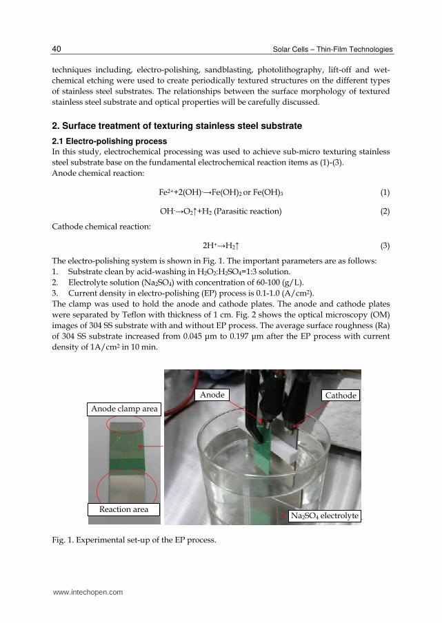
In this study, electrochemical processing was used to achieve sub-micro texturing stainless
steel substrate base on the fundamental electrochemical reaction items as (1)-(3).
Anode chemical reaction:
Fe2++2(OH)-}Fe(OH)2 or Fe(OH)3 (1)
OH-}O2|+H2 (Parasitic reaction) (2)
Cathode chemical reaction:
2H+}H2| (3)
The electro-polishing system is shown in Fig. 1. The important parameters are as follows:
1. Substrate clean by acid-washing in H2O2:H2SO4=1:3 solution.
2. Electrolyte solution (Na2SO4) with concentration of 60-100 (g/L).
3. Current density in electro-polishing (EP) process is 0.1-1.0 (A/cm2).
The clamp was used to hold the anode and cathode plates. The anode and cathode plates
were separated by Teflon with thickness of 1 cm. Fig. 2 shows the optical microscopy (OM)
images of 304 SS substrate with and without EP process. The average surface roughness (Ra)
of 304 SS substrate increased from 0.045 μm to 0.197 μm after the EP process with current
density of 1A/cm2 in 10 min.
陽極 陰極
Na2SO4電解液
Fig. 1. Experimental set-up of the EP process.
Cathode Anode
Na2SO4 electrolyte
Anode clamp area
Reaction area
www.intechopen.com

Enhanced Diffuse Reflection of Light by Using a Periodically Textured Stainless Steel Substrate
41
2.2 Sand blasting process The glass sand (#320) was used to form randomly textured surface with cave size of several μm to tens μm on the surface of stainless steel substrate. The average surface roughness (Ra) of 304 SS substrate increased from 0.277 μm to 6.535 μm after the sand blasting process. The OM images of raw 304 SS substrate and with sand blasting process were shown in Fig. 3.
Fig. 2. The OM images (x2000) of (a) raw 304 SS substrate surface and (b) 304 SS substrate surface with EP process.
Fig. 3. The OM images (x400) of (a) raw 304 SS substrate surface and (b) 304 SS substrate surface with sand blasting process.
2.3 Photolithography process The photo-mask patterns were designed by CAD. Photolithography is a process of using light to transfer a geometric pattern from a photo-mask to a photo-resist on a 430BA SS substrate. The steps involved in the photolithographic process are metal cleaning, barrier layer formation, photo-resist application, soft baking, mask alignment, exposure and development, and hard-baking. After the photolithographic process, the 430BA SS substrate is etched by aqua regia (HNO3 : HCl=1 : 3). There are two types of photo-mask patterns: one, different diameters but with the same interval, and two, the same diameters but with a different interval. They are both designed to study light trapping for the application of thin film solar cells. Finally, silver coating technique by e-beam evaporation was used to improve the TR and DR rates of the 430BA SS substrate.
(a) (b)
(a) (b)
www.intechopen.com

Solar Cells – Thin-Film Technologies
42
2.4 Lift-off and etching process In this study, lift-off and etching processes were used to fabricate the different textures of
the 304BA SS substrates. The striped texture was created on the 304BA SS substrate using
the lift-off process. After the hard-baking process, a silver (Ag) thin film was deposited on
the substrate by e-beam evaporation. An acetone solution was used to remove the residual
photo resistor (PR). The depth of the striped texture was controlled by the thickness of the
Ag thin film deposited. Four different striped textures were created on the 304BA SS
substrates, including period/height: 6/0.1, 6/0.3, 12/0.1 and 12/0.3 μm. Two other types of
textured 304BA SS substrate, the ridged-stripe and pyramid texture with 22.5 μm width
were created by the etching process. After hard-baking, the 304BA SS substrate was etched
by aqua regia (HNO3 : HCl : DI water=1 : 3 : 4). The etching temperature was 28-35℃ with
an etching time of 7-12 min. to control the etching depth of the textured 304BA SS substrate.
The detail experimental flow charts of lift-off and etching processes are shown in Fig. 4 and
Fig. 5, respectively.
3. Optical properties of textured stainless steel substrate
3.1 Measurements of optical properties of textured stainless steel substrate
The total reflection (TR) and diffuse reflection (DR) rates of incident light from the textured
substrate were carefully studied by using a Perkin Elmer Lambda 750S spectrometer. It was
known that the specula reflection takes place on a smooth surface, and the angle of reflection is
the same as the angle of incidence. DR is a phenomenon where an incident beam of light
strikes an uneven or granular surface and then scatters in all directions. In Fig. 6, the 6 cm
Fig. 4. The experimental flow charts of lift-off process.
1. Substrate cleaning
2. Coating PR
3. Softbake & exposing
UV light
mask
4. Development
Ag film
5. Hardbake & metal deposition
6. Removing PR
7. Metal deposition
AZ4620
Aceton
Developer SS 304BA
Ag film
www.intechopen.com

Enhanced Diffuse Reflection of Light by Using a Periodically Textured Stainless Steel Substrate
43
Integrating Sphere is used for diffuse reflectance measurements. Reflectance measurements include total and diffuse reflectance at an incident angle of 8 degrees. Specular reflectance can be calculated from the total and diffuse reflectance measurements. The TR and DR rate of a textured substrate are important indexes when increasing the light trapping efficiency of thin-films solar cells.
Fig. 5. The experimental flow charts of etching process.
Fig. 6. The total reflection and diffuse reflection measured by integrating Sphere.
www.intechopen.com

Solar Cells – Thin-Film Technologies
44
3.2 Optical properties on periodically textured 430BA stainless steel substrate Lately the light trapping properties of textured substrates have attracted substantial interest because of their potential to reduce the thickness of solar cell material. In this study, the different kinds of textured patterns formed on 430BA SS substrate have been proposed for the purpose of trapping light in the application of thin film solar cells. Figure 7 shows the surface morphology of the 430BA SS substrate etched by using aqua regia. It should be noted that the dark and light regions of the OM images indicate the concave structure and the flat surface on the textured 430BA SS substrate, respectively. In order to understand the optical reflection of a textured 430BA SS substrate, the Perkin Elmer Lambda 900 spectrometer was used to analyze both the TR and DR rates of incident light. The TR and DR rates versus the wavelength curves for the raw and textured 430BA SS substrates are shown in Fig. 8 and Fig. 9, respectively. The “D” and “G” indicate the diameter and the gap for these periodically textured 430BA SS substrates, respectively. It must be noted that the discontinued data line in the wavelength of 850 to 950nm was due to the change in detector, from a PMT to a PbS detector. First, we compared the textured 430BA SS substrates with different diameters of 2, 4 and 6μm and with the same interval of 3μm. In Fig. 8, it was found that the DR rate at the wavelength of 600nm increases substantially, from 4.5% of a raw 430BA SS substrate to 19.7 %, 23.1% and 31.8% for textured 430BA SS substrates with a diameter of 2, 4 and 6μm, respectively. It was evident that for the same areas of analysis, the larger the size of the concave shape, the worse the TR rate would
Fig. 7. The OM images of a concave periodically textured 430BA SS substrate with a diameter/gap of (a) 4/5 μm (b) 4/7 μm (c) 4/3 μm (d) 6/3 μm.
200 400 600 800 1000 1200
30
40
50
60
70
80
90(a)
Tota
l re
flection r
ate
(%
)
Wavelength (nm)
430BA D4G3
D2G3 D6G3
200 400 600 800 1000 12000
10
20
30
40
50
60(b)
Diffu
se r
eflection r
ate
(%
)
Wavelength (nm)
430BA D4G3
D2G3 D6G3
Fig. 8. The TR and DR rates versus the wavelength curves for raw 430BA SS substrate at different diameter of textured 430BA SS substrate.
(a) (b) (c) (d)
www.intechopen.com
Enhanced Diffuse Reflection of Light by Using a Periodically Textured Stainless Steel Substrate
45
200 400 600 800 1000 1200
30
40
50
60
70
80
90(a)
Tota
l re
flection r
ate
(%
)
Wavelength (nm)
430BA D4G5
D4G3 D4G7
200 400 600 800 1000 12000
10
20
30
40
50(b)
Diffu
se r
eflection r
ate
(%
)
Wavelength (nm)
430BA D4G5
D4G3 D4G7
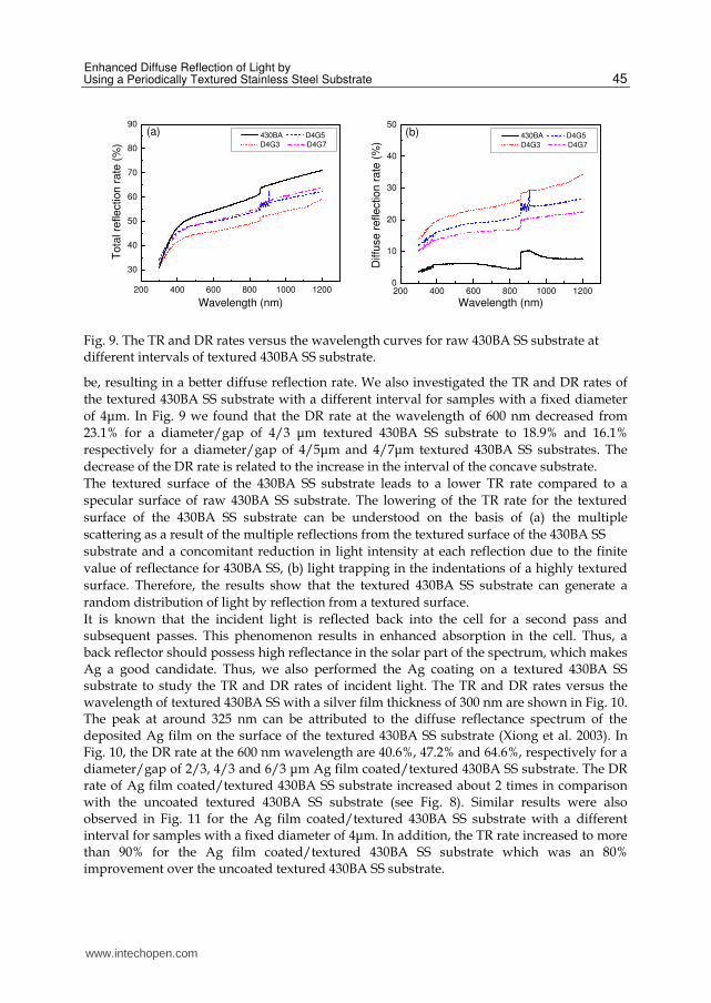
Fig. 9. The TR and DR rates versus the wavelength curves for raw 430BA SS substrate at different intervals of textured 430BA SS substrate.
be, resulting in a better diffuse reflection rate. We also investigated the TR and DR rates of
the textured 430BA SS substrate with a different interval for samples with a fixed diameter
of 4μm. In Fig. 9 we found that the DR rate at the wavelength of 600 nm decreased from
23.1% for a diameter/gap of 4/3 μm textured 430BA SS substrate to 18.9% and 16.1%
respectively for a diameter/gap of 4/5μm and 4/7μm textured 430BA SS substrates. The
decrease of the DR rate is related to the increase in the interval of the concave substrate.
The textured surface of the 430BA SS substrate leads to a lower TR rate compared to a
specular surface of raw 430BA SS substrate. The lowering of the TR rate for the textured
surface of the 430BA SS substrate can be understood on the basis of (a) the multiple
scattering as a result of the multiple reflections from the textured surface of the 430BA SS
substrate and a concomitant reduction in light intensity at each reflection due to the finite
value of reflectance for 430BA SS, (b) light trapping in the indentations of a highly textured
surface. Therefore, the results show that the textured 430BA SS substrate can generate a
random distribution of light by reflection from a textured surface.
It is known that the incident light is reflected back into the cell for a second pass and subsequent passes. This phenomenon results in enhanced absorption in the cell. Thus, a back reflector should possess high reflectance in the solar part of the spectrum, which makes Ag a good candidate. Thus, we also performed the Ag coating on a textured 430BA SS substrate to study the TR and DR rates of incident light. The TR and DR rates versus the wavelength of textured 430BA SS with a silver film thickness of 300 nm are shown in Fig. 10. The peak at around 325 nm can be attributed to the diffuse reflectance spectrum of the deposited Ag film on the surface of the textured 430BA SS substrate (Xiong et al. 2003). In Fig. 10, the DR rate at the 600 nm wavelength are 40.6%, 47.2% and 64.6%, respectively for a diameter/gap of 2/3, 4/3 and 6/3 μm Ag film coated/textured 430BA SS substrate. The DR rate of Ag film coated/textured 430BA SS substrate increased about 2 times in comparison with the uncoated textured 430BA SS substrate (see Fig. 8). Similar results were also observed in Fig. 11 for the Ag film coated/textured 430BA SS substrate with a different interval for samples with a fixed diameter of 4μm. In addition, the TR rate increased to more than 90% for the Ag film coated/textured 430BA SS substrate which was an 80% improvement over the uncoated textured 430BA SS substrate.
www.intechopen.com

Solar Cells – Thin-Film Technologies
46
200 400 600 800 1000 120050
60
70
80
90
100(a)
Tota
l re
flection r
ate
(%
)
Wavelength (nm)
D2G3-Ag
D4G3-Ag
D6G3-Ag
200 400 600 800 1000 12000
10
20
30
40
50
60
70
80(b)
Diffu
se r
eflection r
ate
(%
)
Wavelength (nm)
D2G3-Ag
D4G3-Ag
D6G3-Ag
Fig. 10. The TR and DR rates versus wavelength curves for Ag film deposited at different diameter of textured 430BA SS substrate.
200 400 600 800 1000 12000
20
40
60
80
100(a)
Tota
l re
flection r
ate
(%
)
Wavelength (nm)
D4G3-Ag
D4G5-Ag
D4G7-Ag
200 400 600 800 1000 12000
10
20
30
40
50
60(b)
Diffu
se r
eflection r
ate
(%
)
Wavelength (nm)
D4G3-Ag
D4G5-Ag
D4G7-Ag
Fig. 11. The TR and DR rates versus wavelength curves for Ag film deposited at different intervals of textured 430BA SS substrate.
0 10 20 30 40 500
10
20
30
40
50
60
70
0
10
20
30
40
50
60
70
Tota
l refle
ctio
n ra
te (%
)
Diffu
se r
eflection r
ate
(%
)
Etch pit area/total surface area (%)
(a)
0 10 20 30 40 500
20
40
60
80
100
0
20
40
60
80
100(b)
Tota
l refle
ctio
n ra
te (%
)
Diffu
se r
eflection r
ate
(%
)
Etch pit area/total surface area (%)
Fig. 12. The TR and DR rates as a function of the ratio of the etch pit area to the total surface area for (a) the textured 430BA SS and (b) the Ag film coated/textured 430BA SS.
www.intechopen.com
Enhanced Diffuse Reflection of Light by Using a Periodically Textured Stainless Steel Substrate
47
From Fig. 8, it is evident that the TR and DR rates are not only dependent on the size of the concave shape but also depend on the interval of the concave substrate. Fig. 12(a) and (b) show the TR rate and DR rates as a function of the ratio of the etch pit area to the total surface area for the textured 430BA SS and the Ag film coated/textured 430BA SS, respectively. The ratio of the etch pit area to the total surface area is calculated by the number of pit in the total surface area multiplied by the single pit area divided by the total surface area. The total surface area is the analysis area in the spectrometer, measuring 1 cm2. It is evident that the DR rate increased with the increase effectiveness of the pit regions compared to the smooth regions for both the textured 430BA SS and the Ag film coated/textured 430BA SS. However, the TR rate showed the opposite trend compared with the DR rate and decreased with the increase of the ratio of the etch pit area to total surface area. It is worth noting that once again the TR rate for the the Ag film coated/textured 430BA SS was more than 90% even the ratio of the etch pit area to the total surface area was 50%. As shown in Figs. 8-11, we found that the increase in TR and DR rates as increase in light wavelength differed in the infrared range. The TR and DR rates clearly increased with the increasing light wavelength of the textured 430BA SS substrate. However, the TR and DR rates didn’t increase with the increasing light wavelength of the Ag film coated/textured 430BA SS substrate. Huang et al. indicated that a metal with a lower work function can enhance the Raman signal of diamond films, which is referred to as surface-enhanced Raman scattering (SERS) (Huangbr et al. 2000). A very similar effect, surface-enhanced infrared absorption (SEIRA) was reported to occur with thin metal films (Hartstein et al. 1980, Hatta et al. 1982, Osawa 1997). Moreover, it was reported that the enhancement depends greatly on the morphology of the metal surface (Nishikawa et al. 1993). Fig. 13 shows the SEM image of an Ag film coated/textured 430BA SS substrate. It was found that the surface was covered with Ag particles ranging in size from tens to hundreds of nanometers. Thus, we believe that the difference in increase of the TR and DR rates in the infrared range for the textured 430BA SS and the Ag film coated/textured 430BA SS reflectors are due to the absorption in the infrared range by the Ag films. Further, the surface morphology was related to the thickness of the Ag film and must be carefully investigated in future study.
Fig. 13. The SEM image of Ag film coated/textured 430BA SS substrate.
3.3 Optical properties on periodically textured 304BA stainless steel substrate Fig. 14 shows the OM images of the striped texture on the 304BA SS substrate. There are four patterns (i.e. the period/depth of 12/0.1, 12/0.3, 6/0.1, and 6/0.3 μm) which are designed and
www.intechopen.com

Solar Cells – Thin-Film Technologies
48
used to study the TR and DR rates of the 304BA SS substrate. The stripe width and depth of the samples were measured by a surface profiler. The TR and DR rates versus the wavelength curves for untreated and the stripe-textured 304BA SS substrates are shown in Fig. 15. The “P” and “D” indicate the period and the depth for the periodically textured 304BA SS substrates, respectively. It was found that the DR rate at the wavelength of 600 nm increased substantially, from 3.5% of an untreated 304BA SS substrate to 10.5%, 21.8%, 18.2% and 39.4% for textured 304BA SS substrates with a period/depth of 12/0.1, 12/0.3, 6/0.1, and 6/0.3 μm, respectively. In addition, the TR rate of the untreated 304BA SS was 67.7% and increased to ~97% for the striped textured 304BA SS substrate due to the high reflection of the Ag film on its surface. It was evident that for the same areas of analysis, the smaller the period and the larger the depth, the better the DR rate would be, resulting in a better diffuse reflection rate.
Fig. 14. The OM images of the stripe-textured 304BA SS substrate with a period/depth of (a) 12/0.1 μm (b) 12/0.3 μm (c) 6/0.1 μm (d) 6/0.3 μm.
400 450 500 550 600 650 70040
50
60
70
80
90
100 (a)
T
ota
l re
flection r
ate
(%
)
Wavelength (nm)
304BA P6H0.1 P12H0.1
P6H0.3 P12H0.3
400 450 500 550 600 650 7000
10
20
30
40
50(b)
Diffu
se r
eflection r
ate
(%
)
Wavelength (nm)
304BA P6H0.1 P12H0.1
P6H0.3 P12H0.3
Fig. 15. The TR and DR rates versus the wavelength curves for untreated and stripe-textured 304BA SS substrates.
(d)
(b)(a)
(c)
www.intechopen.com

Enhanced Diffuse Reflection of Light by Using a Periodically Textured Stainless Steel Substrate
49
In our previous study (Lee et al. 2009), it was found that for a textured 430BA SS substrate the DR rate increased with the increased effectiveness of the etch-pit regions compared to that of the smooth regions. Thus, the large and deeply etched areas of the textured 304BA SS indicated that they can improve the DR rate of a textured 304BA SS substrate. In order to improve the DR rate even further, we design two other kinds of textured 304BA SS substrates, the ridged-stripe and the pyramid texture. 3D images of the ridged-stripe and pyramid texture are shown in Figs. 16(a) and (b), respectively. The etching depth and the width for both textured 304BA SS substrates were estimated to be ~6.5 μm and ~22.5 μm, respectively. The aspect ratio (i.e. depth/width) was ~1/3.5 indicating that the opening
angle of the textured surface was about ~120o. It should be noted that the etching depth is controlled by the PR thickness and the etching time. In general, a thick PR and a long etching time can create the deeper textured 304BA SS substrate.
Fig. 16. The 3D images of (a) ridged-stripe and (b) pyramid 304BA SS substrate.
The TR and DR rates of the ridged-stripe and pyramid textured 304BA SS substrates are shown in Fig. 17. We found that the DR rate at the wavelength of 600 nm increased from 3.5 % for the untreated 304BA SS substrate to 60.1% for the pyramid and 63.1% for the ridged-stripe textured 304BA SS substrate. In addition, the DR rate also increased 1.5 times at the period/depth of 6/0.3 μm for the stripe-textured 304BA SS substrate. However, the textured substrates had a lower TR rate compared to the untreated 304BA SS substrate. The lowering of the TR rate for the textured surface of the 304BA SS substrate can be explained as follows (a) the multiple scattering is the result of the multiple reflections from the ridged-stripe or pyramid textured surface of the 304BA SS substrate, and the etching pit reduction in light intensity at each reflection is due to the finite value of the reflectance for the 304BA SS substrate, (b) light trapping occurs in the indentations of a highly textured surface. Therefore, the results show that the textured 304BA SS substrate can generate a random distribution of light through reflection from a textured surface. It is well known that the incident light is reflected back into the cell for a second pass and subsequent passes. This phenomenon results in enhanced absorption in the cell. Thus, a back reflector must possess high reflectance in the solar part of the spectrum, making Ag or Al good candidates. However, Al films absorb the incident light wavelength of 800 nm and reduce the light conversion efficiency. On the other hand, the reflection of Ag film can achieve 99% from the visible to the IR wavelength (Jenkins and white 1957). Thus, we also used an Ag coating on a textured 304BA SS substrate to study the TR and DR rates of incident light. The TR and DR rates versus the wavelength of ridged-stripe and pyramid textured 304BA SS substrates with a silver film thickness of 150 nm are shown in Fig. 18. The
(b) (a)
www.intechopen.com

Solar Cells – Thin-Film Technologies
50
DR rates at the 600 nm wavelength were 95.6% and 96.8%, for the ridged-stripe and pyramid Ag film coated/texture 304BA SS substrates, respectively. The DR rate increased about 15-fold in comparison with the Ag coated untreated 304BA SS substrate. In addition, the TR rates at the 600 nm wavelength were 96.7% and 96.8%, for the ridged-stripe and pyramidal Ag film coated/texture 304BA SS substrates, respectively.
400 450 500 550 600 650 700
55
60
65
70
75
(a)
Ridged-stripe
Pyramid
Tota
l re
flection r
ate
(%
)
Wavelength (nm)
400 450 500 550 600 650 70045
50
55
60
65
70(b)
Ridged-stripe
PyramidDiffu
se
re
fle
ction
ra
te (
%)
Wavelength (nm)
Fig. 17. The TR and DR rates versus the wavelength curves for ridged-stripe and pyramid textured 304BA SS substrates.
400 450 500 550 600 650 70050
60
70
80
90
100(a)
T
ota
l re
flection r
ate
(%
)
Wavelength (nm)
304BA
304BA/Ag
ridged-stripe/Ag
pyramid/Ag
400 450 500 550 600 650 7000
20
40
60
80
100(b)
Diffu
se r
eflection r
ate
(%
)
Wavelength (nm)
304BA
304BA/Ag
ridged-stripe/Ag
pyramid/Ag
Fig. 18. The TR and DR rates versus the wavelength curves for Ag films coated/untreated 304BA SS substrate and Ag film coated/ridged-stripe and pyramid textured 304BA SS substrates.
Fig. 19 shows the relationship between the DR/TR rates and the total effective area of the
Ag film coated/textured 304BA SS substrate. It should be noted that the total effective area
was defined by the incident light reaching the textured 304BA SS substrate in an area of
100×100 μm2. For example, the total effective area of the stripe textured 304BA SS substrate
was calculated by the etched side wall area added to the untreated area of 10000 μm2. For
the ridged-stripe textured 304BA SS, the total effective area was calculated by summing the
www.intechopen.com

Enhanced Diffuse Reflection of Light by Using a Periodically Textured Stainless Steel Substrate
51
nine ridged-surfaces within an area measuring 100×100 μm2. For the pyramid textured
304BA SS substrate, the total effective area was calculated by adding 25 pyramid-textured
surfaces to the no-pyramid-coverage areas. Since the high reflection property of Ag films,
the TR rate was almost higher than 90% after Ag-film coating of the textured 304BA SS
substrates. It is worth noting that the DR rate increased linearly with the increase in total
effective area of the stripe-textured 304BA SS substrate. However, the increase of the DR rate
with the increase in the total effective area for the ridged-stripe and pyramid textured 304BA
SS substrate was much more dramatic. We believe that the dramatic increase in the DR rate
was due to the fact that the textured surface generated a random distribution of light by
reflection from the textured surface. The aspect ratio for the ridged-stripe and pyramidal
textured 304BA SS substrate were about 1/3.5 with an opening angle of 120o. In addition, the
diffuse rate was defined when the incident light angle was zero, and the reflection light of that
angle was larger than 80 over the incident light. Thus, the increased light diffuse due to the
120o opening angle of the texture surface caused the dramatic increase of the DR rate for the
ridged-stripe and pyramid textured 304BA SS substrate. In addition, weakly absorbed light is
totally reflected internally at the top surface of the cell as long as the angle of incidence inside
the a-Si at the a-Si/TCO interface is greater than 160 (Banerjee and Guha 1991). It was indicated
that the tilt angle of the V-shaped light trapping configuration substantially increases the
photocurrent generation efficiency (Rim et al. 2007). The photocurrent increased with the
increase of the tilt angle of the V-shaped configuration and is believed to enhance the number
of ray bounces per unit cell area over that in a planar structure at each point in the V-fold
structure. Therefore, the tilted angle of the textured surface is related to the DR and TR rate,
and must be carefully investigated in future study.
9900 10200 10500 10800 11100 11400 117000
20
40
60
80
100
0
20
40
60
80
100
Tota
l refle
ctio
n ra
te (%
)D
iffu
se r
eflection r
ate
(%
)
Total effective area (m2)
Fig. 19. The TR and DR rates as a function of the total effective area for Ag films coated on textured 304BA SS substrates.
4. Conclusions
We have demonstrated that a large diameter or a small interval of a concave shaped
structure made from textured 430BA SS substrate can improve the DR rate of light.
www.intechopen.com
Solar Cells – Thin-Film Technologies
52
However, the textured surface of a 430BA SS substrate led to a lower TR rate compared to a
specular surface of raw 430BA SS substrate. This was due to the trapping of light in the
hollows of the highly textured surface. Moreover, coating the textured 430BA SS substrate
with an Ag film substantially improved not only the DR rate but also the TR rate of the
incident light. The slow increase of the TR and DR rates versus the wavelength in the IR
region of the Ag coated/textured 430BA SS substrates was due to the Ag absorption effect.
We believe that Ag coated/textured 430BA SS substrates can generate a random distribution
of light, increase the light trapping efficiency and be applied in thin films solar cells.
In addition, the DR and TR rate of the stripe, ridged-stripe and pyramid textured 304BA SS
substrate were investigated to determine the optimal surface for increasing their light
trapping efficiency. The DR rate increased with the increase in the total effective area of the
Ag film coated/stripe textured 304BA SS substrate. It is believed that the tilt angle of the
textured 304BA SS substrate increases the DR rate. The experimental results showed that the
DR rate and the TR rate of the Ag film coated/ ridged-stripe textured 304BA SS substrate
can achieve up to ~97% and 98% efficiency, respectively. The DR and TR rate of the Ag film
coated/ridged-stripe textured 304BA SS substrates increased 28-fold and 1.4-fold,
respectively, compared with the untreated 304BA SS substrate. The drastically increased DR
rate is due to not only the increase in total effective area, but also to the decrease in the
opening angle of the ridged textured substrate which generates a more random distribution
of light by scattering.
5. Acknowledgment
The authors gratefully acknowledge the financial support from the National Science Council of Taiwan, R.O.C. under Contract No. NSC-98-2112-M155-001-MY3 and NSC-99-2221-E-155-065.
6. References
Banerjee A. and S. Guha. (1991). Study of back reflectors for amorphous silicon alloy solar
cell application. J. Appl. Phys., Vol. 69, pp. 1030., ISSN: 1089-7550
Curtin Benjamin, Rana Biswas, and Vikram Dalal. (2009). Photonic crystal based back
reflectors for light management and enhanced absorption in amorphous silicon
solar cells. Appl. Phys. Lett. Vol. 95, pp. 231102., ISSN: 1077-3118
Chau Joseph Lik Hang, Ruei-Tang Chen, Gan-Lin Hwang, Ping-Yuan Tsai and Chien-Chu
Lin. (2010). Transparent solar cell window module. Sol. Energy Mater. Sol. Cells.,
Vol. 94, pp. 588., ISSN: 0927-0248.
Deckman H. W., C. R. Wronski, H. Wittzke, and E. Yablonovitch. (1983). Optically enhanced
amorphous silicon solar cells. Appl. Phys. Lett., Vol. 42, pp. 968., ISSN: 1077-3118.
Ferlanto A. S., G. M. Ferreira, J. M. Pearce, C. R. Wronski, R. W. Collins, X. Deng, and G.
Ganguly. (2002). Analytical model for the optical functions of amorphous
semiconductors from the near-infrared to ultraviolet: Applications in thin film
photovoltaics. J. Appl. Phys., Vol. 92, pp. 2424., ISSN: 1089-7550
www.intechopen.com
Enhanced Diffuse Reflection of Light by Using a Periodically Textured Stainless Steel Substrate
53
Fung Taddy Y. Y. and H. Yang. (2008). Study on thermal performance of semi-transparent
building-integrated photovoltaic glazings. Energy and Buildings., Vol. 40, pp. 341-
350., ISSN: 0378-7788.
Hartstein A., J. R. Kirtley, J. C. Tsang. (1980). Enhancement of the Infrared Absorption from
Molecular Monolayers with Thin Metal Overlayers. Phys. Rev. Lett., Vol. 45, pp. 201.
, ISSN: 1079-7114
Hatta A., T. Ohshima, W. Suëtaka. (1982). Observation of the enhanced infrared absorption
of p-nitrobenzoate on Ag island films with an ATR technique. J. Appl. Phys. A., Vol.
29, pp. 71., ISSN: 2158-3226
Huang B. R., K. H. Chen, W. Z. Ke. (2000). Surface-enhanced Raman analysis of diamond
films using different metals. Mater. Lett., Vol.42, pp. 162., ISSN:0167-577X
He Chun, Ya Xiong, Jian Chen, Changhong, Xihai Zhu. (2003). Photoelectrochemical
performance of Ag–TiO2/ITO film and photoelectrocatalytic activity towards the
oxidation of organic pollutants. J. Photochem. Photobiol. A., Vol. 57, pp. 71., ISSN:
1010-6030
Jenkins F. A. and H. E. White. (McGraw Hill, New York, 1957). Fundamentals of Optics., P.
522. ISBN: 0070-8534-60
John A. E. St., U. S. Patent No. 3 487 223
Llopis F. and I. Tobías. (2005). The role of rear surface in thin silicon solar cells. Sol. Energy
Mater. Sol. Cells., Vol. 87, pp. 481., ISSN: 0927-0248
Lee Shuo Jen, Shiow Long Chen, Cheng Wei Peng, Chih Yuan Lin, Wen Cheng Ke. (2009).
Enhanced diffuse reflection of light into the air using silver coating on periodically
textured 430BA stainless steel substrate. Mater. Chem. Phys., Vol. 118, pp. 219-222.,
ISSN: 0254-0584
Müller J., B. Rech, J. Springer and M. Vanecek (2004). TCO and light trapping in silicon thin
film solar cells. Sol. Energy. Vol. 77, pp. 917., ISSN: 0038-092X
Nishikawa Y., T. Nagasawa, K. Fujiwara, M. Osawa. (1993). Silver island films for surface-
enhanced infrared absorption spectroscopy: effect of island morphology on the
absorption enhancement. Vib. Spectrosc., Vol. 6, pp. 43., ISSN: 0924-2031
Otte K., L. Makhova, A. Braun, I. Konovalov. (2006). Flexible Cu(In,Ga)Se2 thin-film solar
cells for space application. Thin Solid Films., Vol. 511, pp. 613., ISSN: 0040-6090
Osawa M. (1997). Dynamic Processes in Electrochemical Reactions Studied by Surface-
Enhanced Infrared Absorption Spectroscopy (SEIRAS). Bull. Chem. Soc. Jpn., Vol. 70,
pp. 2861., ISSN: 0009-2673
Rech B., O. Kluth, T. Repmann, T. Roschek, J. Springer, J. Müller, F. Finger, H. Stiebig, and
H. Wagner. (2002). New materials and deposition techniques for highly efficient
silicon thin film solar cells. Sol. Energy Mater. Sol. Cells., Vol. 74, pp. 439., ISSN:
0927-0248
Rim Seung-Bum, Shanbin Zhao, Shawn R. Scully, Michael D. McGehee and Peter Peumans.
(2007). An effective light trapping configuration for thin-film solar cells. Appl. Phys.
Lett. Vol. 91, pp. 243501. ISSN: 1077-3118
Selvan J. A. Anna., A. E. Delahoy, S. Guo and Y. M. Li. (2006). A new light trapping TCO for
nc-Si:H solar cells. Sol. Energy Mater. Sol. Cells., Vol. 90, pp. 3371., ISSN: 0927-0248
www.intechopen.com
Solar Cells – Thin-Film Technologies
54
Sőderstrőm T., F. –J. Haug, V. Terrazzoni-Daudrix, and C. Ballif, J. (2008). Optimization of
amorphous silicon thin film solar cells for flexible photovoltaics. J. Appl. Phys., Vol.
103, pp. 114509-1., ISSN: 1089-7550
Yablonovitch E. and G. Cody. (1982). Intensity enhancement in textured optical sheets for
solar cells. IEEE Trans. Electron. Devices ED., Vol. 29, pp. 300., ISSN: 0018-9383
Zhou Dayu and Rana Biswas. (2008). Photonic crystal enhanced light-trapping in thin film
solar cells. J. Appl. Phys., Vol. 103, pp. 093102. , ISSN: 1089-7550
www.intechopen.com

Solar Cells - Thin-Film TechnologiesEdited by Prof. Leonid A. Kosyachenko
ISBN 978-953-307-570-9Hard cover, 456 pagesPublisher InTechPublished online 02, November, 2011Published in print edition November, 2011
InTech EuropeUniversity Campus STeP Ri Slavka Krautzeka 83/A 51000 Rijeka, Croatia Phone: +385 (51) 770 447 Fax: +385 (51) 686 166www.intechopen.com
InTech ChinaUnit 405, Office Block, Hotel Equatorial Shanghai No.65, Yan An Road (West), Shanghai, 200040, China
Phone: +86-21-62489820 Fax: +86-21-62489821
The first book of this four-volume edition is dedicated to one of the most promising areas of photovoltaics,which has already reached a large-scale production of the second-generation thin-film solar modules and hasresulted in building the powerful solar plants in several countries around the world. Thin-film technologiesusing direct-gap semiconductors such as CIGS and CdTe offer the lowest manufacturing costs and arebecoming more prevalent in the industry allowing to improve manufacturability of the production at significantlylarger scales than for wafer or ribbon Si modules. It is only a matter of time before thin films like CIGS andCdTe will replace wafer-based silicon solar cells as the dominant photovoltaic technology. Photoelectricefficiency of thin-film solar modules is still far from the theoretical limit. The scientific and technologicalproblems of increasing this key parameter of the solar cell are discussed in several chapters of this volume.
How to referenceIn order to correctly reference this scholarly work, feel free to copy and paste the following:
Shuo-Jen Lee and Wen-Cheng Ke (2011). Enhanced Diffuse Reflection of Light by Using a PeriodicallyTextured Stainless Steel Substrate, Solar Cells - Thin-Film Technologies, Prof. Leonid A. Kosyachenko (Ed.),ISBN: 978-953-307-570-9, InTech, Available from: http://www.intechopen.com/books/solar-cells-thin-film-technologies/enhanced-diffuse-reflection-of-light-by-using-a-periodically-textured-stainless-steel-substrate

© 2011 The Author(s). Licensee IntechOpen. This is an open access articledistributed under the terms of the Creative Commons Attribution 3.0License, which permits unrestricted use, distribution, and reproduction inany medium, provided the original work is properly cited.