Embed Size (px)
Citation preview
Epitaxial Deposition
Daniel Lentz
EE 518Penn State University
March 29, 2007Instructor: Dr. J. Ruzyllo
Outline
IntroductionMechanism of epitaxial growthMethods of epitaxial depositionProperties of epitaxial layersApplications of epitaxial layers
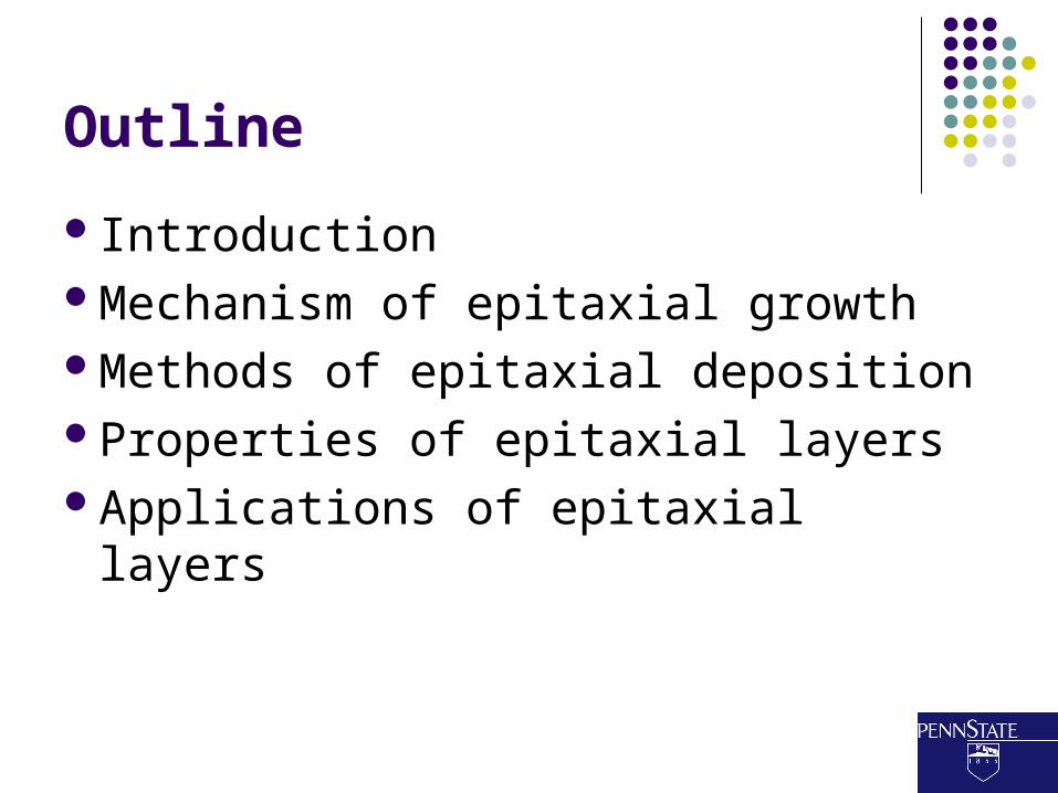
Epitaxial Growth Deposition of a layer on a
substrate which matches the crystalline order of the substrate
Homoepitaxy Growth of a layer of the
same material as the substrate
Si on Si Heteroepitaxy
Growth of a layer of a different material than the substrate
GaAs on Si
Ordered, crystalline growth; NOT epitaxial
Epitaxial growth:
Motivation
Epitaxial growth is useful for applications that place stringent demands on a deposited layer: High purity Low defect density Abrupt interfaces Controlled doping profiles High repeatability and uniformity Safe, efficient operation
Can create clean, fresh surface for device fabrication
General Epitaxial Deposition Requirements Surface preparation
Clean surface needed Defects of surface duplicated in epitaxial layer Hydrogen passivation of surface with water/HF
Surface mobility High temperature required heated substrate Epitaxial temperature exists, above which deposition is
ordered Species need to be able to move into correct
crystallographic location Relatively slow growth rates result
Ex. ~0.4 to 4 nm/min., SiGe on Si
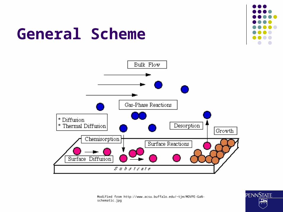
General Scheme
Modified from http://www.acsu.buffalo.edu/~tjm/MOVPE-GaN-schematic.jpg
Thermodynamics Specific thermodynamics varies by process
Chemical potentials Driving force
High temperature process is mass transport controlled, not very sensitive to temperature changes
Steady state Close enough to equilibrium that chemical forces that drive growth
are minimized to avoid creation of defects and allow for correct ordering
Sufficient energy and time for adsorbed species to reach their lowest energy state, duplicating the crystal lattice structure
Thermodynamic calculations allow the determination of solid composition based on growth temperature and source composition
Kinetics
Growth rate controlled by kinetic considerations Mass transport of reactants to surface Reactions in liquid or gas Reactions at surface Physical processes on surface
Nature and motion of step growth Controlling factor in ordering
Specific reactions depend greatly on method employed
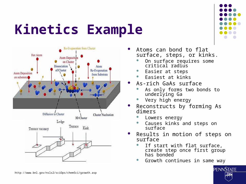
Kinetics Example Atoms can bond to flat surface,
steps, or kinks. On surface requires some critical
radius Easier at steps Easiest at kinks
As-rich GaAs surface As only forms two bonds to
underlying Ga Very high energy
Reconstructs by forming As dimers Lowers energy Causes kinks and steps on surface
Results in motion of steps on surface If start with flat surface, create step
once first group has bonded Growth continues in same way
http://www.bnl.gov/nsls2/sciOps/chemSci/growth.asp
Vapor Phase Epitaxy Specific form of chemical vapor deposition (CVD) Reactants introduced as gases Material to be deposited bound to ligands Ligands dissociate, allowing desired chemistry to
reach surface Some desorption, but most adsorbed atoms find
proper crystallographic position Example: Deposition of silicon
SiCl4 introduced with hydrogen Forms silicon and HCl gas Alternatively, SiHCl3, SiH2Cl2 SiH4 breaks via thermal decomposition
Precursors for VPE
Must be sufficiently volatile to allow acceptable growth rates
Heating to desired T must result in pyrolysis Less hazardous chemicals preferable
Arsine highly toxic; use t-butyl arsine instead VPE techniques distinguished by precursors
used
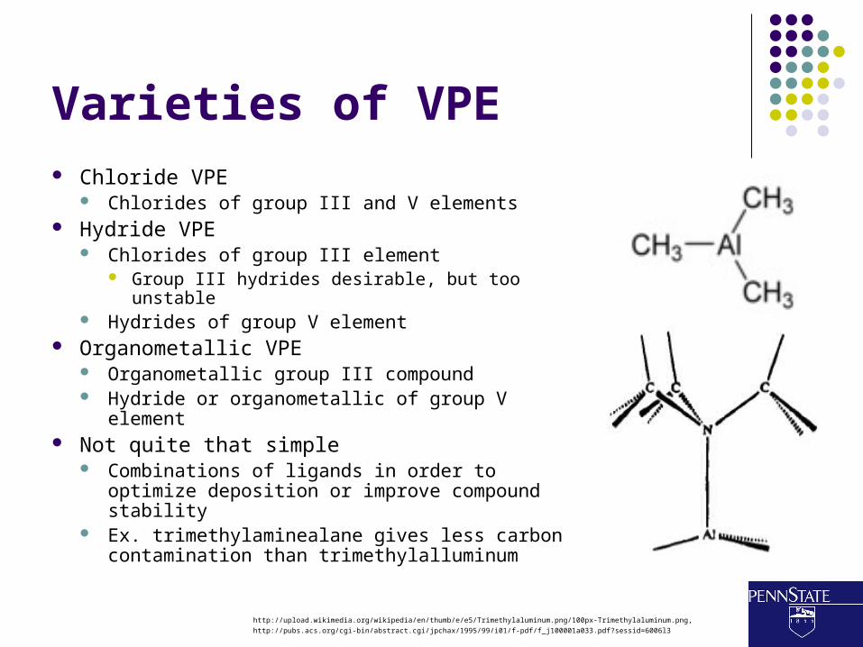
Varieties of VPE Chloride VPE
Chlorides of group III and V elements Hydride VPE
Chlorides of group III element Group III hydrides desirable, but too unstable
Hydrides of group V element Organometallic VPE
Organometallic group III compound Hydride or organometallic of group V element
Not quite that simple Combinations of ligands in order to optimize
deposition or improve compound stability Ex. trimethylaminealane gives less carbon
contamination than trimethylalluminum
http://upload.wikimedia.org/wikipedia/en/thumb/e/e5/Trimethylaluminum.png/100px-Trimethylaluminum.png,
http://pubs.acs.org/cgi-bin/abstract.cgi/jpchax/1995/99/i01/f-pdf/f_j100001a033.pdf?sessid=6006l3
Other Methods
Liquid Phase Epitaxy Reactants are dissolved in
a molten solvent at high temperature
Substrate dipped into solution while the temperature is held constant
Example: SiGe on Si Bismuth used as solvent Temperature held at
800°C High quality layer
Fast, inexpensive Not ideal for large area
layers or abrupt interfaces Thermodynamic driving
force relatively very low
Molecular Beam Epitaxy Very promising technique Elemental vapor phase
method Beams created by
evaporating solid source in UHV
Doping of Epitaxial Layers
Incorporate dopants during deposition Theoretically abrupt dopant distribution Add impurities to gas during deposition Arsine, phosphine, and diborane common
Low thermal budget results High T treatment results in diffusion of dopant into
substrate Reason abrupt distribution not perfect
Properties of Epitaxial Layer
Crystallographic structure of film reproduces that of substrate
Substrate defects reproduced in epi layer Electrical parameters of epi layer independent of
substrate Dopant concentration of substrate cannot be reduced Epitaxial layer with less dopant can be deposited
Epitaxial layer can be chemically purer than substrate
Abrupt interfaces with appropriate methods
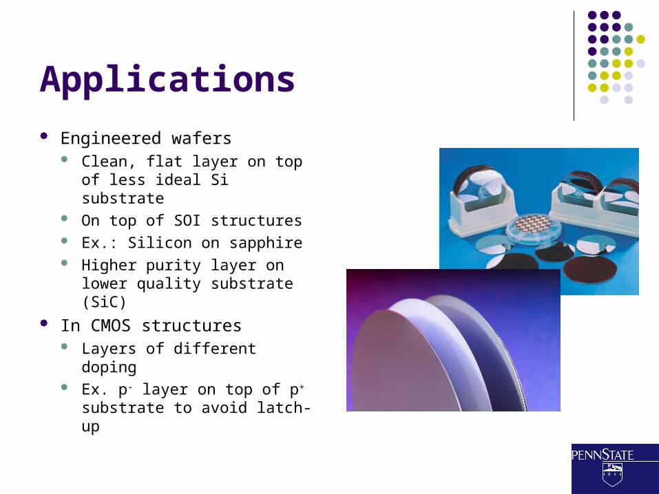
Applications
Engineered wafers Clean, flat layer on top of
less ideal Si substrate On top of SOI structures Ex.: Silicon on sapphire Higher purity layer on lower
quality substrate (SiC) In CMOS structures
Layers of different doping Ex. p- layer on top of p+
substrate to avoid latch-up
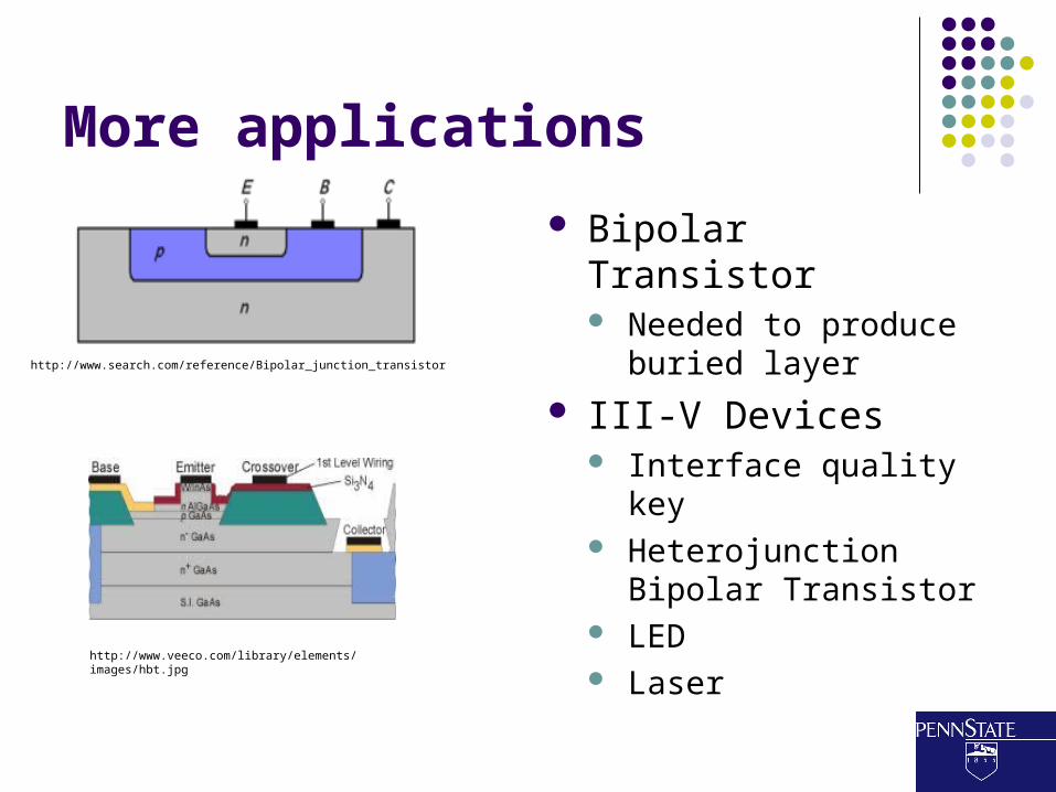
More applications
Bipolar Transistor Needed to produce
buried layer
III-V Devices Interface quality key Heterojunction Bipolar
Transistor LED Laser
http://www.veeco.com/library/elements/images/hbt.jpg
http://www.search.com/reference/Bipolar_junction_transistor
Summary
Deposition continues crystal structure Creates clean, abrupt interfaces and high
quality surfaces High temperature, clean surface required Vapor phase epitaxy a major method of
deposition Epitaxial layers used in highest quality wafers Very important in III-V semiconductor
production
References P. O. Hansson, J. H. Werner, L. Tapfer, L. P. Tilly, and E. Bauser, Journal of Applied
Physics, 68 (5), 2158-2163 (1990). G. B. Stringfellow, Journal of Crystal Growth, 115, 1-11 (1991). S. M. Gates, Journal of Physical Chemistry, 96, 10439-10443 (1992). C. Chatillon and J. Emery, Journal of Crystal Growth, 129, 312-320 (1993). M. A. Herman, Thin Solid Films, 267, 1-14 (1995). D. L. Harame et al, IEEE Transactions on Electron Devices, 42 (3), 455-468 (1995). G. H. Gilmer, H. Huang, and C. Roland, Computational Materials Science, 12, 354-380
(1998). B. Ferrand, B. Chambaz, and M. Couchaud, Optical Materials, 11, 101-114 (1999). R. C. Cammarata, K. Sieradzki, and F. Spaepen, Journal of Applied Physics, 87 (3),
1227-1234 (2000). R. C. Jaeger, Introduction to Microelectronic Fabrication, 141-148 (2002). R. C. Cammarata and K. Sieradzki, Journal of Applied Mechanics, 69, 415-418 (2002). A. N. Larsen, Materials Science in Semiconductor Processing, 9, 454-459 (2006).