Embed Size (px)
Citation preview
http://www.diva-portal.org
Postprint
This is the accepted version of a paper presented at Symposium on SiGe, Ge, and RelatedMaterials: Materials, Processing, and Devices 7 - PRiME 2016/230th ECS Meeting, 2October 2016 through 7 October 2016.
Citation for the original published paper:
Abedin, A., Asadollahi, A., Garidis, K., Hellström, P-E., Östling, M. (2016)Epitaxial growth of Ge strain relaxed buffer on Si with low threading dislocationdensity.In: ECS Transactions (pp. 615-621). Electrochemical Societyhttps://doi.org/10.1149/07508.0615ecst
N.B. When citing this work, cite the original published paper.
Permanent link to this version:http://urn.kb.se/resolve?urn=urn:nbn:se:kth:diva-201995

Epitaxial Growth of Ge Strain Relaxed Buffer on Si with
Low Threading Dislocation Density
A. Abedin, A. Asadollahi, K. Garidis, P.-E. Hellström and M. Östling
KTH Royal Institute of Technology, School of Information and Communication
technology, Electrum 229, 164 40 Kista, Sweden
Epitaxial Ge with low dislocation density is grown on a low
temperature grown Ge seed layer on Si substrate by reduced
pressure chemical vapor deposition. The surface topography
measured by AFM shows that the strain relaxation occurred
through pit formation which resulted in freezing the defects at
Ge/Si interface. Moreover a lower threading dislocation density
compared to conventional strain relaxed Ge buffers on Si was
observed. We show that by growing the first layer at temperatures
below 300 °C a surface roughness below 1 nm can be achieved
together with carrier mobility enhancement. The different defects
densities revealed from SECCO and Iodine etching shows that the
defects types have been changed and SECCO is not always
trustable.
Introduction
Germanium, with its superior electron and hole mobility compared to Si, is considered as
a channel material in future CMOS technology [1]. The bandgap of Ge (0.67 eV) also
makes it attractive in optoelectronic device applications working in the wavelength range
of 1.3-1.5 µm. However, integration of crystalline Ge on Si wafers is challenging due to
the high lattice mismatch (4.2%), which may cause two issues: misfit and threading
dislocations in Ge strain relaxed buffers (SRBs) and high surface roughness as a result of
Stransky-Krostanov growth [2]. Threading dislocations reaching the device layer can
degrade the carrier mobility and increase the junction leakage current of MOSFETs and
photodetectors. Several groups have reported that threading dislocation density (TDD)
can be reduced by different methods such as using compositionally graded SiGe buffer
layer [3], surfactant-mediated epitaxy [4], implementing a two-step growth and post
growth thermal anneal and/or cyclic thermal annealing [5]. The lowest TDDs of 106 cm
-2
has been achieved by selective epitaxy and using compositionally graded buffer [1].
However, selective epitaxy is a complex technique and compositionally graded buffers
need to be around 10 µm thick to achieve such low TDD.
In the two-step growth method, a thin strain relaxed Ge seed layer is grown on Si
substrate at a low temperature to suppress three dimensional islands growth. The growth
continues at high temperature with high quality Ge layer grown on the Ge template layer
[6]. The surface of the Ge layers grown with this method is smooth with surface
roughness around 2 nm. However, the TDDs of as grown layers are found to be
tremendously high, close to 109 cm
-2 and thermal annealing is required to lower the
defect density. Reports show that the TDD of 1 µm Ge layer with ten times cyclic
thermal annealing at 780 °C /900 °C can be reduced to 2·107 cm
-2 [1] and increasing the
thickness of the layer to more than 2µm can even reduce the TDD to 6·106 cm
-2 [7].
10.1149/07508.0615ecst ©The Electrochemical SocietyECS Transactions, 75 (8) 615-621 (2016)
615) unless CC License in place (see abstract). ecsdl.org/site/terms_use address. Redistribution subject to ECS terms of use (see 130.237.37.119Downloaded on 2017-09-10 to IP

However, the thermal annealing is not always applicable since it causes dopants out
diffusion and also Si and Ge atoms intermixing at their interface.
However, a thin Ge film with smooth surface and low TDD is still not achieved. In this
work, we show further reduction of the Ge growth temperature (and optimization of its
profile) during the initial step to less than 300 °C together with using Ge2H6 as precursor
enables a 0.5 µm thin Ge SRB with surface roughness below 1 nm, TDDs as low as 5·108
cm-2
and room temperature carrier mobility of 950 cm2.V
-1.s
-1 directly on silicon.
Experiments
The Ge SRB was grown on (100) oriented 100 mm Si wafers by reduced pressure (20
torr) chemical vapor deposition (RPCVD, ASM Epsilon 2000). Digermane (10% Ge2H6
in hydrogen) was used as Ge precursor and constant 20 standard liters per minute purified
H2 as the carrier gas. Phosphine (PH3 5% in hydrogen) and diborane (B2H6 10% in
hydrogen) were used as phosphorous and boron sources for n- and p-type Ge SRB growth,
respectively. The substrates were subjected to a RCA (H2SO4(96%):H2O2(30%) 3:1)
cleaning and dipped in HF (5% in DI water) before loading into the RPCVD reactor.
In-situ hydrogen bake was performed at T=1050 °C for 2 min to remove any residual
native oxide from the surface. The temperature was ramped down to 280 °C before the
Ge2H6 was introduced in the chamber followed by a temperature ramp up to 300 °C for
20 min growing a 40 nm strained relaxed Ge layer. The temperature was ramped up to
680 °C in H2 and a 460 nm thick Ge layer was grown at this temperature. For comparison,
a 3 µm thick Ge SRB was deposited with the conventional two step method; i.e. first
layer grown at T=400 °C followed by the second layer at T=680 °C and post growth
annealing at T=900 °C.
The topography and surface roughness of the grown layers were measured by AFM in
tapping mode. The crystal quality of the epitaxial layers was investigated with high
resolution X-Ray diffraction (HRXRD) rocking curve and high resolution reciprocal
lattice mapping (HRRLM) pattern. A Philips X’pert PANalytical diffractometer tool was
used for XRD measurements equipped with a copper anticathode and a four bounce
symmetric Ge monochromator. High resolution cross sectional transmission electron
microscopy (XTEM) measurement was performed to image the defects at the interface of
Ge and Si. The grown Ge SRB was subjected to wet chemical etching using SECCO
(K2Cr2O7:H2O:HF) and Iodine (HF:HNO3:CH3COOH:I) solutions in order to delineate
the threading dislocations. TDD was determined by counting delineated defects on
images obtained from both dark field optical microscope, AFM and SEM. Ge layers were
in situ doped with boron and phosphorous with dopant concentrations of 1017
cm-3
.
Wafers were diced to square pieces and four contacts were formed on each corner
through metallization and rapid thermal annealing at 300 °C for 90 sec. The carrier
mobility was extracted using four probe hall measurements. Both SIMS and four probe
sheet resistivity measurements were implemented to calculate the active dopant
concentrations.
ECS Transactions, 75 (8) 615-621 (2016)
616) unless CC License in place (see abstract). ecsdl.org/site/terms_use address. Redistribution subject to ECS terms of use (see 130.237.37.119Downloaded on 2017-09-10 to IP
Results and discussions
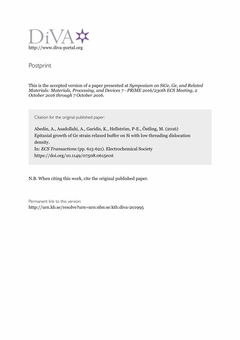
Fig. 1 shows AFM images of the surface morphology for temperature ramped
(T=280-300 °C) Ge SRB (left image) and conventional (T=400 °C) Ge SRB (right
image). The images indicate that the strain relaxation occurred through pit formation in
the temperature ramped Ge SRB while in the conventional Ge SRB, the strain relaxed
through island and valley formation. Similar relaxation through pit formation has been
reported in Ge grown on Si at T=290 °C using ultra high vacuum CVD and pure germane
as germanium source [8]. The pits are generated through stacking faults formations in
(111) planes and their dimensions depend on the thickness of the top layer. They are
formed in the first low temperature grown Ge layer below the brittle-ductile transition
temperature which allows Ge growth in 2D mode instead of 3D. The brittle-ductile
transition temperature depends on the experimental conditions and a sharp transition can
occur within a few degrees. it has been shown in [9] that the growth mode at
temperatures below the brittle-ductile transition results in strain relaxation through 90°
Lomer (edge) and screw dislocations formation instead of 60° dislocations . This type of
dislocations are sessile and cannot glide and thread into the next layer enabling low TDD
in the top Ge film grown at T=680 °C. The root mean squared (RMS) surface roughness
of the layers measured from tapping mode AFM images shows that the low temperature
growth has improved the surface quality of the grown layers from RMS ~ 2 nm to <1 nm
when temperature is decreased from 400 °C to lower than 300 °C which is in a good
agreement with the trend reported in [8].
Figure 1. AFM surface morphology of Ge SRB showing a) pit formation during strain
relaxation with the first layer grown at 280-300 °C and b) island and valley formation
when the first layer is grown at 400 °C.
HRXRD rocking curve of three different layers are shown in figure 2-a. The results
show when the layers have the same thickness, the layer grown at temperatures below
300 °C has smaller full width half maximum (FWHM) and higher peak intensity which
indicates its higher crystal quality. When the thickness is increased to 3 µm and the layer
is annealed, the Ge peak intensity has increased and the peak is broadened toward Si peak
which is due to Si and Ge atoms inter-diffusion at the interface. The HRRLM pattern
around [224] direction of the layers with the same thickness is shown in figure 2-b. The
results show less peak broadening for Ge SRB with the first layer grown at temperatures
a) b)
ECS Transactions, 75 (8) 615-621 (2016)
617) unless CC License in place (see abstract). ecsdl.org/site/terms_use address. Redistribution subject to ECS terms of use (see 130.237.37.119Downloaded on 2017-09-10 to IP

below 300 °C compare to the Ge SRB with the first layer grown at 400 °C. The peak
broadening indicates higher amount of imperfections.
32 33 34 35
101
102
103
104
105
106
GeSi
500nm Ge first layer at 400C
500nm Ge first layer at<300C
3µm Ge first layer at 400C + TA
Co
unts
Omega/2Theta (°)
Figure 2. a) XRD rocking curve of 500 nm Ge SRB with the first layer grown at 280-
300 °C, 500 nm Ge SRB with the first layer grown at 400 °C and 3 µm Ge SRB with the
first layer grown at 400 °C and thermally annealed at 820 °C for 20 min, b) HRRLM
pattern around the [224] direction of 500 nm Ge SRB with the first layer grown at 400 °C
(left image) and 500 nm Ge SRB with the first layer grown at 280-300 °C (right image).
SIMS results show that the layers have 1017
cm-3
atomic boron concentration.
Four-probe Hall measurement results show when the first layer is grown at temperatures
below 300 °C the hole Hall mobility at room temperature and 77 K are 950 and 1450
cm2.V
-1.s
-1, respectively which are very close to values of 1200 and 2000 cm
2.V
-1.s
-1 for
bulk p-type Ge. In case of conventional SRB layer, the Hall mobility values were 450 and
780 cm2.V
-1.s
-1 at room temperature and 77 K, respectively. The reason for such
significant carrier mobility reduction is the type and electrical activity of the dislocations
and the defects. The 60° dislocations which are the main defects of conventional Ge
a)
b)
ECS Transactions, 75 (8) 615-621 (2016)
618) unless CC License in place (see abstract). ecsdl.org/site/terms_use address. Redistribution subject to ECS terms of use (see 130.237.37.119Downloaded on 2017-09-10 to IP
buffers have a raw of broken dangling bonds in their core along their axis which is
believed to be the primary reason for electrical activity of dislocations. But the screw
dislocations have no broken dangling bonds, thereby, they are less electrically active and
do not increase the carrier scatterings [10].
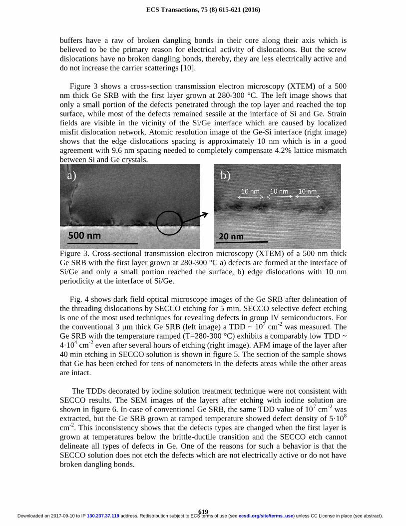
Figure 3 shows a cross-section transmission electron microscopy (XTEM) of a 500
nm thick Ge SRB with the first layer grown at 280-300 °C. The left image shows that
only a small portion of the defects penetrated through the top layer and reached the top
surface, while most of the defects remained sessile at the interface of Si and Ge. Strain
fields are visible in the vicinity of the Si/Ge interface which are caused by localized
misfit dislocation network. Atomic resolution image of the Ge-Si interface (right image)
shows that the edge dislocations spacing is approximately 10 nm which is in a good
agreement with 9.6 nm spacing needed to completely compensate 4.2% lattice mismatch
between Si and Ge crystals.
Figure 3. Cross-sectional transmission electron microscopy (XTEM) of a 500 nm thick
Ge SRB with the first layer grown at 280-300 °C a) defects are formed at the interface of
Si/Ge and only a small portion reached the surface, b) edge dislocations with 10 nm
periodicity at the interface of Si/Ge.
Fig. 4 shows dark field optical microscope images of the Ge SRB after delineation of
the threading dislocations by SECCO etching for 5 min. SECCO selective defect etching
is one of the most used techniques for revealing defects in group IV semiconductors. For
the conventional 3 µm thick Ge SRB (left image) a TDD ~ 107 cm
-2 was measured. The
Ge SRB with the temperature ramped (T=280-300 °C) exhibits a comparably low TDD ~
4·104 cm
-2 even after several hours of etching (right image). AFM image of the layer after
40 min etching in SECCO solution is shown in figure 5. The section of the sample shows
that Ge has been etched for tens of nanometers in the defects areas while the other areas
are intact.
The TDDs decorated by iodine solution treatment technique were not consistent with
SECCO results. The SEM images of the layers after etching with iodine solution are
shown in figure 6. In case of conventional Ge SRB, the same TDD value of 107 cm
-2 was
extracted, but the Ge SRB grown at ramped temperature showed defect density of 5·108
cm-2
. This inconsistency shows that the defects types are changed when the first layer is
grown at temperatures below the brittle-ductile transition and the SECCO etch cannot
delineate all types of defects in Ge. One of the reasons for such a behavior is that the
SECCO solution does not etch the defects which are not electrically active or do not have
broken dangling bonds.
a) b)
ECS Transactions, 75 (8) 615-621 (2016)
619) unless CC License in place (see abstract). ecsdl.org/site/terms_use address. Redistribution subject to ECS terms of use (see 130.237.37.119Downloaded on 2017-09-10 to IP

Figure 4. Dark field optical microscope images of the Ge SRB after delineation of the
threading dislocations by SECCO etching of a) Conventional Ge buffer and b) Ge SRB
with the first layer grown at temperatures below 300 °C.
Figure 5. AFM surface topography of the Ge SRB after delineation of the threading
dislocations by SECCO etching for 40 min.
Figure 6. SEM images of the Ge SRB after delineation of the threading dislocations by
Iodine etching of a) Conventional Ge buffer and b) Ge SRB with the first layer grown at
temperatures below 300 °C.
a) b)
a) b)
ECS Transactions, 75 (8) 615-621 (2016)
620) unless CC License in place (see abstract). ecsdl.org/site/terms_use address. Redistribution subject to ECS terms of use (see 130.237.37.119Downloaded on 2017-09-10 to IP
Conclusions
We have shown that by using Ge2H6 and optimizing a low temperature (280-300 °C)
profile of the initial Ge growth it is possible to grow a 0.5 µm thin Ge SRB on Si with
surface roughness below 1 nm, threading dislocation density of about 5·108 cm
-2 with
high carrier mobility without any post growth annealing. When the first layer is grown at
temperatures below 300 °C, the strain relaxation happens through pit formation with edge
and screw dislocations instead of 60° dislocations. These defects have less dangling
bonds and consequently, they are less electrically active compared to 60° dislocations.
Our experimental results show that the SECCO etch is not always a reliable method for
etching Ge defects and there are some types of defects which would not be delineated by
the SECCO treatment. It is recommended to use multiple defect selective etching to
reveal all types of defects in hetroepitaxial grown Ge layers.
Acknowledgments
This project was funded by Swedish Foundation for Strategic Research (SSF). Prof.
Mattias Hammar is acknowledged for fruitful discussions.
References
[1] H.-C. Luan, D.R. Lim, K.K. Lee, K.M. Chen, J.G. Sandland, K. Wada, et al., Appl. Phys. Lett. 75
(1999) 2909. doi:10.1063/1.125187.
[2] Y. Yamamoto, P. Zaumseil, T. Arguirov, M. Kittler, B. Tillack, Solid. State. Electron. 60 (2011) 2–
6. doi:10.1016/j.sse.2011.01.032.
[3] M.T. Currie, S.B. Samavedam, T.A. Langdo, C.W. Leitz, E.A. Fitzgerald, Appl. Phys. Lett. 72
(1998) 1718–1720. doi:10.1063/1.121162.
[4] T.F. Wietler, E. Bugiel, K.R. Hofmann, Appl. Phys. Lett. 87 (2005) 1–3. doi:10.1063/1.2120900.
[5] J.M. Hartmann, J.F. Damlencourt, Y. Bogumilowicz, P. Holliger, G. Rolland, T. Billon, J. Cryst.
Growth. 274 (2005) 90–99. doi:10.1016/j.jcrysgro.2004.10.042.
[6] S. Huang, C. Li, Z. Zhou, C. Chen, Y. Zheng, W. Huang, et al., Thin Solid Films. 520 (2012) 2307–
2310. doi:10.1016/j.tsf.2011.09.023.
[7] J.M. Hartmann, A. Abbadie, A.M. Papon, P. Holliger, G. Rolland, T. Billon, et al., J. Appl. Phys.
95 (2004) 5905–5913. doi:10.1063/1.1699524.
[8] B.W. Cheng, H.Y. Xue, D. Hu, G.Q. Han, Y.G. Zeng, A.Q. Bai, et al., 5th Int. Conf. Gr. IV
Photonics, GFP. (2008) 140–142. doi:10.1109/GROUP4.2008.4638124.
[9] M. Hammar, F.K. LeGoues, J. Tersoff, M.C. Reuter, R.M. Tromp, Surf. Sci. 349 (1996) 129–144.
doi:10.1016/0039-6028(95)01068-8.
[10] C. Claeys, E. Simoen, Extended Defects in Germanium Fundamental and Technological Aspects,
Springer, Belgium (2008).
ECS Transactions, 75 (8) 615-621 (2016)
621) unless CC License in place (see abstract). ecsdl.org/site/terms_use address. Redistribution subject to ECS terms of use (see 130.237.37.119Downloaded on 2017-09-10 to IP