Embed Size (px)
Citation preview

An 11-bit 45MS/s pipelined ADC with rapid calibration of DAC errors in a
multi-bit pipeline stageImran Ahmed, David A. Johns
University of Toronto
ESSCIRC 2007Session A3L-G1
University of TorontoDepartment of Electrical and Computer Engineering

2
Overview
• Motivations• State of the art• Approach of this work
– Rapid calibration of gain and DAC errors in 1st
pipeline stage– Design in 0.18µm CMOS
• Measurement results• Summary
3
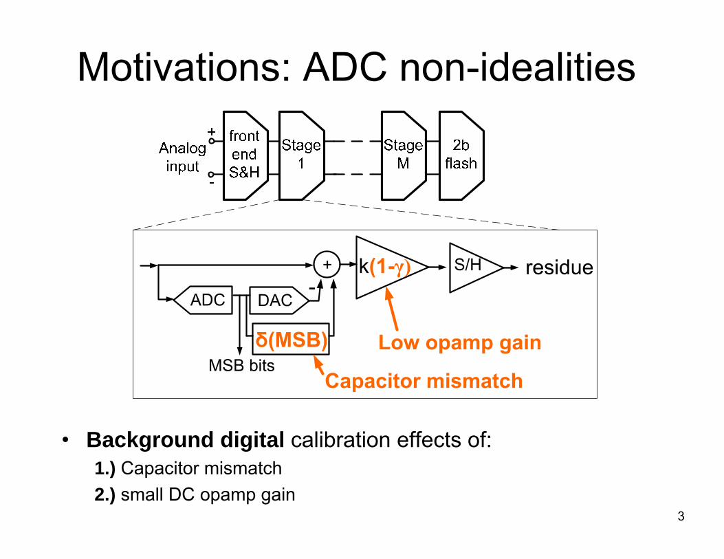
Motivations: ADC non-idealities
• Background digital calibration effects of:1.) Capacitor mismatch 2.) small DC opamp gain
4
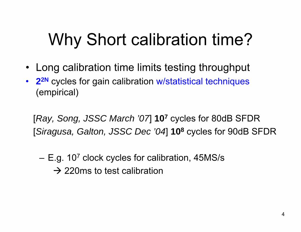
Why Short calibration time?• Long calibration time limits testing throughput• 22N cycles for gain calibration w/statistical techniques
(empirical)
[Ray, Song, JSSC March ’07] 107 cycles for 80dB SFDR[Siragusa, Galton, JSSC Dec ’04] 108 cycles for 90dB SFDR
– E.g. 107 clock cycles for calibration, 45MS/s 220ms to test calibration
5
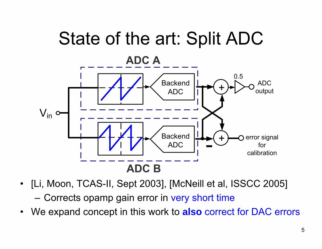
State of the art: Split ADC
• [Li, Moon, TCAS-II, Sept 2003], [McNeill et al, ISSCC 2005]– Corrects opamp gain error in very short time
• We expand concept in this work to also correct for DAC errors
in
BackendADC
BackendADC
ADC output
error signal for
calibration
0.5

6
4-bit pipeline stage residue: ideal
7
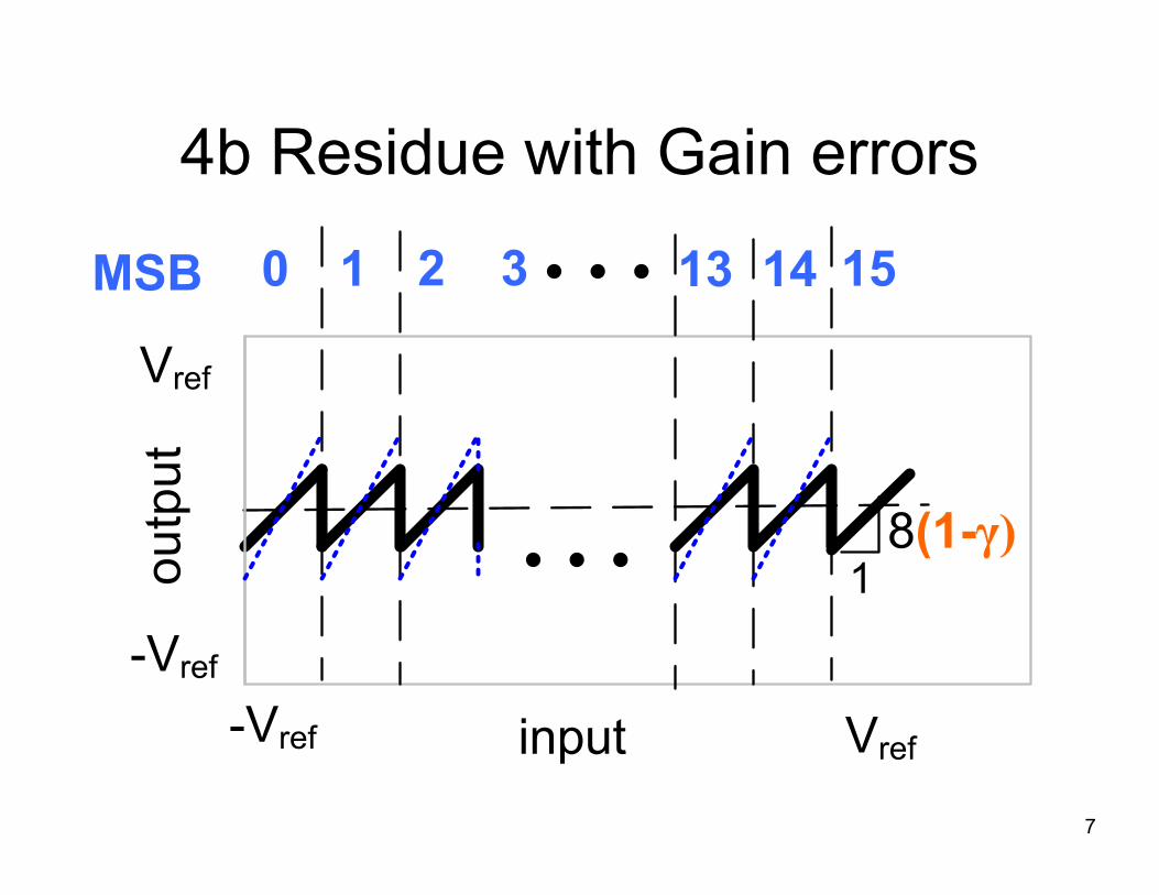
4b Residue with Gain errors
8
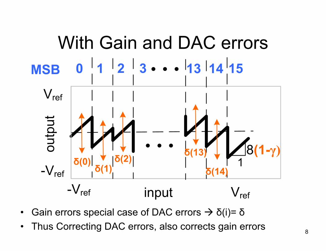
With Gain and DAC errors
• Gain errors special case of DAC errors δ(i)= δ• Thus Correcting DAC errors, also corrects gain errors
9
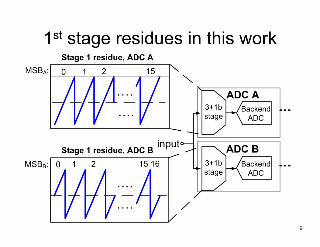
1st stage residues in this work
A
B

10
1st stage residues: no errors
MSBA
MSBB
LSBA(backend output)
LSBB(backend output)
Output of ADC A
Output of ADC B

11
1st stage residues: with DAC errors
• ADC A used as ideal reference to measure errors of ADC B• single DAC error measured with minimum of 2 clock cycles
MSBA
MSBB
LSBA(backend output)
LSBB(backend output)
error from missing codes
i2 i1

12
ADC A: error measurement
• Calibration requires input to be sufficiently busy to excite each MSB
A
B
A
B
i1 (i-1)2
13
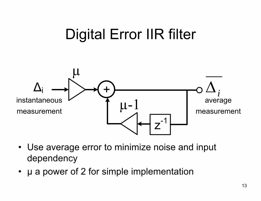
Digital Error IIR filter
• Use average error to minimize noise and input dependency
• µ a power of 2 for simple implementation
iΔ
14
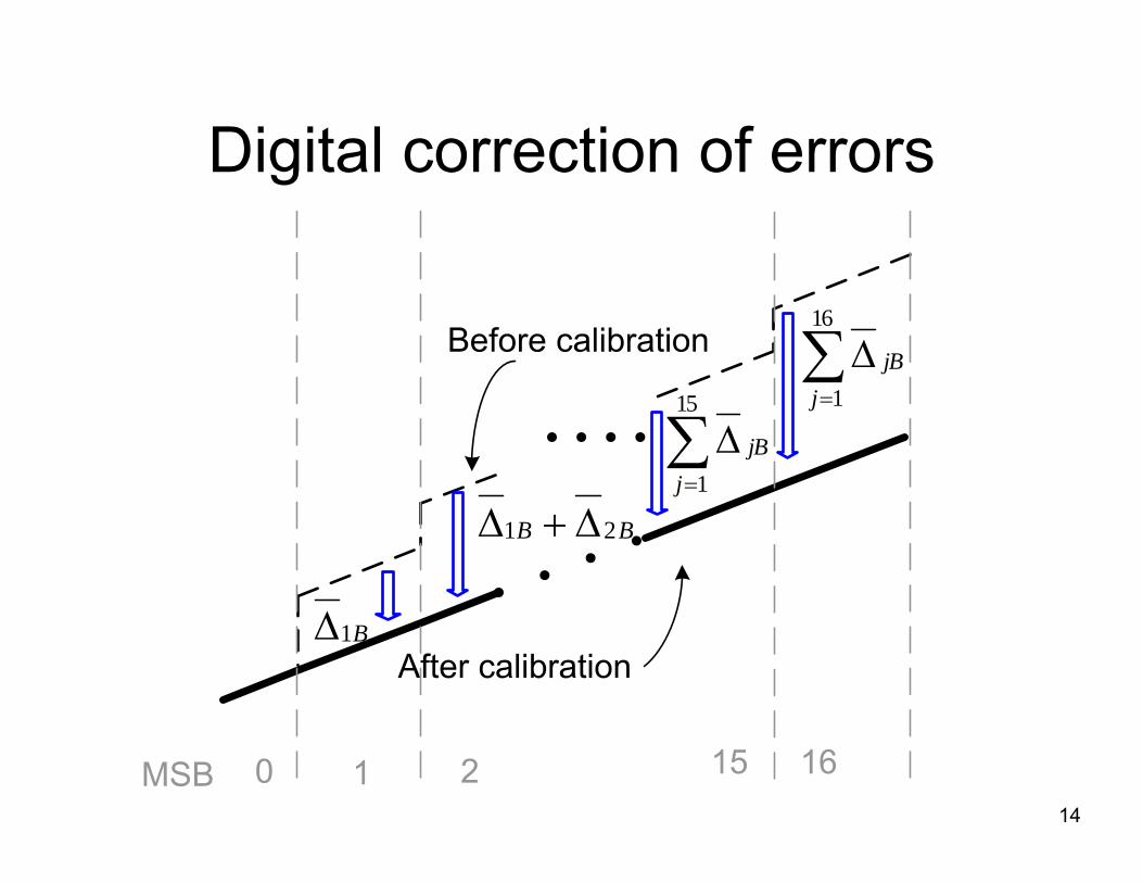
Digital correction of errors
∑=
Δ15
1jjB
B1Δ
BB 21 Δ+Δ
∑=
Δ16
1jjB
15
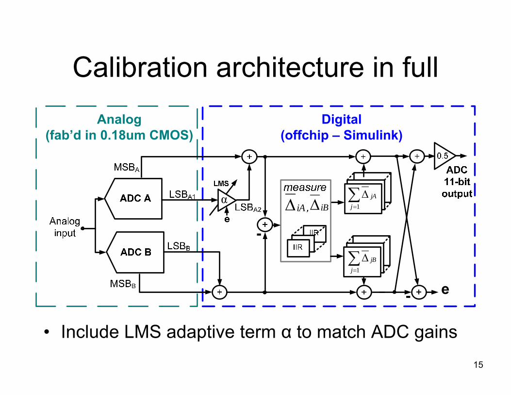
Calibration architecture in full
• Include LMS adaptive term α to match ADC gains
iAΔ iBΔ ∑=
Δ1j
jA
∑=
Δ1j
jB
16
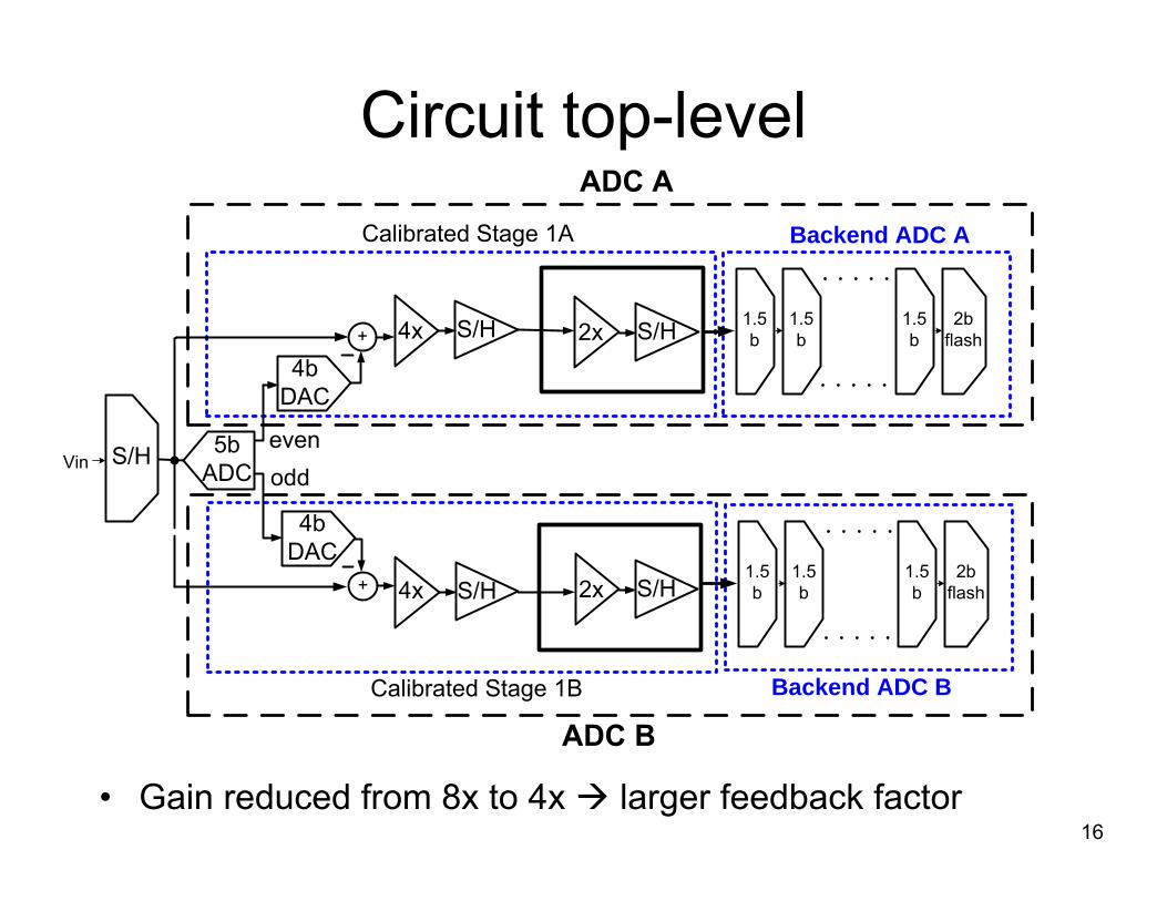
Circuit top-level
• Gain reduced from 8x to 4x larger feedback factor
S/HVin
4b DAC
+ 4x
5bADC
4b DAC
+ 4x
2x
Calibrated Stage 1A
2x
1.5b
1.5b
1.5b
2bflash
Backend ADC A
1.5b
1.5b
1.5b
2bflash
Backend ADC B
S/H S/H
S/HS/H
Calibrated Stage 1B
evenodd
17
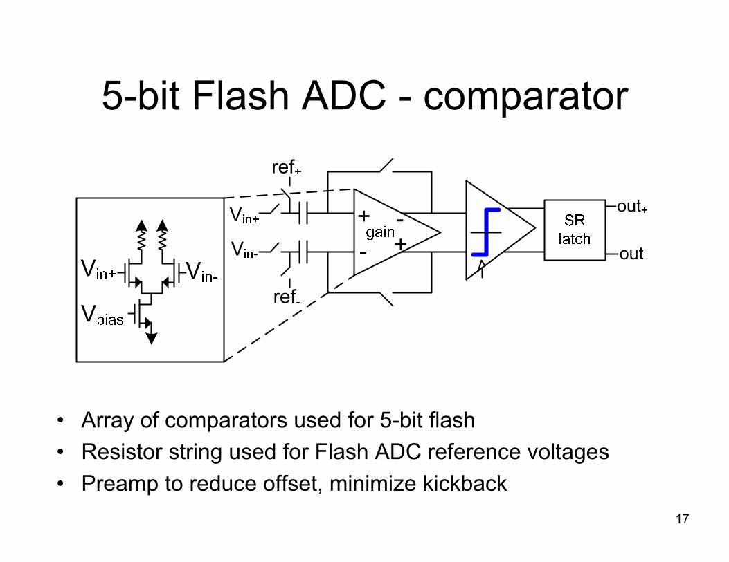
5-bit Flash ADC - comparator
• Array of comparators used for 5-bit flash• Resistor string used for Flash ADC reference voltages• Preamp to reduce offset, minimize kickback
18
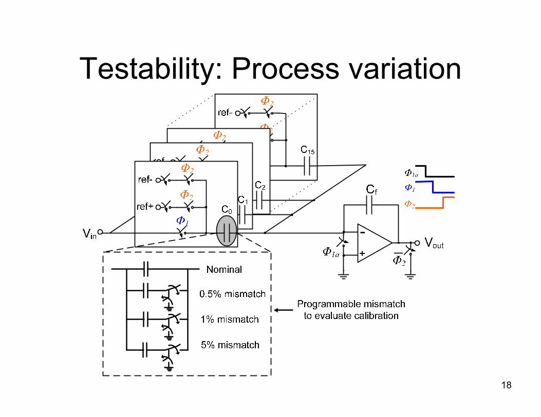
Testability: Process variation

19
0.18µm CMOS Chip Micrograph
• Area = 3.57mm2
• Power = 81mW (analog core)
20
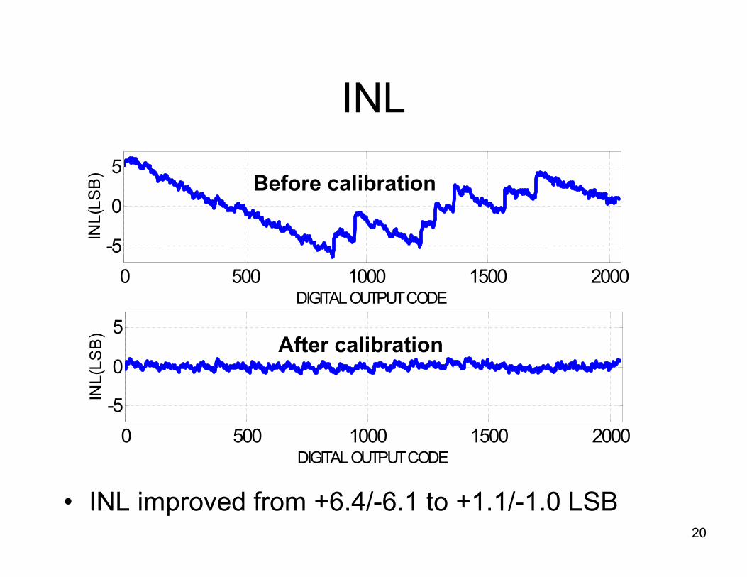
INL
• INL improved from +6.4/-6.1 to +1.1/-1.0 LSB
0 500 1000 1500 2000-5
0
5
DIGITAL OUTPUT CODE
INL(
LSB
)
0 500 1000 1500 2000-5
0
5
DIGITAL OUTPUT CODE
INL(
LSB
)

21
FFT
0 5 10 15 20-100
-50
00 5 10 15 20-100
-50
0
in
22
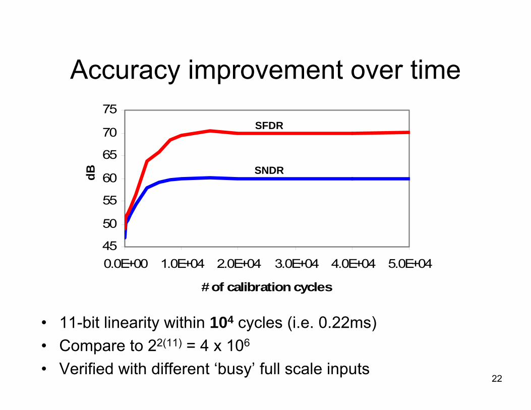
Accuracy improvement over time
• 11-bit linearity within 104 cycles (i.e. 0.22ms)• Compare to 22(11) = 4 x 10⁶
• Verified with different ‘busy’ full scale inputs
45
50
55
60
65
70
75
0.0E+00 1.0E+04 2.0E+04 3.0E+04 4.0E+04 5.0E+04
# of calibration cycles
SFDR
SNDRdB

23
Performance summary
104 cycles, (0.22ms)# calibration cycles
3.57mm2Area
81mWPower (analog core)
6046.9SNDR
7048.9SFDR (dB)
+1.1/-1.0+6.4/-6.1INL (LSB)
After CalibrationBefore calibration
fs=45MS/s (fin=2.39MHz)

24
Conclusions• Presented architecture to rapidly correct
DAC and gain errors in multi-bit pipeline stage
• Measured results in 0.18µm CMOS show linearity improved by >3b within 104 clock cycles
• Calibration achieved in more than two order of magnitude fewer clock cycles than prior statistical approaches

25
Acknowledgements• Feedback from Professor Ken Martin, University of
Toronto
• The generous funding from the National Sciences and Research Council of Canada (NSERC)
• The fabrication services of the Canadian Microelectronic Corporation (CMC)