Embed Size (px)
Citation preview

General DescriptionThe MAX6972/MAX6973 precision current-sinking, 16-output PWM LED drivers drive red, green, and/or blueLEDs for full-color graphic message boards and videodisplays. Each output has an individual 12-bit (MAX6972)or 14-bit (MAX6973) PWM-intensity (hue) control and 7-bit (MAX6972) or 5-bit (MAX6973) global PWM intensity(luminance) control. The MAX6972/MAX6973 also fea-ture open-circuit LED fault-detection circuitry, as well asa watchdog timer.
The driver has two banks of eight outputs, with each bankintended to drive a different color in RGB applications.The standard application uses three MAX6972/MAX6973s to drive eight RGB LEDs. The full-scale currentfor each bank of eight outputs is adjustable from 11mAto 55mA in 256 steps (0.3125% per step) to calibrateeach color.
The MAX6972/MAX6973 can optionally multiplex byusing outputs MUX0 and MUX1, which each drive anexternal pnp transistor. Multiplexing doubles theMAX6972/MAX6973 drive capability to 32 LEDs.
The MAX6972/MAX6973 operate from a 3.0V to 3.6Vpower supply. The LED power supply can range from3V to 7V. The LED drivers require only 0.8V headroomabove the LEDs’ forward-voltage drop. Using a sepa-rate LED supply voltage for each LED minimizes powerconsumption.
The serial interface uses differential signaling for thehigh-speed clock and data signals to reduce EMI andimprove signal integrity. The MAX6972/MAX6973 bufferall interface signals to simplify cascading devices inmodules that use a large number of drivers.
An internal watchdog timer, when enabled, automaticallyclears the pixel-data registers and blanks the display ifany of the signal inputs fail to toggle within 40ms.
The MAX6972/MAX6973 are available in 32-pin TQFNpackages and operate over the -40°C to +125°Ctemperature range.
Refer to the MAX6974/MAX6975 data sheet for a24-output, 6mA to 30mA software-compatible device.EZCascade is a trademark of Maxim Integrated Products, Inc.
ApplicationsLED Video Display Panels
LED Message Boards
Variable Message Signs (VMS)
Signs
Graphic Panels
Features♦ 16 LED Current Sink Outputs (Two Banks of Eight
Outputs)♦ 32 LED Drive Option When Multiplexing♦ 33MHz Clock Supports Up to 63 Frames per
Second of Video♦ Constant Output Current Calibration from 11mA
to 55mA in 256 Steps♦ EZCascade™ Interface Simplifies Multiple Driver
Cascading Without External Buffers♦ 12-Bit or 14-Bit Individual PWM LED Intensity
Controls♦ 7-Bit or 5-Bit Panel PWM-Intensity Control♦ +3V to +7V LED Power Supply♦ +3.0V to +3.6V Logic Supply♦ Open-Circuit LED Fault Detection♦ Optional Watchdog Timer Blanks Display if
Interface Fails♦ Standard -40°C to +125°C Operating Temperature
Range
MA
X6
97
2/M
AX
69
73
16-Output PWM LED Driversfor Message Boards
________________________________________________________________ Maxim Integrated Products 1
MAX6972ATJMAX6973ATJ
TQFN5mm x 5mm
TOP VIEW
29
30
28
27
12
11
13
MUX
0
CLKI
-
DIN+
DIN-
LOAD
I
14
V DD
MUX
1
CLKO
-
DOUT
+
AGND
DOUT
-
LOAD
0
1
+
2
Z4
4 5 6 7
2324 22 20 19 18
Z3
Z2
Y5
Y4
Y3
Y2
CLKI
+CL
KO+
3
21
31 10Z1 Y1
32 9Z0 Y0
Z5
26 15 Y6Z6
25 16 Y7
EP*
*EP = EXPOSED PADDLE.
I.C.
V DD
8
17
Z7
Pin Configuration
Ordering Information
19-0534; Rev 0; 5/06
For pricing delivery, and ordering information please contact Maxim/Dallas Direct! at 1-888-629-4642, or visit Maxim’s website at www.maxim-ic.com.
EVALUATION KIT
AVAILABLE
PART TEMP RANGEPIN-PACKAGE
PKGCODE
MAX6972ATJ+ -40°C to +125°C 32 TQFN-EP* T3255-5
MAX6973ATJ+ -40°C to +125°C 32 TQFN-EP* T3255-5
Typical Operating Circuit appears at the end of data sheet.
*EP = Exposed paddle.
+Denotes lead-free package.
MA
X6
97
2/M
AX
69
73
16-Output PWM LED Driversfor Message Boards
2 _______________________________________________________________________________________
ABSOLUTE MAXIMUM RATINGS
Stresses beyond those listed under “Absolute Maximum Ratings” may cause permanent damage to the device. These are stress ratings only, and functionaloperation of the device at these or any other conditions beyond those indicated in the operational sections of the specifications is not implied. Exposure toabsolute maximum rating conditions for extended periods may affect device reliability.
(All voltages with respect to GND.)VDD........................................................................-0.3V to +4.0VY0–Y7, Z0–Z7, MUX0, and MUX1 .........................-0.3V to +8.0VAll Other Pins..............................................-0.3V to (VDD + 0.3V)Continuous Power Dissipation (TA = +70°C)
32-Pin TQFN (derate 34.5mW/°C over +70°C) ..........2857mW
Operating Temperature Range .........................-40°C to +125°CJunction Temperature ......................................................+150°CStorage Temperature Range .............................-65°C to +150°CLead Temperature (soldering, 10s) .................................+300°C
PARAMETER SYMBOL CONDITIONS MIN TYP MAX UNITS
Operating Supply Voltage VDD 3.0 3.6 V
LEDs Anode Voltage(Y0–Y7, Z0–Z7, MUX0, and MUX1)
VO 7 V
fCLKI = 0Hz; CLKO_, DOUT_ loaded 200Ω;calibration DACs set to 0x01
21 35
fCLKI = 0Hz; CLKO_, DOUT_ loaded 200Ω;calibration DACs set to 0xFF
40 55Supply Current IDD
fCLKI = 32MHz; CLKO_, DOUT_ loaded 200Ω;calibration DACs set to 0xFF
42 60
mA
Input High Voltage LOADI VIHC0.7
x VDDV
Input Low Voltage LOADI VILC0.3
x VDDV
Differential Input Voltage RangeCLKI_, DIN_
VID ±0.15 ±1.20 V
Common-Mode Input VoltageCLKI_, DIN_
VCM | V I D / 2| 2.4 V
Differential Input High Threshold VDIFFTH 8 65 mV
Differential Input Low Threshold VDIFFTL -65 -8 mV
Differential Output VoltageCLKO_, DOUT_
VOD Termination 200Ω at receiver _+ and _- inputs ±190 ±550 mV
Differential Output OffsetCLKO_, DOUT_
VOS Termination 200Ω at receiver _+ and _- inputs 1.125 1.25 1.375 V
Input Leakage CurrentCLKI_, DIN_, LOADI
IIH, IIL -1 +1 µA
Input CapacitanceCLKI_, DIN_, LOADI
10 pF
Output Low Voltage LOADO VOLC ISINK = 5mA 0.05 0.25 V
Output High Voltage LOADO VOHC ISOURCE = 5mAVDD- 0.5
VDD- 0.2
V
Output Slew Time LOADO 20% to 80%, 80% to 20%, load = 10pF 3 ns
ELECTRICAL CHARACTERISTICS(VDD = 3.0V to 3.6V, TA = TMIN to TMAX, unless otherwise noted. Typical values are at VDD = 3.3V, TA = +85°C.) (Note 1)

MA
X6
97
2/M
AX
69
73
16-Output PWM LED Driversfor Message Boards
_______________________________________________________________________________________ 3
Note 1: All parameters tested at TA = +85°C. Specifications over temperature are guaranteed by design.
Note 2: Specification limits apply to devices at the same TA for TA = TMIN to TMAX.
Note 3: Guaranteed by design.
PARAMETER SYMBOL CONDITIONS MIN TYP MAX UNITS
Output Low Voltage MUX_ VOLM ISINK = 40mA 0.4 V
Open-Circuit Detection VOCD 200 mV
Output Slew TimeY0–Y7, Z0–Z7
80% to 20%, load = 50pF,calibration DACs set to 0xFF
100 ns
TA = +85°C 54 55 56Full-Scale Port Output CurrentY0–Y7, Z0–Z7
ISINKFSVDD = 3.3V, VO = 1.2V,calibration DACs set to 0xFF TA = TMIN to TMAX 52.5 55 58.0
mA
TA = +125°C(Note 3)
±0.5 ±1.8
TA = +85°C ±0.5 ±1.2Port-to-Port Current MatchingY0–Y7, Z0–Z7
∆ISINK
VDD = 3.3V, VO = 1.2V,calibration DACs set to 0xFFISINK = 55mA (Note 2) TA = -40°C
(Note 3)±0.7 ±2.3
%
D evi ce- to- D evi ce C ur r ent M atchi ng Y0–Y7, Z0–Z7
∆IAVGV D D = 3.3V , V O = 1.2V , cal i b r ati on D AC s set to 0xFF,ISINK = 55mA, TA = +85°C (Note 3)
±1 ±2 %
TA = +85°C 31.0 33 35.5Half-Scale Port Output CurrentY0–Y7, Z0–Z7
ISINKHSVDD = 3.3V, VO = 1.2V,calibration DACs set to 0x80 TA = TMIN to TMAX 30.0 33 36.5
mA
TA = +85°C 0.3 1.15Output Load Regulation ∆IOLR
V D D = 3.3V , V O = 1.2V to3.0V , calibration DACs set to0x80, ISINK = 33mA TA = TMIN to TMAX 1.5
mA/V
TA = +85°C 0.6 1.7Output Power-Supply Rejection ∆IOPSR
V D D = 3.0 V to 3.6V ,V O = 1.2V , calibration DACsset to 0x80, ISINK = 33mA TA = TMIN to TMAX 2.0
mA/V
ELECTRICAL CHARACTERISTICS (continued)(VDD = 3.0V to 3.6V, TA = TMIN to TMAX, unless otherwise noted. Typical values are at VDD = 3.3V, TA = +85°C.) (Note 1)
PARAMETER SYMBOL CONDITIONS MIN TYP MAX UNITS
CLKI_ Input Frequency fCLKI 33 MHz
CLKI_ Duty Cycle 40 60 %
CLKO_ Output Delay tPD-CLKO 16 ns
DIN_ Setup Time tSU-DIN 0.5 ns
DIN_ Hold Time tHD-DIN 5 ns
DOUT_ Output Delay tPD-DOUT 15 ns
LOADO Output Delay tPD-LOADO 18 ns
LOADI Setup Time tSU-LOADI -3 ns
LOADI Hold Time tHD-LOADI 8 ns
Watchdog Period When enabled 40 125 300 ms
TIMING CHARACTERISTICS(VDD = 3.0V to 3.6V, TA = TMIN to TMAX, unless otherwise noted. Typical values are at 3.3V, TA = +85°C.) (Note 1)
MA
X6
97
2/M
AX
69
73
16-Output PWM LED Driversfor Message Boards
4 _______________________________________________________________________________________
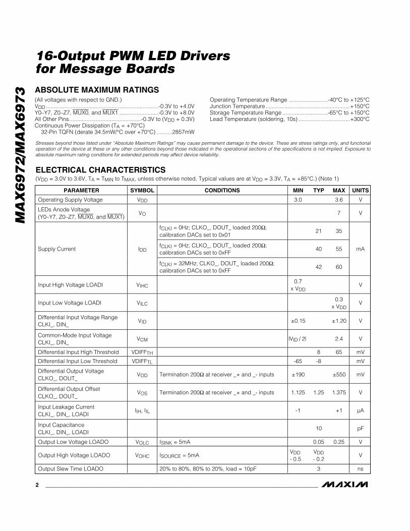
Typical Operating Characteristics(VDD = 3.3V, TA = +25°C, unless otherwise noted.)
OPERATING CURRENT CONSUMPTIONvs. SUPPLY VOLTAGE VDD
MAX
6972
/73
toc0
1
SUPPLY VOLTAGE VDD (V)
I DD
(mA)
3.53.43.33.23.1
41
43
45
47
393.0 3.6
TA = -40°C
fCLKI = 32MHzCALDAC = 0xFF
TA = +25°C
TA = +85°CTA = +125°C
OPERATING CURRENT CONSUMPTIONvs. SUPPLY VOLTAGE VDD
MAX
6972
/73
toc0
2
SUPPLY VOLTAGE VDD (V)I D
D (m
A)3.53.43.33.23.1
19
21
23
25
15
17
3.0 3.6
TA = -40°C TA = +25°C
TA = +85°CTA = +125°C
fCLKI = 0MHzCALDAC = 0x00
LED OUTPUT SINK CURRENT vs. OUTPUT VOLTAGE
MAX
6972
/73
toc0
3
OUTPUT VOLTAGE (V)
I SIN
K (m
A)
54321
20
50
60
30
40
70
0
10
0 6 7
TA = -40°C
TA = +25°CTA = +85°C
TA = +125°C
LED OUTPUT SINK CURRENT vs. OUTPUT VOLTAGE
MAX
6972
/73
toc0
4
OUTPUT VOLTAGE (V)
I SIN
K (m
A)
54321
20
50
60
30
40
70
0
10
0 6 7
VDD = +3.0V
VDD = +3.3V VDD = +3.6V

MA
X6
97
2/M
AX
69
73
16-Output PWM LED Driversfor Message Boards
_______________________________________________________________________________________ 5
Pin Description
PIN NAME FUNCTION
1,17 VDD Positive Supply Voltage. Bypass VDD to GND with a 0.1µF ceramic capacitor.
2 MUX0 Multiplex 0 Active-Low, Open-Drain Output. Use MUX0 to drive a pnp transistor.
3 CLKI+ PWM and Serial-Interface Noninverting Clock LVDS Input
4 CLKI- PWM and Serial-Interface Inverting Clock LVDS Input
5 DIN+ Serial-Interface Noninverting Data LVDS Input
6 DIN- Serial-Interface Inverting Data LVDS Input
7 LOADI Serial-Interface Load CMOS Input
8 I.C. Internally Connected. Connect to GND.
9–16 Y0–Y7 Y LED Drive Outputs. Y0 to Y7 are open-drain, constant-current sinks.
18 LOADO Serial-Interface Load CMOS Output
19 DOUT- Serial-Interface Inverting Data LVDS Output
20 DOUT+ Serial-Interface Noninverting Data LVDS Output
21 CLKO- PWM and Serial-Interface Inverting Clock LVDS Output
22 CLKO+ PWM and Serial-Interface Noninverting Clock LVDS Output
23 MUX1 Multiplex 1 Active-Low, Open-Drain Output. Use MUX1 to drive a pnp transistor.
24 AGND Analog Ground. Connect to GND.
25–32 Z7–Z0 Z LED Drive Outputs. Z0 to Z7 are open-drain, constant-current sinks.
EP GND Power Ground. Exposed pad on package underside must be connected to GND.

MA
X6
97
2/M
AX
69
73
16-Output PWM LED Driversfor Message Boards
6 _______________________________________________________________________________________
MAX6972 Block Diagram
MUX1OUTPUT
MUX0OUTPUT
Y LED DRIVERSY7–Y0
ISET
EXT. PNP
8-BITY CALDAC
Z LED DRIVERSZ0–Z7
CALIBRATIONDATA LATCH
GLOBAL-INTENSITY
DATA LATCH
PWMCOUNTERS
SYNC
CONTROL
SYNC DETECT 24-BIT NEW HEADERSHIFT REGISTER
7-BIT GLOBAL-INTENSITY FRAME MODULATOR12-BIT INDIVIDUAL INPUT MODULATOR
8
ISET8-BIT
Z CALDAC
Y LED OUTPUTY7 Y6 Y5 Y4 Y3 Y2 Y1 Y0
Z LED OUTPUTZ7 Z6 Z5 Z4 Z3 Z2 Z1 Z0
88
0/1
8
7
7
192
192 192
192 192
192
192
192
16
7
MUX0 PIXEL PWM OLD DATA LATCH MUX1 PIXEL PWM OLD DATA LATCHLOADOE
LOADOE
MUX0 PIXEL PWM NEW DATA LATCH MUX1 PIXEL PWM NEW DATA LATCH
192-BIT DATA SHIFT REGISTER
EN
CLKI
DIN
EN
DOUT
CLKO
LOADO
D Q1
LOADI
EXT. PNP
MAX6972

MA
X6
97
2/M
AX
69
73
16-Output PWM LED Driversfor Message Boards
_______________________________________________________________________________________ 7
MAX6973 Block Diagram
MUX1OUTPUT
MUX0OUTPUT
Y LED DRIVERSY7–Y0ISET
EXT. PNP
8-BITY CALDAC
Z LED DRIVERSZ0–Z7
CALIBRATIONDATA LATCH
GLOBAL-INTENSITY
DATA LATCH
PWMCOUNTERS
SYNC
CONTROL
SYNC DETECT 24-BIT NEW HEADERSHIFT REGISTER
5/3-BIT GLOBAL-INTENSITY PDM MODULATOR14-BIT INDIVIDUAL PWM MODULATOR
8
ISET8-BIT
Z CALDAC
Y LED OUTPUTY7 Y6 Y5 Y4 Y3 Y2 Y1 Y0
Z LED OUTPUTZ7 Z6 Z5 Z4 Z3 Z2 Z1 Z0
88
0/1
8
5
5
224
224 224
224 224
224
224
224
16
5
MUX0 PIXEL PWM OLD DATA LATCH MUX1 PIXEL PWM OLD DATA LATCHLOADOE
LOADOE
MUX0 PIXEL PWM NEW DATA LATCH MUX1 PIXEL PWM NEW DATA LATCH
224-BIT DATA SHIFT REGISTER
EN
CLKI
DIN
EN
DOUT
CLKO
LOADO
D Q1
LOADI
EXT. PNP
MAX6973

MA
X6
97
2/M
AX
69
73 Detailed Description
The MAX6972/MAX6973 drive 16 nonmultiplexed LEDsor 32 multiplexed LEDs for various indoor and outdoordisplay applications. The EZCascade serial interfaceenables large multidriver display panels to be con-structed with interconnected MAX6972/MAX6973devices (see Figure 1).
The drivers provide 12-bit (MAX6972) or 14-bit(MAX6973) individual PWM steps for each LED output.Four to seven global-intensity bits provide additionalpulse-density modulation (PDM) intensity control (seeTable 1). The MAX6972/MAX6973 provide 19 bits oftotal current/intensity control range per color per pixel,or 18 bits if multiplexing. The total PWM dynamic rangeencompasses gamma correction and, if desired, indi-vidual LED calibration.
LED outputs are grouped in ports (Y and Z) with eightLED outputs per port. Each port features its own cur-rent calibration control DAC (CALDAC) with 0.31%resolution to set the current. The MAX6972/MAX6973 cur-rent calibration feature allows unmatched LEDS from dif-ferent lots and manufacturers to be color matched.
Power-UpOn power-up, the MAX6972/MAX6973 set the calibrationcurrent to the minimum current for all LED outputs andclear the global-intensity PDM data, individual-intensityPWM data, and the timing counters. The displayremains blank after CLKI starts running. The watchdogfunction is inactive after power-up.
16-Output PWM LED Driversfor Message Boards
8 _______________________________________________________________________________________
HOST
CLKO
DOUT
LOADO
CLKI
DIN
LOADI
MAX6972/MAX6973
1
MAX6972/MAX6973
2
MAX6972/MAX6973
3
MAX6972/MAX6973
N
CLKI
DIN
LOADI
CLKO
DOUT
LOADO
CLKI
DIN
LOADI
CLKO
DOUT
LOADO
CLKI
DIN
LOADI
CLKO
DOUT
LOADO
CLKI
DIN
LOADI
CLKO
DOUT
LOADO
OPTIONAL FEEDBACK
Figure 1. Generic Cascaded Connection Scheme
GLOBAL PDMPART
LED DRIVEOUTPUTS
LED DRIVECURRENT
CALIBRATIONDAC RANGE DIRECT MULTIPLEXED
INDIVIDUALPWM
MAX6972 7 bits 6 bits 12 bits
5 bits 4 bitsMAX6973
16(7V rated)
55mA 11mA to 55mA
3 bits 2 bits14 bits
Table 1. Comparison of MAX6972/MAX6973

LED Intensity ControlThe MAX6972/MAX6973 provide three levels of outputcurrent control for LED drive: calibration DACs(CALDACs), global-intensity control, and individual-intensity control. The CALDACs set the port output cur-rent levels, while the global-intensity and individual-intensity controls modulate the output current on/offtimes, providing a fine-resolution control of averageoutput currents (see Figure 2). The individual-intensitycontrol operates on each output independently to seteach individual LED intensity level. The global-intensitycontrols modulate MAX6972/MAX6973 outputs simulta-neously for a uniform brightness control without affect-ing color. Using a fixed output current level that ismodulated only by on/off control leaves the LED colorunaffected while precisely controlling intensity. Finally,all outputs can be turned on and off simultaneously bysetting or clearing configuration bit D3 (PWM-ON).
Calibration DACsThe 8-bit Y and Z CALDACs set the output current levelfor all 8 outputs in the Y and Z ports, respectively (seethe MAX6972/MAX6973 Block Diagrams). The YCALDAC and Z CALDAC range from a low of 11mA(0x00) to a maximum of 55mA (0xFF), providing172µA/step of current trimming. The CALDACs areloaded by the serial interface using command 01 (seeTable 4). The Z CALDAC data is loaded first, followedby the Y CALDAC data (see the Serial Interface section).The loaded data takes effect immediately.
Global-Intensity ControlThe MAX6972/MAX6973 adjust global and individualintensities over a time period called a frame. One framerequires 219 (524,288) periods of CLKI and corre-sponds to one video-frame time. Video frames generallycontain consecutive images displayed rapidly to yielda motion picture display. Running the MAX6972/MAX6973 at fCLKI = 31.5MHz allows a video-frameupdate rate of 60fps for full-motion video (see theMAX6972 Video-Frame Timing and MAX6973 Video-Frame Timing sections).
The MAX6972/MAX6973 further divide frames into sub-frames to allow a unique combination of global- andindividual-intensity controls. The number of subframesis equal to the number of global-intensity control steps.The MAX6972 uses 128 subframes per frame innonmultiplexed mode (corresponding to 7-bit global-intensity PDM control) and 64 subframes in multiplexedmode (corresponding to 6-bit global-intensity PDMcontrol). The MAX6973 features 5-, 4-, 3-, and 2-bitglobal-intensity control to yield 32, 16, 8, and 4 sub-frames per frame, respectively.
The MAX6972/MAX6973 control global intensity bydriving subframes on and off. When a subframe is on, itallows the individual PWM intensity control to be drivenon the outputs. Subframes that are off do not have anyPWM modulation on the outputs.
MA
X6
97
2/M
AX
69
73
16-Output PWM LED Driversfor Message Boards
_______________________________________________________________________________________ 9
10
20
30
50
(mA)CALDAC
CURRENT
40
55mA MAX
11mA MIN
1270 GLOBAL= 96
GLOBAL-INTENSITYPDM
INDIVIDUAL-INTENSITYPWM
40950 Yn or Zn PWM= 2560
Yn or Zn IAVE = 18.750mA
CALDAC = 169
2550
40mA
100%
0%
50%
100%
0%
50%
100%
0%
50%
Figure 2. Relationship Among the CALDACs, Global-Intensity, and Individual-Intensity PWM Controls
MA
X6
97
2/M
AX
69
73 Individual PWM Control
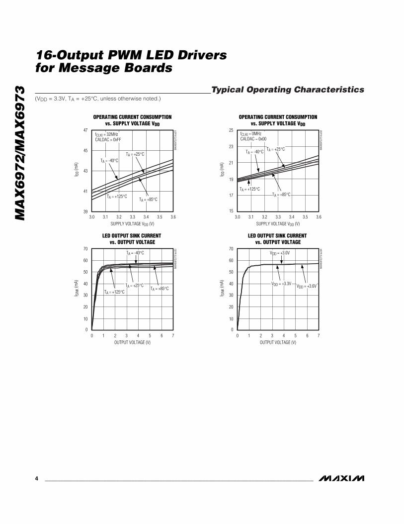
The MAX6972/MAX6973 further modulate the time thateach subframe is ON by a pulse-width modulation(PWM) value. Each output current driver in the Y and Zports has a unique 12-bit (MAX6972) or 14-bit(MAX6973) PWM control value providing fine resolutionadjustment of average current output. Each bit time ofthe PWM corresponds to one period of CLKI (TCLKI).The PWM setting determines the amount of time (out ofthe total period) that the output is on. The subframeshave PWM off zones at the start (tSPWM) and end(tEPWM) of the PWM period (see Figure 3). The sub-frame period and PWM off zones are shown in Table 2for each device.
The MAX6972 subdivides each subframe by 4096 (12-bit) PWM steps and has 16 cycle off zones, leavingan active PWM region of 4064 PWM steps ranging from16 to 4079. The MAX6973 subdivides each subframe by16,384 (14-bit) PWM steps and has 32 cycle off zones,leaving an active PWM region of 16,320 PWM stepsranging from 32 to 16,351. The PWM phase for outputsY0, Y2, Y4, Y6 and Z0, Z2, Z4, Z6 use phasing with theoutputs on first and off second. Inverse phasing is usedfor outputs Y1, Y3, Y5, Y7 and Z1, Z3, Z5, Z7 to balancethe timing of loads on the LED anode power supply, asshown in Figure 3.
In multiplexed operation, the subframes are sharedbetween MUX0 and MUX1 active times, effectivelyreducing the number of subframes by 2.
LED-Intensity Control ExampleThe three levels of intensity control are shown in Figure 2for one LED output driver in a MAX6972 in nonmulti-plexed mode. As an example, the CALDAC is set to169DEC, setting the port output current level to 40mA.
16-Output PWM LED Driversfor Message Boards
10 ______________________________________________________________________________________
Y0, Y2, Y4, Y6Z0, Z2, Z4, Z6
Y1, Y3, Y5, Y7Z1, Z3, Z5, Z7
Y0, Y2, Y4, Y6Z0, Z2, Z4, Z6
Y1, Y3, Y5, Y7Z1, Z3, Z5, Z7
SUBFRAME (n) SUBFRAME (n + 1)
tSPWM
tEMUX
tEMUX
MUX0
SUBFRAME (n), MUX0 SUBFRAME (n), MUX1
MUX1
tSPWM
tSPWM tEPWM
MULTIPLEXED
NONMULTIPLEXED
tSPWM tEPWM
ON/OFF PHASING
OFF/ON PHASING
ON/OFF PHASING
OFF/ON PHASING
50% 75%
100%25%
75%75%
75% 75%
Figure 3. Multiplexed and Nonmultiplexed Output Driver Phasing and Example PWM Values
PARTSUBFRAME
(TCLKI)tSPWM(TCLKI)
tEPWM(TCLKI)
tEMUX(TCLKI)
MAX6972 4096 16 16 16
MAX6973 16,384 32 32 32
Table 2. Subframe and PWM Timing

The global-intensity PDM value is set to 96DEC, producingan even distribution of ON subframes out of the 128 pos-sible (shown in Figure 4 as subframes 1, 3, 4, 5, etc).Each subframe can be ON for a PWM duration set by theindividual PWM value. The PWM value setting of2560DEC out of 4096 (12-bit) results in a further reductionof current ON time (shown in bold trace).
The internal PDM logic spreads the on subframes asevenly as possible among the off subframes to keepthe effective scanning frequency high.
For applications with a slower clock speed, theMAX6973 can increase the display refresh rate by afactor of four to eliminate visible flicker. Setting configu-ration bit D4 (GLB4) to 1 activates the increasedrefresh rate (see Table 6). The increased refresh ratereduces the number of global-intensity settings by afactor of four (see Table 3).
MAX6972 Video-Frame TimingThe MAX6972 supports up to 60 video frames persecond (fps). The following equation shows therequired clock frequency to support 60 video fps:
60 (video fps) x 4096 (clocks per 12-bit PWM period) x128 (global-intensity subframes) = 31.5MHz.
The MAX6972 supports up to a 33MHz clock signal(~63fps).
Each 12-bit PWM period contains 4096 clock cycles;multiply that number by 128 (number of global intensitysubframes) to obtain the required number of clock cycles(524,288) per video frame. The MAX6972 requires 36bits (12 bits per color multiplied by three colors) to drivean RGB pixel. The maximum pixel data that theMAX6972 can send per video frame is 524,288 / 36 or14,563 pixels, corresponding to 2730 cascadedMAX6972s.
MAX6973 Video-Frame TimingThe MAX6973 also supports up to 60 video frames persecond (fps). The following equation shows therequired clock frequency to support 60 video fps:
60 (video fps) x 16,384 (clocks per 14-bit PWM period)x 32 (global-intensity subframes) = 31.5MHz.
The MAX6973 supports up to a 33MHz clock signal(~63fps).
Each 14-bit PWM period contains 16,384 clock cycles;multiply 16,384 by 32 (global-intensity subframes) toobtain the required number of clock cycles (524,288)per video frame. The MAX6973 requires 42 bits (14 bitsper color multiplied by three colors) to drive an RGBpixel. The maximum pixel data that the MAX6973 cansend per video frame is 524,288 / 42 or 12,483 pixels,corresponding to 2340 cascaded MAX6973s.
MA
X6
97
2/M
AX
69
73
16-Output PWM LED Driversfor Message Boards
______________________________________________________________________________________ 11
169d = 40
SUBFRAME NUMBER
10
20
30
50
55mA MAX
11mA MIN
(mA)
0 1 2 3 4 5 6 7 8 9 10 11
CALD
AC C
URRE
NT
OUTPUT LED CURRENTPWM = 2560/4096
ONE FRAME IS 219 (524,288) CLKI CYCLES LONG
GLOBAL PDM = 96/128 SUBFRAMES
ON ON ON ON ON ON ON ON
Figure 4. The three levels of LED current control (CALDAC, global-intensity PDM, and individual PWM) modulate the average outputcurrent.
MA
X6
97
2/M
AX
69
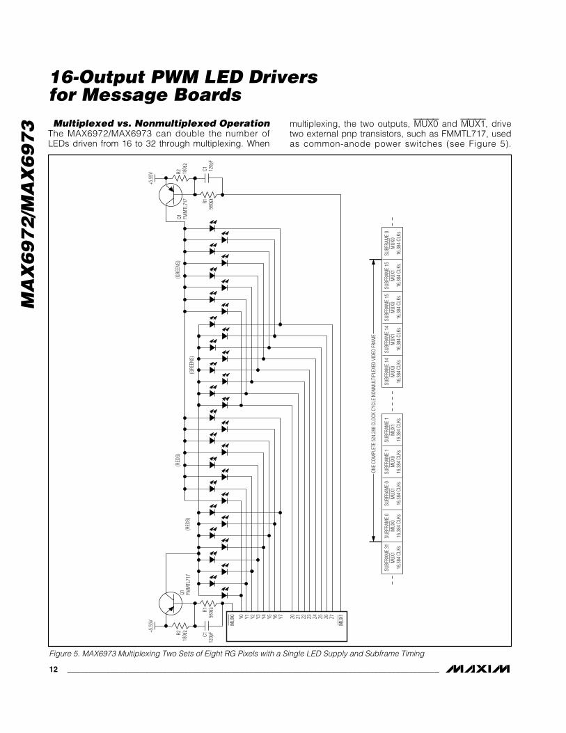
73 Multiplexed vs. Nonmultiplexed Operation
The MAX6972/MAX6973 can double the number ofLEDs driven from 16 to 32 through multiplexing. When
multiplexing, the two outputs, MUX0 and MUX1, drivetwo external pnp transistors, such as FMMTL717, usedas common-anode power switches (see Figure 5).
16-Output PWM LED Driversfor Message Boards
12 ______________________________________________________________________________________
Y0 Y1 Y2 Y3 Y4 Y5 Y6 Y7
+5.5
5V
Q1 FMM
TL71
7(R
EDS)
(RED
S)
(GRE
ENS)
(GRE
ENS)
R156
0Ω
R218
0Ω C112
0pF
+5.5
5V
Q1 FMM
TL71
7 R156
0Ω
R2 180Ω C1 12
0pF
Z1 Z2 Z3 Z4 Z5 Z6 Z7Z0
SUBF
RAM
E 31
MUX
116
,384
CLK
s
SUBF
RAM
E 0
MUX
016
,384
CLK
s
SUBF
RAM
E 0
MUX
116
,384
CLK
s
SUBF
RAM
E 1
MUX
016
,384
CLK
s
SUBF
RAM
E 1
MUX
116
,384
CLK
s
SUBF
RAM
E 14
MUX
016
,384
CLK
s
SUBF
RAM
E 14
MUX
116
,384
CLK
s
SUBF
RAM
E 15
MUX
016
,384
CLK
s
SUBF
RAM
E 15
MUX
116
,384
CLK
s
SUBF
RAM
E 0
MUX
016
,384
CLK
s
ONE
COM
PLET
E 52
4,28
8 CL
OCK
CYCL
E NO
NMUL
TIPL
EXED
VID
EO F
RAM
E
MUX
0
MUX
1
Figure 5. MAX6973 Multiplexing Two Sets of Eight RG Pixels with a Single LED Supply and Subframe Timing
Setting configuration bit D0 to 1 enables multiplexoperation. MUX0 and MUX1 alternate the LED anodedrive voltage between two sets of LEDs. The Y and Zports provide individual PWM control during alternateMUX cycles as shown in Figure 3. The alternating MUXcycles reduce the global-intensity resolution (the num-ber of subframes) by half, which reduces the averageLED current by half.
WatchdogA selectable watchdog timer monitors serial-interfaceinputs CLKI, DIN, and LOADI. Enabling the watchdogtimer requires that CLKI, DIN, and LOADI toggle atleast once every 40ms. If any of these transitions fails tooccur, then the individual-intensity PWM data latchesclear. This condition effectively blanks the LEDs.Update the individual-intensity PWM data registers toturn the LEDs back on. The watchdog timeout does notaffect the calibration or global-intensity data, the clocksynchronization, or multiplexed/nonmultiplexed setting.
Use the watchdog functionality in safety-critical appli-cations where a blanked display is safer than an incor-rect display.
LED Open-Circuit andOvertemperature Detection
The MAX6972/MAX6973 feature two fault detection func-tions: open-circuit LED outputs and overtemperature. AnLED open-circuit is detected on driver outputs by moni-toring for output voltages below 200mV. When an opencircuit is detected, the MAX6972/MAX6973 incrementsa fault counter included in the serial-interface protocolthat can be routed back to the host transmitter for diag-nostics. Any number of open-circuit LEDS, multiplexedor nonmultiplexed, can be detected, however only onecounter increment occurs per device.
The MAX6972/MAX6973 detect die temperaturesabove TDIE = +165°C and disable all output drivers bysetting all PWM data to zero. The fault counter in theserial-interface protocol is incremented by one countfor each cascaded device with an overtemperaturecondition. The output drivers are turned back on whenthe die temperature falls below TDIE = +150°C. Thefault counter value is distinguished between LED open-circuit and overtemperature conditions by the serial-interface command used at the time of detection (seethe Serial Interface section for more details).
MA
X6
97
2/M
AX
69
73
16-Output PWM LED Driversfor Message Boards
______________________________________________________________________________________ 13
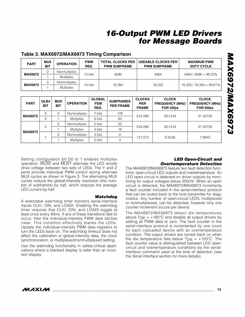
PARTMUXBIT
OPERATIONPWMRES.
TOTAL CLOCKS PERPWM SUBFRAME
USEABLE CLOCKS PERPWM SUBFRAME
MAXIMUM PWMDUTY CYCLE
0 NonmultiplexMAX6972
1 Multiplex12 bits 4096 4064 4064 / 4096 = 99.22%
0 NonmultiplexMAX6973
1 Multiplex14 bits 16,384 16,320 16,320 / 16,384 = 99.61%
Table 3. MAX6972/MAX6973 Timing Comparison
PARTGLB4BIT
MUXBIT
OPERATIONGLOBAL
PDMRES.
SUBFRAMESPER FRAME
CLOCKSPER
FRAME
CLOCKFREQUENCY (MHz)
FOR 50fps
CLOCKFREQUENCY (MHz)
FOR 60fps
X 0 Nonmultiplex 7 bits 128MAX6972
X 1 Multiplex 6 bits 64524,288 26.2144 31.45728
0 Nonmultiplex 5 bits 320
1 Multiplex 4 bits 16524,288 26.2144 31.45728
0 Nonmultiplex 3 bits 8MAX6973
11 Multiplex 2 bits 4
131,072 6.5536 7.8643

MA
X6
97
2/M
AX
69
73 Commands
The MAX6972/MAX6973 have four commands used toload all operating mode and LED output current data.Each command is uniquely identified by two bits, C1and C0, embedded in the serial-interface protocolstructure. The commands Load CALDAC, Load Global-Intensity PDM, and Load Configuration each require 16bits of data (2 bytes) for every cascaded device. Thenumber of bits required for the command load individualPWM varies by device and multiplex mode of operation.Each cascaded device can receive unique data forCALDACs, global intensity, configuration, and individualPWM output drivers. Generally, all cascaded devicesare operated in the same configuration mode. The databytes are transmitted MSB first for all commands. Thecommands are communicated to all cascaded devicesby the host using the synchronous serial-interface andprotocol structure (see the Serial Interface section fordetails). The four commands and the data lengths foreach command are shown in Table 4.
The MAX6972, operating in nonmultiplexed mode,requires sixteen 12-bit individual PWM data (192 bitstotal) and requires thirty-two 12-bit data (384 bits total)in multiplexed operation mode. Similarly, the MAX6973operating in nonmultiplexed mode requires sixteen 14-bitindividual-intensity PWM data (224 bits total) andrequires thirty-two 14-bit (448 bits total) data in multi-
plexed mode. The individual PWM data are loaded intoan intermediate latch and transferred to the actualPWM latches at subframe 0 and PWM clock 0.
Both Y and Z calibration DACs are loaded with 8-bitdata each in nonmultiplexed and multiplexed modes.Data is updated immediately into the CALDAC latches(see Table 8).
The MAX6972/MAX6973 require one data byte to set theglobal-intensity PDM for all output drivers. The global-intensity PDM data has a variable number of active bitsdepending on the multiplex operating mode and, forthe MAX6973, the global-quarter setting. The number ofbits used for global-intensity control is always justifiedto the LSB of the data byte, as shown in Table 5. Onebyte of data is sent twice with the global-intensity PDMdata bits justified to the LSB. Data is updated into thePWM latches at subframe 0 and PWM clock 0 (seeTable 9).
When using the MAX6973 5-bit global-intensity setting,the settings range from 0 to 63 to set the global intensityfrom 1 to 64 subframes ON to 64 out of 64 subframes ON.When using the MAX6972 7-bit global-intensity setting,the settings range from 0 to 127 to set the global inten-sity from 1 out of 128 subframes ON to 128 out of 128subframes ON.
16-Output PWM LED Driversfor Message Boards
14 ______________________________________________________________________________________
CMD[1:0]
C1 C0COMMAND DATA LENGTH PER CASCADED DEVICE
192 bits (MAX6972 nonmultiplexed)
384 bits (MAX6972 multiplexed)
224 bits (MAX6973 nonmultiplexed)0 0 Load individual PWM
448 bits (MAX6973 multiplexed)
0 1 Load CALDAC 16 bits
1 0 Load global-intensity PDM 16 bits
1 1 Load configuration 16 bits
Table 4. Commands and Data Length
PART GLB4 MUX TOTAL BITS MSB D7 D6 D5 D4 D3 D2 D1 LSB D0
X 0 7 0 Bit[6] Bit[5] Bit[4] Bit[3] Bit[2] Bit[1] Bit[0]MAX6972
X 1 6 0 0 Bit[5] Bit[4] Bit[3] Bit[2] Bit[1] Bit[0]
0 0 5 0 0 0 Bit[4] Bit[3] Bit[2] Bit[1] Bit[0]
0 1 4 0 0 0 0 Bit[3] Bit[2] Bit[1] Bit[0]
1 0 3 0 0 0 0 0 Bit[2] Bit[1] Bit[0]MAX6973
1 1 2 0 0 0 0 0 0 Bit[1] Bit[0]
Table 5. Global-Intensity Data Bit Justification

The global-intensity data is received in an intermediateregister and is applied to the outputs at subframe 0 andPWM clock 0.
The MAX6972/MAX6973 have one byte of configurationdata with 5 active bit settings as shown in Table 6. Onebyte of data containing configuration bit settings is senttwice. Data is updated immediately into the CALDAClatches. See Table 10. The loaded configuration settingstake effect immediately.
Serial InterfaceThe MAX6972/MAX6973 feature a fully synchronousand fully buffered serial interface that allows cascadingof multiple devices. The serial interface consists ofinputs (CLKI, DIN, and LOADI) and outputs (CLKO,DOUT, and LOADO). The MAX6972/MAX6973 canpass different data to each cascaded device withoutany additional inputs to identify the position of thedevices in the cascaded chain.
MA
X6
97
2/M
AX
69
73
16-Output PWM LED Driversfor Message Boards
______________________________________________________________________________________ 15
CONFIGURATION BIT ACRONYM FUNCTION DESCRIPTION
MSB D7 — 0 Not used
D6 — 0 Not used
D5 — 0 Not used
D4 GLB4 Global quarter
Enables the reduced global-intensity setting in the MAX6973 when set to1. When set, the MAX6973 uses eight (or four, if multiplexing) PWMsubframes. GLB4 is set to 0 as power-on default. Setting bit D4 has noeffect in the MAX6972.
D3 PWM-ONEnable
individualPWMs
Turns all individual PWM outputs on when set to 1. Power-on default isPWM-ON set to 0 to disable all current output drivers. PWM-ON can beused to turn all LEDs on or off without affecting the global-intensity orindividual PWM settings.
D2 CRSTReset frameand PWMcounters
Setting CRST to 1 synchronously resets internal counters to 0. This actionsets the MAX6972/MAX6973 to subframe 0 of the global-intensitysubframe counter and clock 0 of all individual PWM counters. The CRSTbit is a nonlatching control function that resets to 0 after the counters areset to 0.
D1 WDOGWatchdog
enableSetting WDOG to 1 enables the watchdog timer operation. Power-ondefault is 0.
LSB D0 MUXMultiplexenable
Setting MUX to 1 turns multiplex mode on. Power-on default is 0.
Table 6. Load Configuration Bit Definitions
MA
X6
97
2/M
AX
69
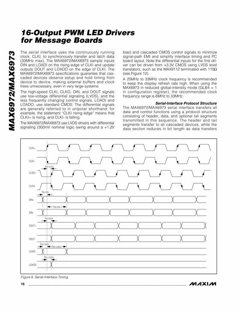
73 The serial interface uses the continuously running
clock, CLKI, to synchronously transfer and latch data(33MHz max). The MAX6972/MAX6973 sample inputsDIN and LOADI on the rising edge of CLKI and updateoutputs DOUT and LOADO on the edge of CLKI. TheMAX6972/MAX6973 specifications guarantee that cas-caded devices observe setup and hold timing fromdevice to device, making external buffers and clocktrees unnecessary, even in very large systems.
The high-speed CLKI, CLKO, DIN, and DOUT signalsuse low-voltage differential signaling (LVDS), and theless frequently changing control signals, LOADI andLOADO, use standard CMOS. The differential signalsare generally referred to in unipolar shorthand; forexample, the statement “CLKI rising edge” means thatCLKI+ is rising, and CLKI- is falling.
The MAX6972/MAX6973 use LVDS drivers with differentialsignaling (300mV nominal logic swing around a +1.2V
bias) and cascaded CMOS control signals to minimizesignal-path EMI and simplify interface timing and PCboard layout. Note the differential inputs for the first dri-ver can be driven from +3.3V CMOS using LVDS leveltranslators, such as the MAX9112 terminated with 110Ω(see Figure 12).
A 25MHz to 33MHz clock frequency is recommendedto keep the display refresh rate high. When using theMAX6973 in reduced global-intensity mode (GLB4 = 1in configuration register), the recommended clock frequency range is 6MHz to 33MHz.
Serial-Interface Protocol StructureThe MAX6972/MAX6973 serial interface transfers alldata and control functions using a protocol structureconsisting of header, data, and optional tail segmentstransmitted in this sequence. The header and tail segments transfer to all cascaded devices, while thedata section reduces in bit length as data transfers
16-Output PWM LED Driversfor Message Boards
16 ______________________________________________________________________________________
tHD-DIN
tHD-LOADI
CLKI+
CLKI-
CLKO+
CLKO-
DIN+
DIN-
DOUT+
DOUT-
LOADI
LOADO
tPD-CLKO
tSU-DIN
tPD-DOUT
tPD-LOADO
tSU-LOADI
Figure 6. Serial-Interface Timing

through the cascaded devices. When LOADI is low, theMAX6972/MAX6973 continuously monitor DIN forreception of the SYNC pattern (see the HeaderSegment section).
Header SegmentThe 24-bit header segment consists of an 8-bit fixedsynchronization pattern (SYNC), a 6-bit command pat-tern (CMD), and a 10-bit counter (CNTR) segment (seeTable 7). LOADI must change from low to high withinplus or minus one clock cycle of the first command bit.When the SYNC bit pattern 0xE8 is recognized, LOADIis monitored for the rising edge, allowing the device tointernally synchronize LOADI to CLKI. The six commandbits, CMD[5:0], consist of bits C1 and C0 repeatedthree times. The four commands used by the MAX6972/MAX6973 are defined by the two bits, C1 and C0.The counter segment is incremented by one for eachcascaded device with an internal fault detected. Use thecounter segment to collect fault data across the cas-caded chain.
HDR[23:0]Complete 24-bit header segment.
SYNC[7:0]Synchronization bit pattern 0xE8 is recognized by theMAX6972/MAX6973 during intervals when LOADI is low.The SYNC bit pattern, followed by the rising edge ofLOADI, internally synchronizes the timing relationship
between CLKI and DIN with the LOADI signal. Thesynchronization pattern must be 0xE8.
CMD[5:0]Send command bits C1 and C0 three times in succes-sion. The command bits define how many data bits arereceived and where the data is loaded. The four com-mands are:
CNTR[9:0]This is the counter for open LED or overtemperature faultconditions. The host sends the header segment with thecounter value set to zero. The counter value is incre-mented one count by each device that detects a faultcondition in the cascaded chain. The accumulated countvalue returns to the host from the last device in the cas-cade chain. The command determines which fault typeis incremented to the counter (see LED Open-Circuit andOvertemperature Detection Counter section):
CMD[1:0] = X0 Overtemperature faults counted
CMD[1:0] = X1 Open LED faults counted
MA
X6
97
2/M
AX
69
73
16-Output PWM LED Driversfor Message Boards
______________________________________________________________________________________ 17
HDR
23 22 21 20 19 18 17 16 15 14 13 12 11 10 9 8 7 6 5 4 3 2 1 0
SYNC CMD CNTR
7 6 5 4 3 2 1 0 1 0 1 0 1 0 9 8 7 6 5 4 3 2 1 0
1 1 1 0 1 0 0 0 C1 C0 C1 C0 C1 C0 b9 b8 b7 b6 b5 b4 b3 b2 b1 b0
Table 7. Serial-Interface Header
C1:C0 COMMAND CMD[5:0]
00 Load individual PWM 000000
01 Load CALDAC 010101
10 Load global-intensity PDM 101010
11 Load configuration 111111
HEADER
COUNTER
CLKI
COMMAND
1 1 1 0 1 0 0 0
SYNC
LOADI
1 2 3 4 5 6 7 8 9 10 11 12 13 14 15 16 17 18 19 20 21 22 23 24 25 26 27 28
DIN
1
0
(CONTINUOUS)
C1 C0 C1 C0 C1 C0b9 b8 b7 b6 b5 b4 b3 b2
DATA
b1 b0
Figure 7. Header-Segment Timing

MA
X6
97
2/M
AX
69
73 Data Segment
The bit length of the data segment received by theMAX6972/MAX6973 is dependent on the commandspecified in the header.
The load CALDAC command has two unique databytes, while load global-intensity PDM and loadconfiguration each have one byte of data repeatedonce. The CALDAC data within the command loadCALDAC is sent with Z CALDAC data first followed byY CALDAC data, as shown in Table 8.
The data segment of the load individual PWM commandhas a variable length depending on specific device andconfiguration settings. The data is always organized
as Z driver data first in the order of Z7 first to Z0 last(MSB first), followed by the Y driver data in the sameorder of Y7 to Y0 (MSB first).
Tail SegmentThe MAX6972/MAX6973 allow for an optional string ofdata bits to be transmitted following all device databits, which is referred to as the tail segment. The databits of the tail segment are clocked back to the host, following the header, from the last device in a cascadedchain. The number of bits in the tail segment is optional.The tail carries no device-specific data on DIN, but provides feedback confirmation to the host that all databits were extracted by all devices in the cascade chain.
16-Output PWM LED Driversfor Message Boards
18 ______________________________________________________________________________________
HEADER DATA 1 DATA 2 DATA 3 … DATA N
HDR[23:0] Z[7:0] Y[7:0] Z[7:0] Y[7:0] Z[7:0] Y[7:0] … Z[7:0] Y[7:0]
Table 8. Serial Format for Load CALDAC
HEADER DATA 1 DATA 2 DATA 3 … DATA N
HDR[23:0] D[7:0] D[7:0] D[7:0] D[7:0] D[7:0] D[7:0] … D[7:0] D[7:0]
Table 9. Serial Format for Load Global-Intensity PDM
HEADER DATA 1 DATA 2 DATA 3 … DATA N
HDR[23:0] D[7:0] D[7:0] D[7:0] D[7:0] D[7:0] D[7:0] … D[7:0] D[7:0]
Table 10. Serial Format for Load Configuration
HEADER DATA 1 DATA 2 DATA 3 … DATA N
HDR[23:0] Z7, Z6, …Y0 Z7, Z6, …Y0 Z7, Z6, …Y0 … Zn…Yn
Table 11. Serial Format for Load Individual PWM (Nonmultiplexed)
HEADER DATA 1 DATA 2 DATA 3 … DATA N
HDR[23:0] Z7, Z7', Z6, Z6', …Y0' Z7, Z7', Z6, Z6', …Y0' Z7, Z7', Z6, Z6', …Y0' … Z7, Z7', Z6, Z6', …Y0'
Table 12. Serial Format for Load Individual PWM (Multiplexed)
Z[7:0] 8-bit data loaded into port Z CALDACY[7:0] 8-bit data loaded into port Y CALDACN Number of cascaded devices
D[7:0] Send the same data repeated (16 total bits) for the 8-bit data for global-intensity PDMSend the 8-bit data for the global-intensity PDM twice (16 total bits)
D[7:0] Send the same data repeated (16 total bits) for the 8-bit data for configurationSend the 8-bit configuration data two times (16 total bits)
Z_…Y_ 12-bit (MAX6972) or 14-bit (MAX6973) data each
Z_ 12-bit (MAX6972) or 14-bit (MAX6973) PWM data for each output Z_ during multiplex phase MUX0, MSB firstZ_' 12-bit (MAX6972) or 14-bit (MAX6973) PWM data for each output Z_ during multiplex phase MUX1, MSB firstY_ 12-bit (MAX6972) or 14-bit (MAX6973) PWM data for each output Y_ during multiplex phase MUX0, MSB firstY_' 12-bit (MAX6972) or 14-bit (MAX6973) PWM data for each output Y_ during multiplex phase MUX1, MSB first

Serial-Interface Cascade TimingThe MAX6972/MAX6973 serial-interface protocol timingis simplified by the guaranteed setup and hold charac-teristics of the outputs from one device driving theinputs of another. An example of a cascade of threeMAX6972/MAX6973 devices is shown in Figure 8.
Example of Serial-InterfaceCascade Timing
The basic timing of a MAX6972/MAX6973 cascadedchain of three devices demonstrates the principle thatapplies to any number of cascaded devices. The firstdevice connected to the host transmitter is referencedas 1, and the remaining devices are referenced as 2and 3. Device 3 outputs connect to the host for commu-nicating diagnostic and fault counter data.
The first MAX6972/MAX6973, device 1, receives theheader and captures the first set of data bits. Thenumber of captured bits is determined by the commandgiven in the header. A timing example of the data trans-fer for the Load CALDAC command is shown in Figure9. Device 1 does not send the captured data out onDOUT. Instead, device 1 sends out a new header 17clock cycles after the reception of the first header bit onDIN. The data flow on each interconnect node is shownin Figure 10.
After capturing the first data set, device 1 transmits allfollowing data segments and the optional tail segmenton DOUT, delayed by one CLKI cycle. Device 2receives the new header from device 1, followed bydata that now begins with device 2’s data set. Device 2repeats the same process as described above; captur-ing the first data set received, appending a new head-er, and passing all subsequent data out DOUT to thenext device 3. Device 3 captures the last data set andtransmits a header followed by the tail segment. Thelast header and tail segments are clocked back into thehost receiver. The header received by the host containsthe updated fault counter data. The tail data bit patterncan be compared to the tail data originally transmittedby the host for data integrity check.
When the MAX6972/MAX6973 send individual-intensityPWM data, the data segment bit length is large due to
MA
X6
97
2/M
AX
69
73
16-Output PWM LED Driversfor Message Boards
______________________________________________________________________________________ 19
HOST
CLKO
DOUT
LOADO
CLKI
DIN
LOADI
CLK0
D0
LOAD0
CLK1
D1
LOAD1
CLK2
D2
LOAD2
CLK3
D3
LOAD3
MAX6972/MAX69731
MAX6972/MAX69732
MAX6972/MAX69733
CLKI
DIN
LOADI
CLKO
DOUT
LOADO
CLKI
DIN
LOADI
CLKO
DOUT
LOADO
CLKI
DIN
LOADI
CLKO
DOUT
LOADO
Figure 8. Example Showing Three-Device Cascade Connection Scheme with the Interconnecting Nodes Labeled for Clarity
DATA: CALDAC DATA 1
(CONTINUOUS) 25 26 27 28 29 30 31 32 33 34 35 36 37 38 39 40 41 42 43 44 45 46 47 48 49 50 51 52 53 54 55 56 57 58 59 60 61 62 63 64 65 66 67 68 69 70 71 72
CLKI
LOADI
DIN
0
1
DATA: CALDAC DATA 2Z CALDAC Y CALDAC Z CALDAC Y CALDAC Z CALDAC Y CALDAC
DATA: CALDAC DATA 3
D7 D6 D5 D4 D3 D2 D1 D0 D7 D6 D5 D4 D3 D2 D1 D0 D7 D6 D5 D4 D3 D2 D1 D0 D7 D6 D5 D4 D3 D2 D1 D0 D7 D6 D5 D4 D3 D2 D1 D0 D7 D6 D5 D4 D3 D2 D1 D0
Figure 9. Timing Example Showing CALDAC Data Set for Three Cascaded Devices
WORD 1 WORD 2 WORD 3HEADER 1 T
WORD 2 WORD 3HEADER 2 T
WORD 3HEADER 3 T
HEADER 4 T
17 CLOCKS
17 CLOCKS
17 CLOCKS
CLK0
D0
D1
D2
D3
Figure 10. Data Cascading Example for 16-Bit Data Words
MA
X6
97
2/M
AX
69
73 the 12-bit or 14-bit PWM data for each of the 16 outputs
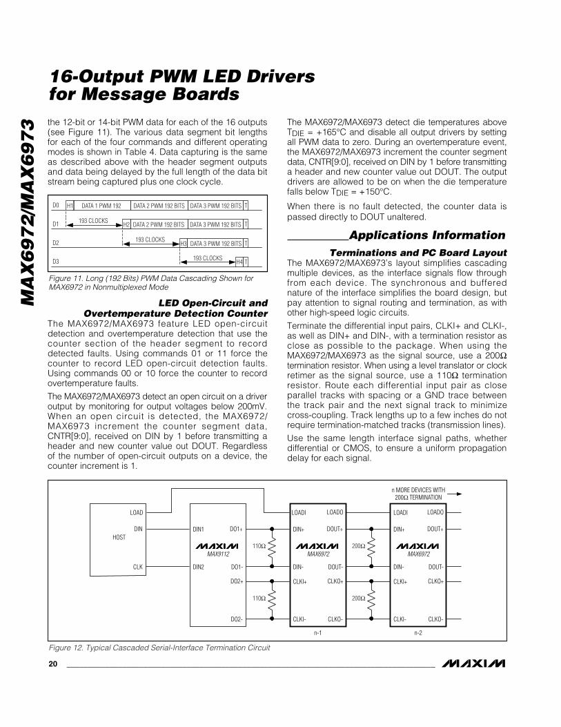
(see Figure 11). The various data segment bit lengthsfor each of the four commands and different operatingmodes is shown in Table 4. Data capturing is the sameas described above with the header segment outputsand data being delayed by the full length of the data bitstream being captured plus one clock cycle.
LED Open-Circuit andOvertemperature Detection Counter
The MAX6972/MAX6973 feature LED open-circuitdetection and overtemperature detection that use thecounter section of the header segment to recorddetected faults. Using commands 01 or 11 force thecounter to record LED open-circuit detection faults.Using commands 00 or 10 force the counter to recordovertemperature faults.
The MAX6972/MAX6973 detect an open circuit on a driveroutput by monitoring for output voltages below 200mV.When an open circuit is detected, the MAX6972/MAX6973 increment the counter segment data,CNTR[9:0], received on DIN by 1 before transmitting aheader and new counter value out DOUT. Regardlessof the number of open-circuit outputs on a device, thecounter increment is 1.
The MAX6972/MAX6973 detect die temperatures aboveTDIE = +165°C and disable all output drivers by settingall PWM data to zero. During an overtemperature event,the MAX6972/MAX6973 increment the counter segmentdata, CNTR[9:0], received on DIN by 1 before transmittinga header and new counter value out DOUT. The outputdrivers are allowed to be on when the die temperaturefalls below TDIE = +150°C.
When there is no fault detected, the counter data ispassed directly to DOUT unaltered.
Applications InformationTerminations and PC Board Layout
The MAX6972/MAX6973’s layout simplifies cascadingmultiple devices, as the interface signals flow throughfrom each device. The synchronous and bufferednature of the interface simplifies the board design, butpay attention to signal routing and termination, as withother high-speed logic circuits.
Terminate the differential input pairs, CLKI+ and CLKI-,as well as DIN+ and DIN-, with a termination resistor asclose as possible to the package. When using theMAX6972/MAX6973 as the signal source, use a 200Ωtermination resistor. When using a level translator or clockretimer as the signal source, use a 110Ω terminationresistor. Route each differential input pair as close parallel tracks with spacing or a GND trace betweenthe track pair and the next signal track to minimizecross-coupling. Track lengths up to a few inches do notrequire termination-matched tracks (transmission lines).
Use the same length interface signal paths, whetherdifferential or CMOS, to ensure a uniform propagationdelay for each signal.
16-Output PWM LED Driversfor Message Boards
20 ______________________________________________________________________________________
DATA 1 PWM 192H1
193 CLOCKS
193 CLOCKS
193 CLOCKS
D0
D1
D2
D3
DATA 2 PWM 192 BITS DATA 3 PWM 192 BITS T
DATA 2 PWM 192 BITS DATA 3 PWM 192 BITS TH2
DATA 3 PWM 192 BITS TH3
TH4
Figure 11. Long (192 Bits) PWM Data Cascading Shown forMAX6972 in Nonmultiplexed Mode
CLKI- CLKO-
CLKO+CLKI+
200Ω
DIN- DOUT-
DOUT+DIN+
LOADOLOADI
n-2
200ΩMAX6972
CLKI- CLKO-
CLKO+CLKI+
110Ω
DIN- DOUT-
DOUT+DIN+
LOADOLOADI
n-1
110ΩMAX6972
DO2-
DO2+
DIN2 DO1-
DO1+DIN1
MAX9112
CLK
DIN
LOAD
HOST
n MORE DEVICES WITH200Ω TERMINATION
Figure 12. Typical Cascaded Serial-Interface Termination Circuit

MA
X6
97
2/M
AX
69
73
16-Output PWM LED Driversfor Message Boards
______________________________________________________________________________________ 21
Power-Supply ConsiderationsThe MAX6972/MAX6973 operate with a power-supplyvoltage of 3.0V to 3.6V. Bypass the VDD power supplyto GND with a 0.1µF ceramic capacitor as close aspossible to the device pins. If the LED supply is sharedwith the VDD supply, adequately decouple the VDDsupply with bulk capacitance to ensure that the fast-rising, high-current LED drive currents do not causetransient dips in VDD.
Driving LEDs from a Supply Higher than 7VAn external npn transistor in a cascode configurationextends the output drive voltage above 7V. The externalpass transistor’s emitter clamps to a VBE below itsbase, which is connected to the MAX6972/MAX6973’ssupply voltage. An optional emitter resistor reduces thevoltage drop across the MAX6972/MAX6973’s outputtransistor and effectively takes the dissipation off thedevice into the resistor. The external transistor’s collectorcurrent is equal to its emitter current (less a small basecurrent), and the MAX6972/MAX6973 accuratelycontrol the emitter current with a constant current sinkdriver structure.
Example of using an external npn transistor:
VDD = 3.3V ±5%, IOUT = 55mA, external pass transistorVBE = 0.7V - 1V at 55mA emitter current.
For best output current accuracy, design VO to be atleast 1.2V:
R1(MAX) = (3.15 - 1 - 1.2) / 0.055 = 17.3Ω, so chooseR1 = 15Ω
hence,
VO(MIN) = 3.15 - 1 - (15 x 0.055) = 1.325V and VO(MAX)= 3.45 - 0.7 - (15 x 0.055) = 1.925V.
MAX6972MAX6973
VDD
R1
Q1
55mA
+3.3V +3.3V +24V
Y1Y2Y3Y4Y5Y6Y7
Y0
GND
Figure 13. External Cascode npn Transistor
MAX6972 MAX6972 MAX6972SYSTEMCLK
DATA
LOAD
CLKO
DINO
LOADO
CLKI
DINI
LOADI
Y0/Z0
16 RG LEDs 16 BLUE LEDs
Y1/Z1
Y2/Z2
Y3/Z3
Y4/Z4
Y5/B5
Y6/Z6
Y7/Z7
Y0/Z0
Y1/Z1
Y2/Z2
Y3/Z3
Y4/Z4
Y5/B5
Y6/Z6
Y7/Z7
Y0/Z0
Y1/Z1
Y2/Z2
Y3/Z3
Y4/Z4
Y5/B5
Y6/Z6
Y7/Z7
CLKO
DINO
LOADO
CLKI
DINI
LOADI
CLKO
DINO
LOADO
CLKI
DINI
LOADI
Typical Operating Circuit
Chip InformationPROCESS: BiCMOS

MA
X6
97
2/M
AX
69
73
16-Output PWM LED Driversfor Message Boards
22 ______________________________________________________________________________________
Package Information(The package drawing(s) in this data sheet may not reflect the most current specifications. For the latest package outline information,go to www.maxim-ic.com/packages.)
QFN
TH
IN.E
PS

MA
X6
97
2/M
AX
69
73
16-Output PWM LED Driversfor Message Boards
Maxim cannot assume responsibility for use of any circuitry other than circuitry entirely embodied in a Maxim product. No circuit patent licenses areimplied. Maxim reserves the right to change the circuitry and specifications without notice at any time.
Maxim Integrated Products, 120 San Gabriel Drive, Sunnyvale, CA 94086 408-737-7600 ____________________ 23
© 2006 Maxim Integrated Products Printed USA is a registered trademark of Maxim Integrated Products, Inc.
Package Information (continued)(The package drawing(s) in this data sheet may not reflect the most current specifications. For the latest package outline information,go to www.maxim-ic.com/packages.)
QFN
TH
IN.E
PS