Embed Size (px)
Citation preview
CS 150 – Fall 2005 - Lec #27: FPGA Evolution – 1
trend toward higher levels of integration
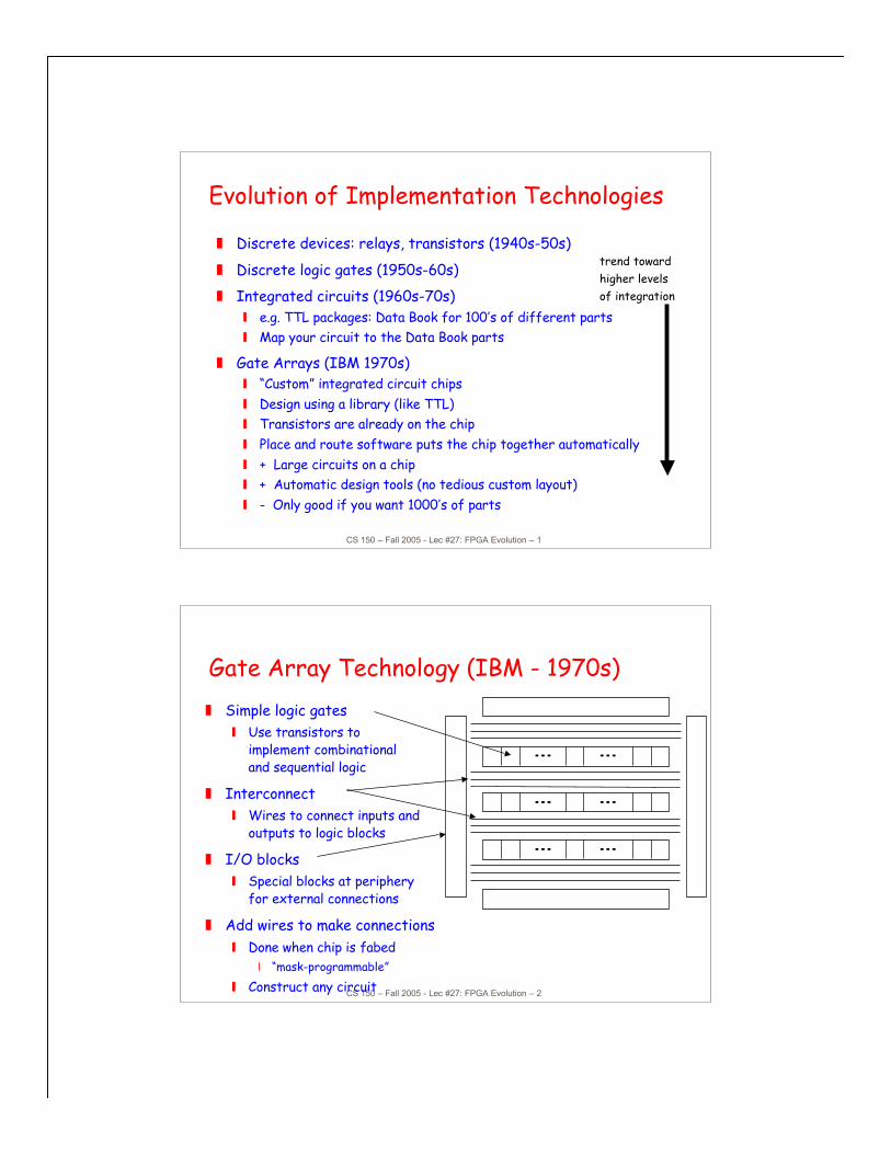
Evolution of Implementation Technologies
Discrete devices: relays, transistors (1940s-50s)
Discrete logic gates (1950s-60s)
Integrated circuits (1960s-70s) e.g. TTL packages: Data Book for 100’s of different parts Map your circuit to the Data Book parts
Gate Arrays (IBM 1970s) “Custom” integrated circuit chips Design using a library (like TTL) Transistors are already on the chip Place and route software puts the chip together automatically + Large circuits on a chip + Automatic design tools (no tedious custom layout) - Only good if you want 1000’s of parts
CS 150 – Fall 2005 - Lec #27: FPGA Evolution – 2
Gate Array Technology (IBM - 1970s) Simple logic gates
Use transistors toimplement combinationaland sequential logic
Interconnect Wires to connect inputs and
outputs to logic blocks
I/O blocks Special blocks at periphery
for external connections
Add wires to make connections Done when chip is fabed
“mask-programmable”
Construct any circuit
CS 150 – Fall 2005 - Lec #27: FPGA Evolution – 3
Programmable Logic
Disadvantages of the Data Book method Constrained to parts in the Data Book Parts are necessarily small and standard Need to stock many different parts
Programmable logic Use a single chip (or a small number of chips) Program it for the circuit you want No reason for the circuit to be small
CS 150 – Fall 2005 - Lec #27: FPGA Evolution – 4
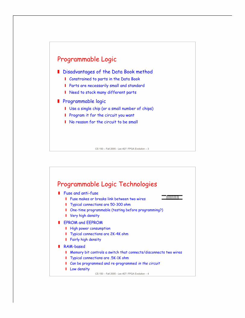
Programmable Logic Technologies Fuse and anti-fuse
Fuse makes or breaks link between two wires Typical connections are 50-300 ohm One-time programmable (testing before programming?) Very high density
EPROM and EEPROM High power consumption Typical connections are 2K-4K ohm Fairly high density
RAM-based Memory bit controls a switch that connects/disconnects two wires Typical connections are .5K-1K ohm Can be programmed and re-programmed in the circuit Low density
CS 150 – Fall 2005 - Lec #27: FPGA Evolution – 5
Programmable Logic Program a connection
Connect two wires Set a bit to 0 or 1
Regular structures for two-level logic (1960s-70s) All rely on two-level logic minimization PROM connections - permanent EPROM connections - erase with UV light EEPROM connections - erase electrically PROMs
Program connections in the _____________ plane PLAs
Program the connections in the ____________ plane PALs
Program the connections in the ____________ plane
CS 150 – Fall 2005 - Lec #27: FPGA Evolution – 6
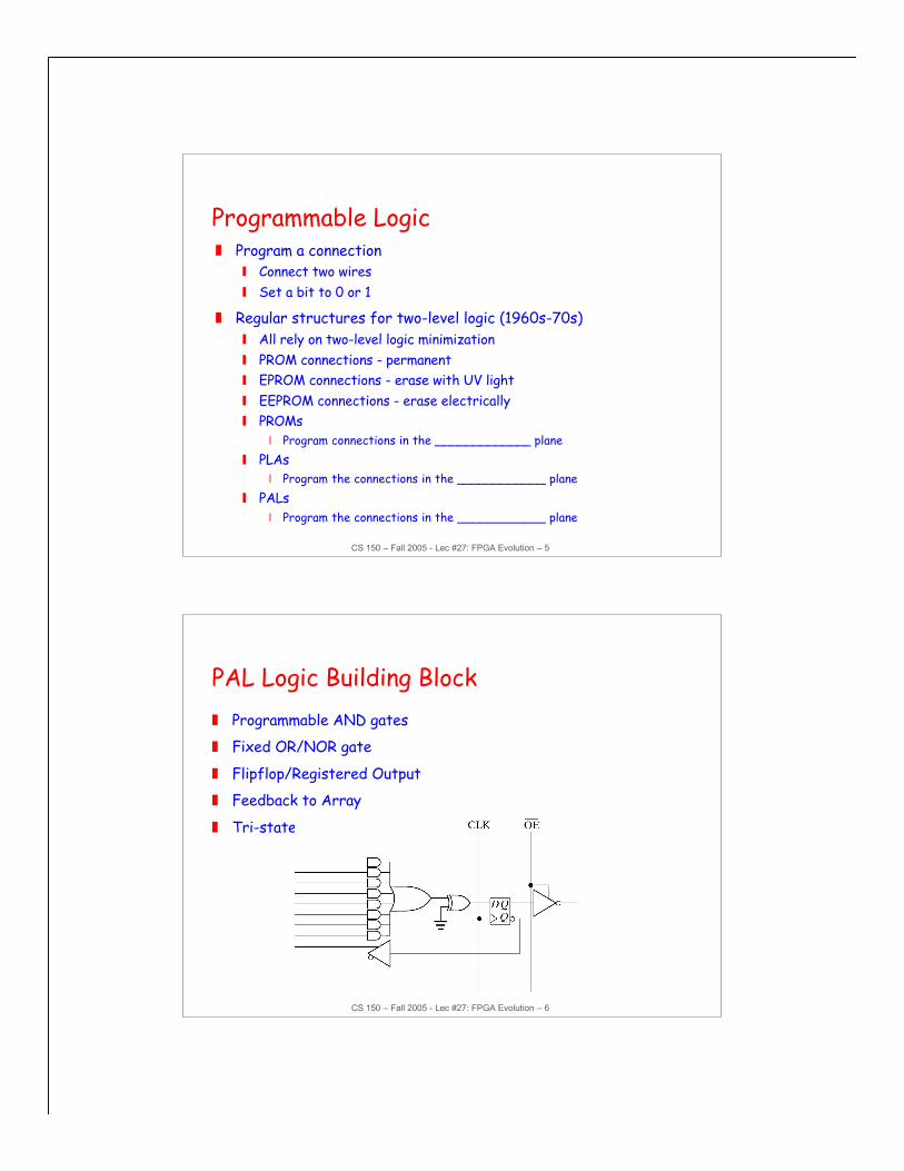
PAL Logic Building Block Programmable AND gates
Fixed OR/NOR gate
Flipflop/Registered Output
Feedback to Array
Tri-state Output
CS 150 – Fall 2005 - Lec #27: FPGA Evolution – 7
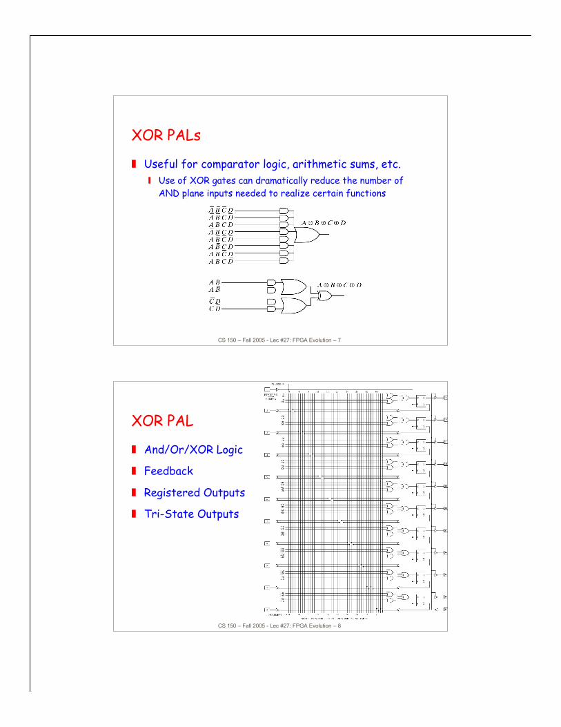
XOR PALs
Useful for comparator logic, arithmetic sums, etc. Use of XOR gates can dramatically reduce the number of
AND plane inputs needed to realize certain functions
CS 150 – Fall 2005 - Lec #27: FPGA Evolution – 8
XOR PAL
And/Or/XOR Logic
Feedback
Registered Outputs
Tri-State Outputs
CS 150 – Fall 2005 - Lec #27: FPGA Evolution – 9
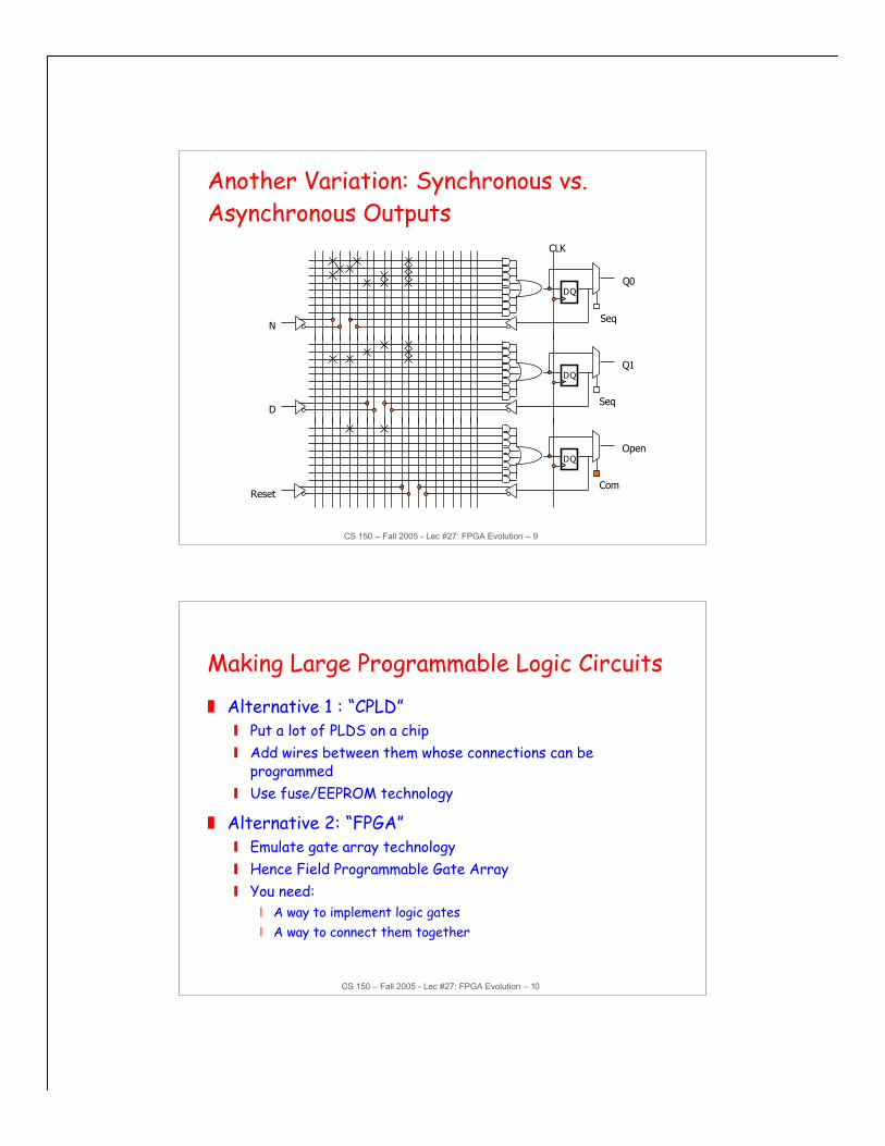
Another Variation: Synchronous vs.Asynchronous Outputs
DQ
DQ
DQ
Q0
Q1
Open
Com
Seq
Seq
CLK
N
D
Reset
CS 150 – Fall 2005 - Lec #27: FPGA Evolution – 10
Making Large Programmable Logic Circuits
Alternative 1 : “CPLD” Put a lot of PLDS on a chip Add wires between them whose connections can be
programmed Use fuse/EEPROM technology
Alternative 2: “FPGA” Emulate gate array technology Hence Field Programmable Gate Array You need:
A way to implement logic gates A way to connect them together
CS 150 – Fall 2005 - Lec #27: FPGA Evolution – 11
Field-Programmable Gate Arrays
PALs, PLAs = 10s – 100s Gate Equivalents
Field Programmable Gate Arrays = FPGAs Altera MAX Family Actel Programmable Gate Array Xilinx Logical Cell Array
1000s - 100000(s) of Gate Equivalents!
CS 150 – Fall 2005 - Lec #27: FPGA Evolution – 12
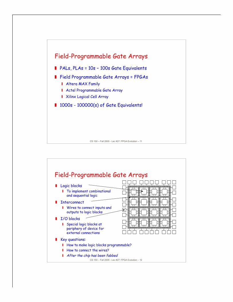
Field-Programmable Gate Arrays Logic blocks
To implement combinationaland sequential logic
Interconnect Wires to connect inputs and
outputs to logic blocks
I/O blocks Special logic blocks at
periphery of device forexternal connections
Key questions: How to make logic blocks programmable? How to connect the wires? After the chip has been fabbed
CS 150 – Fall 2005 - Lec #27: FPGA Evolution – 13
Tradeoffs in FPGAs Logic block - how are functions implemented: fixed functions
(manipulate inputs) or programmable? Support complex functions, need fewer blocks, but they are bigger
so less of them on chip Support simple functions, need more blocks, but they are smaller so
more of them on chip
Interconnect How are logic blocks arranged? How many wires will be needed between them? Are wires evenly distributed across chip? Programmability slows wires down – are some wires specialized to
long distances? How many inputs/outputs must be routed to/from each logic block? What utilization are we willing to accept? 50%? 20%? 90%?
CS 150 – Fall 2005 - Lec #27: FPGA Evolution – 14
Clk MUX
Output MUXQ
F/B MUX
Invert Control
AND ARRAY
CLK
pad
8 Product TermAND-OR Array
+Programmable
MUX's
Programmable polarity
I/O Pin
Seq. LogicBlock
Programmable feedback
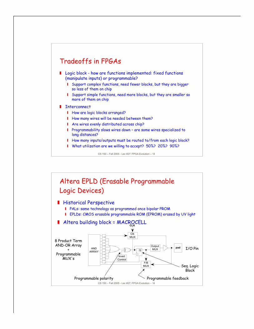
Altera EPLD (Erasable ProgrammableLogic Devices) Historical Perspective
PALs: same technology as programmed once bipolar PROM EPLDs: CMOS erasable programmable ROM (EPROM) erased by UV light
Altera building block = MACROCELL
CS 150 – Fall 2005 - Lec #27: FPGA Evolution – 15
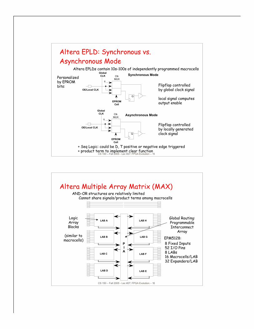
Altera EPLDs contain 10s-100s of independently programmed macrocells
Personalizedby EPROMbits: Flipflop controlled
by global clock signal
local signal computesoutput enable
Flipflop controlledby locally generatedclock signal
+ Seq Logic: could be D, T positive or negative edge triggered+ product term to implement clear function
Synchronous Mode
Asynchronous Mode
Global CLK
OE/Local CLK
EPROM Cell
1
Global CLK
OE/Local CLK
EPROM Cell
1
Clk MUX
Clk MUX
Q
Q
Altera EPLD: Synchronous vs.Asynchronous Mode
CS 150 – Fall 2005 - Lec #27: FPGA Evolution – 16
LAB A LAB H
LAB B LAB G
LAB C LAB F
LAB D LAB E
P I A
AND-OR structures are relatively limited Cannot share signals/product terms among macrocells
LogicArrayBlocks
(similar tomacrocells)
Global Routing:ProgrammableInterconnect
Array
8 Fixed Inputs52 I/O Pins8 LABs16 Macrocells/LAB32 Expanders/LAB
EPM5128:
Altera Multiple Array Matrix (MAX)
CS 150 – Fall 2005 - Lec #27: FPGA Evolution – 17
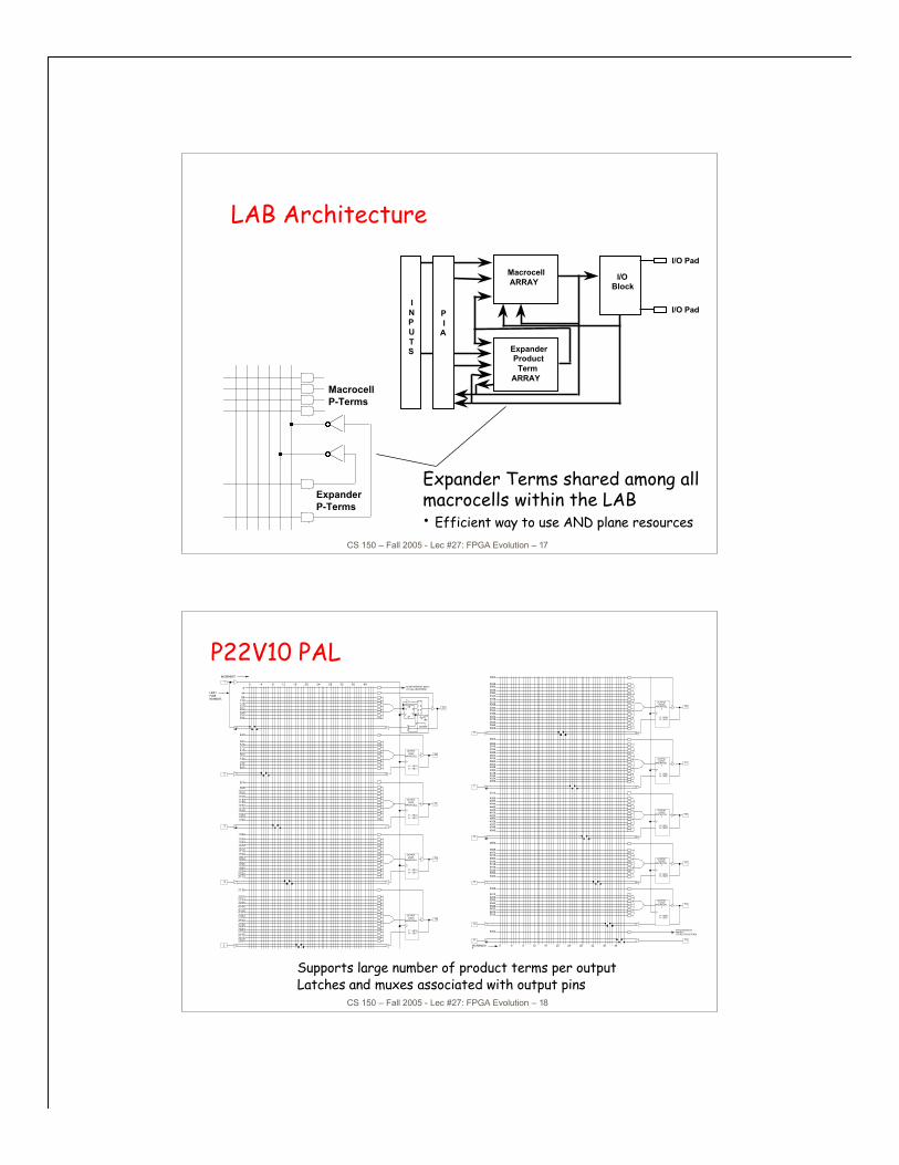
LAB Architecture
Expander Terms shared among allmacrocells within the LAB• Efficient way to use AND plane resources
Macrocell ARRAY I/O
Block
Expander Product
Term ARRAY
I NPUTS
P I
A
I/O Pad
I/O Pad
Macrocell P-Terms
Expander P-Terms
CS 150 – Fall 2005 - Lec #27: FPGA Evolution – 18
0 ASYNCHRONOUS RESET (TO ALL REGISTERS)
23AR
88132176220264308352396
44
22
2
OUTPUT LOGIC
MACROCELL
P - 5810 R - 5811
528572616660704748792836
484
880
440
21
3
OUTPUT LOGIC
MACROCELL
P - 5812 R - 5813
10561100114411881232127613201364
1012
1408
924
968
1452
20
4
OUTPUT LOGIC
MACROCELL
P - 5814 R - 5815
16721716176018041848189219361980
1628
2024
1496
1584
2068
1540
2112
19
5
OUTPUT LOGIC
MACROCELL
P - 5816 R - 5817
23762420246425082552259626402684
2332
2728
2156
2288
2772
22442200
28162860
1
1
00
1
0
01
D Q
QSP
10
5808P
R5809
10 4 8 12 16 20 24 28 32 36 40
INCREMENT
FIRST FUSE NUMBERS
15
9
OUTPUT LOGIC
MACROCELL
P - 5824 R - 5825
49725016506051045148519252365280
4928
5324
4884
17
7
OUTPUT LOGIC
MACROCELL
P - 5820 R - 5821
38283872391639604004404840924136
3784
4180
3652
3740
4224
3696
4268
16
8
OUTPUT LOGIC
MACROCELL
P - 5822 R - 5823
44444488453245764620466447084752
4400
4796
4312
4356
4840
18
6
OUTPUT LOGIC
MACROCELL
P - 5818 R - 5819
31243168321232563300334433883432
3080
3476
2904
3036
3520
29922948
35643608
14
10
OUTPUT LOGIC
MACROCELL
P - 5826 R - 5827
54125456550055445588563256765720
5368
11
5764
13
SYNCHRONOUS PRESET (TO ALL REGISTERS)
0 4 8 12 16 20 24 28 32 36 40INCREMENT
Supports large number of product terms per outputLatches and muxes associated with output pins
P22V10 PAL
CS 150 – Fall 2005 - Lec #27: FPGA Evolution – 19
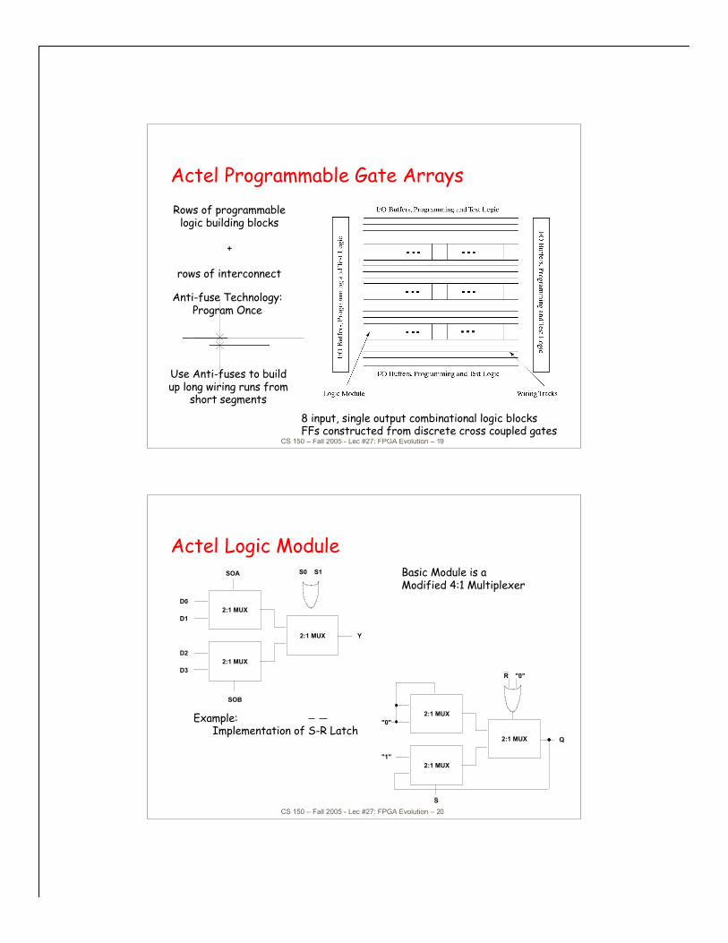
Rows of programmablelogic building blocks
+
rows of interconnect
Anti-fuse Technology:Program Once
8 input, single output combinational logic blocksFFs constructed from discrete cross coupled gates
Use Anti-fuses to buildup long wiring runs from
short segments
Actel Programmable Gate Arrays
CS 150 – Fall 2005 - Lec #27: FPGA Evolution – 20
Basic Module is aModified 4:1 Multiplexer
Example: Implementation of S-R Latch
2:1 MUXD0
D1
SOA
2:1 MUXD2
D3
SOB
2:1 MUX
S0
Y
S1
2:1 MUX"0"
R
2:1 MUX"1"
S
2:1 MUX Q
"0"
Actel Logic Module
CS 150 – Fall 2005 - Lec #27: FPGA Evolution – 21
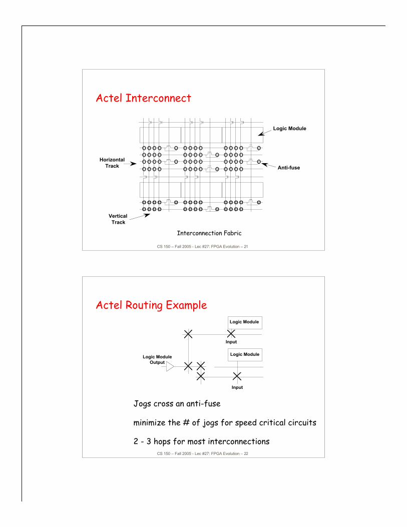
Interconnection Fabric
Logic Module
Horizontal Track
Vertical Track
Anti-fuse
Actel Interconnect
CS 150 – Fall 2005 - Lec #27: FPGA Evolution – 22
Jogs cross an anti-fuse
minimize the # of jogs for speed critical circuits
2 - 3 hops for most interconnections
Logic Module
Logic ModuleLogic Module Output
Input
Input
Actel Routing Example
CS 150 – Fall 2005 - Lec #27: FPGA Evolution – 23
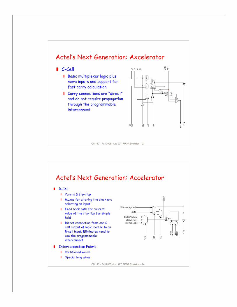
Actel’s Next Generation: Axcelerator
C-Cell Basic multiplexer logic plus
more inputs and support forfast carry calculation
Carry connections are “direct”and do not require propagationthrough the programmableinterconnect
CS 150 – Fall 2005 - Lec #27: FPGA Evolution – 24
Actel’s Next Generation: Accelerator R-Cell
Core is D flip-flop Muxes for altering the clock and
selecting an input Feed back path for current
value of the flip-flop for simplehold
Direct connection from one C-cell output of logic module to anR-cell input; Eliminates need touse the programmableinterconnect
Interconnection Fabric Partitioned wires Special long wires
CS 150 – Fall 2005 - Lec #27: FPGA Evolution – 25
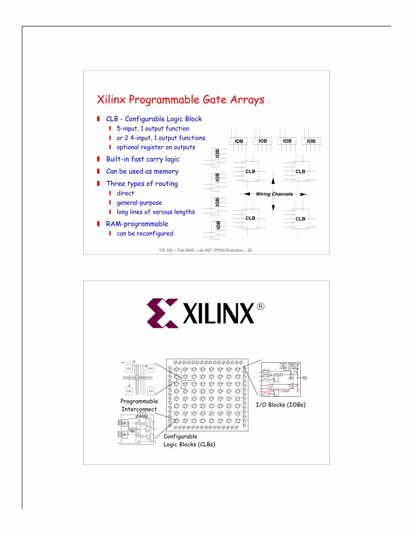
IOB IOB IOB IOB
CLB CLB
CLB CLBIO
BIO
BIO
BIO
B
Wiring Channels
Xilinx Programmable Gate Arrays CLB - Configurable Logic Block
5-input, 1 output function or 2 4-input, 1 output functions optional register on outputs
Built-in fast carry logic
Can be used as memory
Three types of routing direct general-purpose long lines of various lengths
RAM-programmable can be reconfigured
CLB
CLB
CLB
CLB
SwitchMatrix
ProgrammableInterconnect
I/O Blocks (IOBs)
ConfigurableLogic Blocks (CLBs)
D Q
SlewRate
Control
PassivePull-Up,
Pull-Down
Delay
Vcc
OutputBuffer
InputBuffer
Q D
Pad
D QSD
RDEC
S/RControl
D QSD
RDEC
S/RControl
1
1
F'G'
H'
DIN
F'G'
H'
DIN
F'
G'H'
H'
HFunc.Gen.
GFunc.Gen.
FFunc.Gen.
G4G3G2G1
F4F3F2F1
C4C1 C2 C3
K
Y
X
H1 DIN S/R EC
CS 150 – Fall 2005 - Lec #27: FPGA Evolution – 27
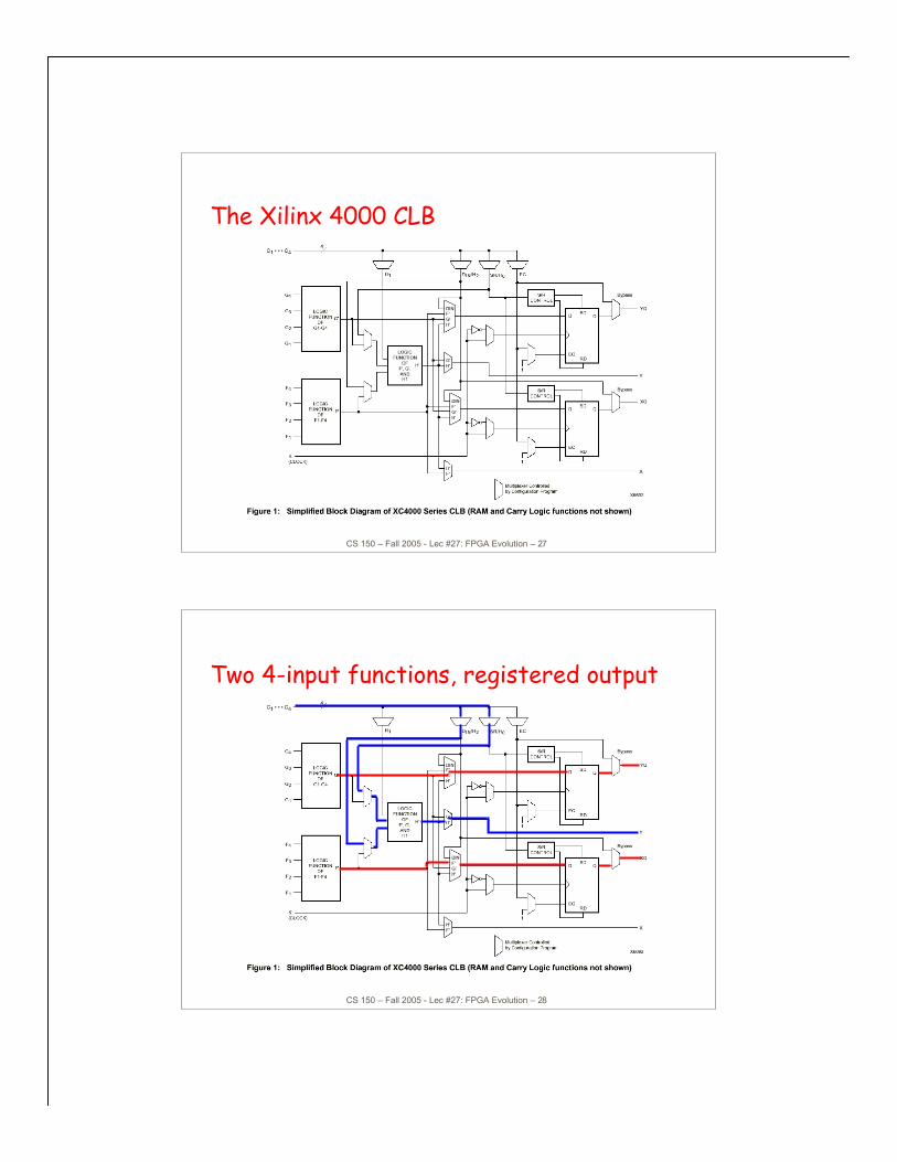
The Xilinx 4000 CLB
CS 150 – Fall 2005 - Lec #27: FPGA Evolution – 28
Two 4-input functions, registered output
CS 150 – Fall 2005 - Lec #27: FPGA Evolution – 29
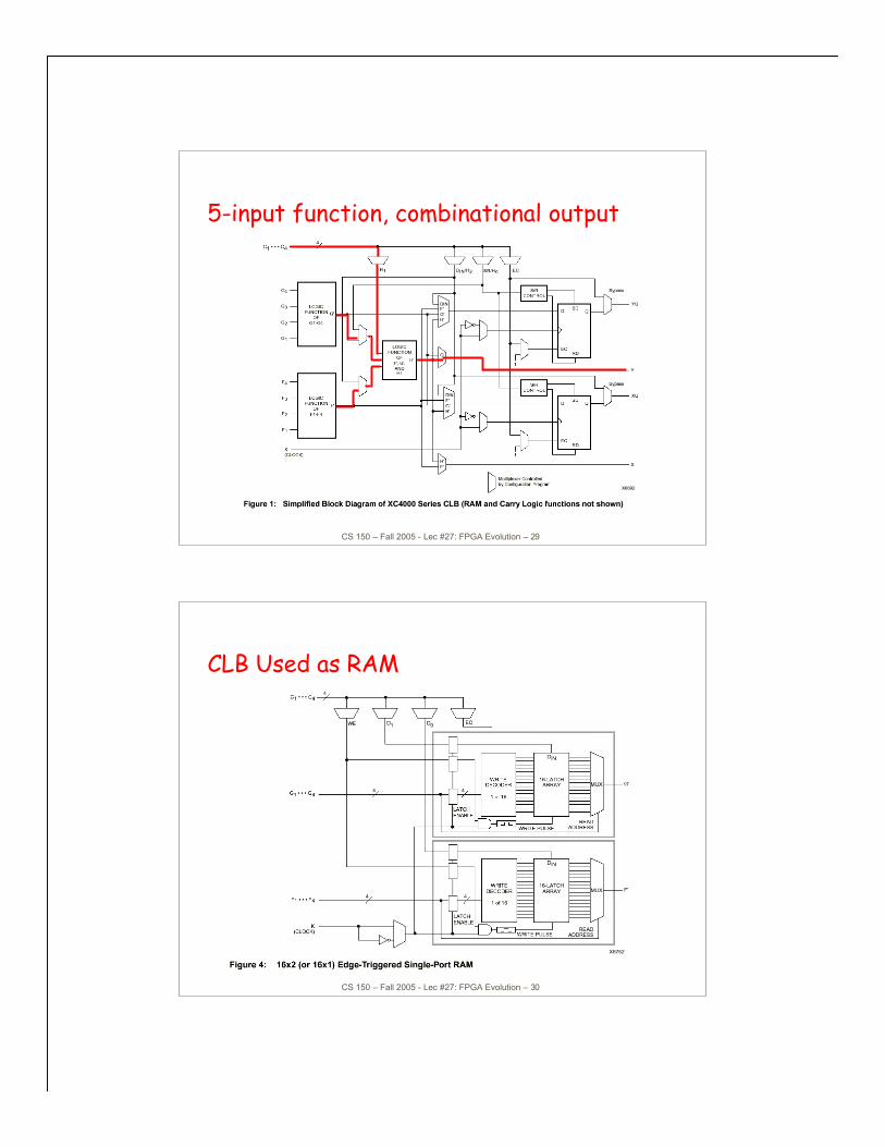
5-input function, combinational output
CS 150 – Fall 2005 - Lec #27: FPGA Evolution – 30
CLB Used as RAM
CS 150 – Fall 2005 - Lec #27: FPGA Evolution – 31
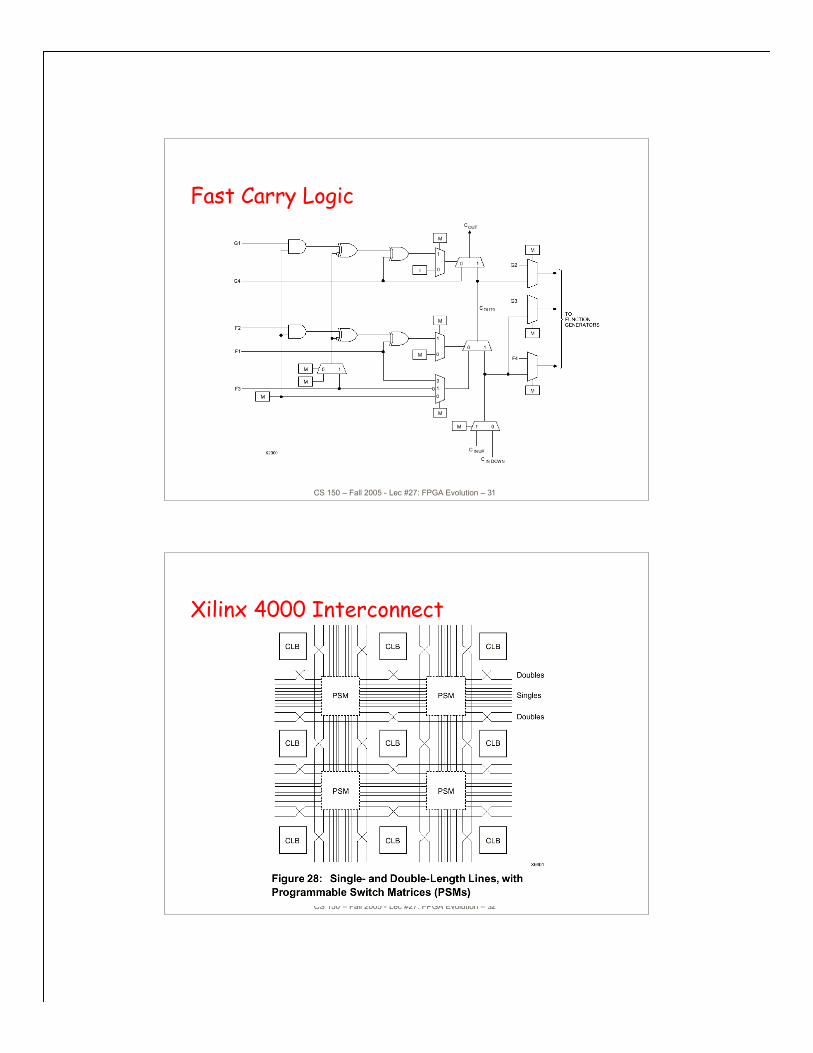
Fast Carry Logic
CS 150 – Fall 2005 - Lec #27: FPGA Evolution – 32
Xilinx 4000 Interconnect
CS 150 – Fall 2005 - Lec #27: FPGA Evolution – 33
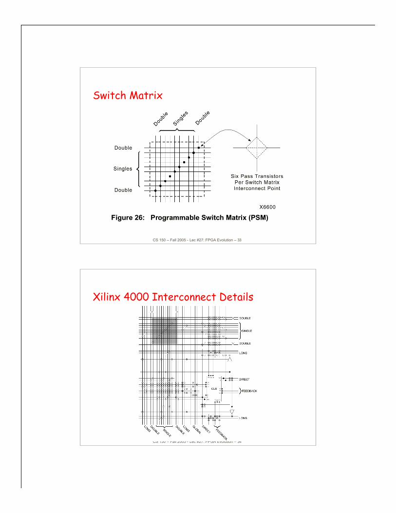
Switch Matrix
CS 150 – Fall 2005 - Lec #27: FPGA Evolution – 34
Xilinx 4000 Interconnect Details
CS 150 – Fall 2005 - Lec #27: FPGA Evolution – 35
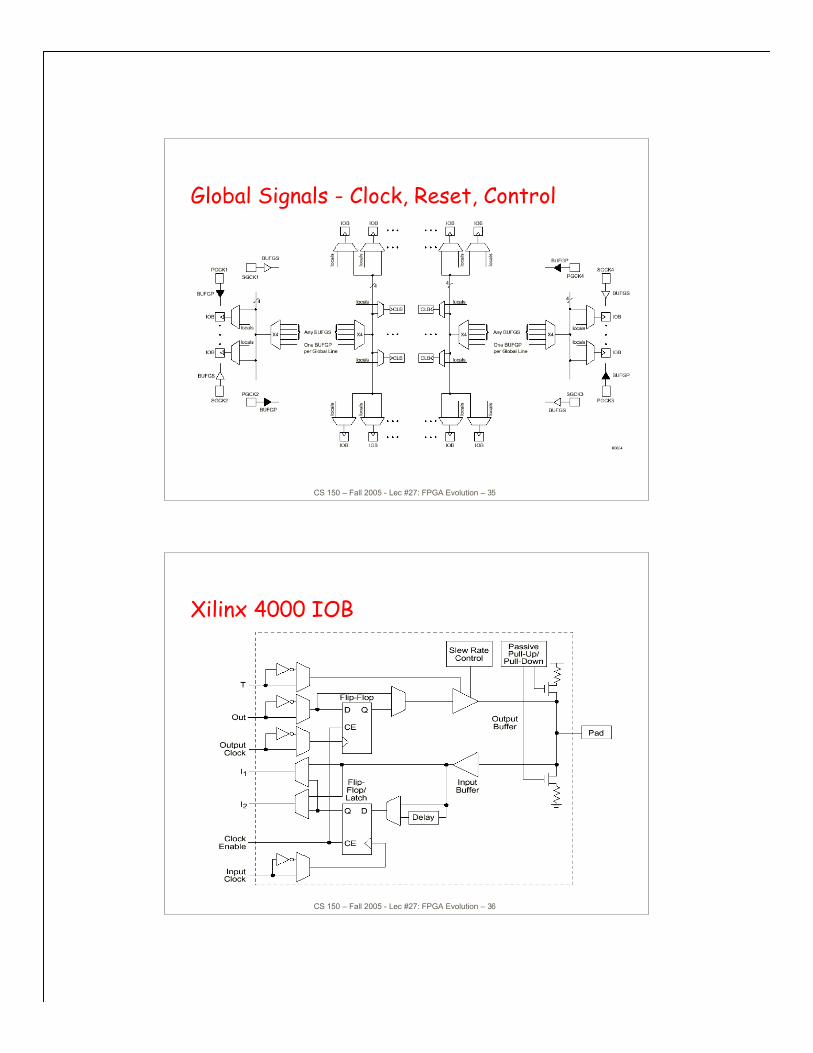
Global Signals - Clock, Reset, Control
CS 150 – Fall 2005 - Lec #27: FPGA Evolution – 36
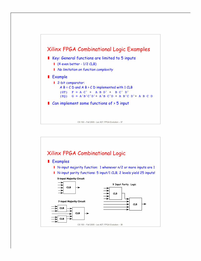
Xilinx 4000 IOB
CS 150 – Fall 2005 - Lec #27: FPGA Evolution – 37
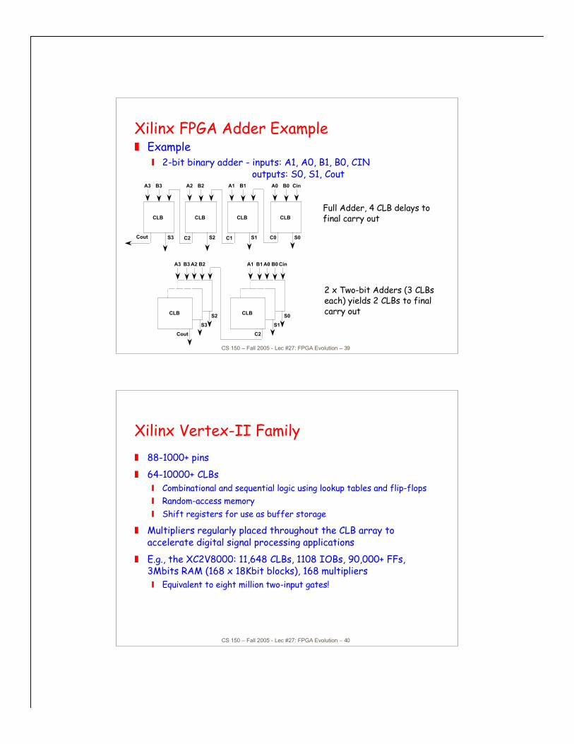
Xilinx FPGA Combinational Logic Examples Key: General functions are limited to 5 inputs
(4 even better - 1/2 CLB) No limitation on function complexity
Example 2-bit comparator:
A B = C D and A B > C D implemented with 1 CLB(GT) F = A C' + A B D' + B C' D'(EQ) G = A'B'C'D'+ A'B C'D + A B'C D'+ A B C D
Can implement some functions of > 5 input
CS 150 – Fall 2005 - Lec #27: FPGA Evolution – 38
CLB
5-input Majority Circuit
CLB
CLB
CLB
7-input Majority Circuit
Xilinx FPGA Combinational Logic Examples
N-input majority function: 1 whenever n/2 or more inputs are 1 N-input parity functions: 5 input/1 CLB; 2 levels yield 25 inputs!
CLB
CLB
9 Input Parity Logic
CS 150 – Fall 2005 - Lec #27: FPGA Evolution – 39
Xilinx FPGA Adder Example Example
2-bit binary adder - inputs: A1, A0, B1, B0, CIN outputs: S0, S1, Cout
CLB
A0 B0 Cin
S0
CLB
A1 B1
S1
CLB
A2 B2
C1S2
CLB
A3 B3
C2S3 C0Cout
S0
S1
C2
A1 B1 CinA0 B0
CLBS2
S3
Cout
A3 B3A2 B2
CLB
Full Adder, 4 CLB delays tofinal carry out
2 x Two-bit Adders (3 CLBseach) yields 2 CLBs to finalcarry out
CS 150 – Fall 2005 - Lec #27: FPGA Evolution – 40
Xilinx Vertex-II Family 88-1000+ pins
64-10000+ CLBs Combinational and sequential logic using lookup tables and flip-flops Random-access memory Shift registers for use as buffer storage
Multipliers regularly placed throughout the CLB array toaccelerate digital signal processing applications
E.g., the XC2V8000: 11,648 CLBs, 1108 IOBs, 90,000+ FFs,3Mbits RAM (168 x 18Kbit blocks), 168 multipliers Equivalent to eight million two-input gates!
CS 150 – Fall 2005 - Lec #27: FPGA Evolution – 41
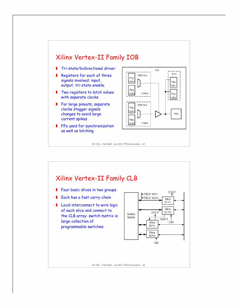
Xilinx Vertex-II Family IOB Tri-state/bidirectional driver
Registers for each of threesignals involved: input,output, tri-state enable.
Two registers to latch valueswith separate clocks.
For large pinouts, separateclocks stagger signalschanges to avoid largecurrent spikes
FFs used for synchronizationas well as latching
CS 150 – Fall 2005 - Lec #27: FPGA Evolution – 42
Xilinx Vertex-II Family CLB Four basic slices in two groups
Each has a fast carry-chain
Local interconnect to wire logicof each slice and connect tothe CLB array: switch matrix islarge collection ofprogrammable switches
CS 150 – Fall 2005 - Lec #27: FPGA Evolution – 43
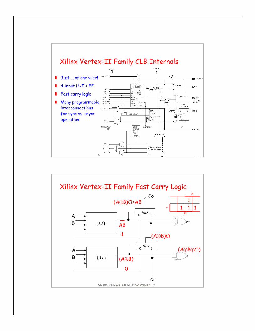
Xilinx Vertex-II Family CLB Internals
Just _ of one slice!
4-input LUT + FF
Fast carry logic
Many programmableinterconnectionsfor sync vs. asyncoperation
CS 150 – Fall 2005 - Lec #27: FPGA Evolution – 44
Xilinx Vertex-II Family Fast Carry Logic
LUT
LUT
AB
AB
Mux0 1
Mux0 1
Ci
Co
0
(A⊕B)Ci
(A⊕B)
(A⊕B⊕Ci)
(A⊕B)Ci+AB
AB
1
A
C
B
111 1
CS 150 – Fall 2005 - Lec #27: FPGA Evolution – 45
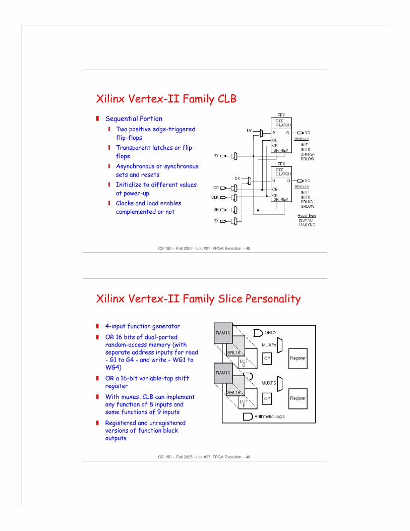
Xilinx Vertex-II Family CLB Sequential Portion
Two positive edge-triggeredflip-flops
Transparent latches or flip-flops
Asynchronous or synchronoussets and resets
Initialize to different valuesat power-up
Clocks and load enablescomplemented or not
CS 150 – Fall 2005 - Lec #27: FPGA Evolution – 46
Xilinx Vertex-II Family Slice Personality
4-input function generator
OR 16 bits of dual-portedrandom-access memory (withseparate address inputs for read- G1 to G4 - and write - WG1 toWG4)
OR a 16-bit variable-tap shiftregister
With muxes, CLB can implementany function of 8 inputs andsome functions of 9 inputs
Registered and unregisteredversions of function blockoutputs
CS 150 – Fall 2005 - Lec #27: FPGA Evolution – 47
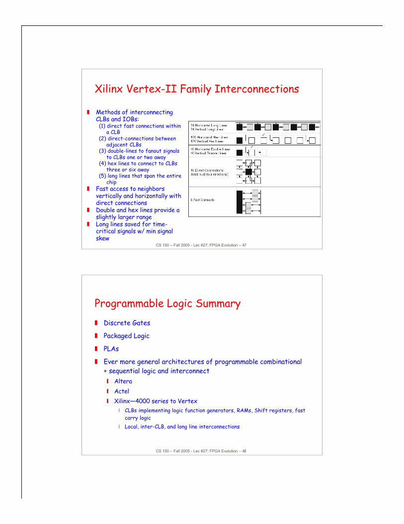
Xilinx Vertex-II Family Interconnections
Methods of interconnectingCLBs and IOBs:(1) direct fast connections within
a CLB(2) direct-connections between
adjacent CLBs(3) double-lines to fanout signals
to CLBs one or two away(4) hex lines to connect to CLBs
three or six away(5) long lines that span the entire
chip Fast access to neighbors
vertically and horizontally withdirect connections
Double and hex lines provide aslightly larger range
Long lines saved for time-critical signals w/ min signalskew
CS 150 – Fall 2005 - Lec #27: FPGA Evolution – 48
Programmable Logic Summary Discrete Gates
Packaged Logic
PLAs
Ever more general architectures of programmable combinational+ sequential logic and interconnect Altera Actel Xilinx—4000 series to Vertex
CLBs implementing logic function generators, RAMs, Shift registers, fastcarry logic
Local, inter-CLB, and long line interconnections