Embed Size (px)
Citation preview
55:041 Electronic Circuits The University of Iowa Fall 2011
1
Exam 2
Name: ___________________________ Score__________/90___
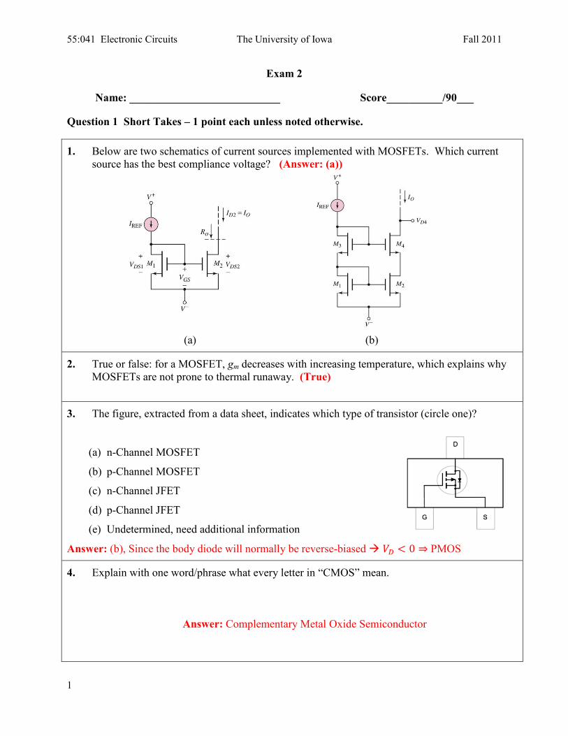
Question 1 Short Takes – 1 point each unless noted otherwise.
1. Below are two schematics of current sources implemented with MOSFETs. Which current
source has the best compliance voltage? (Answer: (a))
(a) (b)
2. True or false: for a MOSFET, gm decreases with increasing temperature, which explains why
MOSFETs are not prone to thermal runaway. (True)
3. The figure, extracted from a data sheet, indicates which type of transistor (circle one)?
(a) n-Channel MOSFET
(b) p-Channel MOSFET
(c) n-Channel JFET
(d) p-Channel JFET
(e) Undetermined, need additional information
Answer: (b), Since the body diode will normally be reverse-biased PMOS
4. Explain with one word/phrase what every letter in “CMOS” mean.
Answer: Complementary Metal Oxide Semiconductor
55:041 Electronic Circuits The University of Iowa Fall 2011
2
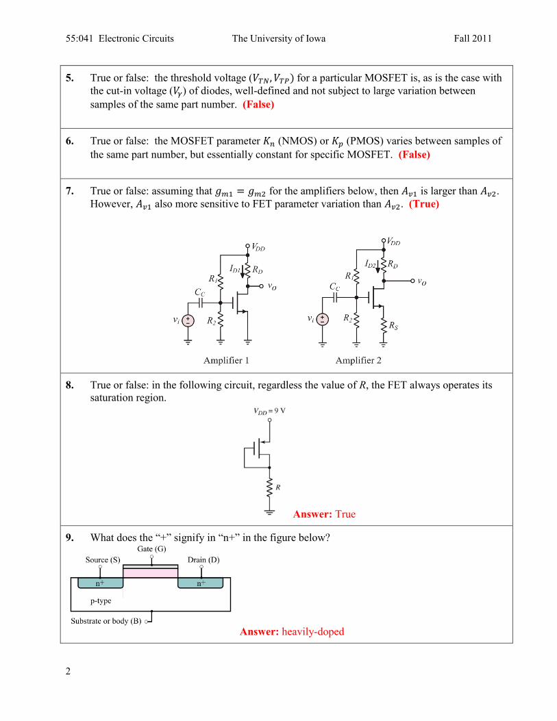
5. True or false: the threshold voltage ( for a particular MOSFET is, as is the case with
the cut-in voltage ( ) of diodes, well-defined and not subject to large variation between
samples of the same part number. (False)
6. True or false: the MOSFET parameter (NMOS) or (PMOS) varies between samples of
the same part number, but essentially constant for specific MOSFET. (False)
7. True or false: assuming that for the amplifiers below, then is larger than .
However, also more sensitive to FET parameter variation than . (True)
8. True or false: in the following circuit, regardless the value of R, the FET always operates its
saturation region.
Answer: True
9. What does the “+” signify in “n+” in the figure below?
Answer: heavily-doped
55:041 Electronic Circuits The University of Iowa Fall 2011
3
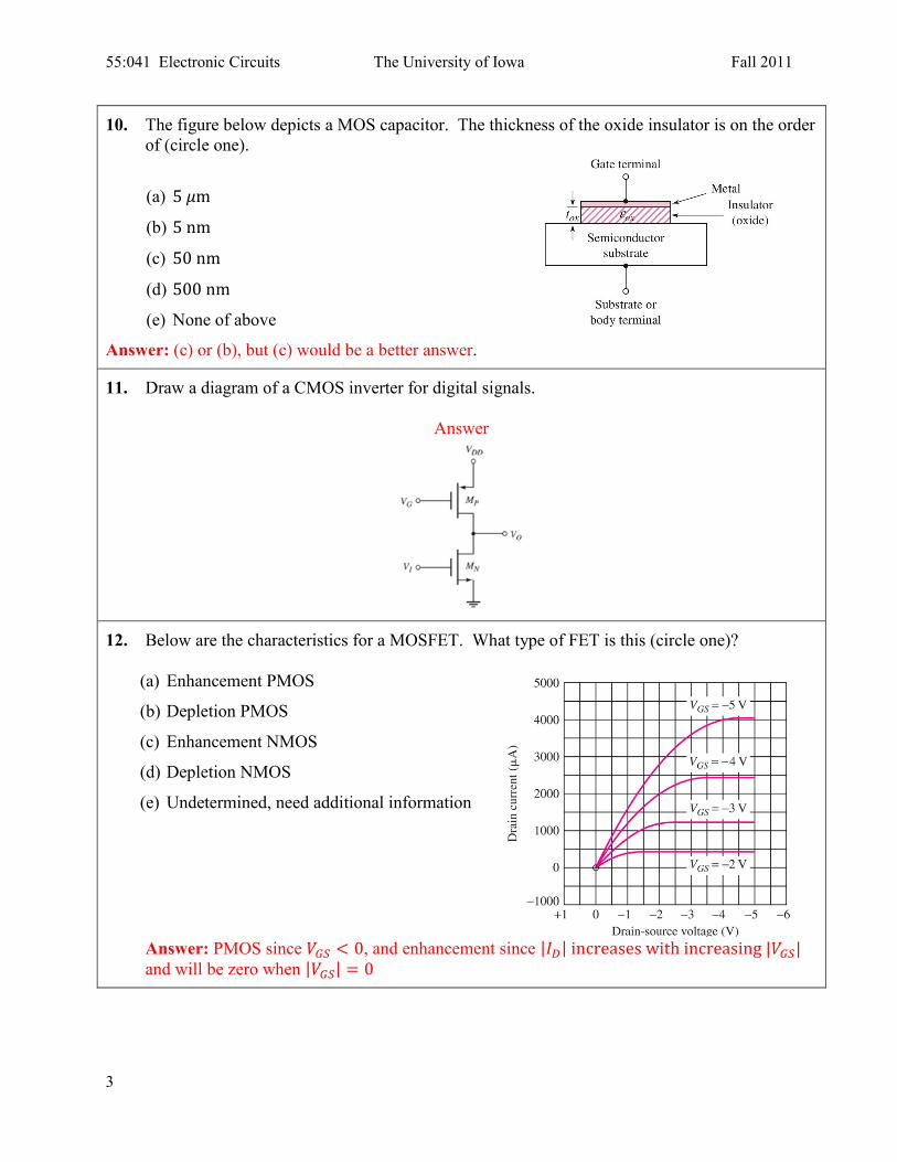
10. The figure below depicts a MOS capacitor. The thickness of the oxide insulator is on the order
of (circle one).
(a)
(b)
(c)
(d)
(e) None of above
Answer: (c) or (b), but (c) would be a better answer.
11. Draw a diagram of a CMOS inverter for digital signals.
Answer
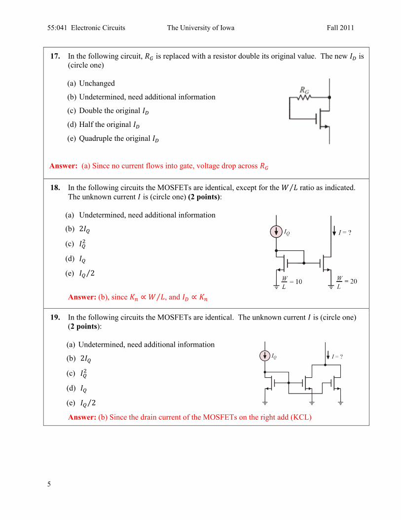
12. Below are the characteristics for a MOSFET. What type of FET is this (circle one)?
(a) Enhancement PMOS
(b) Depletion PMOS
(c) Enhancement NMOS
(d) Depletion NMOS
(e) Undetermined, need additional information
Answer: PMOS since , and enhancement since | | | | and will be zero when | |
55:041 Electronic Circuits The University of Iowa Fall 2011
4
13. Write down the dc load line equation for the MOSFET in the circuit below. (2 points)
14. Briefly explain (1–2 sentences) what is ( as it pertains to MOSFETs. (2 points)
Answer: This is parameter found in MOSFET data sheets and typically indicate the lowest
resistance between Drain and Source when the FET is turned on “hard” That is, when
(NMOS) or | | | | (PMOS)
15. True or false: given the symmetrical construction of MOSFETs one can, in principle, at least,
interchange the drain and the source terminals without affecting device behavior.
Answer: True
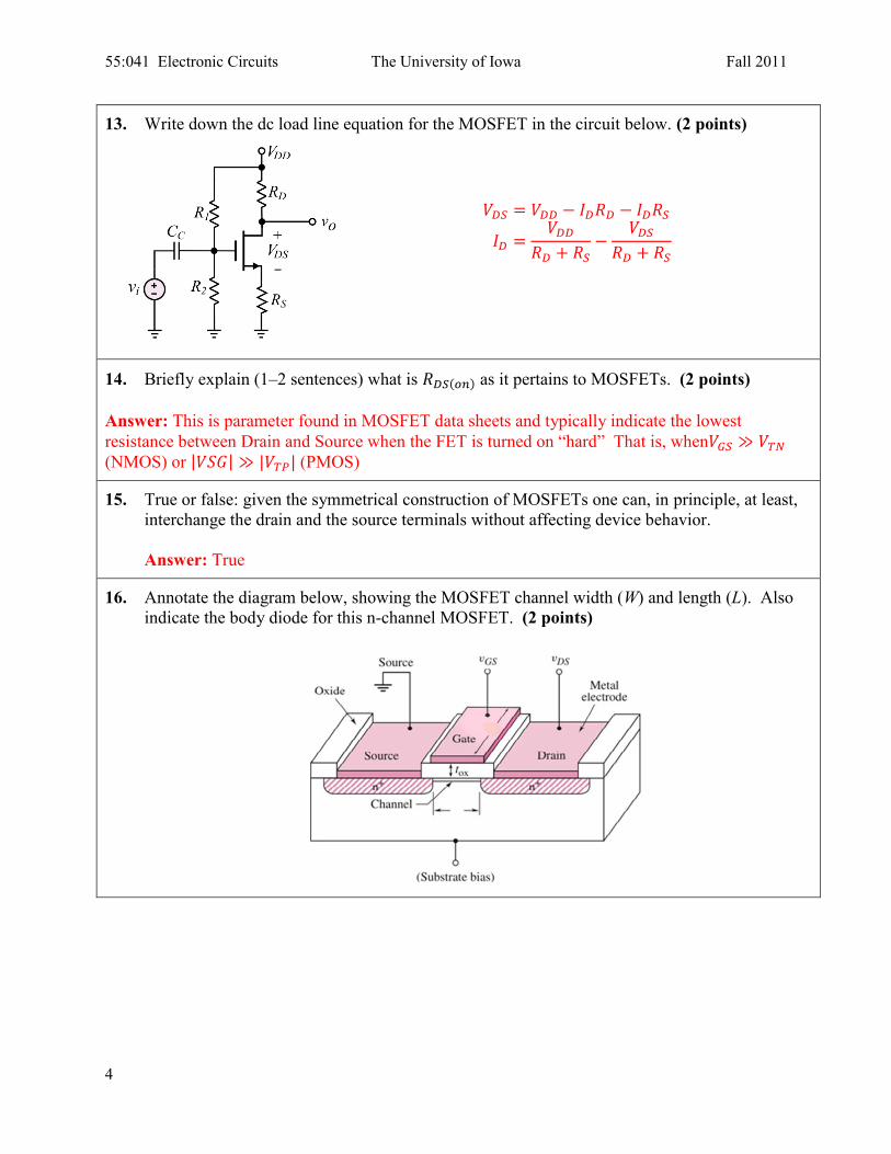
16. Annotate the diagram below, showing the MOSFET channel width (W) and length (L). Also
indicate the body diode for this n-channel MOSFET. (2 points)
55:041 Electronic Circuits The University of Iowa Fall 2011
5
17. In the following circuit, is replaced with a resistor double its original value. The new is
(circle one)
(a) Unchanged
(b) Undetermined, need additional information
(c) Double the original
(d) Half the original
(e) Quadruple the original
Answer: (a) Since no current flows into gate, voltage drop across
18. In the following circuits the MOSFETs are identical, except for the ⁄ ratio as indicated.
The unknown current is (circle one) (2 points):
(a) Undetermined, need additional information
(b)
(c)
(d)
(e) ⁄
Answer: (b), since ⁄ , and
19. In the following circuits the MOSFETs are identical. The unknown current is (circle one)
(2 points):
(a) Undetermined, need additional information
(b)
(c)
(d)
(e) ⁄
Answer: (b) Since the drain current of the MOSFETs on the right add (KCL)
55:041 Electronic Circuits The University of Iowa Fall 2011
6
20. A MOSFET is operating in saturation at and ⁄ . If
increases by 10 mV, the new is (circle one) (2 points):
(a) Unchanged, because the MOSFET is in saturation and behaves line like current source
(b) Undetermined, need additional information
(c)
(d)
(e) 2.0283 mA
Answer: (e) because the change in is ( ( and the
new Q-value is 3 mA.
55:041 Electronic Circuits The University of Iowa Fall 2011
7
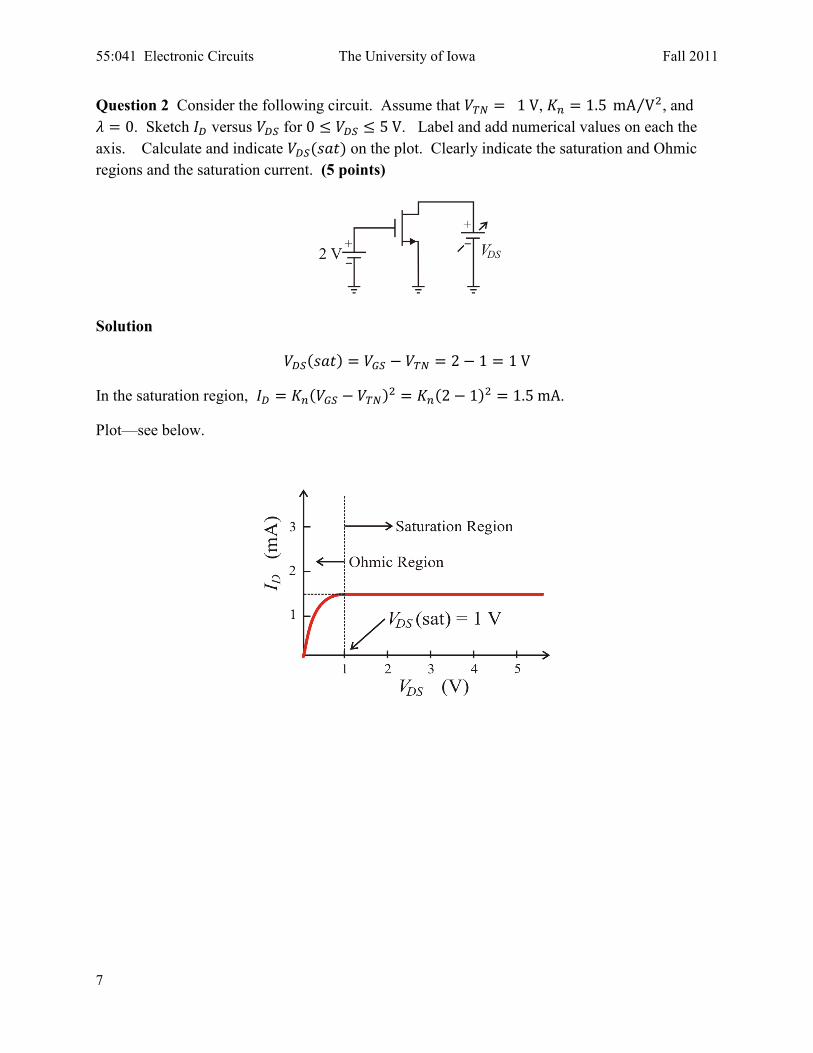
Question 2 Consider the following circuit. Assume that , ⁄ , and
. Sketch versus for . Label and add numerical values on each the
axis. Calculate and indicate ( on the plot. Clearly indicate the saturation and Ohmic
regions and the saturation current. (5 points)
Solution
(
In the saturation region, ( ( .
Plot—see below.
55:041 Electronic Circuits The University of Iowa Fall 2011
8
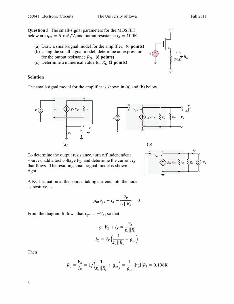
Question 3 The small-signal parameters for the MOSFET
below are ⁄ and output resistance .
(a) Draw a small-signal model for the amplifier. (6 points)
(b) Using the small-signal model, determine an expression
for the output resistance . (6 points)
(c) Determine a numerical value for (2 points)
Solution
The small-signal model for the amplifier is shown in (a) and (b) below.
(a) (b)
To determine the output resistance, turn off independent
sources, add a test voltage , and determine the current
that flows. The resulting small-signal model is shown
right.
A KCL equation at the source, taking currents into the node
as positive, is
||
From the diagram follows that , so that
||
(
|| )
Then
(
|| )
|| || ⁄
Ro
55:041 Electronic Circuits The University of Iowa Fall 2011
9
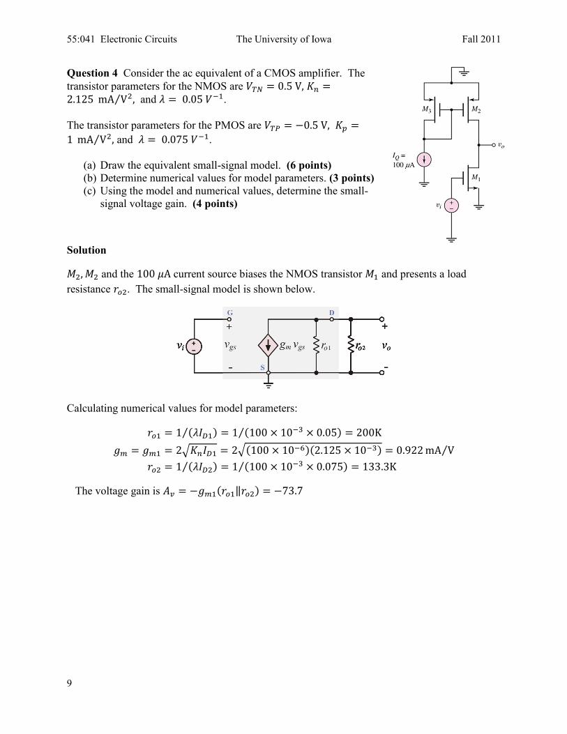
Question 4 Consider the ac equivalent of a CMOS amplifier. The
transistor parameters for the NMOS are ⁄ and .
The transistor parameters for the PMOS are
⁄ and .
(a) Draw the equivalent small-signal model. (6 points)
(b) Determine numerical values for model parameters. (3 points)
(c) Using the model and numerical values, determine the small-
signal voltage gain. (4 points)
Solution
and the current source biases the NMOS transistor and presents a load
resistance . The small-signal model is shown below.
Calculating numerical values for model parameters:
( ( ⁄⁄
√ √( ( ⁄
( ( ⁄⁄
The voltage gain is ( ‖
55:041 Electronic Circuits The University of Iowa Fall 2011
10
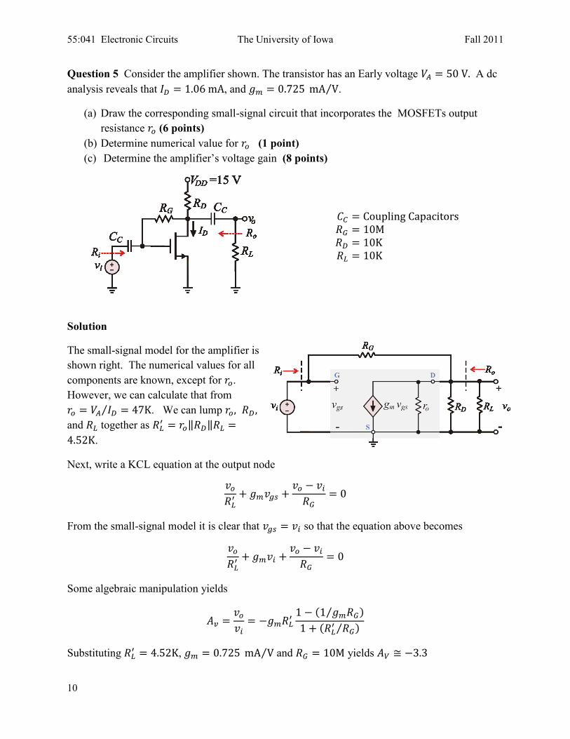
Question 5 Consider the amplifier shown. The transistor has an Early voltage A dc
analysis reveals that , and ⁄ .
(a) Draw the corresponding small-signal circuit that incorporates the MOSFETs output
resistance (6 points)
(b) Determine numerical value for (1 point)
(c) Determine the amplifier’s voltage gain (8 points)
Solution
The small-signal model for the amplifier is
shown right. The numerical values for all
components are known, except for .
However, we can calculate that from
⁄ . We can lump
and together as ‖ ‖
.
Next, write a KCL equation at the output node
From the small-signal model it is clear that so that the equation above becomes
Some algebraic manipulation yields
( ⁄
( ⁄
Substituting , ⁄ and yields

55:041 Electronic Circuits The University of Iowa Fall 2011
11
Page intentionally left blank
55:041 Electronic Circuits The University of Iowa Fall 2011
12
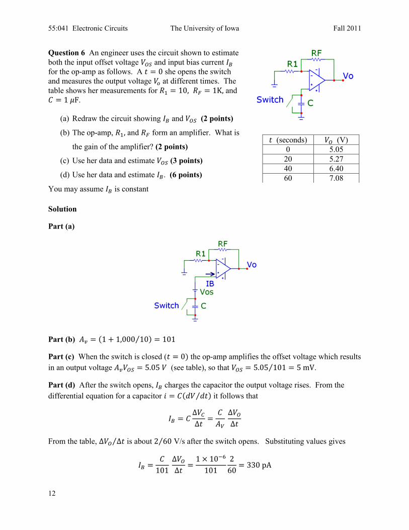
Question 6 An engineer uses the circuit shown to estimate
both the input offset voltage and input bias current
for the op-amp as follows. A she opens the switch
and measures the output voltage at different times. The
table shows her measurements for and
.
(a) Redraw the circuit showing and (2 points)
(b) The op-amp, and form an amplifier. What is
the gain of the amplifier? (2 points)
(c) Use her data and estimate (3 points)
(d) Use her data and estimate . (6 points)
You may assume is constant
(seconds) (V)
0 5.05
20 5.27
40 6.40
60 7.08
Solution
Part (a)
Part (b) ( ⁄
Part (c) When the switch is closed ( the op-amp amplifies the offset voltage which results
in an output voltage (see table), so that ⁄ .
Part (d) After the switch opens, charges the capacitor the output voltage rises. From the
differential equation for a capacitor ( ⁄ it follows that
From the table, ⁄ is about ⁄ V/s after the switch opens. Substituting values gives

55:041 Electronic Circuits The University of Iowa Fall 2011
13
Page Intentionally Left Blank
55:041 Electronic Circuits The University of Iowa Fall 2011
14
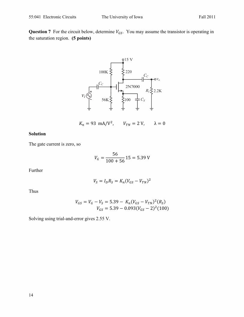
Question 7 For the circuit below, determine . You may assume the transistor is operating in
the saturation region. (5 points)
Solution
The gate current is zero, so
Further
(
Thus
( (
( (
Solving using trial-and-error gives 2.55 V.


![Day 1: Student takes exam in D2L with Software Secure ......Division of Continuing Studies [ONLINE EXAM PROCEDURE] The timeline from Exam to posted grade: Day 1: Student takes exam](https://img.pdfslide.net/doc/110x75/5f2c941102593f3954585ca6/day-1-student-takes-exam-in-d2l-with-software-secure-division-of-continuing.jpg)