Embed Size (px)
Citation preview

University of New MexicoUNM Digital Repository
Electrical and Computer Engineering ETDs Engineering ETDs
Spring 4-12-2018
Experimental Testing of a Metamaterial Slow WaveStructure for High-Power Microwave GenerationKevin Aaron ShipmanUniversity of New Mexico - Main Campus
Follow this and additional works at: https://digitalrepository.unm.edu/ece_etds
Part of the Electromagnetics and Photonics Commons
This Thesis is brought to you for free and open access by the Engineering ETDs at UNM Digital Repository. It has been accepted for inclusion inElectrical and Computer Engineering ETDs by an authorized administrator of UNM Digital Repository. For more information, please [email protected].
Recommended CitationShipman, Kevin Aaron. "Experimental Testing of a Metamaterial Slow Wave Structure for High-Power Microwave Generation."(2018). https://digitalrepository.unm.edu/ece_etds/401

i
Kevin Aaron Shipman Candidate
Electrical and Computer Engineering
Department
This thesis is approved, and it is acceptable in quality and form for publication:
Approved by the Thesis Committee:
Mark Gilmore, Chairperson
Edl Schamiloglu
Dustin Fisher
ii
EXPERMENTAL TESTING OF A METAMATERIAL SLOW
WAVE STRUCTURE FOR HIGH-POWER MICROWAVE
GENERATION
by
KEVIN AARON SHIPMAN
A.S., MATHEMATICS
B.S., EXERCISE SCIENCE
THESIS
Submitted in Partial Fulfillment of the
Requirements for the Degree of
Masters of Science
Electrical Engineering
The University of New Mexico
Albuquerque, New Mexico
May, 2018

iii
DEDICATION
I would like to dedicate this thesis to my parents, Robert and Susan Shipman, and my
grandfather, Robert Dungan. Thank you for always being there for me and supporting me
through life. None of this would be possible without you.

iv
ACKNOWLEDGMENTS
I would like to thank Professor Mark Gilmore for believing in me and giving me
this opportunity to pursue and complete this research. I would like to thank Professor Edl
Schamiloglu for allowing me to take over this research when it seemed like it was going to
be doomed. He allowed me to take over and run his lab and allowed me to have a tangible
thesis. I also want to thank Dr. Dustin Fisher, for all his help with the MATLAB coding
and helping develop a mode analysis technique that can hopefully be improved upon in the
future to become a valuable diagnostic in this field. I would also like to thank Dmitrii
Andreev and Daniel Reass for helping me setup and conduct experiments, I would not have
been able to do any of this without their help.
The research presented in this thesis was supported by AFOSR MURI Grant
FA9550-12-1-0489.
v
Experimental Testing of a Metamaterial Slow Wave Structure for High-
Power Microwave Generation
by
Kevin Aaron Shipman
B.S., Exercise Science, University of New Mexico, 2008
A.S., Mathematics, San Juan College, 2014
M.S., Electrical Engineering, University of New Mexico, 2018
Abstract
A high-power L-band microwave source has been developed using a metamaterial
(MTM) to produce a biperiodic double negative slow wave structure (SWS) for interaction
with an electron beam. The beam is generated by a ~700 kV, ~6 kA short pulse (~ 10 ns)
electron beam accelerator. The design of the metamaterial SWS (MSWS) consists of a
cylindrical waveguide, loaded with alternating split-rings that are linearly arrayed axially
down the waveguide. The beam is guided down the center of the rings by a strong axial
magnetic field. The electrons interact with the MSWS producing electromagnetic radiation
in the form of high-power microwaves (HPM). The Power is extracted axially by a conical
horn antenna.
Microwave generation is characterized by an external cutoff waveguide detector,
as well as the radiation pattern of the RF. Mode characterization is performed using a neon
bulb array, where the bulbs are lit by the electric field in such a way that the pattern in
which they are excited resembles the field pattern. A time integrated image is of this
pattern is taken by an SLR camera. Since the MTM structure has electrically small features,

vi
breakdown within the device is a concern. Therefore, a fiber-optic-fed, sub-ns
photomultiplier tube array diagnostic has been developed and used to characterize light
emission from breakdown. A description of the diagnostic developed and experimental
results will be presented.

vii
TABLE OF CONTENTS
LIST OF FIGURES..........................................................................................................ix
LIST OF TABLES..........................................................................................................xiii
CHAPTER 1: INTRODUCTION..................................................................................1
1.1 Background.......................................................................................................1
1.1.1 Organization of thesis........................................................................7
CHAPTER 2: FUNDAMENTALS...................................................................................9
2.1: Radiation Pattern Fundamentals.......................................................................9
2.2: Vacuum Breakdown Mechanisms...................................................................15
2.3: Cylindrical Waveguide Fundamentals............................................................18
CHAPTER 3: EXPERIMENTAL SETUP.....................................................................26
3.1: MSWS Setup and SINUS-6 Electron Beam Accelerator................................26
3.2: Frequency Characterization and RF-Field Mapping......................................37
3.3: Optical Diagnostic for Breakdown Detection................................................40
3.4: Mode Characterization with a Neon Bulb Array...........................................53
CHAPTER 4: RESULTS................................................................................................63
4.1: Simulation Results..........................................................................................63
4.2: Experimental Results......................................................................................68
4.2.1: Frequency Characterization and Radiation Pattern...........................69
4.2.2: Breakdown Results...........................................................................73

viii
4.2.3 Mode Characterization......................................................................76
CHAPTER 5: CONCLUSION AND FUTUREWORK ..............................................84
REFRENCES...................................................................................................................87

ix
LIST OF FIGURES
Figure 2.1 Normalized two-dimensional amplitude field pattern (a) and a normalized 3-
dimensional field pattern (b) [19].......................................................................................10
Figure 2.2 A linear plot of a radiation pattern and its associated lobes [19]........................11
Figure 2.3Field regions of an antenna [19].......................................................................12
Figure 2.4 Typical changes pf antenna amplitude pattern shape from reactive near field
toward the far field [19] and [20]........................................................................................14
Figure 3.1 A cross-sectional view of the MTM-SWS, period and element of structure, and
the dimension of the SWS...................................................................................................26
Figure 3.2 The SINUS-6 electron beam accelerator. For labels refer to Figure 3.3..........27
Figure 3.3 Schematic of the SINUS-6 electron beam accelerator......................................28
Figure 3.4 Schematic of the SINUS-6 Tesla transformer..................................................29
Figure 3.5 Schematic of transmission line of the SINUS-6...............................................31
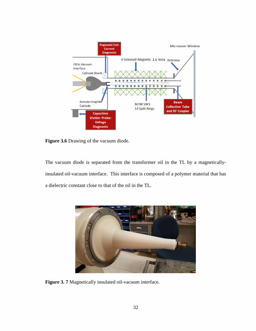
Figure 3.6 Drawing of the vacuum diode..........................................................................32
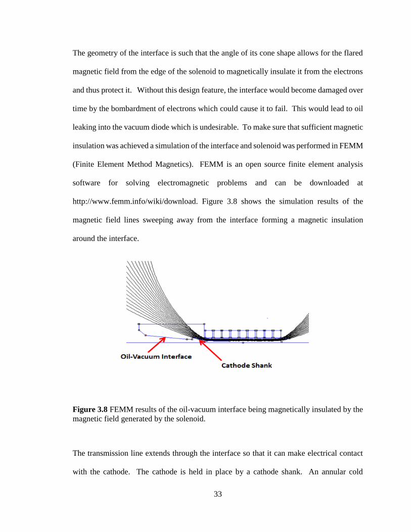
Figure 3.7 Magnetically insulated oil-vacuum interface..................................................32
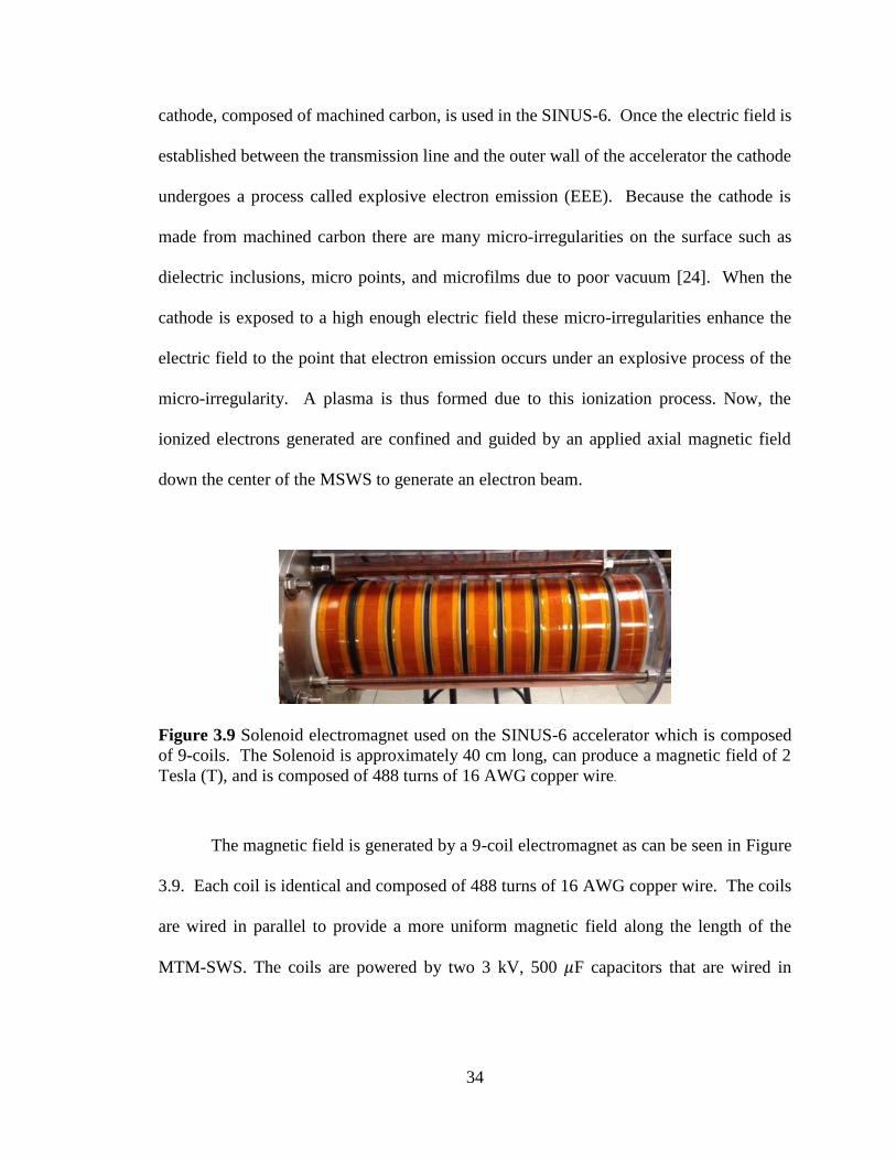
Figure 3.8 FEMM results of the oil-vacuum interface being magnetically insulated by the
magnetic field generated by the solenoid............................................................................33
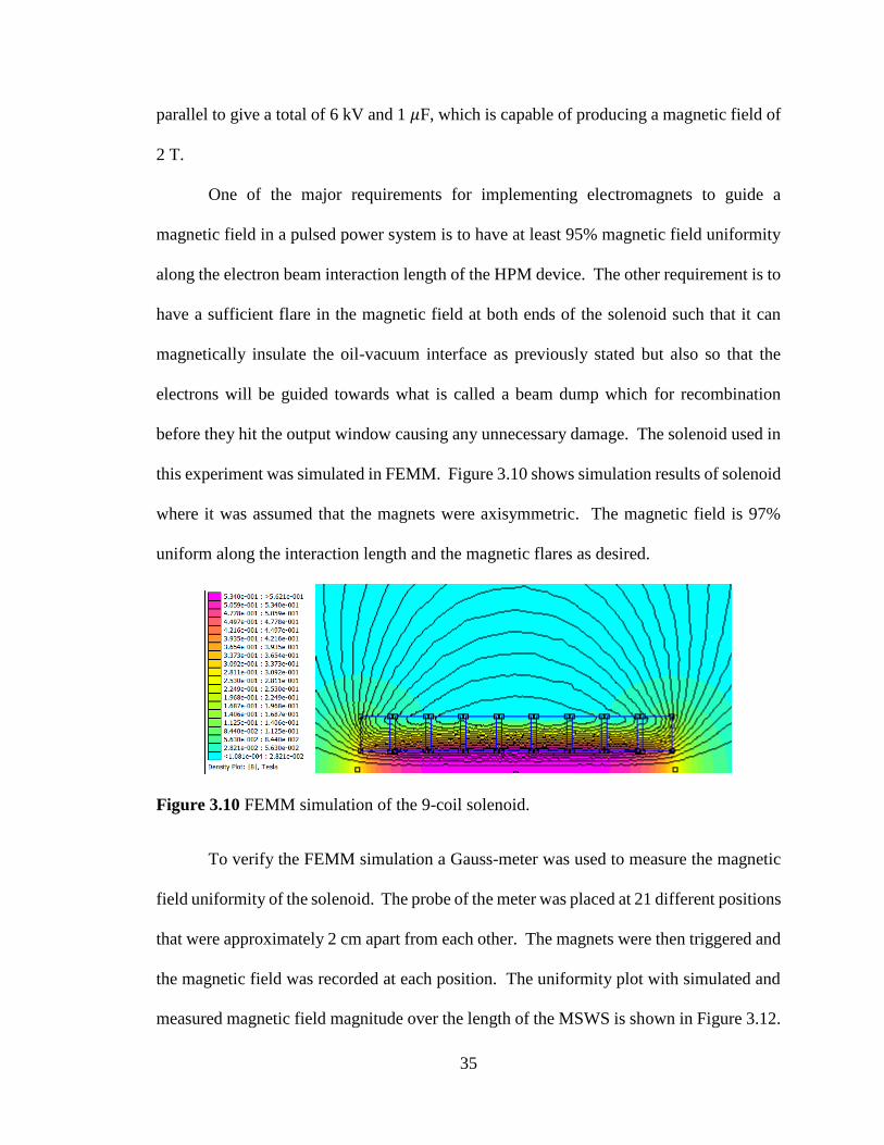
Figure 3.9 Solenoid electromagnet used on the SINUS-6 accelerator which is composed
of 9-coils. The Solenoid is approximately 40 cm long, can produce a magnetic field of 2
Tesla (T), and is composed of 488 turns of 16 AWG copper wire.......................................34
Figure 3.10 FEMM simulation of the 9-coil solenoid.......................................................35
Figure 3.11 Simulated and measured magnetic field distribution of the SINUS-6
solenoid..............................................................................................................................36
Figure 3.12 Rectangular cutoff waveguide positioned in front of conical horn antenna....38
Figure 3.13 Vertical field sweep with waveguide positioned at every 15 for a full 180
degrees...............................................................................................................................39
Figure 3.14 H10515B-20 Linear Array Multi-anode PMT developed by Hamamastu
Photonics............................................................................................................................40

x
Figure 3.15 Schematic of the PMT's face-plate and orientation of the 16 channels. The
dimensions are in mm [26] .................................................................................................41
Figure 3.16 Schematic of a simple PMT design [27] ........................................................42
Figure 3.17 CAD drawing of the Multi-Channel Fast Light Detector (MFLD).................43
Figure 3.18 Fiber optic head that is aligned with the PMT channels via the translation
stages..................................................................................................................................45
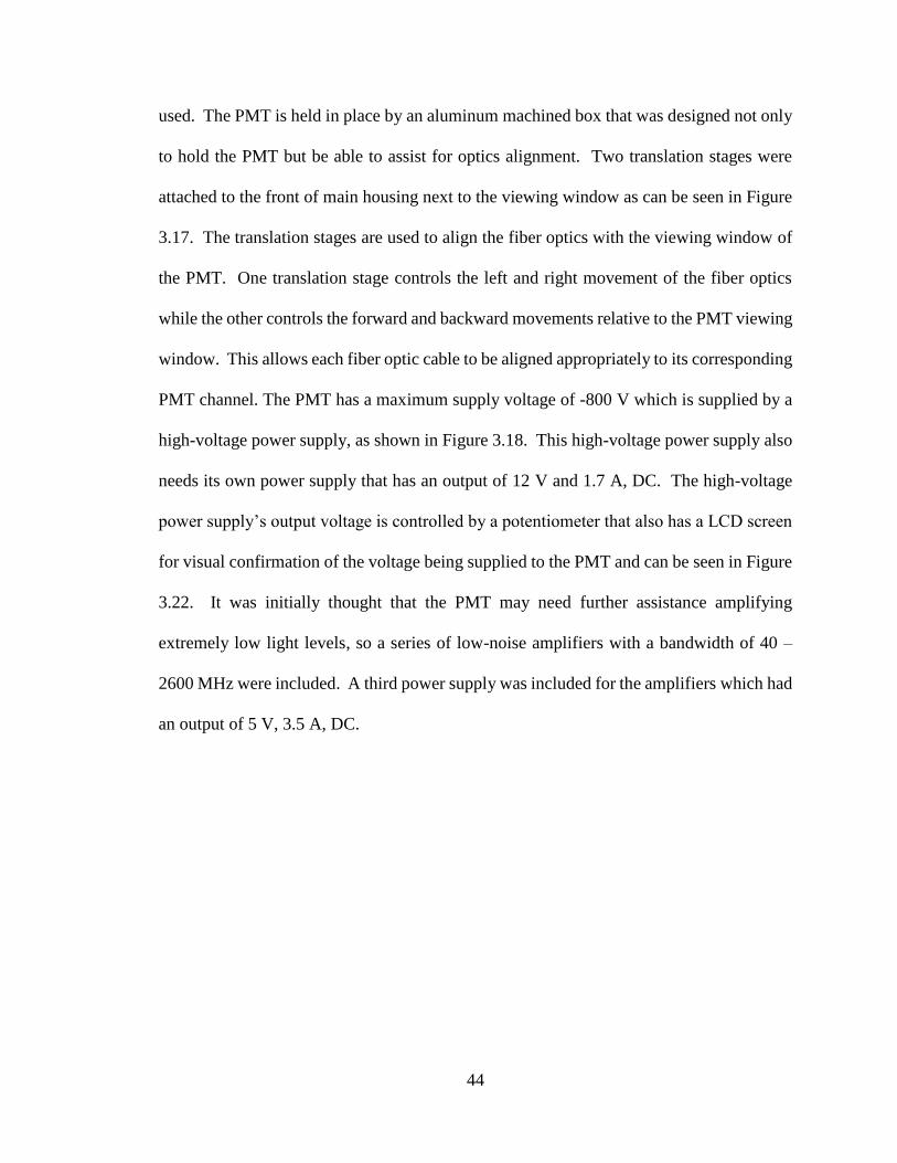
Figure 3.19 Inside view of the (MFLD)............................................................................46
Figure 3.20 Microstrip board that converts the pin output of the PMT to an SMA
connection..........................................................................................................................47
Figure 3.21 Inside view of the PMT, microstrip board, and SMA output of the Fast Light
Detector..............................................................................................................................48
Figure 3.22 Front, back, and side views of the Multi-Channel Fast Light Detector...........49
Figure 3.23 Spark gap used to test the MFLD...................................................................50
Figure 3.24 Oscilloscope trace of the MLFD measuring light from breakdown in the spark
gap. Voltage [mV] vs Time [500 𝜇s/div].......................................................................... 50
Figure 3.25 Optical mount for the collimating lenses that attaches to the front of the
antenna...............................................................................................................................51
Figure 3.26 Optical setup and view of the lenses down the MTM-SWS............................52
Figure 3.27 Final optical setup for the MFLD...................................................................53
Figure 3.28 Neon gas filled bulb array used for RF mode characterization placed in a 1x1
m foam board. The bulbs are spaced 2.5-cm apart.......................................................54
Figure 3.29 MATLAB generated field intensity patterns for TE-modes up to TE34..........55
Figure 3.30 MATLAB generated field intensity patterns for TM modes, up to TM34.......56
Figure 3.31 Left: image of unrectified neon bulb array. Right: rectified image of neon
bulb array...........................................................................................................................57
Figure 3.32 Centering method using moments of a gray-scaled image to find the centroid
based on the luma...............................................................................................................59
Figure 3.33 (Left) final cropped and centered image. (Right) Azimuthally, unwrapped
image which is interpolated to give lines of constant radial and poloidal dimensions. A
Pseudo-color in added to better show the calculated light intensity....................................60

xi
Figure 3.34 Average luma variation versus radial direction for the first 16 TE-modes....61
Figure 3.35 Average luma variation vs azimuthal dimension for the first 16 TE modes....61
Figure 3.36 Average luma variation versus radial direction for the first 16 TM-modes....62
Figure 3.37 Average luma variation versus azimuthal dimension for the first 16 TM
modes.................................................................................................................................62
Figure 4.1 MAGIC simulation results for the diode voltage (a), the input power (b), the
diode current (c), and the output power of MSWS (d). Provided by Dr. Sarita Prasad........63
Figure 4.2 MAGIC simulation results of MSWS's a.) RF signal measured at the output, b.)
a time frequency analysis of the signal, c.) a fast-Fourier transform of the RF signal, d.)
and the RF output mode. Provided by Dr. Sarita Prasad.....................................................64
Figure 4.3 HFSS simulation of MSWS's radiation pattern of the magnitude of the electric
field....................................................................................................................................66
Figure 4.4 CST simulation results of the azimuthal RF-field pattern as it exits the horn
antenna...............................................................................................................................67
Figure 4.5 MAGIC simulation results of voltage [kV], measured in between a.) rings and
b.) between the rings and the tube (inner wall of the cylindrical waveguide). Provided by
Dr. Sarita Prasad.................................................................................................................68
Figure 4.6 Normalized diode voltage and current signals..................................................69
Figure 4.7 a.) Measured RF-signal and b.) RF-signal with wave packet envelope
outlined..............................................................................................................................70
Figure 4.8 FFT of the MSWS showing the operational frequency of the device................71
Figure 4.9 Horizontal radiation pattern of MSWS. Measured with an L-band waveguide
detector...............................................................................................................................72
Figure 4.10 Vertical radiation pattern of MSWS measured with an L-band waveguide
detector...............................................................................................................................72
Figure 4.11 Breakdown measurements inside MSWS using the multi-channel fast light
detector (MFLD) from cathode..........................................................................................73
Figure 4.12 MFLD breakdown measurements with empty waveguide.............................74
Figure 4.13 Time-integrated, unfiltered visible light coming from cathode looking down
into the inside of the a.) MSWS and b.) the empty cylindrical waveguide. Both show that
the strongest light emission from the cathode is occurring in the location of channel 3,
which corresponds to the MFLD results. No other forms of breakdown were
verified...............................................................................................................................75

xii
Figure 4.14 Fast Oscilloscope traces of all the 4 channels used of the MLFD measurement
for breakdown within MSWS at 10.0-ns/div......................................................................76
Figure 4.15 Time integrated photo of the neon bulb array with the original camera
perspective on the left and the rectified image on the right.................................................77
Figure 4.16 Final cropped and centered image (a.) with its corresponding azimuthally
unwrapped image (b.). The unwrapped image has been interpolated so that lines of
constant 𝜌 and 𝜙 can be traversed during analysis. Pseudo-color is based on calculated
luma....................................................................................................................................78
Figure 4.17 Radial and poloidal averages of camera data compared with averages of the
calculated TE21 mode.........................................................................................................79
Figure 4.18 Radial and poloidal averages of camera data compared with averages of the
calculated TE12 mode.........................................................................................................80
Figure 4.19 Radial and poloidal averages of camera data compared with averages of the
calculated TE11 mode.........................................................................................................81
Figure 4.20 Rectified camera image (top left) compared to synthetically generated neon
bulb patterns TE21 (top right), TE11 (bottom left), and TE12 mode (bottom right)...........82

xiii
LIST OF TABLES
Table 2. 1 Expressions for the TM and TE field quantities for a circular waveguide in terms
of the axial components, derived from Eqns. (2.1) and (2.2) [1].......................................25
Table 4.1 MSWS RF pulse characteristics of rise time, fall-time, and pulse width........71
1
Chapter 1: INTRODUCTION
1.1 Background
The use of high power microwaves (HPM) has gained significant interest in the last 50
years. Since then, applications have been found in radar systems, nonlethal directed energy
weapons, space technologies, and nuclear fusion research. HPM sources are defined as
devices that exceed 100 MW in peak power and span the centimeter and millimeter wave
range of frequencies between 1 and 300 GHz [1]. The most conventional HPM sources are
derived from typical microwave sources such as the backward-wave oscillators (BWOs),
traveling wave tubes (TWTs), and magnetrons. In order for these devices to work, a pulsed
power system is used to inject a high current relativistic electron beam inside of the device
which is designed in such a way so that it takes the kinetic energy from the beam and
converts it into HPMs. The pulsed power systems used typically have pulse durations that
range anywhere from 10’s ns to 100’s ns [2]. One of the most successful examples of HPM
sources utilizing a relativistic electron beam is the relativistic BWO [3]. The BWO is
essentially a vacuum tube that contains a metallic periodic structure in which a relativistic
electron beam is injected axial through the center of the structure by the pulsed power
system. A strong axial magnetic field is used to confine and guide the beam through the
structure. As this beam moves through the structure it reduces the axial phase velocity of
the electromagnetic (EM) radiation generated, to less than the speed of light in which it can
couple with the electrons in the beam to produce microwaves. This type of structure is
called a slow-wave structure (SWS). Consequently, the SWS causes the electrons to
radiate in a manner analogous to electrons emitting Cerenkov radiation when they travel
2
through a medium at a speed greater than the local speed of light [4]. The area in which
the electron beam is affected by the SWS is called the interaction region. BWO’s are
classified as an O-type device or longitudinal device because they utilize an axial magnetic
field unlike an M-type device that guides the electrons across the electric and magnetic
fields such as a magnetron [4]. BWOs and their derivatives are some of the most versatile
of HPM sources, with gigawatt power levels demonstrated between within from 3 to 60-
GHz, and into L-band if desired [4].
Continued research in HPM sources is aimed at increasing radiation power, efficiency,
and the miniaturization of devices. One of the current areas of research is utilizing
metamaterials (MTMs) to achieve these aims, especially in the miniaturization of the
device. MTMs are artificially engineered composite materials that have properties that are
not found in natural materials. Some MTMs have unique electromagnetic properties called
double negative materials (DNGs). These materials (also known as left-handed materials)
were first purposed by Veselago in 1968 [5], in which he theorized the possibility of
obtaining solutions to Maxwell’s equations for wave propagation in a hypothetical medium
with a negative permittivity 𝜀(𝜔) < 0 and a negative permeability (𝜔) < 0 . Thirty years
later Pendry purposed a way to construct such a material [6], from microstructures that had
subwavelength dimensions compared with the wavelength of the electromagnetic radiation
they interacted with. These materials consisted of a nonmagnetic metallic wire which
provides the negative permittivity and a nonmagnetic split-ring resonator (SRR) which
provides the negative permeability. Using this theoretical work, Smith was able to
construct the first DNG material [7]. Researchers in many areas became interested in the
use of MTMs for differing applications. But, it wasn’t until 2008 when Marques published
3
a paper that led the way for the researchers in the HPM world to become excited about this
new frontier in material engineering. Marques, showed that a waveguide loaded with SRRs
operating below the cutoff frequency of the waveguide, provided a negative 𝜀 and 𝜇 within
a certain frequency band even though the transverse dimensions of the waveguide were
much smaller than the interacting wavelength [8]. This work meant that there was a
possibility for miniaturizing HPM sources using this MTM regime. Over the years much
theoretical and experimental work has been done on the use of MTMs in microwave
generation [9, 10, 11, 12, 13, 14, 15]. As of now, most of this research has been aimed at
using a MTM structures in an O-type device because it appears to be easier to construct
SRR structures axial down the interaction length of the device rather than constructing
them in an azimuthal interaction length as found in an M-type device.
This area of research sparked interest from the Air Force Office of Scientific
Research (AFOSR) which funded the Multidisciplinary Research Program of the
University of Research Initiative (MURI). This research initiative involves five universities
with the leadership of University of New Mexico (UNM). The other universities include
Massachusetts Institute of Technology (MIT), Louisiana State University (LSU), Ohio
State University (OSU), and the University of California Irvine (UCI). This funding
allowed for graduate students from their respective universities to develop and test
differing MTM HPM sources and applications.
The HPM source of interest in this thesis was developed at the UNM by, Dr. Prasad
and Dr. Yurt (see, [15] and [16]). This HPM source is classified as a BWO that is loaded
with 14 alternating split-rings that are broad-side coupled to each other. The split-rings
provide a negative permeability in the L-band frequency range and operating this structure
4
below the cutoff frequency of the BWO waveguide creates the negative electrical
permittivity. Thus, forming a metamaterial slow-wave structure (MSWS). Dr. Prasad and
Dr. Yurt, showed that they were able to reduce the transverse dimension of the HPM device
by utilizing this MTM owing to the concepts developed by [8] and [11].
Normally, a hollow, metallic, cylindrical BWO or waveguide requires a diameter that
is equivalent to one-half wavelength or more in order to support one or more transverse
electromagnetic modes. The operational frequency for UNM’s metamaterial MSWS
produces a negative permittivity and permeability is approximately 1.4-1.45 GHz.
Therefore, we can calculate the free-space wavelength by,
𝜆 =𝑐
𝑓 (1.1)
Where, 𝜆 is the wavelength, c is the speed of light (3x10⁸ m/s), and 𝑓 is the operating
frequency. Doing this calculation yields a 𝜆 ≈ 21 cm. Therefore, one half-wavelength is
≈ 10.5 cm. The inner diameter of UNM’s MSWS is 4.8 cm. This yields about a 54.3%
reduction in size of the transverse dimension. This is a substantial result because it allows
a desired HPM source to be much more compact and much more versatile, especially in
electronic warfare scenarios in which these devices could potentially be deployed in a
battlefield situation and used for electronic interference applications.
One of the issues of concern in using MTMs based devices in a HPM environment is
the potential for electrical breakdown inside the device. The main reason for this is
because, in such structures, the local field intensities within the unit cell of the structure
can be larger than the incident electric field intensity by several orders of magnitude.
5
Therefore, such structures are highly susceptible to breakdown even when illuminated by
moderate power levels [17]. Electrical breakdown inside these structures is undesirable
because it leads to an overall decrease in efficiency of the device and could potentially
damage it, as well. Therefore, it is important to develop a diagnostic that is able to detect
and measure any occurrence of breakdown in the device, but also the diagnostic should be
able to localize the breakdown so that the MTM HPM sources design could be optimized
appropriately.
One of the important aspects of any HPM source design, is to identify what
electromagnetic mode the HPM source will produce at a given frequency. An
electromagnetic mode describes how the electric and magnetic fields are oriented inside of
an HPM source relative to its imposed boundary conditions (i.e. the walls of the HPM
source) and its direction of propagation. In a hollow metallic waveguide or HPM source
there are ideally two independent classes of modes,
Transverse magnetic modes (TM, or E-modes) with no axial component of the
magnetic field (i.e. Bz = 0)
Transverse electric modes (TE, or H-modes) with no axial component of the
electric field (i.e., Ez = 0) [18].
The axial component is generally taken to be in the z-direction of a given coordinate system
and is referred to as the direction of wave propagation. A TM mode, has a magnetic field
that is transverse to the propagation direction of the electromagnetic wave and a TE mode
has an electric field that is transverse to the propagation direction of the wave. When the
HPM is extracted out of the source these modes will have an inherent polarization and
shape to the field intensities in space and time. Therefore, characterizing the exiting mode

6
is vital. Knowing what the output mode is, allows for us to know where the wave energy
is going to end up spatially over a given time as it radiates out into the environment. If the
source produces an undesirable mode, a mode converter could be utilized to convert the
natural mode of the device to a more desirable mode.
The purpose of this thesis is to extend the experimental work done on UNM’s MSWS.
This extension of experimentation will include further verification of diode voltage and
current measurements, RF frequency characterization, radiation pattern mapping, detection
of electrical breakdown inside the MSWS, and mode characterization. While [15] and [16]
have reported that UNM’s MSWS radiates TE21 mode based on MAGIC simulation results,
this still needs to be verified experimentally. To do this a couple of techniques will be
employed. The first technique used, is mapping the radiation pattern of the microwaves
exiting the antenna. This is done by taking a rectangular L-band waveguide detector and
putting it in the far-field of the radiation and taking measurements of the maximum electric
field amplitude of the radiation field (RF) at discrete intervals, horizontally around the
center of the radiating aperture of the antenna, as well as vertically, all the while keeping a
constant radial distance from the center of the aperture to the center of the waveguide
detector. This will produce a trace that shows the surface variation of the microwave
radiation produced by the MSWS. This can be correlated to the mode results that are given
in the simulation results of [15] and [16]. The second technique is to use an array of neon
gas filled bulbs that are not electrically connected to anything. These bulbs are placed in a
foam board in a 37x37 matrix that are evenly spaced apart from each other. The array is
placed in front of the radiating antenna such that the radiating electric field intensity will
breakdown the bulbs causing them to light up in a varying luminal intensity pattern that

7
correlates to the shape of the electrical field intensity pattern. Time integrated photographs
are taken with an SLR camera. Image analysis of these photographs is performed to find
the spatial luminal intensity variation of the bulbs which is then compared to theoretically
known and calculated electrical field intensity patterns of a cylindrical waveguide TE and
TM modes. A diagnostic has also been developed to detect, measure, and localize
breakdown inside of the MSWS. This was done by using a multi-channel photomultiplier
tube (PMT) with a sub-ns response time. It was used in-conjunction with external fiber
optics and lenses to capture any light emission produced from electrical breakdown within
the MSWS. The diagnostic is called the multi-channel fast light detector (MFLD) and will
be discussed later in chapter 3.
The research performed in this thesis was funded by the Air Force Office of Scientific
Research (AFOSR) within the Multidisciplinary Research Program of the University of
Research Initiative (MURI) under Grant FA9550-12-1-0489.
1.1.1: Organization of thesis
This thesis is organized as follows. In Chapter 2, the fundamentals of antenna radiation
patterns will be discussed, as well as the fundamentals of vacuum breakdown mechanisms,
and the fundamentals cylindrical modes.
Chapter 3 covers the experimental setup and methods. It will cover the MSWS setup
on the SINUS-6 electron beam accelerator, its basic operation and components. The
remaining sections in the chapter will show how diagnostics were setup and used to
characterize the frequency, map the field distribution, detect electrical breakdown inside
the MSWS, and characterize the mode.

8
Chapter 4 presents the simulation results and experimental results. The results
presented are the diode voltage and current measurements, the frequency analysis of the
RF-signal and RF-field mapping, the results of the breakdown detection, as well as the
characterization of the exiting RF mode from the MSWS.
Chapter 5 presents the conclusions and suggestions for future work.
9
CHAPTER 2: FUNDAMENTALS
2.1: Radiation Pattern Fundamentals
According to C. Balanis in, “Antenna Theory Analysis and Design, 4th ed.,”
An antenna radiation pattern or antenna pattern is defined as “a
mathematical function or a graphical representation of the radiation properties of
the antenna as a function of space coordinates. In most cases, the radiation pattern
is determined in the far-field region and is represented as a function of the
directional coordinates. Radiation properties include power flux density, radiation
intensity, field strength, directivity, phase or polarization [19].”
The pattern is developed by taking an observation point and moving horizontally or
vertically around while keeping a constant radius from the center of the radiating aperture
of the antenna and measuring either the field intensities or power density the radiation
coming out of the antenna. These field patterns can be represented as either a 2-
dimensional or 3-dimensional plot represents the surface of the radiation pattern, usually
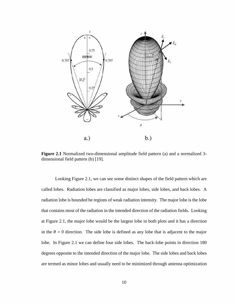
in the far-field. Figure 2.1 shows an example of what these plots may look like for a given
antenna. The measurements used to construct these plots are generally taken in the far-
field. It is much more difficult to acquire a 3-dimensional plot than a 2-dimensional plot
and are usually done through a modeling software program. The 2-dimesional pattern can
be acquired by making measurements of the electric field amplitudes at discrete steps along
an angular path around the center of the radiating part of the antenna while keeping a
constant radial distance from this point. A trace of the received electric or magnetic field
at a constant radius is called the amplitude field pattern [19]. These patterns are generally
normalized with respect to their maximum field value.
10
Figure 2.1 Normalized two-dimensional amplitude field pattern (a) and a normalized 3-
dimensional field pattern (b) [19].
Looking Figure 2.1, we can see some distinct shapes of the field pattern which are
called lobes. Radiation lobes are classified as major lobes, side lobes, and back lobes. A
radiation lobe is bounded be regions of weak radiation intensity. The major lobe is the lobe
that contains most of the radiation in the intended direction of the radiation fields. Looking
at Figure 2.1, the major lobe would be the largest lobe in both plots and it has a direction
in the 𝜃 = 0 direction. The side lobe is defined as any lobe that is adjacent to the major
lobe. In Figure 2.1 we can define four side lobes. The back-lobe points in direction 180
degrees opposite to the intended direction of the major lobe. The side lobes and back lobes
are termed as minor lobes and usually need to be minimized through antenna optimization
11
techniques. There are some cases in which these lobes could be useful but normally they
are undesirable.
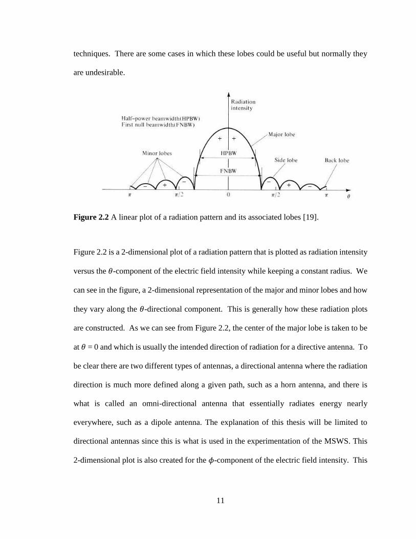
Figure 2.2 A linear plot of a radiation pattern and its associated lobes [19].
Figure 2.2 is a 2-dimensional plot of a radiation pattern that is plotted as radiation intensity
versus the 𝜃-component of the electric field intensity while keeping a constant radius. We
can see in the figure, a 2-dimensional representation of the major and minor lobes and how
they vary along the 𝜃-directional component. This is generally how these radiation plots
are constructed. As we can see from Figure 2.2, the center of the major lobe is taken to be
at 𝜃 = 0 and which is usually the intended direction of radiation for a directive antenna. To
be clear there are two different types of antennas, a directional antenna where the radiation
direction is much more defined along a given path, such as a horn antenna, and there is
what is called an omni-directional antenna that essentially radiates energy nearly
everywhere, such as a dipole antenna. The explanation of this thesis will be limited to
directional antennas since this is what is used in the experimentation of the MSWS. This
2-dimensional plot is also created for the 𝜙-component of the electric field intensity. This
12
can also be done for the magnetic field but it is much easier to measure the electric field
and therefore are usually either represented by the electric field or power density.
As stated before, the radiation pattern is usually measured in the far-field. There
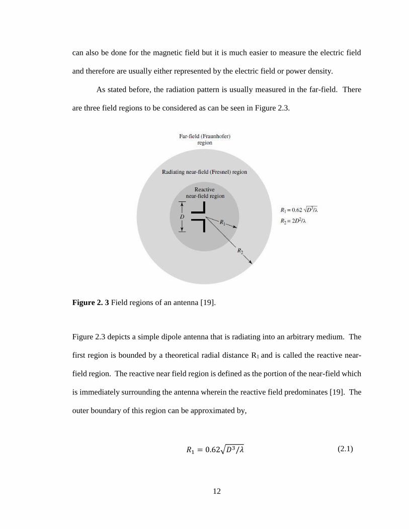
are three field regions to be considered as can be seen in Figure 2.3.
Figure 2. 3 Field regions of an antenna [19].
Figure 2.3 depicts a simple dipole antenna that is radiating into an arbitrary medium. The
first region is bounded by a theoretical radial distance R1 and is called the reactive near-
field region. The reactive near field region is defined as the portion of the near-field which
is immediately surrounding the antenna wherein the reactive field predominates [19]. The
outer boundary of this region can be approximated by,
𝑅1 = 0.62√𝐷3/𝜆 (2.1)
13
Where, D is the largest dimension of the radiating aperture of the antenna and 𝜆 is the
wavelength.
The next region of interest is the radiating near-field (Fresnel) region. In Figure
2.3 we can see that this region exists in between the reactive near-field region and the far-
field region. In this region, the angular field from the antenna starts to become dependent
upon the radial distance away from the antenna. The lower boundary is defined by Eqn.
(2.1) and its outer boundary is defined by
𝑅2 = 2𝐷2/𝜆 (2.2)
This criterion is based on a maximum phase error of 𝜋/8.
Last is the far-field (Fraunhofer) region. The far-field is defined as the region of
the field of an antenna where the angular field distribution is essentially independent of the
distance from the antenna [19]. The far field region exists from the radial distance R2 from
the antenna out to infinity. In this region, the field components are essentially transverse
and the angular distribution is independent of the radial distance where the measurements
are made [19].
In reality, the boundaries that were defined by Eqns. (2.1) and (2.2) really don’t
exist at discrete locations in space but exist as more of a continuum amongst each other
and these are only approximations, therefore we cannot necessarily define where these
boundaries exist with any clear precision and are based on a maximum phase error of 𝜋/8.
14
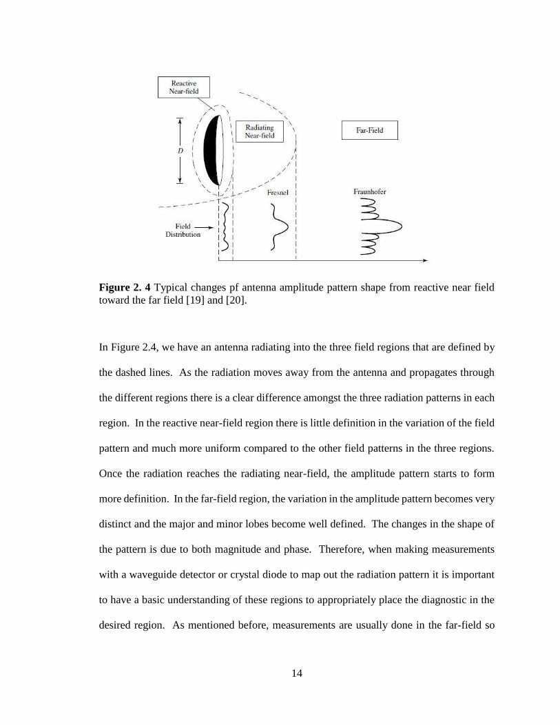
Figure 2. 4 Typical changes pf antenna amplitude pattern shape from reactive near field
toward the far field [19] and [20].
In Figure 2.4, we have an antenna radiating into the three field regions that are defined by
the dashed lines. As the radiation moves away from the antenna and propagates through
the different regions there is a clear difference amongst the three radiation patterns in each
region. In the reactive near-field region there is little definition in the variation of the field
pattern and much more uniform compared to the other field patterns in the three regions.
Once the radiation reaches the radiating near-field, the amplitude pattern starts to form
more definition. In the far-field region, the variation in the amplitude pattern becomes very
distinct and the major and minor lobes become well defined. The changes in the shape of
the pattern is due to both magnitude and phase. Therefore, when making measurements
with a waveguide detector or crystal diode to map out the radiation pattern it is important
to have a basic understanding of these regions to appropriately place the diagnostic in the
desired region. As mentioned before, measurements are usually done in the far-field so
15
that a well-defined plot of the field pattern can be obtained showing all the major and minor
lobes and thus a better graphical representation of the variations of the radiating surface.
2.2: Vacuum Breakdown Mechanisms
The production of HPM by using a particle beam in a SWS requires that the
structure be under a vacuum for proper insulation from any electrical breakdown. For an
ideal vacuum there is total absence of medium between the electrodes, there should be no
electrical breakdown at all [20]. However, at high applied voltages, breakdown still can
occur due to charge carriers being injected into the electrode gap. This creates the potential
for several breakdown mechanisms to occur in the system. These mechanisms originate
from having an imperfect vacuum making particle collisions possible, micro-protrusions
in the material or relatively small geometrical features in the design that can emit charge
carriers when exposed to high electric fields, or electrically weaker dielectric material that
aren’t robust enough to handle such harsh environments.
Vacuum is a very good insulator even at pd (pressure×density) < 10-3 Torr cm. At
these pressures and densities the electrons cross the electrode gap without any collisions
[20]. But electrical breakdown can still occurs. Therefore, it is important to understand the
mechanisms for breakdown in a vacuum.
One of these mechanisms is called the ABCD mechanism. This was introduced by
[21]. This mechanism produces breakdown when an electron emitted from the cathode
strikes the anode. This produces photons and positive ions, which they termed as C photons
and A positive ions. The A ions and the C photons then also strike the electrodes which
then produces B and D electrons respectively. This process continues causing an avalanche

16
mechanism producing more and more charged carriers until a breakdown channel is
formed. The condition for when electrical breakdown occurs is,
𝐴𝐵 + 𝐶𝐷 ≥ 1 (2.3)
The photons produced are either soft or hard X-rays caused by the impact of the
electrons. When the electrons and ions undergo recombination, they will emit photons that
are in the visible light or ultraviolet light spectrum. This process can occur when there are
impurities introduced into the vacuum from the electrodes, micro-protrusions in the
materials, or metal vapor in the system.
Field emission-initiated breakdown is another mechanism that is caused by micro-
protrusions on the electrodes of an HPM system. These protrusions, enhance the electric
field to such a point that they can emit electrons off the surface or even explode electrons
off into the system. The electric field enhancement can be approximated by,
𝐸𝑝 = 𝛽𝐸𝑎𝑣𝑔 =
𝛽𝑉
𝑑≈ (2 +
ℎ
𝑟) ∙
𝑉
𝑑 (2.4)
where, V is applied voltage, h is the height of the micro-projection, r is the radius of the
micro-projection, d is the gap between the anode and the cathode, and 𝛽 is the field
intensity factor that ~10 to 1000 [20]. This mechanism is highly dependent upon the
geometry of the micro-protrusion as well as the applied electric field. This type mechanism
has been shown to occur at electric fields and current densities on the order of 106-108
V/cm and 108-1010 A/cm2. Under these conditions enough charge carriers maybe released
17
to lead to the ABCD breakdown mechanism which would cause a further avalanching
effect leading to a breakdown channel forming within the vacuum system.
Plasma flare-initiated breakdown is another mechanism that is commonly found in
pulsed power vacuum systems. This type of breakdown takes place in a vacuum gap d on
the application of a high-voltage V short-duration ∆t pulse [20]. This mechanism is similar
to the field-emission breakdown mechanism in that it involves a micro-protrusion that
enhances the applied electric field except that it reaches such intensities that the protrusion
could actually explode generating a plasma flare. This will happen if the Joule energy
input of 𝐸𝑖 = 𝑖𝑐2 ∙ 𝑅 ∙ ∆𝑡 exceeds the energy given by a critical value 𝐸𝑐 given by
𝐸𝑐 = 𝑚[𝐶𝑝(𝑇𝑚 − 𝑇0) + 𝐿𝑣] (2.5)
Where 𝐶𝑝 is the specific heat of the material, 𝐿𝑣 latent heat of vaporization, 𝑇𝑚 is the
melting point of the electrode material, and 𝑇0 is the initial temperature [20]. When the
condition of 𝐸𝑖 > 𝐸𝑐, a plasma flare will form and then expand toward the anode which
then forms a breakdown channel between the cathode and the anode. This process can also
happen in the reverse direction where the plasma flare forms from the anode and bridges
the breakdown gap to the anode. This process for example could happen when an electron
beam generated by the cathode hits the anode with a high enough energy that it actually
explodes the material off of the anode producing a plasma flare.
The most common breakdown mechanism that occurs in a pulsed power/HPM
vacuum environment is a surface flash over on a relatively high dielectric material such as
a solid insulator. Typically, these types of materials are used for mechanical support in a

18
pulsed power system as well as interfaces that separate different media such as oil to
vacuum separation. These materials are electrically weaker than the metallic materials that
are used in these systems which makes them much more susceptible to breakdown. This
mechanism occurs when a high energy electron hits the dielectric material which causes a
secondary emission of electrons. These newly acquired electrons then can gain energy
from the applied electric field and in turn hit the dielectric they originated from causing
more electrons to be emitted from the dielectric. This leads to an avalanching effect that
can form a surface flash over breakdown inside the vacuum system. Dielectrics can
essentially act as a source of electrons. The constant bombardment of electrons will
eventually cause these dielectric materials to fail over time. To keep this from happening
the dielectrics are carefully designed so that their probability of having an electron impact
them is reduced as much as possible. Also, a lot of pulsed power systems will use magnetic
fields to guide high energy electrons away from the dielectric insulating them magnetically.
2.3: Cylindrical Waveguide Fundamentals
Waveguides act to confine and direct electromagnetic waves by imposing strict
boundary conditions on the wave. There are many different types of waveguides such as
hollow, metallic rectangular or cylindrical waveguides, coaxial waveguides, striplines,
microstrip lines, etc. The boundary conditions imposed by these waveguides cause the
waves to adopt specific modes that are dependent upon the size and shape of the device, as
well as the operating frequency. A mode is a particular field configuration relative to the
imposed boundary conditions and the propagation direction of the wave. There are three
different classes of the modes
19
Transverse electromagnetic mode (TEM, EH- or HE-mode) with both electric and
magnetic fields transverse to the propagation direction of the wave (Ez = Bz = 0).
Transverse magnetic modes (TM, or E-modes) with no magnetic field component
in the propagation direction of the wave (Bz = 0).
Transverse electric modes (TE, or H-modes) with no electric field component in
the propagation direction of the wave (Ez = 0).
For TEM, TM, and TE modes can propagate in a waveguide with two differing conductors
such as a parallel plate waveguide or a coaxial waveguide. But if there is only one
conductor such as in a hollow waveguide, then a TEM mode cannot be supported, but the
TE and TM modes can be. TE and TM modes will be the focus here since BWOs are
essentially single conductor hollow waveguides and can only support these principle
modes. There are instances where BWO’s and other HPM sources generate hybrid modes
or competing modes but discussion of these modes beyond the scope of this thesis and will
be omitted. In order to understand the modes that can exist in a cylindrical waveguide, a
derivation of the solutions for the electric and magnetic field will be presented for each
principle mode. These solutions are well known so this derivation will follow reference
[18].
Like always, in any electromagnetic problem we start off with the famous
Maxwell’s equations.
∇ × 𝑩 = 𝜇0𝒋 +1
𝑐2
𝜕𝑬
𝜕𝑡
(2.6)
20
∇ × 𝑬 = −
𝜕𝑩
𝜕𝑡
(2.7)
∇ ∙ 𝑩 = 0
(2.8)
∇ ∙ 𝑬 =
𝜌
𝜀0
(2.9)
Where, 𝑬 is the electric field and 𝑩 is the magnetic field. The source terms are 𝜌 and 𝒋 are
called the charge and current densities, respectively. For simplicity, let’s assume that the
walls of the waveguide are a perfect conductor. Therefore, the tangential electric field goes
to zero at any point x on the surface of the wall and the perpendicular magnetic field goes
to zero at any point x on the surface, as well. Therefore,
𝒏𝒕 ∙ 𝑬(𝑥) = 0 (2.10)
𝒏𝒑 ∙ 𝑩(𝑥) = 0 (2.11)
where, 𝒏𝒕 and 𝒏𝒑 are the tangential unit vector and normal unit vector to the surface,
respectively.
Now let’s assume that the waveguide with perfectly conducting walls, nor variation
of the cross section along the axis, and there is no electron beam or dielectric inside and
only a vacuum. First, we want to solve the wave equation for both the magnetic and electric
fields. Because we assumed no electrons or other sources the current density and charge
density go to zero in Maxwell’s Eqns. To solve for the magnetic field wave equation, we
take the curl of Eqn. (2.6) and plug Eqns. (2.7) and (2.8) to get
∇2𝑩 −
1
𝑐2
𝜕2𝑩
𝜕𝑡2= 0 (2.12)

21
And following a similar procedure for the electric wave equation, we take the curl of Eqn.
(2.7) and plug in Eqns. (2.6) and (2.9) and rearrange to get,
∇2𝑬 −
1
𝑐2
𝜕2𝑬
𝜕𝑡2 = 0 (2.13)
Because we have assumed axial symmetry and the medium in the waveguide is a vacuum
we can assume that the electric and magnetic field vary in space in time in the form
𝑬(𝒙, 𝑡) = 𝑬(𝒙⊥)exp [𝑖(𝑘𝑧𝑧 − 𝜔𝑡)] (2.14)
Where, 𝒙⊥ is a vector in the plane perpendicular to the z-axis and 𝑘𝑧 is the wavenumber
along the axial dimension of the waveguide and is equivalent to
𝑘𝑧 = 2𝜋/𝜆𝑤 (2.15)
Where, 𝜆𝑤 is the axial wavelength along the waveguide which is not equivalent to the
free space wave length shown in Eqn. (1.1).
We can write Eqn. (2.13) while using Eqn. (2.14), to we get a wave equation for
TM modes, which is expressed in terms of Ez component,
∇⊥
2 𝐸𝑧 − 𝑘𝑧2𝐸𝑧 +
𝜔2
𝑐2𝐸𝑧 = 0 (2.16)
And, repeating this procedure to Eqn. (2.12) to get a wave equation for TE modes we get

22
∇⊥
2 𝐵𝑧 − 𝑘𝑧2𝐵𝑧 +
𝜔2
𝑐2𝐵𝑧 = 0 (2.17)
Now, separating the cross-sectional variation from the axial variation and in time we get,
∇⊥2 𝐸𝑧 − 𝑘⊥,𝑇𝑀
2 𝐸𝑧 (2.18)
∇⊥2 𝐵𝑧 − 𝑘⊥,𝑇𝐸
2 𝐵𝑧 (2.19)
The wavenumbers 𝑘⊥,𝑇𝑀2 and 𝑘⊥,𝑇𝐸
2 are dependent upon the cross-sectional size and shape of
the waveguide. These are the wavenumber, also known as, the eigenvalues. Because they
have this dependency on the cross-sectional dimensions of the waveguide they can be
defined in terms of the cutoff frequency (𝜔𝑐𝑜) and the speed of light (c).
𝜔𝑐𝑜 = 𝑘⊥,𝑇𝑀𝑐 (2.20)
𝜔𝑐𝑜 = 𝑘⊥,𝑇𝐸𝑐 (2.21)
It is called the cutoff frequency because it is the minimum frequency at which a given mode
can propagate along the waveguide. Using Eqns. (2.18) and (2.19), we can rewrite Eqns.
(2.16) and (2.17) as,
23
(
𝜔2
𝑐2− 𝑘⊥,𝑇𝑀
2 − 𝑘𝑧2) 𝐸𝑧 = 0 (2.22)
(
𝜔2
𝑐2− 𝑘⊥,𝑇𝐸
2 − 𝑘𝑧2) 𝐵𝑧 = 0 (2.23)
Solving for the frequency 𝜔, and rearranging we can rewrite Eqns. (2.21) and (2.23) as
𝜔2 = 𝑘⊥,𝑇𝑀2 𝑐2 + 𝑘𝑧
2𝑐2 = 𝜔𝑐𝑜2 + 𝑘𝑧
2𝑐2 (2.24)
𝜔2 = 𝑘⊥,𝑇𝐸2 𝑐2 + 𝑘𝑧
2𝑐2 = 𝜔𝑐𝑜2 + 𝑘𝑧
2𝑐2 (2.25)
This is the dispersion relation. This relation tells everything one would need to know on
how a wave will propagate in a given medium or waveguide. The dispersion relation can
tell you the phase velocity (𝑣𝑝 = 𝜔/𝑘) and the group velocity 𝑣𝑔 = (𝜕𝜔/𝜕𝑘) of the wave,
what modes will propagate for specific frequencies ranges, what will the wave do at certain
frequencies such as reach a cutoff or resonant frequency, etc. Dispersion engineering is an
important part of HPM research and for the research of the UNM MSWS which was done
by Dr. Yurt (see [16]).
To continue on about waveguides. Using the same techniques in the previous
derivation we will now derive the TE and TM field solutions in a cylindrical waveguide
and apply the boundary conditions.
A cylindrical wave guide has a circular cross section, with a perfectly conducting
wall located at r = r0. Because we are working with a cylindrical geometry we use
cylindrical coordinates. Now we can write the electric and magnetic fields in the form

24
𝑬(𝑟, 𝜃, 𝑧, 𝑡) = 𝑬(𝑟, 𝜃)exp [𝑖(𝑘𝑧𝑧 − 𝜔𝑡)] (2.26)
Now following the same procedure as before we end up with wave equations in the
following forms
∇⊥
2 𝐸𝑧 =1
𝑟
𝜕
𝜕𝑟(𝑟
𝜕𝐸𝑧
𝜕𝑟) +
1
𝑟2
𝜕2𝐸𝑧
𝜕𝜃2= −𝑘⊥,𝑇𝑀𝐸𝑧 (2.27)
∇⊥
2 𝐵𝑧 =1
𝑟
𝜕
𝜕𝑟(𝑟
𝜕𝐵𝑧
𝜕𝑟) +
1
𝑟2
𝜕2𝐵𝑧
𝜕𝜃2= −𝑘⊥,𝑇𝐸𝐵𝑧 (2.28)
Now we apply the boundary conditions to the fields at r = r0 to Eqns. (2.27) and (2.28) and
solve for the solutions of the TM and TE fields.
𝑇𝐸 = 𝐵𝑟(𝑟 = 𝑟0) = 𝐸𝜃(𝑟 = 𝑟0) = 𝐸𝑧(𝑟 = 𝑟0) = 0 (2.29)
𝑇𝑀 = 𝐸𝑟(𝑟 = 𝑟0) = 𝐵𝜃(𝑟 = 𝑟0) = 𝐵𝑧(𝑟 = 𝑟0) = 0 (2.30)
Because we have cylindrical geometry, the solutions for the axial fields involve Bessel
functions of the first kind of order p, 𝐽𝑝. The eigenvalues for the TM modes involve the
roots of 𝐽𝑝.
𝐽𝑝(𝜇𝑝𝑛) = 0 (2.31)
The eigenvalues of the TE modes involve the derivatives of the roots of 𝐽𝑝.
𝑑𝐽𝑝(𝑥 = 𝜈𝑝𝑛)
𝑑𝑥= 0
(2.32)
25
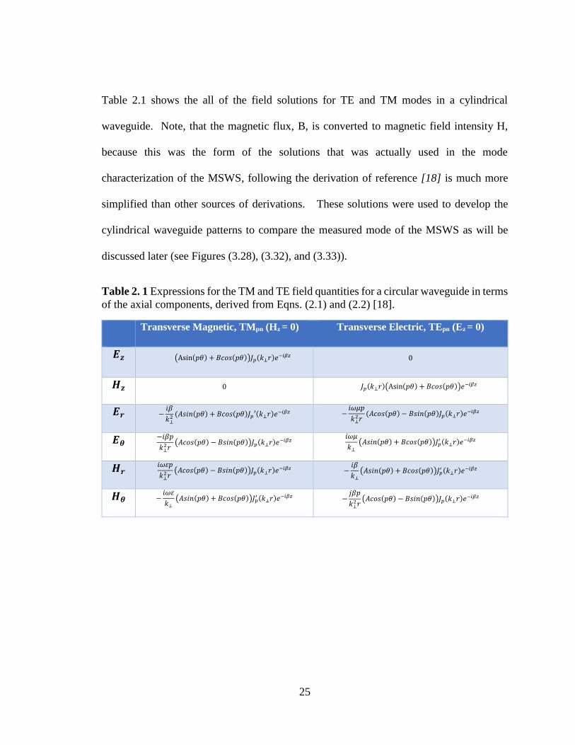
Table 2.1 shows the all of the field solutions for TE and TM modes in a cylindrical
waveguide. Note, that the magnetic flux, B, is converted to magnetic field intensity H,
because this was the form of the solutions that was actually used in the mode
characterization of the MSWS, following the derivation of reference [18] is much more
simplified than other sources of derivations. These solutions were used to develop the
cylindrical waveguide patterns to compare the measured mode of the MSWS as will be
discussed later (see Figures (3.28), (3.32), and (3.33)).
Table 2. 1 Expressions for the TM and TE field quantities for a circular waveguide in terms
of the axial components, derived from Eqns. (2.1) and (2.2) [18].
Transverse Magnetic, TMpn (Hz = 0) Transverse Electric, TEpn (Ez = 0)
𝑬𝒛 (Asin(𝑝𝜃) + 𝐵𝑐𝑜𝑠(𝑝𝜃))𝐽𝑝(𝑘⊥𝑟)𝑒−𝑖𝛽𝑧 0
𝑯𝒛 0 𝐽𝑝(𝑘⊥𝑟)(Asin(𝑝𝜃) + 𝐵𝑐𝑜𝑠(𝑝𝜃))𝑒−𝑖𝛽𝑧
𝑬𝒓 −𝑖𝛽
𝑘⊥2 (𝐴𝑠𝑖𝑛(𝑝𝜃) + 𝐵𝑐𝑜𝑠(𝑝𝜃)𝐽𝑝′(𝑘⊥𝑟)𝑒−𝑖𝛽𝑧 −
𝑖𝜔𝜇𝑝
𝑘⊥2𝑟
(𝐴𝑐𝑜𝑠(𝑝𝜃) − 𝐵𝑠𝑖𝑛(𝑝𝜃)𝐽𝑝(𝑘⊥𝑟)𝑒−𝑖𝛽𝑧
𝑬𝜽 −𝑖𝛽𝑝
𝑘⊥2𝑟
(𝐴𝑐𝑜𝑠(𝑝𝜃) − 𝐵𝑠𝑖𝑛(𝑝𝜃))𝐽𝑝(𝑘⊥𝑟)𝑒−𝑖𝛽𝑧 𝑖𝜔𝜇
𝑘⊥
(𝐴𝑠𝑖𝑛(𝑝𝜃) + 𝐵𝑐𝑜𝑠(𝑝𝜃))𝐽𝑝′ (𝑘⊥𝑟)𝑒−𝑖𝛽𝑧
𝑯𝒓 𝑖𝜔𝜀𝑝
𝑘⊥2𝑟
(𝐴𝑐𝑜𝑠(𝑝𝜃) − 𝐵𝑠𝑖𝑛(𝑝𝜃))𝐽𝑝(𝑘⊥𝑟)𝑒−𝑖𝛽𝑧 −𝑖𝛽
𝑘⊥
(𝐴𝑠𝑖𝑛(𝑝𝜃) + 𝐵𝑐𝑜𝑠(𝑝𝜃))𝐽𝑝′ (𝑘⊥𝑟)𝑒−𝑖𝛽𝑧
𝑯𝜽 −𝑖𝜔𝜀
𝑘⊥
(𝐴𝑠𝑖𝑛(𝑝𝜃) + 𝐵𝑐𝑜𝑠(𝑝𝜃))𝐽𝑝′ (𝑘⊥𝑟)𝑒−𝑖𝛽𝑧 −
𝑗𝛽𝑝
𝑘⊥2𝑟
(𝐴𝑐𝑜𝑠(𝑝𝜃) − 𝐵𝑠𝑖𝑛(𝑝𝜃))𝐽𝑝(𝑘⊥𝑟)𝑒−𝑖𝛽𝑧
26
CHAPTER 3: EXPERIMENTAL SETUP
3.1: MSWS Setup and SINUS-6 Electron Beam Accelerator
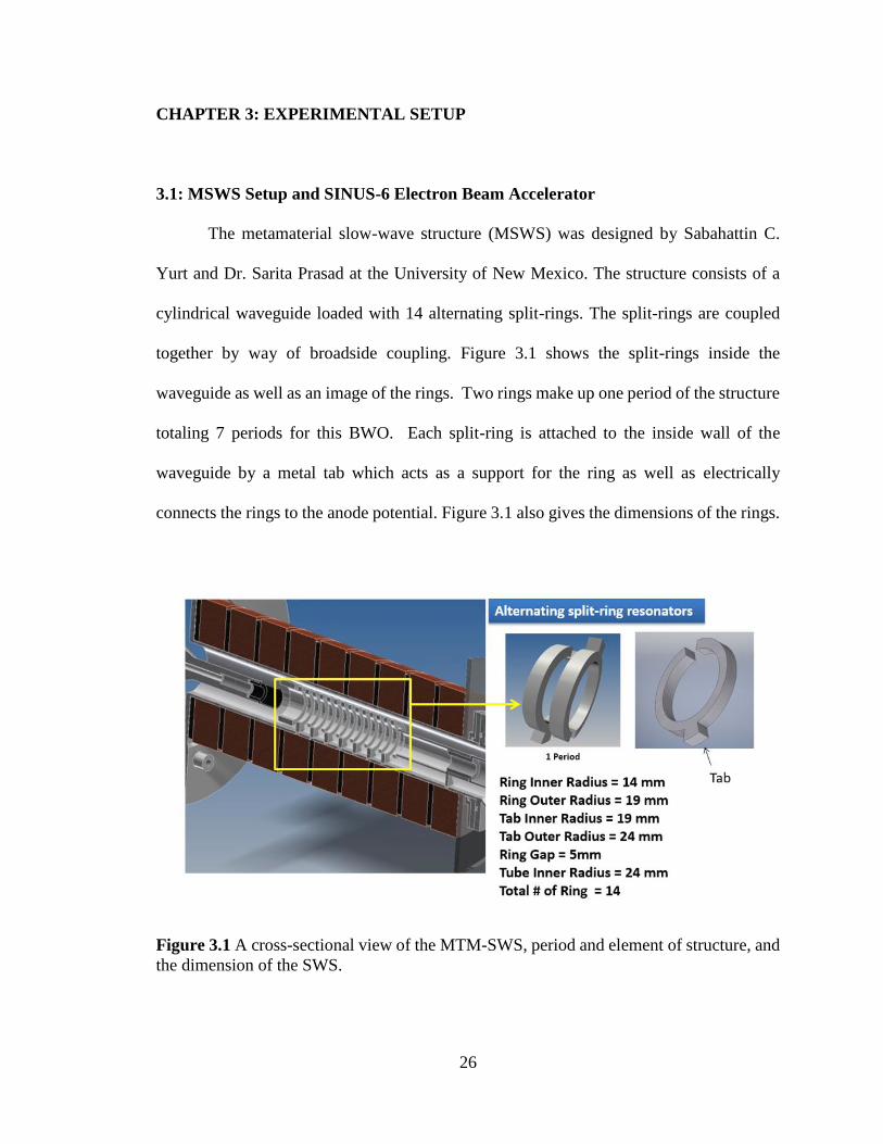
The metamaterial slow-wave structure (MSWS) was designed by Sabahattin C.
Yurt and Dr. Sarita Prasad at the University of New Mexico. The structure consists of a
cylindrical waveguide loaded with 14 alternating split-rings. The split-rings are coupled
together by way of broadside coupling. Figure 3.1 shows the split-rings inside the
waveguide as well as an image of the rings. Two rings make up one period of the structure
totaling 7 periods for this BWO. Each split-ring is attached to the inside wall of the
waveguide by a metal tab which acts as a support for the ring as well as electrically
connects the rings to the anode potential. Figure 3.1 also gives the dimensions of the rings.
Figure 3.1 A cross-sectional view of the MTM-SWS, period and element of structure, and
the dimension of the SWS.
27
There is a 0.5 cm spacing between the rings. The inner wall of the waveguide is 2.4 cm in
radius and approximately 40 cm in length. The MSWS is connected to an electron beam
accelerator called the SINUS-6. The center of the MSWS structure is carefully aligned to
the cathode such that the electron beam generated by the cathode will be guided down the
center of the rings by an axial magnetic field that is produced by a solenoid electromagnet.
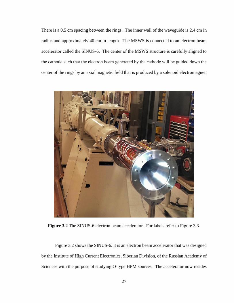
Figure 3.2 The SINUS-6 electron beam accelerator. For labels refer to Figure 3.3.
Figure 3.2 shows the SINUS-6. It is an electron beam accelerator that was designed
by the Institute of High Current Electronics, Siberian Division, of the Russian Academy of
Sciences with the purpose of studying O-type HPM sources. The accelerator now resides
28
at the University of New Mexico in Albuquerque, New Mexico where it used primarily for
HPM experiments in the Pulsed Power Lab headed by Dr. Edl Schamiloglu. The
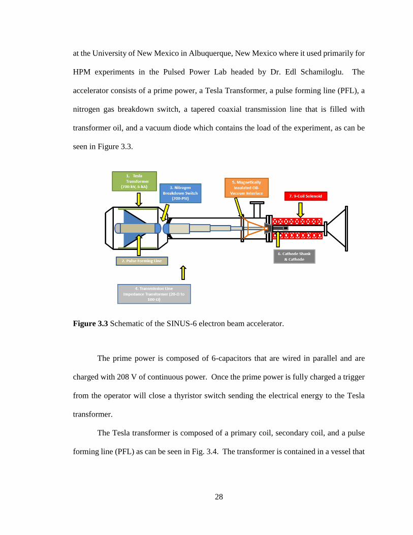
accelerator consists of a prime power, a Tesla Transformer, a pulse forming line (PFL), a
nitrogen gas breakdown switch, a tapered coaxial transmission line that is filled with
transformer oil, and a vacuum diode which contains the load of the experiment, as can be
seen in Figure 3.3.
Figure 3.3 Schematic of the SINUS-6 electron beam accelerator.
The prime power is composed of 6-capacitors that are wired in parallel and are
charged with 208 V of continuous power. Once the prime power is fully charged a trigger
from the operator will close a thyristor switch sending the electrical energy to the Tesla
transformer.
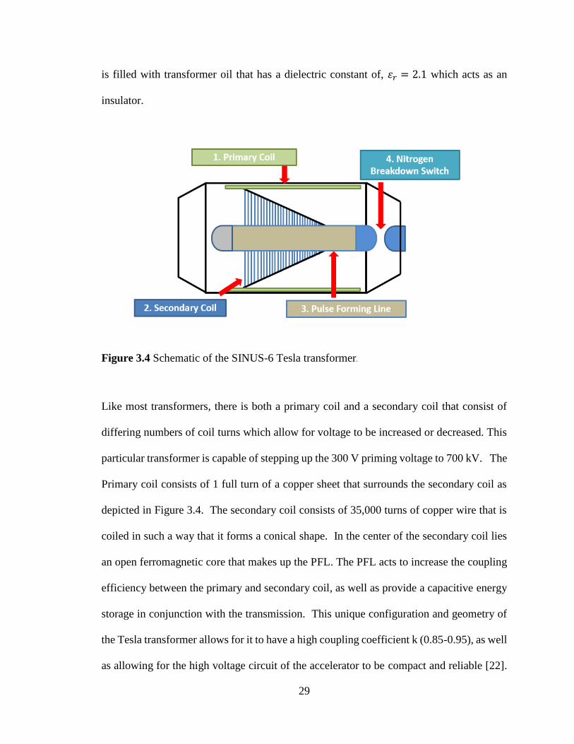
The Tesla transformer is composed of a primary coil, secondary coil, and a pulse
forming line (PFL) as can be seen in Fig. 3.4. The transformer is contained in a vessel that
29
is filled with transformer oil that has a dielectric constant of, 𝜀𝑟 = 2.1 which acts as an
insulator.
Figure 3.4 Schematic of the SINUS-6 Tesla transformer.
Like most transformers, there is both a primary coil and a secondary coil that consist of
differing numbers of coil turns which allow for voltage to be increased or decreased. This
particular transformer is capable of stepping up the 300 V priming voltage to 700 kV. The
Primary coil consists of 1 full turn of a copper sheet that surrounds the secondary coil as
depicted in Figure 3.4. The secondary coil consists of 35,000 turns of copper wire that is
coiled in such a way that it forms a conical shape. In the center of the secondary coil lies
an open ferromagnetic core that makes up the PFL. The PFL acts to increase the coupling
efficiency between the primary and secondary coil, as well as provide a capacitive energy
storage in conjunction with the transmission. This unique configuration and geometry of
the Tesla transformer allows for it to have a high coupling coefficient k (0.85-0.95), as well
as allowing for the high voltage circuit of the accelerator to be compact and reliable [22].

30
This allows charging of the PFL during the first half-period of the charging voltage if the
primary capacitive energy store does not exceed 1 kV [22].
The PFL has a few functions in this particular pulsed power system. It helps
increase coupling efficiency in the transformer during charging, it forms the voltage and
current pulse shapes of the accelerator, and it acts as a capacitive energy storage system
which forms the spark gap switch. The PFL makes up the core of the Tesla transformer, it
has a cylindrical shape of approximately 1.24 m with a 4.0 cm radius. This shape allows
for the SINUS-6’s voltage and current pulse shapes to resemble a half sinusoidal wave with
a transit time of approximately 12 ns. The output end of the PFL is in a nitrogen gas filled
chamber separated from the transformer oil by a solid dielectric interface. This forms a
capacitive energy storage that has a capacitance of 250 pF. The PFL is charged by the
Tesla transformer and has a charging time of approximately 60 𝜇𝑠. The PFL has an
impedance of 20 Ω which needs to be matched with the load in order for efficient energy
transfer to the load.
The switch of the SINUS-6 is a nitrogen gas filled spark-gap that is composed of
two electrodes, the first being the PFL and the other electrode being the input end of the
transmission line. The PFL acts as the cathode and the transmission line acts as the anode.
Both electrodes have a radius of approximately 4.0 cm with an electrode gap of
approximately 2.0 cm. The maximum gas pressure is 22 atmospheres [23]. This setup
creates a capacitor which is charged by the Tesla transformer. Once it is sufficiently
charged the switch closes sending the electrical energy down the transmission line to the
load.
31
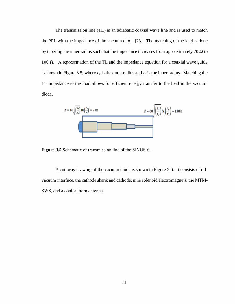
The transmission line (TL) is an adiabatic coaxial wave line and is used to match
the PFL with the impedance of the vacuum diode [23]. The matching of the load is done
by tapering the inner radius such that the impedance increases from approximately 20 Ω to
100 Ω. A representation of the TL and the impedance equation for a coaxial wave guide
is shown in Figure 3.5, where 𝑟𝑜 is the outer radius and 𝑟𝑖 is the inner radius. Matching the
TL impedance to the load allows for efficient energy transfer to the load in the vacuum
diode.
Figure 3.5 Schematic of transmission line of the SINUS-6.
A cutaway drawing of the vacuum diode is shown in Figure 3.6. It consists of oil-
vacuum interface, the cathode shank and cathode, nine solenoid electromagnets, the MTM-
SWS, and a conical horn antenna.
32
Figure 3.6 Drawing of the vacuum diode.
The vacuum diode is separated from the transformer oil in the TL by a magnetically-
insulated oil-vacuum interface. This interface is composed of a polymer material that has
a dielectric constant close to that of the oil in the TL.
Figure 3. 7 Magnetically insulated oil-vacuum interface.
33
The geometry of the interface is such that the angle of its cone shape allows for the flared
magnetic field from the edge of the solenoid to magnetically insulate it from the electrons
and thus protect it. Without this design feature, the interface would become damaged over
time by the bombardment of electrons which could cause it to fail. This would lead to oil
leaking into the vacuum diode which is undesirable. To make sure that sufficient magnetic
insulation was achieved a simulation of the interface and solenoid was performed in FEMM
(Finite Element Method Magnetics). FEMM is an open source finite element analysis
software for solving electromagnetic problems and can be downloaded at
http://www.femm.info/wiki/download. Figure 3.8 shows the simulation results of the
magnetic field lines sweeping away from the interface forming a magnetic insulation
around the interface.
Figure 3.8 FEMM results of the oil-vacuum interface being magnetically insulated by the
magnetic field generated by the solenoid.
The transmission line extends through the interface so that it can make electrical contact
with the cathode. The cathode is held in place by a cathode shank. An annular cold
34
cathode, composed of machined carbon, is used in the SINUS-6. Once the electric field is
established between the transmission line and the outer wall of the accelerator the cathode
undergoes a process called explosive electron emission (EEE). Because the cathode is
made from machined carbon there are many micro-irregularities on the surface such as
dielectric inclusions, micro points, and microfilms due to poor vacuum [24]. When the
cathode is exposed to a high enough electric field these micro-irregularities enhance the
electric field to the point that electron emission occurs under an explosive process of the
micro-irregularity. A plasma is thus formed due to this ionization process. Now, the
ionized electrons generated are confined and guided by an applied axial magnetic field
down the center of the MSWS to generate an electron beam.
Figure 3.9 Solenoid electromagnet used on the SINUS-6 accelerator which is composed
of 9-coils. The Solenoid is approximately 40 cm long, can produce a magnetic field of 2
Tesla (T), and is composed of 488 turns of 16 AWG copper wire.
The magnetic field is generated by a 9-coil electromagnet as can be seen in Figure
3.9. Each coil is identical and composed of 488 turns of 16 AWG copper wire. The coils
are wired in parallel to provide a more uniform magnetic field along the length of the
MTM-SWS. The coils are powered by two 3 kV, 500 𝜇F capacitors that are wired in
35
parallel to give a total of 6 kV and 1 𝜇F, which is capable of producing a magnetic field of
2 T.
One of the major requirements for implementing electromagnets to guide a
magnetic field in a pulsed power system is to have at least 95% magnetic field uniformity
along the electron beam interaction length of the HPM device. The other requirement is to
have a sufficient flare in the magnetic field at both ends of the solenoid such that it can
magnetically insulate the oil-vacuum interface as previously stated but also so that the
electrons will be guided towards what is called a beam dump which for recombination
before they hit the output window causing any unnecessary damage. The solenoid used in
this experiment was simulated in FEMM. Figure 3.10 shows simulation results of solenoid
where it was assumed that the magnets were axisymmetric. The magnetic field is 97%
uniform along the interaction length and the magnetic flares as desired.
Figure 3.10 FEMM simulation of the 9-coil solenoid.
To verify the FEMM simulation a Gauss-meter was used to measure the magnetic
field uniformity of the solenoid. The probe of the meter was placed at 21 different positions
that were approximately 2 cm apart from each other. The magnets were then triggered and
the magnetic field was recorded at each position. The uniformity plot with simulated and
measured magnetic field magnitude over the length of the MSWS is shown in Figure 3.12.
36
We can see that the measured magnetic field agrees well with the FEMM simulation and
has 96% uniformity along the interaction length.
Figure 3.11 Simulated and measured magnetic field distribution of the SINUS-6 solenoid.
In order to make the magnetic field look DC to the interacting electrons the electromagnets
are triggered before the accelerator which has a pulse length of 3 ms. The accelerator is
then triggered when the magnetic field is at a maximum which is about ¼ of the way
through the magnet pulse. Because the accelerator’s pulse duration is 6 orders of
magnitude smaller than the pulse of the solenoid the magnetic field appears to be DC
relative to the electron beam. At the end of the structure there is a coaxial section that
serves two functions (refer to Figure 3.6). It helps extracting the microwaves out of the
structure and it also acts as a beam dump, giving a safe place for the electron beam to
0.00
0.20
0.40
0.60
0.80
1.00
0.0 10.0 20.0 30.0 40.0
Mag
ne
tic
Fie
ld [
T]
Length [cm]
Magnetic Field Distribution of the SINUS-6 Solenoid.
Simulated Magnetic Field Experimental Magnetic Field

37
deposit itself. The microwaves are thus extracted out into free space by using a conical
horn antenna as can be seen in Figure 3.6.
The SINUS-6 also has a couple of diagnostics built into it; a self-intergating
Rogowski coil and a capacitive divider probe. The Rogowski coil is used for measuring
the diode current. It consists of a coil that goes around the outside of the cathode as can be
seen Fig. 3.7. The capacitive divider probe is used to measure the vacuum diode voltage.
It is located just behind the oil-vacuum interface measuring the voltage in the oil section
of the transmission line because the resistance is higher than in vacuum thus reducing the
potential for breakdown. The diode voltage and current measurements are then read out
on a fast oscilloscope.
3.2: Frequency Characterization and RF-Field Mapping
The frequency and radiation pattern of the RF of the MSWS were characterized by
using a rectangular L-band open-ended waveguide detector. To characterize the frequency
the waveguide is placed in front of the antenna such that the RF is incident upon the open
end of the waveguide as can be seen in Figure 3.12. The RF is coupled into a coaxial cable
which delivers the signal to a fast oscilloscope which measures the wave packet of the RF
signal. A fast Fourier transform (FFT) of the signal is computed using a MATLAB code
to give the frequency.

38
Figure 3.12 Rectangular waveguide positioned in front of conical horn antenna.
To plot the radiation pattern of the RF, the input of the waveguide detector is placed
across from the axis of the antenna in the far-field. The radiation pattern is usually
measured in the far-field region and is represented as a function of the directional
coordinates [19]. The far-field extends from its inner boundary which is approximately a
distance or radius (R), from the radiating aperture of the antenna to infinity. The inner
boundary of the far-field can be approximated by,
𝑅 = 2𝐷2/𝜆 (3.1)
Where, D is the largest dimension of the radiating aperture of the antenna and 𝜆 is the
wavelength of the radiating RF. In this region, the field components are essentially
transverse and the angular distribution is independent of the radial distance where the
measurements are made [25]. R was estimated to be 0.4-m. Due to the limited amount of
space the waveguide could only be placed 0.5-m away from the antenna. This radial

39
distance from the axis antenna was held constant while only the angular position from the
waveguide to the antenna was varied every 15 degrees, a full 180 degrees around the front
of the horn antenna, to give both a horizontal and vertical profiles of the RF-field maximum
amplitude field pattern. Figure 3.13 shows overlapped images of the different angular
positions of the waveguide for the vertical sweep to obtain the field distribution which was
also done for the horizontal profile.
Figure 3.13 Vertical field sweep with waveguide positioned at every 15 for a full 180
degrees (Dmitrii Andreev provided photograph).
An oscilloscope was used to measure the RF voltage signal at each position. Three shots
were taken at each position, and the maximum peak-to-peak amplitude for the three shots
at each position were averaged and translated into a plot of average maximum peak-to-
peak voltage versus the angular position from the center of the antenna.
40
3.3: Optical Diagnostic for Breakdown Detection
MTM structures may be highly susceptible to breakdown because the local field
intensities within the unit cell of the structure can be larger than the incident electric field
intensity by several orders of magnitude, making them more susceptible to breakdown even
when illuminated by moderate power levels [26]. Additionally, metamaterial or not, the
HPM environment is already a likely place for electrical breakdown to occur so there is a
strong belief that this phenomenon will occur in the MTMS during its operation. To detect
the occurrence of breakdown a diagnostic was developed to measure the intensity of light
being emitted from the breakdown. Other functions include, being able to localize it within
the structure and also give a measurement of time when it occurs and how long it lasts for
relative to the HPM pulse. Because the SINUS-6’s pulse is only 12-ns, the diagnostic
needed to have a sub-nanosecond response time. It also needed to have high gain incase
only low levels of light from breakdown existed, and it also needed to have multiple
channels in order to help localize the breakdown and see how it propagated within the
structure. To accomplish this, the H101515B-20 16-channel linear array multi-anode
PMT, was chosen.
Figure 3.14 H10515B-20 Linear Array Multi-anode PMT developed by Hamamastu
Photonics.
41
This PMT which can be seen in Figure 3.14, has a 0.6-ns response time, a maximum gain
of 120-dB, and has 16 linear channels whose orientation and dimensions at the viewing
window of the PMT can be seen in Figure 3.15 (dimensions in mm).
Figure 3.15 Schematic of the PMT's face-plate and orientation of the 16 channels. The
dimensions are in mm [26].
A PMT is a vacuum tube consisting of an input window, a photocathode, focusing
electrodes, an electron multiplier and an anode usually sealed into an evacuated tube [27].
The PMT takes advantage of the photoelectric effect in which light can cause the emission
of free charge carriers such as electrons from a material. Figure 3.16 shows a schematic of
a simple PMT design. On the inside of the viewing window is the photocathode which
usually consists of a conducting alkali material which is deposited on the inside of the
window. The photocathode and anode are typically biased with a voltage usually on the
order of 1000 V. In this case, the H10515B-20 can be biased up to -800 V.
42
Figure 3.16 Schematic of a simple PMT [27].
The voltage sets up an electric field between the cathode and anode as well as lowers the
potential energy an electron would need to be emitted. As photons from the incident light
hit the photocathode, electrons are ejected from the photocathode and are accelerated by
the applied electric field towards the first dynode. The first dynode is part of a series of
dynodes which act as an electron multiplier. Each dynode is biased approximately 100 V
difference from its neighboring dynode. As the incident electrons from the photocathode
strike the first dynode, secondary electron emission occurs which releases more electrons.
The dynodes are designed in such a way that when secondary emission occurs the electrons
are focused on to the next sequential dynode causing more secondary emission multiplying
the number of free electrons which are then focused on to the next dynode. This process
repeats itself exponentially generating more and more free electrons that eventually get
focused onto the anode. The electrons are deposited on the anode causing a current to flow
through the anode out to peripheral supporting electronics and instruments that can transmit
and measure the electrical signal. This cascading electron process allows PMT’s to have a
very high gain and are known to be able to amplify a photon of light by 160 dBs while also
producing very little noise. This makes them excellent for low light detection experiments.
43
In order to make this H10515B-20 functional for this experiment a couple of things
needed to be done. First, there had to be a housing created to contain, protect, and provide
RF shielding for the PMT. This enclosure also had to be large enough to house some
supporting electronics such as the two power supplies needed to power the PMT, 16 low
noise amplifiers that could be used for further amplification, plus their power supply, and
a microstrip board developed to convert the output pin connections of the PMT to SMA
connections. There also needed to be a way to implement peripheral fiber-optics that would
allow the PMT to see inside the MSWS and deliver any light from the experiment to the
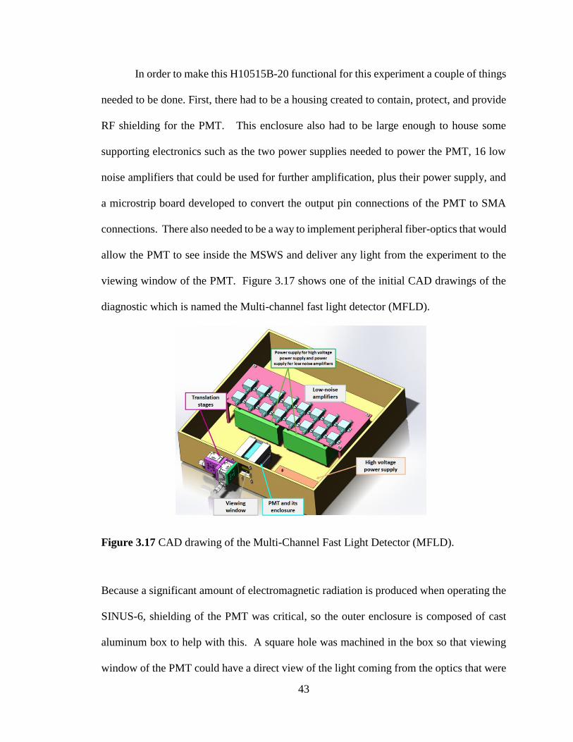
viewing window of the PMT. Figure 3.17 shows one of the initial CAD drawings of the
diagnostic which is named the Multi-channel fast light detector (MFLD).
Figure 3.17 CAD drawing of the Multi-Channel Fast Light Detector (MFLD).
Because a significant amount of electromagnetic radiation is produced when operating the
SINUS-6, shielding of the PMT was critical, so the outer enclosure is composed of cast
aluminum box to help with this. A square hole was machined in the box so that viewing
window of the PMT could have a direct view of the light coming from the optics that were
44
used. The PMT is held in place by an aluminum machined box that was designed not only
to hold the PMT but be able to assist for optics alignment. Two translation stages were
attached to the front of main housing next to the viewing window as can be seen in Figure
3.17. The translation stages are used to align the fiber optics with the viewing window of
the PMT. One translation stage controls the left and right movement of the fiber optics
while the other controls the forward and backward movements relative to the PMT viewing
window. This allows each fiber optic cable to be aligned appropriately to its corresponding
PMT channel. The PMT has a maximum supply voltage of -800 V which is supplied by a
high-voltage power supply, as shown in Figure 3.18. This high-voltage power supply also
needs its own power supply that has an output of 12 V and 1.7 A, DC. The high-voltage
power supply’s output voltage is controlled by a potentiometer that also has a LCD screen
for visual confirmation of the voltage being supplied to the PMT and can be seen in Figure
3.22. It was initially thought that the PMT may need further assistance amplifying
extremely low light levels, so a series of low-noise amplifiers with a bandwidth of 40 –
2600 MHz were included. A third power supply was included for the amplifiers which had
an output of 5 V, 3.5 A, DC.

45
Figure 3.18 Fiber optic head that is aligned with the PMT channels via the translation
stages.
Figure 3.18 shows the schematic of the fiber-optic-head that is attached to the
translation stages. The fiber optic head holds 16, 200-𝜇m, multimode, fiber optic cable
inputs that have an SMA input, which can be seen in Figure 3.19. These fibers terminate
at the holes shown above in the middle of the block, which were designed and spaced to
appropriately align with the channels on the viewing window of the PMT. The fibers and
translation stages are enclosed in their own enclosure that prevents them from being
damaged or misaligned. This enclosure was designed to provide easy access to the optics
and translations stages during experimentation for alignment adjustments. The enclosure
also helps keep out any external light that would saturate the PMT.
46
Figure 3.19 Inside view of the (MFLD).
As mentioned before the fiber-optics have an SMA input end that are connected to a male
to male SMA connector which are contained in a bulkhead as seen in Figure 3.19. This
allows for differing lengths and sizes of fiber optic patch cables to be connected to it for
varying experimental requirements. For this experiment four 50-ft, 200-𝜇m patch cables
were used in conjunction with four large beam collimating lenses which will be discussed
later.
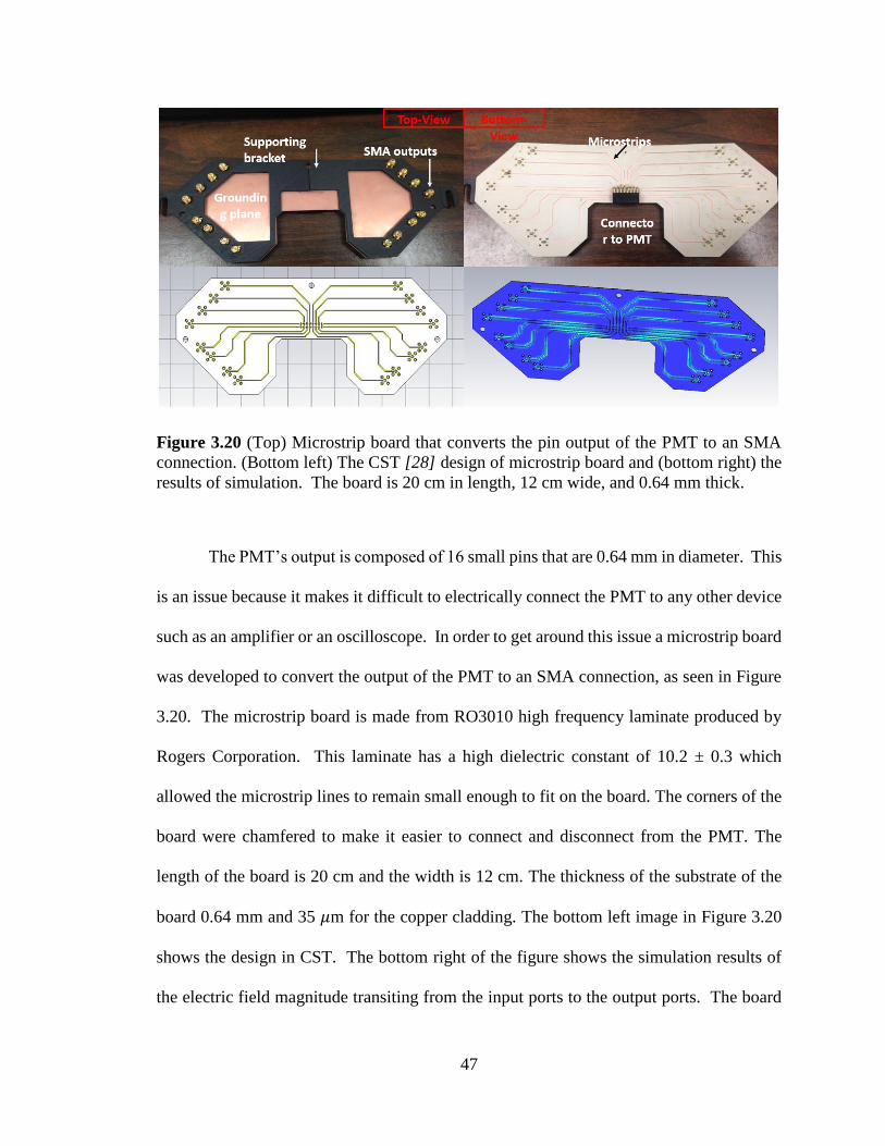
47
Figure 3.20 (Top) Microstrip board that converts the pin output of the PMT to an SMA
connection. (Bottom left) The CST [28] design of microstrip board and (bottom right) the
results of simulation. The board is 20 cm in length, 12 cm wide, and 0.64 mm thick.
The PMT’s output is composed of 16 small pins that are 0.64 mm in diameter. This
is an issue because it makes it difficult to electrically connect the PMT to any other device
such as an amplifier or an oscilloscope. In order to get around this issue a microstrip board
was developed to convert the output of the PMT to an SMA connection, as seen in Figure
3.20. The microstrip board is made from RO3010 high frequency laminate produced by
Rogers Corporation. This laminate has a high dielectric constant of 10.2 ± 0.3 which
allowed the microstrip lines to remain small enough to fit on the board. The corners of the
board were chamfered to make it easier to connect and disconnect from the PMT. The
length of the board is 20 cm and the width is 12 cm. The thickness of the substrate of the
board 0.64 mm and 35 𝜇m for the copper cladding. The bottom left image in Figure 3.20
shows the design in CST. The bottom right of the figure shows the simulation results of
the electric field magnitude transiting from the input ports to the output ports. The board
48
was simulated from 1 to 10 GHz and showed optimal performance from 1 GHz to 5 GHz.
In order to support the microstrip board a supporting bracket was designed and 3D-printed
as can be seen in the first image in Figure 3.20 in the top left as well as Figure 3.21. An
adhesive was used to adhere the supporting bracket to the ground plane side of the
microstrip board.
Figure 3.21 Inside view of the PMT, microstrip board, and SMA output of the Fast Light
Detector.
The microstrip board connects into the 16-pin output of the PMT and it essentially converts
the pin connection to an SMA connection as can be seen in Figure 3.22. Each microstrip
49
line and all of the SMA cables for each channel were kept at the same length so that there
wouldn’t be significant signal delays between channels.
Figure 3.22 Front, back, and side views of the Multi-Channel Fast Light Detector.
Figure 3.22 shows the front, back, and side views of the completed diagnostic. The
front end is equipped with the fiber optic inputs that transfer the light generated from the
experiment to the PMT to be converted to an electrical signal that can be measured on an
oscilloscope. On the back end of the MFLD are the SMA outputs that connect to the
oscilloscope via a coaxial SMA to SMA patch cable. There is also a power switch on the
back side of the PMT, as well as access to a potentiometer that controls the gain of the
PMT. On one of the sides there is an LCD screen that is used to read out the input voltage
to the PMT.
50
To test the MFLD, a spark gap was set up to create breakdown between two acorn
nuts as shown in Figure 3.23. The spark gap utilized a car ignition that was pulsed
repetitively by a frequency generator. Each channel was tested viewing the light emission
from the spark gap.
Figure 3.23 Spark gap used to test the MFLD.
Figure 3.24 Oscilloscope trace of the MLFD measuring light from breakdown in the spark
gap. Voltage [mV] vs Time [500 𝜇s/div].
51
Figure 3.24, shows an oscilloscope trace of the MLFD measuring the light being
emitted from the breakdown in the spark gap shown in Figure 3.23. The spark gap had a
pulse duration of about 500 𝜇𝑠. This was a positive test showing that the MLFD worked
for detecting light emission from electrical breakdown.
Due to the radial dimension of the MTMS being rather small only four channels
were used. Also, because there is no access at all into the vacuum diode the optics had to
be placed on the outside looking in through the front of the antenna window. The MFLD
was kept inside of a screen room to protect the electronics from harmful radiation. Four,
50 ft, 600 𝜇m, multimode fiber optic patch cables were used to connect the MFLD from
the screen room to four collimating lenses. The collimating lenses that were used are
F810SM-543 large beam collimating lenses, which were developed by Thor Labs. The
lenses were attached to the front of the antenna via a mount that was machined out of
acrylic as can be seen in Figure 3.25. Four circular grooves were machined into the mount
where the bolts attach it to the antenna allow for the lenses to be rotated and positioned
correctly.
Figure 3.25 Optical mount for the collimating lenses that attaches to the front of the
antenna.
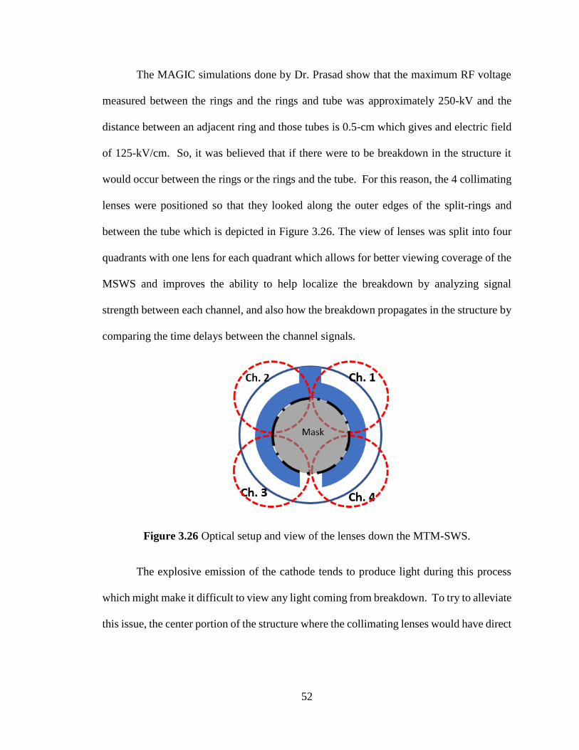
52
The MAGIC simulations done by Dr. Prasad show that the maximum RF voltage
measured between the rings and the rings and tube was approximately 250-kV and the
distance between an adjacent ring and those tubes is 0.5-cm which gives and electric field
of 125-kV/cm. So, it was believed that if there were to be breakdown in the structure it
would occur between the rings or the rings and the tube. For this reason, the 4 collimating
lenses were positioned so that they looked along the outer edges of the split-rings and
between the tube which is depicted in Figure 3.26. The view of lenses was split into four
quadrants with one lens for each quadrant which allows for better viewing coverage of the
MSWS and improves the ability to help localize the breakdown by analyzing signal
strength between each channel, and also how the breakdown propagates in the structure by
comparing the time delays between the channel signals.
Figure 3.26 Optical setup and view of the lenses down the MTM-SWS.
The explosive emission of the cathode tends to produce light during this process
which might make it difficult to view any light coming from breakdown. To try to alleviate
this issue, the center portion of the structure where the collimating lenses would have direct

53
view of the cathode was masked off using black electrical tape placed on the outside
antenna window. Figure 3.27 shows the final setup of the lenses on the SINUS-6.
Figure 3.27 Final optical setup for the MFLD.
3.4: Mode Characterization with a Neon Bulb Array
To verify the mode of the RF generated by the MSWS an array of neon gas filled
light bulbs was used. This array consisted of 37x37 matrix of neon bulbs set in a 1x1 m
foam board that was painted a matte black color to reduce reflection of light. The bulb
array was placed in front of the antenna as can be seen in Figure 3.28.
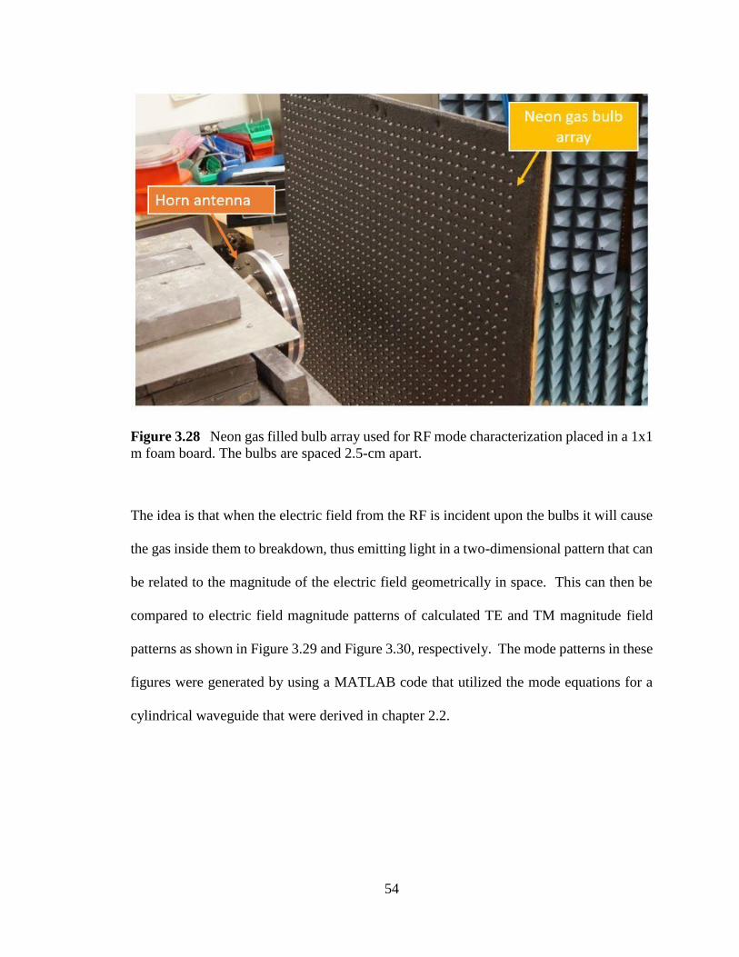
54
Figure 3.28 Neon gas filled bulb array used for RF mode characterization placed in a 1x1
m foam board. The bulbs are spaced 2.5-cm apart.
The idea is that when the electric field from the RF is incident upon the bulbs it will cause
the gas inside them to breakdown, thus emitting light in a two-dimensional pattern that can
be related to the magnitude of the electric field geometrically in space. This can then be
compared to electric field magnitude patterns of calculated TE and TM magnitude field
patterns as shown in Figure 3.29 and Figure 3.30, respectively. The mode patterns in these
figures were generated by using a MATLAB code that utilized the mode equations for a
cylindrical waveguide that were derived in chapter 2.2.
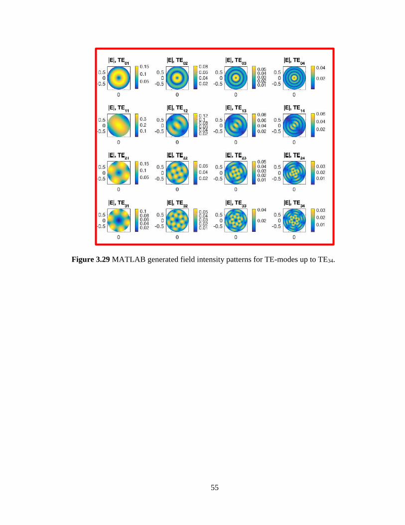
55
Figure 3.29 MATLAB generated field intensity patterns for TE-modes up to TE34.
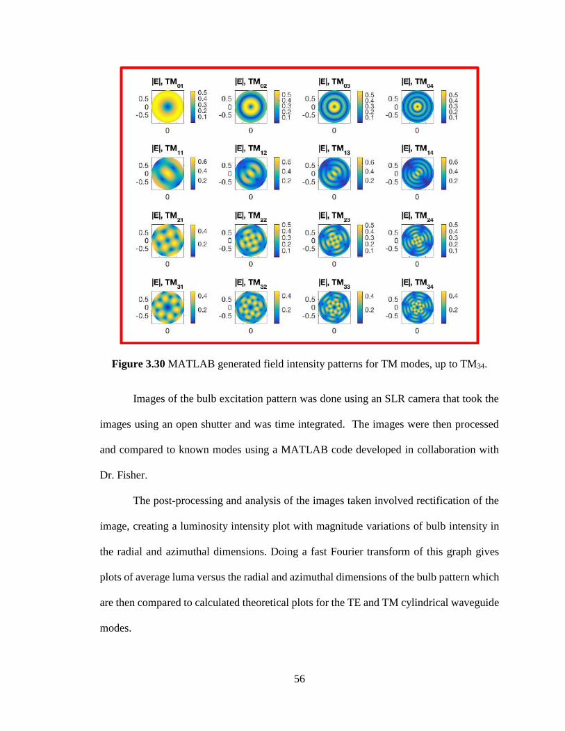
56
Figure 3.30 MATLAB generated field intensity patterns for TM modes, up to TM34.
Images of the bulb excitation pattern was done using an SLR camera that took the
images using an open shutter and was time integrated. The images were then processed
and compared to known modes using a MATLAB code developed in collaboration with
Dr. Fisher.
The post-processing and analysis of the images taken involved rectification of the
image, creating a luminosity intensity plot with magnitude variations of bulb intensity in
the radial and azimuthal dimensions. Doing a fast Fourier transform of this graph gives
plots of average luma versus the radial and azimuthal dimensions of the bulb pattern which
are then compared to calculated theoretical plots for the TE and TM cylindrical waveguide
modes.
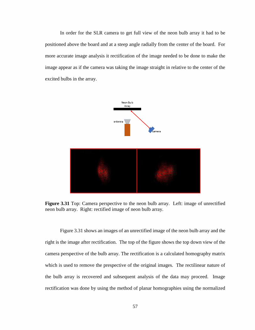
57
In order for the SLR camera to get full view of the neon bulb array it had to be
positioned above the board and at a steep angle radially from the center of the board. For
more accurate image analysis it rectification of the image needed to be done to make the
image appear as if the camera was taking the image straight in relative to the center of the
excited bulbs in the array.
Figure 3.31 Top: Camera perspective to the neon bulb array. Left: image of unrectified
neon bulb array. Right: rectified image of neon bulb array.
Figure 3.31 shows an images of an unrectified image of the neon bulb array and the
right is the image after rectification. The top of the figure shows the top down view of the
camera perspective of the bulb array. The rectification is a calculated homography matrix
which is used to remove the prespective of the original images. The rectilinear nature of
the bulb array is recovered and subsequent analysis of the data may proceed. Image
rectification was done by using the method of planar homographies using the normalized

58
direct linear transformation algorithm given by Hartkey and Zisserman [29]. Peter Kovesi
from University of Western Australia already produced an algorithm that uses this method
[30]. Points on a perspective image xPersp, correpsonding to points on a rectified image,
XRec, through a 3 x 3 homogeneous transformation matrix, H, called the homography
matrix
XRec = 𝐇xpersp
The above equation can be written as a set of two linear equations,
ℎ11𝑥 + ℎ12𝑦 + ℎ13 = ℎ31𝑥𝑋 + ℎ32𝑦𝑋 + ℎ33𝑋
ℎ21𝑥 + ℎ22𝑦 + ℎ23 = ℎ31𝑥𝑌 + ℎ32𝑦𝑌 + ℎ33𝑌
The homography matrix is then solved for the four-point pairs which then is used to rectify
the entire image into the appropriate perspective for analysis.
After rectification of the image is completed analysis is done to compare the
excitation pattern of the neon bulbs’ intensity with the calculated electric-field pattern
intensities in Figure 3.31. This is done by converting the RGB color of the image to a
luminance-based grayscale. The center of the neon bulb array is estimated based on the
perceived luminosity from the camera and by the moments of the image. The moments of
the image maybe expressed as
Mij = ∑ ∑ xiyjI(x, y)
yx
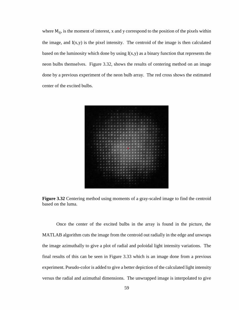
59
where Mij, is the moment of interest, x and y correspond to the position of the pixels within
the image, and I(x,y) is the pixel intensity. The centroid of the image is then calculated
based on the luminosity which done by using I(x,y) as a binary function that represents the
neon bulbs themselves. Figure 3.32, shows the results of centering method on an image
done by a previous experiment of the neon bulb array. The red cross shows the estimated
center of the excited bulbs.
Figure 3.32 Centering method using moments of a gray-scaled image to find the centroid
based on the luma.
Once the center of the excited bulbs in the array is found in the picture, the
MATLAB algorithm cuts the image from the centroid out radially in the edge and unwraps
the image azimuthally to give a plot of radial and poloidal light intensity variations. The
final results of this can be seen in Figure 3.33 which is an image done from a previous
experiment. Pseudo-color is added to give a better depiction of the calculated light intensity
versus the radial and azimuthal dimensions. The unwrapped image is interpolated to give
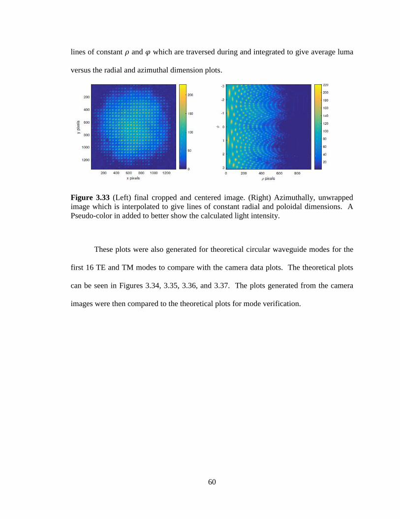
60
lines of constant 𝜌 and 𝜑 which are traversed during and integrated to give average luma
versus the radial and azimuthal dimension plots.
Figure 3.33 (Left) final cropped and centered image. (Right) Azimuthally, unwrapped
image which is interpolated to give lines of constant radial and poloidal dimensions. A
Pseudo-color in added to better show the calculated light intensity.
These plots were also generated for theoretical circular waveguide modes for the
first 16 TE and TM modes to compare with the camera data plots. The theoretical plots
can be seen in Figures 3.34, 3.35, 3.36, and 3.37. The plots generated from the camera
images were then compared to the theoretical plots for mode verification.
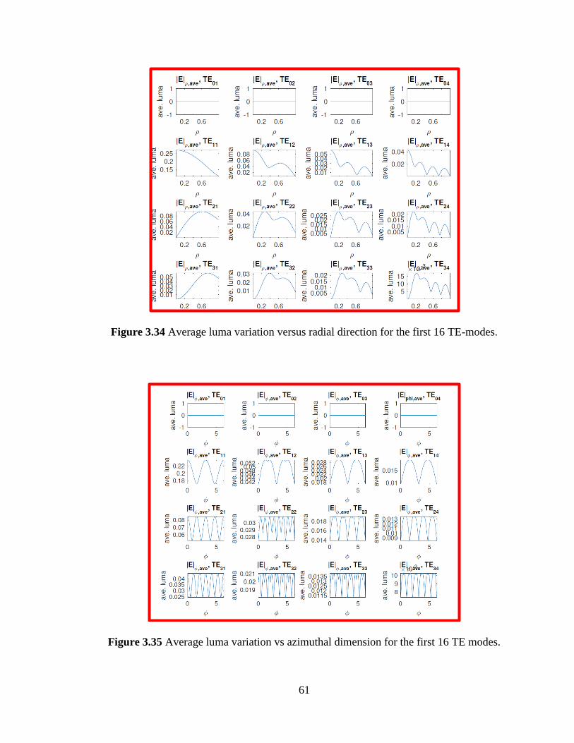
61
Figure 3.34 Average luma variation versus radial direction for the first 16 TE-modes.
Figure 3.35 Average luma variation vs azimuthal dimension for the first 16 TE modes.
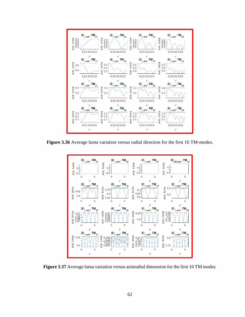
62
Figure 3.36 Average luma variation versus radial direction for the first 16 TM-modes.
Figure 3.37 Average luma variation versus azimuthal dimension for the first 16 TM modes.
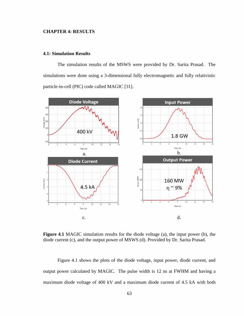
63
CHAPTER 4: RESULTS
4.1: Simulation Results
The simulation results of the MSWS were provided by Dr. Sarita Prasad. The
simulations were done using a 3-dimensional fully electromagnetic and fully relativistic
particle-in-cell (PIC) code called MAGIC [31].
Figure 4.1 MAGIC simulation results for the diode voltage (a), the input power (b), the
diode current (c), and the output power of MSWS (d). Provided by Dr. Sarita Prasad.
Figure 4.1 shows the plots of the diode voltage, input power, diode current, and
output power calculated by MAGIC. The pulse width is 12 ns at FWHM and having a
maximum diode voltage of 400 kV and a maximum diode current of 4.5 kA with both
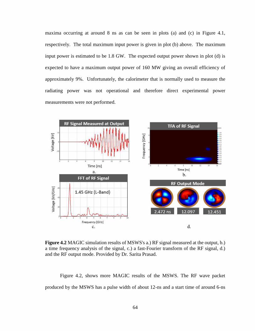
64
maxima occurring at around 8 ns as can be seen in plots (a) and (c) in Figure 4.1,
respectively. The total maximum input power is given in plot (b) above. The maximum
input power is estimated to be 1.8 GW. The expected output power shown in plot (d) is
expected to have a maximum output power of 160 MW giving an overall efficiency of
approximately 9%. Unfortunately, the calorimeter that is normally used to measure the
radiating power was not operational and therefore direct experimental power
measurements were not performed.
Figure 4.2 MAGIC simulation results of MSWS's a.) RF signal measured at the output, b.)
a time frequency analysis of the signal, c.) a fast-Fourier transform of the RF signal, d.)
and the RF output mode. Provided by Dr. Sarita Prasad.
Figure 4.2, shows more MAGIC results of the MSWS. The RF wave packet
produced by the MSWS has a pulse width of about 12-ns and a start time of around 6-ns

65
which is about half way through the accelerator pulse as can be seen in Figure 4.2. A fast
Fourier-transform was done of the RF time signal to measure the frequency of the RF pulse
as can be seen in plot (c). The MSWS’s frequency is approximately 1.45 GHz which lies
in the L-band. For further verification of the frequency a time frequency analysis was
performed showing that the dominate frequency of the MSWS is indeed 1.45 GHz. The
RF output mode is given in part (d) of Figure 4.2. It appears that the MSWS’s split rings
excite a “TE21-like” mode early on in the pulse at around 2.5 ns. This particular mode is
characterized by a “four-leaf clover” appearance of its electric fields with alternating
positive and negative field patterns which is given by the red and blue colors in Figure 4.2
(d), respectively. The TE21 mode is also known to have a null in electric field magnitude
at the center of its field patterns which is a characteristic that will be used to help identify
the mode during experimental measurements. As we can be seen in Figure 4.2 (d), At the
end of the pulse it appears the fields undergo a mode conversion and instead of having a
nice clean mode it appears to be a mixture of modes. This is could be caused by the change
in boundary conditions at the RF coupler which maybe causing a mode conversion due to
its geometry. Also, it isn’t really fully understood how the electric and magnetic fields will
orient themselves within a metamaterial structure due to the oscillating LC characteristics
of the split-rings. This could potentially give rise to competing modes being produced. At
this point it wasn’t apparent if mode characterization was going to possible.
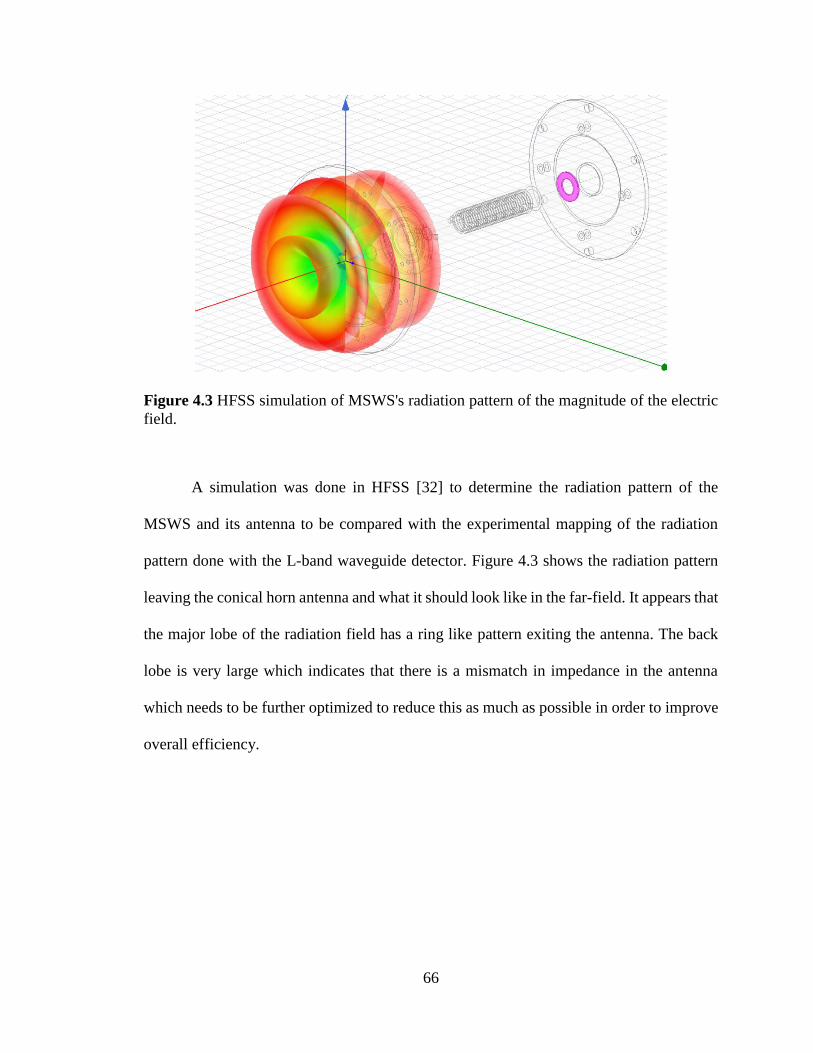
66
Figure 4.3 HFSS simulation of MSWS's radiation pattern of the magnitude of the electric
field.
A simulation was done in HFSS [32] to determine the radiation pattern of the
MSWS and its antenna to be compared with the experimental mapping of the radiation
pattern done with the L-band waveguide detector. Figure 4.3 shows the radiation pattern
leaving the conical horn antenna and what it should look like in the far-field. It appears that
the major lobe of the radiation field has a ring like pattern exiting the antenna. The back
lobe is very large which indicates that there is a mismatch in impedance in the antenna
which needs to be further optimized to reduce this as much as possible in order to improve
overall efficiency.
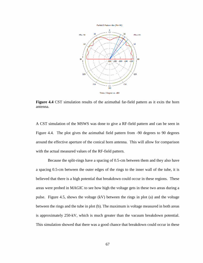
67
Figure 4.4 CST simulation results of the azimuthal far-field pattern as it exits the horn
antenna.
A CST simulation of the MSWS was done to give a RF-field pattern and can be seen in
Figure 4.4. The plot gives the azimuthal field pattern from -90 degrees to 90 degrees
around the effective aperture of the conical horn antenna. This will allow for comparison
with the actual measured values of the RF-field pattern.
Because the split-rings have a spacing of 0.5-cm between them and they also have
a spacing 0.5-cm between the outer edges of the rings to the inner wall of the tube, it is
believed that there is a high potential that breakdown could occur in these regions. These
areas were probed in MAGIC to see how high the voltage gets in these two areas during a
pulse. Figure 4.5, shows the voltage (kV) between the rings in plot (a) and the voltage
between the rings and the tube in plot (b). The maximum is voltage measured in both areas
is approximately 250-kV, which is much greater than the vacuum breakdown potential.
This simulation showed that there was a good chance that breakdown could occur in these
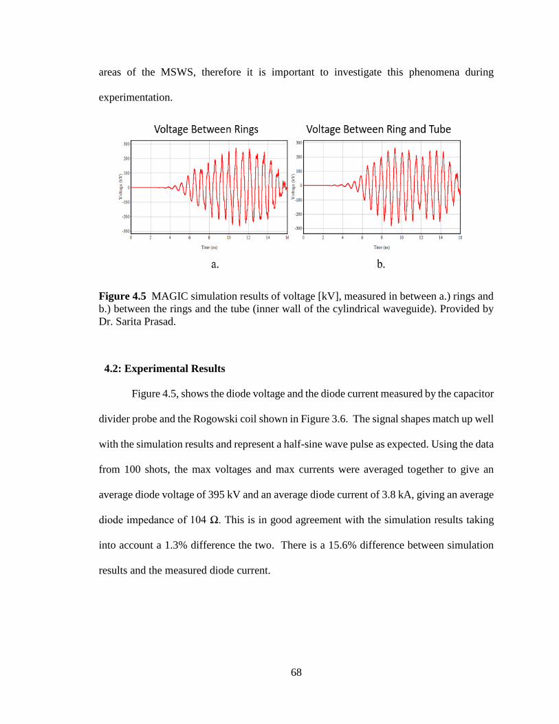
68
areas of the MSWS, therefore it is important to investigate this phenomena during
experimentation.
Figure 4.5 MAGIC simulation results of voltage [kV], measured in between a.) rings and
b.) between the rings and the tube (inner wall of the cylindrical waveguide). Provided by
Dr. Sarita Prasad.
4.2: Experimental Results
Figure 4.5, shows the diode voltage and the diode current measured by the capacitor
divider probe and the Rogowski coil shown in Figure 3.6. The signal shapes match up well
with the simulation results and represent a half-sine wave pulse as expected. Using the data
from 100 shots, the max voltages and max currents were averaged together to give an
average diode voltage of 395 kV and an average diode current of 3.8 kA, giving an average
diode impedance of 104 Ω. This is in good agreement with the simulation results taking
into account a 1.3% difference the two. There is a 15.6% difference between simulation
results and the measured diode current.
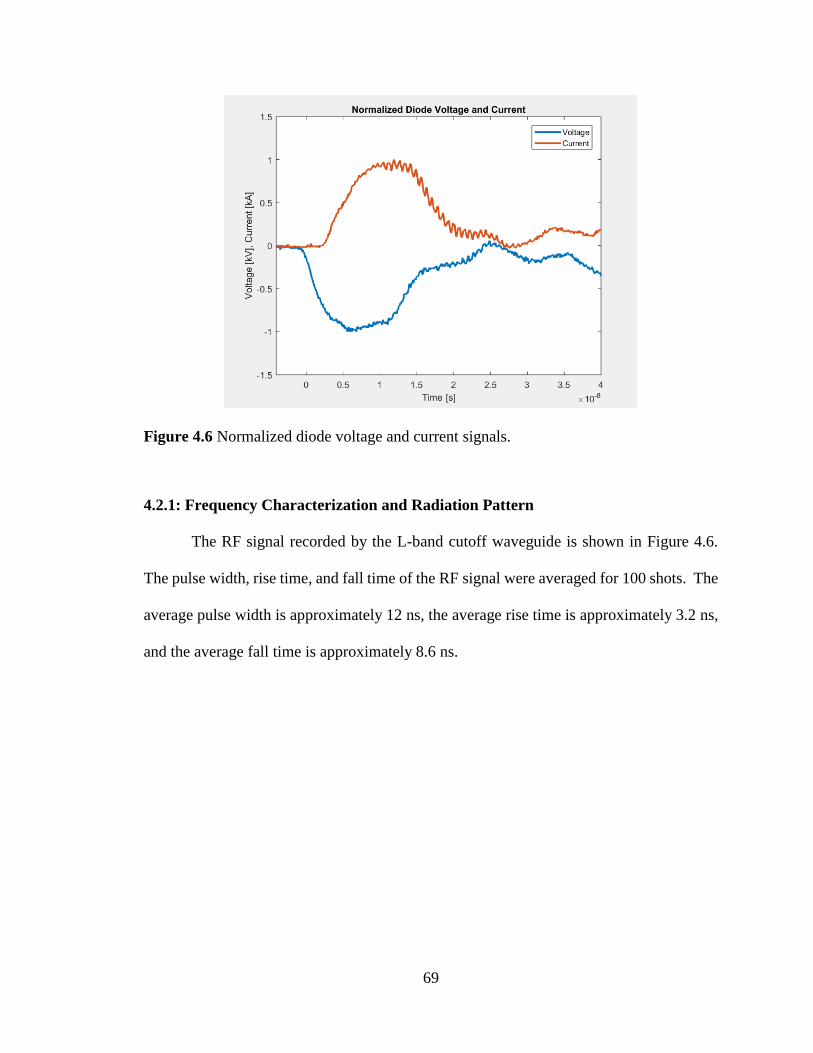
69
Figure 4.6 Normalized diode voltage and current signals.
4.2.1: Frequency Characterization and Radiation Pattern
The RF signal recorded by the L-band cutoff waveguide is shown in Figure 4.6.
The pulse width, rise time, and fall time of the RF signal were averaged for 100 shots. The
average pulse width is approximately 12 ns, the average rise time is approximately 3.2 ns,
and the average fall time is approximately 8.6 ns.
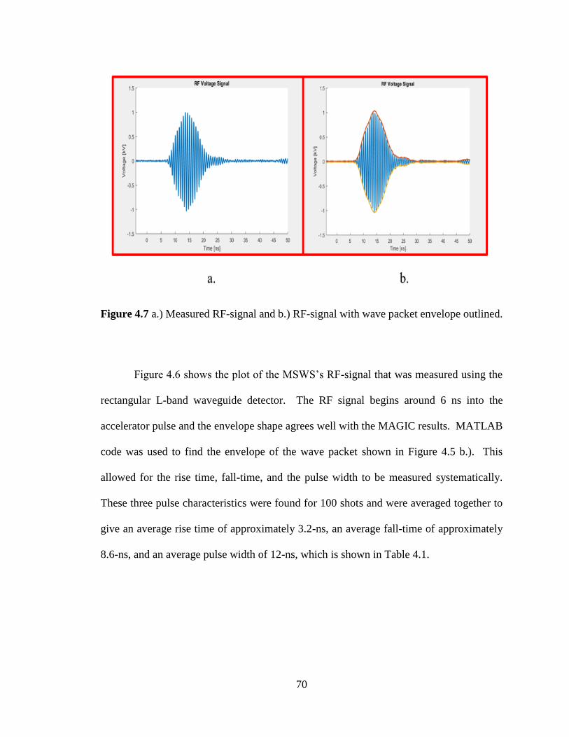
70
Figure 4.7 a.) Measured RF-signal and b.) RF-signal with wave packet envelope outlined.
Figure 4.6 shows the plot of the MSWS’s RF-signal that was measured using the
rectangular L-band waveguide detector. The RF signal begins around 6 ns into the
accelerator pulse and the envelope shape agrees well with the MAGIC results. MATLAB
code was used to find the envelope of the wave packet shown in Figure 4.5 b.). This
allowed for the rise time, fall-time, and the pulse width to be measured systematically.
These three pulse characteristics were found for 100 shots and were averaged together to
give an average rise time of approximately 3.2-ns, an average fall-time of approximately
8.6-ns, and an average pulse width of 12-ns, which is shown in Table 4.1.
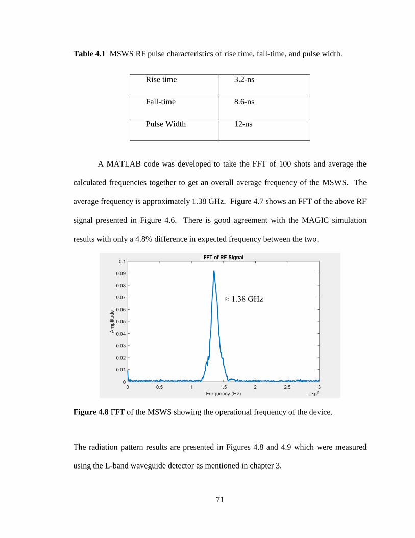
71
Table 4.1 MSWS RF pulse characteristics of rise time, fall-time, and pulse width.
Rise time 3.2-ns
Fall-time 8.6-ns
Pulse Width 12-ns
A MATLAB code was developed to take the FFT of 100 shots and average the
calculated frequencies together to get an overall average frequency of the MSWS. The
average frequency is approximately 1.38 GHz. Figure 4.7 shows an FFT of the above RF
signal presented in Figure 4.6. There is good agreement with the MAGIC simulation
results with only a 4.8% difference in expected frequency between the two.
Figure 4.8 FFT of the MSWS showing the operational frequency of the device.
The radiation pattern results are presented in Figures 4.8 and 4.9 which were measured
using the L-band waveguide detector as mentioned in chapter 3.
≈ 1.38 GHz
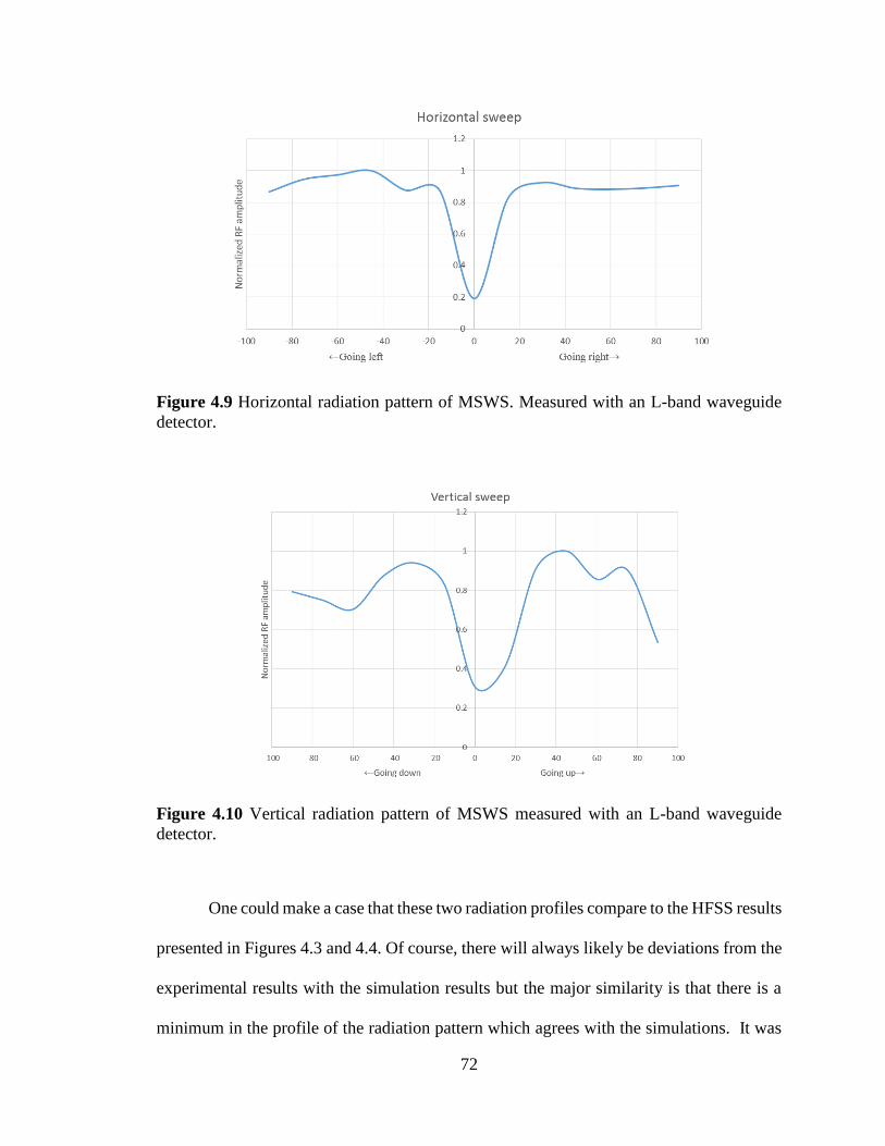
72
Figure 4.9 Horizontal radiation pattern of MSWS. Measured with an L-band waveguide
detector.
Figure 4.10 Vertical radiation pattern of MSWS measured with an L-band waveguide
detector.
One could make a case that these two radiation profiles compare to the HFSS results
presented in Figures 4.3 and 4.4. Of course, there will always likely be deviations from the
experimental results with the simulation results but the major similarity is that there is a
minimum in the profile of the radiation pattern which agrees with the simulations. It was
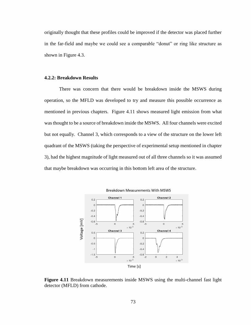
73
originally thought that these profiles could be improved if the detector was placed further
in the far-field and maybe we could see a comparable “donut” or ring like structure as
shown in Figure 4.3.
4.2.2: Breakdown Results
There was concern that there would be breakdown inside the MSWS during
operation, so the MFLD was developed to try and measure this possible occurrence as
mentioned in previous chapters. Figure 4.11 shows measured light emission from what
was thought to be a source of breakdown inside the MSWS. All four channels were excited
but not equally. Channel 3, which corresponds to a view of the structure on the lower left
quadrant of the MSWS (taking the perspective of experimental setup mentioned in chapter
3), had the highest magnitude of light measured out of all three channels so it was assumed
that maybe breakdown was occurring in this bottom left area of the structure.
Figure 4.11 Breakdown measurements inside MSWS using the multi-channel fast light
detector (MFLD) from cathode.
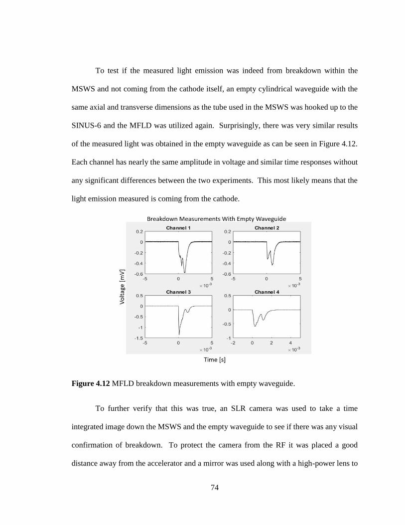
74
To test if the measured light emission was indeed from breakdown within the
MSWS and not coming from the cathode itself, an empty cylindrical waveguide with the
same axial and transverse dimensions as the tube used in the MSWS was hooked up to the
SINUS-6 and the MFLD was utilized again. Surprisingly, there was very similar results
of the measured light was obtained in the empty waveguide as can be seen in Figure 4.12.
Each channel has nearly the same amplitude in voltage and similar time responses without
any significant differences between the two experiments. This most likely means that the
light emission measured is coming from the cathode.
Figure 4.12 MFLD breakdown measurements with empty waveguide.
To further verify that this was true, an SLR camera was used to take a time
integrated image down the MSWS and the empty waveguide to see if there was any visual
confirmation of breakdown. To protect the camera from the RF it was placed a good
distance away from the accelerator and a mirror was used along with a high-power lens to
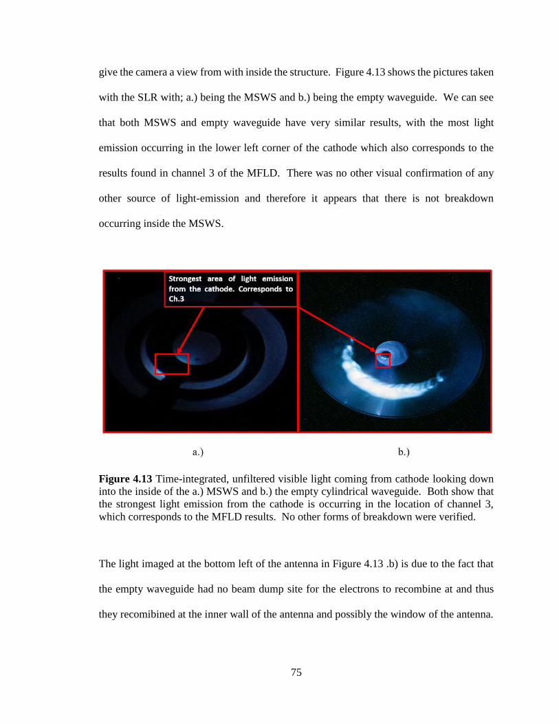
75
give the camera a view from with inside the structure. Figure 4.13 shows the pictures taken
with the SLR with; a.) being the MSWS and b.) being the empty waveguide. We can see
that both MSWS and empty waveguide have very similar results, with the most light
emission occurring in the lower left corner of the cathode which also corresponds to the
results found in channel 3 of the MFLD. There was no other visual confirmation of any
other source of light-emission and therefore it appears that there is not breakdown
occurring inside the MSWS.
Figure 4.13 Time-integrated, unfiltered visible light coming from cathode looking down
into the inside of the a.) MSWS and b.) the empty cylindrical waveguide. Both show that
the strongest light emission from the cathode is occurring in the location of channel 3,
which corresponds to the MFLD results. No other forms of breakdown were verified.
The light imaged at the bottom left of the antenna in Figure 4.13 .b) is due to the fact that
the empty waveguide had no beam dump site for the electrons to recombine at and thus
they recomibined at the inner wall of the antenna and possibly the window of the antenna.
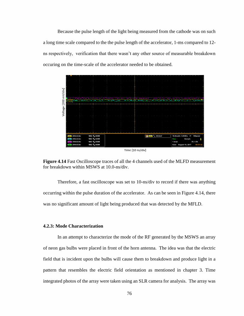
76
Because the pulse length of the light being measured from the cathode was on such
a long time scale compared to the the pulse length of the accelerator, 1-ms compared to 12-
ns respectively, verification that there wasn’t any other source of measurable breakdown
occuring on the time-scale of the accelerator needed to be obtained.
Figure 4.14 Fast Oscilloscope traces of all the 4 channels used of the MLFD measurement
for breakdown within MSWS at 10.0-ns/div.
Therefore, a fast oscilloscope was set to 10-ns/div to record if there was anything
occurring within the pulse duration of the accelerator. As can be seen in Figure 4.14, there
was no significant amount of light being produced that was detected by the MFLD.
4.2.3: Mode Characterization
In an attempt to characterize the mode of the RF generated by the MSWS an array
of neon gas bulbs were placed in front of the horn antenna. The idea was that the electric
field that is incident upon the bulbs will cause them to breakdown and produce light in a
pattern that resembles the electric field orientation as mentioned in chapter 3. Time
integrated photos of the array were taken using an SLR camera for analysis. The array was
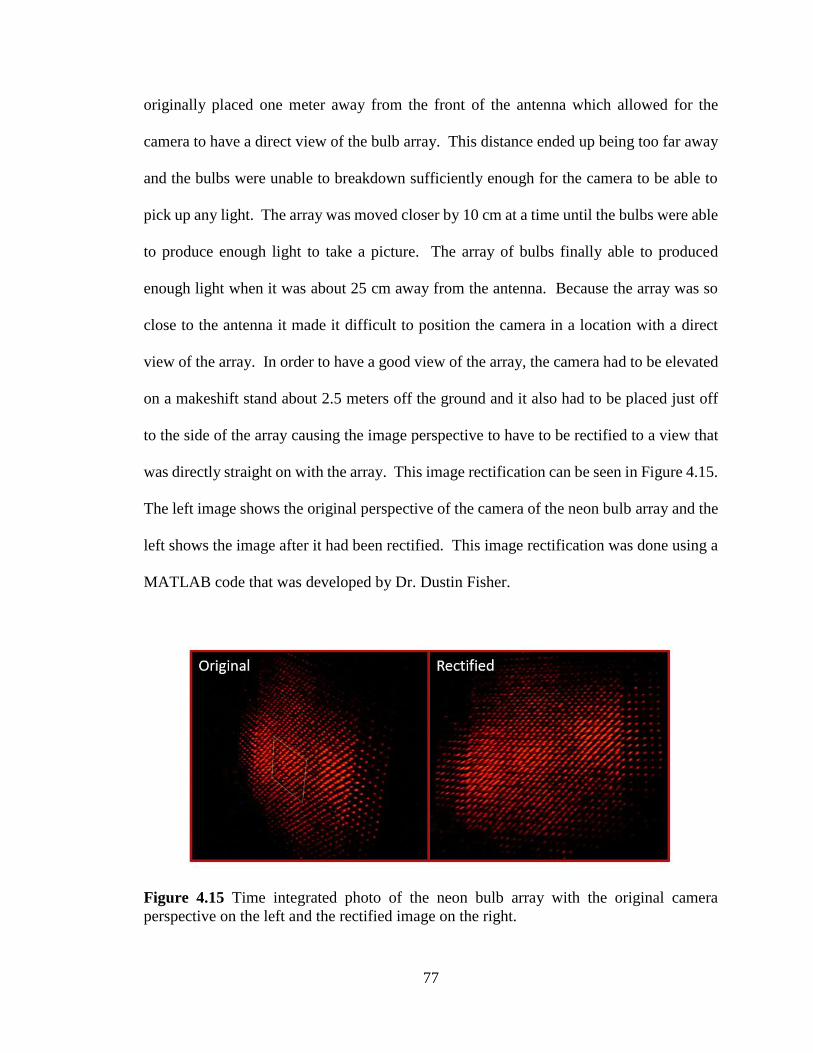
77
originally placed one meter away from the front of the antenna which allowed for the
camera to have a direct view of the bulb array. This distance ended up being too far away
and the bulbs were unable to breakdown sufficiently enough for the camera to be able to
pick up any light. The array was moved closer by 10 cm at a time until the bulbs were able
to produce enough light to take a picture. The array of bulbs finally able to produced
enough light when it was about 25 cm away from the antenna. Because the array was so
close to the antenna it made it difficult to position the camera in a location with a direct
view of the array. In order to have a good view of the array, the camera had to be elevated
on a makeshift stand about 2.5 meters off the ground and it also had to be placed just off
to the side of the array causing the image perspective to have to be rectified to a view that
was directly straight on with the array. This image rectification can be seen in Figure 4.15.
The left image shows the original perspective of the camera of the neon bulb array and the
left shows the image after it had been rectified. This image rectification was done using a
MATLAB code that was developed by Dr. Dustin Fisher.
Figure 4.15 Time integrated photo of the neon bulb array with the original camera
perspective on the left and the rectified image on the right.
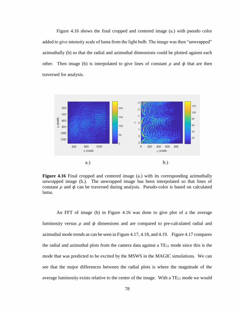
78
Figure 4.16 shows the final cropped and centered image (a.) with pseudo color
added to give intensity scale of luma from the light bulb. The image was then “unwrapped”
azimuthally (b) so that the radial and azimuthal dimensions could be plotted against each
other. Then image (b) is interpolated to give lines of constant 𝜌 and 𝜙 that are then
traversed for analysis.
Figure 4.16 Final cropped and centered image (a.) with its corresponding azimuthally
unwrapped image (b.). The unwrapped image has been interpolated so that lines of
constant 𝜌 and 𝜙 can be traversed during analysis. Pseudo-color is based on calculated
luma.
An FFT of image (b) in Figure 4.16 was done to give plot of a the average
luminosity versus 𝜌 and 𝜙 dimensions and are compared to pre-calculated radial and
azimuthal mode trends as can be seen in Figure 4.17, 4.18, and 4.19. Figure 4.17 compares
the radial and azimuthal plots from the camera data against a TE21 mode since this is the
mode that was predicted to be excited by the MSWS in the MAGIC simulations. We can
see that the major differences between the radial plots is where the magnitude of the
average luminosity exists relative to the center of the image. With a TE21 mode we would
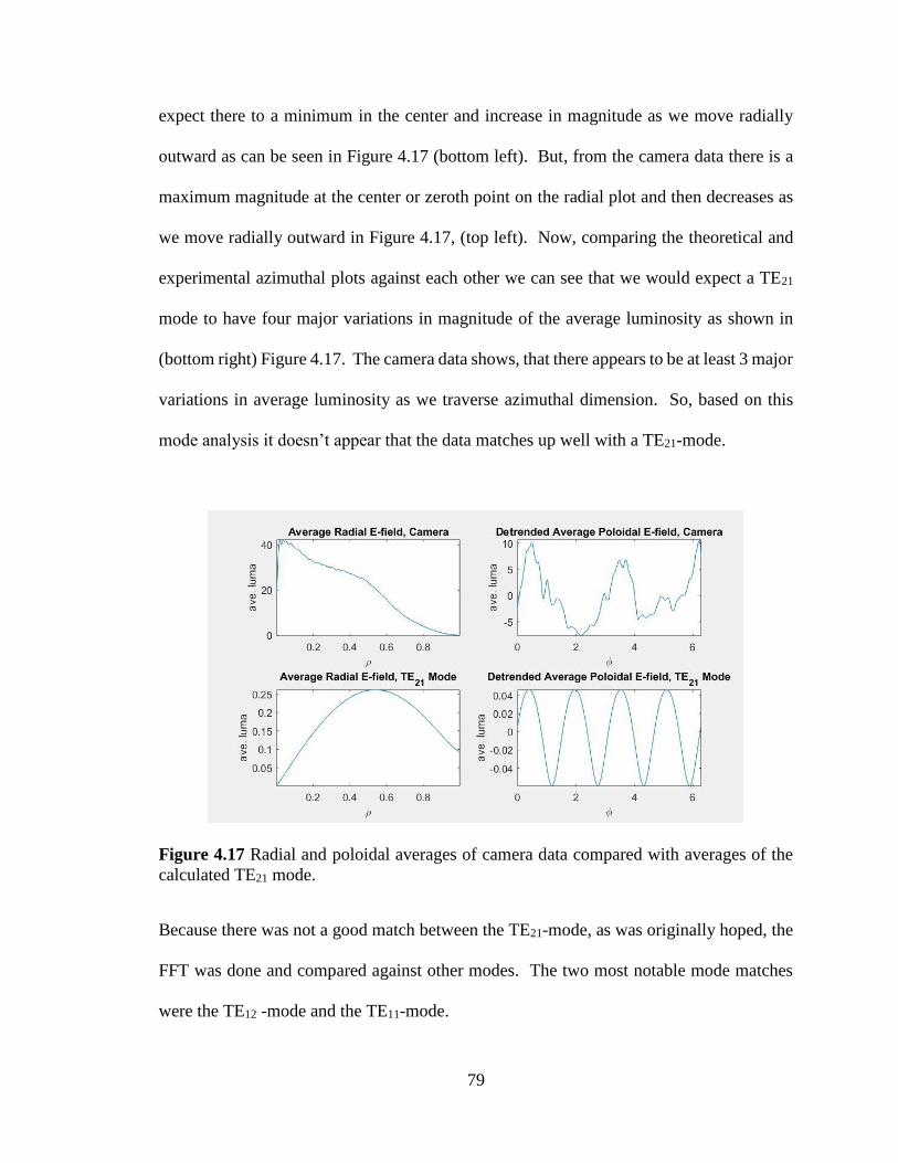
79
expect there to a minimum in the center and increase in magnitude as we move radially
outward as can be seen in Figure 4.17 (bottom left). But, from the camera data there is a
maximum magnitude at the center or zeroth point on the radial plot and then decreases as
we move radially outward in Figure 4.17, (top left). Now, comparing the theoretical and
experimental azimuthal plots against each other we can see that we would expect a TE21
mode to have four major variations in magnitude of the average luminosity as shown in
(bottom right) Figure 4.17. The camera data shows, that there appears to be at least 3 major
variations in average luminosity as we traverse azimuthal dimension. So, based on this
mode analysis it doesn’t appear that the data matches up well with a TE21-mode.
Figure 4.17 Radial and poloidal averages of camera data compared with averages of the
calculated TE21 mode.
Because there was not a good match between the TE21-mode, as was originally hoped, the
FFT was done and compared against other modes. The two most notable mode matches
were the TE12 -mode and the TE11-mode.
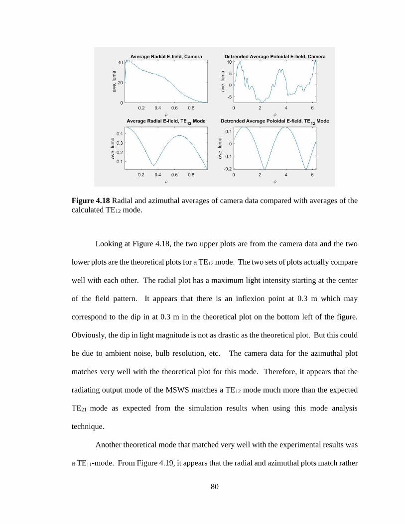
80
Figure 4.18 Radial and azimuthal averages of camera data compared with averages of the
calculated TE12 mode.
Looking at Figure 4.18, the two upper plots are from the camera data and the two
lower plots are the theoretical plots for a TE12 mode. The two sets of plots actually compare
well with each other. The radial plot has a maximum light intensity starting at the center
of the field pattern. It appears that there is an inflexion point at 0.3 m which may
correspond to the dip in at 0.3 m in the theoretical plot on the bottom left of the figure.
Obviously, the dip in light magnitude is not as drastic as the theoretical plot. But this could
be due to ambient noise, bulb resolution, etc. The camera data for the azimuthal plot
matches very well with the theoretical plot for this mode. Therefore, it appears that the
radiating output mode of the MSWS matches a TE12 mode much more than the expected
TE21 mode as expected from the simulation results when using this mode analysis
technique.
Another theoretical mode that matched very well with the experimental results was
a TE11-mode. From Figure 4.19, it appears that the radial and azimuthal plots match rather
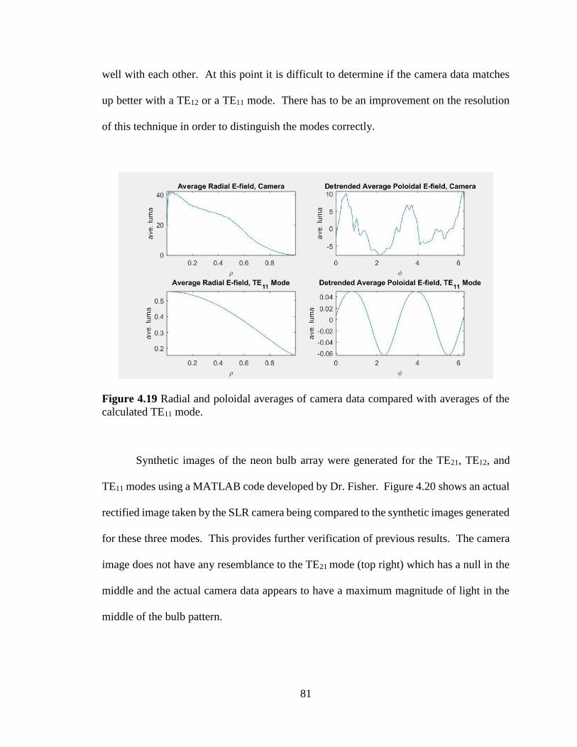
81
well with each other. At this point it is difficult to determine if the camera data matches
up better with a TE12 or a TE11 mode. There has to be an improvement on the resolution
of this technique in order to distinguish the modes correctly.
Figure 4.19 Radial and poloidal averages of camera data compared with averages of the
calculated TE11 mode.
Synthetic images of the neon bulb array were generated for the TE21, TE12, and
TE11 modes using a MATLAB code developed by Dr. Fisher. Figure 4.20 shows an actual
rectified image taken by the SLR camera being compared to the synthetic images generated
for these three modes. This provides further verification of previous results. The camera
image does not have any resemblance to the TE21 mode (top right) which has a null in the
middle and the actual camera data appears to have a maximum magnitude of light in the
middle of the bulb pattern.
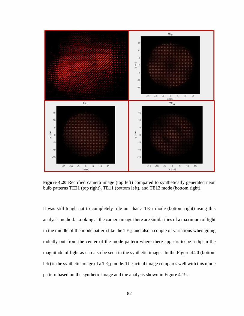
82
Figure 4.20 Rectified camera image (top left) compared to synthetically generated neon
bulb patterns TE21 (top right), TE11 (bottom left), and TE12 mode (bottom right).
It was still tough not to completely rule out that a TE12 mode (bottom right) using this
analysis method. Looking at the camera image there are similarities of a maximum of light
in the middle of the mode pattern like the TE12 and also a couple of variations when going
radially out from the center of the mode pattern where there appears to be a dip in the
magnitude of light as can also be seen in the synthetic image. In the Figure 4.20 (bottom
left) is the synthetic image of a TE11 mode. The actual image compares well with this mode
pattern based on the synthetic image and the analysis shown in Figure 4.19.
83
The data acquired in this experiment does not match a TE21 mode which is expected
to be generated from the MSWS according to the simulation work done by Dr. Yurt and
Dr. Prasad. But the data matches the TE12 and the TE11 modes very well. Finding a way
to increase the resolution with this analysis technique could help with trying to distinguish
between which one of these modes matches up better with the camera data. Also, the
radiation pattern measured (Figures 4.9 and 4.10) have a dip in RF-magnitude at the center
of the radiation pattern which is a characteristic of the TE21 mode and is not what is seen
in the camera data but matches simulation results. One of the major issues why these
experimental results don’t match the simulation results is possibly the board was too close
to the radiating aperture of the antenna and it is possible that this decreased the resolution
enough to give inconclusive results. Another reason could be that there is a change in
boundary conditions at the end of the structure when the RF reaches the coaxial extractor
and then the boundary conditions which maybe acting like a mode converter. Therefore
the mode characterization is inconclusive and further investigation needs to be done to
verify the output mode of the MSWS. One conclusive result is that that the experimental
data and the simulation data both agree that the output mode is a “TE-like” mode and not
a “TM-like” mode. More work needs to be done to figure out what TE mode it actually is.
84
CHAPTER 5: CONCLUSION AND FUTUREWORK
The purpose of this thesis was to extend the experimental work of UNM’s MSWS.
This extension of experimentation included further verification of diode voltage and
current measurements, RF frequency characterization, radiation pattern mapping, detection
of electrical breakdown inside the MSWS, and mode characterization. The average diode
voltage is ≈ 395 kV, the average diode current is ≈ 3.8 kA, giving a diode impedance ≈
104 Ω which agrees well with the MAGIC simulation results. The RF pulse had a pulse-
width of 12 ns, a rise time of 3.2 ns, and a fall time of 8.6 ns. The start time for the RF
generated by the MSWS was about 6 ns into the pulse and agrees well with simulation.
This also suggests that MSWS have a delayed start time before they reach full power. The
frequency of the RF generated by the MSWS was approximately 1.38-GHz which agrees
well with the simulation results with a 4.8% difference between the two. The RF field
pattern shown in Figures 4.9 and 4.10 agree with the HSFF and CST results. The null in
the center of the pattern is a characteristic that coincides with the TE21 mode which was
shown to be the radiating mode in the MAGIC simulation results, provided by Dr. Prasad
and Dr. Yurt. The mode characterization using the neon bulb array and image analysis
showed that the radiating mode of the RF resembled a TE11 mode (see Figure 4.19). This
analysis shows that there is actually a maximum magnitude of electric field intensity at the
center of the mode pattern and decays going towards the edges. This does not correspond
well with the simulation results or radiation pattern which show a null at the center causing
a discrepancy in the results of the mode characterization. There actually could be a lot of
things wrong using the neon bulb array for the mode characterization of MSWS in
85
particular. The main reason being, bulbs weren’t able to breakdown until the array was
25-cm away from the radiating aperture of the antenna. Based on the Eqns. (2.1) and (2.2),
this puts the array in the radiating near-field, and from we learned in chapter 2.1 is that the
mode pattern may not be well formed yet to show its true shape. Another issue was having
to rectify the image at such a large angle due to the array being so close to the antenna that
the view of the SLR camera of the bulbs was pretty steep. Therefore, the rectification
required to put the view into a normal perspective “smeared” some of the image as can be
seen in Figure 4.15 when visually comparing the quality of the original image to the
rectified image. But in conclusion the experimental results of the output mode matches up
rather well with a TE12 and a TE11 modes and the simulation results shows the output mode
is the TE21 mode. Even though these results disagree with one another and are inconclusive
on what the exact mode is being generated, they both agree that the output mode is a TE
mode and not a TM mode. More work needs to be done to see what TE mode it actually
is. On a positive note, there was no electrical breakdown was detected inside of the
MSWS and it survived the harsh HPM environment produced by the SINUS-6. A
diagnostic (MFLD) was developed with a sub-ns response time to detect light emission
from breakdown. It not only can detect the light emission from breakdown, it can localize
it by using multiple channels, and also tell how the breakdown propagates through a system
by comparing the time delays of the signals between the channels. This could be used for
a variety of pulsed power and plasma physics experiments.
Future work will include measuring the radiating power by using an HPM
calorimeter to verify the simulation results as well as determine the overall efficiency of
the MSWS. Improved analysis and characterization of the radiating mode needs to be done

86
because it’s still not clear what the radiating mode of the MSWS is. Additional future
work, would be to try and characterize the light emission from the cathode using
spectroscopy measurements. Having this knowledge could allow for the proper selection
of appropriate filters to be implemented into the collimating lenses of the MFLD. This is
to keep the light from the cathode from saturating out the light emitted from any sources
of electrical breakdown.
87
REFERENCES
[1] J. Benford, J. A. Swegle and E. Schamiloglu, "Introduction," in High Power
Microwaves 3rd Ed., Boca Raton, CRC Press, 2016, pp. 2-15.
[2] E. Schamiloglu, "High Power Microwaves Sources and Applications," in
IEEE MTTS, Fort Worth, 2004.
[3] B. Levush, T. M. Antonsen Jr, A. Bromborsky, W.-R. Lou and Y. Carmel,
"Theory of Relativistic Backward-wave Oscillators with End Reflections,"
IEEE Transactions on Plasma Science, vol. 20, no. 3, pp. 263-280, 1992.
[4] J. Benford, J. A. Swegle and E. Schamiloglu, "BWOs, MWCGs, and O-type
Cerenkov Devices," in High Power Microwaves 3rd Ed., Boca Raton, CRC
Press, 2016, pp. 281-325.
[5] V. Veselago, "The electrodynamics of substances with simultaneously
negative permittivity and permeability," Sov. Physi--Usp, vol. 10, no. 4, pp.
509-514, 1968.
[6] J. B. Pendry, A. J. Holden, D. J. Robbins and W. J. Stewart, "Magnetism
from Conductors and Enhanced Nonlinear Phenomena," IEEE Transaction
on Microwave Theory and Techniques, vol. 47, no. 11, pp. 2075-2084,
1999.

88
[7] D. Smith, D. C. Padilla, S. C. Vier, Nemat-Nasser and S. Schultz,
"Composite medium with simultaneously negatic permeability and
permittivity," Phys. Rev. Lett., vol. 84, pp. 4184-4187, 2000.
[8] R. Marques, J. Martel, F. Mesa and F. Medina, "Left-handed-media
simulation and transmission of EM waves in subwavelength split-ring-
resonator-loaded metallic waveguides.," Physical Review Letters, vol. 89,
no. 18, 2002.
[9] Y. P. Bilokh, S. ev and F. Nori, "Electron beam instability in left-handed
media," Phys. Rev. Lett., vol. 100, no. 4, p. 244803, 2008.
[10] A. Antipov, "Observation of wakefield generation in left-handed band of
metamaterial-loaded waveguide," J. Appl. Phys., vol. 104, no. 1, pp.
014901-1--014901-6, 2008.
[11] D. Shiffler, J. Luginsland, D. M. French and J. Watrous, "A Cerenkov-like
maser based on a metamaterial structure," IEEE Transactions on Plasma
Science, vol. 38, no. 6, pp. 1462-1465, 2010.
[12] M. A. Shapiro, S. Trendafilov, Y. Urzhumoz, A. Alu, R. J. Temkin and G.
Shvets, "Active negative-index metamaterial powered by and electron
beam," Phys. Rev. B., vol. 86, no. 8, p. 085132, 2012.
[13] D. M. French, S. D. and K. Cartwright, "Electron beam coupling to a
metamaterial structure," Phys. Plamsas, vol. 20, no. 8, p. 083116, 2013.

89
[14] J. S. Hummelt, S. M. Lewis, M. A. Shapiro and R. J. Temkin, "Design of a
metamaterial-based backward-wave oscillator," IEEE Transactions on
Plasma Science, vol. 42, no. 4, pp. 930-936, 2014.
[15] S. Prasad, S. Yurt, K. Shipman, D. Andreev, D. Reass, M. Fuks and E.
Schamiloglu, "Compact high-power microwave metamaterial slow-wave
structure: from computational design to hot test validation," IEEE
Transactions on Plasma Science, pp. 61-62, 2017.
[16] S. C. Yurt, "Design of an O-tyoe metamaterial slow wave structure for high
power microwave generation," University of New Mexico, Albuquerque,
2017.
[17] L. Chein-Hao, J. D. Neher, J. H. Booske and N. Behdad, "Investigating the
effective range of vacuum ultraviolet-mediated breakdown in high-power
microwave metamaterials," Journal of Applied Physics, vol. 116, no.
143302, 2014.
[18] J. Benford, J. A. Swegele and E. Schamiloglu, "Microwave Fundamentals,"
in High Power Microwaves 3rd Ed., Boca Raton, CRC Press, 2016, pp. 92-
149.
[19] C. A. Balanis, "Radiation Pattern," in Antenna Theory 3rd Edition,
Hoboken, John Wiley & Sons Inc., 2005, pp. 27-38.
90
[20] J. Lehr and R. Pralhad, "Vacuum," in Foundations of Pulsed Power
Technology, Piscataway, IEEE Press Wiley, 2017, pp. 459-492.
[21] R. Hawley and A. A. Zaky, Progress in Dielectrics, vol. 7, p. 115, 1967.
[22] S. D. Korovin, V. V. Rostov, S. D. Polevin, I. V. Pegel, E. Schamiloglu, M.
I. Fuks and R. J. Barker, "Pulsed Power-Driven High-Power Microwave
Sources," Proceedings of the IEEE, vol. 92, no. 7, pp. 1082-1095, 2004.
[23] High Current Electronics Institute-Tomsk-Russia, "SINUS-6 Repetitively-
Pulsed Electron Beam Accelerator & High Power Microwave Source,"
Tomsk, 1992.
[24] E. Litvinov, "Theory of Explosive Electron Emission," IEEE Transaction of
Electrical Insulation, Vols. EI-20, no. 4, pp. 683-689, 1985.
[25] C. A. Balanis, "Field Regions," in Antenna Theory Analysis and Design 3rd
ed, Hoboken, John Wiley & Sons, Inc., 2005, pp. 34-36.
[26] L. Chien-Hao, J. D. Neher and N. Behad, "Investigating the effective range
of vacuum ultraviolet-mediated breakdown in high-power microwave
metamaterials," Journal of Applied Physics, vol. 116, no. 143302, 2014.
[27] Hamamatsu Photonics, "Photomultiplier Tubes Basics and Applications 3rd
ed," Hamamatsu Photonics, Tokyo, 2007.
[28] Dassault Systemes, "CST Microwave Studio," Waltham.

91
[29] R. Hartley and A. Zisserman, Multiple View Geometry in Compter Vision
2nd Ed., New York: Cambridege University Press, 2003.
[30] P. Kovesi, "MATLAB and Octave Functions for Computer Vision and
Image Processing," [Online]. Available:
http://www.peterkovesi.com/matlabfns/index.html#colour. [Accessed 12
August 2016].
[31] Orbital Atk, "MAGIC 3D," Dulles, 2015.
[32] ANSYS, "High Frequency Electromagnetic Field Simulation," Canonsburg.
[35] Y. Rahmat-Samii, L. I. Williams and R. G. Yoccarino, "The UCLA Bi-polar
PLanar-Near-Field Antenna Measurement and Diagnostics Range," IEEE
Antennas & Propagation Magazine, vol. 37, no. 6, 1995.
[36] Hamamatsu Photonics K.K., Linear Array Multianode PMT Assemblies and
Modules, Shizuoka, 2015.
[37] D. M. Pozar, Microwave Engineering 3rd Ed., Danvers: John Wiley & Sons,
Inc., 2005.


![Electromagnetic Wave Propagation Through Air-Core Waveguide … · medium, or cladding, is made of metamaterial [11-22]. ... Electromagnetic wave propagation through air-core waveguide](https://img.pdfslide.net/doc/110x75/5e779d5da34f2543dc09e5f8/electromagnetic-wave-propagation-through-air-core-waveguide-medium-or-cladding.jpg)