Embed Size (px)
Citation preview
ARTICLE OPEN
Exploring the air stability of PdSe2 via electrical transportmeasurements and defect calculationsAnna N. Hoffman 1, Yiyi Gu1,2, Liangbo Liang3, Jason D. Fowlkes1,3, Kai Xiao3 and Philip D. Rack1,3*
In this work we investigate the effects of ambient exposure on CVD grown PdSe2 and correlate density functional theorycalculations of various physisorption and chemisorption binding energies and band structures to the observed changes in theelectrical transport. Pristine PdSe2 is n-type due to intrinsic selenium vacancies, but shows increased p-type conduction anddecreased n-type conduction as a function of ambient aging during which various aging mechanisms appear to be operative. Shortterm aging (<160 h) is ascribed to an activated chemisorption of molecular O2 at selenium vacancies; first-principles calculationssuggest a ~0.85 eV activation energy and adsorption geometries with binding energies varying between 1.3–1.6 eV, in agreementwith experimental results. Importantly, this chemisorption is reversible with a low temperature anneal. At long term aging (>430 h),there is a total suppression of n-type conduction, which is attributed to a dissociative adsorption/reaction of the O2 molecules toatomic O and subsequent PdO2 formation. XPS confirms the presence of PdO2 in long term aged flakes. At these extended agingtimes, the low temperature anneal restores low n-type conduction and suppresses p-type conduction due to the low thermalstability of PdO2 which, in agreement with XPS measurements, sublimates during the anneal. Thus PdSe2 devices can be processedinto device architectures in standard laboratory environments if atmospheric exposure times are limited to on the order of 1 week.
npj 2D Materials and Applications (2019) 3:50 ; https://doi.org/10.1038/s41699-019-0132-4
INTRODUCTIONThe discovery of atomically thin graphene in 2004 by Novoselovet al. was the catalyst of the 2D materials revolution.1 In layeredmaterials, such as graphene, hexagonal boron nitride (BN), certainoxides and transition metal dichalcogenides (TMDs), weak Van derWaals forces uniquely keep layers bound together,2 and thuspreparation of atomically thin layers is relatively straightforwardvia exfoliation from bulk crystals3–5 or thin film growth.6,7 Due toits chemical structure, each TMD monolayer has an atomicallypristine surface free of dangling bonds and interface traps,8 whichpose a significant issue for silicon and other semiconductor basedmaterials.9 This allows for vertical scaling in advanced devicefabrication with straightforward electrostatics. Processing techni-ques such as defect engineering,10 laser irradiation,11 and plasmaexposure12,13 have been utilized to control material properties andengineer devices with finely tuned properties. Most layered 2Dmaterials have a hexagonal coordination, which promotes atom-ically flat layers. Recently, 2D materials, which have atomsprotruding out-of-plane in a regular corrugated manner, orintralayer “puckering”, have become a focus of research due totheir interesting properties and added degree of freedom.Puckering has been observed in black phosphorus (BP) amongother 2D materials,14 however air stability has been an ongoingchallenge.Palladium diselenide (PdSe2) has recently been identified as a
puckered 2D material, with the additional benefit of a low-symmetry pentagonal structure.15–17 Structurally, each layer isidentical, but there are significant changes in electrical and opticalbehavior as these layers stack due to changes in symmetry andquantum confinement.15,18,19 Additionally, PdSe2 is anticipated tobe electrically anisotropic; mobility should vary depending on thecrystal axis. The most notable and studied layer thickness
dependent effect is the transition from an indirect band gap insome bulk TMD materials to a direct band gap in their monolayercounterpart.18,20 The MoS2 band gap, for instance, varies from~1.2 eV in the bulk to ~1.9 eV at the monolayer, while PdSe2 variesfrom almost no gap (quasi-metallic) to 1.3 eV allowing for uniqueband gap control.15,21 This offers a promising path to logicjunction devices processed in a single material by patterningvarious regions with thicker (contact and resistors) and thinner(semiconductor) regions. While some report PdSe2 to beintrinsically ambipolar,15 as will be demonstrated, we tentativelyattribute this behavior to adsorption at surface chalcogenvacancies and find PdSe2 to be intrinsically n-type due toselenium vacancies.Due to high surface to volume ratio, optoelectronic properties
can be dramatically impacted by atmospheric surface adsorbentsin 2D materials with strong layer number dependence.22–24 Forthis reason it is essential to understand the impact of exposure toambient, which is often unavoidable during fabrication andcharacterization processes, on electrical properties. Electricaleffects of ambient adsorbents and aging have been studied forMoS2
2,23,25–29 and WSe2.22 Studies on MoS2 suggest that ambient
molecules preferentially adsorb to chalcogen surface vacanciesand act as both electron traps and p-type donors.30 While there isnot a consensus on which specific adsorbents contribute toelectron suppression and hole doping, most agree that oxygenproduces the greatest effect. The effects of water adsorption andlong term aging in WSe2 was recently studied and the enhancedp-type conductivity and n-type suppression was associated withelectron transfer to adsorbed water and O2 molecules and areduction of the selenium vacancies, respectively.22 Furthermore,selenides have been shown to be more affected by adsorbedatmospheric species and oxidation effects than sulfides.16,31
1Department of Materials Science & Engineering, University of Tennessee, Knoxville, TN 37996, USA. 2Key Laboratory of Photochemical Conversion and Optoelectronic Materials,Technical Institute of Physics and Chemistry, Chinese Academy of Sciences, Beijing 100190, China. 3Center for Nanophase Materials Sciences, Oak Ridge National Laboratory, OakRidge, TN 37831, USA. *email: [email protected]
www.nature.com/npj2dmaterials
Published in partnership with FCT NOVA with the support of E-MRS
1234567890():,;
Previous studies on 2D materials report significant electricalbehavior variation after a vacuum or inert atmosphere anneal todrive off adsorbed species such as oxygen and water.14,16,32
Bartolomeo et al., recently explored the effects of external stimulisuch as pressure, and optical and electron irradiation on theelectrical properties of exfoliated thick (~25 layer) PdSe2 fieldeffect transistors.33 Notably they observed a transition fromstrongly p-type at atmospheric pressure to ambipolar behaviorwhen pumped to ~1 × 10⁻⁶ Torr. In this work we explore theeffects of short term (90min) ambient exposures and long term(~1000 h) ambient aging and compare atmospheric ambientpressure versus vacuum (~1 × 10⁻⁵ Torr) environmental effects onthe electrical properties of chemical vapor deposition (CVD) grownmultilayer PdSe2; furthermore, we investigate the potential toreverse aging effects through annealing in an inert environment.To rationalize the observed electrical property changes, first-principles density functional theory (DFT) calculations of adsorbedH2O, O2 and O on pristine and Se vacancies in single andmultilayer PdSe2 were performed.
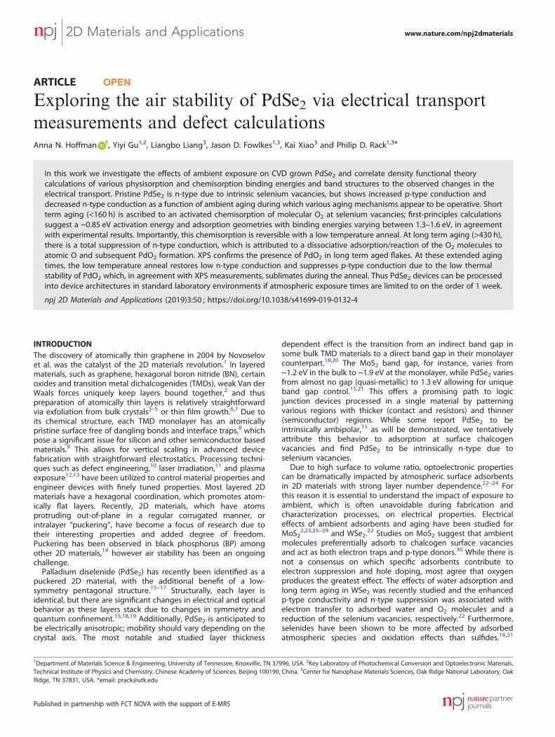
RESULTSTo investigate the effects of short term ambient exposure on theelectrical behavior of PdSe2, a 6 layer PdSe2 FET device wasfabricated. Figure 1a shows an optical micrograph and Fig. 1billustrates a schematic of all devices used in this study. As has beenshown previously, PdSe2 FETs annealed at 177 °C in inert gas for12min show a strong decrease in p-type conduction, increased n-type conduction, and a negative threshold voltage shift.16 Toconfirm this phenomena and investigate the stability of thistreatment, Fig. 1c shows the transfer characteristics of a five-layerPdSe2 device measured in air before a 177 °C anneal and thesubsequent characteristics measured in air as a function of timeafter the anneal. We observe the reported strong n-type increase,p-type decrease, and negative threshold voltage shift; however,over a short ambient exposure time there is a strong reversal ofthese effects. The device shows an increase in the p-typeconduction, a gradual decrease in the n-type conduction, and astrong positive threshold voltage shift toward the pre-anneallevels. It should be noted that there is an approximate 5-min delaybetween the anneal and the first air measurement reported; thus,there is likely some atmospheric exposure effects convoluted inthe initial measurement.
To investigate the effect of ambient pressure on the electricalproperties, Fig. 1d illustrates a series transfer characteristics of a13-layer PdSe2 device measured after the 177 °C anneal at varioustimes during an ~22 h, ~1 × 10⁻⁵ Torr vacuum exposure. It shouldbe noted there is a short period of time (~5min) between theanneal and the vacuum pump down where the device wasexposed to ambient air, first measurement is after 3 min invacuum. Figure 1c, d, both show the annealed samples have adominant n-type conduction which we determine to be thepristine behavior of PdSe2. During the vacuum exposure there is asmall decrease in the p-type conduction, but at the longerexposure time, p-type conduction approaches the original value.Thus this short term effect (<20min) could be due to trappedcharge injection in the underlying SiO2 layer caused during therepetitive forward sweep measurement from −60VGS to +60VGS.
33
The n-type conduction increases over the first 20 min and remainsnearly constant over the next ~22 h. Overall, comparing Fig. 1c, d,dramatic degradation from pristine behavior is observed duringatmospheric exposure, but arrested if device is held in vacuumindicating atmospheric adsorbents are the cause. Conversely,Bartolomeo et al., report strong pressure-dependent conduction inbulk-like exfoliated crystals where they observed reversibleenhanced p-type conduction at atmospheric pressure andenhanced n-type conduction after an extended (10 h) high-vacuum exposure.33 Thus, our study which finds no significantpressure-dependent effects is a bit surprising since, as wasrecently demonstrated in WSe2,
22 thinner flakes are moresusceptible to pressure effects than bulk-like flakes.Subsequent to the initial short term exposure in Fig. 1, a seven-
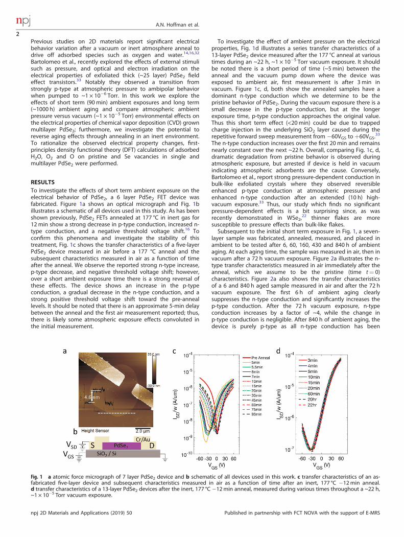
layer sample was fabricated, annealed, measured, and placed inambient to be tested after 6, 60, 160, 430 and 840 h of ambientaging. At each aging time, the sample was measured in air, then invacuum after a 72 h vacuum exposure. Figure 2a illustrates the n-type transfer characteristics measured in air immediately after theanneal, which we assume to be the pristine (time t= 0)characteristics. Figure 2a also shows the transfer characteristicsof a 6 and 840 h aged sample measured in air and after the 72 hvacuum exposure. The first 6 h of ambient aging clearlysuppresses the n-type conduction and significantly increases thep-type conduction. After the 72 h vacuum exposure, n-typeconduction increases by a factor of ~4, while the change inp-type conduction is negligible. After 840 h of ambient aging, thedevice is purely p-type as all n-type conduction has been
Fig. 1 a atomic force micrograph of 7 layer PdSe2 device and b schematic of all devices used in this work. c transfer characteristics of an as-fabricated five-layer device and subsequent characteristics measured in air as a function of time after an inert, 177 °C −12min anneal.d transfer characteristics of a 13-layer PdSe2 devices after the inert, 177 °C −12min anneal, measured during various times throughout a ~22 h,~1 × 10⁻⁵ Torr vacuum exposure.
A.N. Hoffman et al.
2
npj 2D Materials and Applications (2019) 50 Published in partnership with FCT NOVA with the support of E-MRS
1234567890():,;
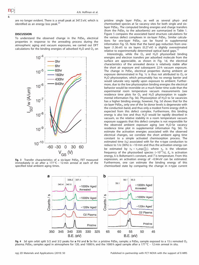
suppressed in our gate voltage range. However, after the 72 hvacuum exposure some n-type conduction is recovered. Interest-ingly, the 840 h aging sample recovers more significantly than the6 h aging sample (as evidenced by the significant thresholdvoltage shift) during the vacuum exposure. As will be discussedbelow, this suggests different aging by-products and in particularthat the 6 h aging byproduct has a higher binding energy than the840 h aging byproduct. Figure 2b, c are plots of the n- and p-typecurrent at ±60 V gate bias versus atmospheric aging time,respectively, measured in air and after the 72 h vacuum exposure(See Fig. S2 for full transfer characteristics). We observe a veryclear increase in the p-type conduction and decrease in the n-typeconduction over this ambient aging time. Comparing the air and72 h vacuum exposure measurements, we observe that thechange in p-type conduction is negligible (decreases by anaverage factor of 1.3) and the n-type conduction increases moresignificantly. For instance, the n-type conduction over the first160 h increases, on average, by a factor of ~5; at 430 and 840 h thedevice displays only p-type conduction in air; however, as shownin Fig. 2a, n-type conduction is recovered after vacuum exposure.Thus, the atmospheric aging appears to have a component that ispartially reversible via room temperature vacuum exposure.A complimentary six-layer PdSe2 FET was fabricated and aged
along with the sample described above, however this sample wasre-annealed prior to each measurement. Figure 3a shows thetransfer characteristics of this sample measured in air immediatelyafter each anneal. (See Fig. S3 for transfer characteristics after a 72h vacuum hold) Clearly the modest aging experienced up to 160 his largely reversible by the anneal, however some residualdegradation to the n-type conduction and enhancement in thep-type conduction remains. Beyond the 160 h measurement, boththe n-type and p-type conduction decreases; thus another agingmechanism emerges between the 160 and 430 h aging, which isconsistent with the dramatic change in the n-type conduction at430 h in Fig. 2c. Recently, Bartolomeo et al.33 studied thehysteresis of multilayer PdSe2 field effect transistors. Theyattributed the observed hysteresis to charge trapping at PdSe2defects and in the near interfacial SiO2 gate region. We also
performed hysteresis measurements for some of the agingconditions after the forward measurements made in Figs. 2aand 3 (see supplemental information Fig. S4 for the hysteresiscurves). In general, our hysteresis data is similar to thosepresented in ref. 33
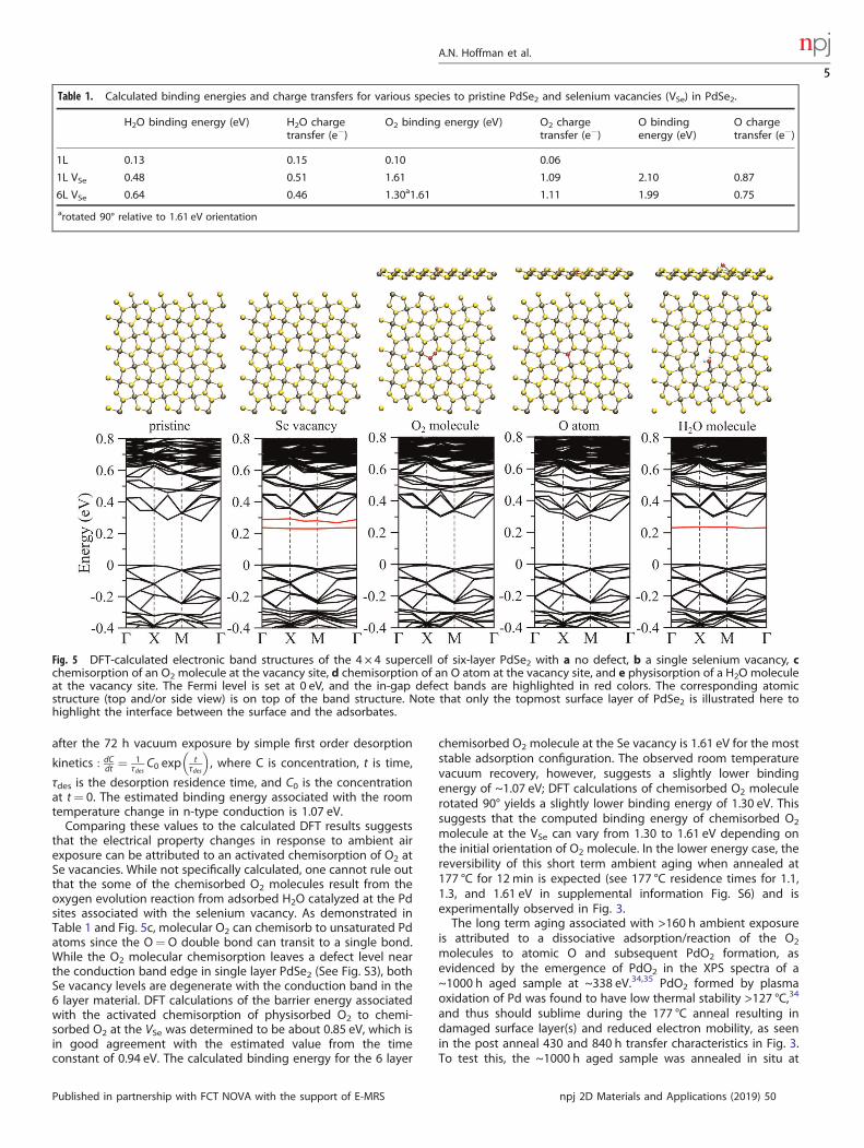
X-ray photoelectron spectroscopy (XPS) spectra were taken on apristine PdSe2 sample, samples that were aged in atmosphere for~120 and ~1000 h, and for reference a PdSe2 sample that wasexposed to a 15 s inductively coupled oxygen plasma exposure.Figure 4 illustrates the 3d spin orbit split 5/2 and 3/2 peaks for 3a,Pd and 3b, Se. Kibis et al. recently studied the thermal and plasmaoxidation of Pd metal and showed that metallic Pd has 3d 5/2peak at 335.2 eV, and the typical PdO (Pd+2) peak is at 337 eV.34
Furthermore, the metastable PdO2 (Pd+4) exhibit a 3d 5/2 at338.2 eV. The pristine PdSe2 (Pd
+4) peak position of the Pd 3d 5/2is at 337.4 eV. This is a lower binding energy relative to PdO2,consistent with Se having a lower electronegativity than O andthus forming a less ionic bond. To confirm the position of thePdO2 peak, we exposed a PdSe2 sample to oxygen plasma undersimilar conditions that were found to oxidize a single layer ofWSe2.
13 The ~120 h aged sample has a small Se–O shoulderemerge at ~59 eV and all Pd and Se peaks are shifted ~0.2 eV tolower energy compared to the pristine sample. This peak shift isconsistent with a Fermi energy shift to toward the valence bandand thus consistent with the observed increase of p-typeconduction. At ~1000 h, the S–O peak is still evident, howevereven more pronounced is the emergence of the PdO2 peaks at~338 (5/2) and 343.4 eV (3/2). The Pd and Se peaks are shifted~0.4 eV to lower energy relative to the pristine sample, which isagain consistent with electrical results which show increased p-type behavior at longer ambient aging times. Consistent with Kibiset al, the plasma oxidized PdO2 3d peaks are ~0.2 eV lower energycompared to the long term ambient aged PdO2 3d peak.34 Kibiset al found the PdO2 oxide from both oxidation methods had lowthermal stability over 127 °C, so to support the claim that PdO2 isforming as PdSe2 samples age in ambient, the ~1000 h agedsample was treated with a 177 °C − 12min anneal in situ andmeasured again. Figure 4 shows that after the anneal, oxide peaks
Fig. 2 a n-type transfer characteristics measured in air immediately after the anneal which we assume to be the pristine (time t= 0)characteristics along with air and post 72 h vacuum exposure characteristics of same device after 6 and 840 h of ambient aging time. b, c plotthe n- and p-type current at ±60 V gate voltage, respectively, versus time in air and after the 72 h vacuum exposure measurements.
A.N. Hoffman et al.
3
Published in partnership with FCT NOVA with the support of E-MRS npj 2D Materials and Applications (2019) 50
are no longer evident. There is a small peak at 347.5 eV, which isidentified as an energy loss peak.34
DISCUSSIONTo understand the observed change in the PdSe2 electricalproperties in response to the annealing process during theatmospheric aging and vacuum exposures, we carried out DFTcalculations for the binding energies of adsorbed H2O and O2 on
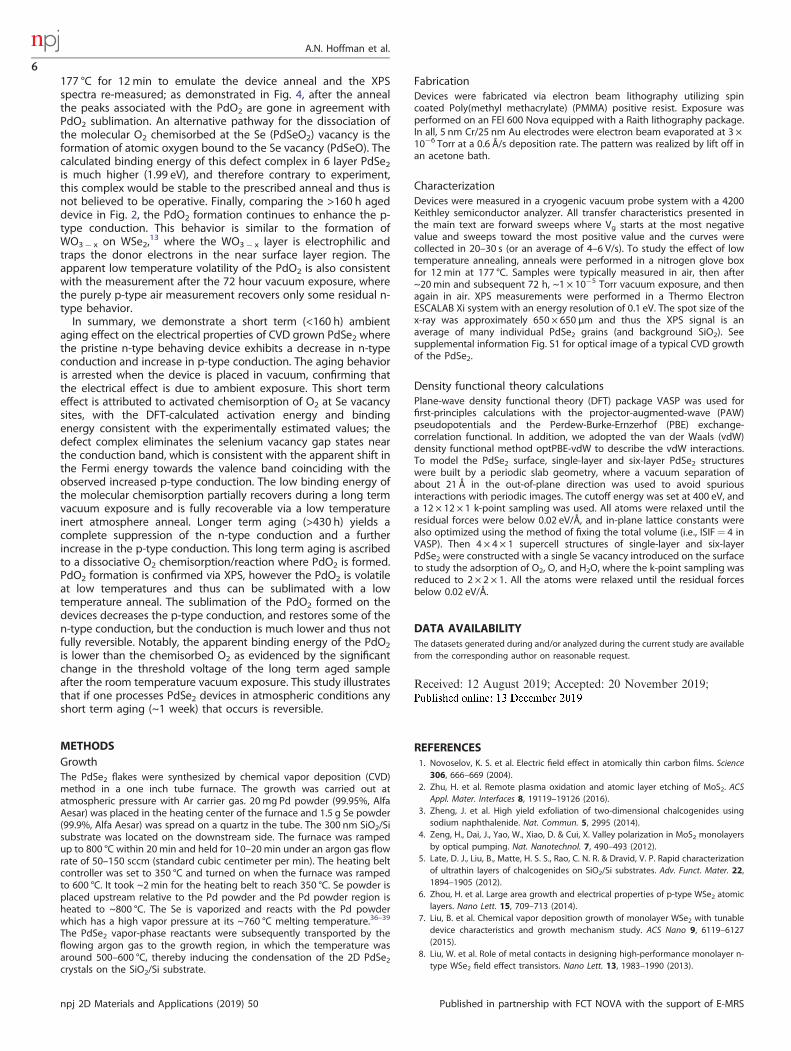
pristine single layer PdSe2 as well as several physi- andchemisorbed species at Se vacancy sites for both single and six-layer PdSe2. The computed binding energies and charge transfers(from the PdSe2 to the adsorbents) are summarized in Table 1.Figure 5 compares the associated band structure calculations forthe various defect complexes in six-layer PdSe2. Similar calcula-tions for one-layer PdSe2 can be found in supplementalinformation Fig. S5. Note that the band gap reduction from one-layer (1.36 eV) to six layers (0.27 eV) is slightly overestimatedrelative to experimentally determined optical band gaps.15
Interestingly, while the O2 and H2O physisorbed bindingenergies and electron transfers per adsorbed molecule from thesurface are appreciable, as shown in Fig. 1d, the electricalcharacteristics of the annealed device is relatively stable afterthe short air exposure and subsequent 22-h vacuum exposure.The change in PdSe2 electrical properties during ambient airexposure demonstrated in Fig. 1c is thus not attributed to O2 orH2O physisorption, which presumably has no energy barrier andwould saturate very rapidly upon exposure to ambient. Further-more, due to the low physisorption binding energies the electricalbehavior would be reversible on a much faster time scale than theexperimental room temperature vacuum measurements (seeresidence time plots for O2 and H2O physisorption in supple-mental information Fig. S6). Physisorption of H2O to Se vacancieshas a higher binding energy, however, Fig. 5d shows that for thesix-layer PdSe2, only one of the Se donor levels is degenerate withthe conduction band, and thus only a modest Fermi energy shift isexpected from this defect complex. Furthermore, this bindingenergy is also low and thus H2O would be rapidly desorbed invacuum, so the relative stability in a room temperature vacuumexposure suggests that this defect complex is not responsible forthe observed ambient exposure aging (see H2O-Se vacancyresidence time plot in supplemental information Fig. S6). Toestimate the activation energies associated with the observedelectrical changes, we correlate the short ambient aging timeconstant to a simple activated chemisorption process. Theestimated time (τR) associated with for the n-type conduction toreduce to 1/e (36%) is ~10min and thus the activation energy canbe estimated by τR ¼ τoexp
EakT
� �; where τo is the vibration
frequency of the physisorbed species (~1013/s), Ea is activationenergy, k is Boltzmann’s constant, and T is temperature. From thisexpression, an activation energy of ~0.94 eV can be estimated.Furthermore, one can estimate the binding energy of thischemisorbed state by comparing the change in n-type current
Fig. 4 3d spin orbit split 5/2 and 3/2 peaks for a Pd and b Se for: a pristine PdSe2 sample; a PdSe2 sample exposed to a 15 s remoted O2plasma; PdSe2 samples aged in atmosphere for 120, and 1000 h; and the 1000 h aged sample after a 177 °C− 12min anneal in situ.
Fig. 3 Transfer characteristics of a six-layer PdSe2 FET measuredimmediately in air after a 177 °C− 12min anneal at each of thespecified total ambient aging times.
A.N. Hoffman et al.
4
npj 2D Materials and Applications (2019) 50 Published in partnership with FCT NOVA with the support of E-MRS
after the 72 h vacuum exposure by simple first order desorption
kinetics : dCdt ¼ 1τdes
C0 exp tτdes
� �, where C is concentration, t is time,
τdes is the desorption residence time, and C0 is the concentrationat t= 0. The estimated binding energy associated with the roomtemperature change in n-type conduction is 1.07 eV.Comparing these values to the calculated DFT results suggests
that the electrical property changes in response to ambient airexposure can be attributed to an activated chemisorption of O2 atSe vacancies. While not specifically calculated, one cannot rule outthat the some of the chemisorbed O2 molecules result from theoxygen evolution reaction from adsorbed H2O catalyzed at the Pdsites associated with the selenium vacancy. As demonstrated inTable 1 and Fig. 5c, molecular O2 can chemisorb to unsaturated Pdatoms since the O=O double bond can transit to a single bond.While the O2 molecular chemisorption leaves a defect level nearthe conduction band edge in single layer PdSe2 (See Fig. S3), bothSe vacancy levels are degenerate with the conduction band in the6 layer material. DFT calculations of the barrier energy associatedwith the activated chemisorption of physisorbed O2 to chemi-sorbed O2 at the VSe was determined to be about 0.85 eV, which isin good agreement with the estimated value from the timeconstant of 0.94 eV. The calculated binding energy for the 6 layer
chemisorbed O2 molecule at the Se vacancy is 1.61 eV for the moststable adsorption configuration. The observed room temperaturevacuum recovery, however, suggests a slightly lower bindingenergy of ~1.07 eV; DFT calculations of chemisorbed O2 moleculerotated 90° yields a slightly lower binding energy of 1.30 eV. Thissuggests that the computed binding energy of chemisorbed O2
molecule at the VSe can vary from 1.30 to 1.61 eV depending onthe initial orientation of O2 molecule. In the lower energy case, thereversibility of this short term ambient aging when annealed at177 °C for 12 min is expected (see 177 °C residence times for 1.1,1.3, and 1.61 eV in supplemental information Fig. S6) and isexperimentally observed in Fig. 3.The long term aging associated with >160 h ambient exposure
is attributed to a dissociative adsorption/reaction of the O2
molecules to atomic O and subsequent PdO2 formation, asevidenced by the emergence of PdO2 in the XPS spectra of a~1000 h aged sample at ~338 eV.34,35 PdO2 formed by plasmaoxidation of Pd was found to have low thermal stability >127 °C,34
and thus should sublime during the 177 °C anneal resulting indamaged surface layer(s) and reduced electron mobility, as seenin the post anneal 430 and 840 h transfer characteristics in Fig. 3.To test this, the ~1000 h aged sample was annealed in situ at
Fig. 5 DFT-calculated electronic band structures of the 4 × 4 supercell of six-layer PdSe2 with a no defect, b a single selenium vacancy, cchemisorption of an O2 molecule at the vacancy site, d chemisorption of an O atom at the vacancy site, and e physisorption of a H2O moleculeat the vacancy site. The Fermi level is set at 0 eV, and the in-gap defect bands are highlighted in red colors. The corresponding atomicstructure (top and/or side view) is on top of the band structure. Note that only the topmost surface layer of PdSe2 is illustrated here tohighlight the interface between the surface and the adsorbates.
Table 1. Calculated binding energies and charge transfers for various species to pristine PdSe2 and selenium vacancies (VSe) in PdSe2.
H2O binding energy (eV) H2O chargetransfer (e−)
O2 binding energy (eV) O2 chargetransfer (e−)
O bindingenergy (eV)
O chargetransfer (e−)
1L 0.13 0.15 0.10 0.06
1L VSe 0.48 0.51 1.61 1.09 2.10 0.87
6L VSe 0.64 0.46 1.30a1.61 1.11 1.99 0.75
arotated 90° relative to 1.61 eV orientation
A.N. Hoffman et al.
5
Published in partnership with FCT NOVA with the support of E-MRS npj 2D Materials and Applications (2019) 50
177 °C for 12 min to emulate the device anneal and the XPSspectra re-measured; as demonstrated in Fig. 4, after the annealthe peaks associated with the PdO2 are gone in agreement withPdO2 sublimation. An alternative pathway for the dissociation ofthe molecular O2 chemisorbed at the Se (PdSeO2) vacancy is theformation of atomic oxygen bound to the Se vacancy (PdSeO). Thecalculated binding energy of this defect complex in 6 layer PdSe2is much higher (1.99 eV), and therefore contrary to experiment,this complex would be stable to the prescribed anneal and thus isnot believed to be operative. Finally, comparing the >160 h ageddevice in Fig. 2, the PdO2 formation continues to enhance the p-type conduction. This behavior is similar to the formation ofWO3− x on WSe2,
13 where the WO3− x layer is electrophilic andtraps the donor electrons in the near surface layer region. Theapparent low temperature volatility of the PdO2 is also consistentwith the measurement after the 72 hour vacuum exposure, wherethe purely p-type air measurement recovers only some residual n-type behavior.In summary, we demonstrate a short term (<160 h) ambient
aging effect on the electrical properties of CVD grown PdSe2 wherethe pristine n-type behaving device exhibits a decrease in n-typeconduction and increase in p-type conduction. The aging behavioris arrested when the device is placed in vacuum, confirming thatthe electrical effect is due to ambient exposure. This short termeffect is attributed to activated chemisorption of O2 at Se vacancysites, with the DFT-calculated activation energy and bindingenergy consistent with the experimentally estimated values; thedefect complex eliminates the selenium vacancy gap states nearthe conduction band, which is consistent with the apparent shift inthe Fermi energy towards the valence band coinciding with theobserved increased p-type conduction. The low binding energy ofthe molecular chemisorption partially recovers during a long termvacuum exposure and is fully recoverable via a low temperatureinert atmosphere anneal. Longer term aging (>430 h) yields acomplete suppression of the n-type conduction and a furtherincrease in the p-type conduction. This long term aging is ascribedto a dissociative O2 chemisorption/reaction where PdO2 is formed.PdO2 formation is confirmed via XPS, however the PdO2 is volatileat low temperatures and thus can be sublimated with a lowtemperature anneal. The sublimation of the PdO2 formed on thedevices decreases the p-type conduction, and restores some of then-type conduction, but the conduction is much lower and thus notfully reversible. Notably, the apparent binding energy of the PdO2
is lower than the chemisorbed O2 as evidenced by the significantchange in the threshold voltage of the long term aged sampleafter the room temperature vacuum exposure. This study illustratesthat if one processes PdSe2 devices in atmospheric conditions anyshort term aging (~1 week) that occurs is reversible.
METHODSGrowthThe PdSe2 flakes were synthesized by chemical vapor deposition (CVD)method in a one inch tube furnace. The growth was carried out atatmospheric pressure with Ar carrier gas. 20 mg Pd powder (99.95%, AlfaAesar) was placed in the heating center of the furnace and 1.5 g Se powder(99.9%, Alfa Aesar) was spread on a quartz in the tube. The 300 nm SiO2/Sisubstrate was located on the downstream side. The furnace was rampedup to 800 °C within 20min and held for 10–20min under an argon gas flowrate of 50–150 sccm (standard cubic centimeter per min). The heating beltcontroller was set to 350 °C and turned on when the furnace was rampedto 600 °C. It took ~2min for the heating belt to reach 350 °C. Se powder isplaced upstream relative to the Pd powder and the Pd powder region isheated to ~800 °C. The Se is vaporized and reacts with the Pd powderwhich has a high vapor pressure at its ~760 °C melting temperature.36–39
The PdSe2 vapor-phase reactants were subsequently transported by theflowing argon gas to the growth region, in which the temperature wasaround 500–600 °C, thereby inducing the condensation of the 2D PdSe2crystals on the SiO2/Si substrate.
FabricationDevices were fabricated via electron beam lithography utilizing spincoated Poly(methyl methacrylate) (PMMA) positive resist. Exposure wasperformed on an FEI 600 Nova equipped with a Raith lithography package.In all, 5 nm Cr/25 nm Au electrodes were electron beam evaporated at 3 ×10⁻⁶ Torr at a 0.6 Å/s deposition rate. The pattern was realized by lift off inan acetone bath.
CharacterizationDevices were measured in a cryogenic vacuum probe system with a 4200Keithley semiconductor analyzer. All transfer characteristics presented inthe main text are forward sweeps where Vg starts at the most negativevalue and sweeps toward the most positive value and the curves werecollected in 20–30 s (or an average of 4–6 V/s). To study the effect of lowtemperature annealing, anneals were performed in a nitrogen glove boxfor 12min at 177 °C. Samples were typically measured in air, then after~20min and subsequent 72 h, ~1 × 10⁻⁵ Torr vacuum exposure, and thenagain in air. XPS measurements were performed in a Thermo ElectronESCALAB Xi system with an energy resolution of 0.1 eV. The spot size of thex-ray was approximately 650 × 650 μm and thus the XPS signal is anaverage of many individual PdSe2 grains (and background SiO2). Seesupplemental information Fig. S1 for optical image of a typical CVD growthof the PdSe2.
Density functional theory calculationsPlane-wave density functional theory (DFT) package VASP was used forfirst-principles calculations with the projector-augmented-wave (PAW)pseudopotentials and the Perdew-Burke-Ernzerhof (PBE) exchange-correlation functional. In addition, we adopted the van der Waals (vdW)density functional method optPBE-vdW to describe the vdW interactions.To model the PdSe2 surface, single-layer and six-layer PdSe2 structureswere built by a periodic slab geometry, where a vacuum separation ofabout 21 Å in the out-of-plane direction was used to avoid spuriousinteractions with periodic images. The cutoff energy was set at 400 eV, anda 12 × 12 × 1 k-point sampling was used. All atoms were relaxed until theresidual forces were below 0.02 eV/Å, and in-plane lattice constants werealso optimized using the method of fixing the total volume (i.e., ISIF= 4 inVASP). Then 4 × 4 × 1 supercell structures of single-layer and six-layerPdSe2 were constructed with a single Se vacancy introduced on the surfaceto study the adsorption of O2, O, and H2O, where the k-point sampling wasreduced to 2 × 2 × 1. All the atoms were relaxed until the residual forcesbelow 0.02 eV/Å.
DATA AVAILABILITYThe datasets generated during and/or analyzed during the current study are availablefrom the corresponding author on reasonable request.
Received: 12 August 2019; Accepted: 20 November 2019;
REFERENCES1. Novoselov, K. S. et al. Electric field effect in atomically thin carbon films. Science
306, 666–669 (2004).2. Zhu, H. et al. Remote plasma oxidation and atomic layer etching of MoS2. ACS
Appl. Mater. Interfaces 8, 19119–19126 (2016).3. Zheng, J. et al. High yield exfoliation of two-dimensional chalcogenides using
sodium naphthalenide. Nat. Commun. 5, 2995 (2014).4. Zeng, H., Dai, J., Yao, W., Xiao, D. & Cui, X. Valley polarization in MoS2 monolayers
by optical pumping. Nat. Nanotechnol. 7, 490–493 (2012).5. Late, D. J., Liu, B., Matte, H. S. S., Rao, C. N. R. & Dravid, V. P. Rapid characterization
of ultrathin layers of chalcogenides on SiO2/Si substrates. Adv. Funct. Mater. 22,1894–1905 (2012).
6. Zhou, H. et al. Large area growth and electrical properties of p-type WSe2 atomiclayers. Nano Lett. 15, 709–713 (2014).
7. Liu, B. et al. Chemical vapor deposition growth of monolayer WSe2 with tunabledevice characteristics and growth mechanism study. ACS Nano 9, 6119–6127(2015).
8. Liu, W. et al. Role of metal contacts in designing high-performance monolayer n-type WSe2 field effect transistors. Nano Lett. 13, 1983–1990 (2013).
A.N. Hoffman et al.
6
npj 2D Materials and Applications (2019) 50 Published in partnership with FCT NOVA with the support of E-MRS
9. Lai, S. K. Interface trap generation in silicon dioxide when electrons are capturedby trapped holes. J. Appl. Phys. 54, 2540–2546 (1983).
10. Stanford, M. G. et al. Focused helium-ion beam irradiation effects on electricaltransport properties of few-layer WSe2: enabling nanoscale direct write homo-junctions. Sci. Rep. 6, 27276 (2016).
11. Stanford, M. G. et al. Purification of nanoscale electron-beam-induced platinumdeposits via a pulsed laser-induced oxidation reaction. ACS Appl. Mater. Interfaces6, 21256–21263 (2014).
12. Stanford, M. G. et al. Lithographically patterned metallic conduction in single-layer MoS2 via plasma processing. npj 2D Mater. Appl. 3, 13 (2019).
13. Hoffman, A. N. et al. Tuning the electrical properties of WSe2 via O2 plasmaoxidation: towards lateral homojunctions. 2D Mater 6, 045024 (2019).
14. Li, L. et al. Black phosphorus field-effect transistors. Nat. Nanotechnol. 9, 372–377(2014).
15. Oyedele, A. D. et al. PdSe2: pentagonal two-dimensional layers with high airstability for electronics. J. Am. Chem. Soc. 139, 14090–14097 (2017).
16. Chow, W. L. et al. High mobility 2D palladium diselenide field-effect transistorswith tunable ambipolar characteristics. Adv. Mater. 29, 1602969 (2017).
17. Puretzky, A. A. et al. Anomalous interlayer vibrations in strongly coupled layeredPdSe2. 2D Mater 5, 035016 (2018).
18. Mak, K. F., Lee, C., Hone, J., Shan, J. & Heinz, T. F. Atomically thin MoS2: a newdirect-gap semiconductor. Phys. Rev. Lett. 105, 136805 (2010).
19. Lee, C. et al. Anomalous lattice vibrations of single-and few-layer MoS2. ACS Nano4, 2695–2700 (2010).
20. Zhao, W. et al. Lattice dynamics in mono-and few-layer sheets of WS2 and WSe2.Nanoscale 5, 9677–9683 (2013).
21. Nguyen, G. D. et al. 3D imaging and manipulation of subsurface seleniumvacancies in PdSe2. Phys. Rev. Lett. 121, 086101 (2018).
22. Hoffman, A. N. et al. Atmospheric and long-term aging effects on the electricalproperties of variable thickness WSe2 transistors. ACS Appl. Mater. Interfaces 10,36540–36548 (2018).
23. Park, W. et al. Oxygen environmental and passivation effects on molybdenumdisulfide field effect transistors. Nanotechnology 24, 095202 (2013).
24. Zhao, P. et al. Air stable p-doping of WSe2 by covalent functionalization. ACSNano 8, 10808–10814 (2014).
25. Giannazzo, F. et al. Ambipolar MoS2 transistors by nanoscale tailoring of schottkybarrier using oxygen plasma functionalization. ACS Appl. Mater. Interfaces 9,23164–23174 (2017).
26. Nan, H. et al. Strong photoluminescence enhancement of MoS2 through defectengineering and oxygen bonding. ACS Nano 8, 5738–5745 (2014).
27. Walter, T. N., Kwok, F., Simchi, H., Aldosari, H. M. & Mohney, S. E. Oxidation andoxidative vapor-phase etching of few-layer MoS2. J. Vac. Sci. Technol. B 35, 021203(2017).
28. Lee, S. Y. et al. Large work function modulation of monolayer MoS2 by ambientgases. ACS Nano 10, 6100–6107 (2016).
29. Qiu, H. et al. Electrical characterization of back-gated bi-layer MoS2 field-effecttransistors and the effect of ambient on their performances. Appl. Phys. Lett. 100,123104 (2012).
30. Ma, D. et al. The role of the intrinsic Se and In vacancies in the interaction of O2
and H2O molecules with the InSe monolayer. Appl. Surf. Sci. 434, 215–227(2018).
31. Jaegermann, W. & Schmeisser, D. Reactivity of layer type transition metal chal-cogenides towards oxidation. Surf. Sci. 165, 143–160 (1986).
32. Ovchinnikov, D., Allain, A., Huang, Y. S., Dumcenco, D. & Kis, A. Electrical transportproperties of single-layer WS2. ACS Nano. 8, 8174 (2014).
33. Di Bartolomeo, A. et al. Pressure-tunable ambipolar conduction and hysteresis inthin palladium diselenide field effect transistors. Adv. Funct. Mater. 29, 1902483,https://doi.org/10.1002/adfm.201902483 (2019).
34. Kibis, L. S., Titkov, A. I., Stadnichenko, A. I., Koscheev, S. V. & Boronin, A. I. X-rayphotoelectron spectroscopy study of Pd oxidation by RF discharge in oxygen.Appl. Surf. Sci. 255, 9428 (2009).
35. Lupan, O. et al. PdO/PdO2 functionalized ZnO:Pd films for lower operatingtemperature H2 gas sensing. Nanoscale 10, 141107 (2018).
36. Zeng, L.-H. et al. Controlled synthesis of 2D palladium diselenide forsensitive photodetector applications. Adv. Funct. Mater. 29, 1806878(2019).
37. Wu, D. et al. Highly polarization-sensitive, broadband, self-powered photo-detector based on graphene/PdSe2/Germanium heterojunction. ACS Nano 13,9907–9917 (2019).
38. Luo, L. et al. PdSe2 multilayer on germanium nanocones array with light trappingeffect for sensitive infrared photodetector and image sensing application. Adv.Funct. Mater. 29, 1900849 (2019).
39. Okamoto, H. The Pd-Se (palladium-selenium) system. J. Phase Equilibria 13, 69–72(1992).
ACKNOWLEDGEMENTSP.D.R., A.N.H., J.D.F and L.L. acknowledge support from the US Department of Energy(DOE) under grant number KC 0403040 ERKCZ01. A.N.H. also acknowledges supportfrom the Center for Materials Processing. Y.G. and K.X. acknowledge support by theU.S. Department of Energy, Office of Science, Basic Energy Sciences, MaterialsSciences and Engineering Division. Material growth, device synthesis, DFT calculations,and characterization measurements were conducted at the Center for NanophaseMaterials Sciences, which is a DOE Office of Science User Facility. P.D.R. and A.N.H.would like to acknowledge Jonathan Woodward and Harry Meyer for help acquiringthe XPS data.
AUTHOR CONTRIBUTIONSP.D.R. conceived of the experimental plan and managed the project. A.N.H.performed the device fabrication and electrical characterization. Y.G. and K.X. grew2D PdSe2 crystals; Y.G. performed AFM measurements; A.N.H. with assistance fromJonathan Woodward and Harry Meyer performed X.P.S. measurements; L.L. did theDFT calculations; J.D.F. developed residence time plots. The paper was writtenthrough contributions of all authors. All authors have given approval to the finalversion of the paper.
COMPETING INTERESTSThe authors declare no competing interests.
ADDITIONAL INFORMATIONSupplementary information is available for this paper at https://doi.org/10.1038/s41699-019-0132-4.
Correspondence and requests for materials should be addressed to P.D.R.
Reprints and permission information is available at http://www.nature.com/reprints
Publisher’s note Springer Nature remains neutral with regard to jurisdictional claimsin published maps and institutional affiliations.
Open Access This article is licensed under a Creative CommonsAttribution 4.0 International License, which permits use, sharing,
adaptation, distribution and reproduction in anymedium or format, as long as you giveappropriate credit to the original author(s) and the source, provide a link to the CreativeCommons license, and indicate if changes were made. The images or other third partymaterial in this article are included in the article’s Creative Commons license, unlessindicated otherwise in a credit line to the material. If material is not included in thearticle’s Creative Commons license and your intended use is not permitted by statutoryregulation or exceeds the permitted use, you will need to obtain permission directlyfrom the copyright holder. To view a copy of this license, visit http://creativecommons.org/licenses/by/4.0/.
© The Author(s) 2019
A.N. Hoffman et al.
7
Published in partnership with FCT NOVA with the support of E-MRS npj 2D Materials and Applications (2019) 50

![Van der Waals PdSe2/WS2 Heterostructures for Robust High ... Braodband PDs.pdffor the spectrum of PdSe ‘ film.[‡, …a] When it comes to Raman spectrum of PdSe ‘/WS ‘ heterostructure](https://img.pdfslide.net/doc/110x75/610d08ec7b322f2aab52be63/van-der-waals-pdse2ws2-heterostructures-for-robust-high-braodband-pdspdf-for.jpg)


![1 TCP Libra: Exploring RTT-Fairness for TCPcheung/Courses/558/Syllabus/... · Massoulie, Johari and Tan addressed the stability in network congestion control schemes [18]. Vinnicombe](https://img.pdfslide.net/doc/110x75/600d3e2c4db9b872512b3b02/1-tcp-libra-exploring-rtt-fairness-for-cheungcourses558syllabus-massoulie.jpg)