Embed Size (px)
Citation preview

EXPLORING THE NANOLANDSCAPE
Nanometer-scale Science and Technology
using Scanning Probe Microscopy
Professor N. John DiNardoDepartment of Physics
Drexel University

N. John DiNardo, 2001
Page 2 of 35

NANOSCIENCE AND TECHNOLOGY - A Brief Introduction
Nanotechnology represents a scientific and engineering frontier that is currently being vigorously explored throughout the world by leading scientists and engineers in academia, national laboratories, and industry. The term "nano", or nanoscale, refers to the structural sizes of interest – the nanometer (nm), or 10-9 meter. With a representative atomic diameter of ~0.2 nm, nano-science/technology addresses objects as small as a few atomic diameters in at least one dimension up to ~100 nm. The "micro"-meter (10-6 meter) size regime extends beyond the nanoscale, and often there is considerable overlap. The ultimate goal of nanotechnology is to fabricate and utilize the unique functional properties of nanostructures, as scientists and engineers have been doing in microelectronics for many years.
Why is this size scale so important? Let us consider two vastly different cases – microelectronics and biochemistry. It has been widely recognized for years that smaller electronic circuit features in integrated circuits has increased the computing power of microprocessors. Integrated circuit fabrication is an example of a system that is built "top-down," that is, features are etched into (large) bulk materials, having been defined by optical lithography. Unfortunately, feature sizes cannot be made much smaller than optical wavelengths, so that continued miniaturization requires new approaches. In the top-down approach for integrated circuit fabrication, short-wavelength x-ray or electron beam lithography are possibilities. It is recognized that biological macromolecules, the building blocks of life, are complex arrangements of atoms forming nanoscale structures. Assembling different types of macromolecules into micron-scale cells produce chemical engines capable of replication. In understanding and controlling basic functions of macromolecules, biochemists are creating new drugs that target specific diseases and diseased tissues. The assembly of biological structures occurs by reactions and aggregations of atoms and molecules, a "bottom-up" process. Trying to mimic such processes for various applications – from microelectronics to biochemistry – suggests that ultimate control at the single atom level could be very important.
A physicist would claim that physics forms the basis of chemistry, biology, and materials science. While this might be true, it must be recognized that theoretically describing a complex macromolecule on the basis of the interactions of individual atoms is not yet possible; it is rather necessary to understand physical interactions and processes of complex aggregates whose properties are already understood at a certain level. Similarly, the ability to measure various parameters of molecular systems – structurally, spectroscopically, thermally, etc. – relies on processes that can be described by specific physical interactions.
Page 3 of 35
Let us focus on the smallest entity under discussion – the atom. (While elementary particles comprise the structures that make up an atom, the association of electronic states of the atom lead to chemical bonding, and the energy scales associated with these electronic states are common to chemical and solid-state materials processes.) Much effort in nanoscience and nanotechnology is directed at understanding materials and materials processes as atomic assemblies. For example, can one create a thin wire that just one row of atoms wide? As is often the case, one is tempted to scale down one's everyday experience from the macroscopic world, i.e., large assemblies of atoms that can be considered as continuous media. While valid in many cases, it is striking that when things become small, materials behave in new ways. One reason is because the quantum mechanical description that applies to the behavior of electrons must be considered in detail when an electron is confined with a very small structure, such as an atomic wire or a nanosphere or an atomically-abrupt interface. This is because the electrons in quantum mechanics are treated as waves; when the electron wavelength, related to its energy, is of the same order as the size of the container, e.g., the nanosphere, a discrete (rather than a quasi-continuous) energy spectrum arises. It should be noted that spectroscopic measurements in chemistry represent the quantum nature of the ensemble of discrete atoms or molecules. Another reason for reconsidering the description relates to the increased importance of surfaces for small objects; very simply, the surface-to-volume ratio becomes much larger. Interactions between surfaces, such as adhesion effects or frictional effects, become more important.
Returning to the goals of nanoscience and nanotechnology, it is apparent that scientists and engineers might want to ultimately achieve control of single atoms to make new things (electronic circuits, machinery, chemicals, etc.) while recognizing that the physical properties of such things might be quite unique. Thus, the "scaled-down view" is not necessarily correct. It will hopefully become apparent that we are just beginning to understand matter at this level – and that understanding must precede application in most cases. Experience does in fact suggest how such understanding and application might be achieved. We would like to visualize, measure and manipulate matter at the atomic level as we do larger objects with our eyes, our other senses, and our hands. In any discussion of nanotechnology, Scanning Probe Microscopies, a host of techniques that have opened the door to the possibilities of not only microscopy but also of spatially-localized measurement and manipulation, is highlighted because of these unique capabilities.
The goal of this article is to describe the fundamental capabilities of Scanning Probe Microscopies (SPM) from the point of view of a physicist with obvious extensions to other disciplines. The interdisciplinary nature of materials research is even more evident when the importance of the nanoscale is recognized. Developing new materials is clearly the driving force
Page 4 of 35

for progress in most engineering disciplines. SPM addresses several fundamental physical phenomena, such as electron tunneling and electron transport through confined regions, the measurement of atomic structure and atom diffusion on surfaces, spatially-localized surface spectroscopy, surface modification on the atomic scale and quantum confinement, atomic forces, the nanoscale basis for friction, surface elasticity, and surface magnetism. These phenomena are fundamental to applications and processes in Chemistry, Biology, and Engineering. The most obvious applications are in Materials Engineering where imaging with atomic resolution permits detailed characterization of new materials. Beyond characterization, the prospect of building new materials one atom at a time – not necessarily in a production environment but for fundamental studies – is very exciting. In Electrical Engineering, there is great interest in the quantum nature of microscopic phenomena, such as electrical conductivity, as well as in information storage – modifying and accessing information on the atomic scale represents the highest information storage density one can imagine. In Chemistry and Chemical Engineering, understanding chemical specificity at surfaces and engineering surface reactivity can lead to controlling processes at the nanometer scale. In Mechanical Engineering, understanding friction on the atomic scale, in Civil Engineering, the interaction of coatings on surfaces, and in Biomedical Engineering / Engineering Biomaterials the structure and mechanisms of biological systems such as protein structure and protein folding forces can be explored.
To close this section, it is fair to assert that nanotechnology captures the imaginations of people in many walks of life. In fact, a futuristic vision of the potential of nanotechnology, as described by Richard Feynman in December 1959 (Feynman 1959), is remarkably true to some of the capabilities that are being demonstrated today. Other futuristic visions of nanotechnology by K. Eric Drexler (Drexler 1990) and others test the realm of science fiction but might not be so unbelievable in the foreseeable future.
SCANNING PROBE MICROSCOPY
Some of the most dramatic pictures in the recent technological literature are false-color (or greyscale) images of individual atoms, molecules, and macromolecules, such as that of iron atoms arranged in a circle on a copper surface shown in Figure 1, that have been obtained by Scanning Probe Microscopes (SPMs) (DiNardo 1994). While imaging atoms with SPM is itself a great accomplishment, SPMs, with effective probe dimensions that can be smaller than the size of an atom and with control of sub-nanometer precision, can also probe, or interrogate, highly localized physical properties on top of atoms or groups of atoms. With various techniques and in specific data acquisition modes, localized electronic spectra, vibrational spectra, and interatomic
Page 5 of 35

bonding forces can be measured. Perhaps it is even more impressive to see images of atoms that have been positioned, or manipulated, by an SPM, the atoms having been translated with the tip to desired locations on various material surfaces to “write” a word, “sketch” a nano-design, or create new electronic states. SPMs have become key analytic tools over less than a twenty year time period since the invention of the Scanning Tunneling Microscope (STM). In this article, we will consider the wide-ranging state-of-the-art capabilities of SPMs by taking examples of interesting images and spectra that have been published. As pictured in Figure 2, feature sizes imaged by SPM range from atomic diameters (~0.3 nm) to those related to advanced microelectronics devices (~0.25 µm) and biological systems such as proteins (~1 µm).
Figure 1: Electron standing waves in a “quantum corral” – an
arrangement of forty-eight iron atoms on a copper surface.
(From: www.almaden.ibm.com/vis/stm)
The topics described in this article represent the basis of nanoscience and nanotechnology. We go beyond “miniaturization” to physical, electronic, and chemical properties and processes based on the atomistic basis of materials properties. We will see the potential of devices constructed of perhaps a few atoms and functioning at a level at which a quantum mechanical description is required for design has been realized and is very important to future technological progress - not just a scientific curiosity. Although we will discuss micron-sized objects in the context of SPM, we will define the nanoscale as ranging from atomic dimensions to 100 nm.
The following is a partial list of topics to be discussed: self-assembly of polymer films based on latex particles – from ordered assemblies to
continuous films crystalline surfaces of materials imaged at the atomic scale – imaging atomic
structure inferred from images of localized electronic states spectroscopy of single atoms and molecules on surfaces – mapping wavefunctions (or
orbitals)
Page 6 of 35

measuring atoms diffusing along a surface – leading to the formation of crystalline layers
viewing the structure and the operation of microelectronics circuits – observations of electrostatic potentials in a device
electrons confined in artificial nanostructures – creating new electronic states due to quantum confinement
wires of single atomic diameter thickness – observing quantized conductance when the narrowest of "wires"
mechanical and electronic properties of carbon nanotubes assembled to create nanocircuits – observing properties of a new class of "building blocks"
measuring bonding forces in biological macromolecules – directly measuring bonding and electrostatic forces in a move towards nanobiotechnology
a b c
Figure 2: (a) Atomic-resolution image of Cu(111) at a temperature of 105 K (from E. Wahlström, I.
Ekvall, H. Olin and L. Wallden at Chalmers University of Technology posted at www.omicron-
instruments.com (b) A 5 m scan of an integrated circuit wafer. From www.di.com. (c) SFM image of the
protein fibronectin attached to a nanostructured titanium thin film.
The atom is the building block of a material. Crystalline solids are composed of regular arrays of atoms that form distinct bulk crystal structures based on details of the interatomic interaction energies. A cubic unit cell (the volume representing the repeat structure of the crystal) is typically about 0.3 nm on a side as shown in Figure 3. With one atom per unit cell, 1 cm3 contains ~4 1022 atoms. While three-dimensional solids make up most structures, our access to the material is through the surface. By access, we mean what we touch, where we make electrical contact, where we join materials, what we see, etc. Therefore the surface and interfacial properties of materials are very important and encompass the field called Surface Science. In a simplest picture, the surface is the uppermost layer(s) of atoms of a solid. Using the numbers above, we estimate that there are ~1 1015 surface atoms per square centimeter. As we will note later, the surface atoms might change positions (with respect to their bulk positions) due to the fact that they no longer “feel” nearest-neighbor atoms all around them. Also, these surface atoms are likely to interact chemically with the surrounding atmosphere, for example the
Page 7 of 35

surface of a metal might oxidize or the surface might catalyze a chemical reaction. We will consider in many examples atomically clean surfaces that can be prepared and maintained in a very good vacuum. Joining two materials means creating an interface. For nanotechnology, we might consider a thin film that is grown on a clean surface by evaporation or by adsorption by exposing the surface to a gas or a liquid.
Figure 3: The cesium chloride crystal
structure which is 4.11 Å on a side.
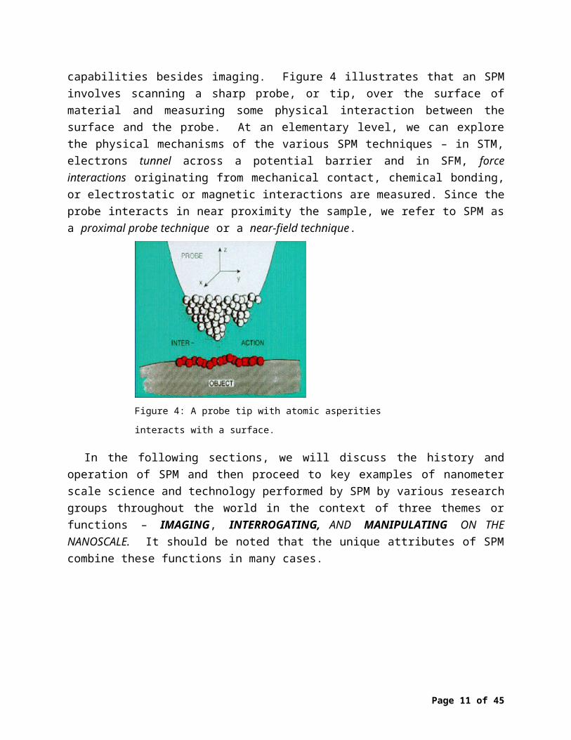
We are familiar with viewing small structures by optical microscopy; however, the resolution is only the order of a wavelength of visible light, hundreds of nanometers. Electron microscopy offers the ability to get to atomic dimensions; for example, the wavelength of an electron accelerated across a potential difference of ~10 kV is ~0.01 nm. With proper stability, an electron microscope can see atomic structure in reflection and in transmission. Alternatively, SPM allows other capabilities besides imaging. Figure 4 illustrates that an SPM involves scanning a sharp probe, or tip, over the surface of material and measuring some physical interaction between the surface and the probe. At an elementary level, we can explore the physical mechanisms of the various SPM techniques – in STM, electrons tunnel across a potential barrier and in SFM, force interactions originating from mechanical contact, chemical bonding, or electrostatic or magnetic interactions are measured. Since the probe interacts in near proximity the sample, we refer to SPM as a proximal probe technique or a near-field technique.
Page 8 of 35

Figure 4: A probe tip with atomic asperities interacts with a surface.
In the following sections, we will discuss the history and operation of SPM and then proceed to key examples of nanometer scale science and technology performed by SPM by various research groups throughout the world in the context of three themes or functions – IMAGING, INTERROGATING, AND MANIPULATING ON THE NANOSCALE. It should be noted that the unique attributes of SPM combine these functions in many cases.
Page 9 of 35

HISTORY
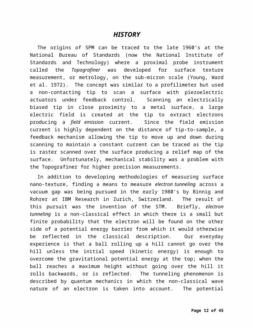
The origins of SPM can be traced to the late 1960’s at the National Bureau of Standards (now the National Institute of Standards and Technology) where a proximal probe instrument called the Topografiner was developed for surface texture measurement, or metrology, on the sub-micron scale (Young, Ward et al. 1972). The concept was similar to a profilimeter but used a non-contacting tip to scan a surface with piezoelectric actuators under feedback control. Scanning an electrically biased tip in close proximity to a metal surface, a large electric field is created at the tip to extract electrons producing a field emission current. Since the field emission current is highly dependent on the distance of tip-to-sample, a feedback mechanism allowing the tip to move up and down during scanning to maintain a constant current can be traced as the tip is raster scanned over the surface producing a relief map of the surface. Unfortunately, mechanical stability was a problem with the Topografiner for higher precision measurements.
In addition to developing methodologies of measuring surface nano-texture, finding a means to measure electron tunneling across a vacuum gap was being pursued in the early 1980’s by Binnig and Rohrer at IBM Research in Zurich, Switzerland. The result of this pursuit was the invention of the STM. Briefly, electron tunneling is a non-classical effect in which there is a small but finite probability that the electron will be found on the other side of a potential energy barrier from which it would otherwise be reflected in the classical description. Our everyday experience is that a ball rolling up a hill cannot go over the hill unless the initial speed (kinetic energy) is enough to overcome the gravitational potential energy at the top; when the ball reaches a maximum height without going over the hill it rolls backwards, or is reflected. The tunneling phenomenon is described by quantum mechanics in which the non-classical wave nature of an electron is taken into account. The potential barrier at the surface of a material is called the work function and is created by the electrostatic potential set up due to the truncation of the bulk atomic structure. When the tip and sample are near each other, a narrow barrier is set up from the overlap of the work function barriers of the tip and sample. When the tip is biased positive with respect to the sample by a power supply, electrons flow, or tunnel, to the unoccupied states of the tip.
The design and function of the STM was remarkably similar to that of the Topografiner. In the seminal paper appearing in Applied Physics Letters, the first observation of electron tunneling across a stable vacuum gap for several different tip-sample biases was reported (Binnig, Rohrer et al. 1982). Vibrational stability was obtained by mounting the STM on a magnetically levitated platform. A tungsten tip mounted on a piezoelectric transducer and coarse approach stage was used to approach a platinum surface, and the exponential dependence of
Page 10 of 35
current vs. gap separation over four orders of magnitude was observed with a barrier height consistent with vacuum tunneling. Shortly thereafter, Binnig and Rohrer demonstrated that surface atomic structure could be imaged by STM, with the first atom-resolved images of a silicon surface, the so-called Si(111)-77 reconstructed surface (Binnig et al., 1983). The remarkable ability to obtain atomic resolution is attributed to the strong dependence on height and the frontier protrusion of a single atom from the metal tip.
Figure 5: A semi-log plot of current vs. tip-surface separation
shows exponential behavior characteristic of electron tunneling.
From (Binnig, Rohrer et al. 1982).
Shortly thereafter, Binnig and Quate introduced the SFM, or Atomic Force Microscope (AFM), and demonstrated the ability to obtain surface structural information by monitoring the movement of a sharp tip mounted on a foil that acted as a cantilever placed in contact with a surface (Binnig, Quate et al. 1986). At that time, the small vertical displacements of the cantilever were detected with an STM tip. Correlation of the displacement of the cantilever with force led the inventors to predict forces smaller than a piconewton could be measured with this technology.
Many companies have begun producing SPMs over the last ten years. While the basic instrument remains the same, intense research continues on new measurement approaches and new applications for the instrumentation.
HOW DOES SPM WORK?
STM images are obtained either by maintaining a constant tunneling current as the feedback circuit allows the tip to move up or down to stay at a constant height above the surface or by
Page 11 of 35
maintaining a constant height and measuring current variations because of changes in the tunneling gap.
Figure 6 Figure 7
Figure 6: Schematic of electron tunneling, including electronic states, from a biased tip and
surfaces. From (Hamers, Tromp et al. 1986).
Figure 7: An Omicron ultrahigh vacuum scanning tunneling microscope.
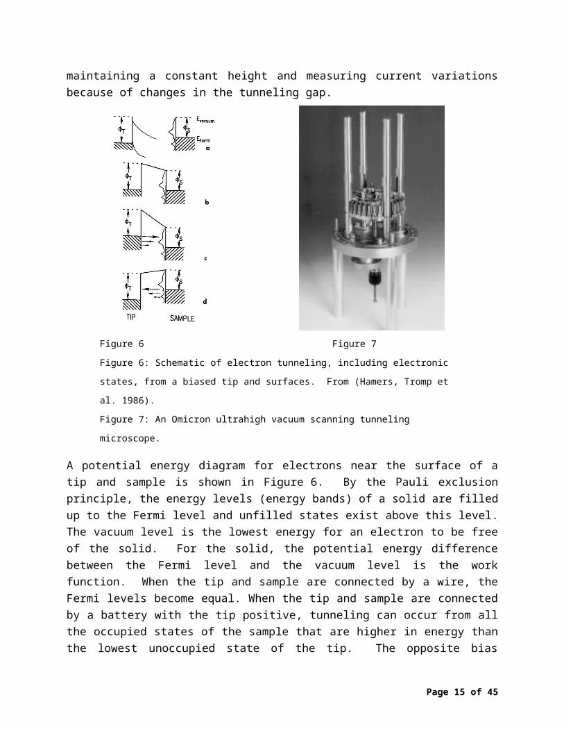
A potential energy diagram for electrons near the surface of a tip and sample is shown in Figure 6. By the Pauli exclusion principle, the energy levels (energy bands) of a solid are filled up to the Fermi level and unfilled states exist above this level. The vacuum level is the lowest energy for an electron to be free of the solid. For the solid, the potential energy difference between the Fermi level and the vacuum level is the work function. When the tip and sample are connected by a wire, the Fermi levels become equal. When the tip and sample are connected by a battery with the tip positive, tunneling can occur from all the occupied states of the sample that are higher in energy than the lowest unoccupied state of the tip. The opposite bias permits tunneling from tip to sample. The tunneling probability is governed by the height and width of the barrier, which must be very thin to obtain any appreciable tunneling current. The tunneling current exhibits an exponential dependence on the tip-sample separation, d. The tunneling probability (or the tunneling current) is proportional to e-2d, where ~ 1 Å-1 for a potential energy barrier ~4 eV high. The current is of the order of 1 nA for a gap, d ≈ 1 nm. It is important to note that the strong exponential dependence causes the tunneling current to be reduced by a factor of ~10 for every 1 Å increase in the gap distance. Again, this indicates that
Page 12 of 35

the tunneling current can be localized to the frontier atom at the tip apex. Going one step further, it is known that energies of the electronic states of the solid and any adsorbed species actually contain more detail as indicated in Figure 6(c),(d) by peaks in the so-called density of states. Changing the tunneling bias tunes these states in and out, so the electronic (and/or vibrational) spectrum of a localized region can also be probed. As a corollary, it is apparent that the image obtained with an STM is really an image of the accessible electronic states at the particular bias for which the image is acquired. Maintaining a stable tunnel junction with an accuracy of <0.1 nm as the tip is scanned over the surface is the most crucial aspect of STM operation and therefore demands that the apparatus exhibit high mechanical stability. In addition, since the tip and sample are typically mounted at points much larger than the tip-sample separation, thermal drift must be compensated and a high degree of vibration/shock isolation must be ensured. The STM head is typically designed to meet the criteria of the measurements which are to be performed, e.g. constant temperature vs. variable temperature, atomic resolution vs. wide scan range. The first step to meet these goals is to design a rigid structure in the STM head keeping uniformity of thermal expansion coefficients in the materials used. This provides the apparatus with a high resonance frequency aiding in isolating vibrations from the surroundings; uniform materials provide good thermal drift characteristics. Obviously, tip structure and preparation is important to obtain atomic resolution images, and several recipes have been developed and tested. One of the key technical problems in operating an STM is the coarse approach allowing the tip-sample separation to proceed from macroscopic distances to the tunneling regime. This aspect largely dictates the microscope design, being handled successfully in a number of ways – purely mechanically or electro-mechanically. Microactuation of the probe tip is typically accomplished using piezoelectric transducers for motion in each of the three orthogonal directions. The control electronics incorporates low-noise current pre-amplification, and, in the constant current mode, tunnel current feedback controls the height of the tip by adjusting the z-piezoelectric element as the tip is rastered in the (x,y) plane. Scanning the tip, setting or scanning the tip-sample bias, and other data acquisition tasks are performed in real-time by a microcomputer while image analysis and processing can be performed by the same microcomputer or off-loaded to workstations or mainframes. A scanning tunneling microscope on a vacuum flange with vibration isolation is shown in Figure 7.
Typical SFMs such as the instrument shown in Figure 8(a) use small silicon cantilevers constructed by wafer fabrication technology. As shown in Figure 8(b), a laser beam reflects off the cantilever and the reflection is detected by a split photodiode to ascertain the position of the cantilever. The sample is scanned beneath the cantilever. The tip is etched and treated ideally to acquire a high enough aspect ratio to optimize image fidelity on rough surfaces. While contact
Page 13 of 35

mode is shown, the tip (STM tip or SFM tip) may interact with the surface even when it is close but not yet touching, e.g. by van der Waals, chemical, electrostatic, or magnetic forces. Furthermore, once the tip contacts the surface, the adhesion force can cause it to plow or damage the surface during a scan. Thus intermittent contact and non-contact techniques have been developed whereby the tip is vibrated at its resonance frequency and deviations from resonance due to momentary contact or non-contact force interactions are detected.
(a) (b)
Figure 8: (a) A Digital Instruments NanoScope III SFM; (b) Sketch of the operating components of an SFM.
It is interesting to consider what happens when two objects – a tip on a cantilever (spring) and sample – come together in the typical force curve for operation in air sketched in Figure 9. By Hooke’s law, the force, F, vs. displacement, x, is equal to F = - k x, where k is the force constant of the cantilever. A typical value of k is 0.3 N/m. Then a displacement of 10 nm relates to a force of 3 nN. The force curve represents a graph of F vs. x. As the sample approaches the tip, there is no interaction until the tip is very close at which point the tip “jumps” to contact due to attractive forces between the tip and surface. Once the tip is in contact, the force increases linearly as the tip is moved further in (the slope is k). When the sample is retracted from the tip, they may remain together past the original contact point until the spring force of the cantilever is great enough for them to break free.
Page 14 of 35
Typically, surface science experiments are performed in an ultrahigh vacuum environment. Preparing and characterizing the surface in an atmosphere-free environment assures that the actual elemental surface of interest, not an oxide or one contaminated by other environmental species is being examined. We can consider a rule-of-thumb to appreciate the vacuum that is required to do an experiment under perfectly clean conditions. If impinging gas molecules of molecular weight 28 (e.g., N2) at a pressure of 10-6
torr (1.33 10-6 mbar) have a 100% probability of sticking to a surface when they strike it, it takes only one second to completely cover a surface with one monolayer of these molecules. Thus, if the gas molecules have a ~100% sticking probability and the pressure is 10-9 mbar, one can work for about 1000 sec before the surface is covered. Typically, the sticking probabilities are less than 100% and, with pressures maintained <5x10⁻¹⁰ mbar, experiments can be performed quickly enough that the surface is not contaminated.
Figure 9: Sketch of a force curve (force vs. tip-to-sample separation)
for a sample approaching the tip and then retracted.
Most surfaces of interest in our everyday experience operate in air or in fluids. It was quickly demonstrated that SPM operates in ambient environments to probe characteristics of surfaces in air or other gases as well as in fluids. This fact has opened the doors to new applications of SPM in Engineering and Science that were not immediately obvious when the SPM was invented. Indeed the scope of SPM and the interdisciplinary field of surface science have expanded dramatically. For example, the SPM is now successfully applied to study biological systems in-vitro as well as to nano-electrochemistry where the probe is one of the electrodes.
Finally, most surface experimental techniques use a beam of particles or light, which samples a very large number of atoms. Thus, the measured properties of any poorly prepared or
Page 15 of 35

inhomogeneous structures or regions are averaged into the data and can lead to incorrect conclusions. Since SPM gives the ability to observe local structure, one has the potential to distinguish between different regions.
IMAGING, INTERROGATING, AND MANIPULATING
ON THE NANOSCALE
Polymeric coatings - Assembly of latex spheres from solution with SFMPaint is an everyday surface coating that protects materials against damage such as corrosion
and pleases the eye by making objects colorful. The major component of acrylic latex paints are the latex colloidal spheres that are dispersed in a water base. Mixed with pigments and other materials, the mixture is applied and, upon drying, a continuous coating should be formed. Studying the assembly of the latex spheres, with diameters of 200-800 nm provides an interesting lesson in the crystal-like structure of colloids but also demonstrates the transition between individual particles and the contiguous film that is driven by the chemistry and mechanical properties of the individual spheres. As the water evaporates, surface tension brings the spheres together and if there is enough mobility and the spheres are uniformly distributed in size an ordered structure forms as shown in Figure 10(a).
(a) (b)
Figure 10: (a) SFM image of as-deposited ~300 nm latex spheres on a mica surface after the water base has dried.
(b) SFM image of the film after curing at a temperature of ~70 C (above the glass transition temperature) showing
the formation of a more continuous film.
Due to the mechanical properties of these particular spheres, they remain fairly distinct at least in the surface region. In order to form a continuous film, curing over an extended period at room temperature or at an elevated temperature is needed. Figure 10(b) shows the result of curing at
Page 16 of 35

elevated temperatures where the distinction between spheres is markedly reduced. Colloidal spheres of other varieties can be used as templates to form nanostructures, as encapsulants for drug delivery systems, and in photonics, where ordered arrangements of spheres with sizes on the same scale as the wavelength of light act as filters for light propagation.
Imaging Atoms –A view of the graphite surface with STMAt first glance, STM just requires a bias between tip and sample to in near enough proximity
to obtain a tunneling current, which allows the construction of an image. One observation in STM imaging is that the picture can change subtly or dramatically if images with different biases are compared. This effect is based on the fact that the density of states defines which electronic states are being accessed in any one measurement. If we consider the tip to have a fairly unstructured density of states, then it is specific electronic states at the surface that are being imaged at a particular bias. Additionally, if the tip is set over a particular location and the bias is varied, an electronic spectrum at that particular location can be derived. This is called Scanning Tunneling Spectroscopy, or STS. This is remarkable because most experiments obtain spectra using a beam, so the spectra represent the average. Using STS we can get specific electronic spectra of occupied and unoccupied states of atoms and molecules in different local bonding environments at the surface!
The graphite surface provides an interesting example of the dependence of the tip-sample bias on STM images. Highly ordered pyrolytic graphite (HOPG) is a layered compound where sp2-bonded carbon sheets make up a six-fold ring structure. Simply peeling layers apart produces atomically flat and clean surfaces for STM. It is fairly easy to obtain atomic images of graphite in air, thus it is useful for calibration purposes and provides an atomically flat substrate to study the structure of deposited molecular films and biological macromolecules. Figure 11 shows two STM images of graphite with the sample biased at +0.05 V and +0.40 V, thereby viewing unoccupied states. In the 0.05 V bias image, the structure appears three-fold instead of six-fold. Upon analyzing the interatomic distances, it is found that the triangle overlays alternate atoms of the ring. Raising the bias allows the entire ring to be visualized although there is still some inequivalence between atoms. In order to reconcile the different images, we recognize that the images represent the position of discrete electronic states not necessarily atomic positions. The electronic states (orbitals) sensitive to tunneling at these biases are the pz orbitals protruding perpendicular to each carbon sheet and centered on each carbon atom. It turns out that the pz
orbitals are indeed not equivalent because of the staggered alignment of one graphite sheet with respect to the next sheet.
Page 17 of 35

(a) (b)
Figure 11: An STM image of a graphite surface acquired with sample biases of (a) +0.05 V and (b) +0.40 V.
Electron spectroscopy on the atomic scale – Spectroscopic imaging of the Si(111) surfaceA characteristic of clean surface structure is the possibility of changes in atomic position
related to their bulk positions because of the truncation of the crystal. These take the form of relaxation (layer-by-layer) and reconstruction (changes in lateral arrangment) of atoms at the surface. Reconstruction in semiconductor systems can be recognized on the basis of spontaneous rebonding of atoms upon cleavage to the number of unpaired electrons in orbitals that extend into the vacuum. For the Si(100) surface, Si atoms pair, or dimerize to halve the number of potential of “dangling bonds.” Probably the most interesting reconstruction is the so-called Si(111)-(7 7) surface in which 49 projected bulk unit cells are involved to make a single repeat unit. This requires extensive restructuring and rebonding and therefore is thermally activated. To obtain a high-quality (7 7) surface, annealing in vacuum is required. We have already seen that the spatial electronic structure is initimately connected to the image obtained at a particular tunneling bias. STM studies in the mid-1980’s on this system (Hamers, Tromp et al. 1986) finally helped to resolve the details of the (7 7) reconstruction long after it was discovered by electron diffraction in the 1960’s. Briefly, the reconstruction is comprised of 12 Si adatoms per unit cell that adopt threefold bonding to atoms below along with a stacking fault. In addition, there are “rest” atoms in the next layer with dangling bonds and corner holes.
Figure 12(a) shows three images of a (7 7) reconstructed surface obtained in three bias ranges in which subtraction is done between images obtained at incremental biases; the unit cell is outlined (Hamers, Tromp et al. 1986). The upper image is for tip bias of 0.15 – 0.65 V, the middle image for tip biases between 0.6 – 1.0 V and the lower image for tip biases between 1.6 – 2.0 eV. These images emphasize the adatoms, the stacking fault, and the rest atoms,
Page 18 of 35

respectively. Figure 12(b) shows position-dependent electronic spectra. The details for obtaineing such spectra are not key to this discussoin; spectra can be acquired by the differencing procedure or by taking a current vs. bias spectrum directly with the tip at a certain position. The position-dependent spectra of occupied and occupied states clearly show the positional origin of various features. This is to be compared with photoelectron spectra (direct and inverse photoemission) which average over many thousands of unit cells in a measurement. These spectra must be analyzed in the context of a structural model in which the energies of specific electronic states are calculated. STM in conjunction STS provides structure and electronic spectra directly.
(a) (b)
Figure 12: (a) Si(111)-(7 7) reconstruction imaged in three bias ranges. (b) comparison of
site-dependent electronic spectra and photoemission spectra. From (Hamers, Tromp et al.
1986).
Vibrational spectroscopy of molecules – Adsorbed molecules and fragments on copperAnalysis of vibrational spectra of molecules provides fingerprints of the chemical structure in
gas, liquid, and solid phases. Surface vibrational excitations of adsorbed molecules likewise provide key information regarding the nature of chemical species bonded to the surface. Some molecules react, dissociate, or rearrange as part of the bonding interaction as occurs in catalytic processes. An electron that excites a vibrational excitation loses energy – this is an inelastic process – and the energies of vibrational excitations are typically less than 0.3 eV. Inelastic electron tunneling is often done in stable junctions with oxide tunneling gaps. However, with
Page 19 of 35
recent advances in STM, mainly ultrahigh stability at low temperatures (<10 K), position-dependent vibrational spectra have been measured. The occurrence of a vibrational excitation as a tunneling electron passes across the gap is realized in a change in tunneling current that begins just at the vibrational excitation energy as another possible “channel” for tunneling becomes available since the electron now has enough energy to excite the vibrational mode.
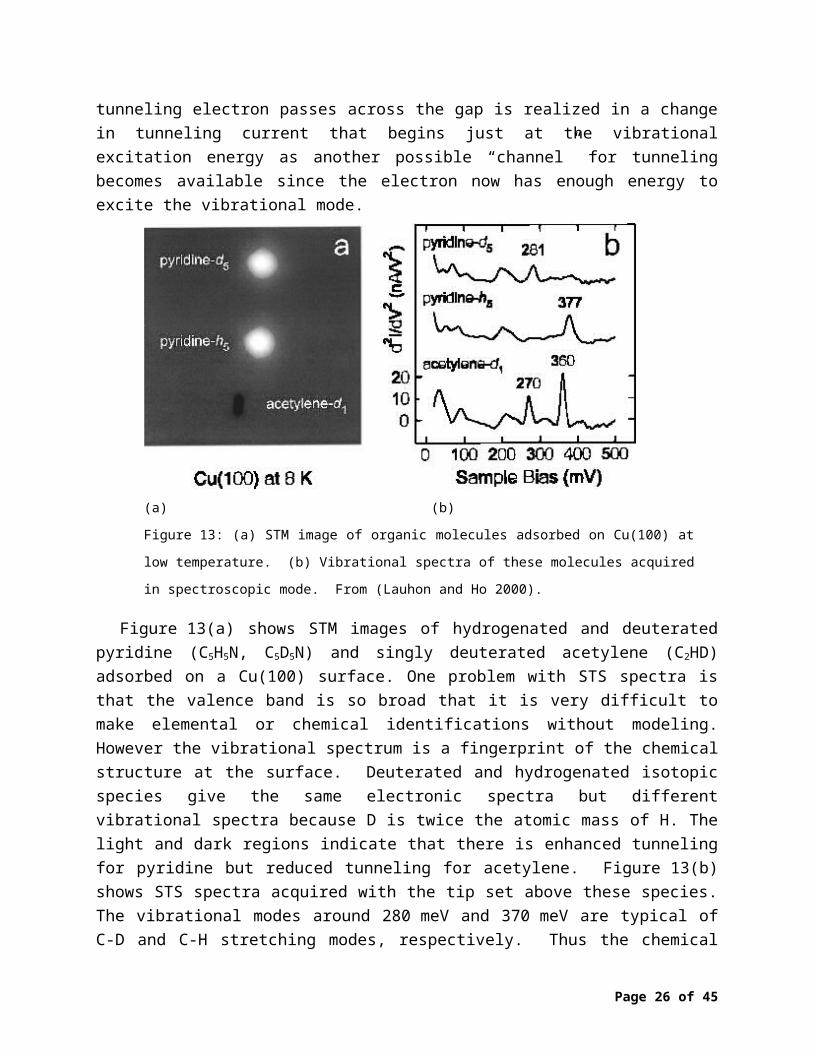
(a) (b)
Figure 13: (a) STM image of organic molecules adsorbed on Cu(100) at low temperature. (b)
Vibrational spectra of these molecules acquired in spectroscopic mode. From (Lauhon and Ho 2000).
Figure 13(a) shows STM images of hydrogenated and deuterated pyridine (C5H5N, C5D5N) and singly deuterated acetylene (C2HD) adsorbed on a Cu(100) surface. One problem with STS spectra is that the valence band is so broad that it is very difficult to make elemental or chemical identifications without modeling. However the vibrational spectrum is a fingerprint of the chemical structure at the surface. Deuterated and hydrogenated isotopic species give the same electronic spectra but different vibrational spectra because D is twice the atomic mass of H. The light and dark regions indicate that there is enhanced tunneling for pyridine but reduced tunneling for acetylene. Figure 13(b) shows STS spectra acquired with the tip set above these species. The vibrational modes around 280 meV and 370 meV are typical of C-D and C-H stretching modes, respectively. Thus the chemical integrity of individual molecules at the surface is probed. The positional dependence of the vibrational spectra gives a direct picture of the geometry of the molecule on the surface.
The spatial arrangement of fragmentation and reaction products can also be analyzed. Besides, spontaneous processes upon adsorption, it is found that the tunneling electrons (and higher energy electrons) from the tip can dissociate molecular adsorbates. The tip-induced
Page 20 of 35

fragmentation products can then be analyzed by vibrational spectra. For example, pyridine apparently dissociates to an -pyridyl (C5H4N) species (Lauhon and Ho 2000).
Chasing atoms – Dynamics of surface diffusionAtoms in crystals like to be in the most energetically favorable (i.e., the most stable)
positions. Crystal structures are periodic arrays of atoms that thermally vibrate about their most stable positions. Of course there can be “mistakes” – places where atoms are missing (vacancies) or extra atoms are inserted (interstitials). The local interactions caused by such localized perturbations can shift the positions of the surrounding atoms. Let us consider an isolated atom or molecule on a surface that likewise prefers to be at its lowest energy position. We might simply look at the corrugation formed by the surface atoms and guess that the preferred site for an adsorbed atom would be a position that maximizes its association with other surface atoms.
It takes a certain amount of energy to remove an atom from a surface (the bonding energy) and less energy for the atom to “jump” from corrugation to corrugation over the surface. This jumping, or diffusion, is a thermally activated process that obeys statistical laws. Diffusion is most likely to proceed along the easiest path along the surface such as along rows or channels of low-index single crystal surfaces. We say that there is an activation energy, Ea, for the atom to get over the barrier. The diffusion rate is given 1/ = o exp(-Ea/kT). is the mean residence time in a site (so 1/ is the mean diffusion rate), o is an attempt frequency for diffusion and should be of the order of the atomic vibration frequency in the potential well, and kT is the thermal energy (k is Boltzmann constant and T is the sample temperature in K). In general, other paths need not be considered because their higher activation energies greatly reduce their rates due to the exponential dependence.
In semiconductor technology, epitaxial growth has been developed; this is atom layer-by-layer growth performed under the right conditions by evaporating atoms on the clean surface, and allowing them to move over the surface and find each other until a new perfect atomic layer is formed.
STM can be used to measure the activation energy for diffusion as long as it can follow an atom. One way to do this is to take multiple images and make a movie to analyze. Unfortunately, in the >1 sec it takes to acquire an image of the surface that will contain the atom’s diffusion path, the atom may have moved. The atom might even be partially imaged once at one place and then at another just producing a blur in the final frame. Another novel approach to measure diffusion is to use an STM programmed as an “Atom Tracker.” The STM first takes a single frame at a relatively low temperature to find the atom of interest and then the tip is set
Page 21 of 35
above that atom; the STM control is then configured to only record the position of the one atom as it moves when the temperature is increased as a function of time.
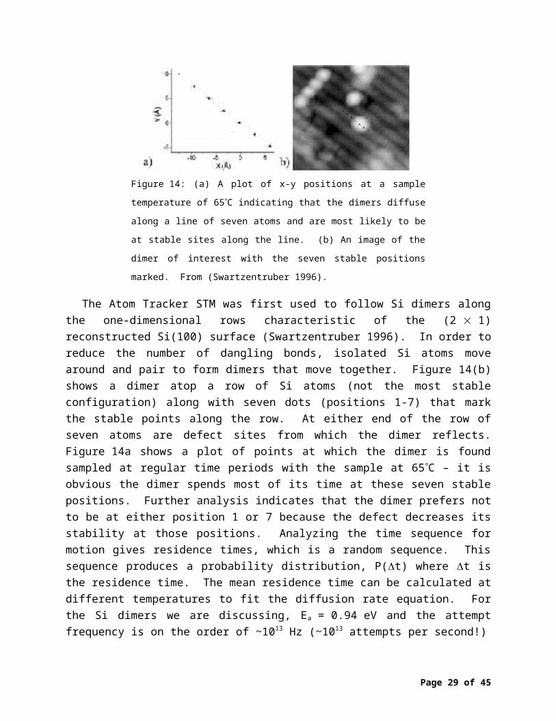
Figure 14: (a) A plot of x-y positions at a sample temperature of 65 C indicating
that the dimers diffuse along a line of seven atoms and are most likely to be at
stable sites along the line. (b) An image of the dimer of interest with the seven
stable positions marked. From (Swartzentruber 1996).
The Atom Tracker STM was first used to follow Si dimers along the one-dimensional rows characteristic of the (2 1) reconstructed Si(100) surface (Swartzentruber 1996). In order to reduce the number of dangling bonds, isolated Si atoms move around and pair to form dimers that move together. Figure 14(b) shows a dimer atop a row of Si atoms (not the most stable configuration) along with seven dots (positions 1-7) that mark the stable points along the row. At either end of the row of seven atoms are defect sites from which the dimer reflects. Figure 14a shows a plot of points at which the dimer is found sampled at regular time periods with the sample at 65C – it is obvious the dimer spends most of its time at these seven stable positions. Further analysis indicates that the dimer prefers not to be at either position 1 or 7 because the defect decreases its stability at those positions. Analyzing the time sequence for motion gives residence times, which is a random sequence. This sequence produces a probability distribution, P(t) where t is the residence time. The mean residence time can be calculated at different temperatures to fit the diffusion rate equation. For the Si dimers we are discussing, Ea = 0.94 eV and the attempt frequency is on the order of ~1013 Hz (~1013 attempts per second!)
The second method is to analyze STM “movies” provided that the speed at which the STM can take and store frames is balanced with the diffusion rate of a surface atom. A series of STM movie frames is shown for a platinum atom diffusing along a channel of the corrugated Pt(110) surface (Horch, Lorensen et al. 1999). In this case, atomic hydrogen adsorbed from the background gas (at ultrahigh vacuum) exhibits an apparent height increase for the Pt adatom due to a change in the local electronic structure. Most significantly, it was found that without H the activation barrier for diffusion is 0.81 eV but with H the diffusion barrier is lowered to 0.16 eV.
Page 22 of 35

Thus, H affects the local electronic structure and the diffusion barrier in such a way that Pt adatom diffusion is increased by a factor of ~500 at room temperature.
QuickTime™ and aGIF decompressor
are needed to see this picture.
Figure 15: A movie of H-assisted Pt atom diffusion along a Pt(110) row
at room temperature. The lines are Pt atomic rows of the crystal
surface, the circled protrusions represent a moving Pt atom with bright
features seen when atomic H is present as well. From (Horch,
Lorensen et al. 1999).
Measuring electrostatic forces and capacitance – Imaging the operation of microelectronics devices
Besides contact forces, an SPM can measure interaction forces that attract or repel the tip when it is out of contact or in contact. Van der Waals, magnetic, and electrostatic forces can be measured while the tip is an appropriate distance away from the surface. For a magnetic interaction, the tip must be coated with some magnetic material. For an electrostatic interaction upon which we will focus, the tip must be charged by applying a potential to a metal-coated tip. Measuring these non-contact forces typically requires that the tip be vibrated near its resonance frequency while it is scanning. Shifts from the resonance frequency indicate passage through a force gradient above the surface caused in this case by a varying electric field. From these variations, an image is constructed.
Microelectronics fabrication today is capable of making features ~200 nm in size. Often, the processes can create multilayer structures. Often a failure, such as a short, is caused by an imperfection in the circuit that would not be visible topographically because the composition of the elements are not visible to microscopy, particularly if they are beneath a resist or passivating layer. However, measuring the electrostatic behavior of an operating or biased device element essentially shows the distribution of charge. Figure 16 shows a topographic image (left) and an electric force image (right) of a packaged SRAM integrated circuit with voltages applied to specific bus lines. The topographic image clearly shows the structure with no apparent defects. However, the right image shows two three-pronged arrangments that comprise two transistors. The left transistor has charge between the second and third prong indicating a defect that is
Page 23 of 35
placing it in saturation. Thus measuring electric fields with SFM can be used to study device failure.
Figure 16: SFM (left) and electric force (right) image of SRAM
integrated circuit illustrating failure. From www.di.com.
An SPM can be operated with a high-frequency resonant capacitance sensor embedded in the tip to measure the spatial dependence of charge carriers in a semiconducting material. This has been demonstrated on a cross-section of a field effect transistor to visualize the conducting channel of a p-channel metal-oxide-semiconductor field effect transistor (Nakakura, Hetherington et al. 1999). Figure 17(a) is a sketch of such a device in which current between the source and drain is varied by changing the gate voltage and thus the concentration of charge carriers between them. Figure 17(b) shows capacitance images as a conduction path is being formed by varying the gate bias (the field-effect on the doped semiconductor). In these images, p-type regions appear bright. As the gate voltage goes from 0 V to –1.75 V, the carriers in the source begin to extend beneath the gate; when the gate voltage is at –3.0 V, the conduction path reaches to the drain and the semiconducting material is driven to a state of conduction as corroborated by simultaneously measuring the drain current.
Page 24 of 35
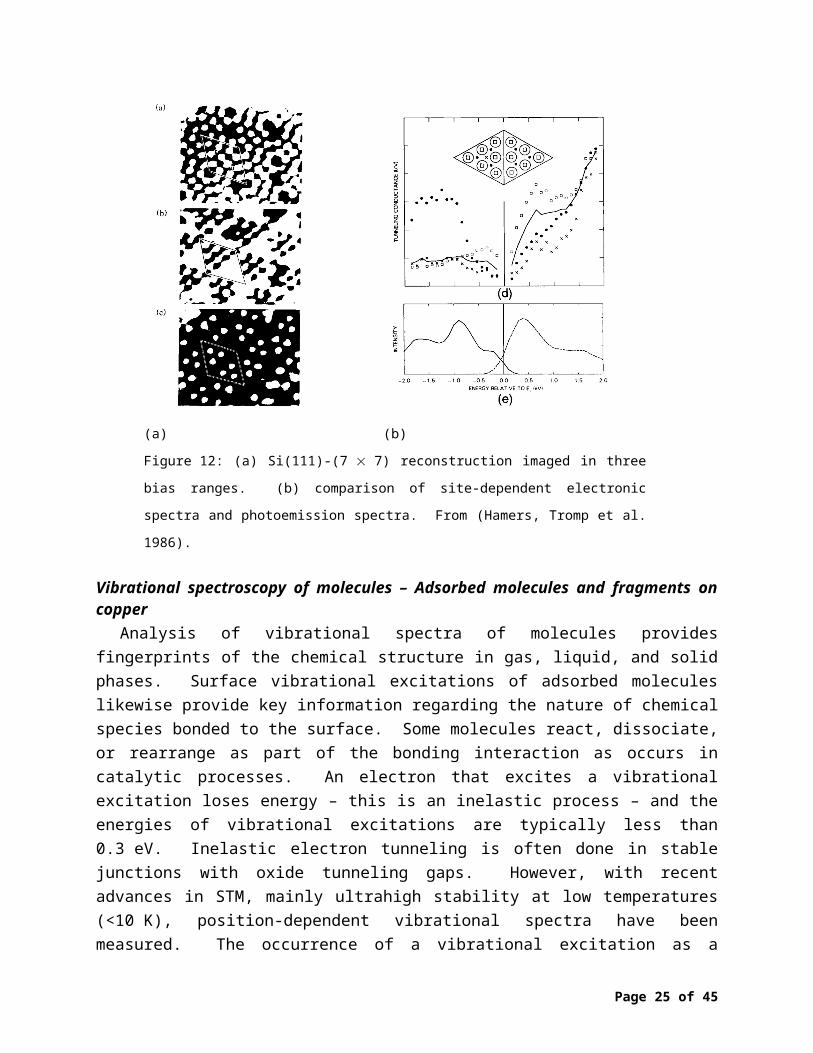
Figure 17: (a) Schematic of field effect transistor. (b) Cross-sectional scanning capacitance microscopy
images of field transistor in various modes o f operation. From (Nakakura, Hetherington et al. 1999).
Atomic manipulation – Writing with the STMWe have shown that force interactions between the tip and the surface can be characterized
by SFM. Force interactions between tip (STM, SFM) and the surface can be strong enough to displace or even remove atoms. These force interactions can come from van der Waals, chemical, or electrostatic forces and, if there is an electrical current between the tip and the sample, local electronic excitations can cause surface atoms to desorb. Think of a surface atom or an adsorbed atom sitting in its three-dimensional potential energy well – this traces the energy as a function of position for motion off the surface (normal) and for diffusion (along the surface). Typically, the energy barrier that must be overcome to remove the atom from a surface is larger than the barrier that confines the atom to a particular bonding site. Placing an SPM probe tip near an adsorbed atom allows the tip to controllably move the position of an atom on the surface and then to re-image the atom at its new position – essentially creating a read-write device. This capability was first demonstrated by researchers at IBM by moving xenon atoms on a Ni(100) at 4 K in ultrahigh vacuum to write “IBM” as shown in Figure 18 (Eigler and Schweizer 1990). The lettering is similar to the images formed by a dot-matrix printer. Xe is a noble gas and the van der Waals interaction of Xe with the metal surface is weak, so that low temperatures are necessary to keep the atom on the surface. The operation proceeds as follows: the Ni surface is exposed to much less than a monolayer of Xe (the atoms stick at random locations); the STM tip is scanned to find a Xe atom, the tip is placed over a Xe atom and lowered to increase the
Page 25 of 35
interaction force; the tip is moved laterally to drag the atom to the desired location (write); the tip is moved vertically to break free of the Xe atom; the tip is scanned over the surface to read the new position. Writing with atoms obviously creates a non-equilibrium configuration. This accomplishment was not so practical considering in terms of information storage because of the low temperature requirement, but it demonstrated the potential to obtain the highest physical information density possible. Since then manipulation of more tightly bound atoms or groups of atoms at higher temperatures has been demonstrated.
Figure 18: Atomic manipulation of xenon atoms
on a nickel surface. From (Eigler and Schweizer
1990)
Returning to adsorbed Xe atoms, it was shown that applying electrical voltage pulses of opposite polarities to the tip could controllably transfer a Xe atom from the surface to the tip and back again. This capability was referred to as an atomic switch (Eigler, Lutz et al. 1991) because not only was the position of the atoms changed, but also the tunneling conductance changed resulting in a two-state system. The conductance depends on the local environment of the Xe atom because there are different electronic states available for tunneling. The possibility to identify, manipulate or switch (write) and image (read) individual atoms represents one of the highest density storage mechanisms one could imagine.
Electronic structure manipulation – Electron wavefunctions in quantum corralsAdsorbed atoms or steps on a surface modify the local electronic structure enough such that
mobile electrons on the surface feel a potential barrier to motion. In the wave picture for electrons, at a potential barrier, there are finite probabilities for transmission and reflection. For a bounded wavelike system, standing waves are set up because of the requirements at the boundaries, and these are related to specific energy states, similar to distinct, or quantized, energy levels for electrons in atomic orbitals. Using the STM to create a very small closed boundary with Fe atoms on Cu, researchers at IBM have created “quantum corrals” (Crommie, Lutz et al. 1993). Because each electron standing wave corresponds to a unique energy, confining electrons in this way represents engineering a new energy spectrum that depends on the electron transport characteristics and the size of the corral.
Page 26 of 35

(a) (b)
Figure 19: (a) Construction of quantum corral. (b) An stadium structure showing electron
standing waves. From www.almaden.ibm.com/vis/stm.
Figure 19(a) shows the assembly of a 7.1 nm diameter circular corral made of 48 iron atoms (also see Figure 1). The ability to create new structures and new energy levels suggests a new approach to engineering electronic devices. The ripples in the images are spectroscopic pictures of the discrete states of the confined electrons and directly demonstrate the existence of quantum mechanical electron standing waves, which can also be modeled. Other confined configurations, such as the stadium shown in Figure 19(b) show that the standing wave patterns largely adopt the shape of the boundary.
Building components and devices for nanoelectronicsWhen electron conduction takes place through a very narrow region, theory predicts that the
values of conductance are quantized and that the values occur in discrete steps with a minimum value (essentially a current per wire channel) of , where e is the electronic charge and h is Planck's constant (Scheer, Agraït et al. 1998). Thus, as a wire gets thinner and thinner, say to the width of a single atom, the conductance should reach this minimum value before the wire breaks. This is another example where quantum effects become important as device dimensions shrink to the nanometer scale such that non-classical rules for electron transport apply. There have been several reports of quantized conductance such as at the point where an STM tip just touches a surface (Pascual, Méndez et al. 1993). Since atoms interact as they come closer, the same interatomic forces that apply in a solid cause atomic rearrangements, or distortions, at the apex so that atoms at the thin connection might adopt different interatomic distances than in the bulk.
Page 27 of 35

Figure 20: (a) Quantized conductance of an ultrathin wire. (b)
TEM image and (d) model of the wire. From (Ohnishi, Kondo et
al. 1998).
A unique STM combined with a Transmission Electron Microscope was used to directly view the structure of Au-Au tip-surface contacts (Ohnishi, Kondo et al. 1998). Figure 20 shows TEM images of two-atomic-row and one-atomic-row connections; a ball model is also shown. These were created after the tip was initially touched by a gold surface creating a contact of several atoms and then retracted to pull the connection into atomic strings. The conductance is quantized (2 Go and 1 Go, respectively) for these connections, before the wire is broken. It has been noted that these "wires" are quite robust – currents of 80 A at 1 V (current density of 1014 A/m2!) have been shown to flow through similar structures for greater than an hour. Further analysis has shown that average Au interatomic spacing is in the 0.35-0.40 nm range. Calculations predict not only that cleavage would occur at interatomic distances of ~0.31 nm but also that spontaneous pairing of atoms in a one-dimensional row (called a Peierls distortion) would be expected and this results in a non-conducting atomic chain (Okamoto and Takayanagi 1999).
Page 28 of 35
(a) (b)
Figure 21. (a) STM image of single-wall carbon nanotube. From (Odom, Huang et al. 1998). (b) SFM image of
overlapping carbon nanotubes. From (Avouris, Hertel et al. 1999)
Carbon nanotubes represent another type of ultrathin conductor (or semiconductor) that can be manipulated on surfaces by mechanical means between electrodes and then operated as nanoscale devices. Carbon nanotubes are composed of graphite sheets that are rolled into cylinders – they can be grown in single-walled or multi-walled configurations. Depending on how the sheets close on themselves (the helicity of the wrapping), nanotubes exhibit conducting or semiconducting electrical properties. Many proposed applications from mechanical reinforcements, to chemical/drug delivery devices, to electron emitters, to ultrasharp, chemically-treated SFM probes have been proposed and prototyped in this exploding area of research and development.
Page 29 of 35

Figure 22 Figure 23
Figure 22: Construction of a nanotube circuit. From (Avouris, Hertel et al. 1999).
Figure 23. Schematic nanotube field effect transistor and its electrical characteristics. From (Martel, Schmidt et al.
1998).
The STM image of a carbon nanotube shown in Figure 21(a) exhibits the hexagonal structure of carbon atoms seen on graphite (Odom, Huang et al. 1998). Nanotubes can be moved in a controlled fashion by an SFM tips but they adhere to surfaces quite strongly. In the configuration of Figure 21(b) in which one nanotube crosses another is studied in detail, it is found that a balance of the adhesion force and the strain of deformation will determine the curvature of the overlaying nanotube (Avouris, Hertel et al. 1999). Thus the mechanical properties at these small scales are very interesting. In terms of electronics applications, Figure 22 shows a sequence in which a ~2 m conducting carbon nanotube is moved between two gold contacts and then its resistance is measured (Avouris, Hertel et al. 1999). The straight-line I-V characteristic shows that it is ohmic, but many cases show non-ohmic behavior. This is attributed not to the nanotube properties but to the poor quality of the contact, which can be remedied by electron irradiation. Figure 23 shows a sketch of a single-walled carbon nanotube on top of an (insulating) oxide layer on a silicon substrate (Martel, Schmidt et al. 1998). The nanotube has been manipulated between two electrodes to become the active element of a nanotube field effect transistor (FET). Current passed between the source and the drain is controlled by the voltage applied to the Si because the resulting electric field changes the carrier properties of the nanotube. Familiar FET transfer characteristic curves (current vs. gate voltage
Page 30 of 35

for several source-to-drain voltages) are shown. Further analysis has demonstrated that conduction in this device is by positive holes, a familiar charge carrier in semiconductor physics. Even more complex nanotube circuits can be constructed by STM using the tip to deform, cut, lift, and translate the “components” on the substrate surface.
Measuring interatomic and intermolecular bonding forces in biochemistryOne of the practical problems of imaging macromolecules using SFM is that they may not be
rigidly attached to the surface, perhaps only attached at a few points. Thus, the tip might stick to a part of the molecule and the molecule will move during a scan giving at best a blurred image. When the tip is retracted, there might be an increased non-specific force to break loose of the surface material. The exact positions at which the tip and surface are attached to a long-chain molecule are not so controllable. However in light of the extreme force sensitivity of SFM, pulling a molecule attached to both the tip and substrate until it breaks offers the potential for the measurement of single bond forces and molecular manipulation. For intertwined long chain molecules, such as proteins, the force vs. molecular extension relates to the bonding forces (remember the tip deflection is directly related to force) along the chain as well as intermolecular forces between chain segments, such as protein-folding forces.
Figure 24: (a) Illustration of pulling a macromolecule anchored on tip and sample surface. (b) Force curve for
amylose polysaccharide. From (Grandbois, Beyer et al. 1999).
Page 31 of 35

One such study has measured the covalent attachment force of amylose, a polysaccharide depicted in Figure 24 as a chain of aromatic rings, to the glass (SiO2) surface and an SiO2 SFM tip (Grandbois, Beyer et al. 1999). A coupling agent with amino functional groups was applied to both the substrate and tip, amylose was deposited on the surface and covalently attached (presumably at multiple sites as shown), and the tip was gently lowered into the material. Monitoring the tip deflection (pulling force) as the substrate was initially pulled away indicated that some bonds related to intermolecular rearrangements were being broken. Beyond this regime it is found that a single stretched amylose molecule maintains a constant force of ~275 pN as it is stretched as the rings elongate. Thus, a plateau at this force during extension indicates that a single molecule is being stretched between tip and substrate. Once the molecule is stretched further, the force increases and multiple irreversible steps appear in the force curve as covalent attachment rupture until all are broken and the force goes to zero. Analysis of the rupture forces of several bonds gives an average rupture force of ~2 nN. In order to determine to what specific covalent attachment this corresponds, calculations of interatomic bonding forces were carried out with the most likely candidate being a Si-C bond.
(a) (b)
Figure 25: (a) Illustration of pulling a protein anchored on tip and sample surface. (b) Force curve for
native spectrin. From (Rief, Pascual et al. 1999).
Figure 25(a) presents a sketch of the mechanical unfolding of a protein consisting of a string of repeat units in an experiment that probes intermolecular folding forces (Rief, Pascual et al.
Page 32 of 35

1999). Figure 25(b) shows a force curve for the protein spectrin that exhibits repeats every ~32 nm apart. Each native spectrin unit contains two types of chains ( and ) and consists of ~106 amino acid residues in a coiled structure that is about 32 nm in length. Thus, the observed separation between peaks in the force curve represents the length of the repeat units. The heights of the peaks represent the force required to overcome the interaction two repeat units and thus unfold the protein. The data is fit with a model that includes contributions of the elasticity of the repeat units. Thus the unfolding force is on the order of 25-35 pN, about 10 times weaker than the force of a covalent attachment as discussed previously. It is important to note that if the tip is brought back towards the surface, the protein folds and curve traces will repeat when the protein is pulled again, that is, the process is reversible. SFM instrumentation has been demonstrated to probe forces <10-15 N.
PROSPECTS
We have shown that scanning probe microscopes are providing a new way to create and explore the exciting world of nanotechnology. New scientific advances and technique development are bringing our everyday view to an increasingly smaller level where unfamiliar principles often apply. The topics we have discussed range from fundamental physics and chemistry to electronics devices, coatings, and biotechnology. As nanoscale science advances and techniques of nanotechnology are refined, the ability to characterize and manipulate atoms, molecules, and biological macromolecules at surfaces opens the door to a new age of engineering - controlling and probing the structure and physical properties of materials atom-by-atom. Nanotechnology defines a new area that will excite the creativity of scientists and engineers to make discoveries about nature and to apply these discoveries for many years.
REFERENCESAvouris, P., T. Hertel, et al. (1999). “Carbon nanotubes: nanomechanics, manipulation, and electronic devices.”
Appl. Surf. Sci. 141: 201-209.
Binnig, G., C. F. Quate, et al. (1986). “Atomic Force Microscope.” Phys. Rev. Lett. 56: 930-933.
Binnig, G., H. Rohrer, et al. (1982). “Tunneling through a controllable vacuum gap.” Appl. Phys. Lett. 40(2): 178-
180.
Crommie, M. F., C. P. Lutz, et al. (1993). “Confinement of electrons to quantum corrals on a metal surface.”
Science 262: 218-220.
Page 33 of 35

DiNardo, N. J. (1994). Nanoscale Characterization of Surfaces and Interfaces. Weinheim, VCH.
Drexler, K. P. (1990). Engines of Creation: The Coming Era of Nanotechnology, Fourth Estate.
Eigler, D. M., C. P. Lutz, et al. (1991). “An atomic switch realized with the scanning tunnelling microscope.” Nature
352: 600-603.
Eigler, D. M. and E. K. Schweizer (1990). “Positioning single atoms with a scanning tunnelling microscope.” Nature
344: 524-526.
Feynman, R. P. (1959). Plenty of Room at the Bottom.
Grandbois, M., M. Beyer, et al. (1999). “How strong is a covalent bond?” Science 283(4): 1727-1730.
Hamers, R. J., R. M. Tromp, et al. (1986). “Surface electronic structure of Si(111)-7x7 resolved in real space.” Phys.
Rev. Lett. 56: 1972-1975.
Horch, S., H. T. Lorensen, et al. (1999). “Enhancement of surface self-diffusion of platinum atoms by adsorbed
hydrogen.” Nature 398(11 March 1999): 134-136.
Lauhon, L. J. and W. Ho (2000). “Single-molecule chemistry and vibrational spectroscopy: Pyridine and benzene on
Cu(001).” J. Phys. Chem. A 104(11): 2463-2467.
Martel, R., T. Schmidt, et al. (1998). “Single- and multi-wall carbon nanotube field-effect transistors.” Appl. Phys.
Lett. 73(17): 2447-2449.
Nakakura, C. Y., D. L. Hetherington, et al. (1999). “Observation of metal-oxide-semiconductor transistor operation
using scanning capacitance microscopy.” Appl. Phys. Lett. 75(15): 2319-2321.
Odom, T. W., J.-L. Huang, et al. (1998). “Atomic structure and electronic properties of single-walled carbon
nanotubes.” Nature 391(1 January 1998): 62-64.
Ohnishi, H., Y. Kondo, et al. (1998). “Quantized conductance through individual rows of suspended gold atoms.”
Nature 395(22 October 1998): 780-783.
Okamoto, M. and K. Takayanagi (1999). “Structure and conductance of a gold atomic chain.” Phys. Rev. B 60(11):
7808-7811.
Pascual, J. I., J. Méndez, et al. (1993). “Quantum contact in gold nanostructures by scanning tunneling microscopy.”
Phys. Rev. Lett. 71(12): 1852-1855.
Rief, M., J. Pascual, et al. (1999). “Single molecule force spectroscopy of spectrin repeats: Low unfolding forces in
helix bundles.” J. Mol. Biol. 286: 553-561.
Scheer, E., N. Agraït, et al. (1998). “The signature of chemical valence in the electrical conduction through a single-
atom contact.” Nature 394(9 July 1998): 154-157.
Swartzentruber, B. S. (1996). “Direct measurement of surface diffusion using atom-tracking scanning tunneling
microscopy.” Phys. Rev. Lett. 76(3): 459-462.
Young, R., J. Ward, et al. (1972). “The topografiner: An instrument for measuring surface microtopography.” Rev.
Sci. Instrum. 43: 999-1011.
Page 34 of 35

Page 35 of 35