Embed Size (px)
Citation preview

Fabrication and Characterization of Semiconductor Ion Traps for
Quantum Information Processing
by
Daniel Lynn Stick
A dissertation submitted in partial fulfillmentof the requirements for the degree of
Doctor of Philosophy(Physics)
in The University of Michigan2007
Doctoral Commitee:
Professor Christopher R. Monroe, ChairProfessor Georg RaithelProfessor Jens ZornAssociate Professor Cagliyan KurdakAssistant Professor Yaoyun Shi

©Daniel Lynn Stick
All Rights Reserved2007

“I aint no bum, Mick. I aint no bum.”
– Rocky Balboa

To my parents
ii
ACKNOWLEDGEMENTS
First, I would like to thank Chris Monroe for his guidance in my scientific career.
I was unsure of what sub-field of physics that I wanted to pursue before I applied to
graduate school, and it was the tour that he gave when I visited Michigan that sold
me on this research. The responsibility he gave me early in my graduate career gave
me confidence in my abilities, and his “forget your classes” attitude freed up a lot of
time for research. I feel very fortunate to have had him as an advisor.
Winfried Hensinger has also had a profound impact on me; his determination and
painful-yet-ultimately-successful commitment to searching parameter space ingrained
in me the importance of hard work. I spent many long days and long nights in the lab
with Winni, and greatly appreciate his friendship and influence on me as a scientist.
During my first few years of research I spent a good fraction of my time at the
Laboratory for Physical Sciences (LPS), where I used the cleanroom to fabricate ion
traps in collaboration with Keith Schwab. His frequent fabrication advice and will-
ingness to help were instrumental in the ultimate success of this project. I will have
fond memories of my time spent at LPS not just from the draining but strangely
satisfying cleanroom work, but also from the camaraderie with Keith and the other
researchers there. In particular Kevin Eng was an invaluable source of practical fab-
rication knowledge, and is responsible for helping me develop several key processing
steps. I also want to acknowledge additional help from Benedetta Camarota, Carlos
Sanchez, Kenton Brown, Dan Sullivan, Akshay Naik, Matt LaHaye, Olivier Buu, Har-
ish Bhaskaran, and Alex Hutchinson. The staff at LPS was also extremely helpful, in
particular Scott Horst and Steve Brown for their ICP help, Lisa Lucas for equipment
iii

training, Toby Olver for general advice and trouble shooting, Lynn Calhoun for MBE
growth, Russell for wafer thinning, and Les Lorenz for machining. Without all these
people supporting me with their expertise and direct help I am sure that my best
efforts would have been in vain.
I could not have asked for a better lab to work in at Michigan. My lab mates have
made my time here very enjoyable and have been instrumental in my training as a
scientist. I need to particularly acknowledge those who I have worked closely with on
the GaAs microtrap projects with, including Martin Madsen for developing the idea
of a semiconductor fabricated trap, and Winfried Hensinger and Steve Olmschenk for
testing it. During the T trap project I had the privilege of also working with Dave
Hucul and Mark Yeo in both the construction and testing phases. Few graduate
school memories remain as vivid to me as listening to the Tijuana Brass late at
night while working on the T trap vacuum chamber. Again, Winni’s persistence in
the construction of this trap helped push us through whatever design flaws we had
chosen to implement.
Recently I have had the pleasure of working closely with Jon Sterk, Liz Otto, Dan
Cook, and Yisa Rumala. I have spent a lot of time with Jon in particular over the
last few years, and owe him for the hard work that he spent on the vacuum chamber
design and novel trap testing. I know the project is in capable hands as he assumes
leadership of this project. Working with these other new students as they entered
the lab has helped me immensely; their questions have made me think through ideas
that I had grown to assume, and their new perspectives have injected a needed dose
of creativity into the experiment.
Although I haven’t worked as closely with the other lab members as I have with
those on my experiment, they have all been very helpful in broadening my knowledge
of atomic physics. In particular, I have had many interesting and useful physics
discussions with Louis Deslauriers, as well as interesting discussions outside of physics.
Through interactions in group meetings, doing general lab work, around the coffee
maker, I am grateful for their friendship and scientific skills. Paul Haljan, Boris
Blinov, Ming-Shien Chang, Dzmitry Matsukevich, Peter Maunz, Dave Moehring,
iv

Kelly Younge, Andrew Chew, Rudy Kohn, Russ Miller, Mark Acton, Kathy-Anne
Brickman, and Patty Lee have all made my experience in Chris’ lab a wonderful one.
Over the last few years I have been fortunate to interact with other groups and
researchers. In particular Dave Wineland, John Bollinger, and their students at NIST
have always been willing to give advice, and the combined advances we have made, as
well as those in the other ion trapping groups at Oxford and Innsbruck, have proved
the efficacy of collaboration over competition. I am also very grateful to Dick Slusher
and Matt Blain for their foundry work on ion traps which we have tested. Without
their efforts this field would not be attracting the attention today, and I sincerely
wish them well in the future. Michael Pedersen, who I have never met but who is
working at MEMS Exchange on building us an ion trap, also deserves recognition in
the trap development category. I would be remiss if I did not express a great deal of
thanks to Henry Everitt, who is responsible in no small part for the generous support
of novel ion trap development for quantum computing. I also want to thank Jun Ye
and Ben Lev for their help with my NRC application.
Those who laid the framework for my physics career deserve thanks as well. Mrs.
Knighton, my middle school science teacher, and particularly Mr. Wood, my high
school physics teacher, did more than they can imagine in fostering and supporting
my love of science. They have been influential in both my scientific career and the
many others they have taught. As an undergraduate at Caltech, I was blessed to
do research with both Hideo Mabuchi and Erik Winfree. I’m sure they put up with
plenty of frustrating moments as I was just getting my feet wet in research, but I am
extremely happy that they stuck with me.
Also I need to thank the other members of my committee, comprising Yaoyun Shi,
Cagliyan Kurdak, Jens Zorn, and Georg Raithel. I have been fortunate to interact
with all of these faculty members in my prelim and outside of it. The field of quantum
computing is a large and growing one, in no small part to the theoretical work being
done by those like Prof. Shi. Prof. Kurdak has been generous with offering fabrication
advice as well as facilities for annealing our recepticles. As my E&M teacher, Prof.
Raithel was a thorough instructure, as well as a flexible one when I needed to do
v

fabrication work in Washington. I saw Prof. Zorn fairly regularly in the hallway and
the machine shop, and enjoyed our conversations and the advice he gave.
This is the catch-all paragraph for things I want to say which do not fit anywhere
else. For one, I hold Keith and Winni most responsible for my original coffee addiction,
and Chris for helping secure it with his purchase of the Gaggia Titanium. If I had to
pick the inanimate object I will miss the most, it is this fantastic marvel of engineering.
I also need to thank Rich Vallery for his help with the latex class file which I used
for formatting this thesis.
I also need to thank all my friends who have made my graduate school experience
a wonderful one. I won’t thank the guys I play poker with every week, as I feel like my
rough streak over the last few months and the money I have given you are enough. Li
Yu, Misty Richards, Annamarie Pluhars, and Bob Sherwood in Washington - thank
you for your hospitality. To my friends at GCF and Campus Chapel, particularly Rolf
Bouma and Mark Roeda, thank you for your spiritual guidance and support. The
creation that I have the privilege to investigate makes my life exciting and rewarding.
Finally, to my family, I owe perhaps the most. My dad and mom who pushed me
to do well in school and fostered a recreational interest in science and math through
outside engineering and science projects - you have been wonderful parents. I suppose
after 27 years of informal education combined with 21 years of formal education, I
might be ready to get a real job. And to you, Christina, for being so supportive of
my work and putting up with my blank stares as I zone out into the work of atomic
physics, I want to thank you with all my heart. Hopefully my lifelong love will be a
sufficient thank you. If not, there’s the prestige of being married to a PhD physicist.
vi

TABLE OF CONTENTS
DEDICATION . . . . . . . . . . . . . . . . . . . . . . . . . . . . . . . . . . ii
ACKNOWLEDGEMENTS . . . . . . . . . . . . . . . . . . . . . . . . . . iii
LIST OF TABLES . . . . . . . . . . . . . . . . . . . . . . . . . . . . . . . . x
LIST OF FIGURES . . . . . . . . . . . . . . . . . . . . . . . . . . . . . . . xi
ABSTRACT . . . . . . . . . . . . . . . . . . . . . . . . . . . . . . . . . . . xiv
CHAPTER
1. Introduction to trapped ion quantum computing . . . . . . . . . 1
1.1 Trapped Ions . . . . . . . . . . . . . . . . . . . . . . . . . . . . . 11.2 Moore’s law and classical computing . . . . . . . . . . . . . . . . 21.3 Quantum Information . . . . . . . . . . . . . . . . . . . . . . . . 31.4 General quantum computing requirements . . . . . . . . . . . . . 51.5 Quantum phenomena . . . . . . . . . . . . . . . . . . . . . . . . . 51.6 What numbers are we really talking about? . . . . . . . . . . . . 71.7 Atomic physics of trapped ion quantum computing . . . . . . . . 8
2. The cadmium qubit . . . . . . . . . . . . . . . . . . . . . . . . . . . 10
2.1 State detection and initialization . . . . . . . . . . . . . . . . . . 102.2 Qubit rotations and quantum gates . . . . . . . . . . . . . . . . . 11
2.2.1 The ion’s motion . . . . . . . . . . . . . . . . . . . . . . . 122.2.2 The ion’s internal states . . . . . . . . . . . . . . . . . . . 132.2.3 Microwave transitions . . . . . . . . . . . . . . . . . . . . . 162.2.4 Stimulated Raman Transitions . . . . . . . . . . . . . . . . 172.2.5 Laser cooling . . . . . . . . . . . . . . . . . . . . . . . . . 222.2.6 Thermometry . . . . . . . . . . . . . . . . . . . . . . . . . 23
3. Ion trapping fundamentals . . . . . . . . . . . . . . . . . . . . . . . 26
3.1 The ponderomotive potential . . . . . . . . . . . . . . . . . . . . . 263.2 The Mathieu equation . . . . . . . . . . . . . . . . . . . . . . . . 263.3 The pseudo-potential approximation . . . . . . . . . . . . . . . . 313.4 The 3 dimensional hyperbolic electrode trap . . . . . . . . . . . . 32
vii

3.4.1 Ring and Fork Trap . . . . . . . . . . . . . . . . . . . . . . 333.4.2 Needle trap . . . . . . . . . . . . . . . . . . . . . . . . . . 36
3.5 Linear traps . . . . . . . . . . . . . . . . . . . . . . . . . . . . . . 363.5.1 Four rod trap . . . . . . . . . . . . . . . . . . . . . . . . . 383.5.2 Single layer trap . . . . . . . . . . . . . . . . . . . . . . . . 503.5.3 Three layer trap . . . . . . . . . . . . . . . . . . . . . . . . 52
3.6 The surface trap . . . . . . . . . . . . . . . . . . . . . . . . . . . 523.7 Computer simulations of electric fields from electrodes . . . . . . 53
4. Experimental setup . . . . . . . . . . . . . . . . . . . . . . . . . . . 59
4.1 Achieving ultra high vacuum (UHV) . . . . . . . . . . . . . . . . 594.2 The bake . . . . . . . . . . . . . . . . . . . . . . . . . . . . . . . . 594.3 The chamber . . . . . . . . . . . . . . . . . . . . . . . . . . . . . 614.4 RF resonator . . . . . . . . . . . . . . . . . . . . . . . . . . . . . 634.5 Ovens . . . . . . . . . . . . . . . . . . . . . . . . . . . . . . . . . 664.6 Photoionization . . . . . . . . . . . . . . . . . . . . . . . . . . . . 684.7 Lasers and frequency modulation . . . . . . . . . . . . . . . . . . 704.8 Imaging system . . . . . . . . . . . . . . . . . . . . . . . . . . . . 744.9 Instrument control and data collection . . . . . . . . . . . . . . . 75
5. Scalability: Demonstrating junctions in the T trap . . . . . . . 79
5.1 T trap fabrication . . . . . . . . . . . . . . . . . . . . . . . . . . . 815.1.1 Photolithography . . . . . . . . . . . . . . . . . . . . . . . 825.1.2 Dry film photoresist . . . . . . . . . . . . . . . . . . . . . . 83
5.2 Trap layout and electronics . . . . . . . . . . . . . . . . . . . . . . 845.3 Shuttling results . . . . . . . . . . . . . . . . . . . . . . . . . . . . 855.4 T trap lessons . . . . . . . . . . . . . . . . . . . . . . . . . . . . . 86
6. Scalability: Demonstrating a microfabricated gallium arsenidetrap . . . . . . . . . . . . . . . . . . . . . . . . . . . . . . . . . . . . . 92
6.1 Mechanical characterization . . . . . . . . . . . . . . . . . . . . . 926.2 Power dissipation . . . . . . . . . . . . . . . . . . . . . . . . . . . 946.3 Power scaling laws . . . . . . . . . . . . . . . . . . . . . . . . . . 966.4 Gallium Arsenide properties and MBE Growth . . . . . . . . . . . 986.5 GaAs trap fabrication . . . . . . . . . . . . . . . . . . . . . . . . 100
6.5.1 Scribing, dicing, and thinning . . . . . . . . . . . . . . . . 1006.5.2 Photoresist and standard procedures . . . . . . . . . . . . 1026.5.3 Backside etching . . . . . . . . . . . . . . . . . . . . . . . . 1036.5.4 Bondpad etching . . . . . . . . . . . . . . . . . . . . . . . 1086.5.5 Ohmic Contacts . . . . . . . . . . . . . . . . . . . . . . . . 1116.5.6 Cantilever etching . . . . . . . . . . . . . . . . . . . . . . . 1136.5.7 Annealing . . . . . . . . . . . . . . . . . . . . . . . . . . . 1136.5.8 Al.7Ga.3As etch . . . . . . . . . . . . . . . . . . . . . . . . 113
viii

6.5.9 Attaching to chip carrier . . . . . . . . . . . . . . . . . . . 1146.5.10 Interconnects, RF grounding, and filtering . . . . . . . . . 115
6.6 Experimental results . . . . . . . . . . . . . . . . . . . . . . . . . 1186.6.1 Operating parameters . . . . . . . . . . . . . . . . . . . . . 1186.6.2 Motional heating . . . . . . . . . . . . . . . . . . . . . . . 1216.6.3 Motionally sensitive carrier transition . . . . . . . . . . . . 124
6.7 Future work on two layer traps . . . . . . . . . . . . . . . . . . . 130
7. Other microfabricated traps . . . . . . . . . . . . . . . . . . . . . . 133
7.1 Lucent trap . . . . . . . . . . . . . . . . . . . . . . . . . . . . . . 1337.1.1 Fabrication . . . . . . . . . . . . . . . . . . . . . . . . . . 1337.1.2 Simulations . . . . . . . . . . . . . . . . . . . . . . . . . . 1347.1.3 Operating parameters and results . . . . . . . . . . . . . . 139
7.2 Sandia trap . . . . . . . . . . . . . . . . . . . . . . . . . . . . . . 1437.3 Polysilicon MEMS Exchange trap . . . . . . . . . . . . . . . . . . 146
8. Sources of motional heating . . . . . . . . . . . . . . . . . . . . . . 150
8.1 Heating rate and spectral density of electric field noise . . . . . . 1518.2 Thermal (Johnson) noise . . . . . . . . . . . . . . . . . . . . . . . 1528.3 Trap construction . . . . . . . . . . . . . . . . . . . . . . . . . . . 1538.4 Heating results . . . . . . . . . . . . . . . . . . . . . . . . . . . . 1548.5 Future work - molybdenum trap . . . . . . . . . . . . . . . . . . . 156
9. Conclusion . . . . . . . . . . . . . . . . . . . . . . . . . . . . . . . . . 158
BIBLIOGRAPHY . . . . . . . . . . . . . . . . . . . . . . . . . . . . . . . . 159
ix

LIST OF TABLES
Table1.1 A CNOT gate truth table . . . . . . . . . . . . . . . . . . . . . . . . 96.1 ICP settings . . . . . . . . . . . . . . . . . . . . . . . . . . . . . . . . 1116.2 CHA Recipe . . . . . . . . . . . . . . . . . . . . . . . . . . . . . . . . 1126.3 Annealing recipe . . . . . . . . . . . . . . . . . . . . . . . . . . . . . 114
x

LIST OF FIGURES
Figure2.1 Detection and initialization of the 111Cd+ qubit . . . . . . . . . . . . 122.2 Detection statistics for the 111Cd+ qubit in the dark and bright states 132.3 Rabi flopping on the carrier transition using microwaves . . . . . . . 182.4 Raman transition diagram . . . . . . . . . . . . . . . . . . . . . . . . 192.5 Schematic of the laser beams used in the detection, initialization, and
motional coupling of an ion . . . . . . . . . . . . . . . . . . . . . . . 202.6 Energy level diagram of Raman transitions and Clebsch-Gordan coef-
ficients . . . . . . . . . . . . . . . . . . . . . . . . . . . . . . . . . . . 212.7 Raman spectra showing the sideband asymmetry . . . . . . . . . . . 253.1 Ideal hyperbolic trap . . . . . . . . . . . . . . . . . . . . . . . . . . . 323.2 Stability diagram for an ideal hyperbolic trap . . . . . . . . . . . . . 343.3 Ring and fork trap . . . . . . . . . . . . . . . . . . . . . . . . . . . . 353.4 Two needle trap . . . . . . . . . . . . . . . . . . . . . . . . . . . . . . 363.5 Linear traps . . . . . . . . . . . . . . . . . . . . . . . . . . . . . . . . 373.6 Ideal linear hyperbolic trap . . . . . . . . . . . . . . . . . . . . . . . 383.7 Stability diagram for hyperbolic linear trap . . . . . . . . . . . . . . . 393.8 Two layer linear trap . . . . . . . . . . . . . . . . . . . . . . . . . . . 413.9 Trap strength and depth as a function of the aspect ratio . . . . . . . 423.10 Conformal mapping of a two layer trap to parallel plate capacitors . . 443.11 Higher order anharmonic coefficients of the two layer trap at the trap
center . . . . . . . . . . . . . . . . . . . . . . . . . . . . . . . . . . . 463.12 Higher order anharmonic coefficients of the two layer trap as a function
of distance from the trap center . . . . . . . . . . . . . . . . . . . . . 473.13 Contour plot of the ponderomotive potential for a trap with rotated
principal axes . . . . . . . . . . . . . . . . . . . . . . . . . . . . . . . 493.14 Bridge junction for a two layer trap . . . . . . . . . . . . . . . . . . . 513.15 Single layer trap geometry . . . . . . . . . . . . . . . . . . . . . . . . 523.16 Three layer trap . . . . . . . . . . . . . . . . . . . . . . . . . . . . . . 533.17 Surface trap . . . . . . . . . . . . . . . . . . . . . . . . . . . . . . . . 543.18 CPO user interface . . . . . . . . . . . . . . . . . . . . . . . . . . . . 563.19 CPO example of a surface trap . . . . . . . . . . . . . . . . . . . . . 573.20 CPO example of a linear ion trap . . . . . . . . . . . . . . . . . . . . 573.21 CPO example of a surface junction trap . . . . . . . . . . . . . . . . 584.1 Typical vacuum chamber . . . . . . . . . . . . . . . . . . . . . . . . . 604.2 CPGA socket . . . . . . . . . . . . . . . . . . . . . . . . . . . . . . . 634.3 CPGA socket assembly and mounting block . . . . . . . . . . . . . . 644.4 Laser access in Magdeburg hemisphere vacuum chamber . . . . . . . 654.5 RF cavity resonator . . . . . . . . . . . . . . . . . . . . . . . . . . . . 67
xi

4.6 Cadmium ovens . . . . . . . . . . . . . . . . . . . . . . . . . . . . . . 694.7 Photoionization energy level diagram . . . . . . . . . . . . . . . . . . 714.8 Laser layout . . . . . . . . . . . . . . . . . . . . . . . . . . . . . . . . 774.9 Imaging system . . . . . . . . . . . . . . . . . . . . . . . . . . . . . . 785.1 Schematic of an ion trap array . . . . . . . . . . . . . . . . . . . . . . 805.2 The “T” trap - Overhead view . . . . . . . . . . . . . . . . . . . . . . 875.3 The “T” trap Junction . . . . . . . . . . . . . . . . . . . . . . . . . . 885.4 T Trap photoresist . . . . . . . . . . . . . . . . . . . . . . . . . . . . 885.5 Photoresist edge bead . . . . . . . . . . . . . . . . . . . . . . . . . . 895.6 T Trap photoresist removal . . . . . . . . . . . . . . . . . . . . . . . 895.7 The photoresist radiating to the bottom left of the hole has uneven
thicknesses. . . . . . . . . . . . . . . . . . . . . . . . . . . . . . . . . 905.8 T Trap dimensions . . . . . . . . . . . . . . . . . . . . . . . . . . . . 905.9 T Trap voltage . . . . . . . . . . . . . . . . . . . . . . . . . . . . . . 916.1 Transmission line model for GaAs electrodes . . . . . . . . . . . . . . 956.2 GaAs trap fabrication . . . . . . . . . . . . . . . . . . . . . . . . . . 1016.3 Membrane etched parallel to the primary flat . . . . . . . . . . . . . . 1046.4 Membrane etched perpendicular to the primary flat. . . . . . . . . . . 1056.5 Punctured membrane. . . . . . . . . . . . . . . . . . . . . . . . . . . 1066.6 Buckled membrane . . . . . . . . . . . . . . . . . . . . . . . . . . . . 1086.7 Y trap membrane. . . . . . . . . . . . . . . . . . . . . . . . . . . . . 1096.8 Shorted bond pads . . . . . . . . . . . . . . . . . . . . . . . . . . . . 1126.9 Collapsed cantilevers . . . . . . . . . . . . . . . . . . . . . . . . . . . 1156.10 GaAs mounted on a ceramic LCC . . . . . . . . . . . . . . . . . . . . 1166.11 The LCC mounting structure . . . . . . . . . . . . . . . . . . . . . . 1176.12 CCD image of a trapped ion in the GaAs trap . . . . . . . . . . . . . 1196.13 Lifetime histogram of an ion in the GaAs trap . . . . . . . . . . . . . 1206.14 Linewidth of a 111Cd+ ion in the GaAs trap . . . . . . . . . . . . . . 1226.15 The boil-out lifetime of an uncooled ion . . . . . . . . . . . . . . . . . 1236.16 Dark state initialization and detection . . . . . . . . . . . . . . . . . 1246.17 Rabi flopping on the carrier transition in the GaAs trap . . . . . . . . 1256.18 Raman frequency scan showing the carrier transition as well as the red
and blue sidebands . . . . . . . . . . . . . . . . . . . . . . . . . . . . 1256.19 Raman transition probabilities for time delays of 0 and 1000 µs . . . 1266.20 Suppression of the Raman transition rate after a given delay time . . 1296.21 Offset in the A and B coefficients of the Raman transition . . . . . . 1306.22 Silicon substrate fabrication . . . . . . . . . . . . . . . . . . . . . . . 1327.1 Transverse image of the Lucent surface trap . . . . . . . . . . . . . . 1357.2 Overhead view of the Lucent surface trap . . . . . . . . . . . . . . . . 1367.6 Voltages applied to the surface trap to eliminate the static electric field
at the RF node . . . . . . . . . . . . . . . . . . . . . . . . . . . . . . 1387.7 The total DC potential applied to the surface trap . . . . . . . . . . . 1407.8 The total surface trap potential, including the pseudopotential and
static potential . . . . . . . . . . . . . . . . . . . . . . . . . . . . . . 1407.9 Principal axes of the surface trap . . . . . . . . . . . . . . . . . . . . 141
xii

7.10 Axial potential of the trap . . . . . . . . . . . . . . . . . . . . . . . . 1417.11 Applied voltages to surface trap . . . . . . . . . . . . . . . . . . . . . 1427.12 A conceptual design of a surface trap with on board optics and control
circuitry . . . . . . . . . . . . . . . . . . . . . . . . . . . . . . . . . . 1447.13 A series of junction electrode shapes which exhibit decreasing RF hump
sizes . . . . . . . . . . . . . . . . . . . . . . . . . . . . . . . . . . . . 1457.14 Sandia trap . . . . . . . . . . . . . . . . . . . . . . . . . . . . . . . . 1467.15 MEMS Exchange polysilicon trap fabrication steps . . . . . . . . . . 1487.16 Polysilicon trap up till metallization step . . . . . . . . . . . . . . . . 1497.17 Micrograph of the finished polysilicon trap . . . . . . . . . . . . . . . 1498.1 Spectral density of electric field noise for different traps and ions . . . 1518.2 Needle schematic . . . . . . . . . . . . . . . . . . . . . . . . . . . . . 1558.3 Heating rate in the needle trap as a function of trap frequency . . . . 1568.4 Heating rate in the needle trap as a function of trap distance . . . . . 157
xiii

ABSTRACT
Fabrication and Characterization of Semiconductor Ion Trapsfor Quantum Information Processing
by
Daniel Lynn Stick
Chair: Christopher R. Monroe
The electromagnetic manipulation of isolated ions has led to many advances in
atomic physics, from laser cooling to precision metrology and quantum control. As
technical capability in this area has grown, so has interest in building miniature
electromagnetic traps for the development of large-scale quantum information pro-
cessors. This thesis will primarily focus on using microfabrication techniques to build
arrays of miniature ion traps, similar to techniques used in fabricating high compo-
nent density microprocessors. A specific focus will be on research using a gallium
arsenide/aluminum gallium arsenide heterostructure as a trap architecture, as well
as the recent testing of different ion traps fabricated at outside foundries. The con-
struction and characterization of a conventional ceramic trap capable of shuttling an
ion through a junction will also be detailed, and reveal the need for moving towards
lithographically fabricated traps. Combined, these serve as a set of proof-of-principal
experiments pointing to methods for designing and building large scale arrays of ion
traps capable of constituting a quantum information processor.
As traps become smaller, electrical potentials on the electrodes have greater in-
fluence on the ion. This not only pertains to intentionally applied voltages, but also
to deleterious noise sources, such as thermal Johnson noise and the more significant
“patch potential” noise, which both cause motional heating of the ion. These prob-
lematic noise sources dovetail with my thesis research into trap miniaturization since
their affects become more pronounced and impossible to ignore for small trap sizes.
xiv

Therefore characterizing them and investigating ways to suppress them have become
an important component of my research. I will describe an experiment using a pair
of movable needle electrodes to measure the ion heating rate corresponding to the
harmonic frequency of the trap, the ion-electrode distance, and the electrode temper-
ature. This information is used for characterizing the fluctuating potentials and ex-
ploring the possibility of suppressing motional heating by cooling the trap electrodes.
This source of noise is also observed in other systems, and its characterization could
potentially improve other precision experiments, such as those measuring deviations
in the gravitational inverse square law with proximate masses.
xv
CHAPTER 1
Introduction to trapped ion quantum computing
1.1 Trapped Ions
Ion traps have enjoyed a prominent position in atomic physics since their develop-
ment by Wolfgang Paul [1] and Hans Dehmelt [2] in the 1950’s and 1960’s, for which
they won the Nobel prize in 1989. They offer unprecedented levels of control over an
atomic system by isolating single ions from their environment and allowing them to
be interrogated with electromagnetic radiation. For this reason ion traps have been a
very productive testbed, enabling such advances as laser cooling to the ground state
of motion [3], performing precision measurements of atomic internal structure [4], and
defining accurate and stable time and frequency standards [5]. In addition they are a
leading candidate for quantum computing [6], which will motivate much of the work
presented here.
There are two types of ion traps, the Paul trap and the Penning trap. Paul
traps, also called RF traps, employ oscillating electric fields to create a time averaged
potential well for the ion, with a potential minimum at either a point or along a line.
In the case of a linear RF trap, additional static electric fields are used to confine the
ions to single points along the line. The Penning trap uses a static magnetic field in
conjunction with a static electric field to confine ions in circular orbits. This type of
trap can be used in some of the same applications as the Paul trap, but for this thesis
we will focus on developing Paul traps for quantum computing (QC) applications, as
they are more practical for proposed large scale QC systems.
1

2
The aforementioned minimization of environmental influences from nearby mate-
rial is unique to trapped ions and optically (and magnetically) trapped neutral atoms;
single atoms confined in a material lattice, such as dopants in silicon, are exposed to
the fields and phonons generated and contained by its host substrate. The energy
depth of RF Paul traps further distinguishes them from optical neutral atom traps;
with depths on the order of several to a hundred times room temperature, they can
be a million times stronger than their neutral atom counterparts. This makes loading
and storing single ions relatively easy, and furthermore allows for controlling the mo-
tion of an ion with electric fields, which is important for many quantum computing
schemes.
1.2 Moore’s law and classical computing
One of the motivations for building a quantum computer is the approaching com-
puting power limitation for conventional microprocessors. Thus far, improvements in
semiconductor processing have allowed classical computer speeds to increase expo-
nentially for much of the last few decades, a trend popularly known as Moore’s law.
However, the technology advances that allow for smaller devices and denser chips, and
thus faster computers, are expected to hit a fundamental limitation in the next few
decades. In part this problem occurs once component sizes shrink to the point where
quantum effects, which are an anathema to their deterministic nature, dominate the
behavior of electrons in transistors. Electrons with wavelengths comparable to the
size of their confining structure behave more like a quantum entity than a classical,
point-like charged particle. When transistors become this small, on the order of 10
nanometers, electrons are able to tunnel across a transistor barrier whether or not a
voltage is applied to the gate. At this point, regardless of whether photolithography
can continue making smaller components, a major shift in computer engineering is
necessary to continue increasing processor speed. Quantum computing is a funda-
mental shift because it takes advantage of quantum properties rather than trying to
eliminate them. It could still use many of the industrial processing techniques for fab-
3
ricating the devices; several proposals (quantum dots, Josephson junctions [7]) look
rather similar to current computer chips in that they are fabricated on semiconductor
substrates and operated with electrical signals, albeit with exotic low temperature
and precise control requirements. The hurdle that physicists in these fields are work-
ing on is to preserve the quantum nature of the device in the midst of its surrounding
material, which can be a source of noise and decoherence. Interactions with phonons
(often necessitating cooling the device to the sub-Kelvin level), impurities in the sub-
strate, and even cosmic rays are a few of the noise sources that have to be contended
with in these devices. Ion traps circumvent this issue by holding single atomic ion
qubits in free space. At ultra high vacuum pressures, the interaction of the ion with
its surroundings depends on collisions with the background gas (which can be made
small in a good vacuum chamber) and noisy electrical fields from the surrounding
electrodes (which can be mitigated with techniques discussed later).
It is important, however, that we not make too much out of the quantum comput-
ing motivation derived from the impending end of Moore’s law. For one, the semicon-
ductor industry and computer scientists continually find other strategies for making
computers in practice faster to the user. These include greater vertical integration
of CPUs, more efficient component distribution and advanced VLSI [8], and more
efficient computing algorithms. Secondly, as will be discussed in more detail later
in this section, only a few quantum algorithms have been discovered which exhibit
a speedup over their classical counterparts. And finally, the technological hurdles of
building a quantum computer are significant, and the territory of manipulating large
entangled systems are an unexplored regime, so that one should be reasonably sober
about making overly ambitious predictions. Nonetheless, the physics is interesting
and much progress has been made in demonstrating proof-of-principal experiments
that could lead to a practical implementation. Also, the growing interest in quantum
simulations offers a useful application for a quantum computer without the stringent
control requirements that for instance implementing Shor’s algorithm would need.
1.3 Quantum Information

4
Richard Feynman [9] and David Deutsch [10] are generally credited for developing
the idea of using the information stored in quantum states for computational purposes.
They envisioned using these computers for simulating quantum systems; because such
a system becomes exponentially larger and more complex with a linear increase in size
(i.e. degrees of freedom), classical computers are impractical for simulating all but the
simplest quantum problems. A quantum computer, however, could naturally store
and process that information provided one could sufficiently prepare and manipulate
its quantum states.
The field of theoretical quantum computing really exploded in 1994 when Peter
Shor [11] discovered how to solve the problem of factoring a number more efficiently
with a quantum computer. Using his algorithm, it was shown that the quantum
version processing time would scale in order (log(N))3 [12] with the size N of the
number being factored, whereas the best classical algorithm (the number field sieve
[13]) scales exponentially worse, with order exp(√
logNloglogN). This result is im-
portant because much of cryptography is based on the computational difficulty of
factoring large numbers. For instance, in a contest sponsored by RSA encryption, a
640 bit number was recently factored after approximately 30 2.2 GHz Opteron CPU
years [14]. The power required to factor much larger numbers becomes prohibitive
for classical computers, and serves as a motivation for designing a quantum com-
puter. Shor’s algorithm also inspired searches for other quantum algorithms, such as
Grover’s search algorithm which exhibits quadratic speedup over its classical search
counterpart.
These algorithms would be considered impossible to implement if not for the
discovery of quantum error correcting codes [15] which can correct for the inevitable
environmental influences on a quantum system. These error correcting codes set
a threshold level for fault tolerance; by limiting errors to below this threshold, a
quantum algorithm can be reliably implemented. Of course, further reduction of
error rates allows for a reduction in the amount of qubit resources needed for the
computation. These are active areas of study; more efficient error correcting codes
and quantum algorithms make actually constructing such a device more reasonable.

5
The goal of solving broader problems with a quantum computer remains an
open question [16]. Until we know the relation between the BQP complexity class
(bounded, quantum in polynomial time) and the NP Complete class (the class of
problems which all non-deterministically polynomial problems can be reduced to)
[12], we won’t know whether a quantum computer can solve other problems which
are computationally hard. For instance, the factoring problem is in the NP complex-
ity class, but it is not NP complete, so it is not extensible to other hard problems.
While the usefulness of a quantum computer is justifiable based solely on the factor-
ing problem, it would have broader appeal if its usefulness could be extended to other
hard computational problems.
1.4 General quantum computing requirements
The suitability of using a particular system for quantum computing is determined
by how well it satisfies the DiVincenzo criteria [17]. These criteria require that the
system 1 uses a scalable architecture that can host a large number of qubits, 2 the
qubit state can be reliably initialized, 3 it has a long enough coherence time to perform
many gate operations, 4 a universal set of quantum gates can be implemented, and
5 the state can be reliably detected. I will briefly discuss the last four requirements,
but will spend the majority of this thesis presenting various proposals for satisfying
the scalability condition using trapped ions.
Despite the above mentioned difficulties and obstacles, mathematicians, computer
scientists, physicists, and engineers have been paying increasing attention to quantum
computation as both an interesting way to study quantum mechanics and a potentially
useful technology. There is no shortage of interesting experiments and practical ap-
plications that can emerge from quantum computing research. Already entanglement
has been successfully put to use in building a more accurate atomic clock [18] and
demonstrating a quantum cryptography architecture. Hopefully quantum computing
will enjoy the same success as these related applications.

6
1.5 Quantum phenomena
While a classical bit can be one of two values at a time, typically denoted 0 or 1,
quantum bits (qubits) can be in a superposition of 0 and 1 at the same time. This
phenomenon allows a register of qubits to hold exponentially more information [12]
than a register of classical bits. If we consider the case of two qubits, both in the
state α|0〉+β|1〉, the total state is α2|00〉+αβ|01〉+αβ|10〉+β2|11〉. The information
of these four states is stored in their amplitudes, and the quantum algorithm takes
advantage of constructive and destructive interference to arrive at the correct answer.
So in the end, whereas two classical bits would only be able to store a single state (say
|00〉), the pair of quantum bits is able to store four states, an exponential increase
with the number of bits. Since the amplitude is important in the computation,
great care must be taken to initialize and maintain the qubit at the appropriate
value. To compare, classical bits have threshold voltage values which define the state
they are in, so that environmental fluctuations can be tolerated as long as they are
not significant compared to the threshold. Qubits, however, are sensitive to certain
sources of environmental noise, and the effect is directly propagated into the quantum
computation.
Taking advantage of the parallelism available from having superpositions of states
requires a key resource called entanglement, which is unique to a highly controlled
quantum system. Entanglement refers to the correlation between two different sys-
tems, which in this thesis will be the internal states of an atom. If the combined
system of states a and b is the total state |1a0b〉+ |1a1b〉, we can see that states a and
b are not dependent on each other, that is if we measure state a and we get 1, state
b can still be either 0 or 1. Another way to see this is if we can factorize the total
state; for the simple example above, we see that we can factor it into |1a〉(|0b〉+ |1b〉),
and so a and b are independent and not entangled. But what about |0a0b〉+ |1a1b〉?
This case cannot be factored, and we see that if we measure a to be 0, we know b
has to also be zero, so it must be an entangled state. An interesting property of
entanglement is that the correlations appear instantaneously; although in the last

7
example we do not know a priori whether both a and b are in 0 or 1, if we measure
a to be 0, b has to be 0 as well. Entanglement operates without any intermediary
particle or connecting force; two entangled particles are connected in such a way that
correlations respond instantly over any distance. To create this initial entanglement
however requires some common interaction; for the case of trapped ions, this is ac-
complished via common modes of motion and phonon interactions. This correlation
also makes the qubit more sensitive to noise, as it gets propagated not just to the
qubit that the noise acted on but also the other qubits it was entangled with. The
strange phenomenon of entanglement is still being probed in experiments testing the
fundamental nature of quantum mechanics.
1.6 What numbers are we really talking about?
Even given a structure for hosting a large array of ions, the technological and
engineering hurdles for implementing a quantum computer are great. Assume that
it would require 100 qubits to perform Shor’s Factoring algorithm, and that each
qubit needs 50 ions, with most of those being used for error correction. This 5000 ion
array would need on the order of 50000 individually controlled DC electrodes. This
number of separate input channels would be impossible to implement individually,
given that it all must be done in vacuum, through UHV compatible connectors. For
this reason, a quantum computer equivalent of VLSI would be required to handle
the control circuitry just to move the ions around. Additionally, this number of ions
would need a large number of lasers for cooling, detection, and gate operations. The
precise control of these would have to be coordinated with the ion’s motion in the
trap, determined by the quasi-static electrodes. These lasers have to be aligned well
enough on the ion, and maintain that alignment over the course of the computation,
which would be a straightforward task for a small experiment, but would be impossible
for a large array of 5000 ions. Some feedback to computer controlled motors on the
mirrors would therefore be necessary. Based on these considerations, one can see that
a great deal of infrastructure, including a very powerful classical computer, would

8
be required to run a useful quantum computer. Smaller algorithms using fewer ions
could still perform useful calculations and provide insight into issues associated with
larger ion trap arrays.
1.7 Atomic physics of trapped ion quantum computing
The qubit of an ion is based on the spin state of its valence electron and its nucleus,
which are the same states that underlie atomic clocks. Depending on whether the
spin of the electron is aligned with or against the nuclear spin determines the |0〉 and
|1〉 states of the qubit. Detection is accomplished by resonantly exciting one of the
qubit states and collecting the fluorescence when it decays. The state is initialized
also through resonant excitations in which the ion is left in an off-resonant state after
it decays. Both of these processes will be described in more detail in chapter 2. The
length of time that a qubit remains in a prepared state (whether it is |0〉 |0〉+ |1〉,
or any other superposition) is called the coherence time. Decoherence occurs when
the qubit state changes due to uncontrolled interactions with its environment, which
include spontaneous emission, fluctuating electric fields, and fluctuating magnetic
fields, to name a few. A quantum computer is limited in the number of qubit gates
it can perform by the time it takes for decoherence errors to dominate.
The previous paragraph describes how single ions can store quantum information
which can be manipulated and read out, but also crucial is the ability to interact
and perform gates. Ions have an important advantage over some other proposed QC
systems, such as neutral atoms, in that the strength of these interactions is much
higher in ions due to Coulomb repulsion. Several groups have demonstrated gate
operations [19, 20] in which the coupling of the ion’s motion to its neighbor has been
used to implement a controlled not (CNOT) gate, which is similar to an XOR logic
operation. The truth table for a CNOT gate is shown in table 1.7. The CNOT
gate along with a single qubit gate which rotates the state of the ion (changes the
relative degree of |0〉 and |1〉) provides a universal set of operations in which any logic
operation can be performed. Since the aforementioned experiment, other improved

9
00 → 0001 → 0110 → 1111 → 10
Table 1.1: A CNOT gate truth table
gates equivalent to the CNOT gate have been demonstrated which have used spin
dependent forces for entangling operations [21, 22].
Typical ions used for trapped ion quantum computing have hydrogen-like struc-
tures when singly ionized, i.e. they have one valence level electron with a 2S1/2 ground
state. This includes the alkali earth metals (e.g. Be, Mg, Ca, Ba) and the IIB tran-
sition metals with full D shells (e.g. Zn, Cd, Hg). These atomic species have a range
of transition frequencies used for laser cooling and other qubit operations; the prop-
erties of the internal structure, such as the linewidth and location of excited states,
determine the ion’s suitability for quantum computing. There are two basic types
of ion qubits: a hyperfine qubit, which uses the ground state hyperfine structure to
store quantum information, and an optical qubit, which uses the ground state and a
low lying D state (lower than the excited P state) as its qubit. The hyperfine qubit
has the advantage of typically long lifetimes (on the order of thousands of years),
which allows for theoretically long coherence times, or equivalently low spontaneous
emission error rates during qubit storage (this is not the dominant source of error,
however, so it is not a limiting factor). Additionally, these qubits do not have low
lying D states which must be cleaned up, and so require relatively few lasers. The
downside to using hyperfine qubits is that they often require UV or near UV wave-
lengths for detection and Raman transitions. The difficulty of generating this laser
light can balance out some of the aforementioned advantages. From now on I will
discuss our experiments in the context of the cadmium ions which we use. Many
of the same principles which are discussed can be applied to other hyperfine qubits,
albeit with different physical constants.

CHAPTER 2
The cadmium qubit
The choice of using cadmium as our qubit was motivated by its favorable atomic
properties. It has a large ground state hyperfine splitting which allows for near perfect
detection efficiency (∼ 99.9%) and state initialization (∼ 99.99%). Spontaneous emis-
sion from the |↑〉 state is negligible, as it has an extremely long lifetime of thousands
of years. By choosing the qubits to be the magnetically insensitive (to first order)
mf = 0 states, fluctuations of external magnetic fields have minimal effect. The
trade-off for these benefits, as mentioned previously, is the UV (214.5 and 230 nm)
light necessary for detection, initialization, photoionization, and stimulated Raman
transitions.
2.1 State detection and initialization
The state of the valence electron is detected by applying a σ+ polarized laser beam
resonant between |↓〉 (we also call this |1〉 or the bright state) and the excited state
2P3/2 (F=2), such that the ion can only fall back into the initial |↓〉 state (see figure
2.1). The photons emitted when the electron decays to the ground state are collected,
and the state is determined by the absence or presence of photon counts. If the ion is
in |↑〉 (also |0〉 or the dark state), the laser is 13.7 GHz off resonance from the excited
state transition, and therefore is unlikely to excite a transition. The maximum fidelity
that we can achieve in light of this error mechanism is F = 1 − 49γ/2∆, where 4/9
is due to the Clebsch-Gordon coefficients from the |2, 2〉 decay channels, γ is the
60 MHz natural linewidth, and ∆ is the 13.7 GHz detuning [23]. To maximize our
10

11
detection fidelity with respect to background scattering, we apply a low power beam
(s0 = I/Isat ∼ .1, Isat = πγhc/(λ3)) = 7.9 µW/mm2); when s0 1, the fluorescence
no longer increases with intensity, but the spurious background counts due to tails
of the beam scattering off the trap electrodes does increase linearly with power. We
also tune the beam nearly at the resonance peak so that we get the maximum ion
fluorescence for a given background scattering. We choose our detection time such
that it is long enough to distinguish from the background yet balance the competing
problem that the longer we apply it the more likely we are to off resonantly populate
the |↓〉state from the |↑〉state. Given these competing factors we use a 200 µs laser
pulse which is well below the saturation intensity of Cd, during which we collect
an average of 12 photons in the bright state and 0 photons in the dark state on a
Hamamatsu 86240-01 photomultiplier tube (PMT) (see figure 2.2). The PMT has a
detection efficiency of 20%, which combined with a solid angle collection of about 5%
allows us to collect about .3% of all photons emitted, once other loss mechanisms are
considered. By setting a discrimination level at two photons, we can experimentally
discriminate between the dark and bright states with 99.7% fidelity.
The state of the ion qubit is initialized by applying a laser beam resonant between
the |↓〉 state and an excited state (see figure 2.1). When the ion decays from the
excited state it returns with 1/3 probability to the |↓〉 state and is excited again, or
it decays into the |↑〉 state with 2/3 probability, where it stays, since the laser beam
is not resonant with the transition between |↑〉 and the excited state. If we are well
below saturation, the number of excitations it can make in time T is γ0sT/2, where
s = I/I0 is the saturation parameter, and γ0 is the natural linewidth of 60 MHz. For
a saturation parameter of .1 and a pulse time of 5 µs, we would excite the ion 150
times, where each time would have a 2/3 probability of being initialized into the |↑〉
state. The initialization fidelity is limited by the probability of off resonant pumping
from the dark state back to the bright state, so the theoretical best fidelity we can
achieve is 99.99%.
2.2 Qubit rotations and quantum gates

12
Figure 2.1: Detection and initialization of the 111Cd+ qubit:Part a shows the energy diagram for the detection transition; by ap-plying σ+ laser radiation resonant between the |↓〉state and the excited2P3/2 (F=2) state we can detect the fluorescence from the cycling tran-sition. Part b shows how an ion can be initialized into the |↑〉state.By applying π polarized light resonant between the | ↓〉and betweenthe 2P3/2 (F=1) and (F=2) states the ion will eventually fall into the|↑〉state via the orange line transition and stay there.
The relative populations of the qubit states is important for storing quantum
information, as discussed with regard to superpositions in section 1.5. Changing the
amplitudes of these superpositions is called a qubit rotation. By describing the state
of an ion as cos(θ) |0〉 + sin(θ) |1〉, we can see that, for instance, a π/2 rotation would
result in the amplitude of the |0〉 and |1〉 states being switched. For the work done
for this thesis, we will be mostly concerned with single qubit rotations, primarily via
carrier stimulated Raman transitions. The following derivations and formalism can
be found in a variety of texts; here we follow a similar derivation to that in [6]. We
will also discuss coupling the spin state of the ion to the motion, focusing mostly on
sideband thermometry techniques, but also briefly discussing motional gates.
2.2.1 The ion’s motion
As will be discussed in greater detail in chapter 3, an ion’s motion in the trap
has both a low frequency (∼1 MHz) harmonic (or secular) component and a higher

13
Figure 2.2: Detection statistics for the 111Cd+ qubit in the darkand bright states: This figure shows the collected photon statisticsfor a 200 µs time period on a PMT. In part a we see the dark statecounts, partially due to background scattering, but to a larger extentdue to the probability of off-resonant excitation out of the dark state,and so is a convolution of Poissonian probabilities for different pumpout times. Part b shows the bright state counts, which is a standardPoissonian distribution. By setting a discrimination level of 2 photons,a detection fidelity of 99.7% is achieved.
frequency (∼50 MHz) micromotion component. Since interactions are performed on
resonance with this lower frequency harmonic part, we ignore the micromotion part
in our quantum treatment of motion. We also only consider one direction of motion; a
linear trap which tightly confines the ion in two dimensions makes using the third, less
tightly confined dimension, available for motional coupling of the laser beam, provided
the k vector of the laser has a component along this direction. The Hamiltonian for
the harmonic motion is then Hmotion = hωi(1/2 + ni), i ∈ x, y, z, where ni = a†iai
and ωi is the secular motion. For a particular independent direction z, the center of
mass motion operator is z = z0(a + a†), where z0 = (h/2mωz)1/2 is the spread of the
ground state wave function. For a Cd ion in an ωz/2π = 1 MHz trap, z0 = 6.7 nm.
An ion can occupy a distribution of motional levels, so the state in the Schrodinger
picture is written as:
Ψmotion =∞∑
n=0
Cne−inωit|n〉 (2.1)
2.2.2 The ion’s internal states
The |↑〉 and |↓〉 qubits of the ion can be treated as a spin 1/2 magnetic moment in

14
a magnetic field [24], a general formulation which can be used to describe other two
level systems as well. Given two levels |↑〉 and |↓〉 which are separated by hω0, the
interaction Hamiltonian is:
Hint =hω0
2σz =
hω0
2
1 0
0 −1
(2.2)
and its corresponding wavefunction:
Ψint = C↓eiω0t/2| ↓〉+ C↑e
−iω0t/2| ↑〉 (2.3)
where σz is the Pauli spin matrix, |↑〉=
1
0
, and |↓〉=
0
1
. Combined with the mo-
tional Hamiltonian described above, the total unperturbed Hamiltonian H0 (dropping
the ground state motional energy) is:
H0 =hω0
2σz + hωzn (2.4)
Since we are interrogating trapped ions with microwaves and lasers, we are con-
cerned with the interaction Hamiltonian from coupling internal levels with electric
and magnetic fields. In this derivation we will use the magnetic dipole transition
between |↑〉 and |↓〉, although this can be easily adapted in the case of an electric
dipole transition. The interaction Hamiltonian is:
HI = −µ ·B (2.5)
=hΩ
2(σ+ei(k·r−ωt+φ) + σ−e−i(kr−ωt+φ)) (2.6)
where µ = µmσ/2 is the magnetic dipole operator and B = Bxx cos(k · r − ωt + φ)
is the magnetic field applied, which propagates in the r direction and is polarized
in x. This Hamiltonian is written more suggestively in the second line as the Rabi
frequency Ω = −µmBx/2h times the oscillating portion. For the case of an electric
dipole transition, the interaction Hamiltonian would be−µd·E, giving Ω = −µdE/2h.

15
In the interaction picture we can treat the motional and internal states together.
We define the Hamiltonian H0 = Hint + Hmotion and the interaction Hamiltonian as
above so that we can eliminate the high frequency (ω + ω0) terms using the rotating
wave approximation. We are then left with the wave function:
Ψ =∞∑
n=0
C↑,n(t)| ↑, n〉+ C↓,n(t)| ↓, n〉 (2.7)
with the corresponding interaction picture Hamiltonian [24]:
H′
I = eiH0t/hHIe−iH0t/h (2.8)
=hΩ
2
(σ+exp(i(η(ae−iωzt + a†eiωzt)− δt + φ)) + h.c.
)(2.9)
where η = kzz0 = (k · z)z0 is the Lamb-Dicke parameter and δ = ω − ω0. As before,
the z direction is along the weak axis of the trap. The Lamb-Dicke parameter η is
a measure of the spread of the ion’s ground state wave function compared to the
wavelength of light interrogating it.
Here we will consider only resonant transitions, where δ = ωz(n′ − n). The
population in the |↑〉 and |↓〉 levels will then evolve according to:
C↑,n′ = −i1+|n′−n|eiφ Ωn′,n
2C↓,n (2.10)
C↓,n = −i1−|n′−n|e−iφ Ωn′,n
2C↑,n′ (2.11)
where
Ωn′,n = Ω|〈n′|eiη(a+a†)|n〉| (2.12)
= Ωe−η2/2
√n<!
n>!η|n
′−n|L|n′−n|n<
(η2) (2.13)
= Dn′,nΩ (2.14)
Here Lan is the generalized Laguerre polynomial and n< is the lesser of n′ and n (and
visa versa). In the Lamb-Dicke limit (ηn2 1), Ωn,n = Ω, Ωn,n−1 = Ωη√
n, Ωn,n+1 =

16
Ωη√
n + 1. The Dn′,n term is the Debye-Waller factor, which is more familiar in the
context of attenuation of X-ray scattering due to dephasing as a result of thermal
motion. The same principal applies here, however, as ion motion results in a decrease
of the Rabi frequency due to dephasing. Now we can simplify equation 2.10 to:
Ψ(t) =
C↑,n′(t)
C↓,n(t)
(2.15)
=
cos(Ωn′,nt/2) −iei(φ+π2|n′−n|) sin(Ωn′,nt/2)
−ie−i(φ+π2|n′−n|) sin(Ωn′,nt/2) cos(Ωn′,nt/2)
Ψ(0)(2.16)
It is apparent from this derivation that by tuning our laser to ω0 + ωz(n− n′) we can
transition between any state | ↑, n′〉 to | ↓, n〉. We can also see how to measure the
heating of the ion from measuring the transition frequency. In the case of the GaAs
trap we measure the suppression of the spin flip from |↑〉 to |↓〉 due to temperature,
and in the needle trap we measure the heating rate by looking at the asymmetry in
the spin flip rate depending on whether n → n + 1 or n → n− 1.
2.2.3 Microwave transitions
In the Lamb-Dicke limit, the Debye-Waller factor can be calculated to first order
(similar to the Rabi frequency) as Dn,n = 1 (the carrier transition, since n is constant),
Dn+1,n = η√
n + 1 (the first red sideband), and Dn−1,n = η√
n (the first blue side-
band). As seen here, the sideband strengths go to zero as the Lamb-Dicke parameter
goes to zero. A strong sideband is necessary for changing the motional state of the ion,
for instance during a sideband cooling experiment or an entanglement experiment. In
the case of microwave transitions, where the radiation frequency corresponds to the
hyperfine splitting, k = 2π ·14.5×109/c, the Lamb-Dicke parameter will also be small.
Considering a Cd ion in an ωz/2π = 1 MHz trap gives η = 2 × 10⁻⁶, corresponding
to a very weak transition. Physically this corresponds to the microwave photons not
having enough momentum to excite the motion of the ion.

17
A strong transition would therefore require a magnetic dipole transition with
higher, optical frequencies, and since 111Cd+ does not have such a magnetic dipole
transition, we can use microwaves only for changing the spin state of the ion, and not
its motional state. An example of this is seen in figure 2.3, where Rabi flopping on the
carrier transition was performed with microwaves. For this experiment a microwave
horn with 1 watt of amplified power from a signal generator was used to drive the
transition. Besides not being able to induce motional transitions, microwaves also
have the disadvantage that they cannot be focused down to individual ions, as a laser
can. The transitions in the figure occurred between the |0, 0〉 ↔ |1, 0〉 states (top
graph) and the |0, 0〉 ↔ |1, 1〉 states (bottom graph). The |0, 0〉 ↔ |1, 0〉 transition is
called the clock transition because it is between two magnetic field insensitive qubits
(to first order), so decoherence due to dephasing does not cause the signal to decay,
as in the magnetically sensitive |0, 0〉 ↔ |1, 1〉 transition.
In the experiments discussed in this thesis, the primary concern is temperature
measurement. For traps in which the heating rate is low enough and sideband cooling
can be used to bring the ion to its ground state of motion, we are able to measure
the heating rate by measuring the sideband asymmetry after different delay times.
For the case of a hot trap, like the GaAs trap, in which we cannot cool to the ground
state, we measure the suppression of the Raman transition rate due to the Debye-
Waller factor as a result of the temperature increase of the ion. This requires using
the next order term of the carrier, Dn,n = 1− 2η2.
2.2.4 Stimulated Raman Transitions
To induce strong transitions on the motional sidebands of the radiation field dis-
cussed above, we use two photon stimulated Raman transitions (SRT). This tech-
nique achieves a higher field gradient and subsequently stronger sideband transitions
by coupling the qubits to the excited 2P3/2 state (see figure 2.4).
These electric dipole transitions are detuned from the excited state by ∆ and have
electric dipole operators µ1 and µ2. The laser beams E1(r, t) = ε1E1 cos(k1 · r −

18
Figure 2.3: Rabi flopping on the carrier transition using mi-crowaves: In this figure, the top graph shows Rabi flopping on thecarrier transition between the |0, 0〉 and |1, 0〉 states, and the bottomgraph between the |0, 0〉 and |1, 1〉 states. The top graph shows littledecay compared to the bottom one because the states are magnetic fieldinsensitive to first order, whereas the |1, 1〉 state fluctuates as δν =1.4MHz/G δB. This magnetic field fluctuation could come from an exter-nal source, but more likely comes from fluctuations in the Helmholtzmagnetic field coils that are used to define the quantization axis z.
ω1t + φ1) and E2(r, t) = ε2E2 cos(k2 · r − ω2t + φ2), where ω2 − ω1 = ωHF + ∆nωz.
Ideally the beams would be co-propagating, with the ∆~k along the trap axis, so as
to maximize the Lamb-Dicke parameter. This however is not possible with many of
our ion trap geometries, so we use either a 90 or 70 co-propagating geometry, from
both sides (see figure 2.5). Therefore ∆~k = ~k1− ~k2 ranges from√
2k to 1.1k. For the
90 geometry in 111Cd+, η = ∆kzz0 = 700√ωz
. For ωz/2π = 1 MHz, η = .28.
We can calculate the new Hamiltonian and Raman transition rate similarly to the

19
Figure 2.4: Raman transition diagram: This diagram shows Ra-man transitions between different motional levels, in particular the bluesideband transition which couples the | ↑, 1〉 and | ↓, 0〉 states.
way we did for microwaves. Our new interaction Hamiltonian looks like
HI = −µd · (E1 + E2) (2.17)
= − h
2
(g1e
i(k1·x−ω1t+φ1) + g2ei(k2·x−ω2t+φ2)
)(2.18)
where g1,2 = E1,2·µd
2his the electric dipole coupling strength corresponding to each
beam. The details of this derivation can be found in [6], but in general it involves
making the rotating wave approximation and then adiabatically eliminating the ex-
cited state. This is allowed because the Raman beams are far detuned from the
excited state, so that the excited state population is always small. The transitions
are also AC stark shifted, by an amount proportional to g21/2∆ and g2
2/2∆. If these
are different, the transition frequencies must be tuned to the Stark shifted resonance.
The generalized Rabi frequency is:
Ωn,n′ =g∗1g2
2∆〈n|eiη(a+a†)|n′〉 (2.19)
Figure 2.5 shows that the Raman beam traveling parallel to the quantization

20
Figure 2.5: Schematic of the laser beams used in the detection,initialization, and motional coupling of an ion: This schematicshows the various laser beams used in the detection, initialization, andRaman transitions of an ion. The z direction here corresponds not tothe trap axis but the the quantization axis, as defined by magnetic fieldcoils.
axis set by the external ~B field is x polarized, whereas the other Raman beam is y
polarized. It is necessary to use circularly polarized light, because there is no excited
state with mf = 0 which couples to both |↑〉 and |↓〉. Also, from the figure we see that
the Clebsch-Gordan coefficients have a sign difference for the σ− transition compared
to the σ+ transition. Since the transition rate depends on the product of E1 and E∗2 ,
we need to chose the polarization such that 13Eσ+,1E
∗σ+,2−
13Eσ−,1E
∗σ−,2 6= 0, where the
±13
correspond to the Clebsch-Gordan coefficients. Therefore we need to introduce
a π phase shift in one of the beams so that the amplitudes add rather than cancel.
This is accomplished by rotating the beam parallel to the quantization axis to have
a x polarization. Finally, we also see that since the absorbed photon has the same
angular momentum as the emitted one, the total angular momentum is conserved
and ∆mf = 0.
In addition to the AC Stark shift mentioned above, other decoherence mechanisms
limit the theoretical performance of our qubit. The “theoretical” qualifier is used
here because ultimately our qubit is sensitive to phase fluctuations, and without an

21
Figure 2.6: Energy level diagram of Raman transitions andClebsch-Gordan coefficients: This energy level diagram shows theRaman transitions and corresponding Clebsch-Gordan coefficients. Itis necessary to rotate the polarization of one of the beams so that thetransitions do not cancel out.
atomic clock to lock our laser to, these phase fluctuations present more of a practical
problem than strict atomic physics limitations of the decoherence rate. Nonetheless,
it is important to realize the theoretical limitations of the Cd qubit. With regards to
Raman transitions (initialization and detection fidelities were discussed previously in
2.1), the amount of errors due to spontaneous emission (γp) from the briefly populated
excited state can be parametrized by the ratio γp/Ω; in other words, the probability of
a state destroying spontaneous emission divided by the time necessary to make a spin
flip. In the limit of ∆ γ0 (which is always the case), the spontaneous emission rate
is γp = sγ3/(4∆2). The Raman transition rate is Ω = sγ2/∆. Combining these two
equations γp/Ω = γ/(4∆) reveals that the error rate can be decreased by increasing
the detuning. For cadmium, this is restricted by the fact that the detuning cannot be
increased without bound, since the Raman transition rate will become significantly
reduced as the transition begins coupling to the 2P1/2 manifold which is 74 THz
below the 2P3/2 manifold. As this detuning grows, the time for a spin flip increases,
during which time other errors can become significant. This could be counteracted

22
by increasing the intensity of the laser, but for cadmium we are already using all the
power available from our laser.
Recent work has also shown that not all spontaneous emission is equal [25]. Instead
it can be distinguished into the internal state preserving Rayleigh scattering, and the
state destroying Raman inelastic scattering. They case where the detuning from the
excited state is much larger than the fine structure splitting is analyzed (∆ ∆FS),
and it is shown that in this regime the transitions from coupling to the two excited
state manifolds results in destructive interference of Raman scattering compared to
Rayleigh scattering. So while the overall spontaneous emission rate scales as 1/∆2,
the Raman scattering rate scales as 1/∆4.
2.2.5 Laser cooling
The idea of using lasers to cool an atom was originally proposed in 1975 by
Wineland and Dehmelt for ions in a Penning trap and independently by Hansch
and Schawlow for neutral atoms in a gas. Wineland demonstrated the first radiation-
pressure cooling of any species below ambient temperature in 1978 [26, 27], and since
then the technique of laser cooling has been extended to a broad range of atomic
species.
The idea of Doppler laser cooling is based on the principal of resonant absorption
and Doppler shifting; when an ion (or other particle, for that matter) is moving
towards a laser, the frequency of light it sees is shifted up in frequency. If the laser is
slightly below a resonance transition for this particle, the Doppler shift will cause the
particle to absorb more photons, which it then re-emits isotropically. The number
of photons scattered from an atom with linewidth γ0 at a saturation parameter s0
and detuning δ is γp = s0/21+s0+(2δ/γ0)2
[28]. An ion moving away from the direction of
the laser, however, is Doppler shifted down, and so it absorbs fewer photons. The
preferential absorption of photons moving towards it imparts a momentum on the ion
which causes it to slow down, hence the name radiation-pressure cooling. The limit
23
to this cooling rate is given by
kBTD =hγ0
2= hωnD (2.20)
or nD = γ0/2ω. For cadmium in a trap with a 1 MHz secular frequency, nD = 30
quanta, or 1 mK. The trap geometry also plays a role in that the laser only Doppler
cools in one direction, but as long as the laser beam is not perpendicular to a particular
principal axis of the trap (see chapter 3), the motion in the other directions will be
coupled and a single laser can cool all three directions.
To be within the Lamb-Dicke limit the ion must be further cooled using Raman
sideband cooling. In this technique, an ion is first initialized in the |↑〉 state. A blue
Raman pulse is applied to flip the ion into the |↓〉 state and change its motional state
from n to n-1. Then the ion is optically pumped on the carrier transition back to the
|↑〉state, and the process is repeated. This process can leave the ion in an average
motional state n 1 [29].
2.2.6 Thermometry
An ion’s motion is subject to a variety of uncontrolled influences, the most promi-
nent being fluctuating electric fields on the nearby electrodes. While the source and
importance of this anomalous heating will be discussed in greater detail in chapter
8, measuring the temperature and heating rate of an ion in a particular trap is an
important experimental technique. The sideband thermometry method for measuring
the heating rate requires cooling to close to n = 1 and measuring the asymmetry in
the red and blue sideband Raman transitions. The probability of making a red or

24
blue sideband transition to the |↓〉 state is:
Prsb(↓) =∞∑
n=0
Pn sin2(Ωn,n−1t/2) (2.21)
Pbsb(↓) =∞∑
n=1
Pn sin2(Ωn,n+1t/2) (2.22)
=∞∑
n=0
Pn+1 sin2(Ωn−1,nt/2) (2.23)
=n
1 + n
∞∑n=0
Pn sin2(Ωn−1,nt/2) (2.24)
where the probability of being in the nth vibrational mode for a thermal state
(Maxwell-Boltzmann distribution) with average vibrational level n is Pn = ( n1+n
)n 11+n
.
Since Ωn,n−1 = Ωn−1,n, we can take the ratio of these to get:
Pbsb
Prsb
= r =n
1 + n→ n =
r
1− r(2.25)
The ratio r can be calculated after any time duration that the Raman beams are
applied. A typical frequency scan can be seen in figure 2.7, showing the probability
of being in the bright state. The ratio r is calculated by taking the ratio of the peak
on the left to the peak on the right, from which n can be calculated.
The heating rate in this trap is calculated by cooling the ion to near the ground
state with Raman sideband cooling and then measuring the sideband asymmetry after
different delay times without cooling. As mentioned above, another technique is used
when calculating the temperature in the GaAs trap. This is necessary because the
heating rate is so high in the trap and the ion cannot be cooled to near the ground
state, so the sideband asymmetry is insignificant. Instead the suppression of the
Raman carrier transition due to increasing temperature is measured. More details
about this can be found in chapter 6.

25
Figure 2.7: These graphs show Raman spectra which illustrate thesideband asymmetry for different n. Both were taken in a ωz/2π = 5.8MHz trap and show the probability of being in the |↑〉state. Part acorresponds to the temperature of the ion after being cooled to n =5(3). Part b corresponds to n = .03(2).

CHAPTER 3
Ion trapping fundamentals
3.1 The ponderomotive potential
The technique of trapping ions using electric fields is based on the idea of creat-
ing a time averaged potential with oscillating electric fields, a method pioneered by
Wolfgang Paul [1] for which he won the Nobel Prize in 1989. It is readily apparent
that one cannot use static fields to contain an ion at a single position in space; from
Gauss’ law in free space, we can see that any field obeying Laplace’s equations (such
as an electric field) cannot have a point at which all of the field lines converge. This
is equivalent to Earnshaw’s theorem which states that such a field can never have
a minimum in all directions, but instead gives rise to potential saddle points which
have trapping and anti-trapping potentials in different directions for a snapshot in
time. Oscillating fields, however, give rise to a pseudo-force called the ponderomotive
force, constituting a harmonic trap for the ion with a characteristic frequency called
the secular frequency. In the following sections we will show that this trap can be
described as Ψ(x, y, z) = 12m(ω2
xx2+ω2
yy2+ω2
zz2), where ωx, ωy, and ωz are the secular
frequencies in the x, y, and z directions, and m is the mass of the ion.
3.2 The Mathieu equation
All ion traps, at least in a small region around where the ion is localized, generate
a potential which can be generally described as: V (x, y, z) = U0(αx2 + βy2 + γz2) +
26
27
V0 cos(Ωt)(α′x2 +β′y2 +γ′z2). The derivations and formalism which follow are loosely
based on derivations from [30] and [31], although here we apply the analysis for a few
cases of particular interest. This equation includes a static term U0 and an oscillating
term with amplitude V0. Throughout this thesis, the static term will be referred
to interchangeably as a static voltage, DC voltage, control voltage, or quasi-static
voltage. In fact, it does not have to be completely static - later we will see that
these are the voltages we change in order to shuttle an ion. But in comparison to the
frequency of the RF voltage, it will be static. In all of these traps discussed here it is
assumed that electrodes which do not have an RF voltage applied are RF grounded
via large capacitors (see figure 3.3). The only condition on these coefficients is that
they satisfy Gauss’ law, that α + β + γ = 0 and α′ + β′ + γ′ = 0. For the time
being we will ignore the specific values of these constants, other than to note that
the diversity of ion trap geometries gives rise to a diverse set of relationships. Given
these potentials, the equation of motion for a positive, singly charged particle of mass
m is:
x +2e
m(U0α + V0 cos(Ωt)α′)x = 0 (3.1)
y +2e
m(U0β + V0 cos(Ωt)β′)y = 0 (3.2)
z +2e
m(U0γ + V0 cos(Ωt)γ′)z = 0 (3.3)
These differential equations belong in the class of linear ODE’s with periodic
coefficients, which are generally solved using Floquet’s theorem [32]. Specifically,
the solution is expressed in the general form of Mathieu’s equation [33], which was
originally derived as a solution to the two dimensional wave equation describing the
vibrational modes of a membrane stretched over an elliptical boundary. They take the
forms of Mathieu’s differential equation and Mathieu’s modified differential equation,

28
respectively:
d2v
dz2+ (a− 2q cos(2z)v = 0 (3.4)
d2v
dz2− (a− 2q cosh(2z)v = 0 (3.5)
The solutions are expressed as the sum of two linearly independent components,
v = C1v1 + C2v2, where v1 = eµzf(z) and v2 = e−µzf(−z), and f(z) is a function
with period π and µ is a constant called the characteristic exponent. There are
two general classes of physical applications which Mathieu equations can solve: the
aforementioned two dimensional wave equation with fixed boundary conditions, and
a class of equations of initial value problems, which includes ions in a Paul trap. For
trapped ions, only the first equation in 3.4 is used. Adapting the analysis in ?? to
our situation, we write a trial solution to this equation of the form:
ri(τ) = Aieµiτ
∞∑n=−∞
Cn,iei2nτ + Bie
−µiτ
∞∑n=−∞
Cn,ie−i2nτ (3.6)
where µi and the coefficients Cn,i depend only on ai and qi, τ = Ωt/2, and Ai and Bi
(i ∈ x, y, z) are chosen to satisfy the initial conditions. The constant ai depends on
the static voltage U0 applied, and qi depends on the RF voltage V0 applied. They are
dependent on the geometry of the trap, and will be discussed later when discussing
different trap types used. By inserting equation 3.6 into equation 3.4 and matching
terms with the same τ dependence, the following recurrence relation is generated:
−ai + (µi + 2n)2
qi
Cn,i + Cn−1,i + Cn+1,i = 0 (3.7)

29
This can be expressed in matrix form for all terms:
1 −γ−2n,i 1. . .
...
1 −γ−2,i 1 0 0
. . . 0 1 −γ0,i 1 0 . . .
0 0 1 −γ2,i 1...
. . .
1 −γ2n,i 1
C−n,i
...
C−1,i
C0,i
C1,i
...
Cn,i
= ~0 (3.8)
where γ2n,i = ai−(µi+2n)2
qi.
A non-trivial solution for the Floquet exponent µi requires that the determinant
of the matrix in 3.8 be 0. From this solution a region of the parameters ai and qi
can be found where the trap is stable (unstable solutions are those for which ri(τ)
increases without limit as τ →∞) [31]. We therefore require µi = αi ± iβi such that
ri(τ) remains bounded as τ → ∞. By inserting µi into equation 3.6, it is apparent
that the stability condition requires that αi = 0. In the case where µi is purely
imaginary and an integer, the solutions are periodic but unstable. Therefore µi must
be purely imaginary and not an integer, which we require by restricting ourselves to
the lowest stability region, between βi = 0 and βi = 1. By manipulating equation 3.8
algebraically (see [30] for a detailed description) we arrive at the continued fraction
relation:
β2i = ai − qi
(1
γ0 − 1γ2− 1
···
+1
γ0 − 1γ−2− 1
···
)(3.9)
Now insert eiβi into 3.6:
ri(τ) = Ai
n=∞∑n=−∞
Cn,iei(2n+βi)τ + Bi
n=∞∑n=−∞
Cn,ie−i(2n+βi)τ (3.10)
Also inserting Ωt/2 for τ we can see that the frequencies of oscillation are ωn,i =
(2n ± βi)Ω/2, for n = −∞ . . .∞. The lowest order frequency is ω0,i = βiΩ/2, with

30
the next two being ω1,i = (1− βi/2)Ω and ω2,i = (1 + βi/2)Ω.
When |ai|, qi 1 (which are typical experimental values) the matrix in 3.8 can be
reduced to a 3 by 3 matrix with the values corresponding to C−1,i, C0,i, C1,i. Solving
this analytically gives the approximate solution βi ≈√
q2i /2 + ai, which is also the
lowest order solution from equation 3.9. Since this is actually the imaginary portion
of µi, it is apparent that a stable solution of αi = 0 requires that q2i /2 + ai ≥ 0.
Graphs of the stability regions will be shown later in discussions of the different trap
types. Finally inserting the value for µi into the recursion relation and setting the
initial conditions Ai = Bi, we arrive at the final solution in its simplest form to second
order:
ri(t) = r0,i cos(ωit)[1−qi
2cos(Ωt)] (3.11)
where ωi = βiΩ/2 and r0,i = 2AC0,i. This equation shows two different oscillatory
components to the motion of the ion. The one corresponding to ωi is called the
“secular” motion and corresponds to the time averaged harmonic potential the ion
experiences in the trap. The other faster term, Ω, corresponds to “micromotion” at
the frequency of the RF voltage. The secular frequency can have a different value
in each direction, depending on the applied static and RF voltages, as well as the
geometry of the trap. Choosing to go to higher orders gives us terms with frequencies
at (2n± βi)Ω/2; we will ignore them from now on because their amplitudes decrease
in powers of qi, and for the traps tested here we will usually operate in the regime
qi 1.
The above equations assumed that at the location of the ion there is no spuri-
ous electric field pushing the ion away from the ponderomotive potential minimum.
This condition is not often met in the lab without specifically applying DC electric
fields with compensation electrodes to counteract stray fields from other sources. If
we assume a bias field Ei in the ri direction, equation 3.1 and its solution become
transformed to:
ri +2e
m(U0α + V0 cos(Ωt)α′)ri =
eEi
m(3.12)

31
ri(t) = r0,i cos(ωit)[1−q
2cos(Ωt)] +
eEi
mω2i
+
√2eEi
mωiΩcos(Ωt) (3.13)
The first additional term, eEi
mω2i
is the positional offset that the ion experiences as
a result of the bias field. The other term,√
2eEi
mωiΩcos(Ωt) is the increased micromotion
due to the bias field, and differs from the other micromotion term in that it cannot
be laser cooled. By laser cooling the ion we are able to reduce r0,i, and therefore
minimize both the secular amplitude and the micromotion amplitude. This, however,
does not effect the micromotion due to the electric field bias. The way to eliminate
this term is to make sure that any bias field is compensated with the DC electrodes
surrounding the ion.
3.3 The pseudo-potential approximation
Before returning to the model of the hyperbolic electrodes, we briefly discuss
another technique for finding the trapping potential of an ion trap. It is called the
pseudo-potential approximation [34] and is calculated by considering the average force
experienced by an ion in an inhomogeneous oscillating field. In the case of a spatially
homogenize field oscillating in time, such as a parallel plate capacitor, the force is
proportional to cos(Ωt) and therefore averages to zero. However, if those plates
become curved, then the ion experiences a different force depending on its location,
and this force does not average to zero but forms a net trapping potential. Consider
one dimension of an ion’s motion in a trap with oscillating voltages, which trap
the ion at one instant in time and 90 degrees later is anti-trapping. During the
trapping portion of its phase, the ion moves inward slightly, such that during the
anti-trapping portion it is pushed back out, but with slightly less force. This is due
to the inhomogeneous field getting weaker closer to the trap center. The motion of
the ion derived from this analysis is identical to that in 3.11, and the mathematical
solution for its potential is:
Ψ(x, y, z) =e
4mΩ2|∇V (x, y, z)|2 (3.14)
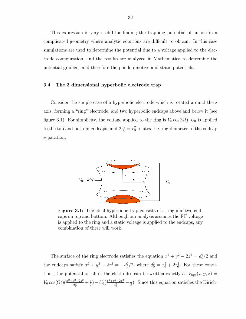
32
This expression is very useful for finding the trapping potential of an ion in a
complicated geometry where analytic solutions are difficult to obtain. In this case
simulations are used to determine the potential due to a voltage applied to the elec-
trode configuration, and the results are analyzed in Mathematica to determine the
potential gradient and therefore the ponderomotive and static potentials.
3.4 The 3 dimensional hyperbolic electrode trap
Consider the simple case of a hyperbolic electrode which is rotated around the z
axis, forming a “ring” electrode, and two hyperbolic endcaps above and below it (see
figure 3.1). For simplicity, the voltage applied to the ring is V0 cos(Ωt), U0 is applied
to the top and bottom endcaps, and 2z20 = r2
0 relates the ring diameter to the endcap
separation.
Figure 3.1: The ideal hyperbolic trap consists of a ring and two end-caps on top and bottom. Although our analysis assumes the RF voltageis applied to the ring and a static voltage is applied to the endcaps, anycombination of these will work.
The surface of the ring electrode satisfies the equation x2 + y2 − 2z2 = d20/2 and
the endcaps satisfy x2 + y2 − 2z2 = −d20/2, where d2
0 = r20 + 2z2
0 . For these condi-
tions, the potential on all of the electrodes can be written exactly as Vhyp(x, y, z) =
V0 cos(Ωt)(x2+y2−2z2
d20
+ 12)−U0(
x2+y2−2z2
d20
− 12). Since this equation satisfies the Dirich-

33
let boundary conditions on all of the electrodes, it is a solution for the voltage at all
points in space as well. The motion of the ion in one dimension can be found from
solving the separable equation ri = − em
(~∇V (r, t) · ri), where e is the charge of the ion
and ri is any coordinate direction. This gives us an equation of motion in the x, y,
and z directions of:
x +2e
md20
(V0 cos(Ωt)− U0)x = 0 (3.15)
y +2e
md20
(V0 cos(Ωt)− U0)y = 0 (3.16)
z − 4e
md20
(V0 cos(Ωt)− U0)z = 0 (3.17)
By transforming the equation of motion to the Mathieu equation of the type expressed
in 3.4, we arrive at the constants:
ax,y = − 8eU0
mΩ2d20
, qx,y = − 4eV0
mΩ2d20
(3.18)
az =16eU0
mΩ2d20
, qz =8eV0
mΩ2d20
(3.19)
Based on the relationship between ai and qi a diagram of the lowest stability
region can be generated (figure 3.2), where βi is real valued and between 0 and 1.
3.4.1 Ring and Fork Trap
Experimentally, this trap takes a slightly different form than the perfect hyperbolic
trap seen in figure 3.1, and is referred to as a “ring and fork” trap [35]. In our lab
we make these out of 125 µm thick molybdenum sheets, one with a hole (forming
the ring) and the other with a notch (the fork). This can be seen in figure 3.3.
Molybdenum is a good material for building ion traps because it is stiff, is a good
electrical conductor, and its native oxide has a work function which is very close to
the work function of molybdenum itself. This helps suppress electric field noise on
the electrodes, which we will be discussed in chapter 8.As one can see from the figure, this trap departs radically from a perfect hyperbola
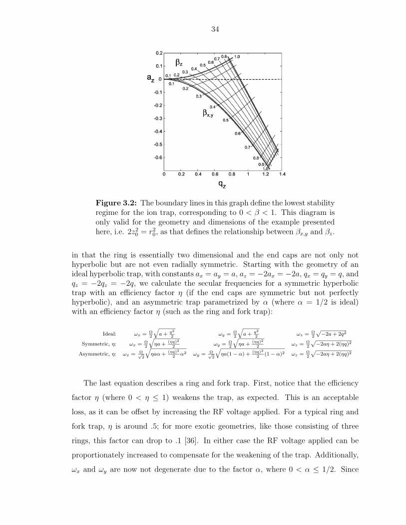
34
Figure 3.2: The boundary lines in this graph define the lowest stabilityregime for the ion trap, corresponding to 0 < β < 1. This diagram isonly valid for the geometry and dimensions of the example presentedhere, i.e. 2z2
0 = r20, as that defines the relationship between βx,y and βz.
in that the ring is essentially two dimensional and the end caps are not only nothyperbolic but are not even radially symmetric. Starting with the geometry of anideal hyperbolic trap, with constants ax = ay = a, az = −2ax = −2a, qx = qy = q, andqz = −2qz = −2q, we calculate the secular frequencies for a symmetric hyperbolictrap with an efficiency factor η (if the end caps are symmetric but not perfectlyhyperbolic), and an asymmetric trap parametrized by α (where α = 1/2 is ideal)with an efficiency factor η (such as the ring and fork trap):
Ideal: ωx = Ω2
qa + q2
2ωy = Ω
2
qa + q2
2ωz = Ω
2
p−2a + 2q2
Symmetric, η: ωx = Ω2
qηa +
(ηq)2
2ωy = Ω
2
qηa +
(ηq)2
2ωz = Ω
2
p−2aη + 2(ηq)2
Asymmetric, η: ωx = Ω√2
qηaα +
(ηq)2
2α2 ωy = Ω√
2
qηa(1− α) +
(ηq)2
2(1− α)2 ωz = Ω
2
p−2aη + 2(ηq)2
The last equation describes a ring and fork trap. First, notice that the efficiency
factor η (where 0 < η ≤ 1) weakens the trap, as expected. This is an acceptable
loss, as it can be offset by increasing the RF voltage applied. For a typical ring and
fork trap, η is around .5; for more exotic geometries, like those consisting of three
rings, this factor can drop to .1 [36]. In either case the RF voltage applied can be
proportionately increased to compensate for the weakening of the trap. Additionally,
ωx and ωy are now not degenerate due to the factor α, where 0 < α ≤ 1/2. Since

35
Figure 3.3: One easy experimental realization of a hyperbolic trap isthe ring and fork trap, consisting of a flat sheet with a hole cut in it andsurrounded on the top and bottom by “fork” endcaps. The voltagesapplied are shown in the diagram, with the low pass circuit on thefork electrode which serves to ground the RF potential but allow theapplication of a static voltage.
the fork end cap is straight, the axis parallel to the fork should be weaker in strength
than the axis perpendicular, and therefore ωx is designated as this direction. Breaking
this degeneracy is actually beneficial because it allows Doppler cooling in all three
dimensions with a single laser. As a simplified case, we see that the ring and fork
trap with U0 = 0 gives: ωx =√
2eηV0
mΩd20
α, ωy =√
2eηV0
mΩd20
(1 − α), and ωz = 2√
2eηV0
mΩd20
. The
x, y, z directions define the principal axes of the trap, which are the directions along
which the ion’s harmonic motion is uncoupled from the other directions. In the case
of the ring and fork trap it is straightforward to determine the principal axes, but
we will see later on that finding these axes in the case of two layer linear traps and
surface traps can often require the use of computer simulations.
In our lab we have used a ring and fork trap with a 200 µm radius and the fork
electrodes separated by 300 µm. By applying ∼400 volts of Ω/2π = 50 MHz RF
voltage to the ring, along with 30 volts on the endcaps, we can achieve a trap with
ωx/2π = 5.8 MHz, ωy/2π = 8.9 MHz, and ωz/2π = 9.7 MHz. From an experimental
standpoint, the static voltage is applied through a low pass filter to the endcaps. This
way the RF voltage is grounded via a capacitor, and the static voltage source does not
have a high, oscillating voltage being applied to its outputs. Additional compensating
electrodes are placed about 1 cm away from the trap to offset any bias electric fields
affecting the ion. Given they are so far away compared to the electrodes of the trap,
a few thousand volts are typically required to offset the background fields.

36
3.4.2 Needle trap
Another type of 3-D hyperbolic trap which will be discussed in greater detail later
in chapter 8 is the two needle trap (figure 3.4). This is like the hyperbolic trap but
without the ring, and is equivalent to the case where r0 →∞. It turns out that if the
needles are made pointy (with a radius of curvature small compared to the needle to
needle separation), the efficiency of this trap does not suffer too much compared to
the hyperbolic trap with a ring electrode. For the experiments performed here with
the needle trap, this efficiency was calculated to be η ∼ .17 over a 2z0 separation of
100 µmto 250 µm.
Figure 3.4: This geometry is related to the hyperbolic trap, wherethe endcaps are the needles and the radius of the ring r0 → ∞. Thisgeometry is very open optically, and subsequently is also very suscep-tible to bias electric fields. An experimental realization of this mightalso include grounded sleeves farther back on the needles which serveto mitigate the problem of stray bias fields.
When there are multiple ions in a 3-D ion trap, they line up along the weak
axis. This brings us to one of the main disadvantages of the 3-D hyperbolic trap
for experiments which require multiple ions (such as demonstrations of entanglement
or any other quantum computing application). When we have multiple ions, they
cannot all be at the single RF node, and therefore those that aren’t experience a
higher degree of micromotion which cannot be cooled. This motivates the building
of linear traps, which are discussed in the next section.

37
3.5 Linear traps
A linear ion trap refers to any ion trap in which the ponderomotive potential
only traps in two dimensions such that the RF node is a line. Static voltages are
used to confine the ions at specific points along this line. As mentioned above, this
has the benefit that if the secular frequency along the static axis is lower than the
ponderomotive secular frequency, then multiple ions will space themselves out along
this linear RF node but not experience excess micromotion, since they are still all at
the RF node. Three types of linear traps are shown in figure 3.5: a single layer trap
(a), a two layer trap (b), and a three layer trap (c). In each case the trap is shown
above, along with the static and RF potentials applied to the electrodes, and a plot
of the ponderomotive potential for a transverse cross section of the trap.
Figure 3.5: This figure shows three common types of linear trap: thea single layer trap, the b two layer trap, and the c three layer trap. Thestatic (U0) and RF (V0) voltages applied to the electrodes are written onthe top figure. Below each trap is a contour plot of the ponderomotivepotential resulting from that trap, calculated in CPO 3D. The darkerareas correspond to lower potential, and the white areas correspondto near the electrodes. The black dot in the middle of the electrodescorresponds to where an ion would be trapped.

38
3.5.1 Four rod trap
We will first look at the two layer trap, also referred to as a four rod trap, as it is
the easiest to analyze mathematically. The ideal instance of this is comprised of four
hyperbolic electrodes (see the cross section shown in figure 3.6).
Figure 3.6: This figure shows the transverse cross section of a linearhyperbolic trap, as well as the potentials applied to the electrodes. Thex′ and y′ axes correspond to the principal axes, in which the harmonicmotion of the ion is uncoupled.
The potential of a four rod trap with only RF voltage applied, expressed in regular,
rotated coordinates, and cylindrical coordinates is:
Vhyp(x, y) = −V0
r20
(xy) (3.20)
Vhyp(x′, y′) =
V0
2r20
(x′2 − y′2) (3.21)
Vhyp(r, θ′) =
V0
2r20
r2(cos2(θ)− sin2(θ)) =V0r
2
2r20
cos(2θ) (3.22)

39
where r0 is the distance from the ion to the nearest electrode and θ′ is the angle from
the positive x axis. Using the pseudo-potential approximation in equation 3.14 and
calculating the resultant secular frequency gives:
Ψhyp =e2V 2
0
4mΩ2r40
(x′2 + y′2) (3.23)
ωhyp =eV0√
2mΩr20
(3.24)
The stability diagram for this trap is shown in figure 3.7.
Figure 3.7: This graph shows the lowest stability region for a hyper-bolic linear trap. The βx and βy regions are symmetric because of thetrap’s symmetry about the RF node.
Much of the effort for this thesis was spent working on two layer microtraps,
which differ substantially from the ideal case in that the electrodes are not hyperbolic,
but are flat planes in which the vertical electrode separation is much smaller than
the lateral separation. Unlike the hyperbolic electrodes, they are not cylindrically
symmetric, although they do have a mirror symmetry across both the z=0 plane and

40
the x=0 plane. The difference between this and the ideal case can be parametrized
by decomposing the potential into an infinite series of cylindrical harmonics [37] and
calculating the voltage for the linear microtrap, Vlm:
Vlm = V0
[ ∞∑m=1
Cm(r/r0)mcos(mθ′) +
∞∑n=1
Sn(r/r0)nsin(nθ′)
](3.25)
Because the voltage is the same on diagonal electrodes and opposite on adjacent ones,
we only need to keep the terms which are the same when θ′ → θ′ + π and opposite
when θ′ → θ′ + π/2, i.e. m = 2, 6, 10 · · · and n = 4, 8, 12 · · · . These terms can be
found using numerical simulations, with the amplitudes of Cn and Sn (m, n ≥ 2)
quantifying the anharmonicity of the trap. Defining the distance to the electrodes as
l =√
(a/2)2 + (d/2)2 (where a and d are defined in figure 3.8), and comparing the
voltage of the linear microtrap to that of a four rod hyperbolic trap with r0 = l, we
define an efficiency factor and potential:
η =Vlm
Vhyp
=2C2l
2
r20
(3.26)
V(2)lm (x′, y′) =
V0η
2l2(x′2 − y′2) (3.27)
The resulting ponderomotive potential and transverse secular frequency is:
Ψ(2)lm =
e2V 20 η2
4mΩ2l4(x′2 + y′2)ωlm =
eV0η√2mΩl2
(3.28)
This equation shows that the ponderomotive potential at the trap axis is circular;
from numerical simulations we have found that it is approximately circular up to a
distance of a8, at which point C2 becomes significant. We have used several differ-
ent finite element modeling (FEM) packages to determine the trap’s anharmonicity,
including a 2-D solver in Matlab, Maxwell 3D from Ansoft, and Opera 3D from Vec-
torFields. For these simulations the geometry and voltages of the electrodes (and
sometimes the electrode material properties, such as permittivity and conductivity)
are defined, and a volume region of interest is defined which includes the trap location.

41
Figure 3.8: This trap is an experimental realization of a two layerlinear trap, behaving to first order like the hyperbolic trap describedabove. The picture of the electrodes shows different important dimen-sions. Below it is a transverse cross section superimposed on a diagramof the ponderomotive potential.
This region of interest is divided into tetrahedra, and the potential at each vertex is
calculated in an iterative process until they are internally consistent and consistent
with the boundary conditions set at the beginning. More recently we have used CPO
3D from Electronoptics, which is a boundary element modeling program (BEM) in
which the defined electrodes are divided into segments, and surface charges which are
evenly distributed over each segment are calculated to satisfy the boundary voltage
conditions. The potential at points in the region of interest are then simply calcu-
lated by summing the Coulomb potentials for each segment. This technique is much
faster and more accurate than the FEM solvers, and furthermore the potential can be
quickly recalculated when changing the voltage on an electrode by simply rescaling
the distributed charge.
In the specific case of the two layer gallium arsenide trap, whose fabrication details
will be discussed in section 6, we were initially concerned that the high aspect ratio
α = a/d would lead to a much weaker trap. This was investigated first with numerical
simulations using Maxwell 3D. From figure 3.9a, which graphs the efficiency factor η as
a function of α and for different values of δ = d/w, we see that the efficiency decreases
steeply after α = 1 but asymptotically approaches 1/π. The graph also shows that
the trap gets weaker for geometries with thinner electrodes. A similar plot (figure

42
(a) (b)
Figure 3.9: The graph in part a shows how the trap strength de-creases as the aspect ratio α (lateral separation of electrodes dividedby the vertical separation) increases. This quantity is parametrized byη, which equals 1 for an aspect ratio of 1 and asymptotically goes to1/π as α →∞. In part b we see that the maximum potential along aline perpendicular to the surface of the trap decreases with α, and seethat it too approaches an asymptotic value.
3.9b) shows how the potential depth in and out of the plane of the trap depends
on α. In traps which an “open” geometry, such as the two layer geometry shown
here with an open y direction and a confined x direction (because of the presence
of an electrode), the direction with lowest trap depth (not necessarily lowest secular
frequency) will be the open direction. While having a high secular frequency is good
for tightly confining an ion and performing fast gate operations (as will be described
later), from the standpoint of just trapping ions the important metric is the value
of the shallowest potential in a particular direction. Traps have been successfully
operated with minimum trap depths of between .08 eV (3 times room temperature)
and several eV (hundreds of times room temperature).
3.5.1.1 Modelling a two layer trap using conformal mapping
One can also calculate the effect of using planar electrodes instead of perfect hy-
perbolas using conformal mapping. This technique is generally useful for transforming
two dimensional problems in space to problems in the complex plane, as long as a

43
suitable mapping can be found. For our problem we adapted an analysis of fringe
fields in a parallel plate capacitor [38, 37] for a two layer ion trap with infinite plane,
zero width electrodes. In the complex plane this can be described as lines parallel
to the real axis starting at (±a/2,±d/2) and extending to (±∞,±d/2). These elec-
trodes then get mapped to a parallel plate capacitor,as seen in figure 3.10, and obey
the relationship:
±2wπ
d+
aπ
d− 1 = z + ez (3.29)
where the positive value of the first term is used for the electrodes on the left and the
negative value for the equations on the right. This transformation maps the original
electrodes to two infinite planes separated by 2π, where the potential in between is
that of a parallel plate capacitor, V = V0
2πIm(z). Different mapping functions must be
used so that the same voltage is applied on one side of the parallel plate capacitor. To
find the potential in the original problem the inverse of equation 3.29 must be solved
using the Lambert W function Wk(x), which obeys the equation z = Wk(z)eWk(z).
The inverse mapping is then z± = ζ± −Wk(eζ±), where ζ± = ±2wπ
d+ aπ
d− 1. The k
subscript in the Lambert W function signifies that we have to choose the appropriate
branch in the complex plane, and is given to us by [38] as k = d Im(ζ)−π2π
e. Now we have
z (the coordinates in the transformed, parallel plate capacitor frame) as a function of
w (the coordinates in the original two layer ion trap problem).
In the case of the GaAs trap discussed later, a d, which allows us to add the
solutions corresponding to the two different inverse transforms z± independently, as
we assume that since the opposite electrodes are so far away that they minimally
affect each other. Therefore we can write the original potential as a linear sum of
the two different sides of the ion trap, V = V0
2(Im(z+) + Im(z−)). The high aspect
ratio also allows us to make an approximation for the Lambert W function, since
ζ 1 → W0(ζ) ≈ lnζ− ln(lnζ). Inserting this into the mapping function above, and
we get z ≈ ln(ζ±). The resulting function can be expanded about w = 0 to:
z± = ln(aπ
d− 1) +
n=∞∑n=0
1
(−2)n(± 2πw
aπ − d)n+1 (3.30)

44
Figure 3.10: Using the technique of conformal mapping we can mapthe geometry of a two layer trap in the complex plane to a parallel platecapacitor, in which the voltage is known. The colors of the electrodesshow how they get mapped to the parallel plate capacitor.
When we plug this into the equation V = V0
2π(Im(z+) + Im(zi)), we see that all
even n terms cancel, and that the first term disappears because it is real valued:
V =V0
π
n=∞∑n=0
−2(−π
aπ − d)2n+2Im(w2n+2) (3.31)
Evaluating the above expression at w = x + iy gives:
V = − 4πV0
(aπ − d)2(xy + [3(x5y + y5x− 10x3y3] + · · · (3.32)
We can see from this that near the trap it is only necessary to keep the first
term, as the r2 term is large compared to the r6 term. Using the pseudo-potential
approximation (section 3.3), we find that:
Ψ =e2
4mΩ2(
4πV0
(aπ − d)2)2(x2 + y2) (3.33)
=e2V 2
0 η2
4mΩ2(x2 + y2) (3.34)

45
η =4π
(aπ − d)2l2 =
π(α2 + 1)
(απ − 1)2(3.35)
where l =√
(a/2)2 + (b/2)2 is the distance to the nearest electrode. Remember that
we assumed α 1, in which limit η → 1/π and agrees with the simulations above
as α → ∞. In [37] the trap depth is also calculated from this conformal mapping
solution, and the maximum trap depth is found at: rmax = a2(1− 1
πa):
Ψ(rmax) =e2V 2
0
4mΩ2
1
a2π2(1− 1/aπ)2(3.36)
where in the limiting case Ψ(rmax) → .23 [eV · µm2/V2] as α →∞.
3.5.1.2 Evaluation of the harmonic deviations
Returning to the analysis of the anharmonicities in the linear microtrap, we con-
cern ourselves primarily with the values of the first terms in the expansion 3.25 at
the trap center. This is plotted in figure 3.11, and it is apparent that for relatively
high aspect ratios (for the GaAs trap we demonstrated in chapter 6, α = 15), the an-
harmonicity is below a few percent. Also in the linear microtrap, the anharmonicities
grow at points farther from the center of the trap. This can be seen in figure 3.12.
One last concern with the ponderomotive potential is that linear traps are not
perfectly linear - real world implementations require gaps between adjacent electrodes
that can give rise to axial rf fields, and result in slightly trapping or anti-trapping
potentials along the rf node. While static fields will completely dominate this axial
potential, it is still a deleterious effect since the DC and RF axial minima might
not coincide, in which case the axial micromotion is non-zero. This effect can be
quantified by adding the term σz into the pseudo-potential equation Ψlm(x, y, z) =
e2V 20 η2
4mΩ2l4(x2+y2+σzz
2). From [37] this term was calculated for typical values of the gap
and electrode size, and found to be on the order of 10−13, and is therefore neglected
in future analysis.

46
Figure 3.11: This graph shows the first two anharmonic terms in thecylindrical expansion of the two layer trap, S4 and C6, as a function ofthe aspect ratio α. We can see that at worst they have a 4% and .2%effect. The coefficients are calculated for different values of δ = d/w.
3.5.1.3 Static confining potentials
Since linear traps require static fields in order to confine ions along the RF node,
we want to include those potentials in our analysis. It might seem that the effect of
static electrodes only needs to be analyzed along the axial direction, but by Gauss’
law we know that those electric field lines that converge at the trap center must be
radially anti-trapping, and therefore they partially cancel the ponderomotive poten-
tial. Therefore it is important to have a feeling for their effect in all directions so that
the competing interests of a having a strong radial trap and a strong axial trap are

47
Figure 3.12: This graph shows how the trap gets more anharmonicfarther from the center of the trap, parametrized as r0/(a/2), wherea/2 ≈ the distance from the ion to the electrode for high aspect ratiotraps.
met.
From figure 3.8, we simulate a trap with U0 volts applied to the end cap electrodes,
and then find the potential U(x, y, z) around the trap center (0, 0, 0). The static
potential can then be parametrized by
Ulm =U0
2(Dxx
2 + Dyy2 + Dzz
2) (3.37)
where
Dx =1
U0
∂2Ulm
∂x2(0, 0, 0) (3.38)
Dy =1
U0
∂2Ulm
∂y2(0, 0, 0) (3.39)
Dz =1
U0
∂2Ulm
∂z2(0, 0, 0) (3.40)
These constants obey the relation that Dx + Dy + Dz = 0, and since we know
that Dz > 0, we know that either Dx < 0 and/or Dy < 0. Along the axial z direction

48
we see that the secular frequency will be√
DzU0em
. The total potential and secular
frequency in each direction is then:
Φlm = Ψlm + Ulm (3.41)
=e2V 2
0 η2
4mΩ2l4(x2 + y2) +
U0
2(Dxx
2 + Dyy2 + Dzz
2) (3.42)
so that
ωlm,x =
√e2V 2
0 η2
2m2Ω2l4+
DxU0e
m(3.43)
ωlm,y =
√e2V 2
0 η2
2m2Ω2l4+
DyU0e
m(3.44)
ωlm,z =
√DzU0e
m(3.45)
3.5.1.4 Principal axes
Finding the principal axes of the two layer linear ion trap require the use of sim-
ulations. We can see that for the case where U0 = 0, when only the ponderomotive
potential plays a role, the transverse principal axes are degenerate. A small static
voltage applied (such that ωx′ ≈ ωy′) to the RF electrodes would break this degen-
eracy, resulting in principal axes in the z, 1√2(x + y), and 1√
2(x− y) directions. This
can be seen from considering the perfect hyperbolic four rod trap which would have
the same transverse principal axes at angles 45 and −45 from the y direction, and
realizing that it is a first order approximation to the linear microtrap at the RF node.
To find the principal axes when we apply larger static voltages, we calculate
the Hessian matrix at the center of the trap from simulations, and then find the
eigenvalues of the matrix, which denote the principal axes. We show this by example.
If static voltages are applied which break the degeneracy, the potential contours are
elliptical. For the case of principal axes in the x and y directions, an equation of the
form Φ ∝ x2
a2 + y2
b2, where a > b, would describe a trap with ωx < ωy. If we rotate
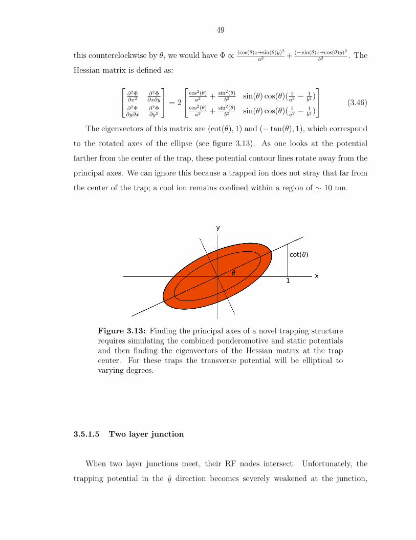
49
this counterclockwise by θ, we would have Φ ∝ (cos(θ)x+sin(θ)y)2
a2 + (− sin(θ)x+cos(θ)y)2
b2. The
Hessian matrix is defined as:
∂2Φ∂x2
∂2Φ∂x∂y
∂2Φ∂y∂x
∂2Φ∂y2
= 2
cos2(θ)a2 + sin2(θ)
b2sin(θ) cos(θ)( 1
a2 − 1b2
)
cos2(θ)a2 + sin2(θ)
b2sin(θ) cos(θ)( 1
a2 − 1b2
)
(3.46)
The eigenvectors of this matrix are (cot(θ), 1) and (− tan(θ), 1), which correspond
to the rotated axes of the ellipse (see figure 3.13). As one looks at the potential
farther from the center of the trap, these potential contour lines rotate away from the
principal axes. We can ignore this because a trapped ion does not stray that far from
the center of the trap; a cool ion remains confined within a region of ∼ 10 nm.
Figure 3.13: Finding the principal axes of a novel trapping structurerequires simulating the combined ponderomotive and static potentialsand then finding the eigenvectors of the Hessian matrix at the trapcenter. For these traps the transverse potential will be elliptical tovarying degrees.
3.5.1.5 Two layer junction
When two layer junctions meet, their RF nodes intersect. Unfortunately, the
trapping potential in the y direction becomes severely weakened at the junction,

50
so as to make an unmodified two layer trap impractical as an architecture for an
array of traps in which shuttling ions is possible. This can be seen qualitatively
by modeling a two layer junction as a hyperbolic electrode in each of the 8 octants
of three dimensional space, with (0,0,0) being the junction, and each neighboring
electrode having the opposite RF voltage. The potential in the trap is then Φ ∝ xyz,
so the ponderomotive potential at the junction is Ψ ∝ |∇Φ|2 = (xy)2 + (yz)2 + (xz)2.
Along any of the axes the potential is a constant 0, and so there is no trap preventing
the ion from escaping out of the top and bottom. This is an obvious result; in the
case of the hyperbolic junction the vertical axis is equivalent to the two lateral axes,
which don’t have axial pseudo-potentials either. It should also be noted that this is
not necessarily a good approximation to a two layer trap with flat electrodes. Indeed,
if we run a computer simulation we see that there is a non-zero trapping potential in
the vertical dimension due to the anharmonicities of the potential, and so in principal
we could have a junction trap with this geometry. As we will see in a later chapter
about the T-trap, the task of shuttling an ion through a junction is difficult enough
without the trap being really weak in addition.
One solution to this problem is to add bridges between the RF electrodes in
the junction region, a technique which is being tried by the NIST group [39]. By
“plugging” the RF hole (see figure 3.14) with bridges, they are able to maintain a
strong trap even in the junction region. Their trap is fabricated by electroplating gold
on an alumina substrate, and then aligning the vertical layers together. While this is
a good way to extend the two layer trap for shuttling purposes, it is mostly limited
to manually assembled traps, as the criss crossing bridges cannot be implemented in
most lithographically fabricated traps (an exception is the polysilicon trap discussed
later).
3.5.2 Single layer trap
The single layer trap is similar to the two layer trap, but with all of the electrodes
moved into the same plane (figure 3.15). One nice feature of this trap is the ease

51
Figure 3.14: Two layer traps do not have a ponderomotive verti-cal trapping component at a junction. A solution to getting aroundthis problem is to connect diagonal RF electrodes with bridges at thejunction. This technique of capping the ponderomotive hole in the ver-tical dimension is being tried at NIST for a trap with a junction andextended linear region.
of fabrication. Many fabrication woes arise from having multiple layers - such as
increased capacitance and voltage breakdown problems. Also, the traditional strength
of semiconductor fabrication lies in the lateral flexibility of lithography, while vertical
structure and machining tend to be more difficult. Another nice feature of this trap
is that it maintains a ponderomotive trap at a junction, as opposed to its two layer
relative. This particular layout will be discussed in more detail in section 7.2.
The single layer four rod geometry can be implemented with either two RF wires
surrounding the center of the trap or with an RF and a DC on either side, as seen
in the transverse dimensions in figure 3.15. In the first case, the trap center lies
symmetrically between the RF electrodes, while in the second case there are two
trap centers, one above the plane of the trap and one below, as determined by the
wire diameter and spacing. This second case is compared with a two layer trap in
[39] using complex variables and line charges to arrive at an analytic solution for the
ponderomotive potential.

52
Figure 3.15: In this figure we see two different types of single layertrap geometries. In part a we see one with RF electrodes surroundingthe RF nodal axis, denoted by an “x”. The Sandia trap discussed insection 7.2 is of this type. In part b there is a trap with the samegeometry, but with alternating wires of RF and static voltages. In thiscase there are two nodal axes, above and below the plane of the trap.This is similar to the surface trap which will be discussed later, butwith two allowed RF nodes.
3.5.3 Three layer trap
The three layer trap (figure 3.16) has been used extensively in my lab for a variety
of experiments, from demonstrating Grover’s algorithm to shuttling an ion around
a corner. From a geometric point of view, the three layer trap has the advantage
that junctions are possible with it and that micromotion can easily be compensated
in all three directions for each individual set of electrodes. The downsides are that
compared to a two layer trap the trap depth is weaker given the same voltage and
distance from the ion to the electrode, and it is slightly more difficult to build, due
to the extra layer. This geometry will be discussed more extensively in chapter 5.
3.6 The surface trap

53
Figure 3.16: This cross section shows a three layer trap with angledelectrodes, similar to the gold-on-alumina T trap. The middle elec-trodes have RF applied to them and the top and bottom electrodes areRF grounded and segmented so they can have static voltages applied.The three layer trap is particularly suited for compensating micromo-tion in each segment of the trap.
A special type of linear trap is the surface trap. It differs from the three types of
linear traps listed above (except the single layer wire trap with alternating RF and
DC electrodes) in that its electrodes are not placed symmetrically about the linear RF
node. As seen in figure 3.17, the RF node lies above the plane of electrodes, requiring
that either backside holes be etched for laser access or lasers be brought across the
surface. It offers the possibility of easy fabrication and also eliminates a topological
problem with “through traps” in which the laser is brought through a hole in the
substrate. The problem with through traps is that if they are part of a large array
with many junctions, there will be islands of disconnected trap electrodes. A possible
solution for through traps would be to etch areas under the electrodes which allow for
ion trapping but do not have a through hole allowing laser access. The surface trap
gets around this by trapping the ions above the surface. As a downside, however,
one must be more careful not to illuminate ions other than the intended ones. One
design consideration for the surface trap is that the principal axes must be rotated so
that one axis is not perpendicular to the surface of the trap (see figure 3.17). In the
case where laser cooling beams come across the surface of the trap, the ion cannot
be cooled if one of its principal axes is perpendicular to the surface and therefore the
cooling beam.
3.7 Computer simulations of electric fields from electrodes
As mentioned previously, CPO 3D was used for most of the simulations performed
in the course of this thesis research. While the design interface is somewhat clunky

54
Figure 3.17: Surface trapThree types of surface traps are shown here, along with the position and principal axesdirections denoted by an “X”. In part a the trap comprises two RF electrodes placedon either side of a center DC electrode, around which are two more DC electrodes.With zero volts on the DC electrodes this would give us a principal axis perpendicularto the surface of the trap, but this can be rotated by applying an appropriate amountof DC voltage. Part b offers another solution to the principal axis problem by makingthe RF electrodes different widths. Part c solves the problem by having four electrodesinstead of five, breaking the symmetry and therefore having principal axes at 45 degto the perpendicular of the trap.
until one gets used to it (see figure 3.18), the speed and accuracy of the simulations
makes up for this deficiency. A few examples of simulations are shown in figures
3.19, 3.20, and 3.7. While analytic solutions are available in many cases of linear
and surface traps [39], the flexibility of a simulation often makes it more practical for
complicated geometries which lack symmetry. Analytic solutions, on the other hand,
are particularly useful for problems which require minimizing a certain parameter,
such as the change in the secular frequency with ion position ([40], section 7.1).
Otherwise a simulation would require a trial and error approach to find a solution.
CPO can output the electric field or electric potential on a 2D or 3D grid. We typ-
ically used two dimensional arrays of data in the transverse plane and one of the axial
planes. A set of “basis” static potentials for each electrode was compiled by applying
one volt to a particular electrode, grounding the rest, and outputting the potential

55
in the plane of interest. This was repeated for each electrode (taking advantage of
symmetry to reduce the number of simulations when possible), allowing a total static
potential to be calculated from the linear sum of these, with coefficients depending
on the voltage applied. The ponderomotive potential was calculated by applying one
volt to the RF electrodes in the simulation and then outputting the electric field on
a grid and solving the pseudo-potential equation 3.14 (the micromotion component
is ignored). This was then scaled by V 2 for the case of different voltages and added
to the static potential solution to find the total potential of the ion. Intermediate
potential values between the grid point are determined using Mathematica’s Interpo-
lation function. A more detailed description of how the CPO data is actually used
can be found in section 7.1.

56
Figure 3.18: The CPO user interface for defining electrode geometriesconsists of a library of standard three dimensional shapes (including twodimensional surfaces) which can be tailored to a particular electrodegeometry. This example shows a flat electrode parallel to the z plane,with the (x,y) coordinates of two corners specified. The ”numbers of 2applied voltages” line specifies the address of the voltage applied to theentire electrode, which is defined in another dialog box. The ”total nrof subdivs” line specifies how CPO should subdivide the electrode intoregions; each of these regions will have a distributed charge. Havingmore regions increases the accuracy of the simulation, but also increasesthe computing time required to arrive a solution.

57
Figure 3.19: This is an overhead view of a surface trap modeled inCPO. The outside squares are static control electrodes, the long rect-angular electrodes are the RF electrodes (which are raised 10 µmabovethe surface of the trap, and the central electrode is for applying staticvoltages.
Figure 3.20: This linear ion trap consists of segmented rectangularelectrodes at 90 to form a linear trap. The distance from the electrodeedge to its neighbor is 2 mm, allowing for clear optical access for MOTcooling beams for a neutral trap. CPO was a useful tool in this situationbecause it gave an accurate prediction for the amount of RF and endcap static voltages necessary to have a particular strength trap.

58
Figure 3.21: This trap is an example of a more elaborate design fora surface trap junction. Computer simulations are particularly usefulin the cases of traps without a simple symmetry, as is the case here.In this idea, the triangular electrodes at the junction are static controlelectrodes which can be switched according to which way the ion ismeant to turn. The three rectangular electrodes on the sides of thecentral triangle are switchable between DC and RF voltage dependingon the direction the ion needs to be shuttled.

CHAPTER 4
Experimental setup
This chapter will detail the main components of our experimental setup, many of
which are common to all trapped ion experiments.
4.1 Achieving ultra high vacuum (UHV)
Our vacuum chambers (see figure 4.1) are operated at UHV pressures, ideally
below 10−11 torr. This level of vacuum is achieved by using only UHV compatible
materials, primarily stainless steel (316 or 304), tungsten, oxygen free copper, gold,
quartz, fused silica, kapton insulated wire, ceramics, Vespel SP3, and PEEK, along
with a variety of other specialized materials. If screws with blind holes are used,
notches are cut in the threads to prevent virtual leaks from the trapped volume. All
of the parts are cleaned in an ultrasonic acetone bath and rinsed with methanol and
sometimes isopropyl alcohol. Powder free latex gloves are used at all times when
handling vacuum components that are going in the chamber. All solid stainless steel
parts (not viewports or feedthroughs) are prebaked at 400 for a few days to form
an oxide on the stainless steel which limits outgassing.
4.2 The bake
The pump-out occurs in multiple stages. First the air in the chamber is evacuated
with a turbopump (Pfeiffer TSU 071) down to about 10−6 torr. All of the components
which will have high current running through them during normal operation (such
59

60
Figure 4.1: This picture shows a typical vacuum chamber consistingof a hemisphere (or spherical octagon) which holds the ion trap itself,a titanium sublimation pump, and an ion pump. Other componentsthat are not labelled here include the bakeable valve, the viewports forlaser beam access, and the feedthroughs for electrical interconnects.
as the oven filaments, the ion gauge filament, and the titanium sublimation pump
filaments) are degassed at a lower current for a short period of time (for instance,
the Ti-Sub pump filament is run at 35 amps for 20 minutes). After this we begin the
bakeout in an industrial oven which allows for even heating of the chamber without
using heater tape. The oven is initially turned on at 200 F and brought up a
maximum of 30 F every three hours. At 230 F the valve connecting the chamber to
a 500 L/s ion pump (Perkin Elmer 500 STP) is opened, and the valve connecting the
turbopump is then closed. The temperature ramp is continued at the same rate till
392 F (200 is reached, and the pressure on the ion gauge monitored for the next
few days. This maximum temperature is set by the maximum bake temperature on
the fused silica/quartz windows (MDC 450020), and in particular the PbAg brazing
used to seal the viewport to the stainless steel. These windows are chosen for their
relatively high (∼90%) transmission at 214 nm when anti-reflection coated. Otherwise
sapphire windows which can be baked to 400 would have been used. When the
pressure bottoms out (typically in the high 10−8 to low 10−7 torr), the 20 L/s internal

61
ion pump (Varian Starcell) is turned on, and the bakeable valve that connects both
the 500 L/s ion pump and the turbopump is hand tightened. It is important not
to tighten it so hard that it deforms the copper gasket inside. The 500 L/s pump
remains pumping the other side of the bakeable valve. After a few more days at 392
F the pressure bottoms out to the high 10−9 to low 10−8 torr and the temperature
is ramped down by about 30 every three hours. Once the chamber reaches room
temperature the bakeable valve is tightened to the prescribed torque with a torque
wrench (the torque is increased 2 ft-lb’s after every bake), with the 20 L/s pump left
running continuosly. Finally, the titanium sublimation pump is run usually 10 - 20
times for 2 minutes each at 45 amps till the pressure decreases to below 10−11 torr.
The whole process typically takes a week.
If the chamber does not pump down to this level, there is either a non-UHV
compatible part inside or a leak on the outside. The outside leak is the easiest to
diagnose, and if the culprit can be identified to be a viewport (which it usually is)
the offending part can be replaced quickly and the bakeout repeated in about half the
time as before (as it was not exposed to the air for long). If the pressure is greater
than ∼ 5× 10⁻¹⁰ torr, it can be found either by blowing helium around the chamber
and looking for a spike in the pressure or squirting acetone around the gaskets and
looking for a drop in pressure (as the acetone plugs the leaks). If the leak is lower
than ∼ 5 × 10⁻¹⁰, it might be necessary to squirt methanol around the gaskets and
wait for 10 - 20 minutes to see if the pressure decreases. Leaks this small are difficult
to see with the acetone and helium tests, as the acetone evaporates too quickly to
see an effect and the helium would have to be directed at the same spot for several
minutes to register on the pressure gauge.
4.3 The chamber
Our chambers are constructed with off-the-shelf confocal flat components from
Kimball physics and viewports from MDC. Our machine shop has also made some
custom pieces for us requiring titanium alloy welding. As mentioned above, each

62
chamber has a 20 L/s ion pump which runs continuously, and a titanium sublimation
pump which is run intermitantly as needed. For the part of the chamber in which
the ion trap is contained we have used a single Magdeburg hemisphere (MCF450-
MH10204/8), a Magdeburg hemisphere plus a spherical octagon, and a single large
spherical octagon (MCF600-SO200800) from Kimball physics. In all of these cases
the largest available viewport was used for imaging and the others for laser access.
For traps which require fewer than ∼ 30 DC control voltages, MDC multipin
instrumentation feedthroughs are used, which can have between 2 and 35 pins which
connect to push on connectors. A two pin high voltage version of this feedthrough is
used for the RF electrodes in all of the chambers. For the semiconductor fabricated
microtraps, more control electrodes are needed, and so the type D instrumentation
series connectors were chosen, with PEEK ribbon connectors and Kapton coated wires
used for connections inside the chamber.
The microtraps impose some fairly exotic requirements on the chamber, given the
number of leads and the need to swap new traps in and out of the chamber. For
this task we chose to use a 100 pin CPGA (ceramic pin grid array) from Global
Chip Materials (PGA10050001) to attach the ion traps; 50 of those pins were hooked
to DC control signals and 2 to RF. The other pins remained empty. The socket
they were plugged into was made out of Vespel SP3, a UHV compatible plastic from
Dupont, although other groups have had success with PEEK as well. This is an easily
machinable material (see the technical drawing for this in figure 4.3) which offers good
mechanical stability for the socket. Gold plated recepticles were used to connect to the
pins on the CPGA (part number 0672-4-15-15-30-27-100 from PCS Electronics). Due
to the initial dificulty of pushing the CPGA into them, each recepticle was “annealed”
with a .016 inch diameter stainless steel wire in them at 450 for 1.5 minutes. They
were placed on a ceramic plate which sat on a nichrome wire in a nitrogen purged
box. After this process the recepticles were strong enough to make repeatedly good
contact but not so hard that they were dificult to put on. They were then crimped to
the Kapton coated wire with a Paladin PA1440 crimper. The entire socket and chip
carrier assembly, along with its mounting block and ovens, can be seen in figure 4.3.

63
Figure 4.2: This figure (courtesy of Jon Sterk) shows the physicaldimensions of the custom made socket used for connecting to the 100pin CPGA chip carrier. It was fabricated out of Vespel SP3, which waschosen for its strength, flexibility, RF properties, and UHV compatibil-ity. Two of these pieces would be used to sandwich 50 recepticles forcontacting the CPGA pins (the other pins were not hooked up).
These components were mounted in the chamber with custom made brackets and
groove grabbers from Kimball physics (see figure 4.3). The trap when attached to
the CPGA sat less than 5 mm from the inside surface of the viewport. Depending
on the trap, a hole could be drilled in the back of the ceramic chip carrier for optical
access from the backside.
4.4 RF resonator
High voltage (100 V - 2000 V) is delivered to the trap via an HP 8640 function

64
Figure 4.3: This figure shows the entire UHV compatible CPGAsocket assembly and mounting block. The exploded view at the bot-tom right shows the chip carrier going into the vespel sockets, whichsandwith 50 recepticles between them (shown in gray). The socketsconnect to a mounting assembly which also holds the Cd ovens andmounts to the vacuum chamber via groove grabbers.
generator, an RF power amplifier, and an RF resonator used for impedence matching
the trap (an open circuit with some capacitance to ground) to the power source. Since
the circuit is open and there is little current flowing (depending on the capacitance),
the loaded Q can be quite high, and so deliver a high voltage to the trap with minimal
input power. There are multiple kinds of RF resonators, one of which is the coaxial
variety consisting of a single wire in the middle of a conducting can. An antenna at
the bottom (opposite the load) which is oriented so as to generate magnetic fields
circularly about the central wire is used to couple RF power into the resonator. The
resonant frequency of this apparatus is λ/4 = length of the inner wire. At 50 MHz, the

65
Figure 4.4: This overhead view of the vacuum chamber shows thelaser access to the ion trap which is afforded by the 1 1/3 inch viewportsthat are at 60 to the large 4.5 viewport normal. A 4.5 inch sphericaloctagon is attached to the front (top in the picture) of the hemisphereso that the reentrant viewport used for imaging can be close to thetrap, and to add extra room for mounting structures and wires.
frequency we usually operate our ion traps at, a 1.5 m inner wire would be required,
which is unwieldy and impractical. Instead we use a helical coil, as described in
[41] and figure 4.4. This uses a coiled inner copper wire with a copper outside can,
where λ/4 is roughly the length of the coil, but also depends on a number of other
parameters, such as the diamater of the coil, the gauge of the wire, and the diameter
of the can. We typically use a 3 inch copper pipe for the can and make the helical
coil out of 10 gauge copper wire, which is coiled about 10 times with a diameter of
about 1.5 inches. Power is coupled into the can with an antenna at the top such
that the magnetic field generated will circle around the wire coil. These resonators
typically have loaded Q’s of between 300 and 500, and the voltage on the trap is
then V = 20√
PQ, where the constant 20 is dependent on the exact geometry of the
resonator. The Q can be increased by cleaning the inside of the copper can, as dirt
inside increases power loss. The resonator is critically coupled to the trap by moving
the antenna in and out till the reflection disappears on resonance.
Sometimes a DC bias needs to be applied to the RF. In that case, the top end of

66
the coil, which is usually capped with a BNC and grounded to the can, has a low pass
π filter attached to it. At this point a static voltage can be applied without affecting
the Q, as long as the capacitor is high enough ≥ .1µF that the RF is effectively
grounded here. There are also times when two signals with the same RF but different
static voltages need to be applied to the trap. In this case we make a bifilar resonator
consisting of two coils which run right next to each other inside the resonator can.
This is made easier if we use a piece of teflon with holes drilled in it to space out and
support the two separate coils; otherwise it is difficult to keep them from shorting to
each other. The teflon does not significantly hurt the Q of the cavity. We put a large
(≥ 1µF) capacitor between them at the output to ensure that the phases of RF are
the same. Two separate π filters can then be attached to the opposite ends of the
coils.
RF power can also be coupled into the resonator capacitively. By attaching a
variable capacitor near the output of the helical coil and applying RF voltage at the
can’s resonant frequency the trap can be impedance matched to the RF source. The
resonator is critically coupled by tuning the variable capacitor. This type of resonator
was used for the GaAs trap, with an additional variable capacitor attached across the
output leads to allow for tuning the resonant frequency. The GaAs trap was unique in
that it could only tolerate 10 - 15 volts RF and had high loss and a subsequently low
(∼ 50) unloaded Q. The RF could have been applied without a resonator, but it was
useful because the trap was operating on the edge of its tolerable voltages, so that if
the trap itself heated up from power dissipation the resistance of the GaAs changed
and the cavity drifted off of resonance. This would reflect some of the power back to
the RF source and lower the voltage across the trap, protecting it from catastrophic
voltage breakdown.
4.5 Ovens
A vapor of neutral cadmium is generated by heating an atomic source (either a
single isotope or natural source) in an oven which is generally pointed at the trap

67
Figure 4.5: Part a diagrams a schematic of the cavity resonator usedto impedance match the trap to the amplified RF source, without whichmost of the power would be reflected or go into heating a parallel 50Ω resistor. In the schematic we see the RF source at the top drivinga “pigtail” coil. The magnetic fields generated by this pigtail coupleinto the larger coil and produce high RF voltages at the bottom, whenthe drive frequency is on resonance. The outputs of the resonator arethe RF high wire and a grounded wire, which is shorted to the outsideof the resonator. The upper part of the main coil is RF grounded tothe can. By attaching a π filter we can apply a DC bias to the RF hiwhich does not significantly effect the Q of the resonator. In part b wesee an actual resonator, made from a section of 3 inch diameter copperpipe, endcaps, and a coil of 10 gauge copper wire. The copper shouldbe polished with a brillo pad or stainless steel, or even chemically withhydrochloric or phosphoric acid, to improve the Q and minimize RF losson the inside of the can. All open holes in the can should be coveredwith copper tape.
region. Our early experiments used metallic Cd packed in an oven made of a stainless
steel tube with one end open. The tube was heated by running current through it,
which was sufficient to vaporize the Cd (boiling point 769 at 1 atmosphere). The
downside to this method was that during the 200 bakeout the metallic Cd would
coat the inside of the chamber, giving the gold trap electrodes a dull metallic tinge.
In the worst case this can short out electrodes, and is of a particular concern for small
traps in which the distance between adjacent electrodes is short. It is also blamed for
increasing the electric field noise coming from the trap electrodes [42].

68
Over the course of building several Cd traps it was realized that firing the ovens
was not necessary for trapping. The room temperature partial pressure of Cd is
∼ 10−13 torr, just below the base pressure of the vacuum chamber. This is ideal from
a trapping standpoint; for most of our strong traps, once we got them working the
first time and aligned the lasers and imaging optics, we never had to fire the ovens
again, relying on the background vapor pressure to load from. This made Cd well
suited for testing shallow traps, since we did not need a directed source of Cd targeted
at the trapping region which could contaminate or short the electrodes.
In more recent traps we have substituted metallic cadmium for cadmium oxide.
With a much higer boiling point (1559), the CdO does not contaminate the chamber
during the bakeout. It does require a hotter oven to generate the initial Cd vapor,
but once that has been achieved, it is similar to the metallic sources in that we do
not have to fire the ovens and can just load from the vapor. This hotter oven (see
figure 4.5) consists of a ceramic tube about .1 in in diameter with tungsten filament
wrapped around it. The CdO is packed in the tube, which is sealed at one end with
either uranium glass or a ceramic paste, and a smaller aperture is pasted to the other
end. This prevents the CdO from hardening while it is heated and shooting out of the
oven like a bullet. By running about 1 amp through the 10 - 20 coils of tungsten wire
we can get a significant amount of Cd vapor. The ovens (both metallic and oxide)
were tested in a bell jar to find both the current which produces a visible spot on the
glass and also the current at which the residual gas analyzer registers a noticeable
increase in Cd vapor (∼ 10−9 torr). When working with cadmium, particularly the
oxide whose particulate constituents can easily be breathed in, it is important to wear
personal protective equipment like gloves and a HEPA air filter mask. Cadmium is a
known carcinogen which is highly toxic if one is exposed to high doses.
4.6 Photoionization
Before we used photoionization of the neutral Cd vapor, electron guns consisting of
a negatively biased filament (∼ 100V ) through which current was run and a grounded

69
Figure 4.6: This figure shows two cadmium ovens, made out of aceramic tube with tungsten wire coiled around each tube for heatingthem. The red material seen on the inside is cadmium oxide. Typicallyan oven like this would also have a small ceramic aperture at the frontto make sure the cadmium oxide does not fall out.
accelerator plate were used to direct a stream of ionizing electrons into the trapping
region. While ultimately effective, this method was inefficient, ionized all particles
including air molecules, and contaminated the system and raised the ambient pressure.
Replacing this with a photoionizing laser improved performance in all these areas. By
focusing the a pulsed photoionization beam in the trapping region, all isotopes and
velocity classes of Cd can be ionized and the loading rate increased to above 1 s−1
[43].
In Cd, the ionization process requires a two photon transition from the 5s1S0 →
5s5p1P1 state and then to the continuum (see figure 4.6), where the photoionization
excites the ion 1.84 eV above the threshold. This scheme can be generally applied to
many of the other ion QC candidates, including Be, Ca, Sr, Ba, Mg, Yb, and Zn, with
the exception of Hg which would require a 185 nm laser. The flux of photoionized
atoms is determined from the number of atoms in the focus of the beam at the location
of the trap, the size and depth of the trap, the time required for a π Rabi rotation
from the ground state to the intermediate state due to the photoionization beam, and
the probability of the transition to the continuum based on the cross section of the
intermediate 1P1 state. Both the pulsed beam and the detection beam can be used
to excite the ion from the intermediary 1P1 to the continuum, but the higher peak
intensity of the pulsed laser makes it the dominant contributer. The final loading rate
is calculated to be ∼ 4s−1 for our laser setup, which is consistent with observations.

70
We use a mode-locked Ti-sapphire laser centered at ∼ 915 nm with a ∼ 10 nm
bandwidth that produces 100 fs pulses at an 86 MHz repetition rate. The Ti-sapphire
is pumped with 4.7 - 5 W of 532 nm light from a Spectra-Physics Millenia pump laser,
and requires excellent thermal contact and cooling in order to run at this wavelength,
due to the high gain in this region. A pair of Brewster cut fused silica prisms are used
to compensate for the group velocity dispersion, and the laser is tuned by cutting off
a portion of the separated spectrum after the prisms. The output light is frequency
doubled first by focusing through a 7 mm long LBO crystal and then doubled again
through a 5 mm long BBO crystal. Both are crytically phase matched through
angle tuning. The final output power ranges from 4.5 mW to 6.5 mW. The output
beam is highly astigmatic and slightly elliptical; we tried correcting for this with an
anamorphic prism pair and cylindrical lenses, but found that the best way to get a
tight focus at the trap was to minimize the distance from the doubling crystals to the
trap.
4.7 Lasers and frequency modulation
While cadmium is an excellent qubit choice from an atomic physics perspective,
it is technically difficult due to its short wavelength UV transitions. Most of that
hardship therefore falls on the laser and frequency modulation systems. For the
trap development experiments we need a detection/cooling beam at 214.5 nm, an
initialization beam (which uses the cooling beam), a Raman transition beam (whose
wavelength choice depends on the output power but which we detuned by 70 GHz from
the 2S1/2 −2 P3/2 transition), and a photoionization beam at 228.9 nm, as described
in the section above.
The detection and cooling beams come from the same laser (see figure 4.7); they
differ only in the frequency applied to the AOM. The cooling beam is most efficient
at a quarter linewidth below the atomic transition, while the detection beam is most
efficient at the peak of the atomic transition. They both use the same AOM, and are
switched via an RF switch that changes the frequency source from a 185 MHz source

71
Figure 4.7: This diagram of the photoionization energy levels showsthe two photon process which excites an electron from its ground state5S1S0 ground state level to the intermediate 5s5p1P1 level and then upto the continuum. The first transition can be excited with the pulsedlaser, while the second can be excited by either the pulse laser or theCW cooling laser, although the much higher intensity of the pulsedlaser makes it the dominant contributer to this process.
(cooling) to a 200 MHz source (detection) as needed. The laser itself is a Toptica TA
100 continuous wave diode laser which goes through a tapered amplifier to produce
∼ 700 mW of tunable power. This goes into a Toptica SHG 110 cavity which uses
an LBO crystal for second harmonic generation, which puts out ∼110 mW of 429
nm laser power. An EOM after the first doubler puts on 6.85 GHz sidebands, which
are doubled to 13.7 GHz in order to pump the 111 isotope out of its dark state via
the 2P3/2 F=1 state. The last stage is a Wavetrain CW frequency doubling cavity
from Spectra-Physics, which uses a temperature controlled BBO crystal to generate
∼ 1 mW of 214.5 nm light. The output of this goes into a AOM which splits the
beam into a cooling/detection part and an initialization part. Since the initialization
beam is tuned between the 2P3/2 F=2 and F=1 levels, it must go through a double
pass AOM at 400 MHz; since it is already 200 MHz below the cycling transition, an
additional 800 MHz puts it 600 MHz above the F=2 transition. This corresponds
to the maximum initialization efficiency. The cooling/detection beam gets upshifted
72
by 185 or 200 MHz out of the AOM, depending on whether the cooling or detecting
portion of the experiment is run. It also goes through a polarizer and quarter wave
plate so that only σ+ light is generated for the cycling transition.
In between the two doublers in the Doppler cooling beam path is a tellurium vapor
cell used to lock the frequency of the doubling lasers, compensating for frequency shifts
due to mechanical vibrations or temperature drifts. Locking this laser is important
for accurate measurement of the cadmium lineshape and for having efficient detection
of the qubit state. The 130Te2 cell is wrapped in heater tape to keep the cell at ∼
470 and further wrapped in insulation to minimize temperature gradients. About
5 mW of power from the blue light coming out of the first doubler is diverted into a
double pass AOM (Brimrose TEF-1000-300-429) at 900 MHz to match the difference
in the 2S1/2 →2 P3/2 (the negative first order is used). This beam then gets split into
a pump beam, a probe beam, and a reference beam, with about 90% of the power in
the pump beam and the rest split between the other two. The probe and reference
beams go in through the same side, with the difference that probe overlaps the pump
beam. The pump beam goes through an additional AOM centered at 80 MHz and
is swept ± 2 MHz about the center frequency at a 20 kHz modulation frequency.
The reference beam and probe beams are then input into a New Focus Nirvana auto
balancing photoreceiver. The output of the Nirvana detector is the error signal, which
gets fed into external frequency scan of the Toptica laser.
The Raman beam path is similar to the previously described one. We use a
Coherent MBR Ti:Sapphire laser, pumped by a 10 W Millenia Pro diode laser, to
generate 1.5 W of 858 nm light. This gets doubled twice through two Wavetrains, with
an EOM between the two. The EOM adds sidebands at half the hyperfine splitting,
allowing Raman transitions between the |↑〉 and |↓〉 internal states. The first AOM
deflects the first order of the beam into a photodiode which feeds back into the AOM
via a mixer with the incoming RF in order to suppress power noise on the laser. The
zeroth order goes through, and after an AOM becomes Raman beam 1. The zeroth
beam also goes through an AOM and a pair of mirrors on a moveable mount, such
that the path length of Raman beam 2 can be varied. This is the Mach-Zehnder

73
interferometer, and is required so that the contributions of the EOM sidebands do
not interfere and cancel the Raman transition.
Before going further, let’s calculate the affect of the EOM on the UV output of
the laser [44]. The effect of an EOM (driven by an oscillating source of V sin(ωHF t))
on an optical field of E0 cos(kx− ωLt) is [45]:
E1 = E0 cos(kx− ωLt + φ sin(ωmt)) (4.1)
=E0
2ei(kx−ωLt)
∞∑n=−∞
Jn(φ)ein(δk·x−ωHF t) + c.c. (4.2)
In the above equations the modulation index φ depends on the voltage amplitude
V, Jn(φ) is the nth order Bessel function of the first kind, and δk = ωHF /c. In the
doubling cavity, in which the free spectral range is carefully tuned to be 1/4 of the
modulating frequency ωHF /2, all the sidebands are allowed to resonate simultane-
ously. The nonlinear crystal in the cavity allows second harmonic generation equal
to E2 = χ(2)E1E1, or inserting equation 4.1:
E2 = ηE2
0
4e2i(kx−ωt)
∞∑n=−∞
Jn(2φ)ein(δk·x−ωHF t/2) + c.c. (4.3)
where η is the harmonic conversion efficiency which absorbs the non-linear term
χ(2). Ideally we would be able to apply this optical field and drive stimulation Raman
transitions (SRT) using all pairs of spectral components separated by ωHF , but be-
cause Jn obeys the relation J−n = (−1)nJn, all of these terms destructively interfere
and the net Rabi frequency goes to zero. To solve this, we employ a Mach-Zehnder
interferometer, in which one of the beams has a path length difference of ∆x. The
Rabi frequency then becomes:
Ω =µ1µ2〈E2E
∗2e
iωHF t〉h2∆
(4.4)
= Ω0eiδk(2x+∆x)
∞∑n=−∞
Jn(2φ)Jn−2(2φ) cos(2k + (n− 1)δk)∆x) (4.5)
where µ1 and µ2 are the matrix elements for the qubit states and the excited state,

74
and the base Rabi frequency Ω0 = µ1µ2/(h2∆)|ηE2
0/4|2. For δk∆x = (2j + 1)π, j an
integer, the Rabi frequency can be a maximum of Ω = .487Ω0 for φ = .764. This is
the reason for the moveable mirror pair seen in figure 4.7. One problem one can see
from equation 4.4 is that because of the k∆x term, interferometric stability is required
to maintain a constant Rabi rate. This problem is solved by introducing a relative
frequency shift of ∆ω Ω between the two Raman beams, which is compensated for
by tuning the EOM ±∆ω/2. The two AOMs in the Raman beams are responsible for
this relative frequency shift (we use ∆ω = 2π×4 MHz). The resulting Rabi frequency
is:
Ω = Ω0e−i(k∆x+2δk·∆x)
∞∑n=−∞
Jn(2φ)Jn−2(2φ)einδk·∆x (4.6)
This gives us a maximum SRT Rabi frequency of Ω = .244Ω0 for integer j terms
of the path length difference above. In essence this relative frequency shift causes the
Raman beam to be a travelling wave, such that changes in the path length do not
change the Rabi frequency. Since the wave is travelling, however, the Rabi frequency
is now half what it would have been in equation 4.4. This is an acceptable loss in Rabi
frequency however, in that it enables well controlled Raman transitions. From the
perspective of quantum information, however, it is disappointing, since only about
half the power of each Raman beam (.5× .5 = .25) contributes to the Rabi frequency,
whereas all the power can contribute to spontaneous emission and AC stark shifting.
For more information on the atomic physics of Raman transitions, see chapter 2.
4.8 Imaging system
We collect the fluorescence from the ion using the imaging system shown in figure
4.8. The objective lens is a triplet from CVI (UVO-20.0-10.0-193-248) coated for
UV optics with f/2.1 and a 14.8 mm focal length. Simulations of our optical setup
in Oslo have shown us that given the thickness of the viewport and the free space
distances between the ion and the objective lens, we need to be 17±.1 mm from the
ion to the objective in order to have a diffraction limited image in which 85% of

75
the emitted fluorescence is in the central spot of the Airy diffraction pattern. For
instance, at 17.3 mm, the power in this spot goes down to 50% of the overall power,
and resolving two ions in the same trap becomes more dificult. This issue does not
affect data collection, however, since the PMT counts total power. We put a 400 µm
pinhole after the lens to cut out scattering on the electrodes. A doublet lens is then
used to focus the image on the CCD camera or PMT, which are about 60 cm away.
The overall magnification of our system is ∼ 250 and the resolution is about 1 µm,
allowing us to distinguish between two ions in a trap, which for the case of a 2 MHz
trap is about 3 microns.
We calculate the solid angle of the objective lens from the object distance and
f number, and see that about 3% of photons are collected. When we are looking
at the trap features or for the presence of an ion, we use a Princeton Instruments
PI-MAX intensified CCD camera, with a quantum efficiency of ∼ 2%. While this is
adequate for diagnostics, it is too slow (15 ms readout time) and the background noise
too high for high fidelity experiments. This camera has been used, however, in an
experiment requiring simultaneous detection of two ions in the same trap, recording
98% detection fidelity (compared to 99.7% fidelity for a single ion with a PMT) [23]).
For typical data collection a Hamamatsu H6240-01 photomultiplier tube (PMT) was
used, with a quantum efficiency of ∼ 20% and 35 ns resolution. Factoring in other
losses gives an overall collection efficiency for the PMT imaging system of ∼ .3%.
4.9 Instrument control and data collection
We use LabView to control and time all of the instrument instructions during
the course of an experiment. By sending TTL pulses to RF switches (Mini Circuit
ZFSWA-2-46) we can switch RF power on and off to the amplifiers that drive the
AOM’s and EOM’s, and therefore switch beams on and off the ion, as well as quickly
change their frequencies. The logic card that sends the TTL pulses is a National
Instrument PCI-6534 pulser card with 32 channels and a 20 MHz clock rate. Its on
board 16 MB of memory is more than sufficient for storing the heating measurement

76
experiments that we typically run. In addition to triggering the RF switches, the
pulser card also signals the counter card (National Instrument PCI-6602) to count
PMT photon counts during the specified window. Frequency scans are performed via
a GPIB controlled Stanford Research Systems DS345 function generator. In some
experiments [46], phase stability between Raman pulses in a Ramsey experiment is
crucial, and this is accomplished by phase locking all of the relevant synthesizers with
a single SRS function generator’s 10 MHz clock signal. This stability is not necessary
for the heating measurement experiments described later in this thesis.

77
Figure 4.8: This diagram shows the entire laser setup for the exper-iments here, with a few optical elements (such as lenses) excluded forclarity.

78
Figure 4.9: The imaging system of the experiment consists of a f/2.1triplet lens which collects the fluorescence of the ion. This light getsfocused through a pinhole (which is useful for eliminating backgroundscattering from the electrodes) and then goes through a doublet lenswhich focuses the image on either the CCD camera or the PMT, de-pending on whether the flip mirror mount is up.

CHAPTER 5
Scalability: Demonstrating junctions in the T trap
One of the DiVincenzo criteria for a quantum computer specifies that the architec-
ture must be scalable. This has different meanings for different QC implementations,
and for some systems it is a selling point and for others it is a hurdle. For many of
the solid state implementations, the scalability criteria is a natural extension of the
lithographic fabrication methods used to make individual components, like Joseph-
son junctions or quantum dots, for instance. There are plenty of considerations one
would have to account for, like increasing noise or power dissipation with increasing
component density, but the possibility of fabricating many components on the same
structure is not dificult in principal. For trapped ion systems, scalability is an issue.
The techniques used to fabricate traditional ion trapping structures are not amenable
to making either large numbers of individual ion traps nor to making them small. To
fulfill the DiVincenzo requirement, however, an ion trap array must be able to hold
a large number of ions, and in addition must be capable of moving them around to
interact with each other as part of controlled gate operations. This chapter will focus
on the ability to shuttle an ion, specifically my research on the “T” trap [47].
Moving ions has already been demonstrated in an RF trap, where researchers at
NIST [48] shuttled ions in a straight line with near unit efficiency a distance of 1.2
mm, as well as separated two ions in the same trap into separate traps. The shuttling
was done with negligible motional heating while preserving the internal state of the
ion. The separation introduced significant heating; as the voltages were changed in
order to bring the potential up between the two ions, the trap frequency by necesity
decreased. Since there is more electric field noise at lower frequencies, this led to
79

80
greater heating. In addition, just the act of changing the potential of the trap itself
contributes to the motional heating of the ion. A possible solution to this is to
make smaller electrodes, which allows for greater control over the potential at the ion
such that the separating potential could be brought up faster and more precisely to
minimize the change in trap frequency that the ion experiences.
Figure 5.1: This schematic shows a portion of a large scale trap array,highlighting several different specialty regions. There is a storage regionfor holding the ion qubits, a processor region for laser interaction andgate operations, and a shuttling region comprising a “Y” junction.
Transporting an ion along a line does not completely fulfill the requirement of be-
ing able to shuttle an ion to an arbitrary position in a trap array. In a two dimensional
ion trap topology, junctions in which three or more RF nodes intersect are needed
for moving ions around each other (see figure 5.1). From a technical standpoint this

81
is not a trivial problem, as often times junctions introduce axial RF potentials, man-
ifested as humps which push the ion away from the intersection. Therefore larger
quasi-static fields are needed to push the ion through the intersection, which must be
tailored to minimize heating while in the junction [49]. Not only must the voltages
be tailored, but the shapes of the electrodes in the junction region must be chosen so
as to minimize this RF hump.
Our approach to this problem was to make a trap dedicated to demonstrating ion
shuttling through a junction. We first considered a two layer trap geometry, with
a cross junction. While this structure generates strong trapping potentials in the
linear portions of the trap, in the junction region it does not trap in the direction
perpendicular to the plane of the electrode layers. This problem can be overcome by
connecting one RF electrode to its diagonal neighbor with another electrode, both
on the top and bottom [39]. This solution works in the case of the gold on alumina
traps, which are hand assembled, but since the bridge goes in a different direction
on the bottom layer this would not be possible to fabricate lithographically. Since
we wanted this experiment to serve as a proof of principal shuttling experiment, we
wanted the geometric shape to be realizable in a microfabricated trap, even though
we were going to use conventional gold on alumina structures. This led us to settling
on a three layer design, as seen in figures 5.2 and 5.3.
Figure 5.2 shows an overhead view of the whole T Trap. The ceramic layers
are gold coated to form the electrodes, and all three layers are held together via
rectangular alumina mount bars. Chip capacitors and resistors are ribbon-bonded
onto a gold coated quartz plate. To suppress electric noise on the control electrodes
a low pass filter consisting of a 1 nF capacitor and 1 kΩ resistor is connected to the
leads coming off the trap. Figure 5.3 shows a zoomed in view of the junction, with
an inset of an RF hump, or axial RF force, which impedes the ion from moving into
the junction region. All three of these humps have ∆E ∼ .1 eV, therefore requiring
that the control electrodes push the ion into and out of the junction region.
5.1 T trap fabrication

82
In order to make the ceramic T trap, we had to be able to get thin gold wires
out from the cantilevers back to the bond pads. Since physical masks cannot be
made small enough for this, we used physical masks to coat the cantilevers up till the
grooves (so they didn’t short) and photolithography and a liftoff to bring the wires
out to bond pads. After multiple failed attempts at doing the photolithography with
conventional photoresists, a solution using dry film photoresist was discovered.
5.1.1 Photolithography
There were a few competing problems in laying down the gold with photolithog-
raphy. For one, it was dificult to prevent gold from sticking to the insides of the laser
machined grooves and shorting adjacent cantilevers. One attempted solution was to
spin a thick layer of photoresist first to fill the grooves and a second layer of photore-
sist to do the lithography on top. This first photoresist is baked for a long time and
then squirted with acetone briefly, followed by methanol and isopropyl. Squirting the
acetone for a short time only removes the photoresist on the surface of the ceramic,
not in the grooves. This technique is successful in that the the photoresist stayed
in the grooves, but it didn’t really solve the problem since Au bridges on top of the
photoresist still shorted adjacent cantilevers.
Another problem is the second photoresist. For one thing, the photoresist tends
to be thicker right where the cantilever goes from sloped down to flat (figure 5.4).
The problem with this is that the sample has to be left in the developer longer than
normal to get rid of the thick part, and then other parts which need to stay but are
thinner come off. Also, there is an edge bead (figure 5.5) around the sample that
prevents wires from being within about 2 mm of the edge. These problems can be
somewhat alleviated by spinning the photoresist on faster. This, however, introduces
the problem that the photoresist is now not thick enough where the grooves meet the
surface, so that shorts will develop there (figure 5.6).
Setting the acceleration of the spinner is also difficult. If accelerated too fast,
“rays” of photoresist form that radiate from the holes used to line up the ceramic

83
pieces (Figure 5.7). These rays are ripples in which the thickness of the photoresist
varies, and it is hard to develop it evenly without leaving it in the photoresist too
long. If accelerated too slow, however, edgebead problems tend to arise.
5.1.2 Dry film photoresist
After using liquid photoresist and failing to evaporate the electrodes without short-
ing them, a process using a dry film resist was finally determined to eliminate the
problem of shorting Au bridges in the laser machined grooves. The dry film resist
we chose was a 100 µm thick resist called Riston, from DuPont. It consists of a peel
layer for protection, under which is a UV curable viscous film that can be developed
in an alkaline solution. In general the advantage of dry film resists over liquid resists
is that they can be quite thick (up to a few hundred µm), they can be be applied to
large surfaces without the need for spinning and with achieving a uniform thickness
over the entire wafer, they have a relatively long shelf life, they require low exposure
intensities, and they can be developed without the use of environmentally hazardous
solvents. The downside to using these photoresists is that the minimum feature size
achievable is significantly lower, as dry film resist are usually thicker than 25 µm.
Dry film photoresist was used here because it could be laid over a ceramic structure
with vertical features (the grooves and angled edge of the trap electrodes) without
becoming too thick or too thin. This is not a feature normally required in other
dry film photoresist applications, as the surfaces they protect are generally flat. The
downside to the dry film photoresist is that it tends to leave a residue behind after
being developed. Cleaning in acetone, with a plasma asher, or in acids did not totally
eliminate the residue. To solve this problem, a layer of ebeam resist was first spun on
top of which the dry film resist was placed. The ebeam resist could be easily removed
with acetone, and so would not leave a residue behind.
The first processing step was to spin on 950 AZ ebeam resist at 4000 rpm onto
the ceramic substrate. A piece of blue tape was used to hold it to the vacuum chuck,
since the holes in the ceramic prevented it from being held with vacuum pressure.

84
The ebeam resist was then baked at 180 for 7 minutes. Then the dry film resist
was laid on top of this; any air bubbles that got trapped underneath had to be pushed
out with a qtip. The sample was then be exposed to a mercury lamp (12 W/cm3)
for 1.3 seconds. This time is critical, as the dry film resist is so thick that diffraction
of the exposing light can cause erosion of the edge of the dry film resist. The sample
was developed in 1.5% NaCO3 for 75 s, and rinsed in DI water and acetone to remove
the exposed ebeam resist.
In any evaporation it is critical that the surface be clean. Dirt will prevent the
Ti and Au from sticking to the surface, and prevent a nice smooth metal surface.
Using an ebeam evaporator (see section 6.5.5), 150 angstroms of Ti followed by 4000
angstroms of Au were deposited. The Ti is important for getting the Au to stick. A
rotating planetary orbital was used so that the metal was evaporated onto the surface
at different angles, covering the edges of the electrodes. The thickness of Au is not
too important, as long as it covers the entire surface. The liftoff process requires an
overnight soak in hot acetone, after which it should be cleaned with methanol and
IPA.
At this point it was necessary to test for shorts with visual inspection and a
multimeter. Most shorts could be removed by laying down a piece of tape over the
surface and peeling it off. Any gold that was not attached to the surface (like a
shorting bridge) would likely come off with the tape. Of course, there are occassional
irreconcilable defects. In this case, the Au was removed with aqua regia and the Ti
with HF. The remaining clean alumina was reused and the process attempted again.
5.2 Trap layout and electronics
The T trap dimensions were restricted by the minimum gap that could be laser
machined in the trap corner, since multiple leads had to come out of this region. This
gap spacing of 25 µm as well as the length of the gap, set a minimum size of the
corner electrode of 800 µm. The rest of the dimensions of the T trap can be seen in
figure 5.8.

85
The voltages applied to the T trap were controlled with three National Instruments
cards (NIC 6733) whose -6 to +6 volts output were sent to operational amplified
circuits (Apex PA85A) with a maximum slew rate of 10 V in 1 µs. The voltages could
be switched from 0 V to the maximum in about 10 µs. As in other experiments, a
National Instruments pulser card was used for triggering the PMT to collect shuttling
and separation statistics. An example of a voltage file used can be seen in figure 5.9,
which shows the voltage routine corresponding to shuttling an ion from trap zone d
to zone i. Moving the ion into the junction region involves simultaneously raising the
voltage on electrodes 6, 7, 26, and 27 to 200 V, loewring 9 and 16 to -2 V, and raising
8 and 17 to 0 V. The shallow potential in the junction requires minimal heating of the
ion, and so the voltages are varied relatively slowly (∼ 20µs). The last step requires
raising electrodes 16 and 17 to 10 V while lowering 8 and 9 to -10 V, trapping the
ion in zone i.
5.3 Shuttling results
Shuttling an ion around the corner, from the stem to the top of the T, could be
repeated with nearly 100% success (881/882 attemps), but when the ion came around
the corner it was sufficiently hot that it does not crystallize till the Doppler beam
cooled it down. Simulations show that the ion acquires about 1.0 eV of kinetic energy
going through the junction. A recipe for the voltages applied to actually shuttle the
ion can be seen in figure 5.9, with the electrode layout shown in figure 5.8. A reversed
voltage sequency took the ion back to its original starting point with 98% fidelity (out
of 118 attempts). The whole sequency took 20 ms.
Our primary proof of principal experiment was reversing the position of two ions,
which can be distinguished if they are different isotopes. We did this by trapping
two ions in the same trap, separating them, shuttling one around a corner, shuttling
the other to the other corner, and then moving them back in the reversed order. To
split the ions, we had to lower the axial secular fequency to ∼ 20 kHz, and then raise
the middle electrodes up to split them apart. This took about 10 ms and only had

86
58% fidelity in 64 attempts because the middle electrodes were too big to accurately
and repeatedly split the ions apart. As a comparison, at 20 kHz the ions are about
50 µm apart from each other. However, the central electrodes used to split them are
400 µm wide. The recombination fidelity was also not perfect, and so the whole ion
switching routine only achieved 24% fidelity (51 attempts).
5.4 T trap lessons
The results of the T trap point to several important lessons. For one, the neces-
sity of making lithographically fabricated chips with on board filtering circuits is a
necessity for hosting a large number of ions. Manually constructing filter circuits is
prohibitive in its space requirements. Secondly, a lithographically fabricated struc-
ture would be well aligned, as opposed to the manually aligned T trap. Our manual
alignment resulted in the center electrode being about 50 µm off from where it should
have been. While this did not prevent trapping, it did introduce an asymmetry into
the corner turning problem, as evidenced by the fact that we could only shuttle the
ion in one direction. If we wanted to go in the other direction, a left turn, say, we
would have had to make a right turn and then shuttle the ion through the junction.
Finally, the low success probability of the splitting component shows that we need
smaller electrodes to be able to manipulate an ion as precisely as is necessary. When
the ratio of the ion separation to the electrode width is small, splitting two ions apart
is a low fidelity process, as the T Trap showed.

87
Figure 5.2: The T trap electrodes are gold sputtered onto a lasermachined, polished alumina substrate, with two segmented substrates(the quasi-static electrodes) sandwiching a continuous RF electrode.There are four sets of electrodes in the stem of the T (each 400 µmwide),a larger corner electrode (800 µmwide), and three more electrodes (400µmwide) on each side of the “T” (which is laying on its side). Eachset of electrodes consists of 2 quasi-static electrodes on each side ofthe trapping node, with an RF electrode in between them. The gapbetween electrodes is 200 µm. Above and below the trap itself are goldribbons which connect to filtering circuits, and then connect to outside,Kapton insulated leads.

88
Figure 5.3: This picture shows a zoomed in view of the T trap junc-tion. The inset region shows a simulated potential for the junctionregion, displaing the RF hump through which the ion must travel toget from the stem of the T into the junction.
Figure 5.4: This picture shows how the photoresist does not evenlycoat the cantilevers, but has thicker photoresist near the edges.

89
Figure 5.5: Because of the thicker edgebead, photoresist that shouldhave been developed off remains (the ovals at the top).
Figure 5.6: Since the photoresist had to stay in longer to developthe edges and cantilevers (you can still see some on the right cornercantilever), some of the photoresist between two wires came off (seethe left corner cantilever).

90
Figure 5.7: The photoresist radiating to the bottom left of the holehas uneven thicknesses.
Figure 5.8: T Trap dimensions

91
Figure 5.9: T Trap voltage
CHAPTER 6
Scalability: Demonstrating a microfabricated gallium arsenide trap
There are multiple factors one has to consider in the design and fabrication of
a semiconductor ion trap. By virtue of the size and materials used, many of these
considerations are not relevant for more conventionally fabricated traps. Some of
these conventionally fabricated traps are constructed out of metal sheets or rods at
least a hundred microns thick, with air gaps and ceramics insulating the high voltage
RF from the RF grounded electrodes. Others use gold deposited on alumina as the
electrodes. In each of these the conducting electrodes have little resistive loss, the
capacitance between the electrodes and ground is low and therefore little current is
drawn, and the insulating layers are thick and well suited to holding off large voltages.
In contrast, many of the microfabricated traps use less than ideal conductors, either
by virtue of their thickness or the material properties. The resistive losses in these
traps can be significant, especially given that the current flowing can be considerable
if the capacitance is high between the RF electrodes and the RF ground. This is
not an unusual situation given that many fabricated devices have limited vertical
dimensions, due to the restrictions on oxide or nitride growth, or MBE deposition.
Electrodes that have a large ratio of lateral dimensions to their vertical dimension
tend to have large capacitances. These smaller vertical dimensions also lead to higher
electric fields across insulators, making voltage breakdown more of an issue compared
to conventionally fabricated traps.
6.1 Mechanical characterization
92

93
The first consideration in the fabrication of these devices is their mechanical sta-
bility and the bending of the cantilevers under the applied voltage [37]. Based on
the dimensions shown in figure 6.2, the spring constant of each cantilever can be
calculated [50]
k = Et3w
4d3s
(6.1)
where E is the Young’s modulus of the GaAs, t is the thickness of a cantilever,
and ds is the length of the cantilever which is suspended (ds d). The force on
the cantilever due to an applied voltage can be calculated by considering the force
between two plates of a parallel plate capacitor:
F = −∂Ucapacitor
∂d(6.2)
= −ε0
2
∂
∂d(wdsV
20
h) (6.3)
=ε0
2
wdsV20
h2) (6.4)
An upper bound for this deflection can be calculated by assuming that all of the
force occurs at the tip of the cantilever, which is treated as a spring with spring
constant given by equation 6.1. The maximum tip deflection xd is
xd ≈2ε0d
4sV
20
Eh2t3(6.5)
Plugging in the typical dimensions for our GaAs cantilevers (E = 85.5 GPa, h =
4 µm, t = 2.3 µm, ds = 15 µm, and V0 = 10 V), gives xd ≈ 5 picometers, a negligible
amount compared to the vertical separation h.
Another concern is the resonant frequency of the cantilever; even if its motion is
minimal, it can still have a large effect if it is resonant with the secular frequency of

94
the ion. The resonant frequency for a cantilever is
fvib = .162√
E/ρt
d2s
(6.6)
where ρ is the density of the material (5.31 g/cm3 for GaAs). The resonant frequency
of the single layer cantilever suspended out by ds is fvib ≈ 6 MHz. If the two layers
are considered as a whole, where they are suspended out a length ds ≈ 100 µm from
the anchoring substrate, this resonant frequency is fvib ≈ 600 kHz.
While these frequencies are potentially troublesome if they overlap with the secular
frequency, they are ignored due to the expected high Q of the resonator. From similar
measurements of a GaAs/AlGaAs cantilever [51] conducted in vacuum (eliminating
air dampening), we expect Q > 103. The likelihood of the secular frequency and a
mechanical resonance overlapping is therefore extremely low.
6.2 Power dissipation
The effects of power dissipation in GaAs, and more broadly that of a voltage
breakdown dependence on frequency, are topics beyond the scope of this thesis. The
important criteria to note are that the band gap of AlGaAs decreases with increas-
ing temperature [52], as well as the observation that voltage breakdown increases
exponentially with frequency [53] in other materials. This last reference investigates
silicon nitride as opposed to AlGaAs, but the electronic hopping mechanism used to
explain the frequency dependence of voltage breakdown could also apply to AlGaAs.
If the power dissipation in a trap becomes significant enough to increase the temper-
ature of the electrodes, the resistance of the electrodes can increase, causing a further
increase in resistance, and eventual breakdown of the insulating layers. Given the
multiple mechanisms related to power dissipation in the electrodes which could lead
to breakdown, we consider power dissipation carefully in this section. As an aside,
it could also be argued that current flowing in the insulating Al.7Ga.3As layer is the
important parameter, in which case a modified argument with qualitatively similar

95
but slightly different scaling laws would follow.
Figure 6.1: The GaAs electrodes can be modelled as transmission linewith distributed resistance and capacitance. The self inductance andparallel conductance are small enough to ignore.
The power dissipation in a trap can be calculated from the distributed resistance,
inductance, and capacitance of the electrodes. We model this as a completely general
transmission line (see figure 6.1). For the GaAs case, the self inductance of a single
electrode is ∼ .5 nH. The resistance (described in more detail later) is Re ∼ 20 Ω
from the bond pad to the electrode tip. The capacitance per electrode is Ce = 2.6
pF. Finally, the parallel conductance is ∼ 10−9 siemens. Calculating the distributed
per length values shown in the figure and plugging them into the attenuation and
impedence formulae for a transmission line [54]:
jk = α + jβ =√
(jΩL + R)(jΩC + G) (6.7)
Z0 =√
(jΩL + R)/(jΩC + G) (6.8)
where j = −i follows the electrical engineering convention and the correct roots are
the ones with postive real values. In the case of the GaAs trap, for a trap operated
at Ω ∼ 15MHz, ΩL R and ΩC G, allowing us to make the simplifications:
α =√
RΩC/2 (6.9)
Z0 = =√
R/(2ΩC) (6.10)

96
The power dissipated over the electrode of length l is then:
Pd =1
2(V − V e−αl
Z0
)2Rl (6.11)
=V 2(1− e−αl)2
2Z20
Rl (6.12)
≈ V 2α2
2Z20
Rl (6.13)
=1
2V 2Ω2C2
e Re (6.14)
This gives a power dissipation of ∼ 200 µW per electrode pair. Comparing this
with the Q of the cavity resonator on the trap (which has an unloaded Q of ∼ 500
that is dragged down by the losses in the trap), we define 1/Q = RsCtΩ+tan δ, where
Ct is the total capacitance and tan δ is the loss tangent of Al.7Ga.3As that is included
for generality, although with a value of tan δ ∼ .0004 this is not significant compared
to the the other terms. This gives us a total power dissipation of:
Pd = V 2ΩCt/(2Q) ∼ 1.7mW (6.15)
which is consistent with the per electrode pair power dissipation.
6.3 Power scaling laws
As mentioned in the previous section, the power dissipation in a trap is an im-
portant parameter to be aware of in that it may impose a limit regarding voltage
breakdown. In this section we look at a few scaling laws of the trap, namely how
the power dissipated scales with trap depth, secular frequency, and the distance from
the ion to the nearest electrode. We will assume a high aspect ratio two layer trap
geometry (like the GaAs trap), but this can easily be adapted to other geometries
(often with more favorable power scaling laws).

97
First let’s rewrite the secular frequency, trap depth, and stability parameter q:
ω ∝ V
Ωd2(6.16)
Ψmax ∝ V 2
Ω2d2 (6.17)
q = 2√
2ω
Ω≤ .92 (6.18)
where V is the RF voltage amplitude, Ω is the voltage drive frequency, and d is the
distance from the ion to the closest electrode. Substituting q in the above equations
gives us:
ω ∝ Ωq (6.19)
Ψmax ∝ V q ∝ Ω2d2q2 (6.20)
These are suggestive ways to write these equations because ultimately our limi-
tation is the size of the stability region since the q paramter must always obey the
inequality in equation 6.16. So let’s assume that we are at the maximum q value.
In this case if we want to increase the secular frequency, we have to raise the drive
frequency; if we try to raise ω by increasing the voltage, we’ve increased the value of
q, which is already at its maximum, thereby making the trap unstable.
Now let’s say we want to make a smaller trap, and so we shrink the distance
d → d/α, where α > 1. In the case of the GaAs trap, this could be accomplished
by changing the photolithographic mask to move the electrodes closer together, but
keeping the same vertical structure. This would keep the resistance and the capaci-
tance the same as before. In order to maintain the same trap depth, we must have
Ω → αΩ, which has the effect of increasing the secular frequency by a factor of α,
which is favorable. However, given the power dissipation formula in equation 6.11, we
see that Pd has increased by α2. In a more realistic scenario, we would want to shrink
all lateral dimensions by the same factor α. This would have the effect of C → C/α2
and R remaining constant. This would have the effect of the power dissipation ac-
tually decreasing by 1/α2, or the power dissipation per volume remaining constant.

98
This analysis assumes that we are in the high aspect ratio regime, where η ≈ 1/π.
From a technological standpoint, the limitations to this lateral shrinkage lie in the
ability to separate adjacent electrodes with chemical and dry etching, and maintain a
high electrode width to gap width ratio, so that the trap is truly nearly linear. This
is not a trivial problem, as the relatively thick amounts of GaAs/Al.7Ga.3As make
high aspect ratio etches difficult. Another limiting requirement is that of making
interconnects (such as wirebonds) to the electrodes.
6.4 Gallium Arsenide properties and MBE Growth
The bulk of my research was spent designing and fabricating an ion trap built out
of gallium arsenide (GaAs). This material was chosen because it was relatively easy to
obtain in the desired size dimensions through molecular beam epitaxy (MBE). MBE is
an evaporation technique performed in a UHV environment in which the substrate (a
GaAs wafer in this case) is heated and the desired deposition materials are controllably
evaporated onto it, with a resolution of nearly one atomic layer [55]. MBE growth
is a very flexible technique in that nearly any epitaxial layer composition, thickness,
and doping concentration can be produced, resulting in layers that are highly uniform
across the wafer. The downsides of MBE are that it is expensive and slow; growth
rates are typically 1 µm per hour. However, given our access to an MBE grower, we
concluded that the flexibility offered and the relative accessibility of material made
it the logical choice for fabricating an ion trap.
In our experiment, we started with a highly doped (∼ 1 × 10¹⁸e/cm3) 3 inch
diameter GaAs wafer (650 µmthick), on top of which was grown a 4 µm thick layer
of aluminum gallium arsenide (AlGaAs), a 2.3 µm thick layer of highly doped GaAs
(∼ 3× 10¹⁸e/cm3), another 4 µm layer of AlGaAs, and another 2.3 µmlayer of GaAs.
This was the second trap that we tested; the first version was identical but had 2
µm AlGaAs layers, and the trap experienced catastrophic voltage breakdown before
an ion was observed in the trap. The silicon dopant levels were chosen to optimize
electrical conductivity. The theoretical resistivity of the GaAs is ρ = 1nµe
, where n is

99
the dopant concentration, µ is the mobility of GaAs, and e is the charge of an electron.
The expected resistivity is 2.5×10⁻⁴Ω·cm, giving a theoretical sheet resistance of 1.2
Ω/square. Using a four probe measurement (to factor out the contact resistance of the
bond pad), the sheet resistance of the electrode was determined to be 7 Ω per square.
This discrepancy can be attributed to an overestimate of the mobility and defects in
the conducting GaAs layers (which increase with higher dopant concentrations). For
the final trap (130 µm wide electrodes), the total resistance, including a small (∼ 1Ω)
bond pad contact resistance, was measured to be ∼ 20 Ω from the bond pad to the
tip of the electrode.
The AlGaAs was composed of 70% Al, 30% Ga (Al.7Ga.3As ), which was chosen
for its insulating properties, its ability to be selectively etched, and its stability (too
high a concentration of Al will oxidize in air and will eventually cause problems in the
devices). The electrical permittivity for this composition is 10.9ε0, giving a theoretical
capacitance of the top electrodes to the grounded substrate of 1.25 pF and 1.72 pF for
the top electrodes. The measured capacitance per electrode (based on the measured
total capacitance) was 2.6 pF. The difference between the theoretical and measured
values can be attributed to underestimates of the capacitance in the vacuum chamber
feedthrough, as well as between the insulated Kapton wires and the chamber.
The resistance of the Al.7Ga.3As layer was another area of concern for us, as it
is the limiting breakdown voltage across this layer which determines the maximum
strength and depth of our ion trap. On a separate chip, electrodes were tested with up
to 70 V dc before breakdown occurred, and some were able to withstand signifcantly
more voltage. The resistance was measured using a picoammeter (Keithly), and
are measured to be 1GΩ up till about 10 V. We observed that the current at a given
voltage depends also on the polarity of the voltage applied as well as whether the room
lights are on, though the effects are neglible below ∼40 V of applied static potential.
If these had been limiting to our applied voltage, we would have investigated them
further and more methodically. However, the maximum RF voltage which could
be applied was ∼11 V at 14.75 MHz to a dummy sample. We attribute some of
this dispartiy to the greater power dissipation and perhaps the subsequently higher

100
temperature when RF is applied. Most of this dissipation is in the lossy electrodes
and is due to the current flowing as a result of the non-zero capacitance between RF
and RF grounded layers. Other solid state effects could certainly be contributing to
the breakdown problem.
6.5 GaAs trap fabrication
An overview of the GaAs fabrication process is shown in the schematic (figure
6.2) and the following sections detail specific aspects of the fabrication process. As
shown in the figure, the GaAs structure is grown with alternating layers of GaAs and
AlGaAs and the backside of the structure is etched up to the bottom layer of AlGaAs.
Then the topside electrodes are etched with a plasma etcher and bond pads are laid
down for electrical contacts.
6.5.1 Scribing, dicing, and thinning
Since this project was not a production level operation and material was not in
infinite supply, I diced the wafers first into 1 cm x 1 cm squares before processing.
This way each die was a single ion trap, and as I gained fabrication experience and
figured out better processing techniques I was able to increase my yield rate, without
at any time jeopardizing a whole GaAs wafer on a potentially failing process. In many
ways the non-deterministic nature of fabrication, referred to by some as the artistic
side, can be attributed to the need to be conservative with material, which precluded
processing an entire wafer with multiple traps in a single run. The downside was that
I had to individually spin photoresist, expose, and develop each die. It was important
that I marked each die to determine the 110 crystal plane - we will see later on that
this was crucial for chosing the orientation of the backside etch. After each die was
separated (which is easy, since GaAs always breaks along its crystal planes), I mounted
them MBE grown side face down onto a slightly larger silicon die with black wax. This
was crucial for increasing the yield of the process - since the die had to be thinned to

101
Figure 6.2: The fabrication process for a semiconductor ion trap. a,The structure grown by molecular beam epitaxy consists of alternatingGaAs/Al.7Ga.3As membrane layers on a GaAs substrate. b, The back-side etch removes substrate material for clear optical access through thechip. c, The inductively coupled plasma etch through the membranecreates access to submerged GaAs layers, and gold/nickel/germaniumbond pads are deposited for electrical contacts to the trap electrodes.d, A further inductively coupled plasma etch through the membranedefines and isolates the cantilevered electrodes, and a hydroflouric acidetch undercuts the Al.7Ga.3As insulator material between electrodes.

102
about 150 microns before performing the backside etch, by putting them on a silicon
die I was able to avoid handling the actual GaAs, which risks breaking them in half
or damaging their edges because they are so thin. Also, putting them face down
protects their MBE surface from accidental scratches or damage from particulate
material. The black wax has to be thinned with tetrachloroethylene (TCA) before
spinning it onto the silicon handle at about 70 RPM for 60 s. This is then baked at
120 for 120 s, tapped down while the wax is still soft, and then baked at 90 for
120 s. After cooling for a few minutes the excess wax should be removed by squirting
it with TCA and then baked again at 90 for another 120 s.
Now that the die are mounted (they should be relatively flat after pushing them
down while the wax is still soft), each die was ground down to between 150 and 200
µm with a wafer grinder. The silicon handles were attached to the metal disk on the
wafer grinder using crystal bond which is heated to 65 on a hot plate. I used a 9
µm grit aluminum oxide powder with a 1:4 ratio of powder to water which constantly
dripped onto the wafer grinder. Depending on the amount of polishing solution and
the weight pushing down on the GaAs die, it will take 30 to 60 minutes to polish the
die down by about 300 µm. At the end the crystal bond can be removed by soaking
the die in acetone. The nice feature about using crystal bond is that it melts at a
lower temperature than the black wax and the acetone that removes it doesn’t affect
the black wax, so the GaAs die remain attached to their silicon handles.
6.5.2 Photoresist and standard procedures
At this stage we have individual, 1 cm x 1cm square GaAs die which are thinned
down to a thickness of about 200 µm. We used the OiR 908-35 positive photoresist
almost exclusively for the processing. It is available from Arch Microelectronics, and
offers a good etching profile when used with the Inductively Coupled Plasma etcher
(ICP) and holds up to the chemical etches used in this process. Before the photoresist
is spun, the sample is cleaned with acetone, methanol, and isopropyl alcohol. Then it
is attached to the sample holder and several drops of hexamethyldisilazane (HMDS)

103
are spun on it at 4000 RPM for 60 s. HMDS is a cleaner/solvent that prepares the
surface and helps the photoresist adhere to it. Then the sample is covered in OiR
908-35 and spun at 4000 RPM for 60 s. The ramp acceleration should be above 2000
RPM/s to prevent a large edge bead from forming. The sample should then be soft
baked at 90 for 60 s on a hot plate. Once the photoresist mask is aligned, the
sample should be exposed for 13 s with a 12 W/cm2 mercury lamp UV source. Then
the samples should be hard baked in an oven at 105 for 60 s. After it cools off for
a minute, develop the sample with OPD 4262 (supplied by Olin) for 60 s and rinse in
DI water for 30 s. This should give a nice photoresist profile which is a few microns
thick, holds up well to acid etching, and comes off easily with acetone.
6.5.3 Backside etching
This is the lowest yield stage; it involves chemically etching to the near the bottom
MBE grown layer of Al.7Ga.3As with a fast etch and then switching to a slow selective
etch to stop on that layer. The backside mask is a rectangle that is 200 – 400 µm
wide and over a thousand µm long, depending on the width of the desired backside
etch. The etch produces a hole over which the cantilevers will be suspended, allowing
laser access to the trapping region. It is important that the primary flat of the wafer
(exposing the 110 plane of the wafer) is parallel to the long axis of the backside
rectangle (see figure 6.3). This gives an etch with vertical long sidewalls and a curve
in the long direction. It is easier to get the selective etch to stop in this orientation
because it typically hits at a low point in the middle and extends the width of the
membrane at the same time (see figure 6.3). It is also easier to control the width of
the membrane; if you have a 300 µm wide mask and are etching through 200 µm of
GaAs, you will end up with a membrane that is about 200 µm wide. This width is
dependent not only on the angle which the GaAs etches at, but also the amount of
undercutting of the photoresist. If the etch is perpendicular to the flat (figure 6.4),
you tend to get fat half ovals when you stop on the membrane, and you often have
to leave it in the selective etch longer, which often results in punctured membranes.

104
This is apparent from figure 6.5, where you can see that the etch didn’t really hit
the bottom except for the tan part around the black hole at the top. Even if the
etch hadn’t gone through you can see that the membrane stop would be an irregular
curved surface, as compared to the nearly perfect stop (green) in figure 6.3.
Figure 6.3: This top layer membrane was etched with its long axisparallel to the primary flat. This orientation results in straight the sidesat the Al.7Ga.3As intersection, which is advantageous for controlling thegap that the electrodes are suspended over.
After developing the photoresist the die is baked for several minutes longer at 105
just to make the photoresist harder. The descum procedure on the plasma asher
is then used to clean off any photoresist which may not have been removed by the
developer. This step is performed because there were a few times when seemingly
exposed sections of GaAs did not etch during the chemical etch, or etched differently,
and the culprit was determined to be a remaining residue of photoresist.
The piranha etch is fast and non-selective, and typically consists of a high ratio
of sulfuric acid to hydrogen peroxide. The chemical reaction involves the peroxide
oxidizing the GaAs which is then dissolved by the acid. In this experiment, a low
weight ratio (1:3:16) of H2SO4 : H2O2 : H2O was used (corresponding to a 1:4:5
volume ratio of 50% sulfuric acid solution and 30% peroxide solution). This gives a
smoother surface, whereas a higher concentration of sulfuric acid produces a rougher

105
(a) (b)
(c) (d)
(e) (f)
Figure 6.4: In this case the long axis of membrane was etched per-pendicular to the primary flat. This series of pictures was taken atdifferent stages of the backside etch, with a and b during the piranhaetch and c through f during the citric acid etch. The half oval shapeis characteristic of this direction of etch as it stops on the Al.7Ga.3As(c - d); the irregularity of the width makes etching the cantilevers onthe topside difficult to align. Some rings of GaAs remain even after thecitric acid etch (e and f) (they will come off in the final HF etch).

106
Figure 6.5: By etching too long (especially when etching perpendicu-lar to the primary flat) there is a risk of puncturing the membrane, asseen by the black hole.
surface. It is important to minimize surface roughness and height variations so that
the following selective etch reaches the bottom Al.7Ga.3As layer at about the same
time across the backside. The etch rate depends on a variety of factors, including
temperature, whether the solution is continuously stirred or not, time, and freshness
of solution. For consistent results, we used fresh solution which was not continuously
stirred but was heated at 75 to increase the etch rate. The starting etch rate
was about 20 µm/min for the first two minutes, about 10 µm/min for the next four
minutes, and bottoming out to about 6 µm/minute after that.
Variability in the thickness of the wafer as well as the changing rate of the piranha
etch made it difficult to predict the amount of time necessary to get close (∼ 20 µm)
to the bottom Al.7Ga.3As layer. Therefore the sample was removed from solution
after a certain period of time to measure the etch progress. The profilometer could
only measure about 80 µm deep; to determine the total etch amount would require
putting a dummy sample in at the same time and measuring etch steps in 80 µm
increments. A simpler and suitably accurate method to use instead is to focus the
microscope on the bottom of the etch and the photoresist protecting the substrate
backside, taking the difference in heights.
107
The trickiest part is the selective citric acid etch, which can be 60:1 selective in its
etching rate of GaAs over Al.7Ga.3As . Original tests used a sample with a different
composition (Al.3Ga.7As), but we concluded that the selectivity of the citric acid etch
was too low to stop on the bottom layer without puncturing it. We start with a 1:1
mass ratio of the anhydrous granular citric acid (FW 192.13) and deionized water.
It should be heated and stirred to dissolve the acid when mixing it the first time,
and then stirred each time before used to make sure it is well mixed. We found the
most selective solution has a weight ratio of .36:.09:.55 of H2CO3 : H2O2 : H2O (in
volume this is a 2.5:1 ratio of 50% citric acid to 30% peroxide). It is crucial to get
this exactly right: rinse the graduated cylinders with the liquid that will be measured
in them and use an eye dropper to fill it with the exact amount. It should be stirred
well before using. Place the sample in the beaker and check it under the microscope
after 20 minutes. If the etch has stopped on the bottom of the Al.7Ga.3As layer it
will be apparent from the sharp edge between the nearly vertical wall and the smooth
bottom of the Al.7Ga.3As , which should look uniform and all be at the same focus
in the microscope. If it has not reached this point, the solution should be changed
and the etch repeated. This can be a long process, as the etch rate for GaAs with
this ratio of citric acid to peroxide is about .25 µm/min. If the sample were left in
the citric acid for too long, it would eventually etch through the bottom Al.7Ga.3As
layer as well, ruining the sample.
At this stage the GaAs samples were taken off the silicon holders by soaking them
in TCA overnight. It is possible to heat the wax on a hot plate at 120 and slide
the sample off, but this is prone to breaking the newly created and extremely fragile
membrane. This membrane should be visible once the silicon handle is removed, as
it will be slightly buckled and the light will reflect off of it differently (see figure 6.6).
The etches where the long direction of the backside etch is perpendicular to the wafer
flat tend to buckle more. Etches in the parallel direction will typically just have one
curved buckle, not convoluted veins like the one in the figure.
A possible future direction of the GaAs trap would be to make a three layer
junction trap, which would require making “Y” shaped backside etches (figure 6.7).

108
Figure 6.6: This image of the MBE grown membrane after the back-side has been etched shows it buckling under the strain from the sub-strate. When the cantilevers are etched in the ICP this strain will berelieved and the cantilevers will be flat.
The difficulty of this lies in the directionality of the etch, since the GaAs etch shape
depends on its orientation to the 110 crystal plane (see figures 6.5 and 6.3. Some
initial masks for this used Y shapes which became narrower at the intersection (since
the etch tends to round off the corners), but this doesn’t seem like it will be necessary
for thinner GaAs pieces (these used about 150 µm thick samples - much thinner and
they become almost impossible to handle without breaking).
6.5.4 Bondpad etching
The first step in etching the bondpads is to spin photoresist, which requires putting
a piece of tape on the bottom of the sample so that it can be held by the vacuum
chuck of the spinner without sucking out the membrane. Use OiR 908-35 as before,
but spin it at 3000 RPM, keeping everything else the same. The bondpad alignment
is made difficult by having to align it with the backside etch, which is not visible
under the mask aligner. Using an infrared light source the backside etch becomes
visible from the top, and the bond pads can be aligned so that the membrane is right

109
Figure 6.7: Future trap designs might include junction regions (for athree layer trap, but not a two layer trap). This junction would requirea “Y” shaped backside etch, complicated by the etching differencesbetween the axis parallel and perpendicular to the substrate flat. Byaligning one stem of the Y parallel to the flat and the other stems at a60 angle, the membrane edges come out straight, similar to figure 6.3
.
in the middle of the two rows of pads. Making contact between the sample and mask
should be done very gently using the fine tuning vertical knob. Pushing too hard
can easily break the GaAs. Since the features are relatively large in this step it is
not crucial to have great contact, so a conservative approach is justified here. The
photoresist is then exposed and developed as described before.
At this stage the GaAs sample is remounted with wax on a silicon holder, this
time with the membrane facing up. One should be careful not to push too hard on
it (now that it is thin, has a really thin membrane, and has photoresist on top),
but it is also important to make sure that it is mounted flat for mask alignment.
The wax is applied the same as before, but the excess wax cannot be cleaned off
because that would remove the photoresist too. The next step is to etch the GaAs
bondpads in the ICP (from Plasma-Therm 770 SLR), which uses a plasma that is
generated by electrical currents produced by oscillating magnetic fields ([55]). The
plasma generates reactive species (introduced via gas lines) which chemically etch

110
the sample material. This has the advantage over other dry etching techniques that
the process can be done at relatively low temperatures, which is critical for highly
doped GaAs because high temperatures will allow the dopants to move around and
redistribute themselves. The ICP selectively etches GaAs over the OiR photoresist
at about a 4:1 rate, which allows for up to 10 µm of GaAs etching. It will also etch
gold, so make sure any bond pads are covered with photoresist before you etch (this
is important later).
To use the ICP, the sample is first mounted on a sapphire disc by smearing DOW
vacuum grease on the disc and pushing the sample down so that it makes good thermal
contact. The die should be arranged as close to the center of the disc as possible for
uniform results, although for long etches like ours this is not a big effect. Scrape
the excess grease off with a razor blade and mount the other samples the same way.
Always put a dummy sample on the disc to check the etch rate, going about half way
and taking it out to measure on the profilometer. This will result in an extra step
which might seem unnecessary given the relatively consistent etch rates of the ICP,
but given how much time has been invested up till now it requires relatively little
extra work in comparison to the heartache that can come from ruining good samples.
The speed of the ICP etch also depends on the number of samples; the more there
are, the slower the etch rate. A typical rate is .75 µm/min for 7 samples on the disc.
The ICP used in these experiments uses a loadlock for fast sample turnaround time.
The settings used are reported in table 6.5.4.
The ICP bond pad etch requires two etch distances, one to access the substrate
ground and the other to access the bottom cantilever layer. In the ICP, the first step
etches the substrate ground bond pad part way down, and the second step etches to
the cantilever bond pad etch and the rest of the way to the ground bond pad at the
same time. Given that the second layer of GaAs was between 6.3 and 8.6 µm below
the surface, I aimed for etching 7 µm down, allowing for plenty of room for error but
also a reasonably thick GaAs layer under the bond pad.
Once the ICP etch is done, the samples are removed from the sapphire and squirted
with acetone and soaked in TCA, which is the only way to remove the vacuum grease.

111
Temperature: 25 Pressure: 5 mTHelium flow rate: 4 sccmBCl3 flow rate: 12.5 sccmCl2 flow rate: 2.5 sccmAr, CH4, O2, SF6 flow rate: 0RF 1 Inc power: 70 WRF 2 Inc Power: 515 W (set to 500 W)DC volt: 185
Table 6.1: ICP settings
Since the samples are mounted by wax on the silicon die, the die are only soaked for
about a minute, not long enough to dissolve the wax.
6.5.5 Ohmic Contacts
Ohmic contacts are made with the common lift-off technique. OiR 908-35 is used
again as the photoresist, and the bond pads are aligned in the mask aligner such that
they fit totally within the etched areas. Given that the etch is fairly deep compared
to the thickness of photoresist (which is about 3 µm), we check to make sure that the
edge of the etch is properly covered with photoresist. Before putting the samples in
the ebeam evaporator (CHA Mark series), the sample is descummed in the plasma
asher for 30 s, dipped in a 10:1 water:HCl solution for 10 seconds to remove the
oxide layer, dipped in water, and blown dry. This cleaning technique is important for
removing any photoresist residue, which would prevent the bond pads from sticking
to the GaAs. The samples should be loaded in the stationary (not planetary orbital)
CHA holder. The deposition recipe is shown in table 6.5.5.
Once the bond pads are evaporated, the samples are soaked in hot acetone (88
) for an hour and left for a few hours in room temperature acetone. Sometimes the
gold had to be squirted off with acetone before it started falling off in the places with
photoresist. If any shorts remained between bond pads, blue tape (or scotch tape)

112
Material Thickness
Ni 150 AGe 800 AAu 400 ANi 300 AAu 4000 A
Table 6.2: CHA Recipe
was gently pushed down over the bond pads and peeled off. The tape was sticky
enough to pull up the unsupported gold, but not so sticky that it pulled up the bond
pads. Never ultrasonicate these to speed up the process - the membranes will break.
In some early experiments we had a problem covering up the vertical parts of the
etch, and observed shorting between top and bottom electrodes. This can be seen in
figure 6.8 with the gold coating the sidewall and shorting the two bond pads.
Figure 6.8: Gold bond pads deposited vertically shorted the top andbottom electrodes, as can be seen in this SEM of the inside edge of abond pad. This problem was solved by covering the edges with pho-toresist.

113
6.5.6 Cantilever etching
The cantilever etching is the step when the trap geometry really takes shape.
It uses the same ICP process as above, but because it is a longer etch we have to
spin OiR 908-35 as slow as possible - about 2500 RPM - so that the resist is thick
enough to protect the electrodes during the entire ICP etch. Besides having to go a
long distance, the ICP etches more slowly in narrow regions, like the 10-15 µm gap
between two cantilevers, so the etch must go longer than the actual 8.6 µm minimum.
We could have solved this in future masks by having the part of the cantilever that
is suspended close together (since the Al.7Ga.3As will be etched away here anyway)
but have the gap larger as it gets farther back from the electrode tips. This etch uses
the same parameters as listed in table 6.5.4 with the difference that the pressure is
lowered to 2.5 mT; when etching with plasma, low pressures etch better in narrow
valleys, though the overall etch rate is slower.
6.5.7 Annealing
To make good ohmic contacts, the bond pads must be annealed. This has to be
done after removing the silicon handles with TCA, as the black wax will contaminate
the rapid thermal annealer. The temperature schedule for this process is shown in
table 6.5.7.
The important aspects are that there is a beginning 250 phase that is held
for about 30 s and a 450 phase that is held for about 60 s. The other numbers
have to do with correcting for overshooting while ramping, and usually need to be
adjusted. The down ramp at the end is slow enough that the last 250 hold is
probably unnecessary.
6.5.8 Al.7Ga.3As etch
HF is a very selective etch for Al.7Ga.3As . After cleaning off the sample after

114
Time/Rate Temp Tsw Gain DGain IWarm ICold
1 DLY 102 RAMP 10 2503 SS 30 250 0 -200 -10 800 8004 RAMP 20 4505 SS 60 450 50 -100 -5 1200 12006 RAMP 10 2507 SS 30 250 50 -100 -5 1200 12008 RAMP 50 509 DLY 120 0
Table 6.3: Annealing recipe
the ICP etch, a pointy q-tip is used to put globs of photoresist to protect the bond
pad areas. They are then baked in the oven at 105 to prevent HF undercutting.
Then put the samples are soaked in concentrated HF for 1 - 1.5 minutes, soaked in
acetone for a few minutes, dipped in deionized water, and allowed to air dry. This
time was found through trial and error as the longest period for which the cantilevers
would be strong enough to not collapse together (see figure 6.9) after being pulled
out of the HF solution. Another technique would be to use a supercritical drier after
the HF etch, but we found that 1 - 1.5 minutes was sufficient to etch the Al.7Ga.3As
back by about 15 µm. After taking it out of the HF I put the sample in distilled
water and then acetone and finally let it air dry. If you watch under a microscope
while it is drying you can sometimes see the cantilevers flex back and forth due to
the adhesive forces of acetone. After this, the “Strip” program on the plasma asher
(which is a more powerful version of descum) was run to get rid of any residue on the
bond pads left by the acetone. As usual, we had to be very careful with HF as it is
highly dangerous; we always used gloves, a facemask, an apron, and Teflon containers
when dealing with it, and disposed in the proper bottles.
6.5.9 Attaching to chip carrier
While attaching the chip to the chip carrier was the easiest part, great care was

115
Figure 6.9: This image shows the effects of leaving the sample in theHF etch for too long. The bottom left cantilever tips have collapsed to-gether; in an even longer HF etch, one of the cantilevers would typicallyfracture and stick to the other one or float off in the solution.
taken so as not to ruin a sample that had successfully made it through the process
(which all told takes about a week). Towards the end of my processing I could expect
about a 50% yield for the entire process. To attach the chip we used Sanereisen
ceramic cement which provides just enough strength to hold the chip. Its main
attractive feature is that it is UHV compatible and we had used it successfully in
previous traps. The ceramic cement is mixed with water (20:1 cement to water ratio)
to give it a smooth but solid consistency. The chip carriers (4.3) were cleaned in
an ultrasonic aceton bath and rinsed with methanol and IPA before attaching the
trap die to them. The ceramic paste should touch the both the top of the die (being
careful not to get it on the bond pads or cantilevered electrodes) and the edge of the
inside of the chip carrier - this makes the hold much stronger. Then the cement was
allowed to dry for two or three days before putting it in the chamber.
6.5.10 Interconnects, RF grounding, and filtering
The bond pads were connected to the chip carrier (in this case a leadless chip

116
carrier from Global Chip Materials) using a K&S 4129 deep access wirebonder. The
gold wires are 25 µm in diameter and connect from the bond pads on the GaAs to
an output lead on the chip carrier. The RF cantilevers are connected to their RF
neighbors and then attached to the same RF output lead. Each DC cantilever is
attached to its own DC chip carrier lead, which is then attached via a gold ribbon
(13 µm thick 400 µm wide) to a ceramic 1000 pF capacitor. These capacitors are
attached to the chip carrier with ceramic paste (see figure 6.10), with their other end
connected to the RF grounding lead. This serves to RF ground each DC electrode,
such that the ratio of RF on the RF cantilever to the RF on the grounding cantilevers
is 2 pF/1000 pF = 500, leaving about 20 mV on each DC cantilever. Since these DC
cantilevers are symmetric about the RF node, this undesireable RF is not of much
concern given that it is significantly reduced.
Figure 6.10: This figure shows a closeup of the GaAs mounted toa ceramic LCC. The wire connecting the DC and RF electrodes arevisible, as are the ceramic capacitors which are attached to the LCCvia a ceramic paste.
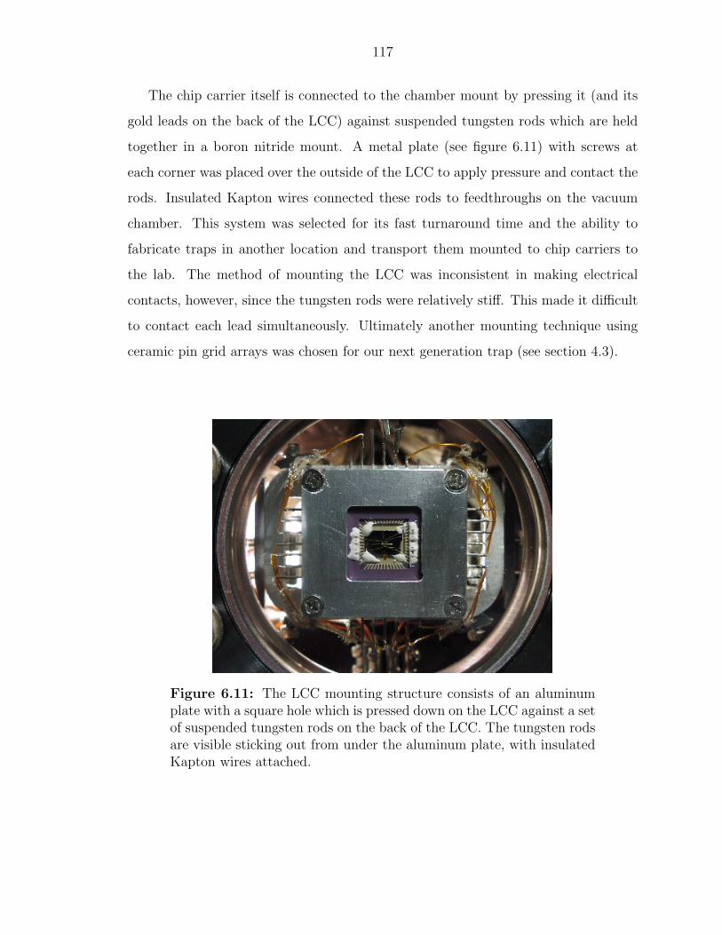
117
The chip carrier itself is connected to the chamber mount by pressing it (and its
gold leads on the back of the LCC) against suspended tungsten rods which are held
together in a boron nitride mount. A metal plate (see figure 6.11) with screws at
each corner was placed over the outside of the LCC to apply pressure and contact the
rods. Insulated Kapton wires connected these rods to feedthroughs on the vacuum
chamber. This system was selected for its fast turnaround time and the ability to
fabricate traps in another location and transport them mounted to chip carriers to
the lab. The method of mounting the LCC was inconsistent in making electrical
contacts, however, since the tungsten rods were relatively stiff. This made it difficult
to contact each lead simultaneously. Ultimately another mounting technique using
ceramic pin grid arrays was chosen for our next generation trap (see section 4.3).
Figure 6.11: The LCC mounting structure consists of an aluminumplate with a square hole which is pressed down on the LCC against a setof suspended tungsten rods on the back of the LCC. The tungsten rodsare visible sticking out from under the aluminum plate, with insulatedKapton wires attached.

118
6.6 Experimental results
Loading ions in the GaAs trap was a formidable task, as the maximum applicable
RF voltage resulted in a trap depth of only a few times room temperature. The
strategy employed was to search through a parameter space of applied DC voltages
(to eliminate bias fields) for a particular RF voltage and frequency value, and if
unsuccessful, repeat for a slightly higher RF voltage and frequency. During these tests
the stability parameter q was held constant at ∼ .7, which is below the maximum
stability value of .92. If we wanted to increase the trap depth Ψ → αΨ(α > 1) and
yet maintain the same q, we had to increase the voltage V → αV and drive frequency
Ω →√
αΩ. Since the power dissipation goes as (V Ω)2, Pdis → α3Pdis. This cubic
increase in power dissipation for only a linear increase in trap depth required us to
be cautious and methodical in increasing the voltage and drive frequency of the trap.
6.6.1 Operating parameters
Eventually we succeeded at loading a single cadmium ion, as seen in the CCD
image capturing the ion’s fluorescence in figure 6.12. A Doppler cooling laser tuned
within one natural linewidth of the 111Cd+ 2S1/2 →2 P3/2 transition near 214.5 nm was
necessary for constant cooling of the ion. It had up to ∼ 1 mW of power focused to a
∼ 15 µm waist. The photoionization laser had about 1 mW of average power focused
to a ∼20 µm waist. With both beams aligned, a single 111Cd+ could be loaded after
a few seconds, at which time the photoionization laser was blocked. Storage lifetimes
in excess of 1 hour were observed provided constant Doppler cooling, with a mean
lifetime of 10 minutes (see figure 6.13). In the histogram a clear hump is seen at about
22 minutes. This is attributed to the pressure decrease immediately after trapping an
ion. Often we had to aggressively fire the oven to trap in a reasonable time period,
and the pressure remained high for the first few minutes after the oven was turned off.
The short lifetime events seen in the graph were likely due to background collisions
as a result of the increased pressure. The local maximum at 22 minutes reveals the

119
average time an ion can be expected to last in the trap before a normal background
collision can be expected (ie not due to the oven). This lifetime, while lower than our
other traps, is consistent with the expected time between elastic collisions [6] with a
room-temperature background gas. In other deeper traps, the ion could potentially
survive a collision or near collision, but in the GaAs trap such a collision was always
fatal. This is also consistent with the fact that we never saw two ions in the same
trap, a common occurrence in other traps we operated.
Figure 6.12: A composite image of a single trapped Cd+ ion alonga view perpendicular to the chip plane after ∼ 1 s of integration time.The ion fluorescess from applied laser radiation directed at a 45 angleto the chip surface and nearly resonant with the Cd+ 2S1/2 −2 P3/2
electronic transition at a wavelength of 214.5 nm. The fluorescence isimaged onto a CCD camera with an f/2.1 objective lens, resulting in anear diffraction limited spot with ∼ 1 µm resolution at the ion. Theprofile of the electrodes is also clearly visible as scattered radiation froma deliberately misaligned laser that strikes the electrodes. The verticalgap between the top and bottom electrodes is s = 60 µm.
We directly measure the frequency of small oscillationg of the trapped ion by

120
Figure 6.13: This histogram shows the lifetime statistics for 32 dif-ferent ions while being continuously Doppler cooled. The events arebinned into time groupings of 0-5 minutes, 5-10 minutes, . . . . The sec-ond peak at the 20-25 minute bin suggests that once an ion has survivedpast the high pressure period caused by the oven being fired, it is mostlikely to last till this 20-25 minute period. Most ions, however, do notsurvive this long due to a collision with a background molecule or Cdatom.

121
applying a weak, variable frequency potential to one of the nearby electrodes and
observe changes in the ion fluorescence owing to the resonant force while it is con-
tinuously laser cooled [36]. For an applied radiofrequency potential amplitude of V0
= 8.0 V at a drive frequency of Ω/2π = 15.9 MHz and a static DV voltage of 1.00
V on the end-cap electrodes and -0.33 V on the center electrodes, we measured the
axial secular frequency to be ωz/2π = 1.0 MHz. The measured transverse secular fre-
quencies were ωx/2π = 3.3 MHz and ωy/2π = 4.3 MHz, indicating a radiofrequency
trap stability factor of q = .62. These measurements are consistent with a three
dimensional numerical simulation of the trapping potential, which further indicates
that one of the transverse principal axes of the trap is rotate ∼ 40 out of the plane
of the chip (this is the x axis).
Additionally, we suppressed micromotion along the direction of the Doppler cool-
ing beam by applying static offset potentials to electrodes that minimize both the
broadengin of the atomic fluorescence spectrum (half-width of ∼ 50 MHz, compared
with the natural half-width of 30 MHz) and the time correlation of the atomic fluo-
rescence with the trap drive frequency (figure 6.14).
6.6.2 Motional heating
Of particular concern for this trap was the anomalous heating rate. We had
evidence that it was relatively high from the observation that without continuous
Doppler cooling the ion would boil out of the trap within τ ∼ .1 s (see figure 6.15).
This lifetime is contingent upon both the heating rate and the trap depth, and due to
the anharmonic nature of the trap at the point where the potential turns around, is
difficult to estimate the heating rate at the bottom of the trap based on the boil-out
time.
To make a quantitative determination of the motional heating rate at the bottom
of the trap we performed stimulated Raman spectroscopy on the hyperfine qubit levels
of the ion. Given the already high temperature of the ion, it was not possible to per-
form the standard sideband thermometry technique discussed in section 2.2.6 because

122
Figure 6.14: This data shows the 100 MHz linewidth achieved in theGaAs trap after compensating voltages were applied to DC electrodes.Multiple data series are shown, with fits to the narrowest two. Thefrequency on the bottom refers to the drive frequency of the 1 GHzdouble pass AOM that is used to lock the laser to the Tellurium ref-erence line. Since this light is double passed and then gets doubled inthe BBO cavity afterwards, the actual frequency should be multipliedby 4. The peak of the resonance occurs at 894 MHz.

123
Figure 6.15: These statistics show the boil out time of an ion which isnot laser cooled. Many more samples could be taken than in figure 6.13because the time duration was shorter and a single ion could providemany data points at short time durations. From the graph it can beseen that the ion has about a 50% chance of surviving for .1 s, whichgives an indication of the heating rate in the trap.
we could not cool to near the ground state using Raman sideband thermometry. By
using the fact that the Raman transition rate is suppressed by the Debye-Waller fac-
tor which is temperature dependent, we could measure this suppression for different
delay times. In figure 6.19 we can see the difference between the Raman transition
rates for data taken .002 ms after the Doppler cooling beams were turned off and
data taken 1 ms after the doppler cooling beam was turned off.
To perform this experiment required a combination of the techniques discussed
in chapter 2, including initialization, detection, and as mentioned driving Raman
carrier transitions. We achieved an initialization fidelity of ∼ 95%, as can be seen
in the dark state counts from figure 6.16. A long Raman carrier transition can be
seen in figure 6.17; the high heating rate increases the temperature for long Raman
transition times, causing a dephasing and loss of coherence visible in the figure. The
probability tends towards the bright state due to detection beam leakage from the
AOM; otherwise it would tend towards a 50% bright state probability. The Raman
frequency scan shown in figure 6.18 gives shows the carrier as well as red and blue

124
sidebands of the Raman transition.
Figure 6.16: This screenshot of the dark state initialization and de-tection shows an experiment being run in which the initializing π beamis applied for 5 µs followed by the detection beam for 200 µs. Whenthe bright state probability is low (∼ 5%), the π beam is unblocked,and when it is bright (∼ 95%), the π beam is blocked.
6.6.3 Motionally sensitive carrier transition
To drive these motionally sensitive stimulated Raman transitions (SRTs) requires
a pair of laser beams detuned ∼ 70 GHz from the 2S1/2 →2 P3/2 transition with an
optical beat note near the 14.53 GHz atomic hyperfine splitting. The two Raman
beams have a 7 angular separation, with the wavevector difference oriented 45 from
the axis of the trap. This nearly copropogating Raman arrangement was chosen to
minimize the axial Lamb-Dicke parameter (η ∼ .018) such that even high thermal
occupation levels would have a measurable carrier transition rate.

125
Figure 6.17: This screenshot shows several Rabi flops on the carriertransition in the GaAs trap. The loss of contrast is due to the decoher-ence as a result of the high heating rate in the trap. It tends towardsthe bright state because of AOM leakage.
Figure 6.18: This Raman frequency scan shows the carrier transitionas well as the red and blue sidebands at ∼ ± 1 MHz.

126
Figure 6.19: The Raman transition probability shown here are depen-dent on the temperature of the ion as quantified by the Debye-Wallerfactor. This is evident from the reduced transition rate seen in an ionwhich is not laser cooled for T = 1 ms, as opposed to the case wherethe Raman transition is measured immediately after (T=0s). Since thetransition is only fitted to 7 µs of Raman data (the black lines), thetime for an experiment is not significant compared to the delay time.
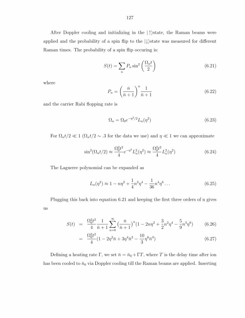
127
After Doppler cooling and initializing in the | ↑〉state, the Raman beams were
applied and the probability of a spin flip to the |↓〉state was measured for different
Raman times. The probability of a spin flip occuring is:
S(t) =∑
n
Pn sin2
(Ωnt
2
)(6.21)
where
Pn =
(n
n + 1
)n1
n + 1(6.22)
and the carrier Rabi flopping rate is
Ωn = Ω0e−η2/2Ln(η2) (6.23)
For Ωnt/2 1 (Ωnt/2 ∼ .3 for the data we use) and η 1 we can approximate
sin2(Ωnt/2) ≈ Ω20t
2
4e−η2
L2n(η2) ≈ Ω2
0t2
4L2
n(η2) (6.24)
The Laguerre polynomial can be expanded as
Ln(η2) ≈ 1− nη2 +1
4n2η4 − 1
36n4η6 . . . (6.25)
Plugging this back into equation 6.21 and keeping the first three orders of n gives
us
S(t) =Ω2
0t2
4
1
n + 1
∞∑n=0
( n
n + 1
)n(1− 2nη2 +
3
2n2η4 − 5
9n3η6) (6.26)
=Ω2
0t2
4(1− 2η2n + 3η4n2 − 10
3η6n3) (6.27)
Defining a heating rate Γ, we set n = n0 +ΓT , where T is the delay time after ion
has been cooled to n0 via Doppler cooling till the Raman beams are applied. Inserting

128
this above gives
S(t)
t2=
Ω20
4[(1− 2η2n0 + 3η4n2
0 −10
3η6n3
0) (6.28)
−2η2ΓT (1− 3
2η2ΓT − 3η2n0 +
5
3η4Γ2T 2 + 5η4n2
0 + 5η4n0ΓT )] (6.29)
= A−BT (6.30)
If we assume that η2n0 1, which is reasonable if the ion is Doppler cooled to
nD (η2nD ∼ .01), then we can take the ratio BA
= 2η2Γ → Γ = B2Aη2 .
We took data at three time delays (see figure 6.20): 0 µs, 500 µs, and 1000 µs.
In the final data analysis we actually had three sets of the graphs seen in the figure,
taking the average of the heating rate values found from a linear fit in each graph.
This is because the data was taken at different times, and in order for the Rabi
frequency to drop out in the ratio BA, the Rabi frequency has to be the same for each
time delay. Since the beam position and power can drift over time, we took data at
T = 0, 500 µs, and 1000 µs, and then repeated, rather than taking multiple data sets
at one time delay.
The initial Raman transition rate is fit to the function f(t) = a + bt2 in Mathe-
matica, and errors are determined assuming a Gaussian distribution about the mean.
This is repeated for the three time delays above, and a line is fit to that data, taking
into account the error for each data point. The intercept and slope of this line are
the coefficients A± σA and B ± σB, giving us a final heating rate of:
Γ =B
A±
√(σB
A)2 + (
B
AσA)2 (6.31)
From the three values we get for Γ, we get a mean value of Γ = −1.2±.4 quanta/µs.
This value only includes statistical errors, not systematic errors. Unavoidable sys-
tematic error in this calculation are the ignored terms in equation 6.28. To make the
problem more clear, we will rewrite B as:

129
Figure 6.20: The suppression of the Raman transition after a givendelay time T is shown in this graph. A line is fit to the data to determinethe slope and intercept, from which the heating rate can be derived.
B = 2η2ΓA
(1−
−η2n0 + 2η4n20 − 3
2η2ΓT + 5η4n0ΓT + 5
3η4Γ2T 2
1− 2η2n0 + 3η4n20
)(6.32)
If we assume that n0 << ΓT for T = 500 µs and 1000 µs, this leads to a correction
in the mean heating rate which will make it lower than the fit would indicate (see
figure 6.21). By factoring that correction in we get a final heating rate for the GaAs
trap of Γ = −1.0± .5 quanta/µs.
We can now compare this value to that predicted from the boil-out time shown
in figure 6.15. As mentioned before, this calculation is complicated by the fact that
the trap becomes anharmonic farther away from the center (this will be discussed in
greater detail in chapter 8), but we can make an upper-bound estimate of the heating
rate at the bottom of the trap based on assuming that it is harmonic up till the trap
depth, so that the heating rate is Γ ≤ Emax
hωxtlifetime≈ 60 quanta/µs. Note that this
is not measuring the same heating rate as measured with the Raman transition rate
experiment above, as that heating rate was along the weak axis, and this measures it
along the transverse axis. It is an upper bound on the heating rate at the bottom of the

130
0.65
0.7
0.75
0.8
0.85
0.9
0.95
1
0 200 400 600 800 1000
Cor
rect
ion
fact
or
Average thermal occupation n
Figure 6.21: The Raman transition rate can be parameterized byA and B, which would ideally be independent of temperature. Thisgraph shows that the coefficient B, as a linear function of A, is notindependent of temperature, and must be accounted for in the finalheating rate estimate of Γ ≈ 1 quanta per µs.
trap because the spectrum of electric field noise as determined in other experiments
[56, 29] has a ∼ 1/f dependence, so that the heating rate should be faster the hotter
the ion is, and therefore we are overestimating Emax (or underestimating tboil) for the
perfectly harmonic case. The fact that this method predicts a factor of 60 greater
heating rate than the Raman transition measurement suggests that the trap is quite
anharmonic far away from the trap minimum. Another possible explanation could
be that the heating mechanism that heats in the direction perpendicular to the trap
surface is stronger than the one that heats along the trap axis; this is unlikely, however,
given that the high aspect ratio of the trap makes the electric field component in this
perpendicular direction small compared to the lateral components.
6.7 Future work on two layer traps
In trying to isolate the source of the anamolously high heating rate in the above
trap, we searched for the mechanical resonance of the cantilevers using an interferom-

131
etry setup that detected the motion of the cantilevers. The cantilevers were driving
with a 1 V oscillating voltage source to attempt to excite this resonance, but no
conclusive resonances were found. To get more heating statistics for another GaAs
trap we plan on fabricating a similar structure out of substrate with 10 µm thick
Al.7Ga.3As layers (thanks to Greg Peake of Sandia National Labs). This will allow us
to apply much more voltage because the electric field in the insulator layer will drop
by a factor of 2.5 and the power dissipated will drop by 2.52 for the same voltage
applied.
In our GaAs traps we observed that the ion would move when a laser was applied
to an electrode, due to the positive charge imbalance in the area that the laser hit.
This is a promising technique for controlling and shuttling ions in a region in which it
is difficult to have separated DC electrodes. While we have been able to demonstrate
15 µm shuttling with this technique, we would like to further explore its affect on
the ion, especially whether power fluctuations of the laser have a large affect on the
heating of the ion. If they do not, this proposal would offer a solution to the speed
limit on shuttling, currently set by low pass filters with a shoulder in the 100’s of
kHz.
We are also looking at fabricating a nearly identical structure out of doped silicon,
using silicon oxide as an insulator. This structure was fabricated by using the process
shown in figure 6.22. Starting with a heavily doped silicon substrate, 2 µm of thermal
oxide were grown on the structure. Then another heavily doped silicon wafer was
annealed on top ofthe oxide layer and mechanically polished down till it is only 5 µm
thick. These two steps are repeated again till the same two layer electrode insulator
structure is achieved as in the GaAs trap.

132
Figure 6.22: A nearly identical structure to that grown with MBE onGaAs can also be fabricated with silicon and silicon oxide. The processstarts (1) with a doped silicon wafer with a thermal oxide layer grownon it. Then (2) another doped silicon wafer is annealed to this firstone, physically attaching the two. After mechanically polishing thissecond wafer down to 5 µm (3), another layer of oxide is grown and theprocess is repeated (4-6), resulting a two layered silicon/silicon oxideheterostructure.

CHAPTER 7
Other microfabricated traps
During my work on the GaAs trap, the Disruptive Technology Office (formerly
ARDA) began to sponsor an effort to have outside foundries design and build ion
traps which could be scaled to larger systems. As part of my research over the last
two years I have been involved in designing the vacuum chamber to host these traps,
discussing system requirements with the foundry researchers, and finally testing the
traps. This chapter will describe their fabrication processes and our results.
7.1 Lucent trap
The first surface trap was demonstrated at NIST [57] in 2006. It was fabricated on
a fused quartz substrate, which was chosen for its low RF loss insulator properties.
Gold electrodes were evaporated and then electroplated on top of the quartz in a
pattern similar to that shown in figure 3.17c. In this trap the RF node is 40 µm
above the surface, and all laser beams come across the surface at an angle to the
weak axis. A promising attribute of this trap is the low heating rate of 5 quanta/ms,
which is small given the ion-electrode distance. The success of this trap along with
the natural advantages of surface traps (discussed in section 3.6) inspired a version
fabricated by a group at Lucent, headed by Dick Slusher.
7.1.1 Fabrication
As seen in figure 7.1, these surface traps are fabricated on a silicon substrate with
133

134
a layer of silicon nitride insulating the substrate from the aluminum/tungsten DC
electrodes. Below the silicon nitride layer is an aluminum ground plane. On top of
the nitride layer are two 10 µm tall rails of silicon oxide which hold the RF electrodes
off the surface of the trap. These are used to decrease the capacitance between the
RF rail and the DC electrodes and allow for higher RF voltage to be applied before
breakdown. On top of these rails is a metal layer of aluminum with a bottom layer
of tungsten which forms the RF electrodes. The capacitance between the RF rail
and one DC electrode is ∼ .1 pF, whereas the capacitance between the DC electrode
and ground is ∼ 30 pF, giving a 300:1 ratio of capacitance which shows that the DC
electrodes are effectively RF grounded. A top view of a trap can be seen in figure 7.2.
The RF rails get closer together as they move from left to right in this figure.
There are four different spacings: 150 µm, 125 µm, 100 µm, and 75 µm. The DC
control electrodes in the region where the RF rails are separated by 150 µm are 300
µm wide; everywhere else they are 200 µmwide, with the exception of an electrode
meant to separate two ions that is 60 µm wide. The RF rails themselves are 20 µm
wide.
7.1.2 Simulations
Because the electrodes on the surface trap are not symmetric about the RF nodal
axis, simulations in CPO were particularly useful for determining static voltages which
would have zero electric field at the node, and therefore minimal micromotion. To
achieve this, the standard simulations are first performed in CPO: 1 volt is applied
to the RF rails to find the ponderomotive potential, and then 1 volt is applied to
each of the other electrodes while the others are grounded. These DC voltages are
linearly added in Mathematica to find an overall DC voltage. After the ponderomotive
potential is calculated (see figures 7.3, 7.4, 7.5), the RF minima is found at a position
x0, y0.
Once this RF minima is found, the DC potential is calculated for the case where
1 volt is applied to each of the outer left electrodes and a volts are applied to the
135
Planar Ion TrapScalable Silicon VLSI
etched SiO2
~ 10Pm
RF Electrodes ~ 1Pm ThickW/Al 20 Pm Wide
p+ doped Si wafer0.018 :cm
~6:
Control ElectrodesW/Al ~ 0.5 Pm Thick
Ground Plane~ 1 Pm Al
Isolation SiN
~0.4 Pm
CRF
CC
CRF/CC > 100
Figure 7.1: This transverse image of the Lucent surface trap (imagecourtesy of Dick Slusher) shows a cross section of the silicon substrateand electrodes comprising the trap. The RF rails run the length of thetrap, with the DC electrodes arranged next to each other like railroadties.

136
Revised Linear Trap
Al RF electrode surface
20 Pm
ControlelectrodesRF
electrode
Figure 7.2: This overhead view of the Lucent surface trap (imagecourtesy of Dick Slusher) shows the DC control electrodes above andbelow the RF rails. The RF rails come closer to each other while run-ning from left to right, so that heating measurements can be performedin traps with varying ion height. There is one central DC electrodewhich is connected at the right end (out of view).
Figure 7.3

137
Figure 7.4
Figure 7.5

138
middle left one (figure 7.6, where l = 1, r = c = 0). The voltage a is varied until the
electric field in the x direction is 0 at the RF node, i.e. Ex(x0, y0) = 0. Now a voltage
c is applied to all electrodes, including the RF rails, until the vertical electric field is
zero at the RF node, i.e. Ey(x0, y0) = 0. Because the same voltage c is applied on all
of the electrodes, there will be no Ex component to c, and so now there is no offset
electric field at the node. The same analysis can be done for the right electrodes.
By applying r volts to the outside right electrodes and ar volts to the middle right
electrode, Ex(x0, y0) remains 0. However now Ey(x0, y0) 6= 0; to compensate, we have
to add an additional rc volts to all electrodes. To make this more general, we now
scale the left outside electrodes to have l volts on them. Once a and c are determined,
r and l can be varied in any desireable way (as long as the trap is not destabilized)
and Ex(x0, y0) = Ey(x0, y0) = 0. The final applied voltages are shown in figure 7.6.
Figure 7.6: To minimize the static electric field at the trap node, theconstants a and c must be determined from CPO simulations. Oncethese are determined, any voltage r and l can be chosen and the electricfield at the RF node will be zero.

139
An example of a DC potential in which the electric field is zero at the RF node can
be seen in figure 7.7. The voltages applied to each side are not equal (l 6= r) in order
to tilt the principal axes of the trap - this can be seen in the contour lines leaning
off to one side. Without tilting DC voltages applied, the principal axes are naturally
perpendicular and parallel to the plane of the trap. Since the cooling laser comes
across the surface of the trap, it is perpendicular to the vertical principal axis, and
therefore does not cool the ion’s motion in that direction. Therefore the principal axes
have to be tilted by applying different voltages to the left and right electrodes. When
the ponderomotive potential is combined with the DC potential, the total potential
that the ion sees (minus the micromotion driven terms) is shown in the contour plot in
figure 7.8. The tilt of the principal axes can be seen in figure 7.9. The difficult aspect
of choosing l and r in order to achieve sufficient tilt is that it significantly weakens
the nearly vertical axis. Once l and r are chosen such that the axes are tilted and
the trap is sufficiently deep, the secular frequency in both the axial direction and
both transverse directions is determined, as well as the trap depths. The potential
is plotted along these axes and a quadratic fit to the trap minima is calculated to
determine the secular frequency.
7.1.3 Operating parameters and results
Of the three traps that we received, we were only able to trap successfully in the
first one. This one did not have an aluminum ground plane as shown in figure 7.1,
and subsequently had a lower Q than other tested traps (Qloaded ∼ 100). In traps with
this ground plane the loaded Q was closer to 150. We were able to trap in the region
with the 150 µm separated RF electrodes, with the height of the trap 75 µm above the
surface. The applied voltages which successully trapped can be seen in figure 7.11.
They generated a principal axis rotation of 12 , a trap depth of .5 eV, and transverse
secular frequencies of 5.9 MHz and 5.7 MHz. Up till now we had only applied a
maximum of 370 VRF to the rails, with up to 10 VDC to the control electrodes. Even
still we were noticing some of the DC electrodes were shorting to the ground plane

140
Figure 7.7: This contour plot of the total DC potential applied to thesurface trap shows how the principal axes are tilted from perpendicularand parallel to the surface of the trap.
Figure 7.8: The total surface trap potential, including the pseudopo-tential and the static potential.

141
Figure 7.9: The orange lines designate the principal axes of the surfacetrap, as determined by finding the eigenvectors of the Hessian matrixat the trap minima. Typical values for this tilt are between 5 and 15.
Figure 7.10: The axial potential of the trap is plotted here. Therange extends beyond the edges of the middle electrode (which is .3mm long), which explains the anharmonic nature of the trap. Thesecular frequency in this direction is determined by fitting a harmonicpotential to the bottom of the trap.
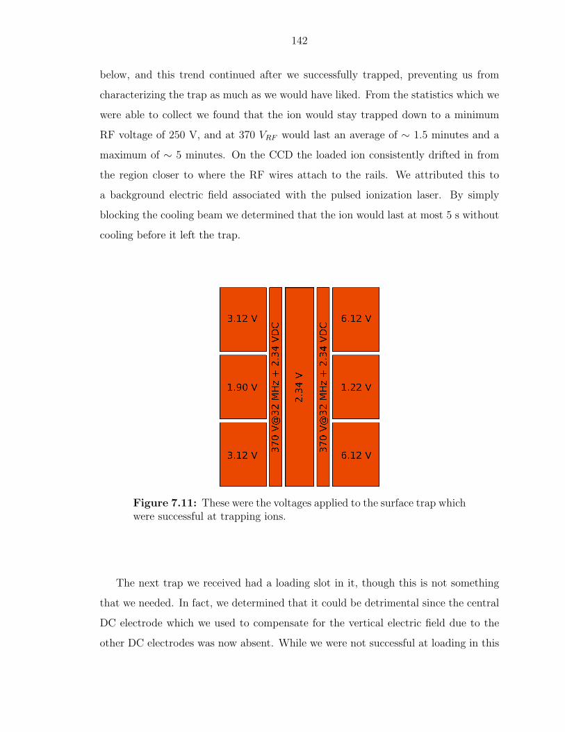
142
below, and this trend continued after we successfully trapped, preventing us from
characterizing the trap as much as we would have liked. From the statistics which we
were able to collect we found that the ion would stay trapped down to a minimum
RF voltage of 250 V, and at 370 VRF would last an average of ∼ 1.5 minutes and a
maximum of ∼ 5 minutes. On the CCD the loaded ion consistently drifted in from
the region closer to where the RF wires attach to the rails. We attributed this to
a background electric field associated with the pulsed ionization laser. By simply
blocking the cooling beam we determined that the ion would last at most 5 s without
cooling before it left the trap.
Figure 7.11: These were the voltages applied to the surface trap whichwere successful at trapping ions.
The next trap we received had a loading slot in it, though this is not something
that we needed. In fact, we determined that it could be detrimental since the central
DC electrode which we used to compensate for the vertical electric field due to the
other DC electrodes was now absent. While we were not successful at loading in this

143
trap, the group at NIST has successfully used it. From communications with them
[58], they witnessed similar lifetimes, problems with DC electrode breakdown, and
the ion drifting in from along the RF rail after the photoionization laser is turned
off. The last Lucent trap that we received did not have a backside loading slot and
did have an aluminum grounding plane. Electrically this trap seemed fine from our
in situ measurements of its Q (∼ 150) and the RF and DC electrode capacitances.
Nonetheless, we were unsuccessful at trapping in this version, and are waiting to try
it again in the future.
Assuming the problems encountered with the first few iterations of the Lucent
trap can be solved through improved fabrication and operation methods, the upsides
to the surface trap are great. For one, surface traps can be combined with on board
optics - such as the MEMS mechanical mirrors shown in figure 7.12.
One final area of interest for surface traps is the issue of making a junction. Many
trapping geometries suffer from the presence of an RF hump right before the junction
region. This feature requires the ion to be shoved over the hump into the junction re-
gion where it can be pushed out again. In this process a great deal of motional energy
is imparted to the ion (see chapter 5). To minimize this, researchers at NIST [40]
have been working with analytic solutions to the trapping potential and have deter-
mined surface trap electrode shapes which minimize the residual pseudopotential that
comprises the RF hump. In figure 7.13 they show that differently shaped electrodes
in the junction region can reduce the RF hump maxima by two orders of magnitude.
Interestingly, they note that the curvature of the RF hump does not decrease so dras-
tically, which may mean that significant motional heating is still inevitable through
this region.
7.2 Sandia trap
Another type of trap that we tested was fabricated at Sandia National Labs
through an effort led by Matt Blain. This trap used a single layer geometry like
that shown in figure 3.15a. The RF electrodes as seen in figure 7.14 are made of

144
Figure 7.12: This conceptual design of a surface (image courtesy ofDick Slusher) trap shows a possible solution to the problem of havingmany lasers coming across the surface of the trap which could interferewith ions in other traps. By fabricating movable mirrors in conjuctionwith the trap, the ions could be illuminated by lasers which reflectoff of mirrors positioned and activated depending on the operation tobe run. This schematic also shows CMOS circuitry underlying thetrap array. By having a library of necessary routines which wouldbe necessary for shuttling or storage, for instance, the electrical controlsignals, which would otherwise require one wire going out of the vacuumchamber for each electrode, could be run through addressable CMOSlogic. Given the large number of separate traps necessary for a viablequantum computer, this aspect will have to be part of any seriousproposal.

145
Figure 7.13: The three junctions shown here (image courtesy of JanusWesenberg) show three different surface electrode geometries in thejunction region. From the graph, it is seen that the RF hump potentialΦP can be supressed by two orders of magnitude simply by shaping theelectrodes. A result of the electrode shaping and subsequent RF humpminimization is that the height of the ion above the trap changes inthe junction region, although this is not a particular concern. The insetshows that the curvature of ΦP is not so drastically supressed, and thismay have more of an implication for the motional heating of the ion asit passes through a junction.

146
deposited tungsten wires which are held under tension by anchors to each far end of
the trap. They use a unique set of circular links which can flex under the tension, so
that when the underlying layer is released they do snap under the stress.
Figure 7.14: The Sandia trap consists of one layer of tungsten elec-trodes. The RF wires are not solid, but rather consist of linked circleswhich can flex under the tension provided by the anchors. This tensionis a result of the release step which leaves them suspended over emptyspace. The DC electrodes are supported on the edge of the hole.
While the NIST and Innsbruck groups were able to demonstrate the Sandia trap,
we were not able to get it to work. This trap has extremely low capacitance, but as
a diagnostic we were able to check that the electrodes were connected as expected by
illuminating them with the photoionization laser and detecting the resulting current.
The loaded Q of the trap was 70, as expected. Having recently switched lasers for
the trap development project, we have recently confirmed that part of the setup by
trapping in the needle trap, and plan on testing the Sandia trap again.

147
7.3 Polysilicon MEMS Exchange trap
The polysilicon trap came out of a proposal for MEMS Exchange, which is a
consortium of fabrication facilities used by researchers to fabricate non-production
size fabrication jobs. Our proposal to fabricate a two layer ion trapping structure out
of polysilicon was started by Bill Noonan is currently being led by Michael Pedersen.
One advantage of using polysilicon is a somewhat higher conductivity compared to
GaAs - our structure has a sheet resistance of 7.5 Ω/square for electrodes that are
only .75 µm thick. Additionally, the fact that the structure can be fabricated on
a silicon substrate allows the possibility in the distant future of integrating CMOS
components with it. In the near term, it has the advantage of the backside etch being
a relatively simple and accurate KOH etch. Since the polysilicon can be deposited
after various processing steps (as opposed to the GaAs MBE requirement), it is much
more flexible as far as having vertical structure. For instance, the bridges which NIST
uses to make a junction in a two layer trap would be possible in a polysilicon trap.
The ability to use polysilicon glass as a temporary spacer before it is removed via
wet etching allows air gaps to be used instead of a material insulator between the
polysilicon layers. This allows for larger breakdown voltages and lower capacitances
between the polysilicon layers. Though the air gap (2 µm) is half as thick as in the
GaAs trap, the lack of material means that the capacitance is 5 times smaller, so
the power dissipated is 25 times smaller than in the GaAs trap, given roughly equal
electrode resistances.
Figure 7.16 shows the structure up till the bond pad metallization step. Figure
7.17 shows the final structure after the backside etch. As of the time of the writing of
this thesis, MEMS Exchange was having a dificult time removing the silicon nitride
from the bottom of the bottom layer cantilevers without damaging them. We have
decided that it should not be a serious concern and hope to have the first polysilicon
traps in the summer of 2007.

148
Figure 7.15: This figure shows the important steps in the polysiliconfabrication process (images courtesy of Michael Pedersen). The firststeps are to grow thermal oxide and nitride on the wafer as insula-tion and future masking layers. Then the bottom phosphorous dopedpolysilicon layer is grown and etched. Polysilicon glass is grown ontop of this to space out the second polysilicon layer. At this point thebackside nitride and oxide are removed. Then the top layer polysiliconelectrodes are defined through a reactive ion etch, and HF is used toexpose the electrodes so that chromium and gold can be deposited toform bond pads. After etching the excess metal, a KOH defines thebackside hole, followed by a buffered HF etch and an isotropic wet etchto remove all polysilicon glass, and the cantilevers are released after asupercritical dry step.
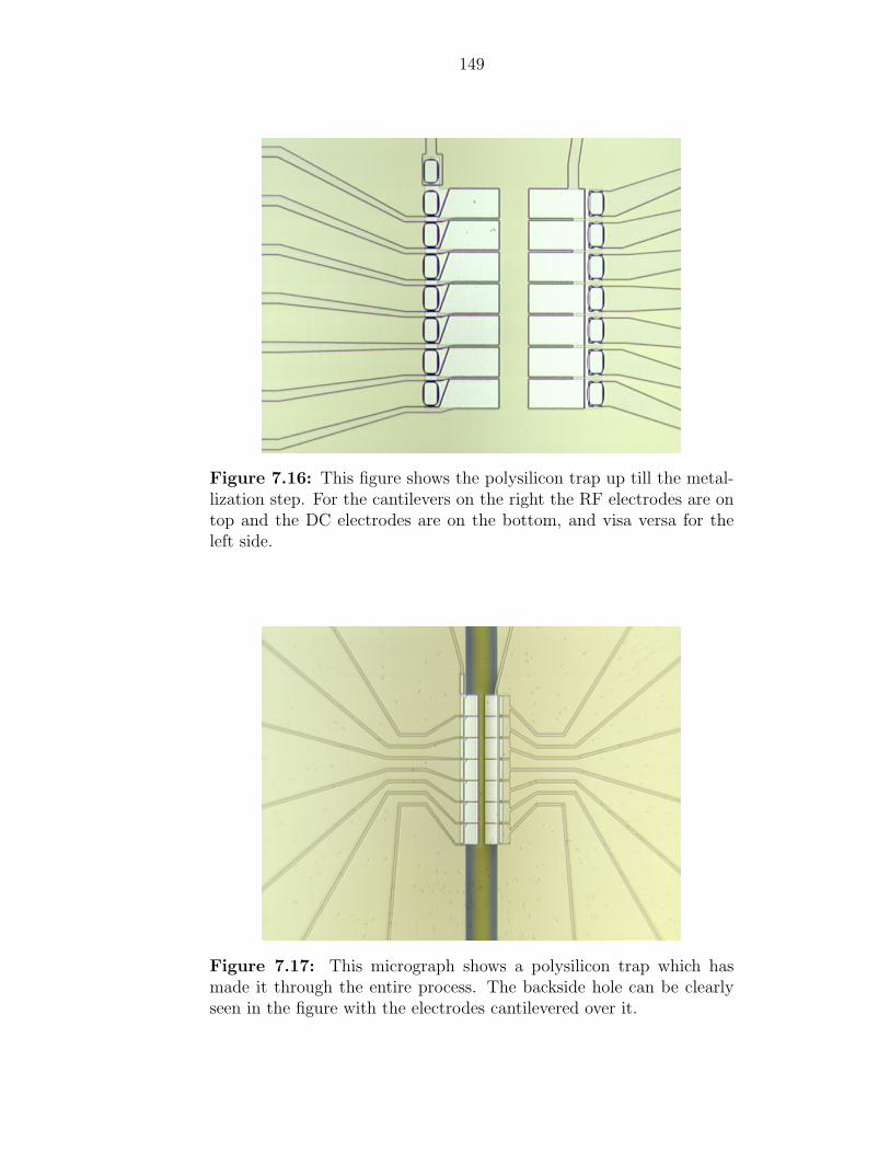
149
Figure 7.16: This figure shows the polysilicon trap up till the metal-lization step. For the cantilevers on the right the RF electrodes are ontop and the DC electrodes are on the bottom, and visa versa for theleft side.
Figure 7.17: This micrograph shows a polysilicon trap which hasmade it through the entire process. The backside hole can be clearlyseen in the figure with the electrodes cantilevered over it.

CHAPTER 8
Sources of motional heating
Voltage fluctuations on surrounding electrodes couple to the motional energy of
the ion, in essence heating it. The two primary contributers are thermal (Johnson)
noise and patch potential noise, aptly named because it describes voltage fluctuations
on a particular region, or patch. When the electrodes are at room temperature, it is
orders of magnitude more influential than thermal noise. The subject of heating is
particularly important for the microfabricated traps because the spectral density of
electric field noise is observed to scale as ∼ 1/z40 with the ion-electrode distance z0,
and the typically low potential depths of a microtrap combined with a high heating
rate make continuous laser cooling necessary to retain the ion. In addition to ion
traps, a related type of noise is observed in other systems, including solid state QC
systems [59] and precision measurements of gravity involving proximate masses [60].
In setting out to design an ion trap capable of characterizing the patches in situ,
we first had to determine the relevant parameters to vary. From figure 8.1 we see a
plot of many different ion traps used in various groups to trap a variety of species
[56]. From this plot we can see that regardless of the material used in the trap (this
graph shows traps made out of molybdenum, gold coated alumina, and GaAs), the
spectral density of electric field noise was similar in each of them, to within about
an order of magnitude. Also obvious is the strong dependence on the ion electrode
distance. And finally, based on the gray area showing the level of Johnson noise, we
can tell that patch potential noise was the dominant effect in each trap. We therefore
set out to make a trap with movable electrodes such that the distance z0 could be
150
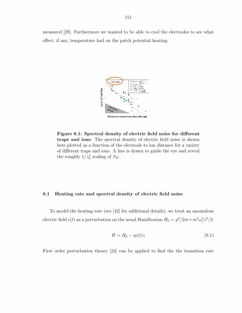
151
measured [29]. Furthermore we wanted to be able to cool the electrodes to see what
effect, if any, temperature had on the patch potential heating.
Figure 8.1: Spectral density of electric field noise for differenttraps and ions: The spectral density of electric field noise is shownhere plotted as a function of the electrode to ion distance for a varietyof different traps and ions. A line is drawn to guide the eye and revealthe roughly 1/z4
0 scaling of SE.
8.1 Heating rate and spectral density of electric field noise
To model the heating rate (see [42] for additional details), we treat an anomalous
electric field ε(t) as a perturbation on the usual Hamiltonian H0 = p2/2m+m2ω2zz
2/2:
H = H0 − qε(t)z (8.1)
First order perturbation theory [24] can be applied to find the the transition rate
152
from the |0〉 state to the |1〉 state:
Γ0→1 =1
h2
∫ ∞
−∞dτeiωzτ 〈ε(t)ε(t + τ)|〉〈0|qz|1〉|2 (8.2)
=q2
4mhωz
SE(ωz) (8.3)
This is the ˙n heating rate that we measure when the ion is first cooled to the
ground state and then probed after a delay time with the sideband thermometry
technique discussed in chapter 2. We have to add a term corresponding to heating of
the micromotion oscillation, so that equation 8.2 becomes:
Γ0→1 = ˙n =q2
4mhωz
(SE(ωz) +ω2
z
2Ω2SE(Ω± ωz)) (8.4)
Note that the micromotion term is at the drive frequency modulated by the secular
frequency, Ω±ωz, as seen from equation 3.11. This additional heating term is reduced
by a factor of ω2z
2Ω2 , and so can be ignored for most traps.
8.2 Thermal (Johnson) noise
The incoherent sum of all sources of noise due to thermally fluctuating charges in
a conductor [61] is called Johnson noise. The voltage noise from a thermal source is:
SV (ω) = 4kBTR(ω) (8.5)
and it is treated as being correlated over the entire electrode. The sum of all these
thermal noise sources Ri (given that there are two needles) is [29]:
SV (ω) =∑
i
8kBTiRi(ω)
1 + Ri(ω)2C2i ω
2(8.6)
The various Ri sources can be seen in figure 8.2. The dominant contributer is the
needle itself, primarily because it is unfiltered. The RF choke RF and the resonator
resistance Rres, although both larger, are filtered and so do not contribute signifi-

153
cantly.
To find the effect of the voltage noise on the ion, we compare it to a parallel plate
capacitor separated by 2z0. In this case the electric field noise at the ion would be:
SE(ω) =SV (ω)
(2z0)2(8.7)
In the case of the needle we parametrize its efficiency compared to the capacitor with
ε:
SE(ω) = SV (ω)
(ε
2z0
)2
(8.8)
From numerical simulations in Maxwell we were able to determine that ε ≈ .7 for
the dimensions of the second needle. Given this, we estimate the total Johnson noise
contribution to the heating rate at 300 K to be ˙n ∼ (200/z0)2(ωz/2π)−1, for z0 in µm
and ωz/2π in MHz. When the temperature is lowered from 300 K to 150 K we expect
the Johnson noise heating rate contribution to fall by a factor of 6; a factor of 2 due
to the thermal noise dependence and a factor of 3 due to the resistance in tungsten
dropping.
The affect of patch potential noise requires more intensive simulations, as the
patch potentials are not considered to be correlated over the size of the needle. For
this reason simulations have to be done in which a patch of size α located at position
k has 1 volt applied, and the electric field in z is measured, at an ion-needle distance
z0. The electric field then is Ez = Vnξk,α,z0 . If we plug this formula for Ez into
equation 8.2 and sum over all positions k for a single patch size and needle spacing,
we can bring the constant sum out front and get:
SE(ω) = 2(∑
k
(ξk,α,z0)2)SV (ω) (8.9)
That sum Ξα(z0) =∑
k(ξk,α,z0)2 could then be plotted versus z0 for different values
of α and compared with actual data to find α.
8.3 Trap construction

154
The chosen moveable electrode geometry uses two needles attached to linear posi-
tioners (see figure 8.2). This type of trap is similar to the hyperbolic traps discussed in
chapter 3, with the difference that the radius of the ring electrode is taken to inifinity.
From numerical simulations performed in Maxwell 3D, it was found that the needle
tips had to be have a sufficiently low curvature in order to maintain a reasonably high
trapping strength, as parametrized by the η variable in equation 8.10:
ωz =
√eV0η
mz20
+ (eV0η√2Ωz2
0
)2 (8.10)
Also, it was discovered after testing the first needle trap that cylindrical electrodes
recessed from the needle tips were necessary to shield the ion from stray electrice
fields that built up on the insulator. Although the first trap iteration (consisting
of just needles and no cylindrical grounds) was able to trap, the micromotion of
the ion changed over time periods of 10 minutes as a result of repeated firing of the
photoionization laser. It is suspected that when the laser hits the boron nitride needle
mount (directly or after reflecting off the viewport) it becomes charged up, and that
as that charge changes the bias electric fields at the ion changes, which increases the
micromotion.
Adding the grounding sleeves also had the added benefit of increasing the efficiency
of the trap. In the first needle trap there was no sleeve, and the radius of curvature
of the needle tip was ∼ 8 µm. With these dimensions, η ranged from .08 to .12 as z0
ranged from 25 µm to 75 µm. In the second needle, which had a grounded sleeve 2.3
mm recessed from the end of the needle and a tip with a 3 µm radius of curvature, η
ranged from .16 to .18 as z0 ranged from 25 µm to 250 µm. In each case the needle
electrodes were made out of tungsten rods which were mechanically polished (with a
dremel tool and fine grain sand paper) and chemically polished (with phosphoric and
HF acid) to a point with a 4 half angle. Typical operating values for this trap are
U0 = 0 and V0 = 600 at Ω/2π = 29 MHz and z0 = 136 µm, ωz/2π = 2.77 MHz.
8.4 Heating results

155
Figure 8.2: Needle schematic: This schematic diagram of the nee-dle trap shows the vacuum chamber, liquid nitrogen cooled cold fingers,and needle and sleeve electrodes in part a. The inset shows a compositeimage of the actual needles illuminated on the CCD camera with an ionin the middle. In part b the circuit diagram for the needle structure isshown.
First the heating rate ˙n was measured as a function of the trap frequency (figure
8.3) using sideband thermometry. In this case the trap distance was fixed at z0 = 103
µm while keeping V0 = 600 V and changing U0 to change the trap frequency ωz. The
graph shows the data from this experiment (the last point uses V0 = 700 V). The fit
to this data reveals ˙n ∼ ω−1.8±.2, or SE(ω) ∼ ω−.8±.2 obeys a 1/f noise scaling law.
Secondly, the heating rate was measured as a function of ion-electrode spacing z0.
From figure 8.4, the 300 K data follows a relatively straight line (corresponding to
a power law in this log log plot). The data was taken at a trap frequency of ωz/2π
= 2.07 MHz, where both the static and RF voltages were changed as z0 changed to
maintain the same trap frequency. The line is fit to ˙n ∼ z−3.5±.10 . At 150 K, the
second and third data points were taken with ωz/2π = 2.07 MHz, while the first
point was taken at ωz/2π = 4.9 MHz and scaled according to the fit in figure 8.3.
Based on previous experiments we know that increased RF voltage does not increase
the heating rate, provided the secular frequency and distances are the same. The
gray region shows the heating rate from thermal noise expected for this trap; for
both of the temperature showns here it is well over an order of magnitude lower than
that measured. Additionally, the observed noise does not follow the expected 1/z20

156
Figure 8.3: Heating rate in the needle trap as a function oftrap frequency: In this experiment the RF potential and trap dis-tance were held constant, only varying U0 to change ωz.
relationship with heating rate and distance.
8.5 Future work - molybdenum trap
We are currently in the process of testing a needle trap nearly identical to the
aforementioned needle, but with needles made of molybdenum rather than tungsten.
Molybdenum was chosen because the work function of its oxide is nearly identical to
the work function of the metal. It is thought that electrons hopping from the metal
to the oxide could be related to the source of patch potential noise, and by using a
metal where there is no potential difference between these transitions, perhaps the
anomalous heating rate will be suppressed. Additionally, there is historical evidence
that molybdenum is an ideal material as a ring and fork molybdenum trap was tested
with a heating rate so low it could not be measured with sideband thermometry. That
heating rate eventually rose over the course of the experiment due to contamination
from the ovens being fired.
An additional feature of the molybdenum trap is the heaters on each needle to
provide finer temperature control. While liquid nitrogen will still be used to cool the
electrodes, the heaters (which consist of tungsten wire wrapped around a ceramic

157
Figure 8.4: Heating rate in the needle trap as a function oftrap distance: In this experiment the trap frequency was held con-stant while the needles were moved apart with the linear positioner,varying U0 and V0 to maintain a constant ωz.
core and covered by a ceramic tube) will be able to regulate more finely (there are
thermocouples on each needle mount as well) the temperature of the needle. We hope
this data will give further insight into the nature of patch potentials.
CHAPTER 9
Conclusion
In conclusion, the experiments presented here, namely constructing microfabri-
cated traps, shuttling ions in junction regions, and characterizing motional heating
due to patch potentials on the trap electrodes, are meant to demonstrate the efficacy
of constructing a trapped ion quantum computer. My focus has been on the scalability
requirement, leaving discussions on the progress made in the other equally important
DiVincenzo criteria (section 1.4) to other texts and research groups [30, 62]. Over the
last few years research in extending the number of entangled qubits [63], improving
gate fidelities, and increasing coherence times has achieved impressive results and
had a postivitive effect in driving interest in the work presented here. While the time
frame is uncertain, hopefully it is apparent to the reader that the field of trapped ion
quantum computing holds a promising future.
158

BIBLIOGRAPHY
159

BIBLIOGRAPHY
[1] W Paul. Electromagnetic traps for charged and neutral particles. Rev. Mod.Phys., 62:531–540, 1990.
[2] H G Dehmelt. Radiofrequency spectroscopy of stored ions i: Storage. Adv. Atom.Mol. Phys., 3:53–72, 1967.
[3] F Diedrich, J C Bergquist, W M Itano, and D J Wineland. Laser cooling to thezero-point energy of motion. Phys. Rev. Lett., 62(14):403–406, October 1989.
[4] D L Moehring, B B Blinov, D W Gidley, R N Kohn Jr., M J Madsen, T BSanderson, R S Vallery, and C Monroe. Precision lifetime measurement of asingle trapped ion with ultrafast laser pulses. Phys. Rev. A, 73:023413, 2006.
[5] S Diddams, T Udem, J C Bergquist, E A Curtis, R E Drullinger, L Hollberg,W M Itano, W D Lee, C W Oates, K R Vogel, and D J Wineland. An opticalclock based on a single trapped 199hg+ ion. Science, 293:825–828, 2001.
[6] D J Wineland, C Monroe, W M Itano, D Leibfried, B E King, and D M Meekhof.Experimental issues in coherent quantum-state manipulation of trapped atomicions. J. Res. Nat. Inst. Stand. Tech., 103:259–328, May 1998.
[7] D P Divincenzo. The physical implementation of quantum computation.Fortschritte der Physik, 48:771–783, 2000.
[8] M J Bass and C M Christensen. The future of the microprocessor business. IEEESpectrum, 39(4):34–39, 2002.
[9] R P Feynman. Simulating physics with computers. Int. J. Th. Phys.,21(6/7):467–488, 1981.
[10] D. Deutsch. Quantum-theory, the church-turing principle and the universal quan-tum computer. Proceedings of the Royal Society of London Series A - Mathe-matical, Physical, and Engineering Sciences, 400(1818):97 – 117, 1985.
[11] P W Shor. Algorithms for quantum computation: Discrete logarithms and fac-toring. In Proceedings of the 35th Annual Symposium on the Foundations ofComputer Science, page 124, New York, 1994. IEEE Computer Society, IEEEComputer Society Press.
[12] M Nielsen and I Chuang. Quantum Computation and Quantum Information.Cambridge University Press, 2000.
[13] C Pomerance. A tale of two sieves. Notices of the AMS, pages 1473–1485, 1996.
160

161
[14] 2005.
[15] A Steane. Error correcting codes in quantum theory. Phys. Rev. Lett., 77(5):793–796, July 1996.
[16] S Aaronson. Np-complete problems and physical reality. quant-ph/0502072,2005.
[17] D P DiVincenzo. Quantum computation. Science, 270(1):255–261, October 1995.
[18] P O Schmidt, T Rosenband, C Langer, W M Itano, J C Bergquist, and D JWineland. Spectroscopy using quantum logic. Science, 309:749–752, 2005.
[19] C Monroe, D M Meekhof, B E King, W M Itano, and D J Wineland. Demonstra-tion of a fundamental quantum logic gate. Phys. Rev. Lett., 75(25):4714–4717,December 1995.
[20] F schmidt Kaler, H Haffner, M Riebe, S Gulde, G Lancaster, T Deuschle,C Becher, C Roos, J Eschner, and R Blatt. Realization of the Cirac-Zollercontrolled-NOT quantum gate. Nature, 422:408–411, 2003.
[21] K Mølmer and A Sørensen. Multiparticle entanglement of hot trapped ions.Phys. Rev. Lett., 82:1835–1838, 1999.
[22] J J Garcia-Ripoll, P Zoller, and J I Cirac. Speed optimized two-qubit gates withlaser coherent control techniques for ion trap quantum computing. Phys. Rev.Lett., 91:157901, 2003.
[23] M Acton, K A Brickman, P C Haljan, P J Lee, L Deslauriers, and C Monroe.Near-perfect simultaneous measurement of a qubit register. Quantum Informa-tion and Computation, 6:465, 2006.
[24] Richard Liboff. Introductory Quantum Mechanics, 3rd Ed. Addison-Wesley, NewYork, 1998.
[25] R Ozeri, C Langer, J D Jost, B DeMarco, A Ben-Kish, B R Blakestad, J Britton,J Chiaverini, W M Itano, D B Hume, D Leibfried, T Rosenband, P O Schmidt,and D J Wineland. Hyperfine coherence in the presence of spontaneous photonscattering. Phys. Rev. Lett., 95:030403, 2005.
[26] D J Wineland, R E Drullinger, and F L Walls. Radiation-pressure cooling ofbound resonant absorbers. Phys. Rev. Lett., 40:1639–1642, 1978.
[27] D J Wineland and W M Itano. Laser cooling of atoms. Phys. Rev. A, 20(4):1521–1540, October 1979.
[28] H J Metcalf and P van der Straten. Laser Cooling and Trapping. Springer, NewYork, 1999.

162
[29] L Deslauriers, S Olmschenk, D Stick, W K Hensinger, J Sterk, and C Monroe.Scaling and suppression of anomalous quantum decoherence in ion traps. Phys.Rev. Lett., 97:103007, 2006.
[30] D Leibfried, R Blatt, C Monroe, and D Wineland. Quantum dynamics of singletrapped ions. Rev. Mod. Phys., 75:281, 2003.
[31] P K Ghosh. Ion Traps. Clarendon Press, Oxford, 1995.
[32] G. M. Murphy. Ordinary Differential Equations and their Solutions. D. VanNostrand Company, Inc., Princeton, NJ, 1960.
[33] N. W. McLachlan. Theory and Application of Mathieu Functions. Dover Publi-cations, Inc., New York, NY, 1964.
[34] H G Dehmelt. Advances in Atomic and Molecular Physics, volume 3. AcademicPress, Inc., New York, 1967.
[35] B Blinov, L Deslauriers, P Lee, M Madsen, R Miller, and C Monroe. Sympatheticcooling of trapped cd+ isotopes. Phys. Rev. A, 65:040304, 2002.
[36] S R Jefferts, C Monroe, E Bell, and D J Wineland. Coaxial-resonator driven rf(paul) trap for strong confinement. Phys. Rev. A, 51(4):3112–3116, April 1995.
[37] M Madsen, W Hensinger, D Stick, J Rabchuk, and C Monroe. Planer ion trapgeometry for microfabrication. Appl. Phys. B, 78:639, 2004.
[38] S R Valluri, D J Jeffery, and R M Corless. Some applications of the lambert wfunction to physics. Can. J. Phys, 78:823, 2000.
[39] J Chiaverini, R B Blakestad, J Britton, J D Jost, C Langer, D Leibfried, R Ozeri,and D J Wineland. Surface-electrode architecture for ion-trap quantum informa-tion processing. Quantum Information and Computation, 5(6):419–439, 2005.
[40] J Wesenberg and R Reichle. private communication, 2006.
[41] W W Macalpine. Coaxial resonators with helical inner conductor. Proceedingsof the IRE, 1959.
[42] Q A Turchette, D Kilepinski, B E King, D Leibfried, D M Meekhof, C J Myatt,M A Rowe, C A Sackett, C S Wood, W M Itano, C Monroe, and D J Wineland.Heating of trapped ions from the quantum ground state. Phys. Rev. A, 61:063418,June 2000.
[43] L Deslauriers, M Acton, B Blinov, K Brickman, P Haljan, W Hensinger, D Hucul,S Katnik, R Kohn, P Lee, M Madsen, P Maunz, S Olmschenk, D Moehring,D Stick, J Sterk, M Yeo, K Younge, and C Monroe. Efficient photoionizationloading of trapped ions with ultrafast pulses. Phys. Rev. A, 74(6):063421, 2006.

163
[44] A Yariv and P Yeh. Optical Waves in Crystals. John Wiley & Sons, New York,1984.
[45] P J Lee, B B Blinov, K Brickman, L Deslauriers, M J Madsen, R Miller, D LMoehring, D Stick, and C Monroe. Atomic qubit manipulations with an electro-optic modulator. Optics Lett., 28:1852, 2003.
[46] K A Brickman, P C Haljan, P J Lee, M Acton, L Deslauriers, and C. Monroe.Implementation of grover’s quantum search algorithm in a scalable system. Phys.Rev. A, 72(050306(R)), 2005.
[47] W Hensinger, S Olmschenk, D Stick, D Hucul, M Yeo, M Acton, L Deslauriers,C Monroe, and J Rabchuk. T-junction ion trap array for two-dimensional ionshuttling, storage, and manipulation. Applied Physics Letters, 88(3), 2006.
[48] M A Rowe, A Ben-Kish, B DeMarco, D Leibfried, V Meyer, J Beall, J Britton,J Hughes, W M Itano, B Jelenkovic, C Langer, T Rosenband, and D J Wineland.Transport of quantum states and separation of ions in a dual rf ion trap. QuantumInformation and Computation, 2(4):257–271, 2002.
[49] D Hucul, M Yeo, W K Hensinger, J Rabchuk, S Olmschenk, and C Monroe.On the transport of atomic ions in linear and multidimensional ion trap arrays.arxiv, quant-ph/0702175, 2007.
[50] J P Cleveland, S Manne, D Bocek, and P K Hansma. A nondestructive methodfor determining the spring constant of cantilevers for scanning force microscopy.Rev. Sci. Instr., 64:403–405, 1993.
[51] R G Beck, M A Eriksson, R M Westervelt, K D Maranowski, and A C Gossard.Measuring the mechanical resonance of a gaas/algaas cantilever using a strain-sensing field-effect transistor. Semicond. Sci. Tech., 13:A83–A85, 1998.
[52] et al D E Aspnes. Gaas lower conduction band minima: Ordering and properties.Phys. Rev. B, 14(12):5331–5343, 1976.
[53] M Mangalaraj, M Radhakrishnan, and C Balasubramanian. Electrical conduc-tion and breakdown properties of silicon nitride films. Journal of Materials 17,pages 1474–1478, 1982.
[54] D Rutledge. The electronics of radio. Cambridge University Press, Cambridge,UK, 1999.
[55] Ralph Williams, editor. Modern GaAs Processing Methods. Artech House,Boston, MA, 1990.
[56] L Deslauriers, P C Haljan, P J Lee, K-A Brickman, B B Blinov, M J Madsen,and C Monroe. Zero-point cooling and low heating of trapped cd ions. Phys.Rev. A, 70:043408, 2004.
164
[57] S Seidelin, J Chiaverini, R Reichle, J J Bollinger, D Leibfriend, J Britton, J H We-senberg, R B Blakestad, R J Epstein, D B Hume, W M Itano, J D Jost, C Langer,R Ozeri, N Shiga, and D J Wineland. Microfabricated surface-electrode ion trapfor scalable quantum information processing. Phys. Rev. Lett., 96:253003, 2006.
[58] D Leibfried. private communication, 2006.
[59] J M Martinis, S Nam, J Aumentado, K M Lang, and C Urbina. Decoherence ofa superconducting qubit due to bias noise. Phys. Rev. B, 67:094510, 2003.
[60] C W Stubbs, E G Adelberger, F J Raab, J H Gundlach, B R Heckel, K DMcMurry, H E Swanson, and R Watanabe. Search for an intermediate-rangeinteraction. Phys. Rev. Lett., 58(11):1070–1073, 1987.
[61] J Johnson. Thermal agitation of electricity in conductors. Phys. Rev., 32:97,1928.
[62] D Leibfried, B DeMarco, V Meyer, D Lucas, M Barrett, J Britton, W M Itano,B Jelenkovic, C Langer, T Rosenband, and D J Wineland. Experimental demon-stration of a robust, high-fidelity geometric two ion-qubit phase gate. Nature,422:412–415, 2003.
[63] H Haffner et al. Scalable multiparticle entanglement of trapped ions. Nature,438:643–646, 2005.