Embed Size (px)
Citation preview
Materials Letters 63 (2009) 933–936
Contents lists available at ScienceDirect
Materials Letters
j ourna l homepage: www.e lsev ie r.com/ locate /mat le t
Fabrication of a porous polyimide membrane using a silicon nanowire arrayas a template
Woong Kim ⁎, Myung-Ki LeeDepartment of Materials Science and Engineering, Korea University, Seoul 136-713, South Korea
⁎ Corresponding author. Tel.: +82 2 3290 3266; fax: +E-mail address: [email protected] (W. Kim).
0167-577X/$ – see front matter © 2009 Elsevier B.V. Aldoi:10.1016/j.matlet.2009.01.060
a b s t r a c t
a r t i c l e i n f oArticle history:
We demonstrate that a po Received 10 October 2008Accepted 17 January 2009Available online 26 January 2009Keywords:NanomaterialsPolymersPorosityMembranesNanowiresPolyimide
rous polyimide membrane can be fabricated by curing liquid polyimide on avertically oriented silicon nanowire array and selectively etching away the nanowire-array-template usingxenon difluoride (XeF2). Pore size and density using the described technique are controllable. The former isdependent on nanowire diameter and the duration of etching, whereas pore density is determined by siliconnanowire density. We believe that the described porous membrane fabrication method can be applied tovarious polymer and nanowire systems.
© 2009 Elsevier B.V. All rights reserved.
1. Introduction
Porous polymer membranes have many applications in biotech-nology and electronics for the separation and/or filtration of gases,biomolecules, and environmentally hazardous materials, and as in-sulating materials with low dielectric constants [1–4]. It has also beenrecently demonstrated that porous polymer membranes can be usedas templates to synthesize silicon nanowires electrochemically [5].Among the many polymers available, polyimide (PI) has been widelyused in academia and industrially due to its high thermal stability,good chemical resistance, and excellent mechanical properties [6].Porous polyimide membranes have been prepared via the phaseinversion of cast films [7], by irradiationwith energetic heavy ions andsubsequent oxidization [8], and by the decomposition of thermallylabile domains in phase-separated block copolymers [4]. In this letter,we describe the preparation of a porous polyimide membrane using avertically oriented silicon nanowire (SiNW) array as a template. Sincethe diameters and densities of silicon nanowires can be controlled,polyimide membranes with predetermined pore densities anddiameters can be readily produced using the described technique.
2. Experimental procedures
Silicon nanowires were synthesized on silicon (111) substrates bychemical vapor deposition (CVD) as described elsewhere [9]. Briefly,gold (Au) nanoparticles were deposited on silicon substrates ascatalytic seeds. SiCl4 (the silicon source) was then introduced into a
82 2 928 3584.
l rights reserved.
CVD reactor containing a silicon substrate at 850 °C using H2 (10%) inAr as a carrier gas. Silicon nanowires grew vertically from substrates.
Polyimide solution (PI-2556) was purchased from HDMicrosystems.A drop of this solution was applied onto silicon substrates withnanowires. The solution was cured at 200 °C for 30 min in a nitrogenstream, which resulted in a solid polyimide membrane over theembedded nanowires. The membrane was then slightly etched with O2
plasma (20 min at 100 W in a 50 sccm O2 stream) to expose the siliconnanowire tips. Au nanoparticles at the tips of the nanowires were thenetched using potassium iodide and iodine (KI/I2) solution, and thesubstratewas thoroughly rinsedwith deionized (DI) water. To selectivelyetch the silicon nanowires and leave the polyimide membrane intact,XeF2 etching was carried out over 50–200 cycles of exposure to 4 Torr ofXeF2 and 2 Torr of N2 for 60 s. Polyimide membranes were eitherdetached from silicon substrates after this stage or were detached bydipping substrates in buffered hydrofluoric acid (BHF) solution. Forscanning electronmicroscopy (SEM) characterizations, about 5 nm of Auwas sputtered onto the polyimide membranes produced.
3. Results and discussion
The procedure used to fabricate the porous polyimide membranesis summarized in Fig. 1. As a first step, silicon nanowires wereepitaxially grown on Si (111) substrates by CVD. Since nanowires growpreferentially in theb111Ndirection under the conditions used, theywere oriented vertically to the substrate. An SEM image of an angledview of the vertically aligned silicon nanowires is shown in Fig. 1a.Since nanowires grow via a vapor liquid solid (VLS) mechanism, goldnanoparticles (AuNPs) are retained at the tips of the nanowires; theseappeared as bright dots in SEM images (Fig. 1a).
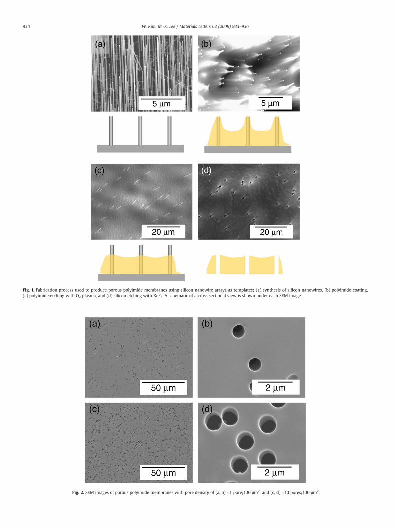
Fig. 1. Fabrication process used to produce porous polyimide membranes using silicon nanowire arrays as templates; (a) synthesis of silicon nanowires, (b) polyimide coating,(c) polyimide etching with O2 plasma, and (d) silicon etching with XeF2. A schematic of a cross sectional view is shown under each SEM image.
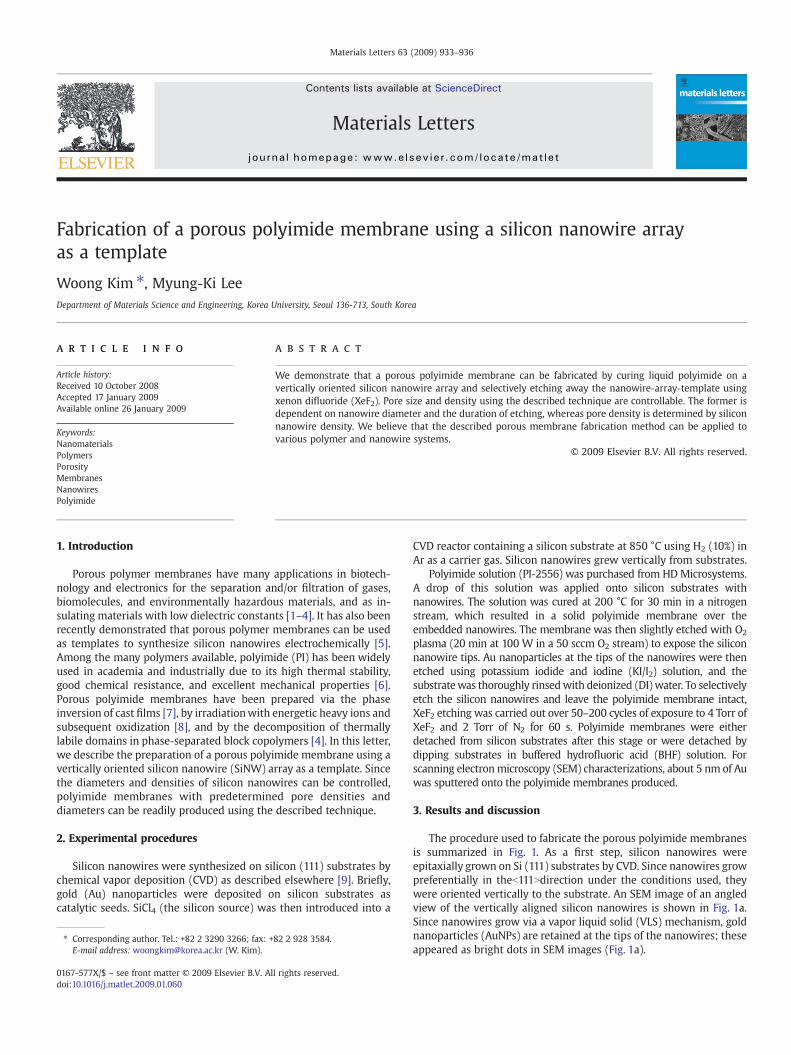
Fig. 2. SEM images of porous polyimide membranes with pore density of (a, b) ~1 pore/100 μm2, and (c, d) ~10 pores/100 μm2.
934 W. Kim, M.-K. Lee / Materials Letters 63 (2009) 933–936
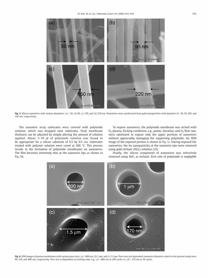
Fig. 3. Silicon nanowires with various diameters; (a) ~50, (b) 90, (c) 150, and (d) 220 nm. Nanowires were synthesized from gold nanoparticles with diameter of ~30, 50, 100, and150 nm, respectively.
935W. Kim, M.-K. Lee / Materials Letters 63 (2009) 933–936
The nanowire array substrates were covered with polyimidesolution, which was dropped onto substrates. Final membranethickness can be adjusted by simply altering the amount of solutionapplied. About 5–10 μl of polyimide solution was found tobe appropriate for a silicon substrate of 0.5 by 0.5 cm. Substratestreated with polymer solution were cured at 200 °C. This processresults in the formation of polyimide membranes on nanowires.The film becomes extremely thin at the nanowire tips as shown inFig. 2b.
Fig. 4. SEM images of porousmembranes with various pore sizes; (a) ~800 nm, (b) 1 μm, and90, 150, and 400 nm, respectively. Pore size is dependent on etching time, e.g., (a) ~800 nm
To expose nanowires, the polyimide membrane was etched withO2 plasma. Etching conditions, e.g., power, duration, and O2 flow rate,were optimized to expose only the upper portions of nanowireswithout appreciably damaging the supporting polyimide. An SEMimage of the exposed portion is shown in Fig. 1c. Having exposed thenanowires, the Au nanoparticles at the nanowire tips were removedusing gold etchant (KI/I2) solution [10].
Finally, the silicon component of nanowires was selectivelyremoved using XeF2 as etchant. Etch rate of polyimide is negligible
(c) 1.5 μm. Pore sizes are dependent nanowire diameter, which in the present study wereat 200 cycles vs. (d) ~170 nm at 50 cycles.
936 W. Kim, M.-K. Lee / Materials Letters 63 (2009) 933–936
compared to that of silicon [10]. Fig. 4b shows the top surface of a pore-containing polyimide membrane after this selective etching process.
Asmentionedearlier,membraneporedensity iswholly dependentonnanowire density, which is in turn determined by gold nanoparticledensity. Moreover, there is usually a near one to one relation betweennanowire and gold nanoparticle numbers [11]. Fig. 2 shows twomembranes with different pore densities. A membrane with a poredensity of ~1/100 μm2 is shown in SEM images with differentmagnifications (Fig. 2a and b), and a membrane with density of ~10pores/100 μm2 is shown in Fig. 2c and d.
The pore size can also be controlled, as it is dependent on two factorsonly; namely, template-nanowire diameter and the duration of XeF2etching. On the other hand, wire diameter is determined by goldnanoparticle size and is slightly larger than the AuNP seeds. Fig. 3 showsnanowires with various diameters of ~50, 90, 150 and 220 nm syn-thesized from Au nanoparticles with diameter of ~30, 50 100 and150 nm, respectively. Fig. 4 a, b, and c show polyimide membranesfabricated using silicon nanowires with diameter of ~90, 150, and400 nm, respectively. After exposure to XeF2 for 200 cycles, theresulting pore diameter were ~800 nm,1 μmand 1.5 μm, respectively.Etching time also affected pore size. For example, 90 nm siliconnanowires resulted in pore diameters of ~170 nm when membraneswere exposed to XeF2 for 50 cycles (Fig. 4d), while the final porediameter was ~800 nm when 200 cycles were used (Fig. 4a).Interestingly, when etching timewas reduced, the original hexagonalcross sections of the nanowires were transferred to the pores (Fig.4d). Further optimization of the described process is expected toincrease the ranges of the pore diameters and densities formed.
4. Conclusions
Our studies indicate that silicon nanowires can be used assacrificial templates for the fabrication of porous polyimide mem-
branes. Moreover, since the densities and diameters of silicon nano-wires can be easily adjusted, membranes can be fabricated with pre-determined pore densities and sizes. In the present study, membraneswere successfully fabricated with pore diameters ranging from170 nm to 1.5 μm and densities ranging from 0.1 to 1 pore/10 μm2.Furthermore, the novel fabrication technique described can be appliedto the fabrication of porous membranes from different polymers andtemplate nanowires comprising different materials.
Acknowledgement
This work was supported in part by the Korea Science andEngineering Foundation through the Pioneer Converging TechnologyProgram (No. M10711160001-08M1116-00110).
References
[1] Pandey P, Chauhan RS. Prog Polym Sci 2001;26:853–93.[2] Ulbricht M, Yang H. Chem Mater 2005;17:2622–31.[3] Mendelsohn JD, Barrett CJ, Chan VV, Pal AJ, Mayes AM, Rubner MF. Langmuir
2000;16:5017–23.[4] Hedrick JL, Miller RD, Hawker CJ, Carter KR, Volksen W, Yoon DY, et al. Adv Mater
1998;10:1049–53.[5] J. Mallet, M. Molinari, F. Martineau, F. Delavoie, P. Fricoteaux, M. Troyon, Nano Lett
2008;8:3468–74.[6] Wilson AM. Thin Solid Films 1981;83:145–63.[7] Echigo Y, Iwaya Y, Saito M, Tomioka I. Macromolecules 1995;28:6684–6.[8] Trautmann C, Bruchle W, Spohr R, Vetter J, Angert N. Nucl Instrum Meth Phys Res
Sect B-Beam Interact Mater Atoms 1996;111:70–4.[9] Hochbaum AI, Fan R, He RR, Yang PD. Nano Lett 2005;5:457–60.[10] Williams KR, Gupta K, Wasilik M. J Microelectromech Syst 2003;12:761–78.[11] Wang DW, Tu R, Zhang L, Dai HJ. Angew Chem Int Ed 2005;44:2925–9.