Embed Size (px)
Citation preview

FABRICATION OF ARRAY WAVEGUIDE GRATINGS (AWGS) FOR MULTIPLEXERS/DEMULTIPLEXERS
(MUX/DEMUX) APPLICATION
PUA CHANG HONG
UNIVERSITY OF MALAYA 2009

FABRICATION OF ARRAY WAVEGUIDE GRATINGS (AWGS) FOR MULTIPLEXERS/DEMULTIPLEXERS
(MUX/DEMUX) APPLICATION
By
PUA CHANG HONG Department of Physics
Faculty of Science University of Malaya
Dissertation Presented For The Degree of Master of Science
UNIVERSITY OF MALAYA 2009
ii
UNIVERSITY OF MALAYA
ORIGINAL LITERARY WORK DECLARATION
Name of Candidate : Pua Chang Hong (IC No. : 821025-14-5491)
Registration/ Matric No : SGR060042
Name of Degree : Degree of Master of Science
Title of Project Paper/ Research Report/ Dissertation/ Thesis (“this work”):
Fabrication of Array Waveguide Gratings (AWGs) for
Multiplexers/Demultiplexers (MUX/DeMUX) Application
Field of Study: I do solemnly and sincerely declare that:
(1) I am the sole author/ writer of this work; (2) This work is original; (3) Any use of any work in which copyright exists was done by way of fair dealing
and for permitted purposes and any excerpt or extract from, or reference to or reproduction of any copyright work has been disclosed expressly and sufficiently and the title of this work and its authorship have been acknowledged in this work;
(4) I do not have any actual knowledge nor I do ought reasonably to know that the making of this work constitute an infringement of any copyright work;
(5) I hereby assign all and every rights in the copyright to this work to the University of Malaya (“UM”), who henceforth shall be owner of the copyright in this work and that any reproduction or use in any form or by any means whatsoever is prohibited without the written consent of UM having been first had and obtained;
(6) I am fully aware that if in the course of making this work I have infringed any copyright whether intentionally or otherwise, I may be subject to legal action or any other action as may be determined by UM.
Candidate’s Signature Date: Subscribed and solemnly declared before, Witness’s Signature Date: Name : Prof. Dr. Harith Bin Ahmad Designation : Professor

iii
ABSTRACT
In this dissertation, the fabrication process of Arrayed Waveguide Gratings
(AWGs) for Passive Optical Network (PON) implementation is presented. The study is
important to the fabrication of AWGs as the fabrication tools are unique and need to be
optimized. The study is also focuses on the metal masking process for the fabrication of
a quality AWGs patterning process.
Throughout this project, optimization has been carried out for direct-current (DC)
planar magnetron sputtering of Cr, photolithography, and wet etching of Cr. The
optimizations for the Cr metal mask are masking thickness, critical dimension (CD),
side wall angle (SWA), and surface roughness. After the optimization process, we
succeed to increase the patterning yield from 40% up to 100%. The critical dimension
was also being reduced to the range of 0.4 – 0.8μm for 7μm width and 350nm thick Cr-
pattern. The SWA of the photoresist (PR) was improved from 35° to 19°. Due to the
wet etching properties, the surface roughness of the Cr pattern did not seem to be
improved in this project.

iv
ABSTRAK
Dalam disertasi ini, proses fabrikasi “Arrayed Waveguide Gratings” (AWGs)
untuk implementasi dalam rangkaian optik pasif telah dikaji. Kajian ini adalah penting
untuk mengoptimisasikan setiap mesin fabrikasi yang unik supaya dapat menghasilkan
AWGs yang berkualiti. Kajian ini tertumpu pada penghasilan topeng logam yang
berkualiti dalam proses fabrikasi bagi penghasilan corak AWGs.
Sepanjang disertasi ini, kajian dan optimisasi telah dilakukan dalam proses
kromium “DC magnetron sputtering”, fotolitografi, dan pembuangan kromium secara
kimia. Optimisasi ini bertujuan untuk memperbaiki empat parameter utama dalam
penghasilan topeng logam kromium iaitu, ketebalan topeng, dimensi kritikal, sudut
dinding, dan kekasaran permukaan. Selepas kajian dan proses optimisasi, kami berjaya
meningkatkan pengeluaran corak dari 40% sehingga 100%. Bagi dimensi kritikal pula,
telah dikurangkan di antara 0.4 – 0.8μm bagi corak kromium pada kelebaran 7μm dan
ketinggian 350nm. Sudut dinding untuk photo resin telah ditingkatkan dari 35° ke 19°.
Tetapi, kekasaran permukaan dilihat tidak dapat diperbaiki didalam disertasi ini
disebabkan oleh sifat pembuangan kromium secara kimia.

v
ACKNOWLEDGEMENT
I would like to thanks my supervisor, Professor Harith bin Ahmad, for his ideas,
guidance, patience, and all the opportunities he gave. Thanks also to both of my co-
supervisors Associate Professor Sulaiman Wadi Harun and Dr. Fiasal Rafiq Mahamd
Adikan for their guidance, support, and encouraging.
Thousand thanks to my helpful colleagues especially Mr. Chong Wu Yi who
gave all the guidance and kind enough to share his experience and knowledge
throughout my dissertation, Mr. Nizam Tamchek who is not worked under planar
waveguide project but still willing to spend times for giving technical supports and
advices when necessary. Thanks also to other colleagues like Mr. Chuah Koon Seah, Mr.
Alvin Law Wen Pin, Mr. Zamani, Mr. Tan Chin Chong, Mr. Sua Yong Meng, Mr. Lim
Weng Hong, Ms. Yap Yen, Ms. Kow Siew Ting and other that I do not mention for all
the cheers and joys that we share in the laboratory.
I also feel grateful to my family for supporting me to further study and being
understanding. Finally, my gratitude goes to my sponsor – Ministry of Science,
Technology, and Innovation (MOSTI), government of Malaysia for giving me full
financial support, and also University of Malaya that offer me a great place to complete
my thesis.
vi
LIST OF PUBLICATION
1) Pua, C.H., Sulaiman, W.H., Chong, W.Y., Kanesh, J.K., & Harith, A. (2007).
Dynamic Dispersing Technique for PR Coating Process in Planar Lightwave Circuit
Fabrication. Microwave and Optical Technology Letters, 49 (8), 1993-1995.
LIST OF CONFERENCE
1) Pua, C.H., Chong, W.Y., Sulaiman, W.H., & Harith, A. (2007). Influence of Time
and Current on Chromium Thin Film Sputter Deposition by Direct Current (DC)
Planar Magnetron Sputtering System. 3RD Mathematics and Physical Sciences
Graduate Congress (3RD MPSGC) 2007, University of Malaya, Malaysia. 12th to 14th
Dec 2007.
2) Pua, C.H., Chong, W.Y., Sulaiman, W.H., & Harith, A. (2007). Dependence of Cr
Etching Rate on Cr Deposition Thickness by Direct Current (DC) Planar Magnetron
Sputtering System. National Physics Conference (PERFIK) 2007. Kuala
Terengganu, Malaysia. 26-28 Dec 2007.

vii
CONTENTS
PAGE
FRONT PAGE i
DECLARATION ii
ABSTRACT iii
ABSTRAK iv
ACKNOWLEDGEMENT v
LIST OF PUBLICATION vi
CONTENTS vii
LIST OF FIGURES xi
LIST OF TABLES xiv
LIST OF SYMBOLS AND ABBREVIATIONS xv
CHAPTER 1
INTRODUCTION
1.1 WHAT IS A PLANAR LIGHTWAVE CIRCUIT (PLC)? 1
1.1.1 EVOLUTION OF PLC 1
1.1.2 ADVANTAGES OF PLC 3
1.2 WHAT IS ARRAYED WAVEGUIDE GRATINGS (AWGS)? 5
1.2.1 EVOLUTION AND APPLICATION OF AWGS 5
1.2.2 ADVANTAGES OF AWGS IN WDM NETWORK 6
1.3 FABRICATION OF AWGS 6
1.4 MOTIVATION AND OBJECTIVES 8
REFERENCES 9
CHAPTER 2
ARRAYED WAVEGUIDE GRATINGS (AWGS)
2.1 THEORY OF OPTICAL WAVEGUIDE 12
2.1.1 TOTAL INTERNAL REFLECTION (TIR) 12
2.1.2 PRINCIPLE OF OPTICAL WAVEGUIDE 15
2.1.3 OPTICAL WAVEGUIDE ATTENUATION 17

viii
2.2 THEORY OF ARRAYED WAVEGUIDE GRATINGS (AWGs) 18
2.2.1 ATHERMAL AWGs 20
2.2.2 ATHERMAL AWG IN UNIVERSITY OF MALAYA 22
2.2.3 ISSUES AFFECTING THE PERFORMANCE OF AWG 23
REFERENCES 25
CHAPTER 3
FABRICATION OF ARRAYED WAVEGUIDE GRATINGS
3.1 FABRICATION PROCESSES 28
3.2 GLASS FABRICATION 29
3.3 METAL MASKING 31
3.4 GLASS ETCHING 32
3.5 SUMMARY 33
REFERENCES 34
CHAPTER 4
DC MAGNETRON SPUTTER DEPOSITION
4.1 BACKGROUND 35
4.2 THEORY OF SPUTTERING 36
4.2.1 SPUTTERING AND SPUTTER DEPOSITION PROCESSES 36
4.2.2 DC MAGNETRON SPUTTER DEPOSITION 38
4.3 DC MAGNETRON SPUTTERING SYSTEM AND PROCESS
METHODOLOGY IN PHOTONIC RESEARCH CENTER (PRC) 41
4.3.1 WAFER LOADING AND UNLOADING IN LOAD-LOCK
SYSTEM 41
4.3.2 PRC DC PLANAR MAGNETRON SPUTTERING SYSTEM 42
4.3.3 CHROMIUM SPUTTER DEPOSITION PROCESS
METHODOLOGY 45
4.3.4 PUMP PURGE CYCLES AFTER DEPOSITION 47
4.4 EXPERIMENTAL RESULTS AND DISCUSSIONS 47
4.4.1 STUDY OF DEPOSITION TIME 48
4.4.2 DC CURRENT EFFECT ON CHROMIUM DEPOSITION 51
4.4.3 PROCESS PRESSURE EFFECT ON CHROMIUM
DEPOSITION 56

ix
4.5 SUMMARY 59
REFERENCES 60
CHAPTER 5
PHOTOLITHOGRAPHY
5.1 BACKGROUND 62
5.2 THEORY 63
5.2.1 PHOTORESIST (PR) 63
5.2.2 PHOTOLITHOGRAPHY EXPOSURE METHOD 65
5.3 PHOTOLITHOGRAPHY PROCESS METHODOLOGY 68
5.3.1 PR COATING 69
5.3.2 PREBAKE 70
5.3.3 MASK ALIGNER 70
5.3.4 DEVELOPMENT 71
5.3.5 POSTBAKE 71
5.4 EXPERIMENTAL RESULTS AND DISCUSSIONS 72
5.4.1 PHOTORESIST (PR) COATING 72
5.4.2 PREBAKE 76
5.4.3 UV EXPOSE 79
5.4.4 POSTBAKE 85
5.5 SUMMARY 87
REFERENCES 88
CHAPTER 6
WET ETCHING
6.1 INTRODUCTION 89
6.2 OVERVIEW 89
6.3 CR WET ETCHING PROCESS METHODOLOWY 91
6.4 EXPERIMENTAL RESULTS AND DISCUSSIONS 92
6.5 SUMMARY 99
REFERENCES 100

x
CHAPTER 7
CONCLUSIONS & FUTURE WORK
7.1 CONCLUSIONS 101
7.2 FUTURE WORK 104
APPENDIX A 106
APPENDIX B 111

xi
LIST OF FIGURES Page
Chapter 1 Introduction 1.1: 1st Generation Optical Fibre Communication–Point to Point Single
Wavelength System 2 1.2: 4th Generation Optical Fibre Communication–DWDM on point to point
Network System 3 Chapter 2 Arrayed Waveguide Gratings (AWGs) 2.1: Light refraction from one material to another material with different
refractive index where nr > ni 13 2.2: Light refraction on the surface with nr < ni, and θr = 90° 14 2.3: Total Internal Reflection (TIR) where θ1 = θ2 15 2.4: Light ray travel in fiber with different angle, (a) blue colour ray with
incident angle θ1 < θc; (b) black colour ray with incident angle, θc; (c) green ray with incident angle θo > θc 16
2.5: Structure of AWG 18 2.6: Divergent of multiplexed wavelength to arrayed waveguides in first FPZ 19 2.7: Optical ray path of different wavelength at second FPZ 19 2.8: An athermal AWGs packaging design 21 2.9: Athermal AWGs photomask in University of Malaya 22 Chapter 3 Fabrication of Arrayed Waveguide Gratings (AWGs) 3.1: Process flow for the AWGs fabrication 29 3.2: Process flow Metal masking 31 Chapter 4 DC Magnetron Sputter Deposition 4.1: Elastic collision between two hard spheres 36 4.2: Collision of two particles 37 4.3: Schematic of a physical sputtering process 38 4.4: Various types of magnetron cathode 39 4.5: Magnetic field configuration for a circular planar magnetron cathode 40 4.6: DC magnetron sputtering system chamber 42 4.7: Grow discharge at target surface 46 4.8: Cr thickness for different sputtering time 48 4.9: Increment of Cr grains height according to thin film thickness 49 4.10: AFM images of Cr thin film for a) (70±5) nm and b) (330±5) nm
thickness 50 4.11: Etching time for different Cr thickness 51 4.12: The voltage and current as a function of total current drawn by DC glow
discharge 52 4.13: Cr film thickness with DC power supply current, Idc 53 4.14: Cr thickness for different deposition times for different Idc 54 4.15: Cr deposition rate on different DC current supply, Idc 55 4.16: Cr etching rate for different Cr thickness coated with different current 55 4.17: DC power supply for different process pressure 57 4.18: Cr film thickness with different pressure deposition 58 4.19: Etching time difference between the wafer center and edge 59

xii
Chapter 5 Photolithography 5.1: Schematic diagram showing the effect of using positive or negative PR
on silica glass fabrication 63 5.2: Chemical reaction of negative PR under UV radiation to form
crosslinked polymer matrix 64 5.3: Reaction of PAC prior to the exposure of the UV light 65 5.4: Various UV exposure methods used in photolithography process 66 5.5: PR thickness (μm) versus spin coating speed (rpm) for SDT, 1st DDT
and 2nd DDT 73 5.6: Illustration of PR thickness non-uniformity with various PR dispensing
techniques 74 5.7: Thickness variation of PR applied using the 1st DDT approach 75 5.8: PR thickness dependence on various prebake temperatures 76 5.9: PR residual that fail to remove from wafer after PR removal process 77 5.10: PR thickness for prebaking temperature of 60oC, 80oC, and 100oC, for
various prebake duration 78 5.11: Change of PR thickness with various prebaking duration 78 5.12:PR pattern obtained with (a) soft contact, (b) hard contact, and (c) and (d)
for vacuum contact 80 5.13: Error analysis scale on AWG photomask, (a) for CD error measurement
while (b) for resolution limit measurement 80 5.14: Resolution measurements of samples under (a) 0.2MPa and (b) 0.16MPa
contact pressure 81 5.15: Cross-section of PR pattern produced under (a) 0.2MPa and (b) 0.16MPa
contact pressure 82 5.16: Fringe pattern when the photomask is in contact with the PR coated
wafer 82 5.17: PR pattern with different exposure dosage. (a) 1860 mJ/cm2, (b) 1890
mJ/cm2, (c) 1920 mJ/cm2, and (d) 2100 mJ/cm2 84 5.18: Different exposure dosages for varying PR thickness 84 5.19: Resulting PR thickness for different postbake period 85 5.20: Etched Cr patterns with and without postbake condition of 120°C for 2
minutes and without postbake 86 5.21: Cross-section of PR pattern before and after postbake 86 Chapter 6 Wet Etching 6.1: Schematics of undercutting caused by the isotropic nature of wet etching 90 6.2: Cr wet etching time for different Cr deposition periods 92 6.3: Difference in etching time between the edge and center of a wafer in
various chromium deposition times 93 6.4: CD error for Cr pattern after static wet etching 94 6.5: Etching time needed for flipping and static wet etching over various Cr
deposition duration 95 6.6: The significant reduction of EC period for flipping etching as compared
to static etching 95 6.7: CD error for different Cr deposition times 96 6.8: Cr etching time by using static and ultrasonic etching method 97 6.9: CD error for Cr pattern with ultrasonic etching 97 6.10: Cr etching rate at different temperatures 98

xiii
Appendix A Theory and Design of Arrayed Waveguide Gratings (AWGs) A.1: Illustrative diagram of an N x N AWG 106 A.2: Geometry of the FPZ 108 A.3: Focusing of beam in two different wavelengths 109

xiv
LIST OF TABLES Page
Chapter 1 Introduction 1.1: Expansion of Leading Edge Transmission System Achieved with AWGs 6 Chapter 2 Arrayed Waveguide Gratings (AWGs) 2.1: Configuration of athermal AWGs 21 Chapter 3 Fabrication of Arrayed Waveguide Gratings (AWGs) 3.1: Hydrolysis and oxidation reaction of metal chloride materials 30 3.2: Important parameters in different processes 33 Chapter 5 Photolithography 5.1: PR usage in SDT, 1st DDT and 2nd DDT 75 Chapter 6 Wet Etching 6.1: Summary of different Cr wet etching techniques for 6 minutes Cr
deposition period 99

xv
LIST OF SYMBOLS AND ABBREVIATIONS AFM Atomic Force Microscopy Ar Argon Ar+ Argon ion AWGs Arrayed Waveguide Gratings B Boron B2O3 Boric Oxide BCl3 Boron Trichloride CD Critical Dimension CF4 Tetrafluoromethane/ Carbon Tetrafluoride CF3
+ Fluorocarbon ion III Co. Company CO2 Carbon Dioxide Cr Chromium Cr(NO3)3 Chromium (III) Nitrate CVD Chemical Vapour Deposition DC Direct Current DDT Dynamic Dispensing Technique DeMux De-multiplexing DI De-Ionized DOF Depth of Focus DWDM Dense Wavelength Division Multiplexing e Electron EC Edge to centre F Fluorine FBG Fibre Bragg Grating FHD Flame Hydrolysis Deposition FPZ Free Propagation Zone FSR Free Spectral Range g Gas Ge Germanium GeCl4 Germanium Tetrachloride GeO2 Germanium Dioxide H2O Water HCl Hydrogen Chloride HClO4 Perchloric Acid He Helium HF Hydrofluoric Acid IC Integrated Circuit ICP Inductive Couple Plasma InP Indium Phosphide ISEE Ion-Induced Secondary Electron Emmision ITU International Telecommunication Unit K Potassium Kr Krypton LiNbO3 Lithium Niobate Ltd. Limited MFC Mass Flow Controller Mux Multiplexing MZ Mach-Zehnder

xvi
N2 Nitrogen gas NA Numerical Aperture (NH4)2Ce(NO3)6 Ceric Ammonium Nitrate O2 Oxygen OC Over-Clad OPF Optical Path Function P Phosphorus P2O3 Diphosphorus Trioxide PAC Photoactive Compound PECVD Plasma Enhanced Chemical Vapour Deposition PHASARs Phased-Arrayed Gratings PIC Photonic Integrated Circuit PLC Planar Lightwave Circuit POCl3 Phosphorus Oxide Trichloride PON Passive Optical Network PR Photoresist RI Refractive Index RIE Reactive Ion Etching s Solid sccm Standard Cubic Centimeters per Minute SDT Static Dispensing Technique SGD Sol-Gel Deposition Si Silicon SiCl4 Silicon Tetrachloride SiF4 Tetrafluorosilane SiO2 Silica SoI Silica-on-Insulator SoS Silica-on-Silicon SWA Side Wall Angle TE Transverse Electric TFF Thin-Film Filter TI Titanium TIR Total Internal Reflection TM Transverse Magnetic TMP Turbo Molecular Pump UC Under-Clad UM University of Malaya UV Ultra-Violet v Vapour WDM Wavelength Division Multiplexing WDM-PON Wavelength Division Multiplexing of Passive Optical Network WGR Waveguide Gratings Router

Chapter 1: Introduction
1
CHAPTER 1
INTRODUCTION
1.1 WHAT IS A PLANAR LIGHTWAVE CIRCUIT (PLC)?
Planar Lightwave Circuit (PLC) is a waveguide circuit that is fabricated on a flat
substrate such as silicon wafer. PLC is a type of optical waveguide. An optical
waveguide is a physical structure that guides electromagnetic waves in the optical
spectrum. The light is guided within the core layer which has a different refractive
index compared to the surrounding material called cladding. The principle for optical
waveguide is based on the phenomenon of total internal reflection (TIR).
1.1.1 EVOLUTION OF PLC
In telecommunication technology, the demand on network bandwidth goes
beyond the limits of the copper based technology. The creation of optical fibres has
successfully brought the telecommunication technology from conventional copper
technique to lower price and higher capacity fiber technology. The migration from
copper technology to optical fibre communication started in the 1980s with the 1st
generation of optical fibre communication. Optical fibre communication at that time
consisted of simple point to point, single wavelength systems using optical fibers and
the light wavelength was around 0.8μm [1- 3], as depicted in Figure 1.1. The maximum
distance that the optical signal was transmitted is about 50km without amplifier.
The 2nd generation optical networks utilized 1.3μm operating wavelength
increased the capacity from 45Mb/s to 1.7Gb/s. This was followed by 3rd generation
networks which were available commercially in 1990. The laser wavelength for the 3rd
generation switched to 1.55μm by using dispersion-shifted fibers together with single-
longitudinal-mode lasers [3].

Chapter 1: Introduction
2
Figure 1.1: 1st Generation Optical Fibre Communication–Point to Point Single Wavelength System [5].
Although the speed and capacity from 1st to 3rd generation have increased, the
demand for higher speed networking is always increased. The 1st to 3rd generation
optical networks which do not have any branching, routing or multiplexing components
are difficult to be upgraded. The capacity expansion could only be achieved through
extensive deployment of additional fibers or use of higher speed laser source and
receiver [2].
PLC was introduced amongst other things to address some of the mentioned
challenges. The development of PLC has brought the optical network to the 4th
generation which we call optical Dense Wavelength Division Multiplexing (DWDM)
networking [4]. With PLC, the transmission capacity can be increased at far lower costs
by multiplexing several wavelengths on a single optical fiber without the need to deploy
any additional fibers, as shown in Figure 1.2. The optical DWDM network system is
able to increase the network links to 10Gbps and towards 40Gbps and faster
transmission speeds [2, 4] by increasing the channels.

Chapter 1: Introduction
3
Figure 1.2: 4th Generation Optical Fibre Communication–DWDM on point to point network system [6]
PLC itself has already been developed to the 4th generation. The 1st generation
includes simple Y-branches and directional couplers, which are used as optical splitters
and taps. The 2nd generation includes Mach-Zehnder (MZ) interferometers and ring
resonators, which are used as optical switches and filter. The 3rd generation includes N x
N star couplers and arrayed waveguide gratings (AWGs) multiplexers, which are used
to multiplex/de-multiplex (Mux/DeMux) signal wavelengths into a single fiber. The 4th
generation includes optical transversal filters and lattice filters, which can be
programmed to perform different lightwave functions, which is analogous to electronic
digital filters. For future research, the expected evolution of PLC will lead to the 5th
generation multi-functional PLC and optical signal processing PLC in the 6th generation
[5, 6].
1.1.2 ADVANTAGES OF PLC
The main advantage of PLC is its scalable semiconductor device manufacturing.
Processes like Plasma Enhanced Chemical Vapor Deposition (PECVD),
photolithography, Reactive Ion Etching (RIE) and more are also used to fabricate PLC
[6]. PLC also allows high component density where all needed function components
can be performed on a single chip. The end result is a much smaller device can be
fabricated. In PLC, not only optical components can be fabricated, but electronic

Chapter 1: Introduction
4
components can also be included. Hence, smaller space and less equipment are
necessary to fabricate all the different optical and electronic components as PLC needs
only the generic semiconductor manufacturing equipments to fabricate all those
different components. A single PLC might include waveguides, filters, gratings,
emitters (light sources), and detectors (photodiodes) [6- 8]. This is not the case in fibre-
based devices where single-function devices follow different fabrication processes.
The third advantage is the circuit integration. The ultimate strength of PLC is its
ability to combine hundreds of what are now discrete components into one device. This
makes PLC one of the key technologies for driving optical networking costs down, and
thus reduces cost per bandwidth. The integration of various components within a same
glass chip will provide higher optical stability and lower sensitivity to external
constraints compared to fiber-based components [9]. The forth advantage is lower
insertion loss. At low channel counts, DWDM Mux/DeMux which are made using thin-
film may have lower loss, but the loss in these serial components increases linearly with
the number of channels. The more the number of fiber-based components that need to
be coupled together, the more losses will there be. As an example, the insertion loss of a
planar Arrayed Waveguide Gratings (AWGs) scales sub-linearly with the increment of
channels count, which means that at higher channel counts it has relatively less loss.
This same phenomenon will be true as more and more components are integrated onto a
single PLC [6- 8].
Apart from applications in the telecommunication system, PLCs are also utilised
in other fields. There are researches on developing the PLC for sensing devices, private
data network, cable-TV, medical, military and also aerospace use. The application of
PLC will become wider with time due to the reasons mentioned earlier [4, 10].

Chapter 1: Introduction
5
1.2 WHAT IS ARRAYED WAVEGUIDE GRATINGS (AWGS)?
The Arrayed Waveguide Gratings (AWGs), also referred to as phased-array
gratings (PHASARs) and waveguide gratings router (WGR), is a well known
technology that is deployed in the wavelength-division-multiplexed WDM systems.
Basically, AWGs perform the task of multiplex and demultiplex the various signal
wavelengths in the network.
1.2.1 EVOLUTION AND APPLICATION OF AWGS
Starting from 1994 when the optical fibre communication first employ of
DWDM system, the MUX/DeMUX of the various channels was achieved via Thin-Film
Filter (TFF) and Fiber Bragg Grating (FBG). Both TFF and FBG based MUX/DeMUX
filters require manual integration of discrete components in direct proportion to the
number of optical channels [5]. Additional channels of such filter system in serial form
action produce more losses and additional cost that increase directly with the number of
channels. Unlike the TFF and FBG filters system, the number of channels in AWGs are
added in parallel form, and hence the lost is lower in large number of channels. The
high number of optical channels is achieved in a single process step with AWGs, which
is also much more cost effective than TFF and FBG filters system. The one step process
fabrication of AWGs has reduced the cost per channel as the numbers of optical
channels increase in single AWGs [6].
Table 1.1 shows the achievement in AWGs in DWDM system from 1997 to
2007. From Table 1.1, the number of channels has increased from 16 in 1997 to 80 in
2007. With the increment in the number of channels, the speed and the capacity of the
DWDM system also increases. Applications of AWGs are not only confined in
MUX/DeMUX application in DWDM network and routing but are also expanding to
other fields. Researchers are now looking at applications of AWGs in optical signal

Chapter 1: Introduction
6
processing field, generation of flat-topped femtosecond pulse trains, optical sensors,
wavelength interrogation and Photonic IC’s (PIC’s) [11- 16].
Table 1.1: Expansion of Leading Edge Transmission System Achieved with AWGs [6] Year System Mux/DeMux Fibre Speed Capacity 1990 1–λ point to point OC-48
(2.5Gbps) 2.5Gbps
1994 8–λ point to point DWDM TFF or FGB OC-48 (2.5Gbps)
20Gbps
1997 16–λ point to point DWDM AWG OC-48 (2.5Gbps)
40Gbps
1999 40–λ point to point DWDM AWG OC-192 (10Gbps)
400Gbps
2003 64–λ point to point DWDM AWG OC-192 (10Gbps)
640Gbps
2007 80–λ point to point DWDM AWG OC-768 (40Gbps)
3.2Tbps
1.2.2 ADVANTAGES OF AWGS IN WDM NETWORK
There are a lot of AWGs advantages in WDM system compared to TFF and
FBG filters. The main advantages are the lower loss, higher number of channels, and
lower cost per channel as described in Section 1.2.1. All these advantages carry
DWDM network to a much higher speed and capacity. Besides that, AWGs also carry
the characteristic of narrow and accurate channel spacing, polarization insensitivity,
high stability and reliability. Because the channels for AWGs are added in parallel form,
the size of AWGs device will not increase much although the number of channels
increases significantly [16, 17].
1.3 FABRICATION OF AWGS
Fabrication of AWGs is based on PLC fabrication technology. AWGs has been
fabricated on various optical material, such as silica-on-silicon (SiO2:Si) [19], silicon-
on-insulator (SoI) [20], silicon oxynitrides [21], indium phosphide (InP) [22], lithium
niobate (LiNbO3) [23], polymers [24], organic-inorganic hybrid materials [25], and

Chapter 1: Introduction
7
more. In this research, the optical material for the fabrication of AWGs is silica-on-
silicon. Silica-based materials are employed because of their excellent design flexibility,
stability, and mass-productivity. Besides that, the modal field matches well with that of
a fiber. Low propagation loss (<0.05 dB/cm) and high fiber-coupling efficiency (losses
in the order of 0.1 dB) also encourage the usage of SoS. Size is one of the disadvantages
of using SiO2:Si as the optical material. The fiber matched waveguide properties that
prohibit the use of short bends causes the AWGs size to be relatively large. But this
problem is presently being improved by using higher index contrasts in combination
with spot-size converters to keep fiber coupling losses low [15].
Silica-based optical waveguide are fabricated on silicon substrates by a
combination of silica deposition by Flame Hydrolysis Deposition (FHD), chromium (Cr)
coating by DC Magnetron Sputtering System, photolithography process, wet etching
process, and silica etching by Inductive Couple Plasma System (ICP). The waveguide
on silicon wafer will then be sent for dicing, lapping, polishing, testing, and packaging
to produce commercial product.
Pattern transfer is an important element in fabricating the PLC devices. This is
where the circuit designs of the PLC being replicated. Photolithography is a Latin word
which mean light-stone-writing [26]. Photolithography plays an important role in the
pattern transfer process as it is used to transfer pattern from a master copy of the
patterned mask onto the photoresist (PR) on the substrate surface. Photolithography is
the most complicated, expensive, and critical processes in mainstream integrate circuit
fabrication [27]. Photolithography accounts for about one-third of the total fabrication
cost, a percentage that is rising based on the requirement to be achieved.
Pattern transfer processes involve photolithography process, wet etching process
where the PR pattern is transferred to the Cr layer, and the dry etching process where
the Cr pattern is transferred to the silica core layer. Metal masking is considered as part

Chapter 1: Introduction
8
of the pattern transfer processes which start from the Cr coating to the Cr wet etching
process.
1.4 MOTIVATYION AND OBJECTIVES
The focus of this research of the fabrication process of AWGs which involve Cr
coating, photo-resist (PR) coating, ultra-violet (UV) light expose, PR develop, Cr wet
etching, and PR removal. The objective of metal masking control is to ‘print’ Cr pattern
profiles that meet the required specifications. The Cr profile is described by three
parameters: critical dimension (CD), sidewall angle (SWA), and the final Cr thickness.
CD is the most important parameter to control since it has the greatest impact on device
performance because CD is the parameter which determines the dimension of the core
and the core side wall surface of the waveguide. SWA and final Cr thickness are also
important parameters to control because these will have impact on subsequent processes
[28]. The main issue in CD control is the inexistence of satisfactory control steps or
parameters for CD variation. The CD controlling is done based on the operator
experience.
The aim of the metal masking processes is to create a layer of Cr AWGs pattern
on the core layer from the patterned mask. The Cr pattern CD, SWA and thickness are
very important parameters in determining the accuracy of the CD, SWA and thickness
of the core in RIE process. The core dimension, SWA and thickness in turn will create
losses in signal that will affect the performance of the fabricated devices.
Chapter 1: Introduction
9
REFERENCES
[1] Hecht, J. (2002). Understanding Fiber Optics (4th ed.). Upper Saddle River, N.J.,
USA: Prentice Hall.
[2] ANDevices, Inc. (2007, March). Planar Lightwave Circuits: A Vital Technology
for ROADM Networks of Today and Tomorrow. Retrieved September 21, 2007,
from http://www.andevices.com/PDF/PLCs_in_ROADM-white_paper-03-21-
2007.pdf
[3] Agrawal, G. P. (1997). Fiber-Optic Communication Systems (2nd ed.). New
York, U.S.A.: John Willey & Sons.
[4] ElectonicCast, Corp. (2001, December). Planar Waveguide Circuits Global
Market Forecast. Retrieved October 21, 2007, from
http://www.the-infoshop.com/pdf/el8685.pdf
[5] Okuno, M., (1999). Recent Progress on Silica-Based Planar Lightwave Circuit.
Laser and Electro-Optics, 3, 583 – 584.
[6] Suzuki, S., & Sugita, A. (2005, July). Recent Progress in Silica-Based Planar
Lightwave Circuits (PLCs). NTT Technical Review, 3 (7), 12-16.
[7] Pearson, M. (2007, June). FTTx Technologies: Planar Lightwave Circuits
Revolutionize photonics. Laser Focus World, 43 (6), Retrieved November 2,
2007, from
http://www.laserfocusworld.com/display_article/294655/12/ARCHI/none/Feat/F
TTx-TECHNOLOGIES:-Planar-lightwave-circuits-revolutionize-photonic
[8] Shani, Y., & Kopelovitz, B. Z. (2004, November 9). Constant Power Operation
Thermo-Optic Switch. US Patent 6816665. Retrieved October 29, 2007, from
http://www.freepatentsonline.com/6816665.html
[9] Kern, P., Berger, J. P., Haguenauer, P., Malbet, F., & Perraut, K. (2001,
January). Planar Integrated Optics and Astronomical Interferometry. Comptes
Rendus de l'Academie des Sciences Series IV Physics, 2 (1), 111-124.
[10] Shmulovich, J., & Stevens, R. (2005, January). Planar Waveguide Circuits will
be a Key Technology for Next-Generation Military Systems. Military &
Aerospace Electronics. Retrieved November 2, 2007, from
http://mae.pennnet.com/Articles/Article_Display.cfm?Section=Articles&Subsec
tion=Display&ARTICLE_ID=220669
[11] Sun, F. G. Xiao, G. Z., Zhang, Z. Y., & Lu, Z. G. (2007). Modeling of Arrayed
Waveguide Grating for Wavelength Interrogation Application. Optics
Communications, 271, 105-108.

Chapter 1: Introduction
10
[12] Komai, Y., Nagano, H., Kodate, K., Okamoto, K., & Kamiya, T. (2004).
Application of Arrayed Waveguide Grating to Compact Spectroscopic Sensors.
Japanese Journal of Applied Physics, 43 (8B), 5795-5799.
[13] Muralidharan, B., Balakrishnan, V., & Weiner, A. M. (2006). Design of Double-
Passed Arrayed-Waveguide Gratings for the Generation of Flat-Topped
Femtosecond Pulse Trains. Journal of Lightwave Technology, 24 (1), 586-597.
[14] Takenouchi, H., Tsuda, H., & Kurokawo, T. (2000). Analysis of Optical-Signal
Processing Using an Arrayed-Waveguide Grating. Optics Express, 6 (6), 124-
135.
[15] Smit, M. K. (2005, June 22-24). Progress in AWG Design and Technology.
Fibres and Optical Passive Components, Proceedings of 2005 IEEE/LEOS
Workshop, 26-31.
[16] Parker, M. C., Walker, S. D., Augustin Y. T., & Mears, R. J. (2000).
Applications of Active Arrayed-Waveguide Gratings in Dynamic WDM
Networking and Routing. Journal of Lightwave Technology, 18 (12), 1749-1756.
[17] Kamei, S., Ishii, M., Kitagawa, T., & Hibino, Y. (2002). 64-Channel Very Low
Crosstalk Arrayed-Waveguide Grating Multi/Demultiplexer Module Using a
Cascade Connection Technique. Optical Fiber Communication Conference and
Exhibit, 68-69.
[18] Apollo, Inc. (2003). Array Waveguide Grating (AWG) – Design, Simulation and
Layout. Retrieved September 24, 2007 from
http://www.apollophoton.com/apollo/APNT/APN-APSS-AWG.pdf
[19] Takada, K., & Abe, M. (2002). Determination of Leaky Modes in Planar
Multilayer Waveguides. Photonics Technology Letters, 14, 813.
[20] Liu, W. J., Lai, Y. C., Weng, M. H., Chen, C. M., & Lee, P. H. (2004).
Simulation and Fabrication of Silicon-Oxynitride Rib Structure Arrayed
Waveguide Grating Devise. Proceedings of SPIE, 5363, 164-175.
[21] Liu, W. J., Chen S., Cheng, H. Y., Lin, J. D., & Fu, S. L. (2007). Fabrication of
Amorphous Silicon Films for Arrayed Waveguide Grating Application. Surface
& Coatings Technology, 201, 6581-6584.
[22] Kohtoku, M., Sanjoh, H., Oku, S., Kadota, Y., Yoshikuni, Y., & Shibata, Y.
(1997). InP-Based 64-Channel Arrayed Waveguide Grating with 50 GHz
Channel Spacing and Up To -20dB Crosstalk. Electronic Letter, 33, 1786.
[23] Okayama, H., Kawahra, M., & Kamijoh, T. (1996). Reflective Waveguide Array
Demultiplexer in LiNbO3. Journal of Lightwave Technology, 14 (6), 985-990.

Chapter 1: Introduction
11
[24] Ma, C. S., Zhang, H. M., Zhang, D. M., Cui, Z. C., & Liu, S. Y. (2004). Effects
of Trapezoid Core Cross-Section on Transmission Characteristics of Polymer
Arrayed Waveguide Grating Multiplexers. Optics Communications, 241, 321-
331.
[25] Wang, B. L., & Hu, L. L. (2005). Effect of Water Content in Sol on Optical
Properties of Hybrid Sol-Gel Derived TiO2/SiO2/Ormosil Film. Material
Chemistry and Physics, 89, 417-422.
[26] Darling, R. B. Micro Fabrication – Photolithography. Retrieved October 29,
2007, from University of Washington website:
http://www.ee.washington.edu/research/microtech/cam/PROCESSES/PDF%20F
ILES/Photolithography.pdf
[27] Campbell, S. A. (2001). The Science and Engineering of Microelectronic
Fabrication (2nd ed.). USA: Oxford University Press.
[28] Chemali, C. E., Freudenberg, J., Hankinson, M., & Bendik, J. J. (2004). Run-to-
Run Critical Dimension and Sidewall Angle Lithography Control Using the
PROLITH Simulator. Transactions on Semiconductor Manufacturing (OPAC),
17 (3), 388-401.

Chapter 2: Arrayed Waveguide Gratings (AWGs)
12
CHAPTER 2
ARRAYED WAVEGUIDE GRATINGS (AWGS)
2.1 THEORY OF OPTICAL WAVEGUIDE
Optical waveguide is a transparent structure that can guide light. Most of optical
waveguides are made from glass material, especially very pure glass material. From a
chemical standpoint, the most efficient waveguide used in telecommunication is
essentially pure silicon dioxide, known as silica (SiO2). However, some of the
waveguides do exist in other types of materials beside glass such as plastic and fluoride
compounds for specific usage [1].
2.1.1 TOTAL INTERNAL REFLECTION (TIR)
The speed of light in vacuum (c) is often considered the universal speed limit.
Light always travels more slowly when it passes through any transparent material. The
slowing down effect depends on a parameter of the material call refractive index, n.
Refractive index, n is the ratio of the speed of light in vacuum to the speed of light in
the material:
mat
vac
ccn = (2.1)
Speed of light in vacuum is always faster than speed of light in other transparent
material, hence n is always greater than 1 [1].
From the characteristic of light, it is well known that light always travel in a
straight line. But this does not happen when it reaches a surface where refractive index,
n of both side of the surface is different. Light is bent at the surface of the material
when travelling from one material to the other material with different refractive index, n.

Chapter 2: Arrayed Waveguide Gratings (AWGs)
13
The angle of refraction can be calculated by using Snell’s law:
rrii nn θθ sinsin = (2.2)
where ni is the refractive index of incident medium, nr is the refractive index of the
material where the light travel into after the refraction, θi is the angle of the incident
light to the normal of the surface, and θr is the angle of the refracted light to the normal
of the surface as shown in Figure 2.1.
Figure 2.1: Light refraction from one material to another material with different refractive index where nr > ni
From equation (2.1) and (2.2),
r
i
i
r
r
i
cc
nn
==θθ
sinsin (2.3)
For light travelling from a higher refractive index material to a material with
lower refractive index where nr < ni, θr will eventually reach 90° with increase in θi.

Chapter 2: Arrayed Waveguide Gratings (AWGs)
14
When θr = 90°, θi = θc
i
rc
nn
=°90sin
sinθ
i
rc n
n=θsin
)arcsin( irc nn=θ (2.4)
According to Snell’s Law, refraction cannot take place for any incident angle
above θc, which is called the critical angle, due to the value of sin θ equalling 1. At this
point, light will travel on the surface of the two materials as shown in Figure 2.2.
Figure 2.2: Light refraction on the surface with nr < ni, and θr = 90°
For any incident light above the critical angle, θc light will experience reflection,
and this is called total internal reflection (TIR). TIR effect bounce the light back into the
first material, obeying the law that the angle of incidence equals to the angle of
reflection as shown in Figure 2.3 [1- 4].

Chapter 2: Arrayed Waveguide Gratings (AWGs)
15
Figure 2.3: Total Internal Reflection (TIR) where θ1 = θ2
2.1.2 PRINCIPLE OF OPTICAL WAVEGUIDE
There are two common types of optical waveguides, cylindrical waveguide and
rectangular waveguide. The application of cylindrical waveguide is fiber optic, while
the rectangular waveguide as planar waveguide. The basic structure of the optical
waveguide is quite simple. The light-guiding core of the waveguide of a transparent
material which has refractive index that is slightly higher than the surrounding cladding.
The difference in refractive index causes the total internal reflection that helps to guide
the light through the core [1].
The refractive index difference for core and cladding is very small. In practice, it
is only about 1% where n1/n2 ≈ 0.99 (n1 = core refractive index, n2 = cladding refractive
index). From Snell’s Law, the critical angle, θc is approximately 82°. Hence the incident
light that has angle smaller than 82° will lose part of its energy to the cladding every
time it bounces at the surface until it disappear as shown by the blue ray in Figure 2.4.
Incident light with critical angle, θc will travel along the surface between core and
cladding after the first bounce on the surface as indicated by the black ray in Figure 2.4.
While the incident light with incident angle larger than θc will travel along the fiber
without significant loss [1].

Chapter 2: Arrayed Waveguide Gratings (AWGs)
16
Figure 2.4: Light rays travelling in fiber with different angles, (a) blue colour ray with incident angle θ1 < θc; (b) black colour ray with incident angle, θc; (c) green ray with incident angle θo > θc
Another way to consider the propagation of the light in the waveguide is through
the acceptance angle, Ac from Figure 2.4. The acceptance angle is the angle where the
light ray entering the waveguide will be guided along its core inside the waveguide. It is
intended as a measurement of the light capturing ability of the fiber. The sine of
acceptance angle, sin Ac, known as numerical aperture (NA) [2], [3].
cAnnNA sin)( 22
21 =−= (2.5)
Looking at Figure 2.4, The NA is sin Ac. Another useful expression for NA is:
)90sin(1 cnNA θ−°= (2.6)
This relates the NA to the refractive index of the core and the maximum angle at
which a bound ray may propagate [2]. To summarize, NA carries the following
information:
1) The ability of the optical waveguide to gather light at the input end.
2) The contrast in refractive index between the core and the cladding which
will give an idea of the maximum bending radius for the optical waveguide
before the loss becomes a problem.
3) The number of modes and the dispersion of the signal in multimode fiber.
4) The level of dopant in the cladding, hence the attenuation due to the level of
dopant.

Chapter 2: Arrayed Waveguide Gratings (AWGs)
17
2.1.3 OPTICAL WAVEGUIDE ATTENUATION
Attenuation or transmission loss makes signal strength fade with distance in an
optical waveguide. There are three main types of attenuation in optical waveguide
which are absorption, scattering, and leakage of light from core. Normally, absorption is
caused by the core material. Every material absorbs some light energy. The percentage
of absorption depends on the wavelength and material. For pure silica, the absorption is
negligible in the entire 0.8-1.6 μm band that is used for optical communication. This
kind of absorption is called intrinsic absorption [1, 3]. The main loss in material
absorption is caused by the impurities of the core layer. The impurities of the core layer
will increase the absorption portion dramatically. The absorption caused by the
impurities is called extrinsic absorption [3]. Absorption is uniform and cumulative. If
the impurities of a material are uniform, the fraction of light being absorbed will be the
same per unit length. To calculate the fraction of light remaining after certain lengths of
waveguide:
Fraction of remaining light = (1 – α) D (2.7)
where α is the fraction of light absorbed per unit length and D is the total length [1].
Rayleigh scattering takes place when the light is scattered in another direction
from its original track. The scattering depends on the size of the particles relative to the
wavelength of light. The closer the wavelength to the particle size, the more scattering
will happen. The loss coefficient, αR of Rayleigh scattering at a wavelength λ can be
written as
4/λα AR = (2.8)
where A is called the Rayleigh scattering coefficient. Like absorption, Rayleigh
scattering is uniform and cumulative [1]. Hence the relationship for the fraction of
remaining light is the same for scattering as in equation 2.7.

Chapter 2: Arrayed Waveguide Gratings (AWGs)
18
The leakage loss or bending loss is mainly caused by the bending of the optical
waveguide, the smaller the bending radius the bigger the leakage loss from the core to
the cladding. There are two types of bending in optical waveguide, one is macro
bending and the other one is micro bending. Macro bending is the bending of the
waveguide while micro bending is caused by the roughness or imperfection of the core
surface. Macro bending loss can be controlled by controlling the bending of the optical
waveguide, but micro bending loss can only be improved through the fabrication
processes of the waveguide [2].
2.2 THEORY OF ARRAYED WAVEGUIDE GRATINGS (AWGs)
AWGs are formed by three main parts, two input/output waveguide, two slab
waveguide (or free propagation zones, FPZ) and one arrayed waveguide with equal
length difference between adjacent array waveguides as shown in Figure 2.5.
Figure 2.5: Structure of AWG
For a demultiplexer, multiplexed optical signals with different wavelength from
λ1 to λn are transmitted from the input waveguides to the first FPZ. When the input
signals enter the first FPZ they will diverge in the FPZ and be transmitted to the arrayed
waveguide as shown in Figure 2.6.

Chapter 2: Arrayed Waveguide Gratings (AWGs)
19
Figure 2.6: Divergence of multiplexed wavelengths to arrayed waveguides in first FPZ
The length of the arrayed waveguides is designed such that the optical path
length difference ∆L between adjacent waveguides is equal. The equal length difference
between adjacent array waveguides will create a phase difference, so that focusing
occurs at spatially separated points at the end of the second FPZ depending on the
wavelength as shown in Figure 2.7. Thus signal of differing wavelengths can be
coupled to separate output waveguides that will lead to the end of the AWGs. The basic
operation of the AWGs demultiplexer is the same as the basic operation of AWGs
multiplexer. Hence the AWGs demultiplexer can be used as a multiplexer in the reverse
direction because of the reciprocity [5, 6]. The theoretical design of AWGs can be
referred to Appendix A.
Figure 2.7: Optical ray path of different wavelengths at second FPZ

Chapter 2: Arrayed Waveguide Gratings (AWGs)
20
2.2.1 ATHERMAL AWGs
Thermal dependence of refractive index in silica based AWGs causes the
shifting of the output channels wavelength of AWGs [6- 8]. The output channels
wavelength will normally be shifted approximately 11pm/°C typical for conventional
SiO2 AWGs [9, 10]. There are two methods to eliminate the wavelength shift. One is by
using active temperature stabilization to keep the AWGs channel on the ITU grid
(International Telecommunication Unit). The AWGs chip temperature must be stable to
better than ±1°C to avoid affecting the AWGs performance. However this method is
normally not considered due to the AWGs multiplex/demultiplexer (Mux/Demux) in a
wavelength division multiplexer of passive optical network (WDM-PON) system is
designed to work passively. Thus, temperature insensitive AWGs which are named
athermal AWGs were introduced [6- 22]. Figure 2.8 shows one of the packaging
designs for athermal AWGs and Table 2.1 shows the operation of athermal AWGs. A
compensating plate is added to move the position of the output waveguide by the
contraction and expansion of the compensating plate. The compensating plate is
normally made of copper or aluminum [12, 22]. The creation of the athermal AWGs has
successfully reduced the shifting of the center wavelength in conventional AWGs
significantly. The temperature dependence of a center wavelength is reported to be as
low as ±15pm for all channels for operating temperature range of -30~70°C [22].

Chapter 2: Arrayed Waveguide Gratings (AWGs)
21
Figure 2.8: An athermal AWGs packaging design
Table 2.1: Configuration of athermal AWGs Conventional AWG Athermal AWG
Low
Temperature
Focus Point Shift
Waveguide is Moved by Thermal Contraction
Room
Temperature
High
Temperature
Focus Point Shift
Waveguide is Moved by Thermal Expansion

Chapter 2: Arrayed Waveguide Gratings (AWGs)
22
2.2.2 ATHERMAL AWG IN UNIVERSITY OF MALAYA
In the University of Malaya (UM), athermal AWGs are fabricated using a
master copy of athermal AWG photomask provided by Fira Photonics Co. Ltd. The
photomask contains six athermal AWG pattern as shown in Figure 2.9 (a). A clearer
picture of the athermal AWG design can be seen from Figure 2.9 (b). It is a 6 x 22
athermal AWG which means that the fabricated AWG will comprise of 6 input and 22
output ports. Conventional demultiplexer AWGs needed only single input where the
signal of multiple wavelengths couples in.
There are two cases where the multi input port function differently. The first
case is the coupling in of multichannel signals with constant channel spacing, entering
from any input ports. The signal will be split into individual channels, which will appear
at different output ports as the signal is coupled into the AWGs in single input. Thus,
the multiple input ports in AWGs act as the multiplexer. The second case is the
coupling of multiple WDM signals with the same channel wavelengths entering through
different input ports. The transmission spectrum from any output port will then be
periodic [23].
(a) (b) Figure 2.9: Athermal AWGs photomask in University of Malaya

Chapter 2: Arrayed Waveguide Gratings (AWGs)
23
The separation between adjacent channels for both input and output ports is
designed to be 250μm to match optical fibre diameter. This will allow optical fibres or
optical fibre ribbons to bond to the AWGs easily. The core of each rectangular
waveguide is 6 x 6μm2 in size to facilitate coupling of light to optical fibre.
2.2.3 ISSUES AFFECTING THE PERFORMANCE OF AWGs
There are a few issues affecting the performance of AWGs. The main issues
include crosstalk, insertion loss, polarization, and passband [24].
A) Crosstalk
Crosstalk is generally caused by a combination of six mechanisms which are
receiver crosstalk, truncation, mode conversion, coupling in the array and phase transfer
incoherence, and background radiation. The first four can be kept low by proper design,
but the other two are caused by the imperfections in the fabrication process. The most
obvious crosstalk will be the receiver crosstalk which is caused by the coupling between
the receivers through the exponential tails of the field distribution. Truncation of
propagation field by the finite width of the output array aperture will cause power to be
lost at the input aperture, and at the output aperture the sidelobe level of the focal field
will increase. Mode conversion is caused by the “ghost” image which exists due to the
multimode junction. The “ghost” image that occurs at different locations may couple
into an undesired receiver thus degrading the crosstalk performance. Coupling in the
array is the crosstalk incurred by phase distortion when coupling in the array input and
output. Phase transfer incoherence and background radiation is the crosstalk caused by
the imperfections in fabrication process which include the deviation of propagation
constant and rough waveguide edges [24-27].

Chapter 2: Arrayed Waveguide Gratings (AWGs)
24
B) Insertion loss
Insertion loss in AWGs is mainly caused by the inefficient coupling between the
Free Propagation Zone (FPZ) and the arrayed waveguide. First is the diffraction loss in
the first FPZ due to the finite number of arrayed waveguides. Second is the imperfect
focusing loss in the second FPZ due to the waveguide gap between arrayed-waveguides
at the slab-array interface that is determined by the mask process. Other reasons that
cause insertion loss include the fiber to waveguide coupling loss, bending loss at the
arrayed waveguide, material’s intrinsic loss, scattering loss due to fabrication errors and
waveguide roughness, and more [24-27].
C) Polarization
There appear two kinds of polarization in AWGs, one is the polarization
dependent dispersion and the other one is polarization rotation. In normal waveguide
boundary conditions, quasi-TE (Transverse Electric) and quasi-TM (Transverse
Magnetic) polarized modes will propagate at different speeds (birefringence) and results
in a shift of spectral responses with respect to each other which is known as polarization
dispersion. Polarization dispersion may cause the wrong coupling at the output
waveguide and causing crosstalk problems [24, 27]. Curve waveguide like arrayed
waveguide will exhibit a certain amount of polarization rotation by nature [28, 29].

Chapter 2: Arrayed Waveguide Gratings (AWGs)
25
REFERENCES
[1] Hecht, J. (2002). Understanding Fiber Optics (4th ed.). Upper Saddle River, N.J.,
USA: Prentice Hall.
[2] Dutton, H. J. R. (1998). Understanding Optical Communications. USA: Prentice
Hall.
[3] Senior, J. M. (1992). Optical Fiber Communications- Principles and Practice
(2nd ed.). USA: Prentice Hall.
[4] Ramaswami, R., & Sivarajan, K. N. (2002). Optical Networks- A Practical
Perspective (2nd ed.). USA: Morgan Kaufmann.
[5] Smit, M. K. (2005). Progress in AWG Design and Technology. Fiber and
Optical Passive Components, Proceedings of 2005 IEEE/LEOS Workshop, 26-
31.
[6] Hasegawa, J., & Nara, K. (2004). Ultra-Low-Loss Athermal AWG Module with
a Large Number of Channels. Furukawa Review (26). Retrieved December 6,
2007 from http://www.furukawa.co.jp/review/fr026/fr26_01.pdf
[7] Kaneko, A., Kamei, S., Inoue, Y., Takahashi, H., & Sugita, A. (1999). Athermal
Silica-Based Arrayed-Waveguide Grating (AWG) Multiplexers with New Low
Loss Groove Design. Optical Fiber Communication Conference, 1999, and the
International Conference on Integrated Optics and Optical Fiber Communication
1999, 1, 204-206.
[8] Kaneko, A., Kamei, S., Inoue, Y., Takashi, H., & Sugita, A. (2000). Athermal
Silica-Based Arrayed-Waveguide Grating (AWG) Multi/Demultiplexers with
New Low Loss Groove Design. Electronics Letters, 36 (4), 318-319.
[9] J. Ingenhoff et al. (2006). Athermal AWG Devices for WDM-PON
Architectures. Lasers and Electro-Optics Society (LEOS) 2006, 26-27.
[10] Hirota, H., Itoh, M., Oguma, M., & Hibino, Y. (2005). Athermal Arrayed-
Waveguide Grating Multi/Demultiplexers Composed of TiO2-SiO2 Waveguides
on Si. Photonics Technology Letters, 17 (2), 375-377.
[11] Hasegawa J., & Nara, K. (2005). Low Loss (~1.4dB) 200GHz-16ch Athermal
AWG Compact Module for Metro/Access Network. Optical Fiber
Communication Conference 2005.
[12] Saito, T., Nara, K., Nekado, Y., Hasegawa, J., & Kashihara, K. (2003). 100GHz-
32ch Athermal AWG with Extremely Low Temperature Dependency of Center
Wavelength. Optical Fiber Communication Conference 2003, 1, 57-59.

Chapter 2: Arrayed Waveguide Gratings (AWGs)
26
[13] Ooba, N., Hibino, Y., Inoue, Y., & Sugita, A. (2000). Athermal Silica-Based
Arrayed-Waveguide Grating Multiplexer Using Bimetal Plate Temperature
Compensator. Electronic Letters, 36 (21), 1800-1801.
[14] Inoue, Y., Kaneko, A., Hanawa, F., Takahashi, H., Hattori, K., & Sumida, S.
(1997). Athermal Silica-Based Arrayed-Waveguide Grating (AWG) Multiplexer.
European Conference on Optical Communication 1997, (448), 33-36.
[15] Kamei, S., Inoue, Y., Mizuno, T., Lemura, K., Shibata, T., Kaneko, A. et al.
(2005). Extremely Low-Loss 1.5%-∆ 32-Channel Athermal Arrayed-Waveguide
Grating Multi/Demultiplexer. Electronics Letters, 41(9), 544-545.
[16] Kamei, S., Iemura, K., Kaneko, A., Inoue, Y., Shibata, T., & Takahashi, H.
(2005). 1.5%-∆ Athermal Arrayed-Waveguide Grating Multi/Demultiplexer
with Very Low Loss Groove Design. Photonics Technology Letters, 17(3), 588-
590.
[17] Maru, K., Abe, Y., Ito, M., Ishikawa, H., Himi, S., Uetsuka, H. et al. (2005)
2.5%-∆ Silica-Based Athermal Arrayed-Waveguide Grating Employing Spot-
Size Converters Based on Segmented Core. Photonics Technology Letters, 17
(11), 2325-2327.
[18] Kim, T. H., You, B. G., Lee, H. J., & Rhee, T. H. (2007). Athermal AWG
Multiplexer/Demultiplexer for E/C-Band WDM-PON Application. Optical Fiber
Communication and Optoelectronics Conference 2007, Asia, 330-332.
[19] Maru, K., Matsui, K., Ishikawa, H., Abe, Y., Kashimura, S., & Himi, S. (2004).
Super-high-∆ Athermal Arrayed Waveguide Grating with Resin-Filled Trenches
in Slab Region. Electronics Letter, 40 (6), 374-375.
[20] Maru, K., & Abe, Y. (2007). Low-Loss, Flat-Passband and Athermal Arrayed-
Waveguide Grating Multi/Demultiplexer. Optics Express, 15 (26), 18351-18356.
[21] Leick, L., Boulanger, M., Nielsen, J. G., Imam, H., & Ingenhoff, J. (2006).
Athermal AWGs for Colourless WDM-PON with -40°C to +70°C and
Underwater Operation. Optical Fiber Communication Conference 2006 and
National Fiber Optic Engineers Conference 2006.
[22] Hasegawa, J., & Nara, K., (2006). Ultra-Wide Temperature Range (-30~70°C)
Operation of Athermal AWG Module using Pure Aluminum Plate. Optical Fiber
Communication Conference 2006 and National Fiber Optic Engineers
Conference 2006.
[23] Agrawal, G. P. (2004). Lightwave Technology: Components and Devices. USA:
Wiley IEEE.

Chapter 2: Arrayed Waveguide Gratings (AWGs)
27
[24] Smit, M. K. & Van Dam, C. (1996). PHASAR-Based WDM-Devices: Principles,
Design and Applications. Journal of Selected Topic in Quantum Electronics, 2
(2), 236-250.
[25] Kok, A. A. M., Musa, S., Borreman, A., Diemeer, M. B. J., & Driessen, A.
(2003) Completely Multimode Arrayed Waveguide Grating-Based Wavelength
Demultiplexer. EUROCON 2003. Computer as a Tool. The IEEE Region 8, 2,
422-426.
[26] Sai Hu. (2002). Design and Simulation of Novel Arrayed Waveguide Grating by
Using the Method of Irregularly Sampled Zero-Crossings. Unpublished master’s
thesis, Purdue University, West Lafayette, Indiana.
[27] Apollo, Inc. (2003). Array Waveguide Grating (AWG) – Design, Simulation,
and Layout. Retrieved September 24, 2007 from
http://www.apollophoton.com/apollo/APNT/APN-APSS-AWG.pdf
[28] Van Dam, C. et al, (1996). Novel Compact Polarization Converters Based on
Ultra Short Bents. Photonics Technology Letters, 8, 1346-1348.
[29] Lui, W. W., Hirono, T., Yokoyama, K., & Huang, W. P. (1998). Polarization
Rotation in Semiconductor Bending Waveguides: A Coupled-Mode Theory
Formulation. Journal of Lightwave Technology, 16 (5), 929-936.
Chapter 3: Fabrication of Arrayed Waveguide Gratings (AWGs)
28
CHAPTER 3
FABRICATION OF ARRAYED WAVEGUIDE
GRATINGS (AWGS)
3.1 FABRICATION PROCESSES
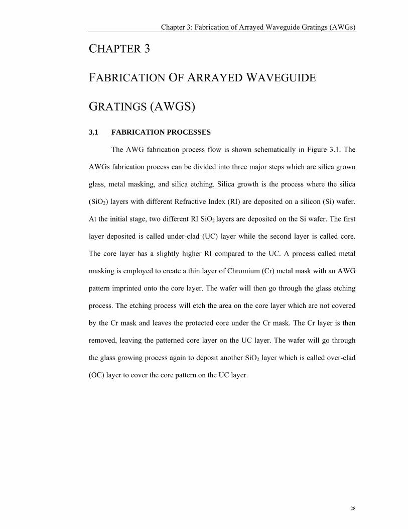
The AWG fabrication process flow is shown schematically in Figure 3.1. The
AWGs fabrication process can be divided into three major steps which are silica grown
glass, metal masking, and silica etching. Silica growth is the process where the silica
(SiO2) layers with different Refractive Index (RI) are deposited on a silicon (Si) wafer.
At the initial stage, two different RI SiO2 layers are deposited on the Si wafer. The first
layer deposited is called under-clad (UC) layer while the second layer is called core.
The core layer has a slightly higher RI compared to the UC. A process called metal
masking is employed to create a thin layer of Chromium (Cr) metal mask with an AWG
pattern imprinted onto the core layer. The wafer will then go through the glass etching
process. The etching process will etch the area on the core layer which are not covered
by the Cr mask and leaves the protected core under the Cr mask. The Cr layer is then
removed, leaving the patterned core layer on the UC layer. The wafer will go through
the glass growing process again to deposit another SiO2 layer which is called over-clad
(OC) layer to cover the core pattern on the UC layer.

Chapter 3: Fabrication of Arrayed Waveguide Gratings (AWGs)
29
Figure 3.1: Process flow for the AWGs fabrication
3.2 GLASS FABRICATION
There are large numbers of deposition methods that can be adopted to deposit
the thick glass layers required for silica-on-silicon integrated optics. These include
thermal oxidation and nitridation, sputtering, chemical vapour deposition (CVD),
plasma-enhanced chemical vapour deposition (PECVD), flame hydrolysis depositions
(FHD), sol-gel deposition (SGD) [1, 2]. The most commonly used methods nowadays
are PECVD and FHD. In this research, FHD is the chosen method to fabricate the
AWGs. FHD is a promising method due to its high deposition rate at low production
cost to gain a thick silica glass layer which can be loaded with other dopants such as Ge,
B, P, and Ti [3, 4].
The glass growing process is done by the combination of FHD porous silica
glass “soot” deposition and furnace consolidation. In FHD, the metal chlorides material
such as SiCl4, POCl3, BCl3, and GeCl4 (act as a dopant and not necessary in every
deposition) are vaporized under bubbling technique with He or O2 as carrier gases. A
mixture of raw gaseous metal chloride materials will experience hydrolysis and
oxidation in the high temperature oxy-hydrogen torch flame (1300-1500oC) which is
directed towards the samples. The deposition is done by thermophoretic mechanism
where the metal oxide particles are nucleated by the hydrolysis reaction, cohered by the

Chapter 3: Fabrication of Arrayed Waveguide Gratings (AWGs)
30
Brownian motion, and then synthesized in polydisperse particles [5]. The hydrolysis
and oxidation reaction of metal chloride materials to form the silica glass soot layer is
summarized in Table 3.1 [5, 6]:
Table 3.1: Hydrolysis and oxidation reaction of metal chloride materials Material Product and chemical reaction Effect
Silicon Pure silica glass (SiO2)
SiCl4(v)+2H2O(v)→SiO2(s)+4HCl(v)
None
Phosphorous Phosphosilicate glass (SiO2:P2O5)
2POCl3(v)+3H2O(v)→P2O5(s)+6HCl(v)
Thermal expansion: increase
Glass melting point: decrease
Refractive index: increase
Boron Borosilicate glass (SiO2:B2O3)
2BCl3(v)+3H2O(v)→B2O3(s)+6HCl(v)
Thermal expansion: increase
Glass melting point: decrease
Refractive index: decrease
Germanium Germanosilicate glass (SiO2:GeO2)
GeCl4(v)+2H2O(v)→GeO2(s)+4HCl(v)
Thermal expansion: increase
Glass melting point: decrease
Refractive index: increase
* H2O is the result of oxy-hydrogen flame where 2H2 (v) + O2 (v) → 2H2O (v)
The porous silica glass soot needs to be consolidated before it become hard and
transparent as a silica glass. The consolidation process includes a few temperature steps
for certain reason. First stage, the silica will be heated at 200oC for dehydration to
remove water or H2O. The removal of H2O will reduce the water absorption peak in
silica significantly. Then the temperature will be ramped up to 850oC and is held for
~30 minutes for bubble out-gassing. This step will prevent the formation of bubbles
(pores) at the silica glass. After that, the temperature will be ramped up to ~1300oC for
consolidation process. In consolidation process, the silica glass soot is melted into
viscous liquid form. Finally the temperature will start to ramp down as the glass molten
is slowly quenched into a final transparent glass coating.

Chapter 3: Fabrication of Arrayed Waveguide Gratings (AWGs)
31
3.3 METAL MASKING
Metal masking is a series of processes to create a metal mask pattern on the
surface of silica layer. The usage of the metal mask is to protect the needed core layer
during glass etching in later processes. Metal masking starts from chromium (Cr) thin
film deposition, followed by photolithography, and finally Cr wet etching. The Cr thin
film deposition is done by using Direct Current (DC) magnetron sputtering system to
deposit a layer of Cr thin film which is thick enough to protect the core layer in glass
etching later. Details of Cr deposition will be discussed later in Chapter 4.
Photolithography is the process where the pattern from the photomask (original copy
pattern) is transferred to the photoresist (PR) on the Cr thin film. The pattern transfer
processes include PR coating, Ultra-Violet (UV) exposure, and PR developing.
Photolithography will also be discussed in more detail in Chapter 5. The last part of the
metal masking is the Cr etching process. The etching method of choice is wet etching
which depends on the chemical reaction of the chemical on Cr thin film. The chemical
reaction will etch away the areas not covered by Cr thin film and leave those parts
which are covered by the PR. Details of Cr etching will also be discussed in Chapter 6.
The PR will then be removed by using acetone stripping, leaving the Cr mask behind.
The process flow of metal masking is shown in Figure 3.2.
Figure 3.2: Process flow for the metal masking

Chapter 3: Fabrication of Arrayed Waveguide Gratings (AWGs)
32
3.4 GLASS ETCHING
Glass etching is often divided into two classes, wet etching and dry etching. Wet
etching consists of chemical reaction between the etchant and the glass and it is
normally done by immersing or bath technique. Wet etching is an isotropic etching
technique which is difficult to control and prone to high defect level. Problems like
undercut, rough surface and high etch bias will always exist in wet etching. Dry etching
or normally called plasma etching is an anisotropic etching. Dry etching can be done by
chemical reaction between the gaseous etchant and the glass layer or by physical
etching using ion bombardment to erode the glass layer. Dry etching carries the
advantages of less sensitivity to temperature, high repeatability, no undercut, and less
chemical waste [7, 8].
In this research, Inductively Coupled Plasma (ICP), which is one of the plasma
etching method, is chosen for the silica core etching. ICP has the advantages of high
etch rate, cleaner, higher selectivity, and lower surface damage due to the lower
operating energy compared to other plasma etching techniques. CF4 that is used in the
ICP as an etchant gas will react with the silica layer as:
In plasma condition, CF4 + e → CF3+ + Fo +2e
SiO2 + 4F → SiF4 + O2
Generally, SiO2 (s) + CF4 (g) → SiF4 (g) + CO2 (g) (3.1)
The reaction shows above will remove the unwanted area of silica layer leaving
behind those areas which cover by the Cr mask.

Chapter 3: Fabrication of Arrayed Waveguide Gratings (AWGs)
33
3.5 SUMMARY
In this chapter, the main parameters related to sputter deposition,
photolithography, and etching were studied. These parameters are specific to the
equipments employed and are therefore, unique to the processes we use here. The
production yield and Critical Dimension (CD) of the fabrication process by using the
original fabrication recipe and method are unfortunately extremely low. The production
yield of the complete Cr hard mask pattern is below 40% and the CD of the Cr pattern is
totally out of the measurement scale printed on the AWG photomask. Optimization of
these important parameters is essential in order to produce commercialize grade AWGs.
Table 3.2 shows the important parameters in these three process mention above.
Table 3.2: Important parameters in different processes Process Parameters Important
Sputter
Deposition
- Thickness
- Uniformity
- Roughness
- Chemical stability
- To protect the core layer in glass etching.
- To increase the uniformity in wet etching.
- To reduce the pinhole defect in ICP
etching.
- To optimize the wet etching process in
order to improve the production yield.
Photolithography - PR Thickness
- PR Uniformity
- Critical Dimension
- To protect the Cr pattern area in wet
etching.
- To reduce the effect of depth of focus
when
UV expose.
- To maintain the original pattern
dimension.
Wet Etching - Critical Dimension
- Side Wall Angle
- Side Wall
Roughness
- To maintain the original pattern
dimension
- To create a rectangular core pattern.
- To create a smooth core side wall.

Chapter 3: Fabrication of Arrayed Waveguide Gratings (AWGs)
34
REFERENCES
[1] Wu, Y. D., Xing, H., Zhang, L. T., Li, A. W., Zheng, W., Liu, G. F., et al.
(2004). Fabrication and Properties of Vitreous Silica Films Prepared by Flame
Hydrolysis Deposition. Material Chemistry and Physics, 84, 234-237.
[2] García-Blanco, S., Glidle, A., Cooper, J. M., De La Rue, R. M., & Aitchison, J.
S. (2004). Characterization of Germanium-Doped Silica Layers Deposited by
Flame-Hydrolysis. Optical Material, 27, 365-371.
[3] Zhang, L., Xie, W., Xie, W. F., Hou, Y., Zheng, W., & Zhang, Y. (2004).
Characterization of Ge-Doped Silica Films with Low Optical Loss Grown by
Flame Hydrolysis Deposition. Materials Science and Engineering B, 107 (3),
317-320.
[4] Zhang, L., Xie, W., Wu, Y., Xing, H., Li, A., Zheng, W., & Zhang, Y. (2003).
Optical and Surface properties of SiO2 by Flame Hydrolysis Deposition for
Silica Waveguide. Optical materials, 22, 283-287.
[5] Choi, C. G., Jeong, M. Y., & Choy, T. G. (1999). Characterization of
Borophophosilicate Glass Soot Fabrication by Flame Hydrolysis Deposition for
Silica-On-Silicon Device Applications. Journal of Material Science, 34, 6035-
6040.
[6] Sonia, G. B., & Aitchison, J. S. (2005). Direct Electron Beam Writing of Optical
Devices on Ge-Doped Flame Hydrolysis Deposition Silica. Journal of Selected
Topics in Quantum Electronics, 11 (2), 528-538.
[7] Sami Franssila (2004). Introduction to Micro Fabrication. England: John Wiley
& Sons.
[8] Campbell, S. A. (2001). The Science and Engineering of Microelectronic
Fabrication (2nd ed.). New York: Oxford University Press.

Chapter 4: DC Magnetron Sputter Deposition
35
CHAPTER 4
DC MAGNETRON SPUTTER DEPOSITION
4.1 BACKGROUND
Sputtering or physical sputtering (pulvérization in French) involve the
vaporization of target by momentum transfer as a result of ions bombardment at the
target surface. It was first observed by Groove in 1852 and Pulker in 1858 using von
Guericke-type oil-sealed piston vacuum pumps [1]. Sputter deposition is just the
accumulation of sputtered atoms which are dislodged from the target (cathode) surface
onto a substrate. The sputter deposition is random where not only the substrate will be
deposit but the whole surrounding surface. Sputter deposition of films was first reported
by Wright in 1877 with a relatively poor vacuum. A sputter deposition process to
deposit silver onto wax photograph cylinder was patented by Edison in 1904 [1]. The
wide usage of sputter deposition in industry began when the needed of the deposition
process to be reproducible especially in semiconductor fabrication. The development in
sputter deposition process continued until today with a few different methods like diode
sputter deposition, reactive sputter deposition, bias sputter deposition, ion beam sputter
deposition, and more [2].
Magnetron sputter deposition is one of the variant from sputter deposition
sources which uses magnetic fields transverse to the electric fields at sputtering-target
surfaces. Planar magnetron sputtering was derived from the development of the
microwave klystron tube during world war two, the work of Kesaev and Pashkova
(1959) in confining arcs and Chapin (1974) in developing the planar magnetron
sputtering source [1]. From here the applications of magnetrons with plasma-based
sputtering application were developed. The most useful description available has been

Chapter 4: DC Magnetron Sputter Deposition
36
the work of Thornton and Penfold, in Vossen and Kern’s book dating from the late ‘70s
[3].
4.2 THEORY OF SPUTTERING
4.2.1 SPUTTERING AND SPUTTER DEPOSITION PROCESSES
As mentioned in the introduction, sputtering is a process that involves the
vaporization of surface atoms by the bombardments of incident ions. The incident ions
are normally generated by plasma or glow discharge. The incident ions will then
accelerate towards the cathode surface electrically [2]. The bombardment between the
incident ion and the surface atom results in energy transfer, similar to the physical
collision between two hard spheres (considered as elastic collision) as shown in Figure
4.1.
Figure 4.1: Elastic collision between two hard spheres
The energy transfer process consider two important laws below,
Conservation of Momentum,
ttiittii vmvmumum +=+ (4.1)
Conservation of Energy,
2222
21
21
21
21
ttiittii vmvmumum +=+ (4.2)
where m is the mass, u is the initial velocity, v is the final velocity, i represents incident
ion, and t represent target ions.

Chapter 4: DC Magnetron Sputter Deposition
37
By solving the equations 4.1 and 4.2, the energy of the incident ion is relate to
the energy transfer by,
2
2
)(cos4
ti
ti
i
t
mmmm
EE
+=
θ (4.3)
where E is energy, m is the mass, u is the initial velocity, v is the final velocity, i
represents incident ion, t represents target particles (surface atoms), and θ = angle of
incidence as measure from a line joining their centers of masses as shown in Figure 4.2.
Figure 4.2: Collision of two particles
The bombarding effect can physically penetrate into the surface region and
creates a series of collisions among the atoms near the surface. Surface atoms will break
the bonding and dislodge when they gain enough energy from the collisions. All the
removed atoms from the surface are considered as sputtered atoms [2]. This physical
sputtering process is shown in Figure 4.3. The number of sputtered atom for each
bombardment of an incident ion is called sputter yield, Y = (number of sputtered atoms/
number of incident ions). Sputter yield is dependent on the energy transfer as mentioned
earlier. Most of the transferred energy (>95%) appears as heat in the surface region and
near-surface region [1].

Chapter 4: DC Magnetron Sputter Deposition
38
Figure 4.3: Schematic of a physical sputtering process
4.2.2 DC MAGNETRON SPUTTER DEPOSITION
Magnetrons are a class of cold cathode discharge devices used generally in
diode mode. In DC diode sputtering, secondary electrons are generated from the
cathode due to the bombardments by the surrounding ions. These electrons are
accelerated toward the anode and ionize the surrounding atoms by collision. However
these ionizations are not efficiently use for sustaining the discharge. Furthermore the
secondary electrons that reach the anode will bombard on the substrate that is held on
the anode. These bombardments will increase the substrate temperature and cause
radiation damage [2].
A magnetron sputtering is designed to overcome all the above issues. A
magnetron cathode which a static magnetic field configured at the cathode location is
used in magnetron sputtering system. There are a few types of magnetron in the market
as shown in Figure 4.4.

Chapter 4: DC Magnetron Sputter Deposition
39
Figure 4.4: Various types of magnetron cathode (Picture taken from [2])
Among those, the planar magnetron is the most common magnetron where the
sputter-erosion path is a close circle or elongate circle (“race-track”) on the target or
cathode surface. To create the magnetic field that is parallel to the cathode surface, the
pole piece assembly is placed behind the cathode. The local polarity of the magnetic
field in the magnetron is oriented such that the ExB will drift the secondary electron in
the desired closed loop depending on the design. The ExB that drifts the secondary
electron can be explained by Hall Effect. The electric field direction, E is always
perpendicular to the cathode surface while the magnetic field direction, B depends on
the design. According to Hall Effect, if an electric current flows through a conductor in
a magnetic field, the magnetic field exerts a transverse force on the moving charge
carriers. The path that the electrons follow can be predicted using the right-hand rule.
Figure 4.5 shows the secondary electrons drift path under the influence of the circular
planar magnetron cathode.

Chapter 4: DC Magnetron Sputter Deposition
40
Figure 4.5: Magnetic field configuration for a circular planar magnetron cathode (Picture taken from [2])
The secondary electrons that were accelerated inside the closed loop will
experience frequent collisions with atoms of the background gas and this creates a high
discharge density near to the cathode surface. Thus, high discharge density can be
sustained even with lower chamber pressure down to 1 - 2 mTorr compared to the
general diode sputtering which need at least 15 mTorr[3]. The low operation pressure
will significantly reduce the scattering of the sputtered atoms by the background gas on
the way to the sample. This results in the increased probability for the sputtered atoms
to reach the substrate and the increasing of the average kinetic energy of the sputtered
atom. The high density of discharge also means that a high sputtering rate can be
achieved, resulting in higher deposition rate. Besides that, the secondary electrons that
were trapped inside the circle trajectory will not contribute to the increase of the
substrate temperature and radiation damage as they do not bombard the substrate at the
anode [2].

Chapter 4: DC Magnetron Sputter Deposition
41
4.3 DC MAGNETRON SPUTTERING SYSTEM AND PROCESS
METHODOLOGY IN PHOTONIC RESEARCH CENTRE (PRC)
4.3.1 WAFER LOADING AND UNLOADING IN LOAD-LOCK SYSTEM
PRC own dc magnetron sputtering system is designed to have two different
chambers, one is called process chamber and the other one is call load-lock chamber as
shown in Figure 4.6. Both chambers are connected to each other but the process
chamber is isolated from the load-lock chamber by a load-lock gate valve. The process
chamber is where the sputtering and the sputter deposition processes take place, while
the load-lock chamber is where the loading and unloading of samples is performed.
To load a wafer into the process chamber, the wafer must be cleaned beforehand
(using the cleaning procedures discussed in Appendix B) to reduce the contamination
on the wafer surface and the chamber environment. Argon (Ar) gas is supplied into the
load-lock chamber to increase the pressure in the load-lock chamber until it reaches
atmospheric pressure. The clean wafer is then placed onto a mechanical arm in the load-
lock chamber through the loading door. The load-lock chamber will then be pumped
down with a rotary pump until the pressure is below 1x10⁻² Torr to match the process
chamber pressure which is always kept below 1x10⁻² Torr. The chamber pressure is
measured using a Pirani gauge.
Pressure matching is very important because when the load-lock gate valve open,
a pressure difference between both chambers will create air flow that might displace the
wafer. The wafer is delivered into the process chamber by the mechanical arm and is
then unloaded onto a substrate stage in the process chamber after the load-lock gate
valve is opened. The load-lock gate valve is then closed to isolate the process chamber
from the load-lock chamber. Thus, with the load-lock system, the pressure of the
process chamber can be kept below 1x10⁻² Torr all the time for wafer loading and
unloading.

Chapter 4: DC Magnetron Sputter Deposition
42
Figure 4.6: DC magnetron sputtering system chamber
There are a few advantages of the load-lock system compared to loading the
wafer into the process chamber directly from ambient. The main advantage is to reduce
the contamination by the water vapor from ambient to the process chamber. Due to the
process chamber not directly exposed to the ambient, the chances for the water vapor
from ambient to be adsorbed by the system inner surface are highly reduced. Secondly,
this system reduces the time needed for the chamber to pump down to pressure below
1x10⁻² Torr after exposure to the ambient due to the smaller volume of load-lock
chamber compared to the process chamber, thus reducing the process duration.
4.3.2 PRC DC PLANAR MAGNETRON SPUTTERING SYSTEM
The process chamber consists of a cylindrical chamber, a substrate holder
(anode) with shutter, and a planar magnetron cathode behind the Chromium (Cr) target
(sputtering or deposition material). Besides that, the process chamber is also connected
to an Ar gas inlet which is used as the background gas, a Turbo Molecular Pump (TMP)
that is supported by the rotary pump, and three pressure gauges (one pirani gauge, one
baratron gauge and one ion gauge).

Chapter 4: DC Magnetron Sputter Deposition
43
a) Cr thin film as silica etching mask and Cr target design
Cr thin film or Cr mask plays an important role in glass etching process for
planar waveguide fabrication. The Cr layer is patterned according to the designed
waveguide circuitries on the silica layer to cover the wanted silica area in the silica
etching process. Silica etching process is normally done either by HF (isotropic etching)
or Reactive Ion Etching (RIE) (anisotropic etching). Metal mask is needed for high
etch depth (5-10μm) for silica RIE process in the planar waveguide fabrication. A metal
mask carry advantages like low temperature deposition process, easy patterning of the
layer by lithography and wet etching solutions and easy removal of the mask after the
glass etching. A Cr etching mask is selected since it adheres to silica film well and is
strong enough to resist the bombardment of the reactive gas and Ar+ ions in the
discharge during an etching process of long duration, typically 40 minutes [4, 5].
Cr 4 inch target was used to match the circular planar magnetron cathode in the
system. The purity of the Cr target is up to 99.99% to avoid contamination from
unwanted materials. Besides that, the target was also designed to contain “racetrack”
depression on the surface to increase the deposition uniformity. In magnetron sputtering,
the erosion of the target is not uniform. The erosion is based on the concentration of the
magnetic field. Thus, the racetrack design not only increases the deposition uniformity,
it will also increase the utilization of the target.
b) Ar gas as background gas
The main consideration of taking Argon gas as the background gas is because it
is an inert gas which is stable and hardly reacts with other materials. Among the inert
gases, Ar is chosen based on its mass. From equation 4.3, notice that the energy transfer
is highly dependent on the mass of the incident particle. The higher the incident mass,
the higher the energy transfers (if the collision angle is neglected). Inert gases like He

Chapter 4: DC Magnetron Sputter Deposition
44
and Ne are not considered as their atomic mass is too small compared to Cr. Inert gas
like Kr is also not considered due to its atomic mass being too heavy. Although heavier
ions are more efficient in transfer energy, they will also scattered away the sputter
atoms that are moving towards the wafer and hence affect the deposition process.
c) Magnetron cathode with water cooling circulation
The magnetron gun is attached to a water circulating system. As mentioned in
section 4.2.1, more than 95% of the energy transferred to the sputtering target will
appear as heat. The water circulating system keeps the Cr target cool during the
deposition process. The cold surface will minimize the amount of radiant heat in
sputtering systems which benefit the thermal evaporation in vacuum. Thus, even
thermally-sensitive surfaces can be placed near the sputtering target. Besides that,
cooling also prevents diffusion in the target which will lead to changes in the elemental
composition for alloy targets [1].
d) Turbo molecular pump (TMP) supported by a rotary pump
In the process chamber, pressure is maintained under “rough” vacuum
environment (10-2 Torr) by using a rotary pump. To reach a “good” vacuum (10-6 Torr)
environment which is clean enough from process contamination, TMP is used to pump
the chamber pressure further. Normally TMP is operated in the “rough” vacuum
environment as TMP cannot tolerate abrasive particles or large objects due to the close
tolerances in mechanical parts (especially between rotor blades in TMP). Thus, to create
a rough vacuum environment, TMP is always backed by a rotary pump. A disadvantage
of TMP is the poor pumping ability for water vapor since the water molecules will
undergo numerous adsorptions-desorption events before passing through the pump. This
is one of the reasons why the load-lock system is used to reduce the adsorption of the

Chapter 4: DC Magnetron Sputter Deposition
45
water vapor from the ambient. The advantages of choosing TMP includes non
contamination of motive fluid, omission of high-vacuum valve, lower probability of
back streaming accidents, and it pumps all gases effectively[6].
4.3.3 CHROMIUM SPUTTER DEPOSITION PROCESS METHODOLOGY
After the wafer is loaded onto the substrate holder, the shutter above it is closed
to protect the wafer from deposition before the grow discharge is stable. Ar and N2 (N2
is needed for all the valve operation) pressure and supply is ensured to be sufficient for
the whole process and the water circulation is necessary for the magnetron gun. TMP is
backed by the rotary pump before it switches on. The process chamber is then pumped
by TMP after it reached the maximum spin speed (27000rpm).
After the process chamber reaches a pressure below 10-6 Torr, Ar gas is flown
into the process chamber forming the background gas for the sputtering process. The
flow rate of the gas Ar is controlled by MFCs (Mass Flow Controllers) in sccm
(Standard Cubic Centimeters per Minute) units. The process chamber pressure is set
using the pressure controller which obtains the feedback from a baratron gauge that
connects to the process chamber. Then the pressure controller will control the opening
percentage of the throttle valve to maintain the pressure inside the process chamber.
The process chamber pressure will be stable after a few minutes adjustment by
the pressure controller. DC power supply voltage is increase until the breakdown
voltage and the grow discharge is generated. The DC breakdown voltage can be
calculated by using the following equation
)]ln([
)(PdC
PdAV+
= (4.4)
where V is the DC voltage, A and C are constants depending on the gas used, P is the
chamber pressure, and d is the distance between the cathode and anode [7]. Figure 4.7
shows the glow discharge near the target.

Chapter 4: DC Magnetron Sputter Deposition
46
Figure 4.7: Grow discharge at target surface
Figure 4.7 clearly shows that the glow discharge form a circular loop at the
target surface. The brightest ring tells the concentration of the magnetic field. After the
glow discharge has been generated, it will take a few minutes for the discharge to
become stable, and this can be observed from the reading of the power supply. Within
this period, the wafer is covered under the shutter to prevent from deposition, which is
referred to as pre-sputtering process. The purpose of pre-sputtering process is to remove
the oxide layer or contaminants which cover the target surface. When the DC power is
first applied to the Cr target, the power will be high and will eventually drop as the
discharge comes to equilibrium. The initial high power is due to the high secondary
emission of the metal oxide as compared to the clean metal and the high density of the
cold gas. As the oxide is removed from the surface and the gas heats up, the power will
drop [1]. After the pre-sputtering process, the deposition process is ready to commence.
After the deposition, the DC power supply voltage is reduced slowly to 0V. The
Ar gas supply is then stopped flowing in and the TMP gate valve is closed.

Chapter 4: DC Magnetron Sputter Deposition
47
4.3.4 PUMP PURGE CYCLES AFTER DEPOSITION
After the deposition, pump purge cycles are applied to remove the remaining
particles in the process chamber before the wafer is taken out into the load-lock
chamber. The particles can be produced in the process chamber by many sources,
including when wafer loading, the impurities gas supply, and also process chamber
leakage. During the deposition process, these particles do not generally cause
processing problems as they are typically suspended above the wafer in the plasma due
to the electrostatic interaction. However, as the power reduces at the end of the
deposition process, the forces that suspend the particles dissipate allowing them to fall
and land on the wafer causing contamination. To avoid this problem, pump purge cycles
are applied to remove the remaining particles. During pump purge cycles, Ar gas is
supplied into the process chamber until the pressure increases to 10mTorr. After this
pressure is reached, Ar supply will be stopped and the TMP gate valve will be opened
to pump down the process chamber. This rapid removal of the Ar gas will create
turbulence which has a sweeping effect carrying particles with the escaping Ar gas
outside the process chamber [8]. This cycle will be repeated 3 times to make sure that
most of the particles are removed before the wafer is unloaded into the load-lock
chamber.
4.4 EXPERIMENTAL RESULTS AND DISCUSSIONS
Thickness, uniformity, surface roughness, and chemical stability of the Cr thin
film are the main issues to create a quality hard mask for glass etching process. Low
quality hard mask will creates problems like low production yield (<40% for original
process recipe) and poor Critical Dimension (CD). Studies are done on each process
parameters to determine their effect on those critical issues mentioned above. A process
recipe for better production result will be produced in this study.

Chapter 4: DC Magnetron Sputter Deposition
48
4.4.1 STUDY OF DEPOSITION TIME
The Cr depositions are run under fix DC power (0.8A) (*voltage of power
supply is not considered as it is current control in plasma), substrate temperature (30°C),
Argon flow rate (5sccm), and process chamber pressure (10mTorr). Wafer is covered
with a simple mask when deposition for thickness measurement. Thickness of the Cr
layer was measure at multiple points on the wafer by using surface profiler (Alpha-Step
2000) and plotted in the graph shown in Figure 4.8.
Figure 4.7 shows a linear increment of the Cr thickness with the increase of time.
From the gradient of the graph, the deposition rate of Cr is 43nm/minutes. From the raw
data, it shows ±15% variants of Cr thickness from the mean value which is plotted in
Figure 4.8. The non-uniformity of Cr thickness is mainly cause by the target design. As
mention in the previous section, the target is design with “racetrack” depression to
increase the uniformity. Unfortunately, the uniformity of the deposition will still
degraded after a certain period due to the changes of the “racetrack” causes by
sputtering.
Figure 4.8: Cr thickness for different sputtering time

Chapter 4: DC Magnetron Sputter Deposition
49
Figure 4.9 shows the change of the grains size due to the increment of the Cr
thin film thickness. The surface morphology of Cr thin film was inspected using AFM
(atomic force microscopy) to study the change of the grain height due to the Cr
thickness. The AFM images for Cr thin film with (70±5) nm and (330±5) nm thickness
are shown in Figure 4.10. For thinner Cr layer, the average grain size is smaller thus the
surface is smoother in Figure 4.10(a). When the Cr thickness increases, the grains grow
and agglomerated together, resulting in less number of bigger grains as shown in Figure
4.10(b). The grains growth can be explained by the surface energy minimization during
the growth process to achieve thermodynamic equilibrium. The growth directions of the
grains are toward a situation of low surface energy [9, 10].
Figure 4.9: Increment of Cr grains height according to thin film thickness
Chemical stability was studied by observing the etching rate of Cr thin film
under the reaction with Cr etchant (Cr-7S). The wafer is place in the Cr etchant until the
Cr thin film is totally removed (*details about Cr etching will be discussed in Chapter
6). During the etching process, we observe that the etching normally finish at the edge
of the wafer and proceed slowly to the center. The period for the etching process to be
start at the edge and period for the whole etching process were taken down and plotted
in the graph in Figure 4.11.

Chapter 4: DC Magnetron Sputter Deposition
50
a)
b)
Figure 4.10: AFM images of Cr thin film for a) (70±5) nm and b) (330±5) nm thickness

Chapter 4: DC Magnetron Sputter Deposition
51
The time for the Cr to be removed at the edge increases quite linearly with the
Cr thin film thickness. This is expected as more time is needed for etching a thicker Cr.
However the time needed for the Cr of the whole wafer to be removed increases non-
linearly with the Cr thickness. The higher exposure area and less inner bonding make
the etching process to be faster at the edge of the wafer compared to the center area [11].
This causes a time difference for the etching to finish at the edge of the wafer until the
etching process is done for the whole wafer as shown in Figure 4.11. The center area of
the wafer needed nearly double the time compare to the edge of the wafer to complete
the etching process.
Figure 4.11: Etching time for different Cr thickness
4.4.2 DC CURRENT EFFECT ON CHROMIUM DEPOSITION
In this section, the relation of voltage-current in DC power supply and the effect
of DC current supply is presented. The voltage-current relation in DC magnetron
sputtering system in University of Malaya is shown in Figure 4.12. From Figure 4.12, it
is noticed that the voltage increase quite significantly when the current increase. This is
quite different from a normal glow discharge where the voltage is independent of the

Chapter 4: DC Magnetron Sputter Deposition
52
total current. In an abnormal glow discharge, the voltage increases significantly to force
the cathode current to increase above its natural value to produce enough secondary
electron for sputtering process [12]. The further increase of the current might causes the
transition of abnormal glow discharge to arc discharge (glow-to-arc transition) which
we do not want it to happen.
Figure 4.12: The voltage and current as a function of total current drawn by DC glow discharge
Study of DC current effect on Cr deposition is done by a series of deposition
with current, Idc from 0.5A to 1.2A. Figure 4.13 shows the Cr thin film thickness with
various DC power supply current, Ic, with deposition time of 5 minutes. The Cr thin
film thickness increases linearly with the Ic. This corresponds to a linear relation
between the Cr thin film deposition rate and Ic. This phenomenon can be explains from
Child’s law and the sputtering rate. The deposition rate is proportional to the sputtering
rate because the sputtering rate decides the number of sputtered Cr atoms from the Cr
target.

Chapter 4: DC Magnetron Sputter Deposition
53
From the equation of sputtering rate, Rsput,
scmne
JR
Cr
isputsput /1γ= (4.5)
where γsput is the sputtering yield, Ji is the ion current density, and nCr is the atomic
density of Cr target [13]. Thus Rsput α Ji in a more simplify form.
Due to the demagnetized of the ions and the design of the magnetron sputtering
which operate in low pressure, non-collision Child’s law can be used to describe the
flow of ions from the surface to the ring of cathode. By assuming that w << R,
Rw
IJ dc
i π2= (4.6)
where Idc is the DC power supply current, R is the radius from the target center to the
magnetic ring, and w is the width of the magnetic field on the cathode [13]. Equation
(4.5) and (4.6) shows the relation that sputtering rate, Rsput is proportional to DC power
supply current, Idc which explain the experimental results. The graph in Figure 4.13
give a linear graph gradient of approximately 260nm/A for 5 minutes. In another word,
an increment of deposition rate of 52nm/minutes per Ampere (A) increase.
Figure 4.13: Cr film thickness with DC power supply current, Idc
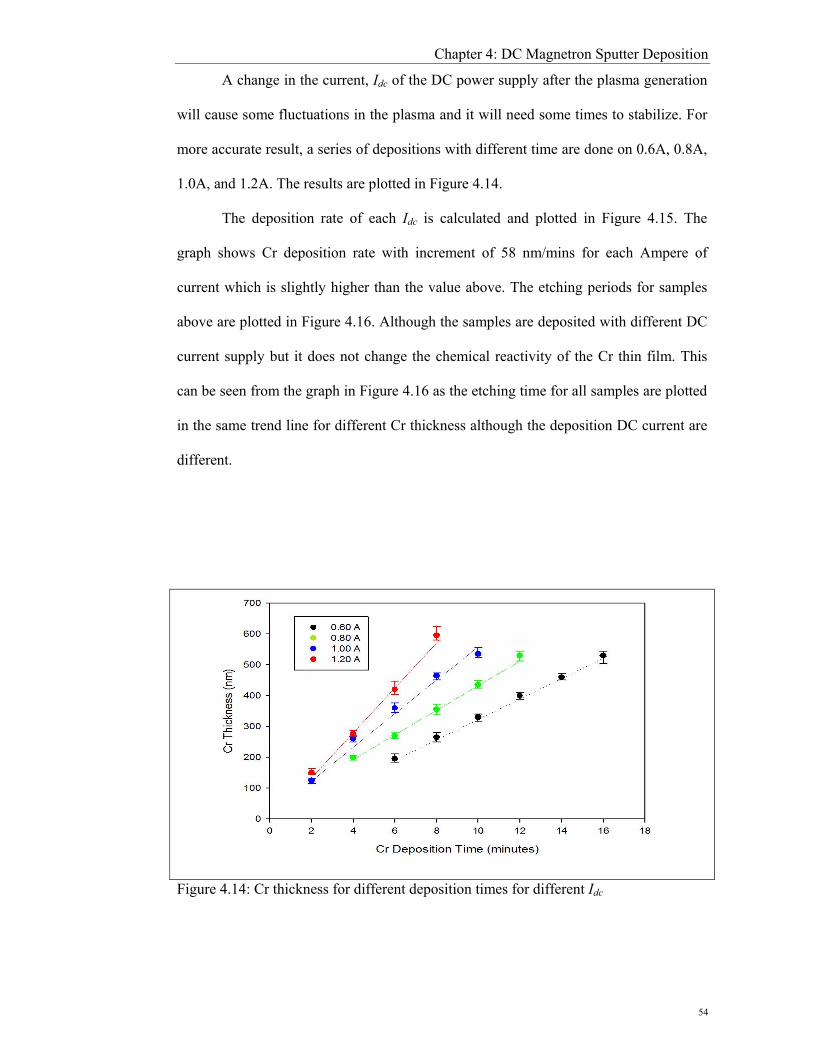
Chapter 4: DC Magnetron Sputter Deposition
54
A change in the current, Idc of the DC power supply after the plasma generation
will cause some fluctuations in the plasma and it will need some times to stabilize. For
more accurate result, a series of depositions with different time are done on 0.6A, 0.8A,
1.0A, and 1.2A. The results are plotted in Figure 4.14.
The deposition rate of each Idc is calculated and plotted in Figure 4.15. The
graph shows Cr deposition rate with increment of 58 nm/mins for each Ampere of
current which is slightly higher than the value above. The etching periods for samples
above are plotted in Figure 4.16. Although the samples are deposited with different DC
current supply but it does not change the chemical reactivity of the Cr thin film. This
can be seen from the graph in Figure 4.16 as the etching time for all samples are plotted
in the same trend line for different Cr thickness although the deposition DC current are
different.
Figure 4.14: Cr thickness for different deposition times for different Idc

Chapter 4: DC Magnetron Sputter Deposition
55
Figure 4.15: Cr deposition rate on different DC current supply, Idc
Figure 4.16: Cr etching rate for different Cr thickness coated with different current

Chapter 4: DC Magnetron Sputter Deposition
56
There are two lines in Figure 4.16, one show the time for the etching process
to be ended at the wafer edge while the other one shows the time for the etching
process to be ended at the wafer center. The etching time difference between the
wafer center and edge has create a huge issue in etching process. Due to the time
difference, pattern at the wafer edge was etched much longer compare to the time it
need. This is called over etch. Over etch will affect the pattern to experience series
undercut (more explanation in Chapter 6) which might destroy the Cr pattern and
cause low production yield (less than 40% in this case). Thus only pattern at the
center of the wafer can survive after the wet etching process.
4.4.3 PRESSURE EFFECT ON CHROMIUM DEPOSITION
In order to study the effect of process chamber pressure on the deposition
process, series of tests are run with different process pressure. Figure 4.17 shows the
DC power supply for different process pressure. It is clearly to observe that for lower
pressure, higher voltage need to be supply to maintain the current density in the glow
discharge condition. This can be explained by the equation of minimum discharge
voltage to sustain the magnetron discharge which proposed by Thornton [14]:
eiISEEei pEWW
Vεεγεγε )(
00min == (4.7)
where W0 is the effective ionization energy, εi is the ion collection efficiency, εe is the
fraction of the number of ions Vmin/W0 that can be made on average by primary electron
before it is lost form the system, and γ is the effective secondary electron emission yield
which is the product of ion-induced secondary electron emission (ISEE) coefficient
γISEE and the effective gas ionization probability E(p) [15].

Chapter 4: DC Magnetron Sputter Deposition
57
Figure 4.17: DC power supply for different process pressure
The effective gas ionization probability, E(p) is depends on the pressure and
recapture of the electrons. At low pressure, the chances for the electron to collide with
particles reduce and the probability of electron recapture (capture of electron back to
the cathode due to the applied magnetic field) is increase. This is due to the path length
of the electron become much smaller than the mean free path. Hence, the effective
secondary electron emission coefficient becomes smaller than the material dependent
ISEE coefficient. From equation 4.7, Vmin α 1/γ and hence when γ decrease, Vmin
increase. For higher pressure, the probability for electron recaptures decrease due to the
probability of collision with other particles increase. Recapture is prevented if the
electron undergoes a collision which deflects its trajectory by a sufficiently large angle
(> 10°) or lost in energy [16]. Thus electrons will continue circulate and collide. This
phenomenon increases the effective secondary electron emission coefficient and hence
the discharge voltage lower at higher pressure.

Chapter 4: DC Magnetron Sputter Deposition
58
Figure 4.18: Cr film thickness with different pressure deposition
Figure 4.18 shows the Cr thin film thickness that deposited with same DC
current supply but different pressure. The Cr thickness is quite consistence under such
condition with just a few nm difference between those samples. It shows that the
change in pressure did not give any significant effect on the Cr deposition rate. This is
due to the constant charge particles that maintain in the process chamber which already
explain in section 4.4.2.
However, the change of the process pressure did affect the properties of the
Cr thin film in the spec of chemical stability. Figure 4.19 shows the graph of etching
time difference between wafer center and wafer edge. Figure 4.19 shows that for
higher pressure, the time difference is higher compare to lower pressure. As we
know, the larger the difference time, the lower the pattern yield and poorer the
pattern CD. By changing the process pressure to 6mTorr, the pattern yield has
improve from around 40% to 100% where there do not have any part of the pattern is
totally etch out at the end of the etching process.

Chapter 4: DC Magnetron Sputter Deposition
59
Figure 4.19: Etching time difference between the wafer center and edge
4.5 SUMMARY
Cr thin film thickness control and chemical stability is very important as it
will affect the end result of the wet etching process especially yield and CD.
Thickness control was studied by varying the deposition time and DC current. The
Cr thin film thickness was directly proportional to the deposition time. The
deposition rate was determined by the DC current supply where each increase in
Ampere will increase the deposition rate at around 58nm/minutes. The study on
deposition pressure give a surprisingly result where it reduce the Cr etching time
difference between the wafer center and wafer edge. The significant reduction in the
time difference at 6mTorr pressure has resulted in an increased in the Cr pattern
yield from 40% to 100%.

Chapter 4: DC Magnetron Sputter Deposition
60
REFERENCES
[1] Mattox, D.M. (1998). Handbook of Physical Vapor Deposition (PVD)
Processing – Film Formation, Adhesion, Surface Preparation and Contamination
Control. Westwood, New Jersey, U.S.A.: Noyes Publications.
[2] Seshan, K. (2002). Handbook of Thin-Film Deposition Processes and
Technologies- Principles, Methods, Equipment and Applications (2nd ed.).
Norwich, New York, U.S.A.: Noyes Publications.
[3] Rossnagel, S.M., Cuomo, J.J., & Westwood, W.D. (1990). Handbook of Plasma
Processing Technology – Fundamentals, Etching, Deposition, and Surface
Interaction. Park Ridge, New Jersey, U.S.A.: Noyes Publications.
[4] Shin, D.W., & Eo, J.H. (2005). Plasma etching characteristics of Ge-B-P doped
SiO2 film for waveguide fabrication. Journal of Ceramic Processing Research, 6
(4), 345-350.
[5] Dutta, A.K. (1995). Side Wall Roughness Reduction in Deep Silicon Oxide
Etching Using C2F6 Based ECR-RIBE. Japan Journal Applied Physics, 34 (1),
365-369.
[6] Hablanian, M.H. (1997). High-Vacuum Technology: A Practical Guide (2nd ed.).
Marcel Dekker.
[7] Michael, A.L. & Allan, J.L. (1994). Principles of Plasma Discharges and
Materials Processing. New Jersey, U.S.A.: John Wiley & Sons.
[8] Mautz, K.E. (1999). Semiconductor Wafer Processing Chamber for Reducing
Particles Deposited onto the Semiconductor Wafer. United States Patent
5904800.
[9] Chan, K.Y. and Teo, B.S. (2006). Thickness dependence of the structural and
electrical properties of copper films deposited by dc magnetron sputtering
technique. Microelectronics Journal, 37, 608-612.
[10] Chan, K.Y. and Teo, B.S. (2006). Atomic force microscopy (AFM) and X-ray
diffraction (XRD) investigations of copper thin films prepared by dc magnetron
sputtering technique. Microelectronics Journal, 37, 1064-1071.
[11] Joseph A.M. (2003). Chemistry the Easy Way (4th ed.). Hauppauge, New York:
Barron’s Education Series.
[12] Roth, J.R. (1995). Industrial Plasma Engineering – Volume 1 (Principle).
London, UK: IOP Publishing Ltd.
[13] Michael, A.L. and Allan J.L. (1994). Principles of Plasma Discharges and
Materials Processing, United States of America: John Wiley & Sons.

Chapter 4: DC Magnetron Sputter Deposition
61
[14] Thornton, J.A. (1978). Magnetron sputtering: basic physics and application to
cylindrical magnetron. Journal of Vacuum Science and Technology, 15 (2), 171-
177.
[15] Depla, D., Buyle, G., Haemers, J., & Gryse, R.D. (2006). Discharge voltage
measurements during magnetron sputtering. Surface & Coating Technology, 200,
4329-4338.
[16] Gu, Q.C., Kunhardt, E.E., Levi, E., & Schaefer, G. (1989). The effect of
scattering on the recapture probability of secondary electrons by the cathode in
the presence of a magnetic field. Pulsed Power Conference, 798-800.

Chapter 5: Photolithography
62
CHAPTER 5
PHOTOLITHOGRAPHY
5.1 BACKGROUND
In this study, photolithography was used to create photoresist (PR) pattern on a
Chromium (Cr) layer after the layer deposition via sputtering. Photolithography is a
Latin word which means light-stone-writing [1]. It plays an important role in pattern
transfer processes. Photolithography was developed from lithography which was
invented by Alois Senefelder in Germany in 1798 [2]. First printing of lithography was
done by stone printing. Joseph Nicephore Niepce, in Chalon, France took the first
photograph in 1826 using bitumen of Judea on a pewter plate. The pattern was
developed using oil of lavender and mineral spirits. The first negative PR was
developed in 1935 by Louis Minsk of Eastman Kodak and followed by the development
of first diazoquinone-based positive PR in 1940 by Otto Suess of Kalle Div. of Hoechst
AG [1].
Photolithography was brought into semiconductor manufacturing sector for step
and repeat mask reduction devices since 1959 by using contact aligner. The contact
printing was the work-horse technology for exposing patterns onto Integrated Circuit
(IC) wafer well into the 1970 [3]. Since then, photolithography becomes widely used in
semiconductor manufacturing sector for mass production in fabrication of IC. This saw
the development of photolithography related devices such as stepper and mask aligner
in fulfilling the expanding IC market requirements.
The methodology used in photolithography and its processes determines the size,
weight, cost, reliability and capability of the fabricated device [4]. These variations are
mainly based on the PR used, coating method, and the UV exposure technique.
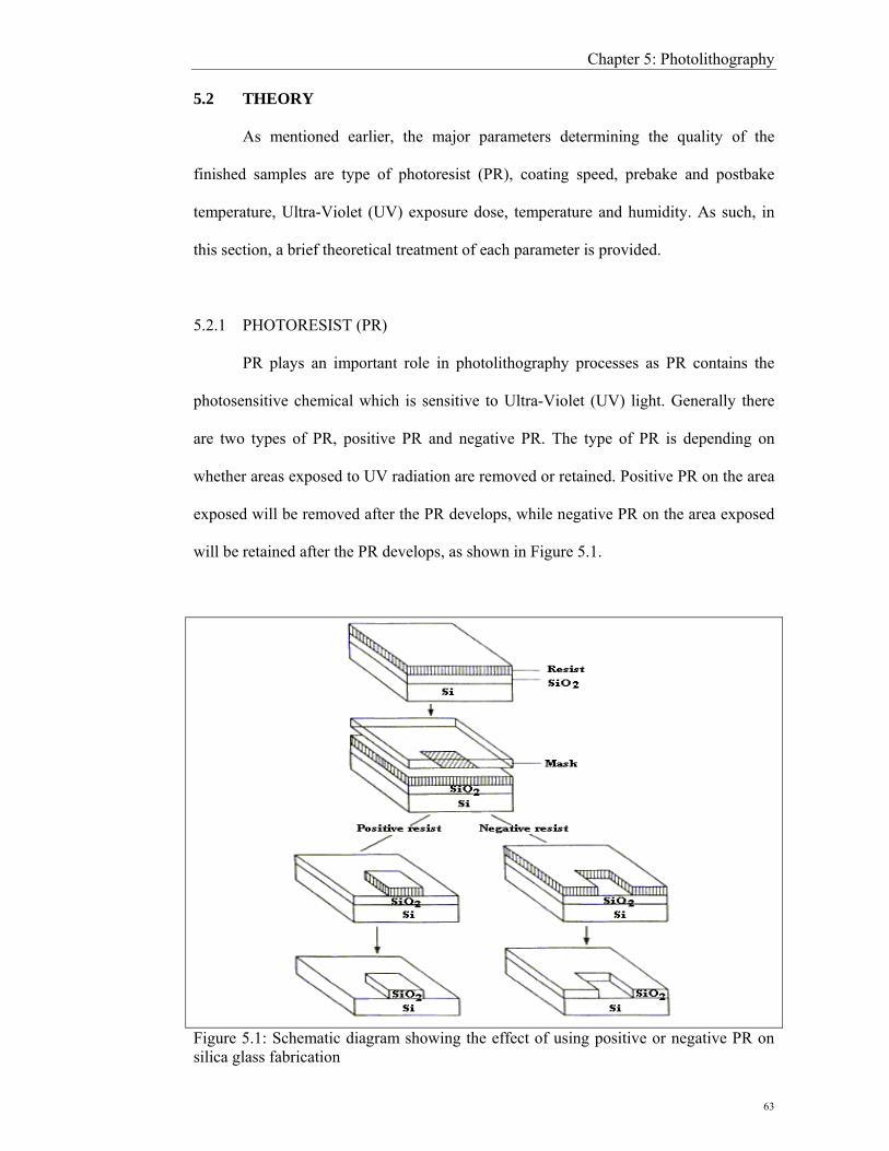
Chapter 5: Photolithography
63
5.2 THEORY
As mentioned earlier, the major parameters determining the quality of the
finished samples are type of photoresist (PR), coating speed, prebake and postbake
temperature, Ultra-Violet (UV) exposure dose, temperature and humidity. As such, in
this section, a brief theoretical treatment of each parameter is provided.
5.2.1 PHOTORESIST (PR)
PR plays an important role in photolithography processes as PR contains the
photosensitive chemical which is sensitive to Ultra-Violet (UV) light. Generally there
are two types of PR, positive PR and negative PR. The type of PR is depending on
whether areas exposed to UV radiation are removed or retained. Positive PR on the area
exposed will be removed after the PR develops, while negative PR on the area exposed
will be retained after the PR develops, as shown in Figure 5.1.
Figure 5.1: Schematic diagram showing the effect of using positive or negative PR on silica glass fabrication
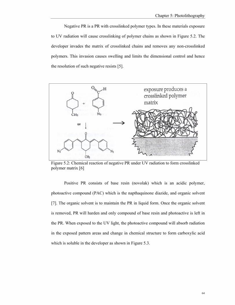
Chapter 5: Photolithography
64
Negative PR is a PR with crosslinked polymer types. In these materials exposure
to UV radiation will cause crosslinking of polymer chains as shown in Figure 5.2. The
developer invades the matrix of crosslinked chains and removes any non-crosslinked
polymers. This invasion causes swelling and limits the dimensional control and hence
the resolution of such negative resists [5].
Figure 5.2: Chemical reaction of negative PR under UV radiation to form crosslinked polymer matrix [6]
Positive PR consists of base resin (novolak) which is an acidic polymer,
photoactive compound (PAC) which is the napthaquinone diazide, and organic solvent
[7]. The organic solvent is to maintain the PR in liquid form. Once the organic solvent
is removed, PR will harden and only compound of base resin and photoactive is left in
the PR. When exposed to the UV light, the photoactive compound will absorb radiation
in the exposed pattern areas and change in chemical structure to form carboxylic acid
which is soluble in the developer as shown in Figure 5.3.

Chapter 5: Photolithography
65
Figure 5.3: Reaction of PAC prior to the exposure of the UV light [9].
The absorption of the UV radiation causes the nitrogen molecule (N2) to be free
from the carbon ring, leaving behind a highly reactive carbon site. The carbon that bond
to the oxygen atom will move out from the carbon rings to proceed to a more stable
structure which is called ketene. This process is known as a Wolff rearrangement [8].
With the presence of water, the double bond of the external carbon is replaced with the
single bond and an OH group creating a final product call carboxylic acid.
When the PR is in contact with the base solution, the PAC that was not exposed
to the UV radiation will not dissolve in the PR developer (base solution). On the other
hand, carboxylic acid which readily reacts with and dissolves in PR developer will
breakdown into water-soluble amines such as aniline and salts of K (or Na, depending
on the developer) [8]. The dissolution occurs rapidly for two reasons. The first is the
carboxylic acid mixture rapidly taking up water. Second, the nitrogen released in the
reaction will foam the resist, further assisting the dissolution [8].
5.2.2 PHOTOLITHOGRAPHY EXPOSURE METHOD
There are mainly three types of UV exposure method in photolithography
process. They are contact printing, proximity printing, and projection printing. Figure
5.4 reveals the basic structural difference of the methods by different mask alignment
systems. Contact printing is the simplest and most common method in photolithography
process as shown in Figure 5.4(a). In contact printing the photo-mask is held in the

Chapter 5: Photolithography
66
direction where the chrome pattern is facing down and brought into intimate contact
with the PR cover wafer. The exposure of the UV light will copy the pattern of the
photo-mask to the PR in the ratio of 1:1. This capability of high resolution printing with
inexpensive equipment is the primary advantage of contact printing. The resolution of
contact printing is determined by mask dimensions and diffraction at mask edges.
Theoretically, submicron patterns can be produced by using contact printing but to
create a submicron mask will be prohibitively expensive. With contact printing method,
there does not exist any space between mask and PR thus, minimizing the effect of
diffraction [8-10]. The disadvantage of contact printing would be the high chances of
scratching on the mask surface. Permanent damage might appear on the mask surface
due to any particle scratch on the PR surface when the mask contact with the PR under
certain pressure.
(a) (b) (c) Figure 5.4: Various UV exposure methods used in photolithography process
Proximity printing is a modification of contact printing to avoid damage caused
by contact printing as shown in Figure 5.4(b). In proximity printing, the mask is
separated from the PR layer at 10 to 50μm [7]. Although it solves the mask damage

Chapter 5: Photolithography
67
problem, the resolution also drops due to the diffraction effect. Light passing by the
edges of an opaque mask feature will form fringes and penetrates into the shadow
region. This effect can be explained by Fresnel diffraction, or more specifically,
Huygen’s wavelets [8]. The Fresnel diffraction limits the resolution to a minimum of
about 5μm.
Projection printing is designed to have a high resolution of contact printing
without the defect in contact printing as shown in Figure 5.4(c). In projection printing,
the aligner has been developed to project an image of the mask patterns onto a resist-
coated wafer many centimeters away from the mask. The light that passes through the
mask will be diffracted to a large angle. An objective lens called projector is placed in
between the mask and the wafer to reimage the pattern onto the PR. For the projector to
be able to collect the diffracted light, the acceptance angle (2α) of the projector must be
larger than the diffraction angle of the light. The acceptance angle of the projector is
related to the system numerical aperture, NA by the following equation:
αsinnNA = (5.1)
where α is one-half the angle of acceptance of the projector and n is the refractive index
of the media between the projector and the wafer. Normally the exposure is done in air
where n = 1.0. Typical values for NA range from 0.16 to 0.8 [8].
The resolution limitation of the projection printing is referred to as Rayleigh’s
criteria, Wmin and is given by
NAkW λ
≈min (5.2)
where k is a constant that again depends on the ability of the PR to distinguish between
small changes in intensity (typically k is of order 0.75) and λ is the wavelength of the
UV light source.

Chapter 5: Photolithography
68
The reduction of the depth of focus (DOF), σ is the technical price that has to be
paid by projection printing to gain the high resolution with fewer defects. DOF is the
distance where the wafer can be moved while maintaining the projection image in focus
[8]. The DOF can be calculated by equation 5.3
2NAλσ = (5.3)
The degradation in DOF has made this approach to be difficult. In addition,
there are also issues such as wafer flatness, resist thickness, and stage level to overcome.
Thus a tradeoff between resolution and DOF limitations is necessary.
5.3 PHOTOLITHOGRAPHY PROCESS METHODOLOGY
In order to ensure minimal contamination of samples, both deposition and
photolithography are carried out in a controlled environment. The photolithography
process in University of Malaya (UM) is run in a class 10k clean room under yellow
light condition. The clean room is a necessary pre-requisite because dust particles in the
air can settle on the wafer or photomask and cause defects. The dust particles that lay on
the mask will behave as opaque patterns on the mask while the dust particles that lay on
the wafer surface might create permanent scratch or damage to the mask. Class 10k
(10,000) clean room means the clean room has maximum dust count of 10k particles/ft3
with particles diameters of 0.5μm or larger [7].
The 10k clean room is further divided into two sections. The larger section
houses fabrication instruments like Flame Hydrolysis Deposition (FHD), furnace,
Inductive Coupled Plasma (ICP), and Direc-Current (DC) sputtering system. Our
photolithography process is run in a separate room called yellow room. The yellow
color is the result of utilizing the UV filter of the fluorescent lamp. The Yellow room is
needed due to the application of PR in photolithography process. PR is photosensitive to

Chapter 5: Photolithography
69
light from wavelength 310 - 440nm and completely transparent after wavelength 475nm.
Thus yellow light which contain wavelength from 570 – 580nm is use in
photolithography room.
5.3.1 PR COATING
Before starting the photolithography process, the wafer must be cleaned
(Appendix B provides the wafer cleaning procedure practiced by our lab) as
photolithography process require highly clean environment in order to work. In UM,
positive photoresist (AZ1518 or AZ1512) is applied on the top of the wafer by spin
coating method. Spin coating is one of the simplest and most common techniques of
applying thin PR onto wafers. PR coating is carried out by dispersing of the PR onto the
wafer, typically in the form of non-uniform stream by using pipette. The pipette is held
as near as possible to the wafer surface to reduce the chances of trapping air or dust
during the process. Air bubbles or dust trapped in the PR will cause defects in the
photolithography process. After the PR was dispensed onto the wafer, the wafer is
accelerated to the required speed slowly.
The rotation of the wafer will cause the PR to spread over the surface of wafer.
The increase of the rotation speed will then create an aggressive fluid expulsion from
the wafer surface. More and more PR on the top layer will be applied while the wafer
below rotates faster and faster. When the wafer reached the required speed, the PR is
thin enough that the viscous shear drag exactly balances the rotational accelerations. At
the constant speed, PR will experience the thinning process. The PR thinning is quite
uniform throughout this stage. This process becomes progressively slow as the coating
thickness is reduced. This phenomenon can be observed as the interference colors ring
stop expanding outward. When the PR become thin enough, solvent evaporation will
dominated the coating thinning behavior. At this point onwards, the PR will slowly

Chapter 5: Photolithography
70
transform into “gels” as the solvents are removed. The wafer will then decelerate and
move to next process.
5.3.2 PREBAKE
The evaporation of solvent in the spin coating process involves only the top
surface layer. Further removal of the solvent is done by baking the wafer on a hotplate.
This process is prebaking, where the wafer is heated at temperatures not exceeding
100°C for less than 2 minutes. The baking process will remove most of the solvent.
Only a low percentage of the solvent remains in the dried resist due to the high boiling
point of solvent (>134°C). The residual solvent will influence the dissolution rate of
exposed resist. If the prebake temperature is increased above 100°C, the light sensitive
naphthoquinone diazide (PAC) is thermally decomposed and lithographic performance
is degraded. Thus, temperature and time are quite critical in prebaking.
5.3.3 MASK ALIGNER
Running UV exposure, the wafer is placed at the substrate holder and the
photomask is held above the wafer. A contact aligner is used in UM for UV exposure
purposes. The wafer on the substrate holder will then move up slowly until the wafer
and the photomask is nearly in contact with each other. Contact between wafer and
photomask can be observed when there are fringes appearing on at the mask. The
position of the substrate holder is adjusted so that the wafer is placed at the center of the
photomask. After that, the wafer is moved towards the photomask until they are in
contact. Vacuum is then applied to remove the air trapped in between wafer and
photomask. Once this is achieved, we can observe that fringes are distributed all over
the wafer. The vacuum pressure is increased slowly until the fringes seem to be static
throughout the whole wafer.

Chapter 5: Photolithography
71
Once the wafer is properly positioned, it is UV exposed according to the preset
exposure dose. The UV light is generated from a mercury arc lamp source which emits
radiation wavelength from 275nm to 650nm. It has a very high radiant intensity in the
350 – 450nm wavelength range especially in 365nm (i-line), 405nm (h-line), and
436nm (g-line).
5.3.4 DEVELOPMENT
Those PR which expose to UV will become carboxylic acid and this can be
diluted in a PR developer. The developer used in UM is AZ 726 MIF, which is a metal
ion free aqueous alkaline solution of 2.38% tetra-methyl-ammonium-hydroxide with
surfactant to provide fast and uniform build-up of the puddle. The developing process is
run under room temperature for 20 to 50 seconds depends on the PR thickness. After
development, the wafer will be rinsed with DI (De-Ionized) water and dried with
nitrogen gas.
5.3.5 POSTBAKE
The developed wafer will need to be baked again before being sent for Cr wet
etching. This post baking process will further stabilize the PR, improving adhesion
during wet etching. The wet etching process must be carried out within 2 hours of post
baking to ensure good quality results.

Chapter 5: Photolithography
72
5.4 EXPERIMENTAL RESULTS AND DISCUSSIONS
5.4.1 PHOTORESIST (PR) COATING
In PR coating, PR dispending method and timing plays an important role to
produce a uniform PR layer. In this study, the PR was dispensed manually by using a
pipette onto the wafer in various stages. The first study is the static dispensing
technique (SDT) where the PR was dispensed onto the wafer surface before the wafer is
spin. This is followed by second study is the dynamic dispensing technique (DDT)
where the PR was dispensed onto the wafer surface while the wafer is spinning. In the
first DDT, the PR was dispensed while the wafer is being accelerated towards
maximum speed while in second DDT experiment, the PR was dispensed during the
wafer is in maximum spin speed.
After patterning on the PR layer, the PR thickness was measure using surface
profiler (Tencor Alpha Step 2000). For higher accuracy, thicknesses were measured at
various points across the wafer diameter. Figure 5.5 shows the PR thickness of the
patterned channel at different spin speeds for SDT and both DDTs. As shown in the
figure, the thickness of the PR coating reduces as the spin coater speed is increased.
This thinning behavior is due to the viscous fluid forces that spread the PR towards the
edge of the substrate. Both DDTs show a lower thickness compared to SDT. The second
DDT for instance shows a thickness reduction of 0.2 μm in comparison to the SDT at
the spinning speeds of above 8000 rpm. When comparing both DDTs, the second
technique shows a better thinning behavior especially for spinning speeds above 4000
rpm. At lower spinning speeds, the PR thinning behavior is only slightly improved due
to the small differences between the maximum spinning speed and acceleration speed.
The centrifugal forces that were created in both cases are also similar. Thus, thickness
differences between SDT and the two DDTs at lower speeds are seen to vary at around
tens of nanometers. When the maximum spinning speed is set higher, thickness

Chapter 5: Photolithography
73
differences (due to the increasing centrifugal force) become more significant. At 9000
rpm, thicknesses different around (0.10±0.01) μm was observed.
Figure 5.5: PR thickness (μm) versus spin coating speed (rpm) for SDT, 1st DDT and 2nd DDT
Figure 5.6 shows the circular non-uniformity of the PR thickness measured from
the center of the substrate to its edge. As shown, the average non-uniformity of the PR
thickness is reduced from SDT (average= (0.28±0.01) μm) to 1st DDT (average=
(0.21±0.01) μm) and 2nd DDT (average= (0.14±0.01) μm). However, the variations in
the non-uniformity have increased from SDT to 1st DDT and 2nd DDT. This means that,
although the PR uniformity has averagely increased from SDT to the 2nd DDT, the
uniformity control is more difficult. In SDT, there is a delay between the PR dispensing
on the substrate and the spin cycle. The PR, when dispensed at the center of the
substrate will evaporate during this delay causing its distribution to be unevenly thicker
at the center. Using DDT on the other hand, the PR is spread out once it touches the
substrate surface. This application of PR without spin delay causes wider spreading of
the chemical layer and reduced central clumping. The PR layer uniformity and
distribution is thus, improved for DDT in comparison to SDT.

Chapter 5: Photolithography
74
Figure 5.6: Illustration of PR thickness non-uniformity with various PR dispensing techniques
Since the increment of spinning speed increases the evaporation rate and
centrifugal force, the PR undergoes the highest evaporation rate and centrifugal force in
the 2nd DDT followed by the 1st DDT and SDT. Because of the high evaporation rate in
both DDTs, the PR dispensing rate will affect the PR uniformity on the wafer. The PR
dispensing rate should be fast and consistent to achieve a better uniformity control. If
the PR dispensing rate is too slow, more than one layer of PR will be formed on the
wafer surface.
Table 5.1 shows the amount of PR used for different dispensing techniques. As
shown, the minimum PR quantity required for the coating process is approximately
3.00ml in SDT. In both DDTs, the PR quantity has reduced to 0.25ml, which is about
8.33% of the quantity required by SDT. The excess quantities of PR required in SDT
are lost during the spin stage [11]. This means that the DDT methods are more
economical and environmentally friendly. Figure 5.7 shows the PR with spin speed of
6000rpm and various amount of PR. Notice from Figure 5.7 that the resultant PR
thickness is independent of the amount of PR applied. As such, less amount of PR can
be used without affecting the PR thickness.

Chapter 5: Photolithography
75
Table 5.1: PR usage in SDT, 1st DDT and 2nd DDT
PR Usage (±0.05) ml
3.00 2.00 1.00 0.50 0.25 0.20
Static Dispensing √ X X X X X
1st Dynamic Dispensing √ √ √ √ √ X
2nd Dynamic Dispensing √ √ √ √ √ X
* √ = The PR amount used is sufficient for whole surface coverage of the substrate. X = The PR amount used failed to cover the whole surface of the substrate.
Figure 5.7: Thickness variation of PR applied using the 1st DDT approach

Chapter 5: Photolithography
76
5.4.2 PREBAKE
As mentioned earlier, temperature and prebaking duration are two important
parameters that will determine solvent evaporation percentage and also the sensitivity of
the photoactive compound (PAC). Figure 5.8 shows the graph of PR thickness
dependence on various prebake temperatures. We notice that the thickness of the PR is
reduced when the wafer is prebaked at higher temperatures. For temperatures above or
equal to 140oC, the developing process became unsuccessful. In addition, prebaking at
high temperatures will leave behind residual PR that could not be removed from the
chromium surface. This is shown in the image in Figure 5.9. This will subsequently
cause contamination in the glass etching process. As such, temperatures within 60oC to
100oC are likely to produce the best results, along with shorter developing times (20s-
50s).
Figure 5.8: PR thickness dependence on various prebake temperatures

Chapter 5: Photolithography
77
Figure 5.9: PR residual that fail to remove from wafer after PR removal process
A comparison is made between prebake temperatures of 60oC, 80oC, and 100oC
for different baking period as shown in Figure 5.10. PR thickness for 60oC and 80oC
still show a decrease even after 5 minutes of prebaking on a hotplate while for the case
of 100oC, the thickness remains constant. Therefore, in light of these findings, we could
conclude that 100oC is the most suitable prebake condition..
Figure 5.11 shows the depletion of the PR layer while baking under 100oC. A
critical drop of PR thickness can be observed at during first minute of the prebake. The
depletion of the PR layer seems to be insignificant after 2 minutes when most of the
solvent is removed. Hence, prebake temperature is set at 100oC for 2 minutes since no
significant change to the PR thickness after 2 minutes baking. 2 minutes is chosen
because a longer exposure period will reduce the sensitivity of the PAC, and this would
result in the reduction of the pattern resolution.

Chapter 5: Photolithography
78
Figure 5.10: PR thickness for prebaking temperature of 60oC, 80oC, and 100oC, for various prebake duration
Figure 5.11: Change of PR thickness with various prebaking duration

Chapter 5: Photolithography
79
5.4.3 UV EXPOSURE
In UV exposure, the contact method employed will have a significant impact on
the resultant transferred pattern. For this study, three different contact methods were
investigated – soft contact, hard contact, and vacuum contact. Figure 5.12 depicts the
resulting PR pattern using the respective approaches. Figure 5.12(a) shows the result for
soft contact printing where the resolution is lower compared to those presented in
5.12(b) and 5.12(c). The branching part was under exposed and subsequently causes
incomplete PR development. Figures 5.12(b) & (c) show comparatively better results on
PR patterning which are done under hard contact and vacuum contact. The hard contact
approach is quite consistent in generating repeatable results but it susceptible to mask
damage, creating permanent defects. Vacuum contact is also able to produce good PR
patterns, but the results repeatability is low. The success of the vacuum technique is
highly dependent on the uniformity of the PR layer using the vacuum technique on a
non-uniform PR layer will result in pattern with varying resolution, as depicted in
Figure 5.12(c) and 5.12(d).
The resolution and the CD of the patterning process can be measured using the
error analysis scale printed on the AWG mask used as shown in Figure 5.13. The
numbers under the pattern are all in micron unit. The scale in Figure 5.13(a) is used to
measure the CD error while that scale in Figure 5.13(b) is used to measure the
resolution limits of the patterning process. For a 7μm width pattern, the contact method
will display a typical CD error of ±0.4μm. However, contact plays an important role in
producing a high resolution pattern. When the contact between the mask and the wafer
is not close enough, the separation will cause Fresnel diffraction, and hence reduce the
resolution of the transferred pattern. Figure 5.14 depicts samples under different hard
contact pressure. Sample (a) under 0.2MPa pressure produced better resolution (1.2μm)
while sample (b) under 0.16MPa pressure displayed lower resolution (1.8μm).

Chapter 5: Photolithography
80
(a) (b)
(c) (d) Figure 5.12: PR pattern obtained with (a) soft contact, (b) hard contact, and (c) and (d) for vacuum contact
(a)
(b)
Figure 5.13: Error analysis scale on AWG photomask, (a) for CD error measurement while (b) for resolution limit measurement
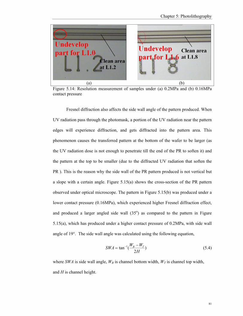
Chapter 5: Photolithography
81
(a) (b) Figure 5.14: Resolution measurement of samples under (a) 0.2MPa and (b) 0.16MPa contact pressure
Fresnel diffraction also affects the side wall angle of the pattern produced. When
UV radiation pass through the photomask, a portion of the UV radiation near the pattern
edges will experience diffraction, and gets diffracted into the pattern area. This
phenomenon causes the transferred pattern at the bottom of the wafer to be larger (as
the UV radiation dose is not enough to penetrate till the end of the PR to soften it) and
the pattern at the top to be smaller (due to the diffracted UV radiation that soften the
PR ). This is the reason why the side wall of the PR pattern produced is not vertical but
a slope with a certain angle. Figure 5.15(a) shows the cross-section of the PR pattern
observed under optical microscope. The pattern in Figure 5.15(b) was produced under a
lower contact pressure (0.16MPa), which experienced higher Fresnel diffraction effect,
and produced a larger angled side wall (35o) as compared to the pattern in Figure
5.15(a), which has produced under a higher contact pressure of 0.2MPa, with side wall
angle of 19°. The side wall angle was calculated using the following equation,
)2
(tan 1
HWWSWA TB −
= − (5.4)
where SWA is side wall angle, WB is channel bottom width, WT is channel top width,
and H is channel height.

Chapter 5: Photolithography
82
(a) (b) Figure 5.15: Cross-section of PR pattern produced under (a) 0.2MPa and (b) 0.16MPa contact pressure
The suitability of the contact method and the pressure applied can be observed
from the fringe patterns when the photomask is in contact with the PR coated wafer.
The fringe pattern shows the contact condition between the wafer and photomask. The
bigger the size of the fringes means the better the contact condition, and therefore,
better the pattern will be produced. The fringes should also be uniform throughout the
whole wafer. Figure 5.16 shows the fringe pattern when the photomask is in contact
with the PR coated wafer.
Figure 5.16: Fringe pattern when the photomask is in contact with the PR coated wafer

Chapter 5: Photolithography
83
In UV exposure, the exposure dosage and development time are dependent on
each other, and both also depend on the prebake condition [12]. Since the prebake
condition is fixed at the previous stage, here we only consider exposure dosage and
developing time. In this study, the development time is best in 20 seconds to 30 seconds,
so any exposure dosage that need more than 30 seconds developing time will not be
considered. PR is developed for 30 seconds after expose with different dosage and the
results are observed under objective microscope. The dosages increase slowly until all
the PR residual successful to be removed within 30 seconds.
Figure 5.17(a) & (b) show the PR pattern that still contain PR residual which is
not being developed all in between the branches. Figure 5.17(c) shows the result of the
successful develop PR pattern while Figure 5.17(d) shows the results of the PR pattern
which exposed to over expose dosage. Figure 5.18 shows the optimized UV exposure
dosage for different thickness of PR layer. It shows a non-linear increase of exposure
dosage needed for different PR layer thickness.

Chapter 5: Photolithography
84
(a) (b)
(c) (d) Figure 5.17: PR pattern with different exposure dosage. (a) 1860 mJ/cm2, (b) 1890 mJ/cm2, (c) 1920 mJ/cm2, and (d) 2100 mJ/cm2
Figure 5.18: Different exposure dosages for varying PR thickness

Chapter 5: Photolithography
85
5.4.4 POSTBAKE
The postbake process is recommended to improve the PR adhesion to the Cr
etchant. Figure 5.19 shows the independence of PR thickness on the postbake period by
using a hotplate set at 100°C. The PR thickness does not show any significant changes
as most of the solvent in the PR was already removed during prebake process. At the
same time, the Cr wet etching results which were done under postbake condition for 2
minutes and without postbake was observed under optical microscope. Figure 5.20
shows the overlapping image of the two results. The darker colour part is the etched Cr
pattern without postbake, while the brighter colour is the etched Cr pattern with 2
minutes of postbake. Both results do not show any significant difference in CD but the
pattern without postbake shows sharper edges at the corner.
Figure 5.19: Resulting PR thickness for different postbake period
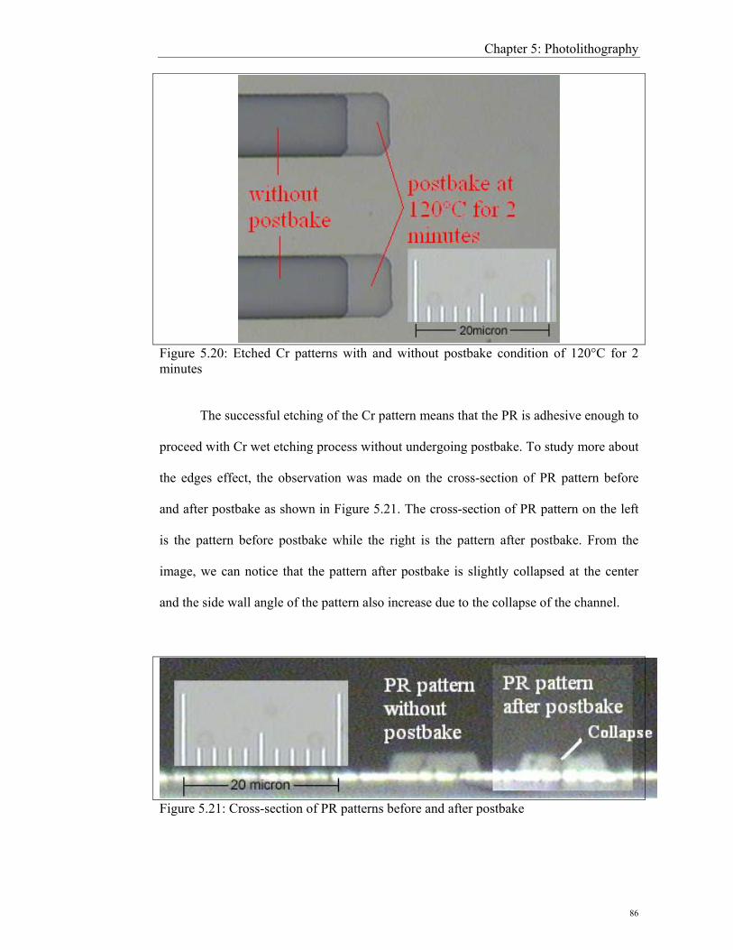
Chapter 5: Photolithography
86
Figure 5.20: Etched Cr patterns with and without postbake condition of 120°C for 2 minutes
The successful etching of the Cr pattern means that the PR is adhesive enough to
proceed with Cr wet etching process without undergoing postbake. To study more about
the edges effect, the observation was made on the cross-section of PR pattern before
and after postbake as shown in Figure 5.21. The cross-section of PR pattern on the left
is the pattern before postbake while the right is the pattern after postbake. From the
image, we can notice that the pattern after postbake is slightly collapsed at the center
and the side wall angle of the pattern also increase due to the collapse of the channel.
Figure 5.21: Cross-section of PR patterns before and after postbake

Chapter 5: Photolithography
87
5.5 SUMMARY
In this chapter, the optimization of the photolithography process has been done
in every stage starting from PR coating to postbake. In PR coating, three different
dispensing method have been tested to obtain the best coating quality, and they were
SDT, 1st DDT, and 2nd DDT. Both DDT methods show improvement in PR layer
thinning, uniformity, and less chemical usage. However, DDT methods have lower
repeatability and higher percentage of creating defects during the coating process.
Prebake is critical as it will affect the UV exposure and developing processes.
Prebake temperature and period were optimized to remove most of the solvent in PR
while maintaining PAC sensitivity. Contact methods and UV exposure dosage were
presented in this chapter as well. It was found that by using the correct combination of
contact method and UV exposure, PR pattern of CD error less than 6% of the pattern
width, and side wall angle of less than 20o can be achieved.
The final section discussed the effect of postbake to the resulting PR pattern and
wet etching process. Although in most processes postbake is important to increase the
adhesiveness of the PR in wet etching process, however this step does not seems to be
necessary to our process. The postbake also causes the PR pattern to collapse at certain
areas and hence increase the CD error.

Chapter 5: Photolithography
88
REFERENCES
[1] Darling, R. B. Micro Fabrication – Photolithography. Retrieved October 29,
2007, from University of Washington website:
http://www.ee.washington.edu/research/microtech/cam/PROCESSES/PDF%20F
ILES/Photolithography.pdf
[2] Snyder, I. (1996). Color printing in the nineteenth century. Retrieved January 24,
2008 from University of Delaware Library website:
http://www.lib.udel.edu/ud/spec/exhibits/color/lithogr.htm
[3] Bruning, J. H. (1997). Optical Lithography - Thirty years and three orders of
magnitude (The evolution of optical lithography tolls). SPIE, 3051, 14-27.
[4] Edgar, T. F., Butler, S. W., Campbel, W. J., Pfeiffer, C., Bode, C., Hwang, S. B.
et al. (2000). Automatic Control in Microelectronics Manufacturing: Practices,
Challenges, and Possibilities. Automatica, 36 (11), 1567-1603.
[5] Smith, H. I. Submicron and Nanometer Structures Technology. Retrieved from
Massachusetts Institute of Technology Lecturer Note.
[6] Wilson, C.G., Dammel, R.A., & Reiser, A. (1997). Photoresist Material: A
Historical Perspective. SPIE, 3051, 28-41.
[7] May, G. S., & Spanos, C. J. (2006). Fundamentals of Semiconductor
Manufacturing and Process Control. Hoboken, New Jersey: John Wiley & Sons.
[8] Campbell, S. A. (2001). The Science and Engineering of Microelectronic
Fabrication (2nd ed.). New York: Oxford University Press.
[9] Franssila, S. (2004). Introduction to Microfabrication. Chichester, England: John
Wiley & Sons.
[10] Thompson, B. J. (2007). Microlithography - Science and Technology (2nd ed.).
New York: Taylor & Francis Group.
[11] Derksen, J., Han, S.J., & Chun, J.H. (2004). Extrusion Spin Coating: An
Efficient and Deterministic Photoresist Coating Method in Microlithography.
Semiconductor Manufacturing, 17 (1), 245-248.
[12] Hiroshi, M. & Mehran, M. (1995). High-Aspect-Ratio Photolithography for
MEMS Applications. Journal of Microelectronical Systems, 4 (4), 220-229.

Chapter 6: Wet Etching
89
CHAPTER 6
WET ETCHING
6.1 INTRODUCTION
Wet etching is a conventional, purely chemical, etching process where the wafer
is immersed in a solution that reacts with an earlier ultra-violet (UV) exposed thin film
to form soluble by-products [1]. Unfortunately, the limitations of wet etching due to the
isotropic etching profile, poor process control, large volumes of chemical waste,
unsuitability for small features, and excessive particle contamination, have reduced its
popularity [1, 2]. However, compared to dry or plasma etching, wet etching is a much
cheaper option as it does not rely on expensive equipment, more suitable for mass
production, highly selective and often does not damage the substrate. As a result, the
technique continues to be used for most semiconductor etching processes that are
“noncritical”. Tank (or bath), spray tool, and single-wafer processor are three general
methods for performing wet etching process.
6.2 OVERVIEW
Isotropic etching is a non-directional removal of material from a substrate via a
chemical process using an etchant substance. Most of the wet etching process
performed as an isotropic etching due to the random movement of the liquid molecular.
The isotropic etching nature of wet etching will create undercut issues. Undercut is the
lateral extent of etch under a photoresist (PR) mask as shown in Figure 6.1.
There are two ways to describing undercut. The first is by considering the
undercut distance per side. It can be calculated by dividing the difference between PR
patterned line and the etch chromium (Cr) pattern by 2. As shown in Figure 6.1, the side
wall of the Cr pattern may not be vertical. Thus the undercut value is based on how the

Chapter 6: Wet Etching
90
Cr pattern is measured. The second way is to quote the etch rate anisotropy. Anisotropy
is given by
V
L
RRA −= 1 (6.1)
where RL and RV are lateral and vertical etch rates. Thus for perfectly anisotropic (A =
1), lateral etch rate is zero while A = 0 for isotropic etching with same lateral and
vertical etch rate [1].
Figure 6.1: Schematics of undercutting caused by the isotropic nature of wet etching
For Cr wet etching, Cr etchant (Cr 7S) is used to remove the unwanted part of
the Cr which are not covered by PR. Cr etchant include composition of perchloric acid
(HClO4), ceric ammonium nitrate ((NH4)2Ce(NO3)6), and water (H2O) [3]. Perchloric
acid is a very strong acid and therefore almost completely dissociated in aqueous
solution (pKs < -8), and serves to chemically stabilize the ceric ammonium nitrate.
Ceric ammonium nitrate itself is a very strong oxidizer. Equation (6.2) below shows the
chemical reaction in the Cr etching process by using Cr etchant Cr-7S:
5324336324 )()(3)()()(3 NOCeNHNOCrCrNOCeNH +→+ (6.2)
From the equation, notice that cerium oxidation state is reduced from IV to III,
whereas the chromium oxidation state increases from II to III [4].

Chapter 6: Wet Etching
91
6.3 Cr WET ETCHING PROCESS METHODOLOGY
In this study, Cr was etched by using different wet etching methods to study the
advantages and disadvantages of each method. The methods that were used include:
a) Static immersion - wafer is immersed into beaker with 100ml of Cr etchant and
was left static until the etching process is done.
b) Flipping – wafer is immersed into beaker with 100ml of Cr etchant and the
wafer is flipped up and down until the etching process is done.
c) Spin stirrer – wafer is immersed into beaker with 100ml of Cr etchant and stirred
using magnetic bar until the etching process is done.
d) Ultrasonic – wafer is immersed into beaker with 100ml of Cr etchant and put
into an ultrasonic bath until the etching process is done.
e) Heating – wafer is immersed into beaker with 100ml of Cr etchant that was
already heated up to a predetermined temperature using a hotplate until the
etching process is done.
When the etching process starts, it can be observed that the wafer surface will
slowly darken. This is due to the chromium nitrates that were produced during the
etching forming a dark film on the chromium surface. Chromium nitrate is soluble and
it will dissolve in the etchant itself [4]. The etching process is completed when the
wafer surface reverts back into its shiny surface feature. The wafer will be left in the
etchant for an additional 5 seconds to make sure that all unwanted Cr are removed. The
etched wafer will then be rinsed using DI water for 5 minutes to remove residual
chemicals. Acetone is then used to remove the PR pattern on the wafer. The wafer will
then undergo a cleaning process, as described in Appendix B. The cleaned wafer will
then be sent for glass etching.

Chapter 6: Wet Etching
92
6.4 EXPERIMENTAL RESULTS AND DISCUSSIONS
a) Static immersion
In static immersion wet etching, wafer was etched using Cr etchant in beaker
without any disturbance at room temperature. From observation, the etching processes
normally end faster at the edge of the wafer then only slowly proceeding towards the
center. The difference of the etching period between edge and core is caused by the
non-uniformity of the Cr thin film layer. Besides that, wafer edge which has higher
exposure area (wafer top area and side area) to the Cr etchant also increases the Cr
etching rate at the edge. Figure 6.2 shows the Cr etching time needed for the edge and
the center of the wafer with different Cr deposition time (*Cr deposition time is
proportional to Cr thin film thickness).
Figure 6.2: Cr wet etching time for different Cr deposition periods
Figure 6.3 shows the difference in etching time between the edges and center
(EC period). The difference in etching time between various locations on the wafer is a
critical issue that needs to be catered for. Uniform etching in this case could not be
achieved as some of the regions will etch quicker resulting in over-etching [5]. Over-

Chapter 6: Wet Etching
93
etching will cause undercutting in isotropic etching (wet etching). In more serious cases,
complete loss of pattern due to undercut can take place, reducing the yield of the
patterning process [2].
Figure 6.3: Difference in etching time between the edge and center of a wafer in various chromium deposition times
Figure 6.4 shows the critical dimension (CD) error of the AWG Cr pattern. CD
error is the difference of the transfer pattern width to the original pattern width. Positive
value means the dimension of the transfer pattern is smaller than the original pattern
while negative value means the opposite. Due to the increase of the EC period for
thicker Cr layer, and hence CD error also increase as the Cr deposition time increase.
CD errors for samples that deposited Cr for 8 and 10 minutes are out of the error
measuring scale which is larger than 2.4μm are not included in the graph.
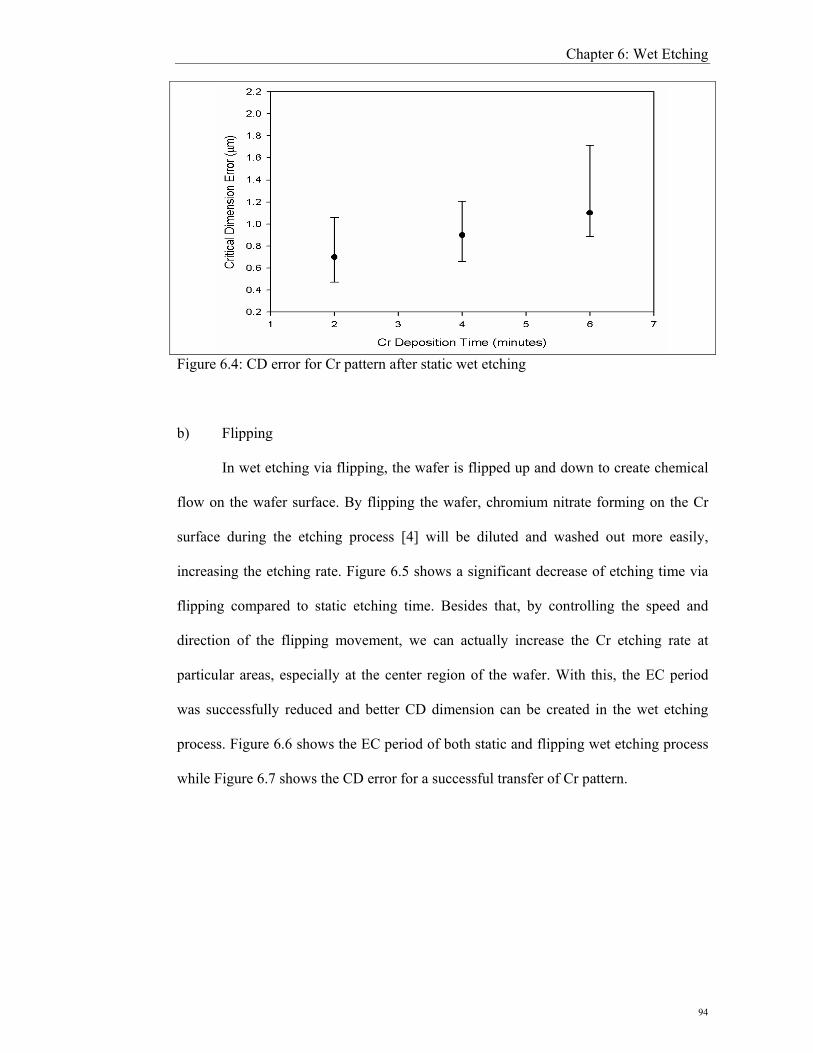
Chapter 6: Wet Etching
94
Figure 6.4: CD error for Cr pattern after static wet etching
b) Flipping
In wet etching via flipping, the wafer is flipped up and down to create chemical
flow on the wafer surface. By flipping the wafer, chromium nitrate forming on the Cr
surface during the etching process [4] will be diluted and washed out more easily,
increasing the etching rate. Figure 6.5 shows a significant decrease of etching time via
flipping compared to static etching time. Besides that, by controlling the speed and
direction of the flipping movement, we can actually increase the Cr etching rate at
particular areas, especially at the center region of the wafer. With this, the EC period
was successfully reduced and better CD dimension can be created in the wet etching
process. Figure 6.6 shows the EC period of both static and flipping wet etching process
while Figure 6.7 shows the CD error for a successful transfer of Cr pattern.

Chapter 6: Wet Etching
95
Figure 6.5: Etching time needed for flipping and static wet etching over various Cr deposition duration
Figure 6.6: The significant reduction of EC period for flipping etching as compared to static etching

Chapter 6: Wet Etching
96
Figure 6.7: CD error for different Cr deposition times
c) Spin stirrer
This technique failed to produce the desired results. The turbulence caused by
the technique resulted in a significantly higher etching rate at the edge of the samples to
that at the centre. This causes the outer patterns to be over-etched, and eventually
destroyed at the end of the etching process.
d) Ultrasonic
In ultrasonic etching, the etching beaker was put in the center of an ultrasonic
chamber filled with ultrasound conducting fluid. This method is to utilize the energy
carried by the vibration of ultrasound standing wave to increase the chemical reaction
[6]. From Figure 6.8, we can observe that the Cr etching rate is slightly higher
compared to the static etching method, due to the higher vibration energy transferred
from the ultrasound. In terms of CD error, this technique is comparable to static etching.
Figure 6.9 shows the CD errors for different Cr layer thickness.

Chapter 6: Wet Etching
97
Figure 6.8: Cr etching time by using static and ultrasonic etching method
Figure 6.9: CD error for Cr pattern with ultrasonic etching

Chapter 6: Wet Etching
98
e) Heating
In the heating wet etching process, the Cr etchant is heated to study the effect of
the etching temperature have on the chemical reaction. The process was carried on in
the fume hood as Cr etchant vapour is poisonous. Heating up the Cr etchant will provide
additional energy to the etchant molecules, which will then increase the chemical
reaction between the etchant and Cr. Figure 6.10 shows the dependence of the etching
rate on the temperature.
Although the etching rate was increase as the chemical temperature increases, it
does not seem to improve Cr pattern CD. The etching results look fine for low Cr
thickness (deposition period at 6 minutes and below) but over etch effect still appears
for high Cr thickness (deposition period at 8 minutes and above).
Figure 6.10: Cr etching rate at different temperatures

Chapter 6: Wet Etching
99
6.5 SUMMARY
In this chapter, various wet etching methods have been investigated to improve
the Cr pattern quality in the wet etching process. The flipping approach produced the
best results where the resulting Cr patterns displace the lowest CD error. Static and
ultrasonic etching produced almost similar results whereas heating increases the etching
rate, but does not produce a quality pattern as the chemical was too reactive. The spin
stirrer with hotplate technique was found to be unsuitable as the Cr patterns at the edge
of the samples were completely etched due to the large difference in etching rate caused
by the temperature gradient.
In this chapter we also observed that although a higher etching rate will shorten
the process duration, it does not lead itself to producing quality etching patterns. As
such, a compromise must be reached between etch rate and pattern quality. Finally,
from the results obtained, we could conclude that the flipping method is most suitable
for our process. A summary of the results is provided in table 6.1.
Table 6.1: Summary of different Cr wet etching techniques for 6 minutes Cr deposition period
Technique CD Error (±0.2μm) Pattern Yield (%) Cr Etch Rate (±5nm/minute)
Static immersion 1.0 - 2.0 100 40
Flipping 0.4 – 0.8 100 130
Spin Stirrer > 2.4 10 50
Ultrasonic 1.8 – 2.4 100 45
Heating * CD error and pattern yield are totally depend on technique used above. Heating only improve the etching rate with 0.1nm/minute for every Degree Celsius of temperature increase.
Chapter 6: Wet Etching
100
REFERENCES
[1] Campbell, S.A. (2001). The Science and Engineering of Microelectronic
Fabrication (2nd ed.). New York: Oxford University Press.
[2] Franssila, S. (2004). Introduction to Microfabrication. Chichester, England: John
Wiley & Sons.
[3] MSDS (Material Safety Data Sheet) of Cr-7S from Cyantek Corporation.
Retrieved March 22, 2008, from http://www.cise.columbia.edu/clean/msds/CR-
7S.pdf
[4] Technical information of Cr etching from MicroChemicals. Retrieved March 22,
2008, from
http://www.microchemicals.com/technical_information/chromium_etching.pdf
[5] Peter, V.Z. (2000). Microchip Fabrication- A Practical Guide to Semiconductor
Processing (4th ed.). New York, US: The McGraw-Hill Companies, Inc.
[6] Crocker, M.J. (1998). Handbook of Acoustics. New York: J. Wiley.

Chapter 7: Conclusions & Future Work
101
CHAPTER 7
CONCLUSIONS & FUTURE WORK
7.1 CONCLUSIONS
During my master research, I have demonstrated the following
i) Characterization and optimization of the Chromium (Cr) thin film deposition
process by using Direct-Current (DC) planar magnetron sputtering deposition method.
Parameters like deposition period, DC power, argon (Ar) gas flow, substrate
temperature, and chamber pressure have been studied to understand the effects on the
thin film properties especially thickness, grain size and chemical stability. In this thesis,
discussion was concentrate in deposition period, DC power, and chamber pressure as
other parameters do not give any significant impact on those important parameters in
this thesis. Under the conditions of 0.8A DC current, 5sccm Ar flow rate, 30oC substrate
temperature, and 10mTorr process chamber pressure, the deposition process show a
linear increase in thickness when deposition period increase. The deposition rate is
43nm/minutes. The growth of the grain height from 3.5nm (for 2 minutes deposition) to
11.6nm (for 10 minutes deposition) when the Cr thickness is increase.
In DC current parameter study, the deposition rate is directly proportional to the
increase of DC current supply. The deposition rate shows increases of 52nm/minutes for
every ampere (A) of DC current supply. Besides the deposition rate, the change of the
deposition current do not shows any significant effect on the Cr thin film properties.
From these two parameters study, we notice that the chemical stability give a deep
impact in etching the thin film. The un-uniform etching rate at different area of the
wafer causes series over etching problem. This effect become more series when the Cr
thin film thickness increase until 60% of the Cr patterns are totally gone for etching Cr

Chapter 7: Conclusions & Future Work
102
film thickness around 500nm. However, this problem was improved in the study of
process pressure. By reducing the process pressure from 10mTorr to 6mTorr, the
different etching period in a same wafer was successfully reduced from ~200s to ~160s,
which is 20% improve from the original recipe. With this improvement, the Cr
patterning yield had improved from 40% to 100%.
ii) Photolithography process involved a series of processes from photoresist (PR)
spin coating till post baking. In PR spin coating, three different PR dispensing
techniques have been tested to study their advantages and reliability, which are the
conventional static dispensing technique (SDT), 1st dynamic dispensing technique (1st
DDT), and 2nd dynamic dispensing technique (2nd DDT). Three techniques show an
inversely proportional relation between coated PR thickness and spin coating speed.
However, there is a significant decrease in overall PR thickness from SDT to 1st DDT
and 2nd DDT. Besides that, PR uniformity also improved following the sequence above
from average 0.28μm to 0.21μm and to 0.14μm. Unfortunately, defects are easier to
create in 1st and 2nd DDT and the repeatability is also lower. Both DDT are more
economical and environmentally friendly as the PR usage needed is reduces more than
90% compare to SDT. The reduction of the PR usage does not affect the coated PR
thickness.
In prebake process, PR coated wafer was heated on the hotplate from 40oC to
160oC. PR thickness shows higher degradation for higher prebake temperature. Prebake
temperatures within 60oC to 100oC are likely to produce the best results with reasonable
developing period (20 to 50s). Temperature higher than 100oC will reduce the
sensitivity of the photoactive compound (PAC) and hence increase the developing
period. Besides that, it will also create PR residual which cannot be removed from the

Chapter 7: Conclusions & Future Work
103
Cr surface. The best prebaking period is also found at 2 minutes where most of the
solvents are being removed.
In UV expose, three different contact methods have been tested, which are soft
contact, hard contact, and vacuum contact. Soft contact produced lower resolution,
higher critical dimension (CD) error, and larger side wall angle (SWA) compare to
vacuum contact and hard contact. Vacuum contact can produce good quality PR pattern,
but the repeatability is low as it highly depends on the wafer surface condition. Hard
contact is easier to approach for good quality pattern but it has a very high risk to
damage the mask when it contact with the wafer. The best pattern we able to produce
are with resolution down to 1.2μm, CD down to 0.4μm, and 19° SWA for 7μm width
and 1.4μm thick PR pattern. The ultra-violet (UV) exposure doses are also been
optimized for PR thickness from 0.8μm to 2.1μm. The UV exposure dose shows
nonlinear increase when the PR thickness increases.
In postbake, the process does not give significant impact on the remaining PR
thickness and in the Cr wet etching process. It means that the PR pattern without
postbake is adhesive enough for the wet etching process. The results show that postbake
will cause the PR pattern to collapse and hence increase the SWA of the pattern.
Although it does not show significant effect on the CD error, but we still can observed
the degradation of the sharpness at the pattern corner.
iii) In Cr wet etching process, various wet etching methods have been study to
improve the etched pattern quality which included static immersion, flipping, spin
stirrer, ultrasonic, and heating. Among all the methods, spin stirrer gave the worse
results as this method create a huge different of etching rate between the edge and the
centre of the wafer. Thus, pattern at the outer side is totally etch out and left only
around 10% of pattern at the centre would be survived. Static immersion and ultrasonic

Chapter 7: Conclusions & Future Work
104
gave similar results where the Cr pattern yield are 100% for Cr low thickness (for 6
minutes of Cr deposition or lower). Ultrasonic has slightly higher etching rate,
45nm/minutes compare to static immersion which is 40nm/minutes. However, the CD
error of ultrasonic etching is higher, 1.8 - 2.4μm compare to static immersion which is
only 1.0 - 2.0μm. Flipping method shows encouraging results where the CD error of the
patterns produce are in the range of 0.4 -0.8μm. Besides that, the high etching rate at
130nm/minute also reduces the wet etching process period.
7.2 FUTURE WORK
In this section some recommendation for future undertaking the fabrication of
AWGs which have not been solved in this thesis.
(a) “Zero critical dimension error” pattern
In patterning process, errors are mainly causes by the CD error, surface
roughness and SWA. To minimize the patterning error, an improvement need to be
done in waveguide design, photolithography process, and etching process. The
easiest way to improve the pattern quality is by changing the wet etching method to
dry or plasma etching method as it produce smooth surface and vertical wall angle.
For existing wet etching process, undercutting will reduce the pattern CD and create
a rough side wall. Undercut effect on pattern CD can be reduced by creating larger
PR pattern in photolithography process. This can be done by creating the PR pattern
in under expose condition or design the photomask according to the instruments
fabrication error. With these methods, Cr pattern with almost zero CD error can be
created.

Chapter 7: Conclusions & Future Work
105
(b) Deposition of silica (SiO2) glass layer
Deposition of SiO2 glass layer plays an important role as well in planar
waveguide fabrication of AWGs. To fabricate a high performance and low loss
AWGs device, high quality pure fuse glass is needed to reduce the insertion loss to
minimum. The existing glass deposition method in our laboratory by FHD is not
optimized yet, and thus the quality of the glass is quite poor. The surface roughness
of the glass quality is roughly 200 to 300nm which will causes high propagation loss
and reduce the patterning quality. Thus an optimization should continue on the glass
deposition layer to produce a quality AWGs device.
(c) Glass etching
In glass etching process, the selectivity of the glass and the Cr mask layer is very
important. Low selectivity will require thick Cr mask to protect the core layer
throughout the whole etching process. Unfortunately, the patterning process
become harder to produce a good quality pattern when the require mask layer is too
thick. Besides that, optimization will also need to reduce defects like pinch holes,
crystallization and more which create in the glass etching process.

106
APPENDIX A
Theory and Design of Arrayed Waveguide Gratings (AWGs)
There are a few important properties of AWGs like optical path function,
focusing, dispersion, and free spectral range. The type of design adopted will affect the
AWG characteristic.
A. Optical Path Function (OPF)
Figure A.1: Illustrative diagram of an N x N AWG
The illustrative diagram of AWG is shown in Figure A.1. The AWG in figure
A.1 consist of N input waveguides, two N x M star couplers (FPZ or Free Propagation
Zone) jointed by M arrayed waveguides, and N output waveguides. The end face of
arrayed waveguides is called grating curve. The convex of the grating curve is defined
to be the origin and X axis is defined as the normal of the grating curve to setup the
rectangular coordinate systems of input, XOY and output, X’O’Y’. Due to both XOY and
X’O’Y being symmetrical, all of the optical path function (OPF) can be written in
coordinate XOY.

107
The grating curve can be expressed as a power series,
...!/)0(...2/)0('')0(')0()( )(2 +++++= nwuwuwuuwu nn (A.1)
Under the coordinate system, u(0) and u’(0) equals to 0. The coordinate of a common
point P along the grating curve is assumed to be (u, w) [1, 2].
The OPF for ray transmitted from A (xA, yA), coupled into the arrayed
waveguides at P (u, w), then through waveguide with length of L (w), and diffracted at
the grating curve at P’ (u’, w’), finally coupled into the output waveguide at B (xB, yB)
can be written as
)()()()()( wrNmwGwLNwrNwF BswAs +++= λ (A.2)
where
Ns and Nw effective refractive index of the FPZ and the arrayed waveguide;
m spectral order;
L (w) geometrical length of the waveguide between P and P’ in micron;
G (w) numbers of waveguides counted from the origin O to the point P,
...!/)0(...2/)0('')0(')( )(2 ++++= nwGwGwGwG nn (A.3)
rA(w), rB(w) geometrical length in the FPZ in micron.
22 )()()( AAA ywxuAPwr −+−>==< (A.4)
22 )()(')( BBB ywxuBPwr −+−>==< (A.5)
The OPF in (A.2) can be expanded into power series form as
...!/)0(...2/)0('')0(')0()( )(2 +++++= nwFwFwFFwF nn (A.6)
where λmGLNrrNF nnw
nB
nAs
n )0()0()]0()0([)0( )()()()()( +++= (A.7)
F(n) is the nth aberration coefficient. F(0) is a constant. The grating equation at O can be
obtained by letting F’(0) to be zero. F(2)(0), F(3)(0), and F(4)(0) correspond to defocus,
coma, and spherical aberration, respectively [1, 2].

108
B. Focusing
The input and output apertures of the phased array are typical examples of
Rowland-type mountings. The focal line of such a mounting, which defines the image
plane, follows a circle with radius Ra/2 as shown in Figure A.2. Transmitter and receiver
waveguides should be positioned on this line [3, 4].
Figure A.2: Geometry of the FPZ
The array is designed so that each successive waveguide has a different length
of ∆L. ∆L can be calculated by using
cgg
c
fNmc
NmL =⋅=Δ
λ (A.8)
where m is the order of the phased array, λc(fc) is the central wavelength (frequency) in
vacuum, and Ng is the effective index of the waveguide mode,
πλββ
20
==k
Ng (A.9)
where β is the propagation constant and wave-number, k0 = 2π/λ.
With this choice the array acts as a lens with image and object planes at a
distance Ra of the array apertures.

109
C. Dispersion
When wavelength shifts from λc to λc + ∆λ, there will be a linear phase shift in
each individual array waveguides and causing the phase front at the grating curve to be
slightly tilted. This tilting results in the beam focusing on a different position in the
image plane. The tilting angle θm is given as,
( )
a
g
f
g
a
g
f
gm d
mLNN
dmL
NN λλ
θ−Δ
≈⎥⎥⎦
⎤
⎢⎢⎣
⎡ −Δ= arcsin (A.10)
where Ng and Nf are the effective indices in the waveguide array and in the FPZs, da is
the pitch between the array waveguides and λg = λ/Ng. Thus different wavelength will
focus to a different output waveguide as shown in Figure A.3 [4].
Figure A.3: Focusing of beam in two different wavelengths
The dispersion D of the array is defined as the lateral displacement ds of the
focal spot on the image plane per unit wavelength change.
αλ
θλ Δ
−≈⎟⎟⎠
⎞⎜⎜⎝
⎛−=⋅==
mdm
NN
RddR
ddsD
af
ga
ga
g
(A.11)
where ∆α = da/Ra is the divergence angle of the array channels in the array aperture and
Ng/Nf ≈ 1 due to the insignificant difference of the effective indices between in array
waveguides and FPZs.

110
D. Free Spectral Range (FSR)
FSR is the distance in the wavelength domain which is found to be wavelength
shift when the phase shift equals to 2π. FSR can be found by comparing the optical path
length difference of orders (m-1) and m, from (A.8) [3, 4]:
( )g
FSR
g Nm
NmL
λλλ Δ+−==Δ 0
0,
0 1 (A.12)
rearranging (A.12):
1
/)(1 00,00 −
−−=Δ
mNNNm g
FSR λλ (A.13)
Lets define an effective index difference as ∆N=N0-Ng,0, (A.13) will become
1/1 0
0 −Δ−
=Δm
NNmFSR λλ (A.14)
If the comparison is did on the optical path length difference of the m-th order to that of
the (m+1)-th order [9], the FSR will be
1/1 0
0 +Δ+
=Δm
NNmFSR λλ (A.15)
REFERENCES
[1] Wang, D. Y., Jin, G. F., Yan, Y. B., & Wu, M. X. (2001). Aberration Theory of
Arrayed Waveguide Grating. Journal of Lightwave Technology, 19 (2), 279-284.
[2] Lu, S., Wong, W. H., Pun, E. Y. B., Yan, Y., Wang, D., Yi, D., et al. (2003).
Design of Flat-Field Arrayed Waveguide Grating with Three Stigmatic Points.
Optical and Quantum Electronic, 35, 783-790.
[3] Smit, M. K., & Dam, C. V. (1996). PHASAR-Based WDM-Devices: Principles,
Design and Applications. Journal of Selected Topic in Quantum Electronics, 2
(2), 236-250.
[4] Kok, A. A. M., Musa, S., Borreman, A., Diemeer, M. B. J., & Driessen, A.
(2003). Completely Multimode Arrayed Waveguide Grating-Based Wavelength
Demultiplexer. EUROCON 2003. Computer as a Tool. The IEEE Region 8, 2,
422-426.

111
APPENDIX B
Wafer cleaning process
The wafer is first immersed in the acetone solution (CH3COCH3), and followed
by methanol (CH3OH), IPA or isopropyl alcohol (C3H8O). The wafer will then be
rinsed with De-Ionized water (DI water). Acetone, methanol, and IPA are organic
solvents that are frequently used to remove different organic contaminants. Organic
contaminants usually originate from a variety of sources, such as fatty materials from
human handling, airborne particles, detergents, organic residues and more [1].
DI water used in cleaning process is ultra pure DI water with 18.4 Mega Ohms
(resistance to an electrical current). DI water is water that has had all of the minerals,
particulates, and dissolved ions removed by a filtration process. DI water is a good
cleaner due to the high capacity for ions as DI water does not contain ions (it will pull
the ions from the contaminants on the wafers). Continued rinsing in DI water will
remove contaminants effectively and leaves no spotting on wafers when drying.
REFERENCES
[1] Kern, W. (1993). Handbook of Semiconductor Wafer Cleaning Technology -
Science, Technology, and Applications. New Jersey, U.S.A.: Noyes Publications.