Embed Size (px)
Citation preview
MRS Advances © 2018 Materials Research SocietyDOI: 10.1557/adv.2018.40
Fabrication of silicon nanowire based solar cells using TiO2/Al2O3 stack thin films
Yasuyoshi Kurokawa1,2, Ryota Nezasa1, Shinya Kato3, Hisashi Miyazaki4, Isao Takahashi1,
Noritaka Usami1
1Graduate School of Engineering, Nagoya University, Furo-cho, Chikusa-ku, Nagoya, Aichi, 464-8603,
Japan 2PRESTO, Japan Science and Technology Agency (JST), 4-1-8 Hon-cho, Kawaguchi-shi, Saitama, 332-
0012, Japan 3Department of Frontier Materials, Nagoya Institute of Technology, Gokiso-cho, Showa-ku, Nagoya,
Aichi, 466-8555, Japan 4Department of Materials Science and Engineering, National Defense Academy, 1-10-20 Hashirimizu,
Yokosuka-shi, Kanagawa 239-8686, Japan
ABSTRACT
To improve conversion efficiency of silicon nanowire (SiNW) solar cells, it is very important
to reduce the surface recombination rate on the surface of SiNWs, since SiNWs have a large
surface area. We tried to cover SiNWs with aluminum oxide (Al2O3) and titanium oxide (TiO2)
by atomic layer deposition (ALD), since Al2O3 grown by ALD provides an excellent level of
surface passivation on silicon wafers and TiO2 has a higher refractive index than Al2O3,
leading to the reduction of surface reflectance. The effective minority carrier lifetime in SiNW
arrays embedded in a TiO2/Al2O3 stack layer of 94 μsec was obtained, which was comparable
to an Al2O3 single layer. The surface reflectance of SiNW solar cells was drastically
decreased below around 5% in all of the wavelength range using the Al2O3/TiO2/Al2O3 stack
layer. Heterojunction SiNW solar cells with the structure of ITO/p-type hydrogenated
amorphous silicon (a-Si:H)/n-type SiNWs embedded in Al2O3 and TiO2 stack layer for
passivation/n-type a-Si:H/back electrode was fabricated, and a typical rectifying property and
open-circuit voltage of 356 mV were successfully obtained.
INTRODUCTION
Silicon nanowires (SiNWs) have recently attracted much attention as one of the
novel photovoltaic materials. It is expected that SiNW solar cells [1-13] with a relatively
thin absorber layer will have the potential to realize sufficient photocurrent [14-22]. It is
very important to reduce the surface recombination rate on the surface of SiNWs, since
SiNWs have a large surface area. We confirmed the high passivation effect of Al2O3
deposited by atomic layer deposition (ALD) on SiNW arrays by measuring the effective
minority carrier lifetime [23,24]. Moreover, we fabricated heterojunction SiNW (HJ-
SiNW) solar cell structure, and confirmed the solar cell performance [25]. To obtain
SiNW solar cells with higher efficiency, it is needed to reduce internal reflection in
SiNW solar cells. The previous structure of SiNW solar cells and the reflectance of the
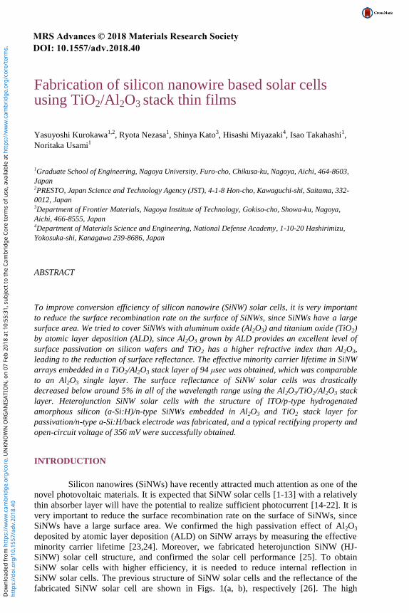
fabricated SiNW solar cell are shown in Figs. 1(a, b), respectively [26]. The high
http
s://
doi.o
rg/1
0.15
57/a
dv.2
018.
40D
ownl
oade
d fr
om h
ttps
://w
ww
.cam
brid
ge.o
rg/c
ore.
UN
KNO
WN
ORG
ANIS
ATIO
N, o
n 07
Feb
201
8 at
10:
55:3
1, s
ubje
ct to
the
Cam
brid
ge C
ore
term
s of
use
, ava
ilabl
e at
htt
ps://
ww
w.c
ambr
idge
.org
/cor
e/te
rms.
reflectance in the infrared region is due to large refractive index mismatch between the p-
type a-Si:H and the n-type SiNWs embedded in Al2O3, since the refractive index of the
SiNW layer was determined by effective medium approximation (EMA) of crystalline
silicon and Al2O3 with a low refractive index of 1.6. In this study, to decrease surface
recombination, we tried to cover SiNWs with aluminum oxide (Al2O3) and titanium
oxide (TiO2) by atomic layer deposition (ALD), since Al2O3 grown by ALD provides an
excellent level of surface passivation on silicon wafers and TiO2 has higher refractive
index than Al2O3, leading to the reduction of surface reflectance. In addition, optical
properties and effective carrier lifetime of the SiNWs with the TiO2/Al2O3 stack layer
were evaluated.
Al2O3
n-type c-Si
p-type a-Si:H
ITO
n-type a-Si:H
Back electrode
50 nm
10 mm
270 mm
50 nm
(a) (b)
400 600 800 1000 12000
0.2
0.4
0.6
0.8
Wavelength (nm)
Reflecta
nce
Figure 1. (a) Schematic diagram of previously reported heterojunction SiNW solar cells [26],
(b) Reflectance spectrum of the SiNW solar cell.
EXPERIMENTAL DETAILS
SiNW arrays were prepared by metal assisted chemical etching with silica
nanoparticles (MACES) [27] on a Si wafer (n-type, (100), 1-5 Ω・cm). Although it is
basically the same as the MACE process [28], silica nanoparticles are used as an etching
mask to control the diameter and density of SiNWs. After the etching of the native oxide
on a Si wafer, the Si wafer was immersed in ethylenediamine (C2H8N2) under a nitrogen
atmosphere for 3 hours at room temperature. The wafer was rinsed with deionized (DI)
water. The hydrophilic Si wafers were immersed in a solution in which 30-nm-silica
nanoparticles modified by carboxyl groups were dispersed at 2 oC for 1 hour. This
process formed a dispersed silica nanoparticle layer on the Si wafer. Subsequently a 20-
nm-thick silver film was deposited on the wafers with silica nanoparticles using a DC
sputtering system. After that, the wafer was chemically etched by using 4.8M HF and
0.15M H2O2 at room temperature to form SiNW arrays. SiNWs with the length of 1, 5,
and 10 μm were prepared on a Si wafer by changing etching duration. The wafers were
put in a HNO3 solution to remove silver particles. Finally, the oxide layer existing on the
surface of the SiNW array was removed with a HF solution. After the fabrication of
SiNW arrays, Al2O3 and TiO2 were deposited by an ALD system (Arradiance, GEM-
STAR6). Trimethylaluminum (Al(CH3)3 (TMA)), tetrakisdimethylaminotitanium
(Ti[N(CH3)2]4), called TDMAT, and H2O were used as aluminum, titanium, and oxygen
reactant sources, respectively. The TDMAT precursor was heated at 60 oC. The
thicknesses of Al2O3 and TiO2 were both 20 nm. The other experimental conditions are
shown in Table I. After the deposition, post-annealing was carried out at 400 oC to
increase negative charge density in the Al2O3 and TiO2.
The structure of SiNW arrays was characterized by field emission scanning
electron microscopy (FE-SEM) and energy dispersive x-ray spectroscopy (EDS) using
JEOL JSM-7001F. The minority carrier lifetime was measured by the μ-PCD method
using KOBELCO LTE-1510EP. The excited wavelength and intensity of incident light
http
s://
doi.o
rg/1
0.15
57/a
dv.2
018.
40D
ownl
oade
d fr
om h
ttps
://w
ww
.cam
brid
ge.o
rg/c
ore.
UN
KNO
WN
ORG
ANIS
ATIO
N, o
n 07
Feb
201
8 at
10:
55:3
1, s
ubje
ct to
the
Cam
brid
ge C
ore
term
s of
use
, ava
ilabl
e at
htt
ps://
ww
w.c
ambr
idge
.org
/cor
e/te
rms.
were 904 nm and 1 ×10¹⁴
cm-2
, respectively. The microwave frequency was 9.6 GHz.
Optical properties of the SiNWs were measured by an UV-VIS-NIR spectrophotometer
(JASCO V-570) and gas-microphone photoacoustic spectroscopy system. The PAS
experimental apparatus consists of a 300 W halogen lamp coupled with a monochrometer
(Jovin-Yvon H20-IR). The photoacoustic (PA) signal was detected by a microphone and
a lock-in amplifier (NF Circuit System 5610B) with a mechanical chopper set at a
frequency of about 20 Hz. The wavelength of the excitation light was scanned from 400
to 1600 nm at 5 nm intervals. PA signal intensity was normalized by the signal from a
fixed quantity of carbon black to eliminate the effects of the wavelength dependence of
the optical apparatus.
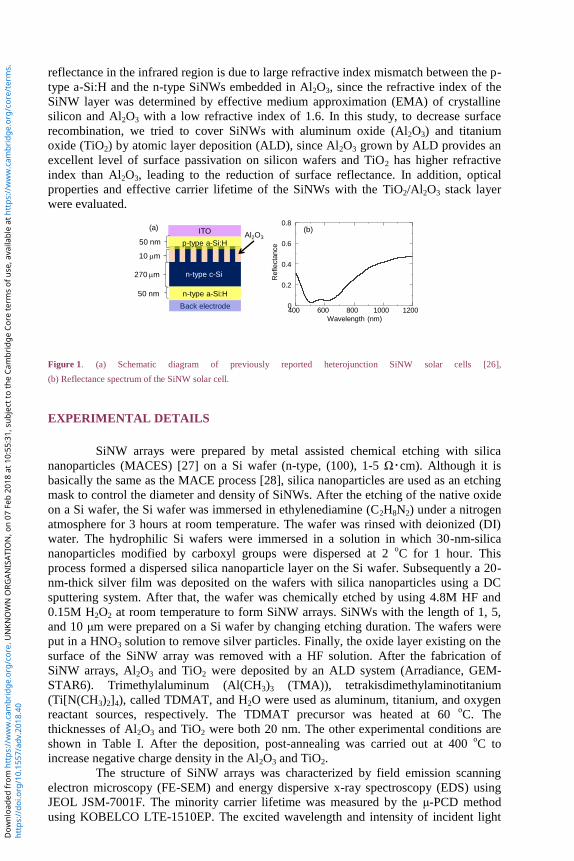
A solar cell structure using SiNW arrays covered with TiO2/Al2O3 stack layers
was fabricated as shown in Fig. 2. SiNW arrays with a length of 10 µm were prepared by
MACES on a Si substrate. After the fabrication of SiNW arrays, 30-nm-thick Al2O3/100-
nm-thick TiO2/470-nm-thick Al2O3 stack layers were deposited on the surface of SiNW
arrays by ALD. After the ALD, SiNW arrays were dipped in 1% HF or were etched by
reactive ion etching (RIE) with a CF4/O2 mixture gas to remove the passivation layer on
only the top of SiNWs. A p-type hydrogenated amorphous silicon (a-Si:H) layer and an
n-type a-Si:H layer were prepared by plasma-enhanced chemical vapor deposition
(PECVD) on the front and back, respectively. Indium tin oxide (ITO) was deposited on
the p-type a-Si:H layer by RF sputtering. Finally, an Al electrode was evaporated on the
back of SiNW solar cells. The final structure was ITO/p-type a-Si:H/n-type SiNW arrays
embedded in TiO2 and Al2O3/n-type a-Si:H/Al. The surface reflectance of the SiNW
solar cells was evaluated by UV-VIS-NIR spectrophotometers with SHIMADZU Solid
Spec-3700. The solar cells were characterized by dark and illuminated J-V characteristics
under AM1.5G illumination.
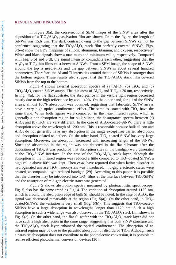
Table I. Deposition conditions of Al2O3 and TiO2.
Materials Al2O3 TiO2
Temperature 200 oC 225
oC
Cycles 350 144
Flow duration
TMA: 200 msec TDMAT: 700 msec
H2O: 200 msec H2O: 22 msec
n-type a-Si:H
Al
n-type c-Si
50 nm
10 µm
270 µm
p-type a-Si:H50 nm
ITO
n-type SiNW array
with TiO2/Al2O3
p-type a-Si:H
Al2O3 TiO230 nm 100 nm
Figure 2. Schematic diagram of the fabricated solar cell structure including SiNW arrays covered with Al2O3/TiO2/Al2O3
stack layers.
http
s://
doi.o
rg/1
0.15
57/a
dv.2
018.
40D
ownl
oade
d fr
om h
ttps
://w
ww
.cam
brid
ge.o
rg/c
ore.
UN
KNO
WN
ORG
ANIS
ATIO
N, o
n 07
Feb
201
8 at
10:
55:3
1, s
ubje
ct to
the
Cam
brid
ge C
ore
term
s of
use
, ava
ilabl
e at
htt
ps://
ww
w.c
ambr
idge
.org
/cor
e/te
rms.
RESULTS AND DISCUSSION
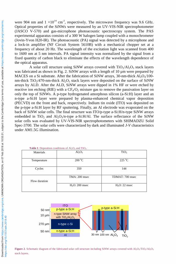
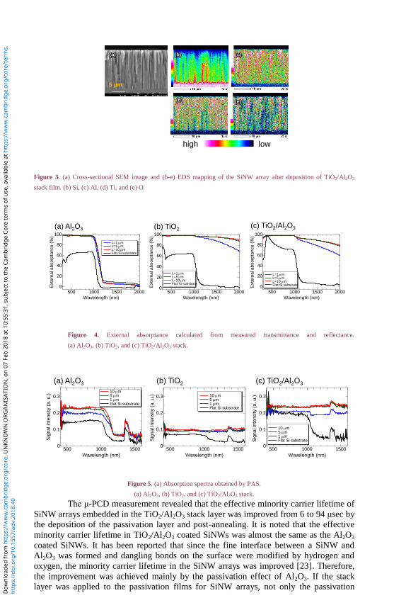
In Figure 3(a), the cross-sectional SEM images of the SiNW array after the
deposition of a TiO2/Al2O3 passivation film are shown. From the figure, the length of
SiNWs was 15.6 µm. The dark contrast owing to the gap between SiNWs cannot be
confirmed, suggesting that the TiO2/Al2O3 stack film perfectly covered SiNWs. Figs.
3(b-e) show the EDS mappings of silicon, aluminum, titanium, and oxygen, respectively.
White and black signals show a maximum and minimum value, respectively. Compared
with Fig. 3(b) and 3(d), the signal intensity contradicts each other, suggesting that the
Al2O3 or TiO2 thin films exist between SiNWs. From a SEM image, the shape of SiNWs
around the top is needle-like and the gap between SiNWs is about several hundred
nanometers. Therefore, the Al and Ti intensities around the top of SiNWs is stronger than
the bottom region. These results also suggest that the TiO2/Al2O3 stack film covered
SiNWs from the top to the bottom.
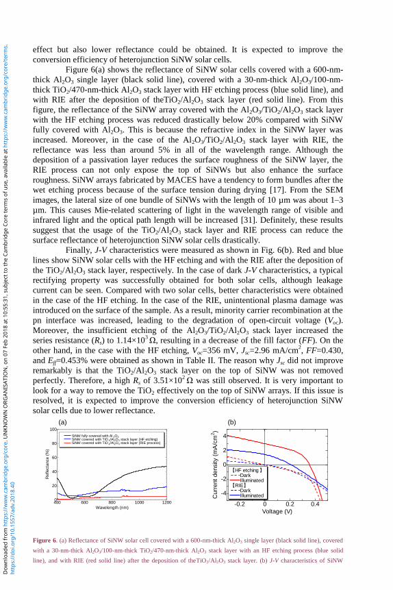
Figure 4 shows external absorption spectra of (a) Al2O3, (b) TiO2, and (c)
TiO2/Al2O3 coated SiNW arrays. The thickness of Al2O3 and TiO2 is 20 nm, respectively.
In Fig. 4(a), for the flat substrate, the absorptance in the visible light region decreased
mostly due to the high reflectance by about 40%. On the other hand, for all of the SiNW
arrays, almost 100% absorption was obtained, suggesting that fabricated SiNW arrays
have a very high optical confinement effect. The samples coated with TiO2 have the
same trend. When both figures were compared, in the near-infrared region, which is
generally a non-absorption region for bulk silicon, the absorptance spectra between (a)
Al2O3 and (b) TiO2 are very different. In the case of Al2O3-coated-SiNW, there is little
absorption above the wavelength of 1200 nm. This is reasonable because bulk silicon and
Al2O3 do not generally have any absorption in the range except free carrier absorption
and absorption related to defects. On the other hand, TiO2-coated-SiNW has very large
absorption. Moreover, the absorption increased with increasing length of the SiNWs.
Since the absorption in the region was not detected in the flat substrate after the
deposition of TiO2, it was predicted that absorption sites in the bandgap were generated
at the TiO2/SiNW interface. In the case of the TiO2/Al2O3 stack layer, although the
absorption in the infrared region was reduced a little compared to TiO2-coated SiNW, a
high value above 80% was kept. Chen et al. have reported that when lattice disorder in
hydrogenated anatase TiO2 nanocrystals was introduced, mid-gap electronic states were
created, accompanied by a reduced bandgap [29]. According to this paper, it is possible
that the disorder may be introduced into TiO2 films at the interface between TiO2/SiNW
and the absorption of mid-gap electric states was generated.
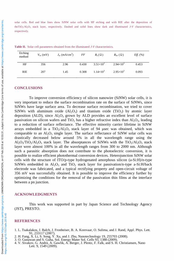
Figure 5 shows absorption spectra measured by photoacoustic spectroscopy.
Fig. 5 also has the same trend as Fig. 4. The variation of absorption around 1120 nm,
which is around the absorption edge of bulk Si, should be noted. In the case of Al2O3, the
signal was decreased remarkably at the region (Fig. 5(a)). On the other hand, in TiO2-
coated-SiNWs, the variation is very small (Fig. 5(b)). This suggests that TiO2-coated-
SiNWs have a large absorption in wavelengths longer than 1120 nm. Such a high
absorption in such a wide range was also observed in the TiO2/Al2O3 stack film shown in
Fig. 5(c). On the other hand, the flat Si wafer with the TiO2/Al2O3 stack layer did not
have such a high absorption in the same range, suggesting that both SiNW structure and
the TiO2/Al2O3 stack layer enhanced the optical confinement. The absorption of an
infrared region may be due to the parasitic absorption of disordered TiO2. Although such
a parasitic absorption does not contribute to the photoelectric conversion, it is possible to
realize efficient photothermal conversion devices [30].
http
s://
doi.o
rg/1
0.15
57/a
dv.2
018.
40D
ownl
oade
d fr
om h
ttps
://w
ww
.cam
brid
ge.o
rg/c
ore.
UN
KNO
WN
ORG
ANIS
ATIO
N, o
n 07
Feb
201
8 at
10:
55:3
1, s
ubje
ct to
the
Cam
brid
ge C
ore
term
s of
use
, ava
ilabl
e at
htt
ps://
ww
w.c
ambr
idge
.org
/cor
e/te
rms.
5 µm
high low
(a) (b) (c)
(d) (e)
Figure 3. (a) Cross-sectional SEM image and (b-e) EDS mapping of the SiNW array after deposition of TiO2/Al2O3
stack film. (b) Si, (c) Al, (d) Ti, and (e) O.
(a) Al2O3 (b) TiO2
500 1000 1500 2000
0
20
40
60
80
100
Wavelength (nm)
Exte
rnal absorp
tance (
%)
L=1 mm L=5 mm L=10 mm Flat Si substrate
500 1000 1500 20000
20
40
60
80
100
Wavelength (nm)
Exte
rnal absorp
tance (
%)
L=1 mm L=5 mm L=10 mm Flat Si substrate
(c) TiO2/Al2O3
500 1000 1500 2000
0
20
40
60
80
100
Wavelength (nm)
Exte
rnal absorp
tance (
%)
L=1 mm L=5 mm L=10 mm Flat Si substrate
Figure 4. External absorptance calculated from measured transmittance and reflectance.
(a) Al2O3, (b) TiO2, and (c) TiO2/Al2O3 stack.
(a) Al2O3 (b) TiO2
500 1000 15000
0.1
0.2
0.3
Wavelength (nm)
Sig
nal in
tensity (
a.
u.)
10 mm 5 mm 1 mm Flat Si substrate
500 1000 15000
0.1
0.2
0.3
Wavelength (nm)
Sig
nal in
tensity (
a.
u.) 10 mm
5 mm 1 mm Flat Si substrate
500 1000 15000
0.1
0.2
0.3
Wavelength (nm)
Sig
nal in
tensity (
a.
u.)
10 mm 5 mm 1 mm Flat Si substrate
(c) TiO2/Al2O3
Figure 5. (a) Absorption spectra obtained by PAS.
(a) Al2O3, (b) TiO2, and (c) TiO2/Al2O3 stack.
The μ-PCD measurement revealed that the effective minority carrier lifetime of
SiNW arrays embedded in the TiO2/Al2O3 stack layer was improved from 6 to 94 μsec by
the deposition of the passivation layer and post-annealing. It is noted that the effective
minority carrier lifetime in TiO2/Al2O3 coated SiNWs was almost the same as the Al2O3
coated SiNWs. It has been reported that since the fine interface between a SiNW and
Al2O3 was formed and dangling bonds on the surface were modified by hydrogen and
oxygen, the minority carrier lifetime in the SiNW arrays was improved [23]. Therefore,
the improvement was achieved mainly by the passivation effect of Al2O3. If the stack
layer was applied to the passivation films for SiNW arrays, not only the passivation
http
s://
doi.o
rg/1
0.15
57/a
dv.2
018.
40D
ownl
oade
d fr
om h
ttps
://w
ww
.cam
brid
ge.o
rg/c
ore.
UN
KNO
WN
ORG
ANIS
ATIO
N, o
n 07
Feb
201
8 at
10:
55:3
1, s
ubje
ct to
the
Cam
brid
ge C
ore
term
s of
use
, ava
ilabl
e at
htt
ps://
ww
w.c
ambr
idge
.org
/cor
e/te
rms.
effect but also lower reflectance could be obtained. It is expected to improve the
conversion efficiency of heterojunction SiNW solar cells.
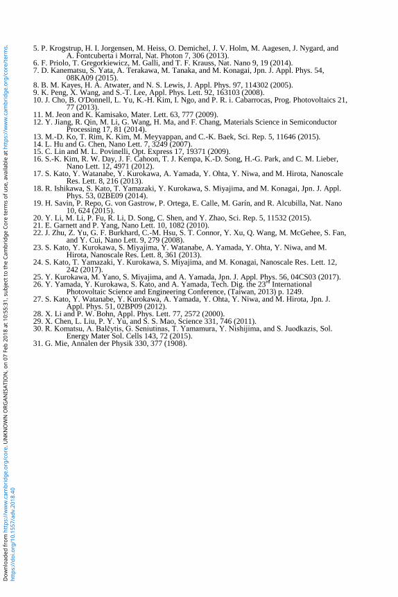
Figure 6(a) shows the reflectance of SiNW solar cells covered with a 600-nm-
thick Al2O3 single layer (black solid line), covered with a 30-nm-thick Al2O3/100-nm-
thick TiO2/470-nm-thick Al2O3 stack layer with HF etching process (blue solid line), and
with RIE after the deposition of theTiO2/Al2O3 stack layer (red solid line). From this
figure, the reflectance of the SiNW array covered with the Al2O3/TiO2/Al2O3 stack layer
with the HF etching process was reduced drastically below 20% compared with SiNW
fully covered with Al2O3. This is because the refractive index in the SiNW layer was
increased. Moreover, in the case of the Al2O3/TiO2/Al2O3 stack layer with RIE, the
reflectance was less than around 5% in all of the wavelength range. Although the
deposition of a passivation layer reduces the surface roughness of the SiNW layer, the
RIE process can not only expose the top of SiNWs but also enhance the surface
roughness. SiNW arrays fabricated by MACES have a tendency to form bundles after the
wet etching process because of the surface tension during drying [17]. From the SEM
images, the lateral size of one bundle of SiNWs with the length of 10 µm was about 1–3
µm. This causes Mie-related scattering of light in the wavelength range of visible and
infrared light and the optical path length will be increased [31]. Definitely, these results
suggest that the usage of the TiO2/Al2O3 stack layer and RIE process can reduce the
surface reflectance of heterojunction SiNW solar cells drastically.
Finally, J-V characteristics were measured as shown in Fig. 6(b). Red and blue
lines show SiNW solar cells with the HF etching and with the RIE after the deposition of
the TiO2/Al2O3 stack layer, respectively. In the case of dark J-V characteristics, a typical
rectifying property was successfully obtained for both solar cells, although leakage
current can be seen. Compared with two solar cells, better characteristics were obtained
in the case of the HF etching. In the case of the RIE, unintentional plasma damage was
introduced on the surface of the sample. As a result, minority carrier recombination at the
pn interface was increased, leading to the degradation of open-circuit voltage (Voc).
Moreover, the insufficient etching of the Al2O3/TiO2/Al2O3 stack layer increased the
series resistance (Rs) to 1.14×10³ Ω, resulting in a decrease of the fill factor (FF). On the
other hand, in the case with the HF etching, Voc=356 mV, Jsc=2.96 mA/cm2, FF=0.430,
and Eff=0.453% were obtained as shown in Table II. The reason why Jsc did not improve
remarkably is that the TiO2/Al2O3 stack layer on the top of SiNW was not removed
perfectly. Therefore, a high Rs of 3.51×10²
Ω was still observed. It is very important to
look for a way to remove the TiO2 effectively on the top of SiNW arrays. If this issue is
resolved, it is expected to improve the conversion efficiency of heterojunction SiNW
solar cells due to lower reflectance.
-0.2 0 0.2 0.4
-4
-2
0
2
4
Voltage (V)
Curr
ent
density (
mA
/cm
2)
【HF etching】DarkIlluminated
【RIE】DarkIlluminated
(a) (b)
400 600 800 1000 12000
20
40
60
80
100
Wavelength (nm)
Reflecta
nce (
%)
SiNW fully covered with Al 2O3 SiNW covered with TiO 2/Al2O3 stack layer (HF etching) SiNW covered with TiO 2/Al2O3 stack layer (RIE process)
Figure 6. (a) Reflectance of SiNW solar cell covered with a 600-nm-thick Al2O3 single layer (black solid line), covered
with a 30-nm-thick Al2O3/100-nm-thick TiO2/470-nm-thick Al2O3 stack layer with an HF etching process (blue solid
line), and with RIE (red solid line) after the deposition of theTiO2/Al2O3 stack layer. (b) J-V characteristics of SiNW
http
s://
doi.o
rg/1
0.15
57/a
dv.2
018.
40D
ownl
oade
d fr
om h
ttps
://w
ww
.cam
brid
ge.o
rg/c
ore.
UN
KNO
WN
ORG
ANIS
ATIO
N, o
n 07
Feb
201
8 at
10:
55:3
1, s
ubje
ct to
the
Cam
brid
ge C
ore
term
s of
use
, ava
ilabl
e at
htt
ps://
ww
w.c
ambr
idge
.org
/cor
e/te
rms.
solar cells. Red and blue lines show SiNW solar cells with HF etching and with RIE after the deposition of
theTiO2/Al2O3 stack layer, respectively. Dashed and solid lines show dark and illuminated J-V characteristics,
respectively.
Table II. Solar cell parameters obtained from the illuminated J-V characteristics.
Etching
method Voc (mV) Jsc (mA/cm
2) FF Rs (Ω) Rsh (Ω) Eff. (%)
HF 356 2.96 0.430 3.51×10² 2.94×10
3 0.453
RIE 207 1.45 0.308 1.14×10³ 2.95×10
3 0.093
CONCLUSIONS
To improve conversion efficiency of silicon nanowire (SiNW) solar cells, it is
very important to reduce the surface recombination rate on the surface of SiNWs, since
SiNWs have large surface area. To decrease surface recombination, we tried to cover
SiNWs with aluminum oxide (Al2O3) and titanium oxide (TiO2) by atomic layer
deposition (ALD), since Al2O3 grown by ALD provides an excellent level of surface
passivation on silicon wafers and TiO2 has a higher refractive index than Al2O3, leading
to a reduction of surface reflectance. The effective minority carrier lifetime in SiNW
arrays embedded in a TiO2/Al2O3 stack layer of 94 μsec was obtained, which was
comparable to an Al2O3 single layer. The surface reflectance of SiNW solar cells was
drastically decreased below around 5% in all the wavelength range using the
Al2O3/TiO2/Al2O3 stack layer. The absorptances of SiNWs with the TiO2/Al2O3 stack
layer were almost 100% in all the wavelength ranges from 300 to 2000 nm. Although
such a parasitic absorption does not contribute to the photoelectric conversion, it is
possible to realize efficient photothermal conversion devices. Heterojunction SiNW solar
cells with the structure of ITO/p-type hydrogenated amorphous silicon (a-Si:H)/n-type
SiNWs embedded in Al2O3 and TiO2 stack layer for passivation/n-type a-Si:H/back
electrode was fabricated, and a typical rectifying property and open-circuit voltage of
356 mV was successfully obtained. It is possible to improve the efficiency further by
optimizing the conditions for the removal of the passivation thin films at the interface
between a pn junction.
ACKNOWLEDGMENTS
This work was supported in part by Japan Science and Technology Agency
(JST), PRESTO.
REFERENCES
1. L. Tsakalakos, J. Balch, J. Fronheiser, B. A. Korevaar, O. Sulima, and J. Rand, Appl. Phys. Lett. 91, 233117 (2007).
2. H. Fang, X. Li, S. Song, Y. Xu, and J. Zhu, Nanotechnology 19, 255703 (2008). 3. O. Gunawan and S. Guha, Sol. Energy Mater Sol. Cells 93, 1388 (2009). 4. V. Sivakov, G. Andrä, A. Gawlik, A. Berger, J. Plentz, F. Falk, and S. H. Christiansen, Nano
Lett. 9, 1549 (2009).
http
s://
doi.o
rg/1
0.15
57/a
dv.2
018.
40D
ownl
oade
d fr
om h
ttps
://w
ww
.cam
brid
ge.o
rg/c
ore.
UN
KNO
WN
ORG
ANIS
ATIO
N, o
n 07
Feb
201
8 at
10:
55:3
1, s
ubje
ct to
the
Cam
brid
ge C
ore
term
s of
use
, ava
ilabl
e at
htt
ps://
ww
w.c
ambr
idge
.org
/cor
e/te
rms.
5. P. Krogstrup, H. I. Jorgensen, M. Heiss, O. Demichel, J. V. Holm, M. Aagesen, J. Nygard, and A. Fontcuberta i Morral, Nat. Photon 7, 306 (2013).
6. F. Priolo, T. Gregorkiewicz, M. Galli, and T. F. Krauss, Nat. Nano 9, 19 (2014). 7. D. Kanematsu, S. Yata, A. Terakawa, M. Tanaka, and M. Konagai, Jpn. J. Appl. Phys. 54,
08KA09 (2015). 8. B. M. Kayes, H. A. Atwater, and N. S. Lewis, J. Appl. Phys. 97, 114302 (2005). 9. K. Peng, X. Wang, and S.-T. Lee, Appl. Phys. Lett. 92, 163103 (2008). 10. J. Cho, B. O'Donnell, L. Yu, K.-H. Kim, I. Ngo, and P. R. i. Cabarrocas, Prog. Photovoltaics 21,
77 (2013). 11. M. Jeon and K. Kamisako, Mater. Lett. 63, 777 (2009). 12. Y. Jiang, R. Qin, M. Li, G. Wang, H. Ma, and F. Chang, Materials Science in Semiconductor
Processing 17, 81 (2014). 13. M.-D. Ko, T. Rim, K. Kim, M. Meyyappan, and C.-K. Baek, Sci. Rep. 5, 11646 (2015). 14. L. Hu and G. Chen, Nano Lett. 7, 3249 (2007). 15. C. Lin and M. L. Povinelli, Opt. Express 17, 19371 (2009). 16. S.-K. Kim, R. W. Day, J. F. Cahoon, T. J. Kempa, K.-D. Song, H.-G. Park, and C. M. Lieber,
Nano Lett. 12, 4971 (2012). 17. S. Kato, Y. Watanabe, Y. Kurokawa, A. Yamada, Y. Ohta, Y. Niwa, and M. Hirota, Nanoscale
Res. Lett. 8, 216 (2013). 18. R. Ishikawa, S. Kato, T. Yamazaki, Y. Kurokawa, S. Miyajima, and M. Konagai, Jpn. J. Appl.
Phys. 53, 02BE09 (2014). 19. H. Savin, P. Repo, G. von Gastrow, P. Ortega, E. Calle, M. Garín, and R. Alcubilla, Nat. Nano
10, 624 (2015). 20. Y. Li, M. Li, P. Fu, R. Li, D. Song, C. Shen, and Y. Zhao, Sci. Rep. 5, 11532 (2015). 21. E. Garnett and P. Yang, Nano Lett. 10, 1082 (2010). 22. J. Zhu, Z. Yu, G. F. Burkhard, C.-M. Hsu, S. T. Connor, Y. Xu, Q. Wang, M. McGehee, S. Fan,
and Y. Cui, Nano Lett. 9, 279 (2008). 23. S. Kato, Y. Kurokawa, S. Miyajima, Y. Watanabe, A. Yamada, Y. Ohta, Y. Niwa, and M.
Hirota, Nanoscale Res. Lett. 8, 361 (2013). 24. S. Kato, T. Yamazaki, Y. Kurokawa, S. Miyajima, and M. Konagai, Nanoscale Res. Lett. 12,
242 (2017). 25. Y. Kurokawa, M. Yano, S. Miyajima, and A. Yamada, Jpn. J. Appl. Phys. 56, 04CS03 (2017). 26. Y. Yamada, Y. Kurokawa, S. Kato, and A. Yamada, Tech. Dig. the 23
rd International
Photovoltaic Science and Engineering Conference, (Taiwan, 2013) p. 1249. 27. S. Kato, Y. Watanabe, Y. Kurokawa, A. Yamada, Y. Ohta, Y. Niwa, and M. Hirota, Jpn. J.
Appl. Phys. 51, 02BP09 (2012). 28. X. Li and P. W. Bohn, Appl. Phys. Lett. 77, 2572 (2000). 29. X. Chen, L. Liu, P. Y. Yu, and S. S. Mao, Science 331, 746 (2011). 30. R. Komatsu, A. Balčytis, G. Seniutinas, T. Yamamura, Y. Nishijima, and S. Juodkazis, Sol.
Energy Mater Sol. Cells 143, 72 (2015). 31. G. Mie, Annalen der Physik 330, 377 (1908).
http
s://
doi.o
rg/1
0.15
57/a
dv.2
018.
40D
ownl
oade
d fr
om h
ttps
://w
ww
.cam
brid
ge.o
rg/c
ore.
UN
KNO
WN
ORG
ANIS
ATIO
N, o
n 07
Feb
201
8 at
10:
55:3
1, s
ubje
ct to
the
Cam
brid
ge C
ore
term
s of
use
, ava
ilabl
e at
htt
ps://
ww
w.c
ambr
idge
.org
/cor
e/te
rms.