Embed Size (px)
Citation preview
H. Wang1, J. X. Wang1, A. B. Prakoso1,2, and Rusli 1,2
1School of Electrical and Electronic Engineering,
Nanyang Technological University, Singapore 2CINTRA UMI CNRS/NTU/THALES 3288, Research Techno
Plaza, NTU, Singapore
email: [email protected]
Thin Film Silicon Nanowire/PEDOT:PSS
Hybrid Solar Cells with Surface Treatment
1

Nanyang Technological University
Singapore 2
Outline
Introduction
SiNWs/PEDOT:PSS hybrid cell
Experiments, results and discussions
Fabrication of thin film SiNWs/PEDOT:PSS cells
Two-step surface treatment
Characterization of hybrid cells
Conclusions
3
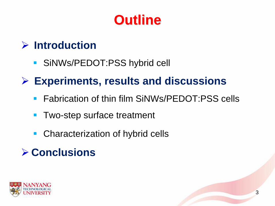
Inorganic solar cells High carriers mobility
High PCE & stability
High material cost
Complex fabrication
Organic solar cells Low material cost
Simple solution process
Low carriers mobility
Low PCE & poor lifetime
Hybrid solar cells Combined advantages
Introduction
4
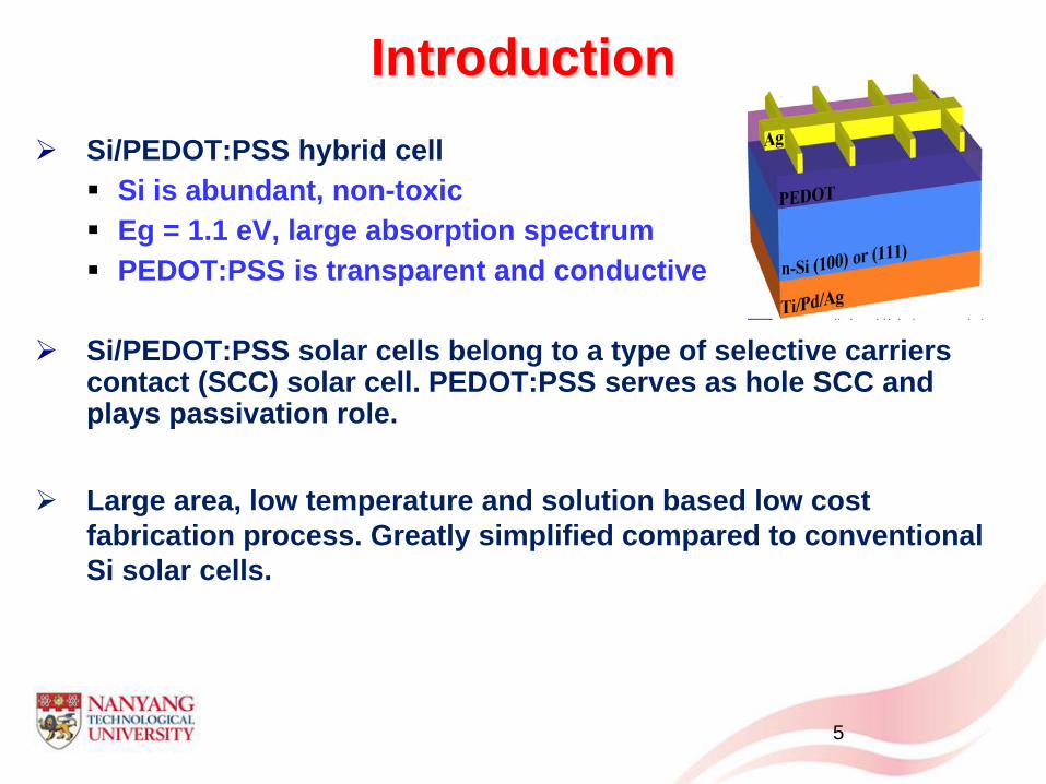
Si/PEDOT:PSS hybrid cell
Si is abundant, non-toxic
Eg = 1.1 eV, large absorption spectrum
PEDOT:PSS is transparent and conductive
Si/PEDOT:PSS solar cells belong to a type of selective carriers contact (SCC) solar cell. PEDOT:PSS serves as hole SCC and plays passivation role.
Large area, low temperature and solution based low cost
fabrication process. Greatly simplified compared to conventional
Si solar cells.
Introduction
5
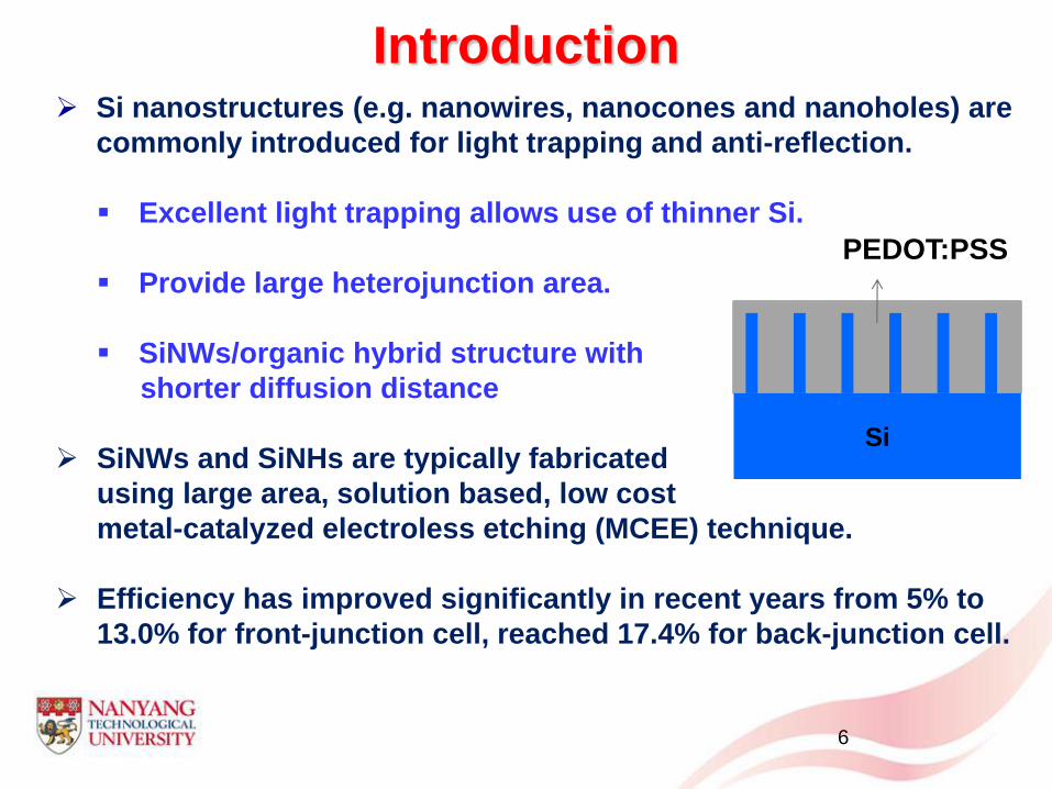
Si nanostructures (e.g. nanowires, nanocones and nanoholes) are
commonly introduced for light trapping and anti-reflection.
Excellent light trapping allows use of thinner Si.
Provide large heterojunction area.
SiNWs/organic hybrid structure with
shorter diffusion distance
SiNWs and SiNHs are typically fabricated
using large area, solution based, low cost
metal-catalyzed electroless etching (MCEE) technique.
Efficiency has improved significantly in recent years from 5% to
13.0% for front-junction cell, reached 17.4% for back-junction cell.
Introduction
Si
PEDOT:PSS
6
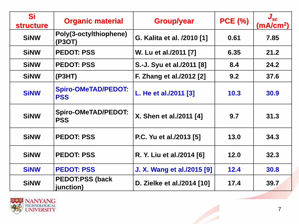
Si
structure Organic material Group/year PCE (%)
Jsc
(mA/cm2)
SiNW Poly(3-octylthiophene)
(P3OT) G. Kalita et al. /2010 [1] 0.61 7.85
SiNW PEDOT: PSS W. Lu et al./2011 [7] 6.35 21.2
SiNW PEDOT: PSS S.-J. Syu et al./2011 [8] 8.4 24.2
SiNW (P3HT) F. Zhang et al./2012 [2] 9.2 37.6
SiNW Spiro-OMeTAD/PEDOT:
PSS L. He et al./2011 [3] 10.3 30.9
SiNW Spiro-OMeTAD/PEDOT:
PSS X. Shen et al./2011 [4] 9.7 31.3
SiNW PEDOT: PSS P.C. Yu et al./2013 [5] 13.0 34.3
SiNW PEDOT: PSS R. Y. Liu et al./2014 [6] 12.0 32.3
SiNW PEDOT: PSS J. X. Wang et al./2015 [9] 12.4 30.8
SiNW PEDOT:PSS (back
junction) D. Zielke et al./2014 [10] 17.4 39.7
7
References 1 G. Kalita, S. Adhikari, H. R. Aryal, R. Afre, T. Soga, M. Sharon, W. Koichi, and M.
Umeno, Journal of Physics D: Applied Physics 42, 115104 (5 pp.) (2009).
2 F. Zhang, X. Han, S.-T. Lee, and B. Sun, Journal of Materials Chemistry 22, 5362-5368
(2012).
3 L. He, C. Jiang, Rusli, D. Lai, and H. Wang, Applied Physics Letters 99, 021104-6
(2011).
4 X. Shen, B. Sun, D. Liu, and S.-T. Lee, Journal of the American Chemical Society 133,
19408-19415 (2011).
5 P. C. Yu, C. Y. Tsai, J. K. Chang, C. C. Lai, P. H. Chen, Y. C. Lai, P. T. Tsai, M. C. Li, H.
T. Pan, Y. Y. Huang, C. I. Wu, Y. L. Chueh, S. W. Chen, C. H. Du, S. F. Horng, H. F.
Meng, Acs Nano 7, 10780-10787 (2013).
6 R. Y. Liu, S. T. Lee, and B. Q. Sun, Advanced materials 26, 6007-6012 (2014).
7 W. Lu, C. Wang, W. Yue, and L. Chen, Nanoscale 3, 3631-3634 (2011).
8 H.-J. Syu, S.-C. Shiu, and C.-F. Lin, Solar Energy Materials and Solar Cells 98, 267-272
(2012).
9 Jianxiong Wang et. al, Nanoscale, Vol 7, 4559-65 (2015)
10 D. Zielke, A. Pazidis, F.Werner and J. Schmidt, Solar Energy Materials &Solar Cell 131,
110-116 (2014).
8

Hybrid Si/PEDOT:PSS Solar Cells Year Strucutre PCE (%)
2011 SiNW/SPIRO hybrid cell1 10.3
2011 SiNW/PEDOT hybrid cell2 9.0
2012 Pymarids/SiNWs/PEDOT hybrid solar cells3 9.9
2012 Planar Si/PEDOT hybrid cell4 10.6
2012 SiNWs/ PEDOT hybrid cell with 2.2um epitaxial Si5 5.6
2014 SiNH/PEDOT hybrid cell6 8.3
2015 SiNW/PEDOT hybrid cell with surface treatment7 12.4
2016 Planar Si/PEDOT hybrid cell with 15.5um epitaxial Si8 8.7
2016 SiNH/PEDOT hybrid cell9 12.9 1 L. He et. al, Applied Physics Letters 99, 021104-6 (2011). 2 L. He et. al, IEEE Electron Device Letters, 32, pp. 1406-8 (2011). 3 L. He et. al, Small, vol 8, pp. 1664-1668, (2012). 4 L. He et. al, Applied Physics Letters, vol. 100, pp. 073503-5 (2012). 5 L. He et. al, Applied Physics Letters, vol 100, pp. 103104-7 (2012) 6 L. Hong et. al, Applied Physics Letters, vol 104, 053104 (2014) 7 J. X. Wang et. al, Nanoscale, Vol 7, 4559-65 (2015) 8 H. Wang et al, IEEE Journal of Photovoltaics 6, 217 (2016). 9 Z. Y. Li et. al, EU PVSEC (2016)
9
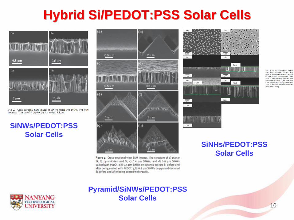
Hybrid Si/PEDOT:PSS Solar Cells
SiNWs/PEDOT:PSS
Solar Cells
Pyramid/SiNWs/PEDOT:PSS
Solar Cells
SiNHs/PEDOT:PSS
Solar Cells
10

The efficiencies of hybrid solar cell based on Si
nanostructures are not much better than planar cell,
despite their excellent light trapping properties.
Jsc is increased but Voc is substantially lowered.
Attributed to the severe carriers recombination
associated with the defective surface.
Introduction
11
Defective SiNWs surface
Dry etching ion bombard damage of the surface
Metal catalyze electroless etching (MCEE)
Large surface area of the nanostructures
PEDOT:PSS layer is not fully penetrated into the gaps
of SiNWs
Long molecular chain of PEDOT:PSS and its fast
drying process
Agglomeration of the long nanowires
Introduction
12
Various approaches can reduce the recombination of
nanostructures
Surface passivation
Attaching some chemical molecules to the Si surface.
E.g. CH3-temination
Using native oxides as passivation layer. SiOx have
been commonly used for passivation.
Optimized nanostructures
Shrinking surface area but not sacrificing their light
absorption. (e.g. inverted nanopyramid, nanoholes)
Introduction
13

Nanowires/PEDOT:PSS
hybrid cells on thin film Si with
surface treatment
14
We applied a two-step surface treatment to hybrid
SiNWs/PEDOT:PSS solar cells.
Treated with O2 plasma surface treatment to grow oxide,
which embeds the Ag nanoparticles. Oxide is then
partially removed and leave behind a thin layer for
passivation.
Si/PEDOT:PSS hybrid cells are demonstrated on thin
film Si to lower the material cost.
SiNWs with different lengths are investigated.
Introduction
15
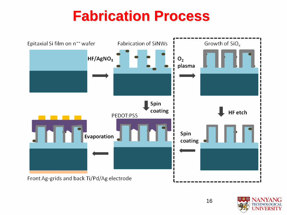
Fabrication Process
16
Fabrication Details 10.6 µm epitaxial single crystal (100) Si film grown by HTCVD on
n++ Si (100) substrates using dichlorosilane precursor and
phosphine (PH3) dopant gas at 1000 oC.
MCEE: etching solution of 4.6 M HF and 0.02 M AgNO3 at room
temperature to fabricate the SiNWs
SiNWs
Length: 0.4 to 2.7 µm
Diameter: 20 to 100 nm
Gap between SiNWs: < 50 nm
O2 plasma treatment 480 sec : 30 sccm, RF power of 30 watts and
pressure of 200 mTorr.
SiNWs were etched in a 5% HF solution for 85 s to reduce the
thickness of the surface oxide and obtain a cleaner surface
PEDOT:PSS thickness: 80 mn
Back contact Ti/Pd/Ag: 50nm : 50nm : 1000 nm
Front contact Ag: 1000 nm
Active area of cell: 0.95 cm2. 17
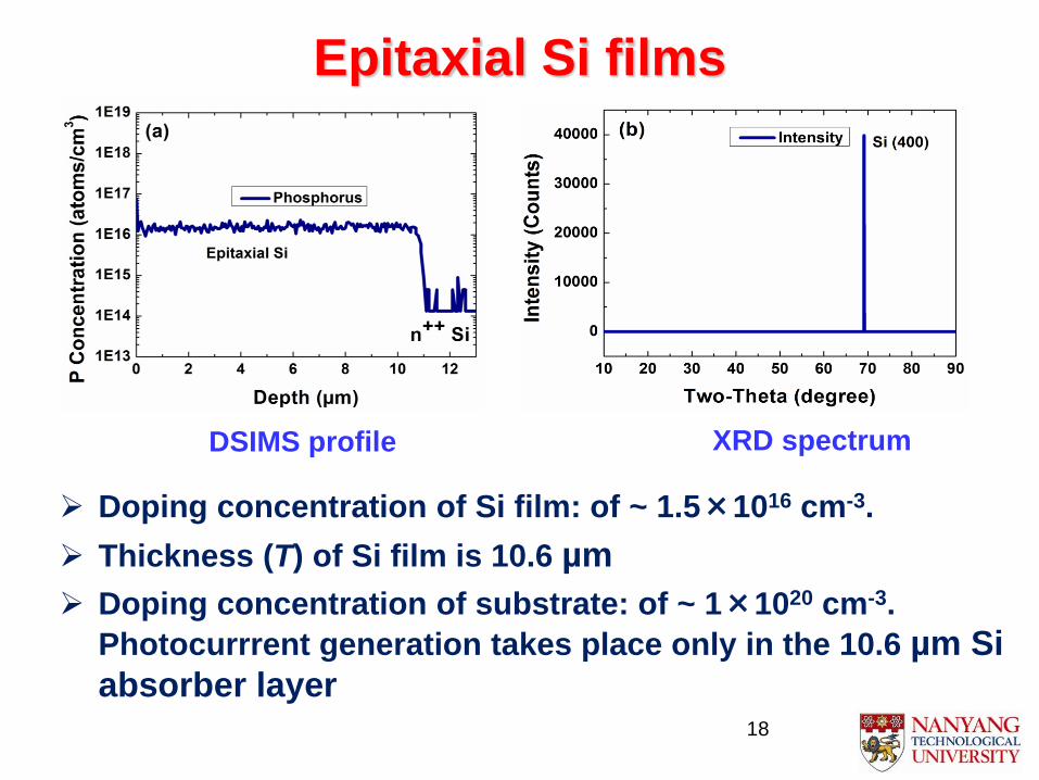
Epitaxial Si films
DSIMS profile XRD spectrum
Doping concentration of Si film: of ~ 1.5×1016 cm-3.
Thickness (T) of Si film is 10.6 µm
Doping concentration of substrate: of ~ 1×1020 cm-3.
Photocurrrent generation takes place only in the 10.6 µm Si
absorber layer 18
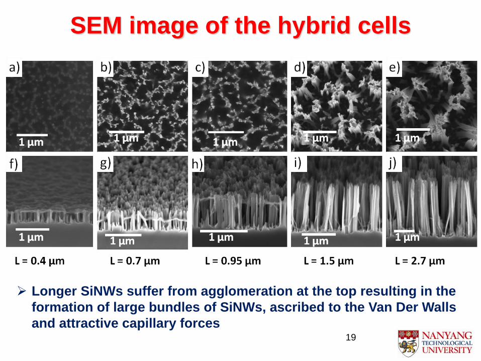
SEM image of the hybrid cells
top view
cross-section cross-section
Longer SiNWs suffer from agglomeration at the top resulting in the
formation of large bundles of SiNWs, ascribed to the Van Der Walls
and attractive capillary forces 19

SEM image of the hybrid cells
top view
Treated SiNWs reveal a smoother surface coverage of
PEDOT:PSS layer 20
untreated treated untreated treated
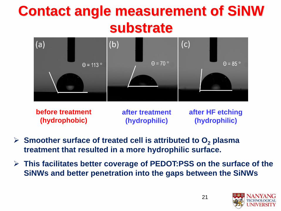
before treatment
(hydrophobic)
Contact angle measurement of SiNW
substrate
Smoother surface of treated cell is attributed to O2 plasma
treatment that resulted in a more hydrophilic surface.
This facilitates better coverage of PEDOT:PSS on the surface of the
SiNWs and better penetration into the gaps between the SiNWs
after HF etching
(hydrophilic)
after treatment
(hydrophilic)
21
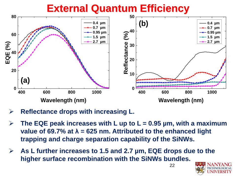
Reflectance drops with increasing L.
The EQE peak increases with L up to L = 0.95 µm, with a maximum
value of 69.7% at λ = 625 nm. Attributed to the enhanced light
trapping and charge separation capability of the SiNWs.
As L further increases to 1.5 and 2.7 µm, EQE drops due to the
higher surface recombination with the SiNWs bundles.
External Quantum Efficiency
400 600 800 10000
20
40
60
80
EQ
E (
%)
Wavelength (nm)
0.4 µm
0.7 µm
0.95 µm
1.5 µm
2.7 µm
(a)
400 600 800 10000
10
20
30
40
50
Refl
ecta
nce (
%)
Wavelength (nm)
0.4 µm
0.7 µm
0.95 µm
1.5 µm
2.7 µm
(b)
22
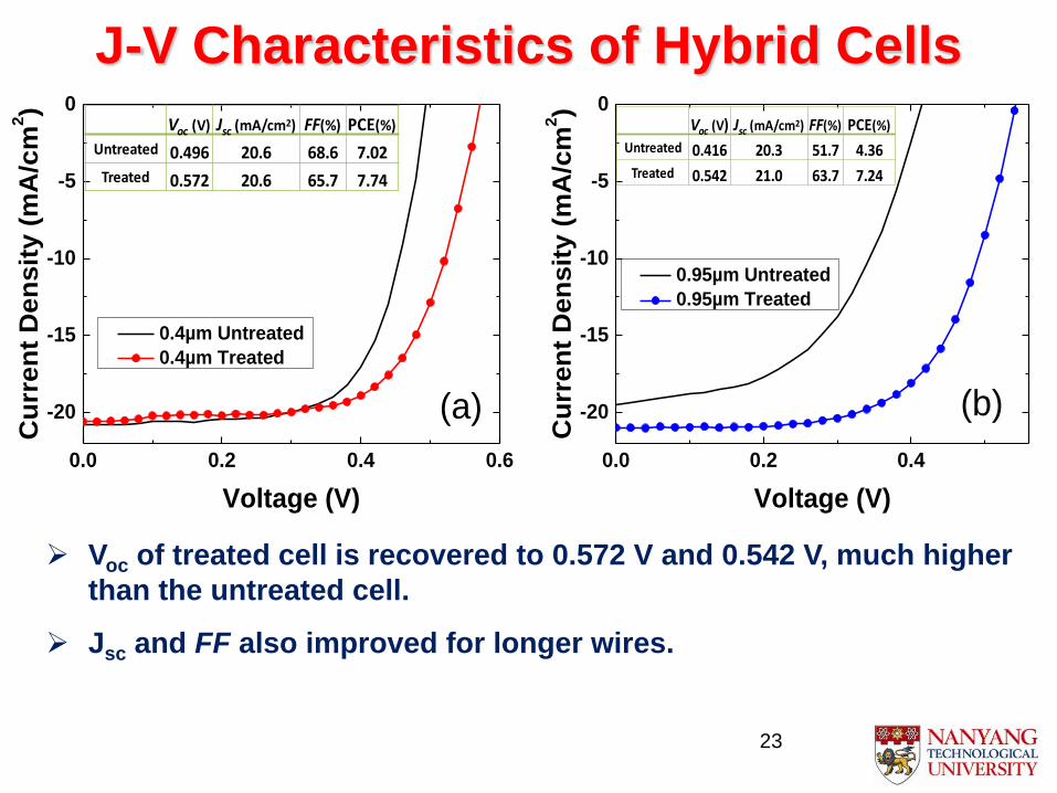
J-V Characteristics of Hybrid Cells
0.0 0.2 0.4 0.6
-20
-15
-10
-5
0Voc (V) Jsc (mA/cm2) FF(%) PCE(%)
Untreated 0.496 20.6 68.6 7.02
Treated 0.572 20.6 65.7 7.74
Cu
rre
nt
De
ns
ity
(m
A/c
m2)
Voltage (V)
0.4µm Untreated
0.4µm Treated
(a)
0.0 0.2 0.4
-20
-15
-10
-5
0Voc (V) Jsc (mA/cm2) FF(%) PCE(%)
Untreated 0.416 20.3 51.7 4.36
Treated 0.542 21.0 63.7 7.24
(b)
Cu
rren
t D
en
sit
y (
mA
/cm
2)
Voltage (V)
0.95µm Untreated
0.95µm Treated
Voc of treated cell is recovered to 0.572 V and 0.542 V, much higher
than the untreated cell.
Jsc and FF also improved for longer wires.
23
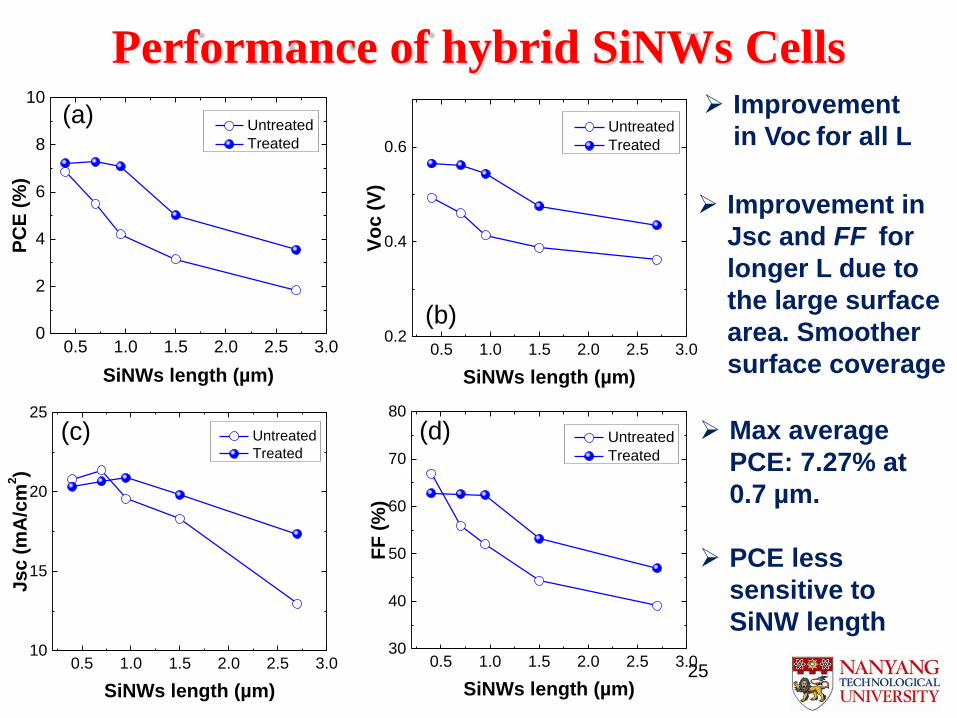
0.5 1.0 1.5 2.0 2.5 3.00.2
0.4
0.6
(b)
Vo
c (
V)
SiNWs length (µm)
Untreated
Treated
0.5 1.0 1.5 2.0 2.5 3.00
2
4
6
8
10
(a)
PC
E (
%)
SiNWs length (µm)
Untreated
Treated
0.5 1.0 1.5 2.0 2.5 3.030
40
50
60
70
80
(d)
FF
(%
)
SiNWs length (µm)
Untreated
Treated
0.5 1.0 1.5 2.0 2.5 3.010
15
20
25
(c)
Jsc (
mA
/cm
2)
SiNWs length (µm)
Untreated
Treated
Max average
PCE: 7.27% at
0.7 µm.
PCE less
sensitive to
SiNW length
Improvement
in Voc for all L
Improvement in
Jsc and FF for
longer L due to
the large surface
area. Smoother
surface coverage
Performance of hybrid SiNWs Cells
25
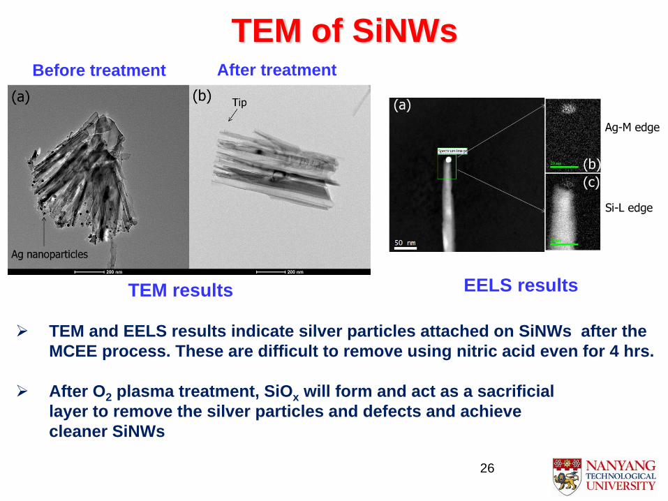
TEM of SiNWs
EELS results
TEM and EELS results indicate silver particles attached on SiNWs after the
MCEE process. These are difficult to remove using nitric acid even for 4 hrs.
After O2 plasma treatment, SiOx will form and act as a sacrificial
layer to remove the silver particles and defects and achieve
cleaner SiNWs
Before treatment After treatment
26
TEM results
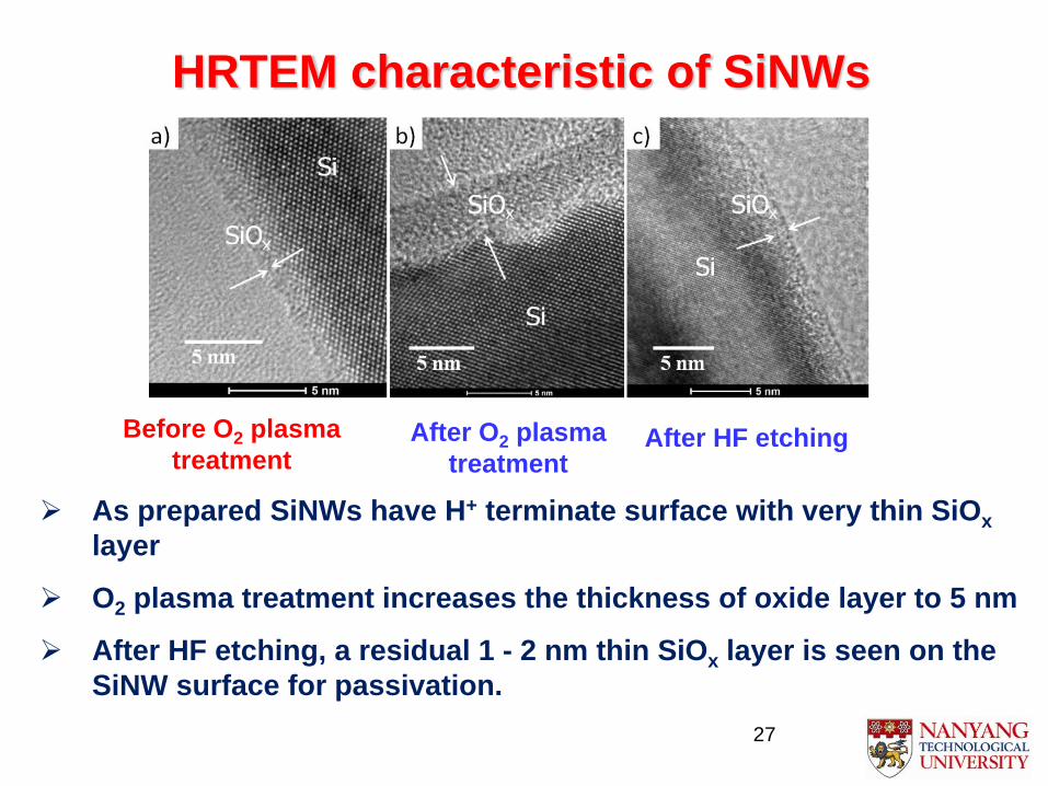
HRTEM characteristic of SiNWs
Before O2 plasma
treatment After O2 plasma
treatment After HF etching
As prepared SiNWs have H+ terminate surface with very thin SiOx
layer
O2 plasma treatment increases the thickness of oxide layer to 5 nm
After HF etching, a residual 1 - 2 nm thin SiOx layer is seen on the
SiNW surface for passivation.
27
Demonstrated a two-step surface treatment process to remove
residual impurities and defects near the SiNWs surface, and
effectively passivates the SiNWs to reduce the recombination
loss.
Treated SiNWs hybrid solar cell reveals a high PCE of 7.83%,
and the highest ever reported Voc of 0.572 V, for 0.7 µm SiNWs
based on a 10.6 µm thin Si film.
The proposed simple approach of surface treatment is
promising in boosting the efficiency of SiNW/organic hybrid cell
and will potentially lead to their practical use.
Conclusions
28

29