Embed Size (px)
Citation preview

Tampere University of Technology
Factors in Active Damping Design to Mitigate Grid Interactions in Three-Phase Grid-Connected Photovoltaic Inverters
CitationAapro, A. (2017). Factors in Active Damping Design to Mitigate Grid Interactions in Three-Phase Grid-Connected Photovoltaic Inverters. (Tampere University of Technology. Publication; Vol. 1502). TampereUniversity of Technology.Year2017
VersionPublisher's PDF (version of record)
Link to publicationTUTCRIS Portal (http://www.tut.fi/tutcris)
Take down policyIf you believe that this document breaches copyright, please contact [email protected], and we will remove access tothe work immediately and investigate your claim.
Download date:01.07.2018

Aapo AaproFactors in Active Damping Design to Mitigate GridInteractions in Three-Phase Grid-ConnectedPhotovoltaic Inverters
Julkaisu 1502 • Publication 1502
Tampere 2017
Tampereen teknillinen yliopisto. Julkaisu 1502 Tampere University of Technology. Publication 1502 Aapo Aapro Factors in Active Damping Design to Mitigate Grid Interactions in Three-Phase Grid-Connected Photovoltaic Inverters Thesis for the degree of Doctor of Science in Technology to be presented with due permission for public examination and criticism in Rakennustalo Building, Auditorium RG202, at Tampere University of Technology, on the 13th of October 2017, at 12 noon. Tampereen teknillinen yliopisto - Tampere University of Technology Tampere 2017

Doctoral candidate: Aapo Aapro
Laboratory of Electrical Energy Engineering Faculty of Computing and Electrical Engineering Tampere University of Technology Finland
Supervisor: Teuvo Suntio, Professor Laboratory of Electrical Energy Engineering Faculty of Computing and Electrical Engineering Tampere University of Technology Finland
Instructor: Tuomas Messo, Assistant professor Laboratory of Electrical Energy Engineering Faculty of Computing and Electrical Engineering Tampere University of Technology Finland
Pre-examiners: Xiongfei Wang, Associate professor Department of Energy Technology, Power Electronic Systems Faculty of Engineering and Science Aalborg University Denmark Pedro Luis Roncero Sánchez-Elipe, Associate professor School of Industrial Engineering University of Castilla-La Mancha Spain
Opponents: Xiongfei Wang, Associate professor Department of Energy Technology, Power Electronic Systems Faculty of Engineering and Science Aalborg University Denmark Marko Hinkkanen, Associate professor Department of Electrical Engineering and Automation School of Electrical Engineering Aalto University Finland
ISBN 978-952-15-4013-4 (printed) ISBN 978-952-15-4036-3 (PDF) ISSN 1459-2045

ABSTRACT
An LCL filter provides excellent mitigation capability of the switching frequency harmon-
ics, and is, therefore, widely used in grid-connected inverter applications. The resonant
behavior induced by the filter must be attenuated with passive or active damping meth-
ods in order to preserve the stability of the grid-connected converter. Active damping
can be implemented with different control algorithms, and it is frequently used due to
its relatively simple and low-cost implementation. However, active damping may easily
impose stability problems if it is poorly designed.
This thesis presents a comprehensive small-signal model of a three-phase grid-connected
photovoltaic inverter with LCL filter. The analysis is focused on a capacitor-current-
feedback (i.e., a multi-current feedback) active damping and its effects on the system
dynamics. Furthermore, a single-current-feedback active damping technique, which is
based on reduced number of measurements, is also studied. The main objective of this
thesis is to present an accurate multi-variable small-signal model for assessing the control
performance as well as the grid interaction sensitivity of grid-connected converters in the
frequency domain.
The state-of-the-art literature studies regarding the active damping are mainly con-
centrated on stability evaluation of the output-current loop, and the effect on external
characteristics such as susceptibility to background harmonics and impedance-based in-
stability has been overlooked. As the active damping affects significantly the sensitivity
to grid interactions, accurate predictions of the system transfer functions, e.g. the out-
put impedance, must be utilized in order to assess the active-damping-induced properties.
Moreover, the single-current-feedback active damping method lacks the aforementioned
analysis in the literature and, therefore, the need for accurate full-order small-signal
models is evident.
This thesis presents design criteria for the active damping in a wide range of operating
conditions. Accordingly, peculiarities regarding the active damping are discussed for both
multi and single-current-feedback active damping schemes. In addition, the parametric
influence of the active damping on the output-impedance characteristics is explicitly
analyzed. It is shown that the active damping design has a significant effect on the output
impedance and, therefore, the impedance characteristics should be considered in the
converter design for improved robustness against background harmonics and impedance-
based interactions.
iii


PREFACE
This research was carried out at the Laboratory of Electrical Energy Engineering (LEEE)
at Tampere University of Technology (TUT) during the years 2014 - 2017. The research
was funded by the university and ABB Oy. In addition, the financial support received
from the Finnish Academy of Science and Letters as well as from the Otto A. Malm
foundation is greatly appreciated.
First of all, I want to express my gratitude to Professor Teuvo Suntio for supervising
my thesis. All the constructive feedback as well as the insightful discussions have helped
and motivated me towards the degree. Moreover, my work would not be finished without
the contribution of other amazing members of our team. I want to thank especially
Assistant Professor Tuomas Messo for helping me throughout my academic career at the
university. All the discussions and your help with practical matters have contributed
a lot to my thesis work, and I appreciate it very much. Also, the current and former
members of our research team, Assistant Professor Petros Karamanakos, Ph.D. Jenni
Rekola, Ph.D. Juha Jokipii, M.Sc. Jukka Viinamaki, M.Sc. Jyri Kivimaki, M.Sc. Kari
Lappalainen, M.Sc. Julius Schnabel, M.Sc. Matti Marjanen, M.Sc. Markku Jarvela,
M.Sc. Matias Berg, B.Sc. Antti Hilden and B.Sc. Roosa-Maria Sallinen, you deserve a
special thanks for creating a delightful and relaxed atmosphere. Furthermore, all the staff
at LEEE deserve my thanks for making these years at the university extremely pleasant.
I am grateful to Associate Professors Xiongfei Wang and Pedro Roncero for examining
my thesis and providing supportive comments, which have helped me to improve the
quality of my thesis.
Last but not least, I want express my gratitude to my family, friends and Susanna. You
have supported and encouraged me throughout my academic career which has motivated
me more than I dare to admit. I thank you all for that.
Tampere, September 13, 2017
Aapo Aapro
v


CONTENTS
Abstract . . . . . . . . . . . . . . . . . . . . . . . . . . . . . . . . . . . . . . iii
Preface . . . . . . . . . . . . . . . . . . . . . . . . . . . . . . . . . . . . . . . v
Contents . . . . . . . . . . . . . . . . . . . . . . . . . . . . . . . . . . . . . . vii
Symbols and Abbreviations . . . . . . . . . . . . . . . . . . . . . . . . . . . ix
1. Introduction . . . . . . . . . . . . . . . . . . . . . . . . . . . . . . . . . . 1
1.1 Renewable energy and introduction to photovoltaic systems . . . . . . . . . 1
1.2 Small-signal modeling principles . . . . . . . . . . . . . . . . . . . . . . . . 4
1.3 Passive and active damping of LCL-filter resonance . . . . . . . . . . . . . 7
1.3.1 LCL-filter . . . . . . . . . . . . . . . . . . . . . . . . . . . . . . . . . . 7
1.3.2 Resonance damping . . . . . . . . . . . . . . . . . . . . . . . . . . . . . 8
1.3.3 Effect of delay on active damping . . . . . . . . . . . . . . . . . . . . . 9
1.3.4 Single-current-feedback active damping . . . . . . . . . . . . . . . . . . 10
1.4 Impedance-based analysis . . . . . . . . . . . . . . . . . . . . . . . . . . . . 11
1.5 Objectives and scientific contributions . . . . . . . . . . . . . . . . . . . . . 14
1.6 Related publications and author’s contribution . . . . . . . . . . . . . . . . 15
1.7 Structure of the thesis . . . . . . . . . . . . . . . . . . . . . . . . . . . . . . 16
2. Small-signal modeling of a three-phase grid-connected inverter . . . . 17
2.1 Average model . . . . . . . . . . . . . . . . . . . . . . . . . . . . . . . . . . 18
2.2 Operating point . . . . . . . . . . . . . . . . . . . . . . . . . . . . . . . . . 22
2.3 Linearized model . . . . . . . . . . . . . . . . . . . . . . . . . . . . . . . . . 24
2.4 Source-affected model . . . . . . . . . . . . . . . . . . . . . . . . . . . . . . 30
2.5 Load-affected model . . . . . . . . . . . . . . . . . . . . . . . . . . . . . . . 32
3. Active-damping-affected closed-loop model . . . . . . . . . . . . . . . . 35
3.1 Active damping considerations . . . . . . . . . . . . . . . . . . . . . . . . . 35
3.1.1 Active damping feedback coefficient . . . . . . . . . . . . . . . . . . . . 36
3.1.2 Properties of delay . . . . . . . . . . . . . . . . . . . . . . . . . . . . . 38
3.2 Open-loop dynamics in case of multi-current-feedback scheme . . . . . . . . 41
3.3 Open-loop dynamics in case of single-current-feedback scheme . . . . . . . 45
3.4 Closed-loop dynamics . . . . . . . . . . . . . . . . . . . . . . . . . . . . . . 50
3.4.1 Output-current control . . . . . . . . . . . . . . . . . . . . . . . . . . . 50
3.4.2 Input-voltage control . . . . . . . . . . . . . . . . . . . . . . . . . . . . 55
3.5 Root locus analysis . . . . . . . . . . . . . . . . . . . . . . . . . . . . . . . 59
3.5.1 Mitigation of delay in active damping feedback . . . . . . . . . . . . . 60
3.5.2 Multi-current-feedback active damping scheme . . . . . . . . . . . . . . 62
vii

3.5.3 Single-current-feedback active damping scheme . . . . . . . . . . . . . 65
4. Output impedance with active damping . . . . . . . . . . . . . . . . . . 73
4.1 Output impedance analysis . . . . . . . . . . . . . . . . . . . . . . . . . . . 73
4.1.1 Multi-current feedback scheme . . . . . . . . . . . . . . . . . . . . . . . 73
4.1.2 Single-current-feedback scheme . . . . . . . . . . . . . . . . . . . . . . 79
4.2 Comparison of single and multi-current-feedback schemes . . . . . . . . . . 81
4.2.1 Magnitude of output admittance . . . . . . . . . . . . . . . . . . . . . 82
4.2.2 Passivity of output admittance . . . . . . . . . . . . . . . . . . . . . . 85
4.3 Conclusions . . . . . . . . . . . . . . . . . . . . . . . . . . . . . . . . . . . . 87
5. Experimental results . . . . . . . . . . . . . . . . . . . . . . . . . . . . . 91
5.1 Open-loop verifications . . . . . . . . . . . . . . . . . . . . . . . . . . . . . 92
5.2 Closed-loop verifications . . . . . . . . . . . . . . . . . . . . . . . . . . . . . 93
5.2.1 Input-voltage control design . . . . . . . . . . . . . . . . . . . . . . . . 94
5.2.2 Output impedance verification . . . . . . . . . . . . . . . . . . . . . . . 95
5.2.3 Stability of the active damping loop . . . . . . . . . . . . . . . . . . . . 101
5.3 Impedance-based analysis . . . . . . . . . . . . . . . . . . . . . . . . . . . . 103
5.3.1 Nyquist stability criterion . . . . . . . . . . . . . . . . . . . . . . . . . 103
5.3.2 Impedance-based instability and background harmonics . . . . . . . . 105
6. Conclusions . . . . . . . . . . . . . . . . . . . . . . . . . . . . . . . . . . . 109
6.1 Final conclusions . . . . . . . . . . . . . . . . . . . . . . . . . . . . . . . . . 109
6.2 Future research topics . . . . . . . . . . . . . . . . . . . . . . . . . . . . . . 111
References . . . . . . . . . . . . . . . . . . . . . . . . . . . . . . . . . . . . . 113
A. Matlab code for CF-VSI steady state calculation . . . . . . . . . . . . 123
B. Current controller parameters . . . . . . . . . . . . . . . . . . . . . . . 127
C. Experimental setup . . . . . . . . . . . . . . . . . . . . . . . . . . . . . . 129
viii
SYMBOLS AND ABBREVIATIONS
ABBREVIATIONS
AC Alternating current
AD Active damping
ADC Analog-to-digital converter
BPF Band-pass filter
CC Constant current, current controller
CV Constant voltage
CSI Current-source inverter
DAC Digital-to-analog converter
DC Direct current
DC-DC DC to DC converter
DC-AC DC to AC converter
Dr. Tech. Doctor of Technology
DSP Digital signal processor
FRA Frequency-response analyzer
GW Gigawatt
HPF High-pass filter
LHP Left-half of the complex plane
LPF Low-pass filter
MPP Maximum power point
MPPT Maximum power point tracker
p.u. Percent unit
PC Personal computer
PI Proportional-integral controller
PLL Phase-locked loop
PRBS Pseudo-random binary sequence
PV Photovoltaic
PVG Photovoltaic generator
RHP Right-half of the complex plane
SAS Solar array simulator
TW Terawatt
VC Voltage controller
VSI Voltage-source inverter
ix

GREEK CHARACTERS
〈iLα〉 Alpha-component of the inductor current
〈iLβ〉 Beta-component of the inductor current
xα Alpha-component of a space-vector
xβ Beta-component of a space-vector
ωs Angular frequency of the grid
θc Phase angle
LATIN CHARACTERS
A Diode ideality factor
A Coefficient matrix A of the state-space representation,
Connection point for phase A inductor
B Coefficient matrix B of the state-space representation,
Connection point for phase B inductor
C Coefficient matrix C of the state-space representation,
Connection point for phase C inductor
Cin Capacitance of the DC-link capacitor
C Capacitance of the three-phase output filter
d Differential operator, d-component in the synchronous frame
d Small-signal duty ratio of the DC-DC converter
d Duty ratio space-vector
ds Duty ratio space-vector in synchronous frame
da Duty ratio of the upper switch in phase A
db Duty ratio of the upper switch in phas B
dc Duty ratio of the upper switch in phase C
dd Direct component of the duty ratio space-vector
dd Small-signal d-component of the duty ratio space-vector
dq Quadrature component of the duty ratio space-vector
dq Small-signal q-component of the duty ratio space-vector
D Coefficient matrix D of the state space representation
Dd Steady-state d-component of the duty ratio
Dq Steady-state q-component of the duty ratio
G Transfer function matrix
GAD, GAD Active damping gain, active damping gain matrix
Gcc-d,Gcc-q Current controller transfer functions
Gci Control-to-input transfer function
Gco Control-to-output transfer function
Gdel, Gdel Delay transfer function, delay transfer matrix
x
Gio Input-to-output transfer function
Gse Voltage sensing gains
Gvc Voltage controller
ii=a,b,c Current of phase a, b or c
I0 Dark saturation current
iC Capacitor C1 current
iCin DC-link capacitor current
id Current of the diode in the one-diode model
iin Inverter input current
iin Small-signal DC-DC converter output/inverter input current
Iin Steady-state inverter input current
〈isL1〉 Inverter-side inductor current space-vector in synchronous frame
〈iL1〉 Inverter-side inductor current space-vector in stationary frame
iL1 Small-signal inverter-side inductor L1 current
iL1(a,b,c) Inductor L1(a,b,c) current
〈iL1(a,b,c)〉 Average inductor L1(a,b,c) current
〈isL2〉 Grid-side inductor current space-vector in synchronous frame
〈iL2〉 Grid-side inductor current space-vector in stationary frame
iL2 Small-signal grid-side inductor L2 current
iL2(a,b,c) Grid-side inductor L2(a,b,c) current
〈iL2(a,b,c)〉 Average inductor L2(a,b,c) current
〈iL(1,2)d〉 Average d-component of the inductor current space-vector
iL(1,2)d Small-signal d-component of the inductor current space-vector
IL(1,2)d Steady-state d-component of the inductor current
irefL1d Reference of the output current d-component
〈iL(1,2)q〉 Average q-component of the inductor current space-vector
iL(1,2)q Small-signal q-component of the inductor current space-vector
IL(1,2)q Steady-state q-component of the inductor current
irefL1q Reference of the output current q-component
io(a,b,c) Output phase current, refer to iL2(a,b,c)
〈io-d〉 Average d-component of the output current space-vector
iod Small-signal d-component of the output current space-vector
〈io-q〉 Average q-component of the output current space-vector
ioq Small-signal q-component of the output current space-vector
iP Current flowing from the DC-link toward the inverter switches
〈iP〉 Average current flowing toward the inverter switches
iph Photocurrent
ipv Small-signal output current of the photovoltaic generator
ipv Output current of the photovoltaic generator
Ipv Steady-state output current of the photovoltaic generator
xi
Isc Short-circuit current of the photovoltaic generator
j Imaginary part
ki Scaling constant of the integral term in PI-controller
kp Scaling constant of the proportional term in PI-controller
L Inductance of the inverter when all phases are symmetrical
L1(a,b,c) Inverter-side inductance of phase A/B/C
L2(a,b,c) Grid-side inductance of phase A/B/C
Lin DC-link voltage control loop gain
Lout-d Current control loop gain of the d-component
Lout-q Current control loop gain of the q-component
LPLL Control loop gain of the phase-locked-loop
n Neutral point
N Negative rail of the DC-link
P Positive rail of the DC-link
PMPP Power at the maximum-power point
ppv Instantaneous output power of the photovoltaic generator
q Q-component in the synchronous frame
rC Parasitic resistance of capacitor C
rCin Parasitic resistance of the DC-link capacitor
rD Parasitic resistance of a diode
Rd Damping resistance, virtual resistor value
Req Equivalent resistance related to the inverter
rL1(a,b,c) Parasitic resistance of inverter-side inductor L1
rL2(a,b,c) Parasitic resistance of grid-side inductor L2
rpv Dynamic resistance of the photovoltaic generator
rs Series resistance in the one-diode model
rsh Shunt resistance in the one-diode model
rsw Parasitic resistance of the converter switches
s Laplace variable
u Column-vector containing input variables
U Input-variable vector in Laplace-domain
ua Voltage of phase A
〈ua〉 Average voltage of phase A
〈uAN〉 Average voltage between points A and N
ub Voltage of phase B
〈ub〉 Average voltage of phase B
〈uBN〉 Average voltage between points B and N
uc Voltage of phase C
〈uc〉 Average voltage of phase C
〈uCN〉 Average voltage between points C and N
xii

〈usC〉 Filter capacitor voltage space-vector in synchronous frame
〈uC〉 Filter capacitor voltage space-vector in stationary frame
uC Small-signal voltage over the capacitor C
uC Voltage over the capacitor C
UC Steady-state voltage over the capacitor C
uCin DC-link capacitor voltage
uCin Small-signal DC-link capacitor voltage
UCin Steady-state DC-link capacitor voltage
ui=a,b,c Three-phase grid voltages
ud Voltage over a diode in the one-diode model
〈ug〉 Grid voltage space-vector
〈usg〉 Grid voltage space-vector in synchronous frame
uin Small-signal input voltage
〈uin〉 Average input voltage
uin Instantaneous input voltage
Uin Steady-state input voltage
〈uL〉 Inductor voltage space-vector
uL(a,b,c) Voltage over the inductor La,b,c
〈uL(a,b,c)〉 Average voltage over the inductor La,b,c
UMPP Voltage at the maximum power point
〈unN〉 Average common-mode voltage
uo Output voltage
Uoc Open-circuit voltage of the photovoltaic generator
Uod Steady-state d-component of the grid voltage
uod Small-signal d-component of the grid voltage
Uoq Steady-state q-component of the grid voltage
uoq Small-signal q-component of the grid voltage
upv Voltage across the photovoltaic generator terminals
Upv Steady-state voltage of the photovoltaic generator
t Time
Toi Open-loop output-to-input transfer function
x Vector containing state variables
x Space-vector
xs Space-vector in a synchronous reference frame
x0 Zero component of a space-vector
xa Variable related to phase A
xb Variable related to phase B
xc Variable related to phase C
xd Direct component of a space-vector
xq Quadrature component of a space-vector
xiii

y Vector containing output variables
Y Output-variable vector in Laplace-domain
Yo Output admittance
Zin Input impedance
Zo Output impedance
SUBSCRIPTS
d Transfer function related to d-components
dq Transfer function from d to q-component
f Variable related to the three-phase filter
mod Active-damping-related modifier transfer function
q Transfer function related to q-components
qd Transfer function from q to d-component
sw Power electronic switch
SUPERSCRIPTS
∗ Complex conjugate of a space-vector
-1 Inverse of a matrix or a transfer function
AD Transfer function which includes the effect of active damping
c Variable in the control system reference frame
DC-DC Transfer function related to the DC-DC converter
DC-AC Transfer function related to the inverter
g Variable in the grid reference frame
L Transfer function which includes the effect of the load
multi Transfer function related to multi-current-feedback active damping
out Transfer function which includes the effect of the current control
ref Reference value
single Transfer function related to single-current-feedback active damping
S Transfer function which includes the effect of the source
tot Transfer function which includes the effect of the voltage control
xiv

1 INTRODUCTION
This chapter discusses the background of the thesis and introduces the reader to the topic.
Accordingly, an introduction for photovoltaic energy systems is given first and the details
regarding the behavior of photovoltaic generators as energy sources are elaborated. Small-
signal modeling is applied extensively in this thesis and, therefore, the background for
the modeling method as well as its usefulness are highlighted. Theory behind the active
damping and output impedance analysis are also discussed as they form the framework
for the thesis.
1.1 Renewable energy and introduction to photovoltaic systems
Evidence for global warming and the greenhouse effect is undeniable. Globally, approx-
imately 87% of the total energy produced is generated by fossil fuels from which the
majority (38%) comes from oil [1]. Excessive use of fossil fuels increases the emissions
of carbon dioxide (CO2) which, in turn, further accelerates the greenhouse effect. In
order to slow down the climate change, public attention has been drawn on the issue
and, correspondingly, European Union has launched the Roadmap 2050-project with an
objective to reduce greenhouse gas emissions at least 80% below the 1990 levels by 2050
[2]. Fossil fuel-dependency must be decreased in order to stop accumulating CO2 into
the atmosphere and, thus, these actions are highly necessary.
The aforementioned factors have led to growing interest in the field of grid-connected
renewable energy systems, and the utilization of these has been increasing continuously
for several years [1]. Solar energy is one of the most promising renewable energy resources
due to its environmentally friendly features and relatively low cost of harvesting. Fur-
thermore, it is practically inexhaustible within a realistic time frame. Energy from the
Sun is mainly harvested either by using it for heating or by converting to electrical en-
ergy. Usually, the electrical energy is harvested using silicon-based solar panels and their
price has been rapidly decreasing throughout the world, which makes the use of them in
energy production feasible in terms of invested money and payback time. Regarding the
usability of solar energy, it is expected to be the second most utilized energy source by
2020 excluding hydroelectric energy [3].
Considering the electrical characteristics, the photovoltaic generators produce direct
current (DC), which has to be transformed into alternating current (AC) in order to
1
Chapter 1. Introduction
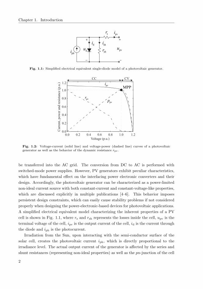
Fig. 1.1: Simplified electrical equivalent single-diode model of a photovoltaic generator.
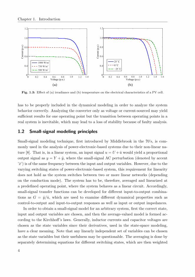
Fig. 1.2: Voltage-current (solid line) and voltage-power (dashed line) curves of a photovoltaicgenerator as well as the behavior of the dynamic resistance rpv.
be transferred into the AC grid. The conversion from DC to AC is performed with
switched-mode power supplies. However, PV generators exhibit peculiar characteristics,
which have fundamental effect on the interfacing power electronic converters and their
design. Accordingly, the photovoltaic generator can be characterized as a power-limited
non-ideal current source with both constant-current and constant-voltage-like properties,
which are discussed explicitly in multiple publications [4–6]. This behavior imposes
persistent design constraints, which can easily cause stability problems if not considered
properly when designing the power-electronic-based devices for photovoltaic applications.
A simplified electrical equivalent model characterizing the inherent properties of a PV
cell is shown in Fig. 1.1, where rs and rsh represents the losses inside the cell, upv is the
terminal voltage of the cell, ipv is the output current of the cell, id is the current through
the diode and iph is the photocurrent.
Irradiation from the Sun, upon interacting with the semi-conductor surface of the
solar cell, creates the photovoltaic current iph, which is directly proportional to the
irradiance level. The actual output current of the generator is affected by the series and
shunt resistances (representing non-ideal properties) as well as the pn-junction of the cell
2

1.1. Renewable energy and introduction to photovoltaic systems
which can be presented as
ipv = iph − i0(e
upv+rsipvNakT/q − 1
)︸ ︷︷ ︸
id
−upv + rsipv
rsh, (1.1)
where i0 is the diode reverse saturation current, T (Kelvin) is the cell temperature, k is
the Bolzmann constant, a the diode ideality factor, q the electron charge and N is the
number of series-connected photovoltaic cells.
As can be deduced from the exponential term in (1.1), the voltage-current characteris-
tics of the PV cell are highly non-linear and can be conveniently solved only by numerical
methods. Accordingly, the illustration of the voltage-current and voltage-power depen-
dency of a traditional PV cell can be given as shown in Fig. 1.2. Maximum power can be
extracted only at one point, which is called the maximum power point (MPP), although,
recent literature indicates that it is in practice a wider constant power region (CPR) [7].
The control system of the interfacing converter tries to keep the operating point near the
MPP for maximal power extraction.
Considering Eq. (1.1) as well as Figs. 1.3a and 1.3b, the electrical characteristics of
the PV cell will change in proportion to the irradiance level and the cell temperature.
Evidently, the short-circuit current produced by the PV cell is directly proportional to
the irradiance and, conversely, only minor changes in the open-circuit voltage of the PV
cell can be observed when the irradiation level changes. The temperature of the PV cell,
on the other hand, affects mainly the open-circuit voltage and has negligible effect on
the short-circuit current. Accordingly, higher open-circuit voltages are obtained when
the cell temperature is lower, thus an increase of the cell temperature decreases the
maximum power extractable from the cell. Consequently, based on the aforementioned
factors, the PV current has relatively fast dynamics, affected mainly by the irradiance
level, compared to the voltage, which has only slow temperature-dependent dynamics.
In addition to the MPP, two distinct operating regions can be observed in the PV-
cell current-voltage (IV) behavior according to Fig. 1.2. When the voltage of the PV
cell is below the MPP voltage, a constant current region (CCR) is found, where the
current remains relatively constant despite the changes in the PV cell voltage and the
PV cell exhibits higher dynamic resistance, thus resembling the characteristics of an
ideal current source. Conversely, when the cell voltage is above the MPP voltage, the
behavior of the PV cell resembles a constant voltage source as the dynamic resistance of
the converter is small and the voltage stays relatively constant regardless of the changes
in the current. Correspondingly, this is called the constant voltage region (CVR). Due to
the aforementioned constant-voltage and constant-current-like properties, the design and
control of the inverter have inherent constraints and, therefore, the effect of the source
3
Chapter 1. Introduction
(a) (b)
Fig. 1.3: Effect of (a) irradiance and (b) temperature on the electrical characteristics of a PV cell.
has to be properly included in the dynamical modeling in order to analyze the system
behavior correctly. Analyzing the converter only as voltage or current-sourced may yield
sufficient results for one operating point but the transition between operating points in a
real system is inevitable, which may lead to a loss of stability because of faulty analysis.
1.2 Small-signal modeling principles
Small-signal modeling technique, first introduced by Middlebrook in the 70’s, is com-
monly used in the analysis of power-electronic-based systems due to their non-linear na-
ture [8]. That is, in a linear system, an input signal u = U+ u would yield a proportional
output signal as y = Y + y, where the small-signal AC perturbation (denoted by accent
’x’) is of the same frequency between the input and output variables. However, due to the
varying switching states of power-electronic-based system, this requirement for linearity
does not hold as the system switches between two or more linear networks (depending
on the conduction mode). The system has to be, therefore, averaged and linearized at
a predefined operating point, where the system behaves as a linear circuit. Accordingly,
small-signal transfer functions can be developed for different input-to-output combina-
tions as G = y/u, which are used to examine different dynamical properties such as
control-to-output and input-to-output responses as well as input or output impedances.
In order to obtain a small-signal model for an arbitrary system, first the correct state,
input and output variables are chosen, and then the average-valued model is formed ac-
cording to the Kirchhoff’s laws. Generally, inductor currents and capacitor voltages are
chosen as the state variables since their derivatives, used in the state-space modeling,
have a clear meaning. Note that any linearly independent set of variables can be chosen
as the state variables but their usefulness may be questionable. The averaging is done by
separately determining equations for different switching states, which are then weighted
4

1.2. Small-signal modeling principles
(averaged) over one switching cycle to remove the effect of the switching ripple. Accord-
ingly, the average-valued or the large-signal model is obtained and the corresponding
state-space equations can be given by
dxdt = Ax+ Bu
y = Cx+ Du(1.2)
where vectors x, u and y denote the state, input and output variable vectors, respectively.
This may not be sufficient for the formulation of the system transfer functions because
such model may be nonlinear after recognizing the duty ratio (or the control signal) d as a
modulated variable and, therefore, an input signal [8]. Correspondingly, a situation may
arise where the state or output variables are multiplied by the duty ratio, which yields a
nonlinear dependency between the variables. Therefore, in that case, the system has to be
linearized by taking partial derivatives of each variable, which removes the corresponding
nonlinearity. After linearizing the equations, the system model can be represented by a
linearized state-space in the Laplace-domain as shown in (1.3), from which the system
transfer functions can be derived as in (1.4). This small-signal modeling technique is
further elaborated in Chapter 2 for a specific application, i.e. for a three-phase grid-
connected PV inverter.
dxdt = Ax+ Bu
y = Cx+ Du→
sx = Ax+ Bu
y = Cx+ Du(1.3)
y(s) =[C(sI−A)
−1B + D
]u = Gu(s) (1.4)
Depending on the terminal constraints, i.e., the inherent behavior of the source and
load as well as the selection of the feedback variables, an appropriate conversion scheme
must be chosen for the analysis. Accordingly, four different conversion schemes are shown
in Figs. 1.4a-1.4d.
As discussed earlier, the photovoltaic generator exhibits characteristics of a non-linear
current source, thus, a current source is a convenient selection as an input source, i.e.,
the cases shown in Figs. 1.4b or 1.4d. Furthermore, due to rather slow dynamics of the
PV voltage (affected mainly by the temperature), the input voltage can be conveniently
controlled for maximum power extraction, which complies with the selection of the input
source. Considering the output terminal, in grid-connected applications, the output
voltage is determined by the external system (i.e. the grid). A stiff grid is, therefore,
5

Chapter 1. Introduction
(a) (b)
(c) (d)
Fig. 1.4: Depiction of a) voltage-to-voltage, b) current-to-current, c) voltage-to-current and d)current-to-voltage conversion schemes.
assumed in this case, which leads to a conclusion that only the H-parameter (current-to-
current conversion scheme) model is applicable in the analysis. Accordingly, the input
source of the converter is a current source and the input voltage is the input-side feedback
variable in order to guarantee maximum power output by means of the MPP tracking
(MPPT). Furthermore, the converter output is loaded by a stiff voltage source and the
system controls its output current (current injection-mode), which is known as a grid-
parallel or grid-feeding mode.
Modeling of three-phase converters differs from the modeling of DC-DC converters,
since the space-vector theory has to be used to analyze the three-phase variables. This
means that the inverter is not analyzed per phase, but instead the three-phase variables
of the small-signal model are transformed into synchronous (dq-domain) or stationary
reference (αβ-domain) frames. Many publications analyze the inverter in a stationary
reference frame in order to decrease the complexity of the analysis and the computational
burden as discussed, for example, in [9–13]. However, some inconsistencies arise, since
in a stationary reference frame the steady-state operating point cannot be solved in a
consistent manner, which imposes restrictions for the small-signal modeling requiring a
steady-state operating point. In the rotating or synchronous reference frame, the AC-
quantities appear constant (i.e., DC) in the steady state, which allows the linearizing of
the system.
6

1.3. Passive and active damping of LCL-filter resonance
(a) (b)
Fig. 1.5: Depictions of (a) L-filtered and (b) LCL-filtered grid-connected converters.
1.3 Passive and active damping of LCL-filter resonance
1.3.1 LCL-filter
In grid-connected applications, an inductive (L-type) filter may not sufficiently attenuate
the switching-ripple currents. High power applications produce larger currents, which
require high value for inductance in order to obtain sufficient attenuation of the switching
harmonics. This naturally increases the system costs and size. Therefore, inductive-
capacitive-inductive (LCL) filters have gained popularity as filtering elements due to their
excellent harmonic attenuation capability also at lower switching frequencies [14]. An
LCL-filter enables wide range of power levels with relatively small values for inductances
and capacitance to achieve the same filtering performance as with only an L-type filter
[10, 14–20]. For demonstrative purposes, the two filtering topologies are shown in Figs.
1.5a and 1.5b. Inherently, the LCL-filter creates several resonances in the dq-domain
control dynamics of the converter, which must be damped in order to ensure robust
performance and stability of the converter. The resonant frequencies are dependent on
the passive component values of the filter and can be generally given as
ωres =
√L1 + L2
L1L2C, (1.5)
ω0 =
√1
L2C. (1.6)
The resonance given in (1.5) is caused by the series-parallel interaction of inverter-side
inductance as well as the grid-side inductance and capacitance. Respectively, the other
resonance in (1.6) is caused by the series interaction between the grid-side inductance L2
and the filter capacitance C.
7

Chapter 1. Introduction
(a)
(b)
Fig. 1.6: Simplified block diagram of a control system with (a) filter-based and (b) multi-loopactive damping methods.
1.3.2 Resonance damping
The resonant behavior induced by the LCL-filter can be attenuated with passive or active
damping methods [14, 15, 20]. The most elementary method to damp the resonance is to
add a resistor in series with the LCL-filter capacitor, which is commonly known as passive
damping. Note that the resistor can be placed in parallel or series with all the passive
filtering components in order to damp the resonances. The series damping resistor with
the filter capacitor can be still considered as the most popular technique in the literature.
Although, the resistor provides desired resonance damping, it also causes reduction in
the attenuation capability and ohmic losses reducing the converter efficiency by up to
1 %. [15]. Moreover, the system costs are increased due to additional components and
possible cooling elements (especially in high-power applications).
Active damping, on the other hand, is performed with different control algorithms,
which are used to attenuate the resonant behavior and, due to the absence of resistive
elements (excluding the ESRs of the components), power losses are negligible in the filter
[21, 22]. Moreover, the attenuation capability of the filter is unaffected. Generally, active
damping can be implemented either as a filter-based or multi-loop-based method, which
are depicted in Figs. 1.6a and 1.6b, respectively.
Considering the filter-based method illustrated in Fig. 1.6a, no additional feedback
loop is added due to the active damping. Basically, the active damping is performed by
modifying the inverter control signal (or duty ratio) by means of digital filters such as
low-pass, lead-lag or notch filters. Accordingly, the purpose of this method is to induce
counter-resonance at the corresponding LCL-filter resonant frequencies in order to guar-
antee stable operation [23, 24]. This makes the filter-based active damping extremely
8

1.3. Passive and active damping of LCL-filter resonance
cost-efficient since no additional sensors are needed. As the filter-based methods usually
utilize parameters from the physical filter and their implementation may be fixed inside
the control system (excluding adaptive filters in special cases [25]), corresponding active
damping methods are prone to inaccuracy and may even exhibit inferior stability char-
acteristics due to parameter variation caused, e.g., by grid inductance and component
aging.
Multi-loop active damping methods include additional feedbacks from a system state
variable, which is used to modify the inverter control signal [20, 26, 27] or the inverter
output current reference [22] (cf. Fig. 1.6b). However, in the latter case, the bandwidth of
the current control limits the performance of the active damping. Considering convenient
feedback variables for active damping, the filter capacitor current is usually adopted as
a state feedback [27–33]. The filter capacitor voltage is also a common feedback variable
[21, 31], although, problems may occur due to the discrete realization of derivative-
operator (i.e., iC = CduC/dt) inside the control system [31]. If a current-feedback is
utilized, the aforementioned feedback signal is used to create a so-called virtual resistor,
which provides the resonance damping by emulating the effect of a passive resistor in
series with the filter capacitor inside the control system dynamics [22, 27, 28]. Regarding
the naming of the aforementioned concept, the virtual resistor is a convenient term for
industrial designers due to its correspondence to the physical entity. However, it is
inherently a control loop and should not be considered other than a multi-loop active
damping method during the control design. Due to the factors discussed above and the
popularity of the capacitor-current-feedback active damping technique, it is analyzed in
this thesis.
1.3.3 Effect of delay on active damping
Digital processing delay, present in modern digital control systems, deteriorates the per-
formance of active damping. That is, the active damping feedback signal may be modified
significantly by the delay causing insufficient damping or stability problems due to the
appearance of right-half-plane (RHP) poles in the output-current-control dynamics [28–
30, 34–38]. The delay nearly exclusively determines the performance and stability of
active damping as well as it imposes major design constraints. Accordingly, the condi-
tion where the resonant frequency (cf. Eq. (1.5)) of the LCL-filter equals one-sixth of the
sampling frequency (fs) has been observed to be critical for stability of a grid-connected
converter [28, 29, 31, 34, 35, 37, 39, 40]. Accordingly, the active damping feedback has
to be modified depending on the resonant frequency of the LCL-filter and the sampling
frequency of the control system in order to avoid delay-induced RHP-poles in the control
loop.
The system delay can either induce improved or inferior stability characteristics de-
9
Chapter 1. Introduction
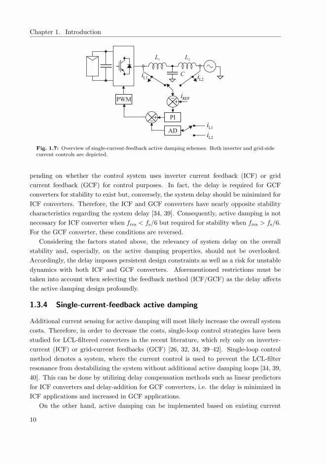
Fig. 1.7: Overview of single-current-feedback active damping schemes. Both inverter and grid-sidecurrent controls are depicted.
pending on whether the control system uses inverter current feedback (ICF) or grid
current feedback (GCF) for control purposes. In fact, the delay is required for GCF
converters for stability to exist but, conversely, the system delay should be minimized for
ICF converters. Therefore, the ICF and GCF converters have nearly opposite stability
characteristics regarding the system delay [34, 39]. Consequently, active damping is not
necessary for ICF converter when fres < fs/6 but required for stability when fres > fs/6.
For the GCF converter, these conditions are reversed.
Considering the factors stated above, the relevancy of system delay on the overall
stability and, especially, on the active damping properties, should not be overlooked.
Accordingly, the delay imposes persistent design constraints as well as a risk for unstable
dynamics with both ICF and GCF converters. Aforementioned restrictions must be
taken into account when selecting the feedback method (ICF/GCF) as the delay affects
the active damping design profoundly.
1.3.4 Single-current-feedback active damping
Additional current sensing for active damping will most likely increase the overall system
costs. Therefore, in order to decrease the costs, single-loop control strategies have been
studied for LCL-filtered converters in the recent literature, which rely only on inverter-
current (ICF) or grid-current feedbacks (GCF) [26, 32, 34, 39–42]. Single-loop control
method denotes a system, where the current control is used to prevent the LCL-filter
resonance from destabilizing the system without additional active damping loops [34, 39,
40]. This can be done by utilizing delay compensation methods such as linear predictors
for ICF converters and delay-addition for GCF converters, i.e. the delay is minimized in
ICF applications and increased in GCF applications.
On the other hand, active damping can be implemented based on existing current
10

1.4. Impedance-based analysis
measurements in the single-loop control scheme, i.e., an additional loop is formed from
the measured inverter or grid currents. For convenience, the single-current-feedback term
denotes here that the existing current measurements in the single-loop scheme are also
used for active damping. Corresponding methods have been successfully demonstrated
e.g. in [32, 36, 43, 44]. The additional loop distinguishes the conventional pure single-loop
methods from the modified single-current-feedback active damping methods. In order to
illustrate the topic further, Fig. 1.7 presents the simplified block diagram of the modified
single-loop control schemes.
Considering the stability and robustness, different conclusions have been made re-
garding, which of the single-current-feedback methods - ICF or GCF system - is the
best. Reference [32] concludes that the ICF method would be superior due to inherent
damping effect of the aforementioned control solution. However, the effect of system
delay is neglected in the analysis, which hides essential inherent properties of active
damping [34]. Single-current-feedback active damping was also proposed to be successful
for ICF converters in [43]. Conversely, the GCF system might be more convenient as
the system delay, persistent in digitally controlled systems, is beneficial for its stability
contrary to the ICF systems [34, 39]. Successful control system and active damping
implementations have been proposed for both ICF and GCF converters and no clear
consensus can be found whether one of the aforementioned method is superior over the
other [32, 36, 43, 44]. Therefore, the system dynamics of an ICF converter are further
elaborated in this thesis in order to widen the knowledge for corresponding converters.
The single-current-feedback scheme is inherently different from its capacitor-current-
feedback counterpart and, therefore, different dynamic properties are naturally imposed
in the converter dynamics. The differences between the aforementioned two schemes need
to be highlighted in order to further improve the knowledge on single-current-feedback
active damping methods.
1.4 Impedance-based analysis
Considering the output terminal properties of a power electronic converter, a small-signal
response between the voltage and current at the same terminal represents an admittance
or impedance depending on the system configuration. In a grid-feeding converter (i.e.,
the output terminal current is controlled), the relation between the voltage and cur-
rent is considered as admittance, which represents the frequency-domain response of the
output current against output voltage perturbations. Conversely, for a grid-forming con-
verter (i.e., the output terminal voltage is controlled), the output impedance represents
the response of output voltage against the grid-current perturbations. Accordingly, the
responses can be expressed as Yo = io/uo and Zo = uo/io for the grid-feeding and grid-
forming converters, respectively. However, regarding the topic of the thesis, only the
11
Chapter 1. Introduction
former is considered.
Active damping affects the system dynamics (i.e., transfer functions) by modifying
the duty ratio of the converter and, thus, introducing an additional loop-structure inside
the output-current-control loop. As the output-current loop affects the deviations be-
tween the measured and reference currents only within its bandwidth, the effect of active
damping is visible at frequencies beyond the output-current loop. Thus, different output
impedance properties are obtained at the resonant frequency, which dictate the external
behavior of the converter, i.e., the susceptibility to the grid background harmonics and
harmonic instability.
The utility grid usually contains numerous power electronic devices as well as other
non-linear loads, which draw non-sinusoidal currents. Consequently, the current consists
of multiple harmonics, which interact with the grid impedance causing distortions in the
supply voltage waveform. The grid impedance is determined by the configuration of the
power delivery system including transmission cables, transformers and other power elec-
tronic devices. These affect the grid impedance seen by grid-connected electrical systems
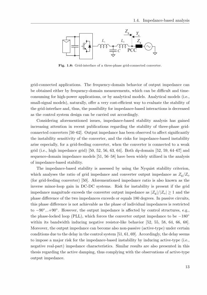
as illustrated in Fig. 1.8. Accordingly, the grid impedance at the point-of-common-
coupling (PCC) may contain several resonances along with the inductive characteristics
at higher frequencies, which makes the grid impedance estimation a challenging task
[45, 46].
If the grid voltage contains harmonics at a certain frequency, the operation of grid-
connected power-electronic converters can be disturbed. Accordingly, the injected current
(in grid-feeding converters) at the output terminal is affected according to the Ohm’s
law as io = uo/Zo and, therefore, high output impedance prevents the grid-voltage
harmonics from affecting the grid current. Considering active damping and the high-
frequency impedance behavior, high output impedance is required especially in multi-
parallel inverter systems, where inverters can interact with each other and cause the
point-of-common coupling (PCC) voltage to oscillate [47, 48]. Low output impedance
allows such oscillations to be transferred into the grid current, which can further enhance
the PCC voltage distortions via the grid impedance.
Grid current oscillations may occur also without significant grid background har-
monics. This is caused by the finite grid impedance, which interacts with the output
impedance of the converter, i.e., impedance-based interactions occur. Harmonic insta-
bilities and resonances in solar power plants have revealed that such interactions may
cause severe damage to the system hardware and impair the power quality in the grid
[49]. These power quality problems, however, are not purely dependent on the internal
stability of interconnected converters, and their stable control systems do not necessar-
ily guarantee absence of harmonic resonances. Therefore, accurate output impedance
models are essential when predicting the possibility for impedance-based interactions in
12
1.4. Impedance-based analysis
Fig. 1.8: Grid-interface of a three-phase grid-connected converter.
grid-connected applications. The frequency-domain behavior of output impedance can
be obtained either by frequency-domain measurements, which can be difficult and time-
consuming for high-power applications, or by analytical models. Analytical models (i.e.,
small-signal models), naturally, offer a very cost-efficient way to evaluate the stability of
the grid-interface and, thus, the possibility for impedance-based interactions is decreased
as the control system design can be carried out accordingly.
Considering aforementioned issues, impedance-based stability analysis has gained
increasing attention in recent publications regarding the stability of three-phase grid-
connected converters [50–62]. Output impedance has been observed to affect significantly
the instability sensitivity of the converter, and the risks for impedance-based instability
arise especially, for a grid-feeding converter, when the converter is connected to a weak
grid (i.e., high impedance grid) [50, 52, 56, 63, 64]. Both dq-domain [52, 59, 64–67] and
sequence-domain impedance models [51, 56–58] have been widely utilized in the analysis
of impedance-based stability.
The impedance-based stability is assessed by using the Nyquist stability criterion,
which analyses the ratio of grid impedance and converter output impedance as Zg/Zo
(for grid-feeding converter) [50]. Aforementioned impedance ratio is also known as the
inverse minor-loop gain in DC-DC systems. Risk for instability is present if the grid
impedance magnitude exceeds the converter output impedance as |Zg|/|Zo| ≥ 1 and the
phase difference of the two impedances exceeds or equals 180 degrees. In passive circuits,
this phase difference is not achievable as the phase of individual impedances is restricted
to −90...+90. However, the output impedance is affected by control structures, e.g.,
the phase-locked loop (PLL), which forces the converter output impedance to be −180
within its bandwidth inducing negative resistor-like behavior [52, 55, 58, 64, 66, 68].
Moreover, the output impedance can become also non-passive (active-type) under certain
conditions due to the delay in the control system [51, 61, 69]. Accordingly, the delay seems
to impose a major risk for the impedance-based instability by inducing active-type (i.e.,
negative real-part) impedance characteristics. Similar results are also presented in this
thesis regarding the active damping, thus complying with the observations of active-type
output impedance.
13
Chapter 1. Introduction
Even though active damping affects the output impedance significantly, there is no
explicit analysis in the literature considering the issue, and some publications have only
briefly discussed the topic. For example, passivity-based stability and impedance analysis
for power electronic converters with active damping were discussed in [18, 63, 65, 70–
73], but the comprehensive parametric influence of the active damping on the output
impedance was not analyzed nor the actual impedances are experimentally verified in
[18, 65, 70, 71, 73]. Output impedance analysis with active damping was presented
briefly for GCF converters in [74], but the effect of the delay was neglected, which hides
important information regarding the ratio of LCL-filter resonant and sampling frequen-
cies. Furthermore, the impedances were not verified experimentally in the aforementioned
paper. Active damping of DC-DC converters and its impedance properties were analyzed
in [75], but the results are not directly applicable for DC-AC grid-connected converters
with LCL-filters.
Clearly, the effect of the traditional capacitor-current-feedback active damping on the
output impedance needs to be further clarified considering the lack of explicit analysis on
the topic. Furthermore, as the single-current-feedback active damping scheme provides
an attractive alternative due to its simple and inexpensive implementation, the single-
current-feedback scheme and its output impedance properties are analyzed and compared
to the multi-current counterpart. Due to the absence of proper research on the topic, this
thesis provides incremental knowledge on the multi and single-current-feedback schemes.
Severe impedance-based stability problems and harmonic resonances can be avoided if
proper impedance modification via active damping is performed as will be discussed in
this thesis.
1.5 Objectives and scientific contributions
This thesis presents a comprehensive small-signal model of a grid-connected PV inverter
with active damping using multi-variable small-signal modeling technique. Accurate pre-
dictions of inverter transfer functions are obtained, which are utilized to elaborate the
active-damping-induced properties on the output impedance and overall system dynam-
ics. Furthermore, the stability criteria for the active damping are studied for LCL-filter
resonant frequencies both lower and higher than the critical frequency of fs/6 with multi-
current as well as single-current-feedback schemes. Accordingly, active damping design
criteria are presented and clarified for ICF converters by using both root trajectory and
frequency-domain analysis. In addition, the parametric influence of the active damping
on the output impedance characteristics is explicitly analyzed. It is shown that the ac-
tive damping design has a significant effect on the output impedance and, therefore, the
impedance analysis should be utilized in the converter design for improved robustness
against background harmonics and impedance-based interactions.
14

1.6. Related publications and author’s contribution
The scientific contribution of this thesis can be summarized as follows:
• An accurate small-signal model characterizing the open and closed-loop dynamics
of a three-phase grid-connected PV inverter with LCL-filter is formulated in this
thesis. So far, explicit small-signal models for the corresponding inverter topology
do not exist in the literature.
• Active damping and its effect on the system dynamics are analyzed by utilizing
multi-variable modeling method, which is a novel way to study active damping.
This allows explicit and accurate analysis of active damping on the system dy-
namics and it significantly simplifies the model derivation, which can be done with
comparable effort to simple DC-DC converters.
• Output impedance characteristics for the capacitor-current-feedback active damp-
ing are presented for the first time in literature. This introduces a useful method
to further improve the active damping design, which usually concentrates on the
stability evaluation of the output-current control. Accordingly, the external char-
acteristics of the inverter can be conveniently analyzed and, thus, the robustness
against harmonic instability can be improved.
• Single-current-feedback active damping and its impedance properties are presented
and, therefore, important information regarding the differences between the multi-
current and single-current-feedback schemes are obtained.
1.6 Related publications and author’s contribution
The following publications form the basis of this thesis.
[P1] Aapro, A., Messo, T., Roinila, T. and Suntio, T. (2017). “Effect of active damping on
output impedance of three-phase grid-connected converter”, in IEEE Transactions
on Industrial Electronics, (accepted for publication).
[P2] Aapro, A., Messo, T. and Suntio, T. (2016). “Output impedance of grid-connected
converter with active damping and feed-forward schemes”, in IEEE Annual Confer-
ence of the IEEE Industrial Electronics Society, IECON’16, pp. 2361 – 2366.
[P3] Aapro, A., Messo, T. and Suntio, T. (2016). “Effect of single-current-feedback active
damping on the output impedance of grid-connected inverter”, in IEEE European
Conference on Power Electronics and Applications, EPE’16 ECCE Europe, pp. 1 –
10.
[P4] Aapro, A., Messo, T. and Suntio, T. (2015). “Effect of active damping on the output
impedance of PV inverter”, in IEEE Workshop on Control and Modeling for Power
Electronics, COMPEL’15, pp. 1 – 8.
15

Chapter 1. Introduction
[P5] Aapro, A., Messo, T. and Suntio, T. (2015). “An accurate small-signal model of a
three-phase VSI-based photovoltaic inverter with LCL-filter”, in IEEE International
Conference on Power Electronics and ECCE Asia, ICPE’15 ECCE Asia, pp. 2267
– 2274.
[P6] Messo, T., Aapro, A. and Suntio, T. (2016). “Design of grid-voltage feedforward
to increase impedance of grid-connected three-phase inverters with LCL-filter”, in
IEEE International Power Electronics and Motion Control Conference, IPEMC’16
ECCE Asia, pp. 1–6.
[P7] Messo, T., Aapro, A. and Suntio, T. (2015). “Generalized multi-variable small-signal
model of three-phase grid-connected inverter in DQ-domain”, in IEEE Workshop on
Control and Modeling for Power Electronics, COMPEL’15, pp. 1 – 8.
Publications [P1]-[P5] are written and the analysis is performed by the author. How-
ever, Assistant Professor Tuomas Messo helped with the writing process by providing
insightful comments regarding both the mathematical aspects and the writing itself. Fur-
thermore, he helped with the laboratory setup used in the experimental measurements.
Professor Teuvo Suntio, the supervisor of this thesis, gave valuable comments regarding
these publications.
In [P6] and [P7], the author of this thesis contributed to the publications by providing
comments on the theory of corresponding articles and helping to formulate the small-
signal models.
1.7 Structure of the thesis
The rest of the thesis is organized as follows. Chapter 2 discusses the small-signal mod-
eling for a three-phase grid-connected converter at open loop. Chapter 3 presents the
closed-loop formulation of the corresponding system with active damping, where both the
multi-current and single-current-feedback schemes are analyzed. Moreover, the stability
analysis regarding the active damping design is presented. Chapter 4 concentrates on
the output impedance analysis, and the active-damping-induced properties are explained.
Experimental evidence as well as the validation of the models and analyses are presented
in Chapter 5. The final conclusions are drawn and the future research topics discussed
in Chapter 6.
16

2 SMALL-SIGNAL MODELING OF A THREE-PHASE
GRID-CONNECTED INVERTER
This chapter presents the small-signal model for a current-fed grid-connected three-phase
inverter with LCL-type grid-filter in s-domain. Modeling is performed according to the
well-known state-space averaging methods, and the open-loop system transfer functions
are derived, which are later used to formulate the closed-loop system.
Fig. 2.1: Three-phase grid-connected current-fed VSI-type inverter with LCL-type grid filter.
The converter topology, analyzed in this thesis, is depicted in Fig. 2.1. Considering the
terminal constraints discussed in Chapter 1, the system inputs are selected accordingly,
i.e., the input is supplied by a current source iin and the output is loaded by a fixed
grid voltage u(a,b,c)n. According to the control engineering principles, the inputs of a
system cannot be controlled, thus, they act as disturbance elements regarding the system
dynamics. The output variables are, therefore, the input voltage uin and the grid phase
currents iL2(a,b,c). Note that in the modeling, the inverter-side inductor currents iL1(a,b,c)
are considered as intermediate output variables, because they are the actual controlled
17
Chapter 2. Small-signal modeling of a three-phase grid-connected inverter
variables in the corresponding inverter system.
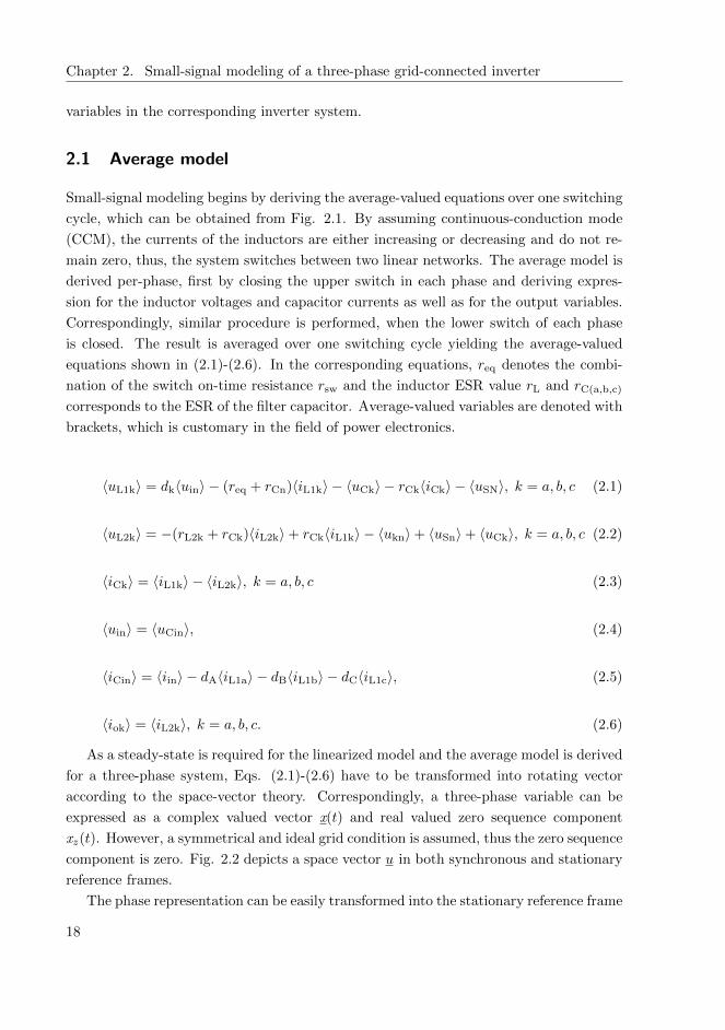
2.1 Average model
Small-signal modeling begins by deriving the average-valued equations over one switching
cycle, which can be obtained from Fig. 2.1. By assuming continuous-conduction mode
(CCM), the currents of the inductors are either increasing or decreasing and do not re-
main zero, thus, the system switches between two linear networks. The average model is
derived per-phase, first by closing the upper switch in each phase and deriving expres-
sion for the inductor voltages and capacitor currents as well as for the output variables.
Correspondingly, similar procedure is performed, when the lower switch of each phase
is closed. The result is averaged over one switching cycle yielding the average-valued
equations shown in (2.1)-(2.6). In the corresponding equations, req denotes the combi-
nation of the switch on-time resistance rsw and the inductor ESR value rL and rC(a,b,c)
corresponds to the ESR of the filter capacitor. Average-valued variables are denoted with
brackets, which is customary in the field of power electronics.
〈uL1k〉 = dk〈uin〉 − (req + rCn)〈iL1k〉 − 〈uCk〉 − rCk〈iCk〉 − 〈uSN〉, k = a, b, c (2.1)
〈uL2k〉 = −(rL2k + rCk)〈iL2k〉+ rCk〈iL1k〉 − 〈ukn〉+ 〈uSn〉+ 〈uCk〉, k = a, b, c (2.2)
〈iCk〉 = 〈iL1k〉 − 〈iL2k〉, k = a, b, c (2.3)
〈uin〉 = 〈uCin〉, (2.4)
〈iCin〉 = 〈iin〉 − dA〈iL1a〉 − dB〈iL1b〉 − dC〈iL1c〉, (2.5)
〈iok〉 = 〈iL2k〉, k = a, b, c. (2.6)
As a steady-state is required for the linearized model and the average model is derived
for a three-phase system, Eqs. (2.1)-(2.6) have to be transformed into rotating vector
according to the space-vector theory. Correspondingly, a three-phase variable can be
expressed as a complex valued vector x(t) and real valued zero sequence component
xz(t). However, a symmetrical and ideal grid condition is assumed, thus the zero sequence
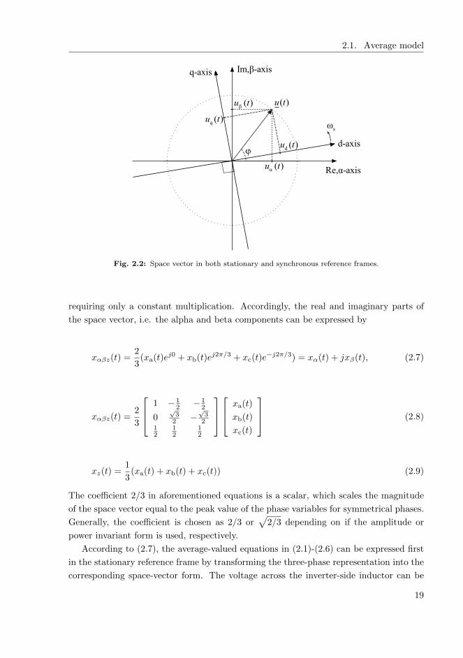
component is zero. Fig. 2.2 depicts a space vector u in both synchronous and stationary
reference frames.
The phase representation can be easily transformed into the stationary reference frame
18
2.1. Average model
Fig. 2.2: Space vector in both stationary and synchronous reference frames.
requiring only a constant multiplication. Accordingly, the real and imaginary parts of
the space vector, i.e. the alpha and beta components can be expressed by
xαβz(t) =2
3(xa(t)ej0 + xb(t)ej2π/3 + xc(t)e−j2π/3) = xα(t) + jxβ(t), (2.7)
xαβz(t) =2
3
1 − 12 − 1
2
0√
32 −
√3
212
12
12
xa(t)
xb(t)
xc(t)
(2.8)
xz(t) =1
3(xa(t) + xb(t) + xc(t)) (2.9)
The coefficient 2/3 in aforementioned equations is a scalar, which scales the magnitude
of the space vector equal to the peak value of the phase variables for symmetrical phases.
Generally, the coefficient is chosen as 2/3 or√
2/3 depending on if the amplitude or
power invariant form is used, respectively.
According to (2.7), the average-valued equations in (2.1)-(2.6) can be expressed first
in the stationary reference frame by transforming the three-phase representation into the
corresponding space-vector form. The voltage across the inverter-side inductor can be
19

Chapter 2. Small-signal modeling of a three-phase grid-connected inverter
given as (denoting vectors as underlined letters)
〈uL1〉 = −(req + rCa)〈iL1〉+ d〈uin〉 − 〈uCa〉+ rCa〈iL2〉
−2
3(ej0 + ej2π/3 + ej4π/3)〈uSN〉. (2.10)
The common-mode voltage uSN becomes zero as ej0 + ej2π/3 + ej4π/3 = 0, hence, Eq.
(2.10) can be presented by
〈uL1〉 = −(req + rC)〈iL1〉+ d〈uin〉 − 〈uC〉+ rC〈iL2〉. (2.11)
Furthermore, the grid-side inductor voltage can be given by
〈uL2 〉 = −(rL2 + rC)〈iL2〉+ rC〈iL1〉+ 〈uC〉 − 〈uo〉, (2.12)
and the filter capacitor current by
〈iC〉 = 〈iL1〉 − 〈iL2〉. (2.13)
As the stationary-reference-frame model cannot be linearized due to constantly vary-
ing operating point, the space-vector theory is applied to transform the aforementioned
equations into a synchronous reference frame by substituting xs(t) = x(t)e−jωst, where
the superscript ’s’ denotes the synchronous reference frame and ωs is the synchronous
frequency. According to the definition for the transformation, a grid angle is subtracted
from the rotating stationary reference frame counterpart and, thus, the vector in the
dq-domain appears to be constant. The synchronous reference frame representations for
(2.11)-(2.13) can be given according to transformation shown in (2.14).
〈iL1〉 = 〈isL1〉ejωst → d〈iL1〉dt
=d〈isL1〉
dtejωst + jωs〈isL1〉ejωst (2.14)
By substituting (2.14) into (2.11) and rearranging yields
d〈isL1〉dt
=1
L1
[ds〈uin〉 − (req + rC + jωsL1)〈isL1〉+ rC〈isL2〉 − 〈us
C〉]. (2.15)
Similar procedures are performed for all stationary-reference-frame variables and, accord-
20

2.1. Average model
ingly, the synchronous form for the grid-side inductor can be expressed by
d〈isL2〉dt
=1
L2
[− (rL2 + rC + jωsL2)〈isL2〉+ rC〈isL1〉+ 〈us
C〉 − 〈uso〉], (2.16)
and for capacitor voltage by
d〈usC〉
dt=
1
C
[〈isL1〉 − 〈isL2〉 − jωsCus
C〉]. (2.17)
The total current flowing into the inverter bridge, i.e., itot = iin− iCin, can be given with
the inverse Park’s transformation as itot = dA〈iL1a〉+dB〈iL1b〉+dC〈iL1c〉 = 32Reds〈isL1〉∗
= 32 [dd〈iL1d〉+ dq〈iL1q〉] and, therefore, the input-capacitor current can be expressed as
〈iCin〉 = 〈iin〉 −3
2
[dd〈iL1d〉+ dq〈iL1q〉
]. (2.18)
Consequently, the time derivative for the input capacitor voltage can be expressed by
d〈uCin〉dt
=1
Cin
[− 3
2(dd〈iL1d〉+ dq〈iL1q〉) + 〈iin〉
]. (2.19)
Furthermore, the input voltage and the output current can be expressed by
〈uin〉 = 〈uCin〉, (2.20)
〈iso〉 = 〈isL2〉. (2.21)
Considering the final steady-state formulation, Eqs. (2.15) - (2.21) in the synchronous
reference frame are divided into direct and quadrature components as xs(t) = xd(t) +
jxq(t). Note that Eq. (2.15) contains a uin-term which has to be replaced by (2.20). By
substituting (2.20) into (2.15) and dividing the average-valued equations into direct and
quadrature components yields:
d〈iL1d〉dt
=1
L1
[− (req + rC)〈iL1d〉+ ωsL1〈iL1q〉+ rC〈iL2d〉
−〈uCd〉+ dd〈uCin〉], (2.22)
21
Chapter 2. Small-signal modeling of a three-phase grid-connected inverter
d〈iL1q〉dt
=1
L1
[− (req + rC)〈iL1q〉 − ωsL1〈iL1d〉+ rC〈iL2q〉
−〈uCq〉+ dq〈uCin〉], (2.23)
d〈iL2d〉dt
=1
L2
[− (rL2 + rC)〈iL2d〉+ ωsL2〈iL2q〉+ rC〈iL1d〉+ 〈uCd〉 − 〈uod〉
], (2.24)
d〈iL2q〉dt
=1
L2
[− (rL2 + rC)〈iL2q〉 − ωsL2〈iL2d〉+ rC〈iL1q〉+ 〈uCq〉 − 〈uoq〉
], (2.25)
d〈uCin〉dt
=1
Cin
[− 3
2
(dd〈iL1d〉+ dq〈iL1q〉
)+ 〈iin〉
], (2.26)
d〈uCd〉dt
=1
C
[〈iL1d〉 − 〈iL2d〉+ ωsC〈uCq〉
], (2.27)
d〈uCq〉dt
=1
C
[〈iL1q〉 − 〈iL2q〉 − ωsC〈uCd〉
], (2.28)
〈uin〉 = 〈uCin〉, (2.29)
〈iod〉 = 〈iL2d〉, (2.30)
〈ioq〉 = 〈iL2q〉. (2.31)
Eqs. (2.22) - (2.31) are known as the synchronous-reference-frame average-valued model
for a current-fed VSI.
2.2 Operating point
The steady-state operating point can be obtained from the average-valued model by set-
ting the derivatives to zero and all the variables are replaced with their average-valued
terms denoted by corresponding upper case letters. As the inverter-side-inductor cur-
rent is the controlled variable, which is synchronized with the point-of-common coupling
(PCC) voltage, then IL1q = 0 and Uoq = 0 in the steady state. The q-component of
the inverter-side-inductor current (IL1q) is set to zero since unity power factor is desired.
However, a small amount of reactive power is transferred into the grid (i.e., IL2q 6= 0),
which is usually limited by proper selection of the capacitor.
By considering the operating conditions stated above, the steady state can be derived
22

2.2. Operating point
as
−ReqIL1d + rCIL2d − UCd +DdUin = 0, (2.32)
−k3IL1d + rCIL2q − UCq +DqUin = 0, (2.33)
Uin = UCin, (2.34)
−3
2DdIL1d + Iin = 0, (2.35)
−k1IL2q − UCd = 0, (2.36)
k1IL2d − k1IL1d − UCq = 0, (2.37)
k2UCq − k2RIL2q − IL2d = 0, (2.38)
Rk2IL2d − k2rCIL1d − k2UCd + k2Uod − IL2q = 0, (2.39)
where k1 = 1ωsC
, k2 = 1ωsL2
, Req = req + rC and R = rL2 + rC. Now by substituting
(2.36) and (2.37) into (2.38) and (2.39) and solving for IL2d and IL2q yield
IL2d =2IinKILd − 3DdRUod
3DdK(2.40)
and
IL2q = −2IinKILq + 3DdRUodKUo
3DdK, (2.41)
where KILd = k21 − k1k2 + RrC, KILq = k2rC + k1R − k1rC, KUo = k1 − k2 and K =
R2 + (k1 − k2)2. The steady-state for Dd and Dq can be calculated by substituting
(2.40) and (2.41) into (2.32) and (2.33), respectively. Appendix A provides a complete
MATLAB-code for calculating the steady state with parasitics. Simplified values for Dd
and Dq without the parasitic elements can be given by
Dd =Uod
Uin (1− CL2ω2s ), (2.42)
23

Chapter 2. Small-signal modeling of a three-phase grid-connected inverter
Dq =2
3
Iinωs
(L1 + L2 − L1L2Cω
2s
)Uod
. (2.43)
The linearization process is described in detail in the next section.
2.3 Linearized model
As can be seen from the average-valued model, some equations contain two input or
state variables multiplied with each other, e.g. d〈uCin〉. Therefore, the average model,
in this case, is actually nonlinear and does not suffice for a small-signal model due to
presence of nonlinear dependency between variables. Thus, the equations are linearized
by calculating partial derivatives for each state, input and output variables thus removing
the aforementioned nonlinearity. Accordingly, the obtained linearized equations can be
given by
diL1d
dt=
1
L1
[− (req + rC)iL1d + ωsL1iL1q + rCiL2d − uCd
+DduCin + Uindd
], (2.44)
diL1q
dt=
1
L1
[− (req + rC)iL1q − ωsL1iL1d + rCiL2q − uCq
+DquCin + Uindq
], (2.45)
diL2d
dt=
1
L2
[− (rL2 + rC)iL2d + ωsL2iL2q + rCiL1d + uCd − uod
], (2.46)
diL2q
dt=
1
L2
[− (rL2 + rC)iL2q − ωsL2iL2d + rCiL1q + uCq − uoq
], (2.47)
duCin
dt=
1
Cin
[− 3
2DdiL1d −
3
2DqiL1q + iin −
IinDd
dd
], (2.48)
duCd
dt=
1
C
[iL1d − iL2d + ωsCuCq
], (2.49)
duCq
dt=
1
C
[iL1q − iL2q − ωsCuCd
], (2.50)
24

2.3. Linearized model
uin = uCin, (2.51)
iod = iL2d, (2.52)
ioq = iL2q. (2.53)
According to (2.44) - (2.53), a linearized state-space can be formulated as
dx(t)
dt= Ax(t) + Bu(t)
y(t) = Cx(t) + Du(t)
(2.54)
where x = [iL1d, iL1q, iL2d, iL2q, uCd, uCq, uCin]T
represents a vector of state variables,
u = [iin, uod, uoq, dd, dq]T
represents a vector of input variables and y=[uin, iL1d, iL1q,
iod, ioq]T
is the vector for output variables. The state matrices in (2.54) can be given
according to (2.44)-(2.53) by
A =
− reqL1ωs
rCL1
0 − 1L1
0 Dd
L1
−ωs − reqL10 rC
L10 − 1
L1
Dq
L1
rCL2
0 − rL2+rCL2
ωs1L2
0 0
0 rCL2
−ωs − rL2+rCL2
0 1L2
01Cf
0 − 1Cf
0 0 ωs 0
0 1Cf
0 − 1Cf
−ωs 0 0
− 32Dd
Cin− 3
2Dq
Cin0 0 0 0 0
(2.55)
B =
0 0 0 Uin
L10
0 0 0 0 Uin
L1
0 − 1L2
0 0 0
0 0 − 1L2
0 0
0 0 0 0 0
0 0 0 0 01Cin
0 0 − IinDdCin
0
(2.56)
25
Chapter 2. Small-signal modeling of a three-phase grid-connected inverter
C =
0 0 0 0 1
1 0 0 0 0
0 1 0 0 0
0 0 1 0 0
0 0 0 1 0
(2.57)
D = 0 (2.58)
The linearized state-space can be given in the Laplace domain by replacing the derivative
operator ’d/dt’ with the Laplace-operator ’s’.
sX (s) = AX (s) + BU (s)
Y (s) = CX (s) + DU (s). (2.59)
In order to finalize the small-signal modeling procedure, the transfer functions between
input and output variables can be solved according to (2.59) as
Y (s) =[C(sI−A)−1B + D
]U (s) = GHU (s). (2.60)
The transfer function matrix GH is known as the H-parameter representation, i.e.,
when the inverter is analyzed as current-input-current-output system, which was dis-
cussed earlier considering the terminal constraints of the converter. Transfer functions
of the system can be given by
uin
iL1d
iL1q
iod
ioq
=
GH︷ ︸︸ ︷ZH
in THoi-d TH
oi-q GHci-d GH
ci-q
GHioL-d GH
oL-d GHoL-qd GH
cL-d GHcL-qd
GHioL-q GH
oL-dq GHoL-q GH
cL-dq GHcL-q
GHio-d −Y H
o-d −Y Ho-qd GH
co-d GHco-qd
GHio-q −Y H
o-dq −Y Ho-q GH
co-dq GHco-q
iin
uod
uoq
dd
dq
. (2.61)
Considering the second and third rows of the matrix, the subscript ’L’ denotes inverter-
side-current-related transfer functions, which are intermediate output variables. Note
that the topology of the converter dictates that the current should flow outwards into
26

2.3. Linearized model
the grid, but the output admittance is determined by the current flowing in it, which
is the opposite regarding the originally selected direction in Fig. 2.1. Therefore, the
output voltage uo-(d,q) actually perturbs a current opposite in sign and the corresponding
admittances Y Ho-d, Y H
o-qd, Y Ho-dq and Y H
o-q have to multiplied by a coefficient ’-1’.
In multi-variable systems, e.g., in the dq-domain analysis, the inputs, states and
outputs can have n channels. Correspondingly, variables can be given as one vector
consisting of two or more channels as x = [x1, x2, · · · , xn]T. Naturally for the dq-domain,
xs = [xd, xq]T, i.e., n = 2. Consequently, transfer functions between input and output
variable vectors can be modeled as n× n matrices, that is [76, 77]
G(s) =
G11 · · · G1n
.... . . G2n
Gn1 Gn2 Gnn
. (2.62)
The transfer matrix GH in (2.61) can be, thus, simplified and presented by using transfer
matrices due to the inherent multi-variable nature of the inverter [52, 76–79]. By com-
bining the d and q-components and their cross-coupling terms into two-by-two matrices,
the transfer function matrix GH in (2.61) can be given as
GH =
Zin Toi Gci
GioL GoL GcL
Gio −Yo Gco
. (2.63)
Note that according to topological properties of the inverter in Fig. 2.1, the input voltage
uin and the input current iin are scalar variables, hence, the input impedance Zin in (2.63)
is also a scalar.
Regarding the dynamical representation of the system, i.e. individual input-to-output
responses, corresponding transfer functions are presented for output variables with sep-
arate components as well as with the multi-variable representation in (2.64)-(2.71) ac-
cording to (2.61) and (2.63), respectively.
uin = ZHiniin + TH
oi-duod + THoi-quoq +GH
ci-ddd +GHci-qdq (2.64)
uin = Ziniin + Toiuo + Gcid (2.65)
27

Chapter 2. Small-signal modeling of a three-phase grid-connected inverter
iL1d = GHioL-diin +GH
oL-duod +GHoL-qduoq +GH
cL-ddd +GHcL-qddq (2.66)
iL1q = GHioL-qiin +GH
oL-dquod +GHoL-quoq +GH
cL-dqdd +GHcL-qdq (2.67)
iL1 = GioLiin + GoLuo + GcLd (2.68)
iod = GHio-diin − Y H
o-duod − Y Ho-qduoq +GH
co-ddd +GHco-qddq (2.69)
ioq = GHio-qiin − Y H
o-dquod − Y Ho-quoq +GH
co-dqdd +GHco-qdq (2.70)
iL2 = Gioiin −Youo + Gcod (2.71)
In the aforementioned open-loop output dynamics, considering (2.64) and (2.65), Zin
is the input impedance of the system, Toi-(d,q) is known as the reverse transfer function
and Gci-(d,q) is the control-to-input-voltage transfer function. Output current dynam-
ics can be presented by (2.66)-(2.68) for the inverter-side current and by (2.69)-(2.71)
for the grid current. Accordingly, Gio,ioL-(d,q) represent the input-to-output transfer
function or the forward current gain, Yo-(d,q,qd,dq) is the output admittance with cross-
coupling elements, GoL-(d,q,qd,dq) is the output-to-inductor current transfer function with
cross-coupling elements, Gco,cL-(d,q,qd,dq) is known as the control-to-output-current trans-
fer function, which also includes cross-coupling terms between components as shown in
(2.66)-(2.71).
A linear network model, which characterizes the terminal and dynamical behavior of
the converter, depicted in Fig. 2.3, can be presented according to the transfer function
matrix (2.63). The effect of the non-ideal source and load is included as a parallel in-
put admittance Ys and a series grid impedance Zg, respectively. Moreover, the CL-part
of the filter is shown separately for demonstrative purposes in order to highlight the
intermediate-output-variable-like nature of the inverter-side inductor current. Accord-
ingly, the aforementioned linear network model needs to be further elaborated as the
CL-part and corresponding transfer functions are not yet determined.
The small-signal model of the CL-filter can be derived according to Fig. 2.4, where
the filter input variables are the inverter-side inductor currents iL1(a,b,c) and the grid
phase-voltages uo(a,b,c)n. Furthermore, the filter output variables are the voltages across
the capacitors uC(a,b,c) and the output currents iL2(a,b,c). Accordingly, by applying well-
known averaging methods shown earlier, state matrices for the CL-filter can be given
by
28

2.3. Linearized model
Fig. 2.3: Source-load-affected open-loop model of a three-phase grid-connected PV inverter.
Af =
− rL2+rC
L2ωs
1L2
0
−ωs − rL2+rCL2
0 1L2
1C 0 0 0
0 1C 0 0
, (2.72)
Bf =
rCL2
0 1L2
0
0 rCL2
0 − 1L2
1 0 0 0
0 1 0 0
, (2.73)
Cf =
−rC 0 1 0
0 −rC 0 1
1 0 0 0
0 1 0 0
, (2.74)
Df =
rC 0 0 0
0 rC 0 0
0 0 0 0
0 0 0 0
. (2.75)
Clearly, switches are absent from the filter model and, therefore, only one linear circuit
is present. The obtained average-valued model is, in fact, also the linear representation
of the filter. Accordingly, the transfer function matrix of the filter can be given by
29

Chapter 2. Small-signal modeling of a three-phase grid-connected inverter
L1ai
L1bi
L1ci
C(a,b,c)u
L2(a,b,c)u
fau
fbu
fcu
oau
obu
ocu
Fig. 2.4: Linear model of a CL-type filter.
ufd
ufq
iL2d
iL2q
=
Zinf−d Zinf−qd Toif−d Toif−qd
Zinf−dq Zinf−q Toif−dq Toif−q
Giof−d Giof−qd −Yof−d −Yof−qd
Giof−dq Giof−q −Yof−dq −Yof−q
iL1d
iL1q
uod
uoq
(2.76)
Similarly, it should be noted that Eq. (2.76) can be also presented by using the multi-
variable notation by
[uf
iL2
]=
[Zinf Toif
Giof −Yof
][iL1
uo
](2.77)
Matrices in (2.77) are used to represent the open-loop dynamics of a CL-filter shown in
Fig. 2.3.
2.4 Source-affected model
Photovoltaic generator induces varying dynamical resistance (rpv) connected across the
input terminal of the converter. This has to be considered in the dynamical model in
order to analyze the converter dynamics correctly [4]. As shown in Fig. 2.3, a non-ideal
source with finite admittance Ys is assumed here, which can be included in the open-loop
dynamics of the system. Accordingly, the real input current (iin) of the converter is
affected by the non-ideal source current iinS as well as the parallel admittance Ys and
can be expressed as
30
2.4. Source-affected model
iin = iinS − Ysuin. (2.78)
Consequently, the input voltage dynamics can be presented by substituting (2.78) into
the nominal open-loop input voltage dynamics as
uin = Zin
(iinS − Ysuin
)+ Toiuo + Gcid,
uin =Zin
1+ZinYsiinS +
Toi
1+ZinYsuo +
Gci
1+ZinYsd.
(2.79)
The source-affected input current can be expressed as in (2.80), which is then substituted
into the open-loop dynamics of the inverter and grid currents.
iin =
(1− ZinYs
1 + ZinYs
)iinS −
YsToi
1 + ZinYsuo −
YsGci
1 + ZinYsd. (2.80)
Accordingly, the source-affected dynamics for input voltage, inductor current and grid
current can be given by
uin =Zin
1 + ZinYsiinS +
Toi
1 + ZinYsuo +
Gci
1 + ZinYsd, (2.81)
iL1 = GioL
(1− ZinYs
1 + ZinYs
)iinS +
(GoL −GioL
YsToi
1 + ZinYs
)uo
+
(GcL −GioL
YsGci
1 + ZinYs
)d, (2.82)
iL2 = Gio
(1− ZinYs
1 + ZinYs
)iinS −
(Yo + Gio
YsToi
1 + ZinYs
)uo
+
(Gco −Gio
YsGci
1 + ZinYs
)d. (2.83)
The source-affected transfer function matrix can be given according to (2.81)-(2.83) by
31

Chapter 2. Small-signal modeling of a three-phase grid-connected inverter
Zsin Ts
oi Gsci
GsioL Gs
oL GscL
Gsio Ys
o Gsco
=
Zin
1+ZinYs
Toi
1+ZinYs
Gci
1+ZinYs
GioL
(1− ZinYs
1+ZinYs
)GoL −GioL
YsToi
1+ZinYsGcL −GioL
YsGci
1+ZinYs
Gio
(1− ZinYs
1+ZinYs
)−Yo −Gio
YsToi
1+ZinYsGco −Gio
YsGci
1+ZinYs
. (2.84)
The impedance-based stability analysis, elaborated in Chapter 4, can be carried out
for the input interface by investigating the impedance ratio (i.e., the minor loop gain)
Zin/Zs, Zs = 1/Ys. However, this is not in the scope of this thesis and is not discussed
further.
2.5 Load-affected model
So far, an ideal load (i.e., the utility grid) has been assumed in the analysis, which
translates to a zero series impedance with the stiff voltage load. However, a real grid
contains a finite input impedance, which can significantly affect the behavior of the
interconnected inverter and, therefore, the effect of the load should be considered as a
part of the converter dynamic model [50]. The procedure shown here yields the load-
affected model, which can be utilized to analyze the effect of the grid on an arbitrary
system transfer function.
The non-ideal load is shown in Fig. 2.3 as a series impedance Zg with the real grid
voltage uoL. It is assumed that no parallel components in the load impedance are present
for simplicity. Interactions at the output terminal may occur as the output current of the
converter affects the voltage at the PCC (uo) via the grid impedance. Correspondingly,
the grid voltage uoL affects the output current via the output admittance Yo.
Regarding the derivation of the load-affected small-signal model, Fig. 2.5 is used
instead of Fig. 2.3 in order to express the load-affected transfer functions according to
their nominal open-loop counterparts shown in (2.63). The grid current can be expressed
according to Fig. 2.5 by
io = Gioiin −Youo + Gcod. (2.85)
32
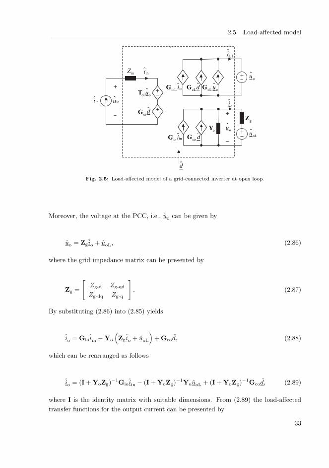
2.5. Load-affected model
Fig. 2.5: Load-affected model of a grid-connected inverter at open loop.
Moreover, the voltage at the PCC, i.e., uo can be given by
uo = Zgio + uoL, (2.86)
where the grid impedance matrix can be presented by
Zg =
[Zg-d Zg-qd
Zg-dq Zg-q
]. (2.87)
By substituting (2.86) into (2.85) yields
io = Gioiin −Yo
(Zgio + uoL
)+ Gcod, (2.88)
which can be rearranged as follows
io = (I + YoZg)−1Gioiin − (I + YoZg)−1YouoL + (I + YoZg)−1Gcod, (2.89)
where I is the identity matrix with suitable dimensions. From (2.89) the load-affected
transfer functions for the output current can be presented by
33

Chapter 2. Small-signal modeling of a three-phase grid-connected inverter
GLio = (I + YoZg)−1Gio, (2.90)
YLo = (I + YoZg)−1Yo, (2.91)
GLco = (I + YoZg)−1Gco, (2.92)
where the superscript ’L’ denotes the load-affected transfer functions.
The effect of the grid impedance on the inverter-side inductor current iL1 can be
derived as follows. By substituting (2.89) into (2.86) and solving for uo yields
uo = ZG[(I + YoZg)−1Gioiin − (I + YoZg)−1YouoL (2.93)
+(I + YoZg)−1Gcod] + uoL. (2.94)
Furthermore, the open-loop representation for inverter-side inductor current can be given
by
iL1 = GioLiin + GoLuo + GcLd. (2.95)
By substituting uo in (2.95) by (2.93) and solving for iL1 yields the load-affected inverter-
side inductor current, which can be now presented by
iL1 =[GioL + GoLZg(I + YoZg)−1Gio ]iin
+[GoL −GoLZg(I + YoZg)−1Yo]uoL
+[GcL + GoLZg(I + YoZg)−1Gco]d.
(2.96)
Accordingly, the load-affected transfer functions for the inverter-side inductor current
can be given by
GLioL = GioL + GoLZg(I + YoZg)−1Gio, (2.97)
GLoL = GoL −GoLZg(I + YoZg)−1Yo, (2.98)
GLcL = GcL + GoLZg(I + YoZg)−1Gco. (2.99)
34
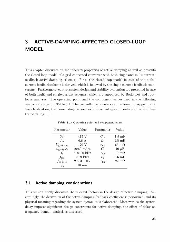
3 ACTIVE-DAMPING-AFFECTED CLOSED-LOOP
MODEL
This chapter discusses on the inherent properties of active damping as well as presents
the closed-loop model of a grid-connected converter with both single and multi-current-
feedback active-damping schemes. First, the closed-loop model in case of the multi-
current-feedback scheme is derived, which is followed by the single-current-feedback coun-
terpart. Furthermore, control system design and stability evaluation are presented in case
of both multi and single-current schemes, which are supported by Bode-plot and root-
locus analyses. The operating point and the component values used in the following
analysis are given in Table 3.1. The controller parameters can be found in Appendix B.
For clarification, the power stage as well as the control system configuration are illus-
trated in Fig. 3.1.
Table 3.1: Operating point and component values.
Parameter Value Parameter Value
Uin 415 V Cin 1.9 mFIin 6.6 A L1 2.5 mH
Ugrid,rms 120 V rL1 65 mΩωgrid, ωs 2π60 rad/s Cf 10 µF
fs 6–8–20 kHz rCf 10 mΩfres 2.29 kHz L2 0.6 mH
fs/fres 2.6–3.5–8.7 rL2 22 mΩrsw 10 mΩ
3.1 Active damping considerations
This section briefly discusses the relevant factors in the design of active damping. Ac-
cordingly, the derivation of the active-damping-feedback coefficient is performed, and its
physical meaning regarding the system dynamics is elaborated. Moreover, as the system
delay imposes significant design constraints for active damping, the effect of delay on
frequency-domain analysis is discussed.
35
Chapter 3. Active-damping-affected closed-loop model
Fig. 3.1: Depiction of the power stage and control system configuration.
3.1.1 Active damping feedback coefficient
The active damping affects the open-loop dynamics via the capacitor-current feedback
by changing the linearized equations describing the state-space of the converter (cf. Eqs.
(2.44)-(2.53)). This effect can be realized by replacing the perturbed duty ratio in the
open-loop state space by the active-damping-affected form. Accordingly, the selection
of the active damping gain as Rd/Uin can be well justified. By considering the effect
of active damping feedback on the system state space, its physical meaning can be also
clearly understood.
Active damping affects directly the perturbed duty ratio as (by neglecting the delay
for simplicity)
d = c−GADiCf, (3.1)
where c is the control-signal vector (i.e., the output of the current controller) and GAD
is the active damping transfer matrix. Different duty-ratio-affecting active damping
methods can be implemented by modifying the corresponding feedback matrix or the
feedback signal. However, only the capacitor-current-feedback method is discussed for
simplicity. Accordingly, the linearized state-space equations, directly affected by the duty
ratio perturbation, are the d and q-component of the inverter-side inductor current as
diL1d
dt=
1
L1
[− (req + rC) iL1d + ωsL1iL1q + rCiL2d
−uCfd +DduCin + Uindd
], (3.2)
36

3.1. Active damping considerations
diL1q
dt=
1
L1
[− (req + rC) iL1q − ωsL1iL1d + rCiL2q
−uCfq +DquCin + Uindq
], (3.3)
where req = rL1 + rswitch.
In a passively damped system, the filter capacitor is connected in series with an
additional damping resistor. Thus, considering Eqs. (3.2) and (3.3), the parameter rC
would be relatively high. Resonance damping is, therefore, achieved when the virtual
resistor Rd is implemented in series with the filter capacitor, i.e. rC,new = rC,old + Rd,
by modifying the duty ratios dd and dq. This is obtained when the d and q-component
duty ratios are modified as given in (3.4) and (3.5), respectively.
dd = cd −Rd
UiniCfd = cd −
Rd
Uin( iL1d − iL2d) (3.4)
dq = cq −Rd
UiniCfq = cq −
Rd
Uin( iL1q − iL2q) (3.5)
In Eqs. (3.4) and (3.5), Rd is the virtual resistor value and Uin is the steady-state input
voltage. The active damping gain matrix shown, e.g., in (3.25) can be formed according
to (3.4) and (3.5) yielding
GAD =
[Rd
Uin0
0 Rd
Uin
]. (3.6)
The effectiveness of the active damping can be adjusted by changing the value of the
virtual damping resistor Rd. It is worth noting that the use of virtual resistor incorporates
design constraints concerning the stability of the inverter. As discussed in [29, 80], the
effect of computation delay changes the behavior of the active damping feedback and
may introduce open-loop RHP poles into the control system. Accordingly, limitations
are imposed for the selection of the active damping gain. The effect of the delay can be
minimized by using modified feedback methods as discussed, e.g., in [33, 80–82]. The
active damping implementations, which mitigates the effect of the delay, are analyzed
further by means of the root locus analysis presented in Section 3.5.
37
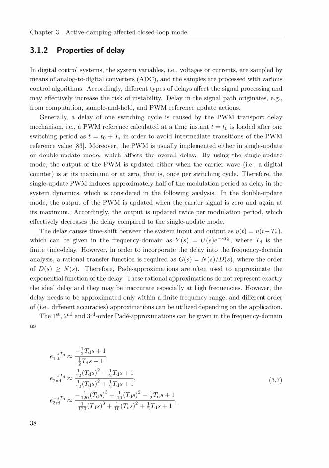
Chapter 3. Active-damping-affected closed-loop model
3.1.2 Properties of delay
In digital control systems, the system variables, i.e., voltages or currents, are sampled by
means of analog-to-digital converters (ADC), and the samples are processed with various
control algorithms. Accordingly, different types of delays affect the signal processing and
may effectively increase the risk of instability. Delay in the signal path originates, e.g.,
from computation, sample-and-hold, and PWM reference update actions.
Generally, a delay of one switching cycle is caused by the PWM transport delay
mechanism, i.e., a PWM reference calculated at a time instant t = t0 is loaded after one
switching period as t = t0 + Ts in order to avoid intermediate transitions of the PWM
reference value [83]. Moreover, the PWM is usually implemented either in single-update
or double-update mode, which affects the overall delay. By using the single-update
mode, the output of the PWM is updated either when the carrier wave (i.e., a digital
counter) is at its maximum or at zero, that is, once per switching cycle. Therefore, the
single-update PWM induces approximately half of the modulation period as delay in the
system dynamics, which is considered in the following analysis. In the double-update
mode, the output of the PWM is updated when the carrier signal is zero and again at
its maximum. Accordingly, the output is updated twice per modulation period, which
effectively decreases the delay compared to the single-update mode.
The delay causes time-shift between the system input and output as y(t) = u(t−Td),
which can be given in the frequency-domain as Y (s) = U(s)e−sTd , where Td is the
finite time-delay. However, in order to incorporate the delay into the frequency-domain
analysis, a rational transfer function is required as G(s) = N(s)/D(s), where the order
of D(s) ≥ N(s). Therefore, Pade-approximations are often used to approximate the
exponential function of the delay. These rational approximations do not represent exactly
the ideal delay and they may be inaccurate especially at high frequencies. However, the
delay needs to be approximated only within a finite frequency range, and different order
of (i.e., different accuracies) approximations can be utilized depending on the application.
The 1st, 2nd and 3rd-order Pade-approximations can be given in the frequency-domain
as
e−sTd1st ≈
− 12Tds+ 1
12Tds+ 1
,
e−sTd
2nd ≈112 (Tds)
2 − 12Tds+ 1
112 (Tds)
2+ 1
2Tds+ 1,
e−sTd
3rd ≈− 1
120 (Tds)3
+ 110 (Tds)
2 − 12Tds+ 1
1120 (Tds)
3+ 1
10 (Tds)2
+ 12Tds+ 1
.
(3.7)
38
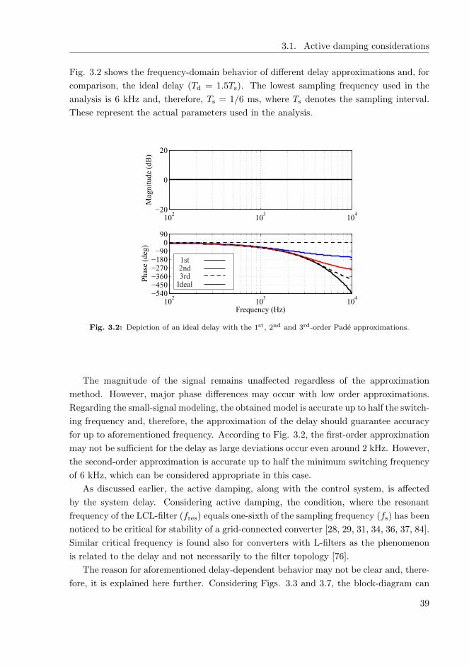
3.1. Active damping considerations
Fig. 3.2 shows the frequency-domain behavior of different delay approximations and, for
comparison, the ideal delay (Td = 1.5Ts). The lowest sampling frequency used in the
analysis is 6 kHz and, therefore, Ts = 1/6 ms, where Ts denotes the sampling interval.
These represent the actual parameters used in the analysis.
Fig. 3.2: Depiction of an ideal delay with the 1st, 2nd and 3rd-order Pade approximations.
The magnitude of the signal remains unaffected regardless of the approximation
method. However, major phase differences may occur with low order approximations.
Regarding the small-signal modeling, the obtained model is accurate up to half the switch-
ing frequency and, therefore, the approximation of the delay should guarantee accuracy
for up to aforementioned frequency. According to Fig. 3.2, the first-order approximation
may not be sufficient for the delay as large deviations occur even around 2 kHz. However,
the second-order approximation is accurate up to half the minimum switching frequency
of 6 kHz, which can be considered appropriate in this case.
As discussed earlier, the active damping, along with the control system, is affected
by the system delay. Considering active damping, the condition, where the resonant
frequency of the LCL-filter (fres) equals one-sixth of the sampling frequency (fs) has been
noticed to be critical for stability of a grid-connected converter [28, 29, 31, 34, 36, 37, 84].
Similar critical frequency is found also for converters with L-filters as the phenomenon
is related to the delay and not necessarily to the filter topology [76].
The reason for aforementioned delay-dependent behavior may not be clear and, there-
fore, it is explained here further. Considering Figs. 3.3 and 3.7, the block-diagram can
39
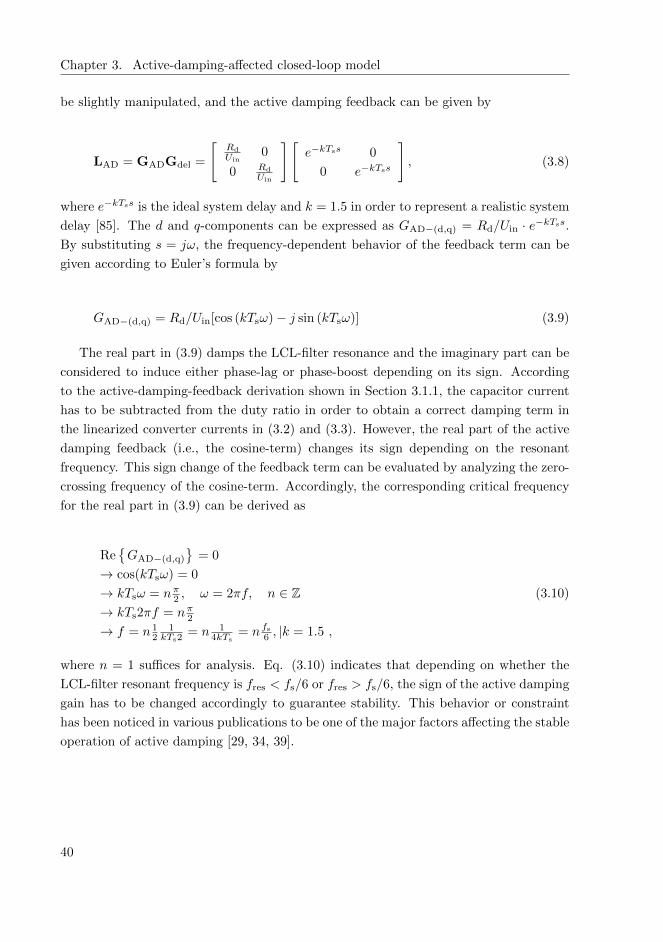
Chapter 3. Active-damping-affected closed-loop model
be slightly manipulated, and the active damping feedback can be given by
LAD = GADGdel =
[Rd
Uin0
0 Rd
Uin
][e−kTss 0
0 e−kTss
], (3.8)
where e−kTss is the ideal system delay and k = 1.5 in order to represent a realistic system
delay [85]. The d and q-components can be expressed as GAD−(d,q) = Rd/Uin · e−kTss.
By substituting s = jω, the frequency-dependent behavior of the feedback term can be
given according to Euler’s formula by
GAD−(d,q) = Rd/Uin[cos (kTsω)− j sin (kTsω)] (3.9)
The real part in (3.9) damps the LCL-filter resonance and the imaginary part can be
considered to induce either phase-lag or phase-boost depending on its sign. According
to the active-damping-feedback derivation shown in Section 3.1.1, the capacitor current
has to be subtracted from the duty ratio in order to obtain a correct damping term in
the linearized converter currents in (3.2) and (3.3). However, the real part of the active
damping feedback (i.e., the cosine-term) changes its sign depending on the resonant
frequency. This sign change of the feedback term can be evaluated by analyzing the zero-
crossing frequency of the cosine-term. Accordingly, the corresponding critical frequency
for the real part in (3.9) can be derived as
ReGAD−(d,q)
= 0
→ cos(kTsω) = 0
→ kTsω = nπ2 , ω = 2πf, n ∈ Z→ kTs2πf = nπ2→ f = n 1
21
kTs2= n 1
4kTs= n fs6 , |k = 1.5 ,
(3.10)
where n = 1 suffices for analysis. Eq. (3.10) indicates that depending on whether the
LCL-filter resonant frequency is fres < fs/6 or fres > fs/6, the sign of the active damping
gain has to be changed accordingly to guarantee stability. This behavior or constraint
has been noticed in various publications to be one of the major factors affecting the stable
operation of active damping [29, 34, 39].
40
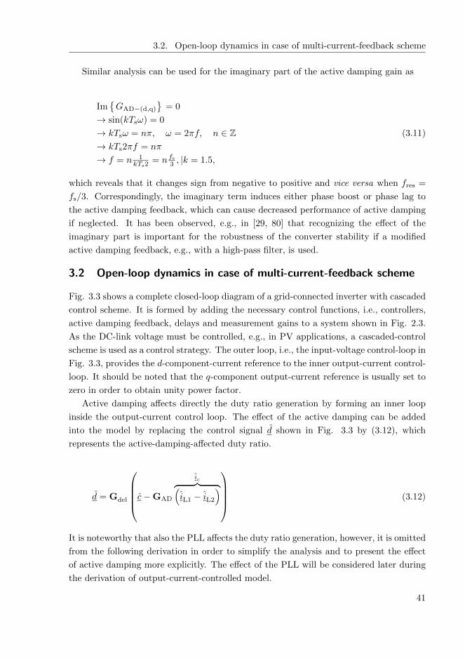
3.2. Open-loop dynamics in case of multi-current-feedback scheme
Similar analysis can be used for the imaginary part of the active damping gain as
ImGAD−(d,q)
= 0
→ sin(kTsω) = 0
→ kTsω = nπ, ω = 2πf, n ∈ Z→ kTs2πf = nπ
→ f = n 1kTs2
= n fs3 , |k = 1.5,
(3.11)
which reveals that it changes sign from negative to positive and vice versa when fres =
fs/3. Correspondingly, the imaginary term induces either phase boost or phase lag to
the active damping feedback, which can cause decreased performance of active damping
if neglected. It has been observed, e.g., in [29, 80] that recognizing the effect of the
imaginary part is important for the robustness of the converter stability if a modified
active damping feedback, e.g., with a high-pass filter, is used.
3.2 Open-loop dynamics in case of multi-current-feedback scheme
Fig. 3.3 shows a complete closed-loop diagram of a grid-connected inverter with cascaded
control scheme. It is formed by adding the necessary control functions, i.e., controllers,
active damping feedback, delays and measurement gains to a system shown in Fig. 2.3.
As the DC-link voltage must be controlled, e.g., in PV applications, a cascaded-control
scheme is used as a control strategy. The outer loop, i.e., the input-voltage control-loop in
Fig. 3.3, provides the d-component-current reference to the inner output-current control-
loop. It should be noted that the q-component output-current reference is usually set to
zero in order to obtain unity power factor.
Active damping affects directly the duty ratio generation by forming an inner loop
inside the output-current control loop. The effect of the active damping can be added
into the model by replacing the control signal d shown in Fig. 3.3 by (3.12), which
represents the active-damping-affected duty ratio.
d = Gdel
c−GAD
ic︷ ︸︸ ︷(iL1 − iL2
) (3.12)
It is noteworthy that also the PLL affects the duty ratio generation, however, it is omitted
from the following derivation in order to simplify the analysis and to present the effect
of active damping more explicitly. The effect of the PLL will be considered later during
the derivation of output-current-controlled model.
41

Chapter 3. Active-damping-affected closed-loop model
Fig. 3.3: Closed-loop control block diagram of a grid-connected converter with multi-current-feedback active damping.
According to the matrix given in (2.63), Eq. (3.12) can be expressed as a function of
input and control variables as in (3.13).
d = Gdelc−GdelGAD
(GioLiin + GoLuo + GcLd
−Gioiin −Youo −Gcod). (3.13)
Solving (3.13) for d yields
d = [I + GdelGAD (GcL −Gco)]−1
Gdel
[c−GADGioLiin (3.14)
−GADGoLuo + GADGioiin + GADYouo
].
By substituting (3.14) into the open-loop dynamics presented in Section 2.3, the active
damping-affected transfer functions can be solved. First, the input dynamics can be
given by
42

3.2. Open-loop dynamics in case of multi-current-feedback scheme
ZADin = Zin + Gci[I + GdelGAD (GcL −Gco)]
−1
×GdelGAD [Gio −GioL] , (3.15)
TADoi = Toi + Gci[I + GdelGAD (GcL −Gco)]
−1
×GdelGAD [Yo −GoL] , (3.16)
GADci = Gci[I + GdelGAD (GcL −Gco)]
−1Gdel, (3.17)
where ZADin , TAD
oi and GADci are the matrices for input impedance, transmittance and
control-to-input-voltage transfer functions, respectively.
Additionally, the input-current-to-inductor-current transfer function, output-voltage-
to-inductor-current transfer function and the control-to-inductor-current transfer func-
tions can be given as shown in (3.18)-(3.20), respectively.
GADioL = GioL + GcL[I + GdelGAD (GcL −Gco)]
−1
×GdelGAD [Gio −GioL] (3.18)
GADoL = GoL + GcL[I + GdelGAD (GcL −Gco)]
−1
×GdelGAD [Yo −GoL] (3.19)
GADcL = GcL[I + GdelGAD (GcL −Gco)]
−1Gdel (3.20)
Furthermore, the grid-current-related forward transfer function, output admittance and
control-to-grid-current transfer function can be given by
GADio = Gio + Gco[I + GdelGAD (GcL −Gco)]
−1
×GdelGAD [Gio −GioL] , (3.21)
YADo = Yo + Gco[I + GdelGAD (GcL −Gco)]
−1
×GdelGAD [Yo −GoL] , (3.22)
43

Chapter 3. Active-damping-affected closed-loop model
Fig. 3.4: Active damping control loop for the d and q-components (solid and dashed lines).
GADco = Gco[I + Gdel(GADGcL −GADGco)]
−1Gdel. (3.23)
The system delay matrix Gdel and active-damping-feedback-gain matrix GAD in Fig. 3.3
are as follows:
Gdel =
[1−k1s+k2s21+k1s+k2s2
0
0 1−k1s+k2s21+k1s+k2s2
](3.24)
GAD =
Rd
Uin0
0Rd
Uin
(3.25)
In Eq. (3.24), a second order Pade approximation is used to represent the ideal delay
(e−Tds) with k1 = 1/2 · Td and k2 = 1/12 · T 2d . The system delay is chosen as Td = 1.5Ts
according to [85], where Ts is the sampling interval. In practice, the delay consists of
PWM loading, analog-to-digital conversion and processing delays.
Considering the multi-current-feedback active damping implementation, the feedback
loop processes a signal from the capacitor current, which is a difference between the
inverter and grid currents (i.e., two output variables) as iC = iL1−iL2. Consequently, the
stability of the system may be affected, because the output variables are fed back into the
system. Conversely, if the processed variable would be an input variable, a feed-forward
loop is formed, which does not impose direct risk for instability. It is important to observe
44

3.3. Open-loop dynamics in case of single-current-feedback scheme
the fundamental nature of the active damping, which imposes a control-loop-like structure
as shown in Fig. 3.3 as well as in (3.15)-(3.23). The active-damping loop can be extracted
from aforementioned equations and presented as LAD = GdelayGAD(GcL −Gco).
In order to further elaborate the issue, active damping control loops for the d and q-
components are shown in Fig. 3.4, where the virtual resistor value Rd
= 15 Ω. Evidently,
the active-damping loop is effective only in vicinity of the resonant frequency, where the
loop regulates the capacitor current to its steady-state value. The open-loop system
transfer functions are, therefore, only affected around the corresponding frequency. This
is logical since the capacitor acts as an open circuit for lower frequencies, and the current
flows mainly through the two filtering inductors, L1 and L2. Accordingly, the low-
frequency active-damping-loop gain is negligible.
Other important transfer functions in the forthcoming analysis are the active-damping-
affected open-loop control-to-inverter-current and output admittance transfer functions
GADcL and YAD
o , respectively. Accordingly, the current control loop is designed with
GADcL , and the effect of active damping on the shape of the current control loop can be
analyzed. Furthermore, the effect of the operation point on the corresponding transfer
function should be addressed since it affects the control design.
The open-loop active-damping-affected output admittance can be used to examine the
active-damping-induced behavior around the resonant frequency, which is not affected by
the output-current control. Furthermore, the effect of the varying operating point at open
loop can be analyzed. The source-affected control-to-inductor-current transfer function
GADcL and output admittance YAD
o are presented in Figs. 3.5 and 3.6, respectively.
As can be observed, the shape of the transfer functions at higher frequencies remains
practically identical between different operating points, and the operating point affects
mainly the low-frequency behavior of the GADcL due to the operating-point-dependent
zero [4]. The low-frequency zero is located either in the RHP, imaginary axis or LHP
depending on the operating point (i.e., CCR, MPP or CVR), which causes input-voltage-
control-design constraints. These are discussed in detail in Section 3.4. Note that minor
gain differences between operating points at higher frequencies, especially in GADcL , are
also evident, which should be taken into account in the active damping design.
3.3 Open-loop dynamics in case of single-current-feedback scheme
In single-current-feedback scheme, the capacitor-current measurement is omitted, which
reduces the number of sensors required for operation. Instead, either the converter or grid
current is measured and the former is used in this thesis. Correspondingly, the measured
inverter-side current is used for both active damping and control purposes. Hence, the
duty ratio generation (cf. Fig. 3.7) is dependent only on one current instead of two,
which changes the active-damping-affected transfer functions shown in previous section.
45
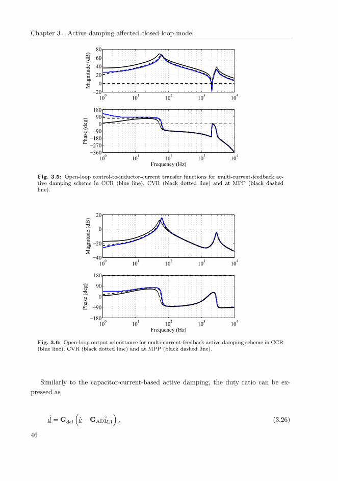
Chapter 3. Active-damping-affected closed-loop model
Fig. 3.5: Open-loop control-to-inductor-current transfer functions for multi-current-feedback ac-tive damping scheme in CCR (blue line), CVR (black dotted line) and at MPP (black dashedline).
Fig. 3.6: Open-loop output admittance for multi-current-feedback active damping scheme in CCR(blue line), CVR (black dotted line) and at MPP (black dashed line).
Similarly to the capacitor-current-based active damping, the duty ratio can be ex-
pressed as
d = Gdel
(c−GADiL1
), (3.26)
46

3.3. Open-loop dynamics in case of single-current-feedback scheme
Fig. 3.7: Closed-loop control block diagram of a grid-connected converter with single-current-feedback active damping.
which is substituted into the open-loop dynamics presented in (2.63). Thus, the active-
damping-affected duty ratio can be given by following the same procedure as in previous
section yielding
d = [I + GdelGADGcL]−1
Gdel
(c−GADGioLiin −GADGoLuo
). (3.27)
The transfer function representing the input dynamics can be given as follows.
ZADin = Zin + Gci[I + GdelGADGcL]
−1Gdel [−GADGioL] , (3.28)
TADoi = Toi + Gci [I + GdelGADGcL]
−1Gdel [−GADGoL] , (3.29)
GADci = Gci[I + GdelGADGcL]
−1Gdel, (3.30)
where ZADin , TAD
oi and GADci are the matrices for input impedance, transmittance and
control-to-input-voltage transfer functions, respectively.
Additionally, the input-current-to-inductor-current transfer function, output-voltage-
to-inductor-current transfer function and the control-to-inductor-current transfer func-
47

Chapter 3. Active-damping-affected closed-loop model
tions can be given as in (3.31)-(3.33), respectively.
GADioL = GioL + GcL[I + GdelGADGcL]
−1Gdel [−GADGioL] (3.31)
GADoL = GoL + GcL[I + GdelGADGcL]
−1Gdel [−GADGoL] (3.32)
GADcL = GcL[I + GdelGADGcL]
−1Gdel (3.33)
Furthermore, the output dynamics can be given by
GADio = Gio + Gco[I + GdelGADGcL]
−1Gdel [−GADGioL] , (3.34)
YADo = Yo + Gco[I + GdelGADGcL]
−1Gdel [−GADGoL] , (3.35)
GADco = Gco[I + GdelGADGcL]
−1Gdel. (3.36)
The system delay matrix Gdel and active damping feedback gain matrix GAD are as
given in Section 3.2 (cf. Eqs. 3.24 and 3.25).
According to the analogy presented to the multi-current-feedback active damping, a
feedback loop is formed by the single-current-feedback active damping as it feds back
the system output variable, which in this case is the inverter-side inductor current. The
active frequency ranges of the active damping loop are visible in Fig. 3.8 and its structure
in (3.28)-(3.36). The virtual resistor value was selected similarly to the multi-current-
feedback case as Rd
= 15 Ω. In case of the single-current-feedback scheme, the active-
damping loop gain can be given as LAD = GdelayGADGcL. Clearly, the loop gain lacks
the term Gco present in the multi-current-feedback counterpart, which naturally affects
the shape of the loop gain as shown in Fig. 3.8 for the d and q-components. It is
important to notice that the control gain is also active at the lower frequencies as well
as in vicinity of the filter resonant frequency. Consequently, the inverter-side inductor
acts as a short circuit at lower frequencies allowing the current to flow freely. This, in
turn, translates to substantial current signal in the active damping loop, and the active-
damping-affected transfer functions are modified for a wider frequency range than in case
of the multi-current-feedback scheme.
Similarly as in the previous section, active-damping-affected control-to-inverter-current
and output admittance transfer functions are shown here due to their importance in
the analysis later in this thesis. Figs. 3.9 and 3.10 show frequency responses of the
48

3.3. Open-loop dynamics in case of single-current-feedback scheme
Fig. 3.8: Active damping control loop for the d and q-components (solid and dashed lines).
Fig. 3.9: Open-loop control-to-output transfer functions for single-current-feedback active damp-ing scheme in CCR (blue line), CVR (black dotted line) and at MPP (black dashed line).
corresponding transfer functions, respectively. Comparing Figs. 3.9 and 3.10 to Figs.
3.5 and 3.6, it can be observed that the frequency responses are constant within the
active-damping loop gain. This behavior is caused by the direct control-loop-like struc-
ture of active damping, which induces a constant magnitude in the control-to-inductor-
current transfer function (iL1d/dd ≈ IL1d/Dd) within its bandwidth. Moreover, the
low-frequency behavior of GADcL exhibits similar phase shifting due to the operating-point-
dependent zero as was observed with multi-current-feedback scheme, although, its effect
49
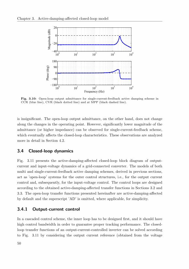
Chapter 3. Active-damping-affected closed-loop model
Fig. 3.10: Open-loop output admittance for single-current-feedback active damping scheme inCCR (blue line), CVR (black dotted line) and at MPP (black dashed line).
is insignificant. The open-loop output admittance, on the other hand, does not change
along the changes in the operating point. However, significantly lower magnitude of the
admittance (or higher impedance) can be observed for single-current-feedback scheme,
which eventually affects the closed-loop characteristics. These observations are analyzed
more in detail in Section 4.2.
3.4 Closed-loop dynamics
Fig. 3.11 presents the active-damping-affected closed-loop block diagram of output-
current and input-voltage dynamics of a grid-connected converter. The models of both
multi and single-current-feedback active damping schemes, derived in previous sections,
act as ’open-loop’ systems for the outer control structures, i.e., for the output current
control and, subsequently, for the input-voltage control. The control loops are designed
according to the obtained active-damping-affected transfer functions in Sections 3.2 and
3.3. The open-loop transfer functions presented hereinafter are active-damping-affected
by default and the superscript ’AD’ is omitted, where applicable, for simplicity.
3.4.1 Output-current control
In a cascaded control scheme, the inner loop has to be designed first, and it should have
high control bandwidth in order to guarantee proper tracking performance. The closed-
loop transfer functions of an output-current-controlled inverter can be solved according
to Fig. 3.11 by considering the output current reference (obtained from the voltage
50
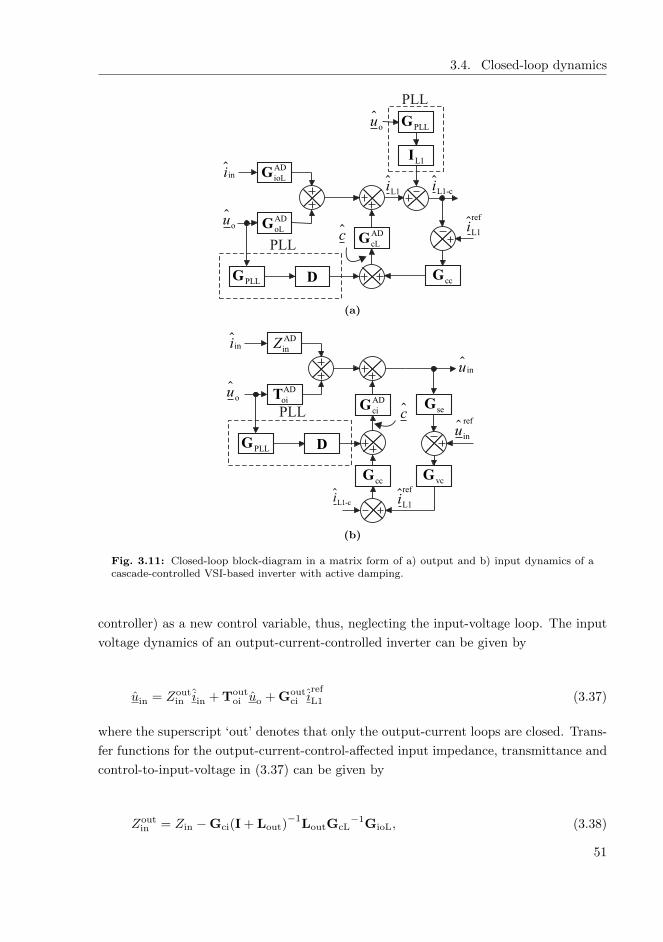
3.4. Closed-loop dynamics
(a)
(b)
Fig. 3.11: Closed-loop block-diagram in a matrix form of a) output and b) input dynamics of acascade-controlled VSI-based inverter with active damping.
controller) as a new control variable, thus, neglecting the input-voltage loop. The input
voltage dynamics of an output-current-controlled inverter can be given by
uin = Zoutin iin + Tout
oi uo + Goutci i
ref
L1 (3.37)
where the superscript ‘out’ denotes that only the output-current loops are closed. Trans-
fer functions for the output-current-control-affected input impedance, transmittance and
control-to-input-voltage in (3.37) can be given by
Zoutin = Zin −Gci(I + Lout)
−1LoutGcL
−1GioL, (3.38)
51
Chapter 3. Active-damping-affected closed-loop model
Toutoi = Toi −Gci(I + Lout)
−1 [LoutGcL
−1GoL
−LoutGcL−1IL1GPLL −DGPLL] , (3.39)
Goutci = Gci(I + Lout)
−1LoutGcL
−1, (3.40)
where the output-current loop gain Lout = GccGcL. Matrices D and IL1 are gains for
the steady-state duty-ratio and inductor current as shown in (3.41). The matrix GPLL
contains the PLL transfer functions, which can be expressed as follows [66].
D =
[0 Dq
0 Dd
], IL1 =
[0 IL1q
0 IL1d
](3.41)
GPLL =
[0 0
0 GPLL
], (3.42)
GPLL =1
Uod
LPLL
1 + LPLL, (3.43)
LPLL = −GPI−PLLUod
s, (3.44)
GPI−PLL = Kp +Ki
s. (3.45)
The matrices of the PI-based current controller Gcc can be given by
Gcc =
[Gcc−d 0
0 Gcc−q
]=
[Kp + Ki
s 0
0 Kp + Ki
s
](3.46)
Note that decoupling between the d and q-components in the current control is not uti-
lized and, therefore, the corresponding cross-coupling entries in (3.46) are null-elements.
Respectively, the inverter-side inductor current can be given by
52
3.4. Closed-loop dynamics
iL1 = GoutioL iin + Gout
oL uo + GoutcL u
refiL1 (3.47)
where the transfer function matrices are
GoutioL = GioL −GcL(I + Lout)
−1LoutGcL
−1GioL, (3.48)
GoutoL = GoL −GcL(I + Lout)
−1 [LoutGcL
−1GoL
−LoutGcL−1IL1GPLL −DGPLL] , (3.49)
GoutcL = GcL(I + Lout)
−1LoutGcL
−1. (3.50)
Furthermore, the grid-current dynamics can be given as follows.
GoutoL = GoL −Gco(I + Lout)
−1LoutGcL
−1GioL (3.51)
Youto = Yo −Gco(I + Lout)
−1 [LoutGcL
−1GoL
−LoutGcL−1IL1GPLL −DGPLL] (3.52)
Goutco = Gco(I + Lout)
−1LoutGcL
−1 (3.53)
The output-current control for both d and q-components is designed by shaping the
loop gain Lout. Accordingly, the bandwidth of the loop should be relatively high in order
to obtain good current tracking response and fast dynamics, which are required in grid-
connected applications in order to achieve good power quality. As shown earlier, the loop
is designed according to the active-damping-affected control-to-output transfer function
GcL, which is operating-point dependent [4]. Fig. 3.12 presents the loop gain in CCR,
CVR and at MPP in case of the multi-current-feedback active damping scheme.
As can be seen, the operating-point-dependent RHP-zero is induced at low frequencies
and the corresponding 180 degree phase transition from CCR to CVR and vice versa is
visible. If only the output-current control is used, the low-frequency RHP-zero limits
the current control bandwidth in the CCR, which would yield highly insufficient current
tracking performance. Therefore, the high-bandwidth current control is designed in the
CVR, which is stabilized by the cascaded control structure in the CCR. The operating-
point-dependent zero is, thus, considered only in the input-voltage-control design.
53

Chapter 3. Active-damping-affected closed-loop model
100
101
102
103
104
−60−40−20
0204060
Mag
nitu
de (
dB)
100
101
102
103
104
−360
−270
−180
−90
0
90
Pha
se (
deg)
Frequency (Hz)
Fig. 3.12: Output current loop gains for multi-current-feedback active damping scheme in CCR(blue line), CVR (black solid line) and at MPP (black dashed line).
100
101
102
103
104
−40
−20
0
20
40
60
Mag
nitu
de (
dB)
100
101
102
103
104
−360
−270
−180
−90
0
90
Pha
se (
deg)
Frequency (Hz)
Fig. 3.13: Output current loop gains for single-current-feedback active damping scheme in CCR(blue line), CVR (black solid line) and at MPP (black dashed line).
Regarding the single-current-feedback scheme, Fig. 3.13 shows the current-control
loop gain in case of the corresponding active damping scheme. As can be concluded from
the observations in Section 3.3, the resonant behavior near 100 Hz is absent. Moreover,
the inner active damping loop exhibits constant gain dynamics within its bandwidth
and, therefore, the shape of the output-current loop is determined by the current con-
troller. Accordingly, the characteristics of a pure I-controller (integral) are present since
the phase stays at -90 degrees with the gain decreasing by 20 dB/decade. Consequently,
54

3.4. Closed-loop dynamics
higher phase margin can be easily obtained within a wide frequency range, which sim-
plifies the control loop design and reduces risk for oscillation in the current response. In
addition, the operating-point-dependent behavior, visible in the multi-current-feedback
implementation, does not exist.
3.4.2 Input-voltage control
The input-voltage controller regulates the power extracted from the photovoltaic gener-
ator by adjusting the input voltage of the converter (or the output voltage of the PV
generator) according to the MPPT algorithms. This is performed indirectly by control-
ling the d-component of the output current and, therefore, the current flow into the input
capacitor. However, the role of the d-component in the controlling of the maximum power
might be unclear, which is explained next.
The instantaneous power of the DC-link capacitor can be given as PCin = dWCin/dt =
Cin/2·du2in/dt = Pin−Pout. As Pout = ReSout ≈ uodiod according to the instantaneous
power theory, the inverter-side inductor current iL1d (active-power-producing component)
indirectly controls the power flow into the input capacitor and, therefore, its reference
is determined by the input-voltage controller. Furthermore, since reactive power is not
controlled, the q-component of the inverter-side inductor current does not require an
outer control loop.
Fig. 3.14 shows the closed-loop block diagram of an input-voltage-controlled grid-
connected inverter. Similarly with the output-current-controlled converter in the previous
section, the input-voltage reference is considered as the new control variable. Further-
more, the input-voltage control loop generates the d-component of the inverter-side induc-
tor current reference (i.e., irefL1d). The output-current-control-affected transfer functions,
derived in the previous section, form the new ’open-loop’ system for the input-voltage
control.
The output-current reference can be presented according to Fig. 3.14b by
iref
L1 = GvcGseuin −Gvcurefin , (3.54)
where the vector for input-voltage reference, the voltage sensing gain matrix and voltage
controller matrix can be given by
urefin =
[uref
in
irefL1q
], (3.55)
55

Chapter 3. Active-damping-affected closed-loop model
(a)
(b)
Fig. 3.14: Closed-loop block-diagram in a matrix form of a) input and b) output dynamics of acascade-controlled VSI-based inverter with active damping.
Gse =
[Gse 0
0 0
]=
[1 0
0 0
], (3.56)
Gvc =
[−Gvc 0
0 1
]=
[− (Kp +Ki/s) 0
0 1
], (3.57)
respectively. Thus, the input voltage of the output-current-controlled inverter can be
expressed according to Fig. 3.14b by
uin = Zoutin iin + Tout
oi uo + Goutci i
ref
L1 . (3.58)
By substituting (3.54) into (3.58), the complete closed-loop input voltage dynamics can
be solved as
uin = (I + Lin)−1Zout
in iin + (I + Lin)−1
Toutoi uo − (I + Lin)
−1Gout
ci Gvcurefin , (3.59)
56

3.4. Closed-loop dynamics
where the input-voltage loop gain Lin = Goutci GvcGse. Hence, the closed-loop transfer
functions for input-voltage-controlled converter can be presented by
Ztotin = (I + Lin)
−1Zout
in , (3.60)
Ttotoi = (I + Lin)
−1Tout
oi , (3.61)
Gtotci = (I + Lin)
−1Gout
ci Gvc, (3.62)
where the superscript ’tot’ denotes the complete closed-loop transfer functions. Respec-
tively, the closed-loop dynamics for the inverter-side inductor current can be given as
iL1 = GtotioLiin + Gtot
oL uo + GtotcL u
refin , (3.63)
where
GtotioL = Gout
ioL −GoutcL GvcGse(I + Lin)
−1Zout
in , (3.64)
GtotoL = Gout
oL −GoutcL GvcGse(I + Lin)
−1Tout
oi , (3.65)
GtotcL = −Gout
cL
[GvcGse(I + Lin)
−1Gout
ci Gvc −Gvc
]. (3.66)
Similarly, the closed-loop transfer functions for the grid current are given as follows.
Gtotio = Gout
io −Goutco GvcGse(I + Lin)
−1Zout
in (3.67)
Ytoto = Yout
o −Goutco GvcGse(I + Lin)
−1Tout
oi (3.68)
Gtotco = −Gout
co
[GvcGse(I + Lin)
−1Gout
ci Gvc −Gvc
](3.69)
As discussed earlier, the d-component of the open-loop source-affected control-to-
inductor-current transfer function GcL−d incorporates an RHP-zero when the operating
point is in the CCR. This induces design constraints for the input-voltage control. Corre-
spondingly, analyzing the output-current-control-affected control-to-input transfer func-
57
Chapter 3. Active-damping-affected closed-loop model
tion Goutci−d, by neglecting the cross-couplings between the d and q-components, reveals
that
Goutci−d ≈
Gci−d
GcL−d
Lout−d
1 + Lout−d. (3.70)
The input-voltage control loop gain can be, therefore, given as
Lin = GseGvcGoutci−d ≈ GseGvcGci−d
1
GcL−d
Lout−d
1 + Lout−d
≈ GseGvcGci−d1
GcL−d, (3.71)
when Lout−d/(1 + Lout−d) ≈ 1 inside the output-current-control bandwidth. As can
be seen from (3.71), the control-to-inverter-current transfer function GcL−d is in the
denominator of the input-voltage loop gain Lin. Therefore, the RHP zero, which appears
in the CCR, turns to an RHP pole in the input-voltage control loop. This imposes design
constraints for the input-voltage controller and has to be taken into account in the control
design (i.e., minimum control bandwidth).
Usually, the maximum angular frequency of the pole is in the range of 1-20 Hz, and
can be expressed as [4, 6]
ωpole =Iin
CinUin. (3.72)
According to the control engineering principles, the control-loop bandwidth has to exceed
the RHP-pole frequency in order to guarantee stability. Another constraint for the input-
voltage-controller bandwidth comes from the input voltage ripple at 100 Hz caused by
unbalanced grid voltages. The bandwidth of the voltage controller should be designed to
provide enough attenuation at the aforementioned frequency in order to avoid polluting
the output-current reference (i.e., maximum control bandwidth).
The input-voltage-control-loop gains in case of both multi and single-current-feedback
active damping schemes are shown in Figs. 3.15 and 3.16, respectively. As is evident, the
effect of the active damping implementation is negligible on the voltage control dynamics
as it is active at higher frequencies. In the CVR, the photovoltaic generator resembles
an ideal voltage source, unaffected by the changing input current, thus the input voltage
control has very slow dynamics. Conversely, as the operating point shifts to the MPP and
CCR, the ideal current-source-like characteristics appear and higher control bandwidth
is obtained similarly for both operating points.
58
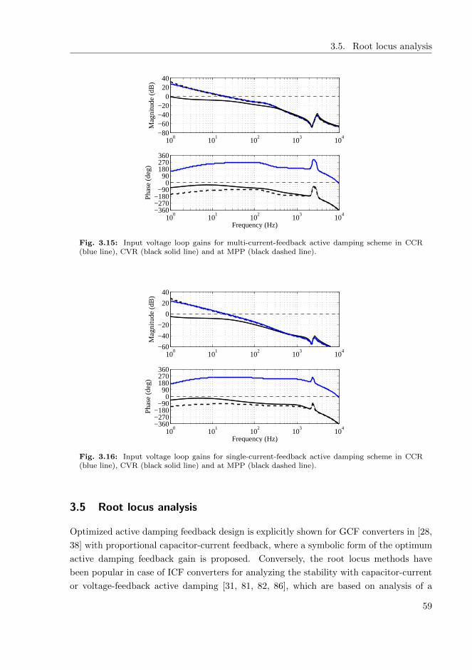
3.5. Root locus analysis
100
101
102
103
104
−80−60−40−20
02040
Mag
nitu
de (
dB)
100
101
102
103
104
−360−270−180−90
090
180270360
Pha
se (
deg)
Frequency (Hz)
Fig. 3.15: Input voltage loop gains for multi-current-feedback active damping scheme in CCR(blue line), CVR (black solid line) and at MPP (black dashed line).
100
101
102
103
104
−60
−40
−20
0
20
40
Mag
nitu
de (
dB)
100
101
102
103
104
−360−270−180−90
090
180270360
Pha
se (
deg)
Frequency (Hz)
Fig. 3.16: Input voltage loop gains for single-current-feedback active damping scheme in CCR(blue line), CVR (black solid line) and at MPP (black dashed line).
3.5 Root locus analysis
Optimized active damping feedback design is explicitly shown for GCF converters in [28,
38] with proportional capacitor-current feedback, where a symbolic form of the optimum
active damping feedback gain is proposed. Conversely, the root locus methods have
been popular in case of ICF converters for analyzing the stability with capacitor-current
or voltage-feedback active damping [31, 81, 82, 86], which are based on analysis of a
59

Chapter 3. Active-damping-affected closed-loop model
particular case and are not generally applicable. Optimum active damping feedback
for ICF converter is proposed in [32], which does not address the effect of the system
delay on the overall performance. Therefore, its validity regarding a real system with a
’worst-case’ delay is questionable.
Accordingly, this section presents the stability analysis regarding the active damping
design. Root-locus methods are often utilized, when determining the system stability
with varying operational parameter, which usually is the controller gain K. The same
methodology can be used also for active damping, where the system roots are drawn
with respect to the varying active-damping gain and, thus, stable ranges for the gain
can be obtained. The root-locus method could be replaced with Bode-plot analysis, but
the former can be considered more convenient in this case as the time-domain behavior
can be predicted. Additionally, root-locus methods are widely used in the literature
regarding the design of active damping [26, 33, 36, 80–82, 86]. The location of the system
roots determines the closed-loop transient response, i.e., the frequency and magnitude of
oscillations as well as the rate of exponential decay. The transient performance of the
current control also correlate with the output impedance characteristics, which is shown
later in Chapter 4.
The stability of the current control is analyzed by investigating the closed-loop transfer
function from the current reference to the output current, which was given in Section 3.4
as
GoutcL = GAD
cL (I + Lout)−1
Lout
(GAD
cL
)−1
. (3.73)
Analyzing Eq. (3.73) instead of only the active damping loop reveals the transient
behavior of the whole current loop. Practically, the performance of active damping
is, thus, simultaneously evaluated, which simplifies the stability analysis of the current
control. Note that only the d-component of (3.73) is analyzed in Sections 3.5.2 and 3.5.3,
because the resonant-frequency behavior between the d and q-components is similar.
3.5.1 Mitigation of delay in active damping feedback
The delay significantly changes the behavior of the active damping feedback, thus af-
fecting the converter stability. In order to improve the system stability characteristics,
high-pass-filtered (HPF) capacitor-current feedback method is proposed for GCF con-
verters in [80], where the HPF is used to mitigate the impact of the delay. Similar
filtered feedback implementations are also analyzed in Sections 3.5.2 and 3.5.3 in order
to improve the performance of active damping.
It was shown in Section 3.1.2 that also the imaginary part in (3.9) changes its sign
60

3.5. Root locus analysis
Fig. 3.17: Frequency-dependent behavior of the active damping feedback gain.
depending on the filter resonant frequency. This may not necessarily cause instability but
it can still worsen the performance of the converter. Generally, the frequency-dependent
behavior of active damping gain can be depicted as shown in Fig. 3.17. The real part is
positive when fres < fs/6 whereas the imaginary part is negative. Therefore, the effect of
the imaginary part is reduced by inducing phase boost on the feedback signal. However,
the real and imaginary parts have same signs when fs/6 < fres < fs/3. This does not
necessarily cause instability since the sign of the virtual resistor Rd can be changed.
However, the HPF cannot improve the system performance when fres > fs/6 since it
induces phase boost. To eliminate the effect of the imaginary part, a low-pass filter
(LPF) must be implemented in order to induce phase lag around the resonant frequency.
Correspondingly, by further increasing the resonant frequency to fs/3 < fres < fs/2,
where fs/2 is the Nyquist frequency, the real and imaginary parts have again the op-
posite signs. As a positive real part is required for active damping, the imaginary part
becomes negative after the feedback inversion. Therefore, active damping characteristics
are similar as in the case of fres < fs/6 and the HPF should be used to induce phase
boost in order to negate the effect of the imaginary part.
Considering the high and low-pass filters, the HPF can be presented in the s-domain
as GHPF = s/(s + ωcutoff) where ωcutoff is the desired cutoff frequency. The active
damping gain in (3.25) is multiplied by the corresponding transfer function, thus, the
virtual resistor value is used to adjust the gain of the HPF. Similarly, a low-pass filter
can be presented in the s-domain as GLPF = ωcutoff/(s + ωcutoff), where ωcutoff is the
desired cutoff frequency. Due to the lack of explicit design rules regarding the HPF or
LPF for ICF converters, the root locus diagrams in Sections 3.5.2 and 3.5.3 represent
only the most optimized cases for corresponding filtered feedback implementations.
61
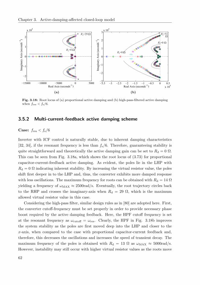
Chapter 3. Active-damping-affected closed-loop model
(a) (b)
Fig. 3.18: Root locus of (a) proportional active damping and (b) high-pass-filtered active dampingwhen fres < fs/6.
3.5.2 Multi-current-feedback active damping scheme
Case: fres < fs/6
Inverter with ICF control is naturally stable, due to inherent damping characteristics
[32, 34], if the resonant frequency is less than fs/6. Therefore, guaranteeing stability is
quite straightforward and theoretically the active damping gain can be set to Rd = 0 Ω.
This can be seen from Fig. 3.18a, which shows the root locus of (3.73) for proportional
capacitor-current-feedback active damping. As evident, the poles lie in the LHP with
Rd = 0 Ω indicating inherent stability. By increasing the virtual resistor value, the poles
shift first deeper in to the LHP and, thus, the converter exhibits more damped response
with less oscillations. The maximum frequency for roots can be obtained with Rd = 14 Ω
yielding a frequency of ωMAX ≈ 2500rad/s. Eventually, the root trajectory circles back
to the RHP and crosses the imaginary-axis when Rd = 29 Ω, which is the maximum
allowed virtual resistor value in this case.
Considering the high-pass filter, similar design rules as in [80] are adopted here. First,
the converter cutoff-frequency must be set properly in order to provide necessary phase
boost required by the active damping feedback. Here, the HPF cutoff frequency is set
at the resonant frequency as ωcutoff = ωres. Clearly, the HPF in Fig. 3.18b improves
the system stability as the poles are first moved deep into the LHP and closer to the
x-axis, when compared to the case with proportional capacitor-current feedback and,
therefore, this decreases the oscillations and increases the speed of transient decay. The
maximum frequency of the poles is obtained with Rd = 13 Ω as ωMAX ≈ 5000rad/s.
However, instability may still occur with higher virtual resistor values as the roots move
62

3.5. Root locus analysis
(a) (b)
Fig. 3.19: Root locus of (a) proportional active damping and (b) high-pass-filtered active dampingwhen fs/6 < fres < fs/3, ωHPF = ωres.
(a) (b)
Fig. 3.20: Root locus of (a) high-pass-filtered active damping and (b) low-pass-filtered activedamping when fs/6 < fres < fs/3, ωHPF = 0.2ωres, ωLPF = 2ωres.
back into the RHP at Rd = 51 Ω. Comparing Figs. 3.18a and 3.18b, it is evident that
the filtered feedback technique provides better current response (i.e., faster response with
less oscillations).
Case: fres > fs/6
Regarding the stability of the converter, decreasing the sampling frequency will sig-
nificantly affect the design of stable control system. When operating at frequencies
fres > fs/6, the converter is no longer inherently stable and active damping must be
used to ensure stable operation [34]. Similarly as for fres < fs/6, first the proportional
63

Chapter 3. Active-damping-affected closed-loop model
(a) (b)
Fig. 3.21: Root locus of (a) proportional active damping and (b) high-pass-filtered active dampingwhen fs/3 < fres < fs/2, ωHPF = 0.5ωres.
active damping feedback is analyzed when fs/6 < fres < fs/3 in Fig. 3.19a. Evidently,
using Rd = 0 Ω causes unstable inverter dynamics, since the poles are located in the
RHP, conversely to the case when fres < fs/6. However, similar parabolic root locus
can be seen comparing to the case with fres < fs/6 (cf. Figs. 3.18a and 3.18b). Ac-
cordingly, first the roots move deeper into the LHP, which indicates improved stability
margins. The maximum frequency of the roots is obtained when Rd = −12 Ω yielding
ωMAX ≈ 2200rad/s. Similarly, the roots move back into the RHP, when the virtual
resistor value is increased to Rd = −28 Ω.
As discussed earlier, the high-pass filter provides improved stability characteristics
when fres < fs/6. However, when fs/6 < fres < fs/3, the HPF will worsen the stability
characteristics, which is demonstrated in Fig. 3.19b, where the cutoff frequency was
chosen similarly as in the case for fres < fs/6, i.e., ω = ωres. Evidently, the HPF
causes the roots to stay in the RHP at least with the used parameters, which indicates
highly impaired stability margins. By lowering the HPF cutoff frequency from ω = ωres
to ω = 0.2ωres the stability can be recovered as shown in Fig. 3.20a. However, the
root trajectory is inferior compared to its proportional feedback counterpart shown in
Fig. 3.19a as the optimum root location is obtained with Rd = −6 Ω yielding ωMAX ≈200rad/s. Maximum virtual resistor value can be observed to be around Rd = −15 Ω.
To overcome the aforementioned stability problems, a low-pass filter must be imple-
mented to reduce the effect of the delay-imposed imaginary part of the active damping
feedback and to improve system stability. This case is shown in Fig. 3.20b, where the
LPF cutoff-frequency was chosen as ω = 2ωres. Clearly, the system poles move deeper
into the LHP compared to the case in Fig. 3.19a, which indicates fast and well-damped
64

3.5. Root locus analysis
step response of the current control. Accordingly, the most optimal properties regarding
the stability are obtained when Rd = −15 Ω yielding ωMAX ≈ 3500rad/s. Thus, the
converter exhibits improved current-control response compared to the proportional ac-
tive damping feedback and, therefore, the utilization of the low-pass filter is justified for
fs/6 < fres < fs/3.
The last distinct resonant frequency region is restricted only by the Nyquist frequency
as fs/3 < fres < fs/2, where the converter is still naturally unstable without the active
damping, since the roots are located in the RHP when Rd
= 0 Ω. However, the imaginary
part changes its sign from the previous case in this region and active damping feedback
dynamics resemble the case of fres < fs/6. Fig. 3.21a shows the root trajectory in case
of proportional active damping feedback when fs/3 < fres < fs/2. The optimal value
for the virtual resistor is Rd = −12 Ω yielding ωMAX ≈ 1500rad/s. Maximum value
is limited to Rd = −21 Ω. Moreover, the effect of the HPF is shown in Fig. 3.21b
with the HPF cutoff-frequency of ω = 0.5ωres. Clearly, the roots are moved deeper into
the LHP and the optimum current-controller response is obtained with Rd = −12 Ω,
ωMAX ≈ 2300rad/s, which is significantly better than with the proportional feedback
and, therefore, its necessity can be justified.
As a conclusion, it is important to acknowledge the overall effect of the delay on
the system stability. Accordingly, active damping design must be performed carefully,
especially with higher fres/fs-ratios. Furthermore, in order to eliminate the effect of
the system delay on the active damping performance, the selection of capacitor current
filtering method is essential. That is, a HPF should be utilized when fres < fs/6 and
fs/3 < fres < fs/2. Moreover, a LPF is necessary for improved robustness when fs/6 <
fres < fs/3.
3.5.3 Single-current-feedback active damping scheme
Design constraints on single-current-feedback scheme
As discussed earlier, the frequency region fres > fs/6 can be divided into two distinct
parts, similar to the multi-current feedback system, as the frequency-dependent behavior
of the delay does not change. Accordingly, fs/6 < fres < fs/3 and fs/3 < fres < fs/2
can be identified. However, the active damping loop changes the single-current-feedback
scheme profoundly, and the same design rules do not apply as for the multi-current
counterpart.
Regarding the available literature on the design constraints, it has been observed in
case of GCF converters that the system stability is difficult to achieve when fs/3 < fres <
fs/2 due to unavoidable nonminimum-phase characteristics [36]. In fact, fres < 0.28fs
has been found to be practical upper limit to the resonant frequency as the HPF imple-
mentation inside the control system becomes inaccurate due to the noise amplification
65

Chapter 3. Active-damping-affected closed-loop model
and sampling errors. This lowers the achievable operating range to fs/6 < fres < 0.28fs.
Similar restrictions can be found for ICF converter, which are analyzed through the
frequency-domain behavior of the active damping loop.
According to Figs. 3.3 and 3.7, the active damping loops for multi and single-current-
feedback schemes can be given by
LmultiAD−d = GdelayGAD(GcL−d −Gco−d)
LmultiAD−q = GdelayGAD(GcL−q −Gco−q)
, (3.74)
LsingleAD−d = GdelayGADGcL−d
LsingleAD−q = GdelayGADGcL−q
, (3.75)
respectively. Since the d and q-components in both open-loop GcL and Gco are practically
identical with each other at high frequencies, only the d-component is considered here
for simplicity. Fig. 3.22 shows the comparison of the active damping loop of multi and
single-current-feedback schemes. Additionally, for a single-current scheme, both negative
and positive damping gains (i.e., inverted and non-inverted) are presented. As discussed
in the previous section in case of multi-current-feedback scheme, the active damping
gain must be inverted to negative when the critical frequency (fres = fs/6) is exceeded.
However, in case of single-current-feedback scheme, this logic does not hold anymore.
The active damping loop under single-current-feedback system may pose instability
problems due to its phase behavior, and the instability is partially caused by the sign
of the active damping gain. Accordingly, it is evident from Fig. 3.22 that the phase
crosses over −180 degrees when |LsingleAD | ≥ 1 if a negative virtual resistor value is used.
This differs from the multi-current-feedback counterpart, where a negative value would
be used for active damping gain when fres > fs/6. Aforementioned phase crossing at
the middle frequencies can be overcome by using a positive active damping gain, but the
loop is still prone to instability due to the low phase margin in vicinity of the LCL-filter
resonant frequency.
In order to decrease the gain at the mid frequencies and increase the phase at the
higher frequencies, a high-pass filter is utilized. Ideally, a 90 degree phase boost could
be obtained with a pure derivative gain ‘s’. However, high-frequency noise would be
excessively amplified and, moreover, the realization of such ideal derivative element is
difficult. Instead, a high-pass filter, which can be implemented in digital controllers
quite easily, is used to produce the desired phase boost for a certain frequency range.
Accordingly, the filter cutoff frequency must be higher than the resonant frequency as
the phase boost is required for higher frequencies.
66

3.5. Root locus analysis
Fig. 3.22: Active damping loop gains for capacitor-current feedback with Rd ≤ 0 Ω (solid blackline), inverter-current feedback with Rd ≥ 0 Ω (blue dashed line) and inverter-current feedbackwith Rd ≤ 0 Ω (red dashed line). Note that the magnitude plots for inverter current feedbackactive damping overlap each other. Phase crossing over −180o is denoted with a vertical dashedline.
Fig. 3.23: Active damping loop gains for capacitor-current feedback (solid black line), inverter-current feedback with Rd ≥ 0 Ω (blue dashed line) and high-pass-filtered inverter-current feedbackwith Rd ≥ 0 Ω (black dash-dotted line).
Figs. 3.23 and 3.24 show the proportional and high-pass-filtered active damping
loop gains in case of single-current-feedback schemes as well as the proportional multi-
current-feedback counterpart. As evident in Fig. 3.24, if the HPF is not utilized, the
active damping loop exhibits two -180 degree crossings to the same direction (i.e., two
67

Chapter 3. Active-damping-affected closed-loop model
Fig. 3.24: Enlarged depiction of the resonant frequency behavior in Fig. 3.23. Phase crossingsover −180 degrees are denoted with red vertical dashed lines, fres > fs/6.
Fig. 3.25: Active damping loop gains for single-current-feedback schemes: HPF AD fs/6 < fres <fs/3 (solid blue line), HPF AD fs/3 < fres < fs/2 (solid red line) and proportional AD (dashedblack line). Note that the red line overlaps with the blue line in the upper figure.
Nyquist plot encirclements around (-1,0)) with |LsingleAD | ≥ 1 indicating unstable dynamics.
However, the high-pass filter increases the phase sufficiently and the stability can be,
therefore, guaranteed. Furthermore, the HPF prevents the low-frequency harmonics
from passing through the active damping loop and, therefore, the high-pass-filtered gain
exhibits highly attenuated low-frequency behavior and resembles the capacitor-current-
feedback active damping.
Considering the frequency region of fs/3 < fres < fs/2 in case of the single-current-
feedback scheme, stability is hardly achieved. Fig. 3.25 presents comparison between the
68

3.5. Root locus analysis
active damping loops when fs/3 < fres < fs/2 and fs/6 < fres < fs/3. Accordingly, the
sampling frequency is set exactly at fres = fs/3→ fs = 3fres. Clearly, the phase crosses
−180 degrees when |LsingleAD | ≥ 1 even with the phase boost induced by the HPF. Thus,
the observation agrees with the results proposed in [36] for GCF converters.
In conclusion, a high-pass filter must be used for single-current-feedback active damp-
ing when operating under fres > fs/6. Moreover, the limit for the minimum sampling
frequency can be given as fs ≈ 3fres, which is the same result as obtained for GCF
converters. Therefore, the same active damping design logic seems to apply for both
single-current-feedback ICF and GCF converters with active damping.
Case: fres < fs/6
Fig. 3.26a presents the root locus for proportional active damping in single-current-
feedback scheme. Regarding the resonant frequency region, active damping is not neces-
sarily required for stability, and the converter can operate with Rd = 0 Ω, which would
still lead to highly oscillatory as well as long transient response due to minimal stability
margins. By increasing the virtual resistor value, the stability margins can be improved
and the optimal damping is obtained when Rd = 23 Ω yielding ωMAX ≈ 2200rad/s.
The root locus crosses the imaginary-axis into the RHP when Rd = 41 Ω, which is the
maximum value for virtual resistor in this case.
(a) (b)
Fig. 3.26: Root locus of (a) proportional active damping and (b) high-pass-filtered active dampingwhen fres < fs/6, ωHPF = ωres.
As the frequency region of fres < fs/6 is considered, a high-pass filter should improve
the stability characteristics of active damping. Root locus for the corresponding case is
shown in Fig. 3.26b. Inherent stability is obtained similarly to the proportional feedback
case, but the root locus is inferior. More accurately, the roots do not move far from the
69
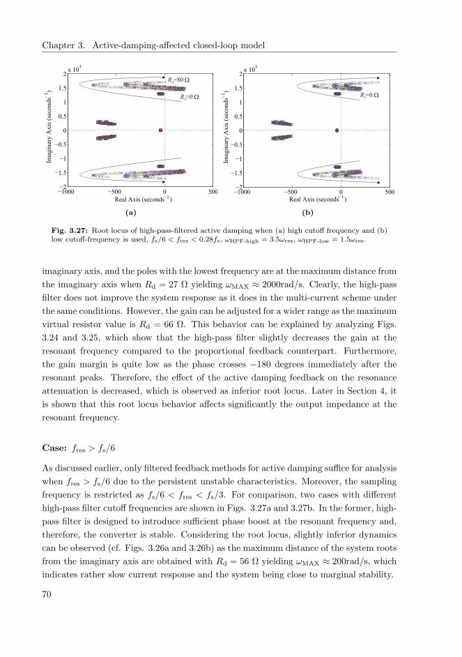
Chapter 3. Active-damping-affected closed-loop model
(a) (b)
Fig. 3.27: Root locus of high-pass-filtered active damping when (a) high cutoff frequency and (b)low cutoff-frequency is used, fs/6 < fres < 0.28fs, ωHPF-high = 3.5ωres, ωHPF-low = 1.5ωres.
imaginary axis, and the poles with the lowest frequency are at the maximum distance from
the imaginary axis when Rd = 27 Ω yielding ωMAX ≈ 2000rad/s. Clearly, the high-pass
filter does not improve the system response as it does in the multi-current scheme under
the same conditions. However, the gain can be adjusted for a wider range as the maximum
virtual resistor value is Rd = 66 Ω. This behavior can be explained by analyzing Figs.
3.24 and 3.25, which show that the high-pass filter slightly decreases the gain at the
resonant frequency compared to the proportional feedback counterpart. Furthermore,
the gain margin is quite low as the phase crosses −180 degrees immediately after the
resonant peaks. Therefore, the effect of the active damping feedback on the resonance
attenuation is decreased, which is observed as inferior root locus. Later in Section 4, it
is shown that this root locus behavior affects significantly the output impedance at the
resonant frequency.
Case: fres > fs/6
As discussed earlier, only filtered feedback methods for active damping suffice for analysis
when fres > fs/6 due to the persistent unstable characteristics. Moreover, the sampling
frequency is restricted as fs/6 < fres < fs/3. For comparison, two cases with different
high-pass filter cutoff frequencies are shown in Figs. 3.27a and 3.27b. In the former, high-
pass filter is designed to introduce sufficient phase boost at the resonant frequency and,
therefore, the converter is stable. Considering the root locus, slightly inferior dynamics
can be observed (cf. Figs. 3.26a and 3.26b) as the maximum distance of the system roots
from the imaginary axis are obtained with Rd = 56 Ω yielding ωMAX ≈ 200rad/s, which
indicates rather slow current response and the system being close to marginal stability.
70

3.5. Root locus analysis
As evident from Fig. 3.27b, the high-pass filter with low cutoff-frequency yields
unstable converter dynamics due to insufficient phase boost by the HPF, which was shown
in Fig. 3.24. It can be, therefore, concluded that single-current-feedback ICF converter
should be operated in the resonant frequency region of fres < fs/6 for improved stability.
Furthermore, the active damping design when operating under fres > fs/6 should be
performed carefully since the converter is highly susceptible to instability. Especially,
optimizing the HPF design and the active damping gain is essential.
71


4 OUTPUT IMPEDANCE WITH ACTIVE DAMPING
This chapter presents the output-impedance-properties of a three-phase grid-connected
inverter with active damping. The relation between the shape of the output impedance
and the active damping design is elaborated according to the observations regarding the
root-locus analysis in Sections 3.5.2 and 3.5.3. Furthermore, a comprehensive comparison
between the multi and single-current-feedback active damping schemes considering the
output impedance is presented.
4.1 Output impedance analysis
Regarding the output-impedance analysis, some practical matters are addressed next for
clarification. The output impedance (i.e., 1/Yo) is analyzed in this section as it is more
comprehensible regarding the impedance-based stability evaluation. However, the output
admittance is analyzed considering the active-damping-affected open-loop characteristics
in Section 4.2.
The effect of active damping on the output impedance is visible at frequencies higher
than the current-controller bandwidth due to lack of control gain in the current loop.
Accordingly, the most interesting properties of the impedance are concentrated in vicin-
ity of the resonant frequency and, therefore, the frequency-domain impedance plots are
presented only from 100 Hz upwards. It should be also noted that only the d-component
is analyzed, since the mid-to-high-frequency characteristics (>100 Hz) between the d and
q-components are nearly identical as shown later in Chapter 5.
4.1.1 Multi-current feedback scheme
Case: fres < fs/6
Fig. 4.1 shows the d-component of the output impedance with proportional capacitor-
current feedback. Accordingly, Rd values of [5, 15, 27] Ω are chosen for the analysis as
they represent the important points in the corresponding root locus in Fig. 3.18a, i.e.,
the minimum and maximum distances from the real and imaginary axes. Fig. 4.1 shows
that the shape of the impedance in vicinity of the resonant frequency varies as the virtual
resistor value is modified. First, by increasing the virtual resistor from Rd = 5 Ω (solid
line) to Rd = 15 Ω (dashed line) the magnitude of the impedance in vicinity of the
73
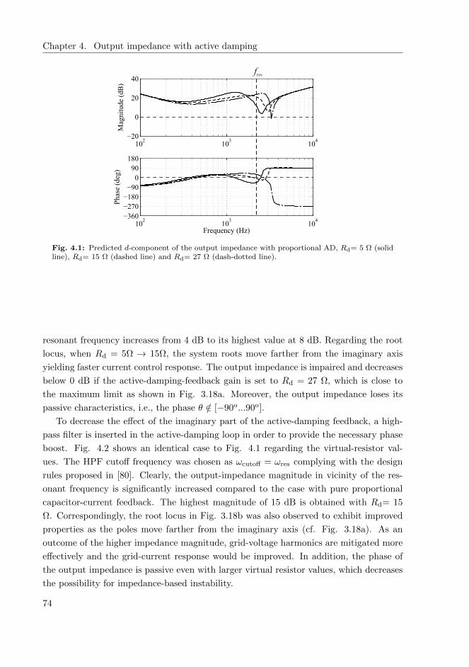
Chapter 4. Output impedance with active damping
Fig. 4.1: Predicted d-component of the output impedance with proportional AD, Rd= 5 Ω (solidline), Rd= 15 Ω (dashed line) and Rd= 27 Ω (dash-dotted line).
resonant frequency increases from 4 dB to its highest value at 8 dB. Regarding the root
locus, when Rd = 5Ω → 15Ω, the system roots move farther from the imaginary axis
yielding faster current control response. The output impedance is impaired and decreases
below 0 dB if the active-damping-feedback gain is set to Rd = 27 Ω, which is close to
the maximum limit as shown in Fig. 3.18a. Moreover, the output impedance loses its
passive characteristics, i.e., the phase θ /∈ [−90o...90o].
To decrease the effect of the imaginary part of the active-damping feedback, a high-
pass filter is inserted in the active-damping loop in order to provide the necessary phase
boost. Fig. 4.2 shows an identical case to Fig. 4.1 regarding the virtual-resistor val-
ues. The HPF cutoff frequency was chosen as ωcutoff = ωres complying with the design
rules proposed in [80]. Clearly, the output-impedance magnitude in vicinity of the res-
onant frequency is significantly increased compared to the case with pure proportional
capacitor-current feedback. The highest magnitude of 15 dB is obtained with Rd= 15
Ω. Correspondingly, the root locus in Fig. 3.18b was also observed to exhibit improved
properties as the poles move farther from the imaginary axis (cf. Fig. 3.18a). As an
outcome of the higher impedance magnitude, grid-voltage harmonics are mitigated more
effectively and the grid-current response would be improved. In addition, the phase of
the output impedance is passive even with larger virtual resistor values, which decreases
the possibility for impedance-based instability.
74
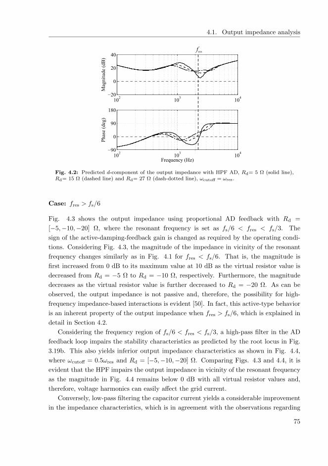
4.1. Output impedance analysis
Fig. 4.2: Predicted d-component of the output impedance with HPF AD, Rd= 5 Ω (solid line),Rd= 15 Ω (dashed line) and Rd= 27 Ω (dash-dotted line), ωcutoff = ωres.
Case: fres > fs/6
Fig. 4.3 shows the output impedance using proportional AD feedback with Rd =
[−5,−10,−20] Ω, where the resonant frequency is set as fs/6 < fres < fs/3. The
sign of the active-damping-feedback gain is changed as required by the operating condi-
tions. Considering Fig. 4.3, the magnitude of the impedance in vicinity of the resonant
frequency changes similarly as in Fig. 4.1 for fres < fs/6. That is, the magnitude is
first increased from 0 dB to its maximum value at 10 dB as the virtual resistor value is
decreased from Rd = −5 Ω to Rd = −10 Ω, respectively. Furthermore, the magnitude
decreases as the virtual resistor value is further decreased to Rd = −20 Ω. As can be
observed, the output impedance is not passive and, therefore, the possibility for high-
frequency impedance-based interactions is evident [50]. In fact, this active-type behavior
is an inherent property of the output impedance when fres > fs/6, which is explained in
detail in Section 4.2.
Considering the frequency region of fs/6 < fres < fs/3, a high-pass filter in the AD
feedback loop impairs the stability characteristics as predicted by the root locus in Fig.
3.19b. This also yields inferior output impedance characteristics as shown in Fig. 4.4,
where ωcutoff = 0.5ωres and Rd = [−5,−10,−20] Ω. Comparing Figs. 4.3 and 4.4, it is
evident that the HPF impairs the output impedance in vicinity of the resonant frequency
as the magnitude in Fig. 4.4 remains below 0 dB with all virtual resistor values and,
therefore, voltage harmonics can easily affect the grid current.
Conversely, low-pass filtering the capacitor current yields a considerable improvement
in the impedance characteristics, which is in agreement with the observations regarding
75
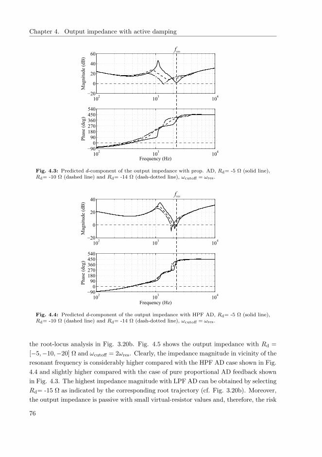
Chapter 4. Output impedance with active damping
Fig. 4.3: Predicted d-component of the output impedance with prop. AD, Rd= -5 Ω (solid line),Rd= -10 Ω (dashed line) and Rd= -14 Ω (dash-dotted line), ωcutoff = ωres.
Fig. 4.4: Predicted d-component of the output impedance with HPF AD, Rd= -5 Ω (solid line),Rd= -10 Ω (dashed line) and Rd= -14 Ω (dash-dotted line), ωcutoff = ωres.
the root-locus analysis in Fig. 3.20b. Fig. 4.5 shows the output impedance with Rd =
[−5,−10,−20] Ω and ωcutoff = 2ωres. Clearly, the impedance magnitude in vicinity of the
resonant frequency is considerably higher compared with the HPF AD case shown in Fig.
4.4 and slightly higher compared with the case of pure proportional AD feedback shown
in Fig. 4.3. The highest impedance magnitude with LPF AD can be obtained by selecting
Rd= -15 Ω as indicated by the corresponding root trajectory (cf. Fig. 3.20b). Moreover,
the output impedance is passive with small virtual-resistor values and, therefore, the risk
76

4.1. Output impedance analysis
Fig. 4.5: Predicted d-component of the output impedance with LPF AD, Rd= -5 Ω (solid line),Rd= -10 Ω (dashed line) and Rd= -20 Ω (dash-dotted line), ωcutoff = ωres.
Fig. 4.6: Predicted d-component of the output impedance with prop. AD, Rd= -5 Ω (solid line),Rd= -15 Ω (dashed line) and Rd= -25 Ω (dash-dotted line).
for impedance-based instability is negligible in that case. However, small virtual-resistor
value causes relatively low impedance magnitude in vicinity of the resonant frequency,
which indicates poor robustness against the grid-voltage harmonics.
By further changing the sampling frequency as fs/3 < fres < fs/2, the active damping
implementation must be again changed in order to achieve improved performance. Fig.
4.6 shows the output impedance with pure proportional active-damping feedback, where
Rd = [−5,−15,−25] Ω. The overall magnitude is low, which can be slightly improved
77
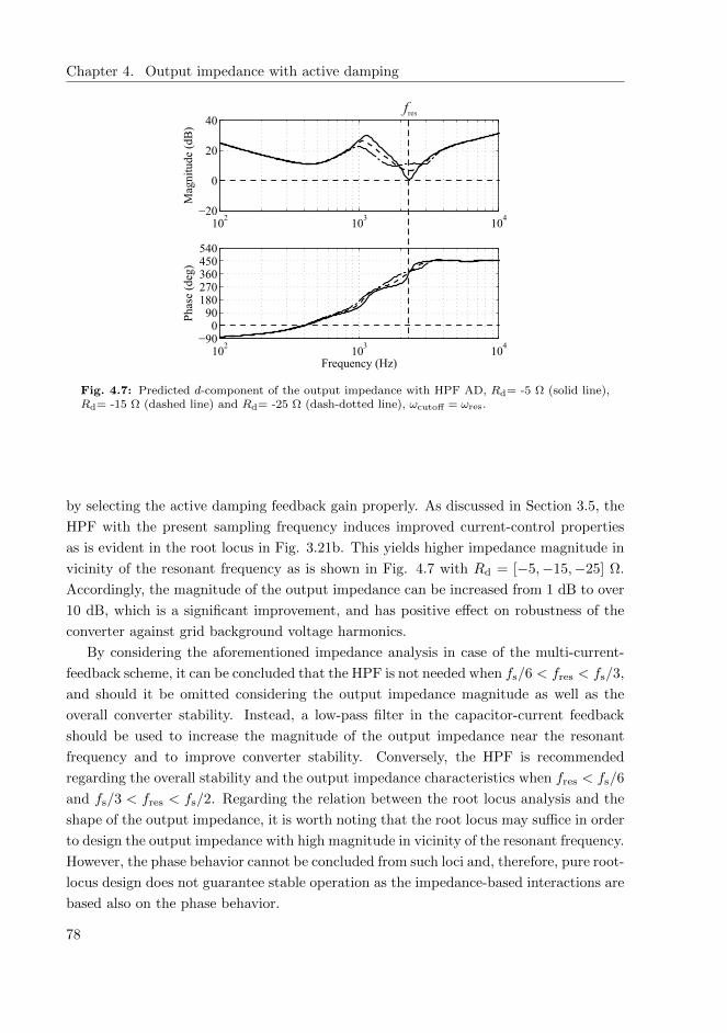
Chapter 4. Output impedance with active damping
Fig. 4.7: Predicted d-component of the output impedance with HPF AD, Rd= -5 Ω (solid line),Rd= -15 Ω (dashed line) and Rd= -25 Ω (dash-dotted line), ωcutoff = ωres.
by selecting the active damping feedback gain properly. As discussed in Section 3.5, the
HPF with the present sampling frequency induces improved current-control properties
as is evident in the root locus in Fig. 3.21b. This yields higher impedance magnitude in
vicinity of the resonant frequency as is shown in Fig. 4.7 with Rd = [−5,−15,−25] Ω.
Accordingly, the magnitude of the output impedance can be increased from 1 dB to over
10 dB, which is a significant improvement, and has positive effect on robustness of the
converter against grid background voltage harmonics.
By considering the aforementioned impedance analysis in case of the multi-current-
feedback scheme, it can be concluded that the HPF is not needed when fs/6 < fres < fs/3,
and should it be omitted considering the output impedance magnitude as well as the
overall converter stability. Instead, a low-pass filter in the capacitor-current feedback
should be used to increase the magnitude of the output impedance near the resonant
frequency and to improve converter stability. Conversely, the HPF is recommended
regarding the overall stability and the output impedance characteristics when fres < fs/6
and fs/3 < fres < fs/2. Regarding the relation between the root locus analysis and the
shape of the output impedance, it is worth noting that the root locus may suffice in order
to design the output impedance with high magnitude in vicinity of the resonant frequency.
However, the phase behavior cannot be concluded from such loci and, therefore, pure root-
locus design does not guarantee stable operation as the impedance-based interactions are
based also on the phase behavior.
78

4.1. Output impedance analysis
4.1.2 Single-current-feedback scheme
As discussed in Section 3.5.3, the single-current-feedback scheme exhibits inherent con-
straints for the control system design, which, in turn, limits the analysis of the output
impedance for resonant frequency regions of fres < fs/6 and fs/6 < fres < fs/3. In the
naturally stable frequency region, both proportional and HPF active damping feedback
schemes are analyzed. Conversely, for fres > fs/6, only the HPF feedback scheme is
evaluated.
Case: fres < fs/6
Fig. 4.8 shows the output impedance with proportional active damping feedback using
virtual resistor values of Rd = [−10,−20,−30] Ω. As can be observed, the behavior
of the impedance magnitude is similar to the multi-current-feedback scheme due to the
parabolic root locus (cf. Fig. 3.26a), which induces corresponding behavior on the
output impedance. Accordingly, the magnitude is at highest, when the root trajectory is
farthest from the imaginary axis as shown in Fig. 3.26a with Rd = −21 Ω. However, the
magnitude from 100 Hz to 1 kHz is increased compared to its multi-current-feedback-
scheme counterpart shown in Fig. 4.1. The impedance exhibits also a phase flip over 180
degrees at lower frequencies, when a small active damping gain is used, which indicates
a positive real part and non-passivity of the impedance, i.e., ReZo ≥ 0.
Regarding the magnitude increase when 100 < f < 1000 Hz, it is related to the
active-damping-affected open-loop dynamics, which are more elaborated in Section 4.2.
The low-frequency phase flip, in turn, was observed to be related to the design of the
input-voltage control. More precisely, the input-voltage-control loop should contain a
high phase margin in order to avoid the low-frequency phase flip. However, the input-
control optimization regarding the aforementioned phenomenon is not included in this
thesis, although it affects the impedance-based behavior of the converter and should be
addressed in the future research. A simple method to overcome the active-type impedance
in this case is by the filtering the active-damping feedback, which maintains the passive
output-impedance characteristics.
Fig. 4.9 shows the output impedance affected by the HPF active-damping method
with Rd = [−10,−20,−30] Ω and ωcutoff = ωres. It can be observed that the phase of
the impedance is passive, and the low-frequency phase flip shown in Fig. 4.8 is absent.
However, the output impedance magnitude in vicinity of the resonant frequency can be
considered slightly inferior or equivalent compared to the case with pure proportional
active-damping feedback, which is in accordance with the root-locus analysis shown in
Figs. 3.26a and 3.26b. Furthermore, the magnitude increase in the range of 100-1000 Hz
observed in the pure proportional active-damping scheme is absent, because the charac-
79

Chapter 4. Output impedance with active damping
Fig. 4.8: Predicted d-component of the output impedance with proportional AD, Rd= -10 Ω (solidline), Rd= -20 Ω (dashed line) and Rd= -30 Ω (dash-dotted line).
Fig. 4.9: Predicted d-component of the output impedance with HPF AD, Rd= -10 Ω (solid line),Rd= -20 Ω (dashed line) and Rd= -30 Ω (dash-dotted line), ωcutoff = ωres.
teristics resemble the capacitor-current-feedback active damping as discussed in Section
3.5.3.
Case: fres > fs/6
Only the filtered active-damping-feedback implementation provides stable dynamics,
when fres > fs/6 in case of the single-current-feedback scheme. Accordingly, Fig. 4.10
80

4.2. Comparison of single and multi-current-feedback schemes
Fig. 4.10: Predicted d-component of the output impedance with HPF AD, Rd= 20 Ω (solid line),Rd= 40 Ω (dashed line) and Rd= 60 Ω (dash-dotted line), ωcutoff = 3.5ωres.
shows the output impedance with incrementing virtual resistor value as Rd = [20, 40, 60]
Ω. The high-pass-filter cutoff frequency was set at relatively high frequency (ωcutoff =
3.5ωres) in order to provide the necessary phase boost at the resonant frequency. Evi-
dently, the shape of the impedance resembles the case shown in Fig. 4.9 for fres < fs/6.
Regarding the root locus shown in Fig. 3.27a, it is hard to obtain high output impedance
in this case as the roots stay in the vicinity of the imaginary axis. The highest magnitude
is obtained by setting the virtual resistor value between 50-60, which subsequently yields
an impedance magnitude of around 5 dB. Moreover, the output impedance is passive,
which is contrary to the multi-current-feedback scheme operating under fres > fs/6. The
explanation for the aforementioned behavior is given in the following section.
4.2 Comparison of single and multi-current-feedback schemes
Considering the analysis in the previous sections, the multi and single-current-feedback
active-damping schemes exhibit different output admittance properties, yet the causes
might not be clear. For example, the single-current-feedback scheme has lower admit-
tance below the resonant frequency. When the HPF is utilized, it resembles the behavior
of the multi-current-feedback active damping scheme. Moreover, the admittance remains
passive in case of the single-current-feedback implementation when fres > fs/6. Ac-
cordingly, this section discusses the matter by analyzing the detailed effect of the active
damping on specific system transfer functions in order to clarify the observed properties
such as:
81

Chapter 4. Output impedance with active damping
• The differences in the low-frequency (100-1000 Hz) magnitude of the output ad-
mittance between the single and multi-current-feedback schemes.
• The non-passivity of the output admittance in case of the multi-current-feedback
active damping implementation inside the frequency region of 500 < f < 2000 Hz.
4.2.1 Magnitude of output admittance
The active-damping feedback modifies the corresponding open-loop transfer functions
inside its control bandwidth as discussed in Sections 3.2 and 3.3. Therefore, in the multi-
current-feedback scheme, the transfer functions are modified in vicinity of the resonant
frequency, and the single-current-feedback scheme modifies the transfer functions also
at medium frequencies. Accordingly, Eqs. (4.1) and (4.2) present the active-damping-
affected output admittances (cf. Eqs. 3.22 and 3.35) as
Y AD−multio−d = Yo−d −
GdelayGADGco−d (GoL−d − Yo−d)
1 +GdelayGAD (GcL−d −Gco−d)
= Yo−d −Lmulti
AD−d
1 + LmultiAD−d
Gco−d (GoL−d − Yo−d)
GcL−d −Gco−d
= Yo−d −Gmultimod−d,
(4.1)
for the multi-current scheme, and
Y AD−singleo−d = Yo−d −
GdelayGADGco−dGoL−d
1 +GdelayGADGcL−d
= Yo−d −Lsingle
AD−d
1 + LsingleAD−d
Gco−dGoL−d
GcL−d
= Yo−d −Gsinglemod−d,
(4.2)
for the single-current-feedback scheme. Note that Lmulti/singleAD−d /(1 + L
multi/singleAD−d ) ≈ 1
within the active-damping-loop bandwidth, where the active-damping-affected multi and
single-current-feedback scheme output admittances are changed by the corresponding
modifier terms, i.e., Gco−d (GoL−d − Yo−d)/(GcL−d −Gco−d) and Gco−dGoL−d/GcL−d,
respectively.
Figs. 4.11 and 4.12 illustrate the frequency-domain behavior of different components
in (4.1) and (4.2), respectively. The open-loop output admittance is the same with both
multi and single-current-feedback active damping schemes. However, the modifier part
Gmulti/singlemod−d changes significantly, which yields different active-damping-affected open-
loop characteristics of the output admittances.
82

4.2. Comparison of single and multi-current-feedback schemes
Considering the multi-current-feedback active damping scheme, in order to prop-
erly damp the resonance and induce deviations to the nominal open-loop dynamics,
|Gmultimod−d| ≈ |Yo−d| and θ1 − θ2 ≈ 180o. In Fig. 4.11 the modifier magnitude is relatively
small compared to the open-loop output admittance (|Gmultimod−d| |Yo−d|) when f < 1000
Hz and, therefore, the active-damping-affected output admittance exhibits similar char-
acteristics with the nominal open-loop output admittance. However, |Gmultimod−d| ≈ |Yo−d|
when 600 < f < 3000 Hz, which induces the damping effect seen in the active-damping-
affected output admittance
The single-current-feedback scheme, on the other hand, imposes quite different char-
acteristics on the output admittance. As evident from Fig. 4.12, the behavior of the mod-
ifier part is different from the multi-current-feedback counterpart. This can be explained
by considering the modifier term in (4.2) and the control-loop-like structure discussed in
Section 3.3. Accordingly, the active-damping loop has high gain also at lower frequen-
cies, which changes the modifier term in (4.2). The nominal open-loop output admittance
and the modifier have nearly the same gain, i.e., |Gsinglemod−d| ≈ |Yo−d| with θ1 − θ2 ≈ 180o
for a wide frequency range (10 < f < 700 Hz). Therefore, the active-damping-affected
output admittance exhibits low and nearly constant gain in the corresponding frequency
range, and the magnitude maintains its steady-state value (iod/uod ≈ Iod/Uod) inside
the active-damping loop.
The resonant-frequency gain difference in the output admittance between the multi
and single-current-feedback schemes can be explained by analyzing Fig. 4.13. The mag-
nitude of the modifier term |Gmultimod−d| equals to the magnitude of the open-loop output
admittance as |Gmultimod−d| ≈ |Yo−d| and θ1 − θ2 ≈ 180o in vicinity of the resonant fre-
quency. Thus, the resonant behavior is effectively damped. Moreover, the gain of the
modifier term in case of the multi-current-feedback scheme damps the LCL-filter reso-
nance for a wider frequency range compared to the single-current-feedback counterpart as
∆(|Gmultimod−d| − |G
singlemod−d|) ≈ 20 dB when f > fres. Therefore, the multi-current-feedback
scheme induces increased damping on the resonant-frequency magnitude of the output
admittance as can be observed from Fig. 4.14. Considering the single-current-feedback
counterpart, the phase difference between the open-loop admittance and the modifier
term deviates from 180 degrees causing decreased damping of the resonance.
For demonstrative purposes, Fig. 4.14 shows the active-damping-affected open-loop
output admittances in case of proportional multi-current-feedback, proportional single-
current-feedback and HPF single-current-feedback active damping schemes. As observ-
able, the proportional multi-current-feedback scheme resembles the HPF single-current-
feedback scheme due to similarities in the active damping loop gain. Conversely, the
single-current-feedback scheme induces significantly different admittance properties within
the corresponding active-damping-loop bandwidth. This yields to decreased admittance
83

Chapter 4. Output impedance with active damping
Fig. 4.11: Active-damping-affected output admittance (solid black line), nominal open-loop out-put admittance (solid green line) and modifier transfer function (dashed blue line) in case of multi-current-feedback scheme.
Fig. 4.12: Active-damping-affected output admittance (solid black line), nominal open-loop out-put admittance (solid green line) and modifier transfer function (dashed red line) in case of single-current-feedback scheme.
magnitude (or increased impedance) for 10 < f < 800 Hz (see Fig. 4.15). Accordingly,
the current control bandwidth is limited to 400 − 500 Hz. Beyond the current-control
bandwidth, open-loop dynamics begin to determine the shape of the output admittance.
84

4.2. Comparison of single and multi-current-feedback schemes
Fig. 4.13: Enlarged depiction of the modifier terms in case of multi-current-feedback scheme(dashed blue line), single-current-feedback scheme (dashed red line) and nominal open-loop outputadmittance (solid green line ). Note that the phase of the nominal transfer function (green line) isshifted +360o.
100
101
102
103
104
−60
−40
−20
0
20
Mag
nitu
de (
dB)
100
101
102
103
104
−180
−90
0
90
180
Pha
se (
deg)
Frequency (Hz)
Fig. 4.14: Active-damping-affected output admittances in case of multi-current-feedback scheme(solid blue line), single-current-feedback scheme with proportional AD feedback (solid red line) andsingle-current-feedback scheme with HPF AD (dashed red line).
4.2.2 Passivity of output admittance
As shown in Section 4.1.2, the single-current-feedback active damping scheme induces
passive high-frequency characteristics in the output impedance even when fres > fs/6.
This imposes a major advantage compared with the multi-current-feedback scheme as
the sensitivity to impedance-based instability is decreased. The explanation for such
85

Chapter 4. Output impedance with active damping
100
101
102
103
104
−20
0
20
40
60
Mag
nitu
de (
dB)
100
101
102
103
104
−180
−90
0
90
180
Pha
se (
deg)
Frequency (Hz)
Fig. 4.15: Closed-loop output impedances in case of multi-current-feedback scheme (solid line)and single-current-feedback scheme with proportional AD (dashed line).
behavior lies in the active-damping-affected open-loop output admittance. Accordingly,
the active-damping-affected output admittances in (3.22) and (3.35) are sums of the
nominal open-loop output admittance and the active-damping-induced modifier part as
shown in (4.1) and (4.2), respectively. The nominal open-loop output admittance Yo−d
is inherently passive regardless of the sampling frequency as it is determined only by the
operating point and passive power-stage components, i.e., ReYo−d ≥ 0. Therefore, it
can be assumed that the modifier parts Gmultimod−d or Gsingle
mod−d may induce the observed
non-passivity. Considering Section 3.1.2, the delay term changes its sign depending on
the operating conditions and, therefore, the modifier transfer functions may vary and
induce the non-passive behavior. Similar observations are shown in [51, 61], where the
behavior of the delay was noticed to induce the active-type impedance via the current
control loop.
Fig. 4.16a shows the behavior of the real part in the active-damping-affected output
admittance when the multi-current-feedback active damping scheme is used under fres <
fs/6 and fs/6 < fres < fs/3. The real parts are similar when f < 500 Hz, but a negative
real part is evident when 500 < f < 2000 Hz if fs/6 < fres < fs/3, which indicates
non-passive admittance characteristics in the active-damping-affected open-loop output
admittance. If the non-passive behavior cannot be eliminated by the current control
design, it also persists in the closed-loop output admittance characteristics.
The output admittance under single-current-feedback active damping scheme is shown
in Fig. 4.16b for both fres < fs/6 and fs/6 < fres < fs/3. Evidently, the real part
does not go below zero in the frequency range of 500−2000 Hz when fs/6 < fres <
fs/3, contrary to the multi-current-feedback counterpart. Thus, the phase of the output
86

4.3. Conclusions
(a) (b)
Fig. 4.16: Real part of the active-damping-affected output admittance when fres < fs/6 (solidline) and fs/6 < fres < fs/3 (dashed line) in (a) multi-current-feedback active damping schemeand (b) single-current-feedback active damping scheme.
admittance exhibits passive characteristics.
Considering both the multi and single-current-feedback schemes, the corresponding
admittance properties can be explained by analyzing the active-damping-modifier terms
in (4.1) and (4.2). The real parts of the modifiers are shown for both the aforementioned
active damping schemes in Figs. 4.18a and 4.18b, respectively. In Fig. 4.18a, as the
ReYod ≥ 0 in the nominal open-loop output admittance (cf. Fig. 4.17), the modifier
term imposes the observed negative real part when 500 < f < 2000 Hz as ReGmultimod−d ≤
0. On the contrary, the output admittance under single-current-feedback scheme exhibits
positive real part between when 500 < f < 2000 Hz. Accordingly, the real part in the
modifier term is different compared with the multi-current-feedback scheme since the sign
of the active damping gain is not changed. Thus, in both frequency regions of fres < fs/6
and fs/6 < fres < fs/3, the modifier has a positive real part, which affects the active-
damping-affected output admittance, because ReYod ≥ 0 and ReGsinglemod−d ≥ 0 in
the aforementioned frequency range. Therefore, the active-type behavior of the output
admittance is absent.
4.3 Conclusions
The single-current-feedback active damping scheme may clearly yield higher impedance
below the resonant frequency compared with the multi-current scheme, which would at-
tenuate the most common grid voltage harmonics (i.e., the 3rd, 5th, and 7th harmonic)
more efficiently. However, according to the stability analysis of the single-current scheme,
the stability margins are inferior especially when fres > fs/6. Furthermore, the magni-
tude of the impedance in vicinity of the resonant frequency does not necessarily reach
87
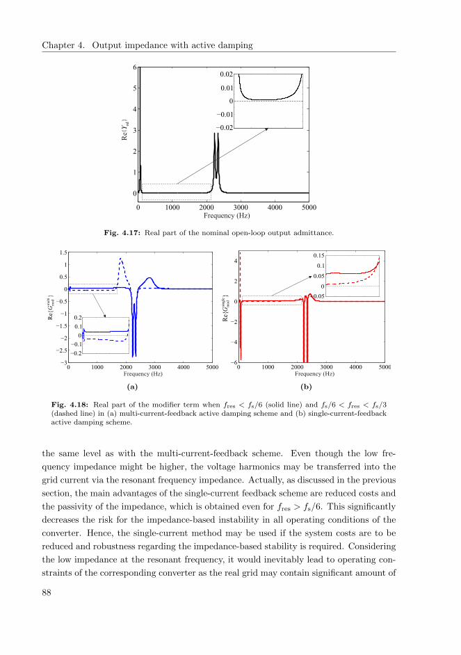
Chapter 4. Output impedance with active damping
Fig. 4.17: Real part of the nominal open-loop output admittance.
(a) (b)
Fig. 4.18: Real part of the modifier term when fres < fs/6 (solid line) and fs/6 < fres < fs/3(dashed line) in (a) multi-current-feedback active damping scheme and (b) single-current-feedbackactive damping scheme.
the same level as with the multi-current-feedback scheme. Even though the low fre-
quency impedance might be higher, the voltage harmonics may be transferred into the
grid current via the resonant frequency impedance. Actually, as discussed in the previous
section, the main advantages of the single-current feedback scheme are reduced costs and
the passivity of the impedance, which is obtained even for fres > fs/6. This significantly
decreases the risk for the impedance-based instability in all operating conditions of the
converter. Hence, the single-current method may be used if the system costs are to be
reduced and robustness regarding the impedance-based stability is required. Considering
the low impedance at the resonant frequency, it would inevitably lead to operating con-
straints of the corresponding converter as the real grid may contain significant amount of
88

4.3. Conclusions
voltage harmonics especially in multi-parallel inverter systems [47, 58]. Thus, the multi-
current scheme is better in terms of the mitigation capability of harmonic voltages as
well as internal system stability, which was shown in the root trajectory analysis in Sec-
tion 3.5. Furthermore, the real capacitor-current is measured, which allows more robust
operation, when fres > fs/6.
89

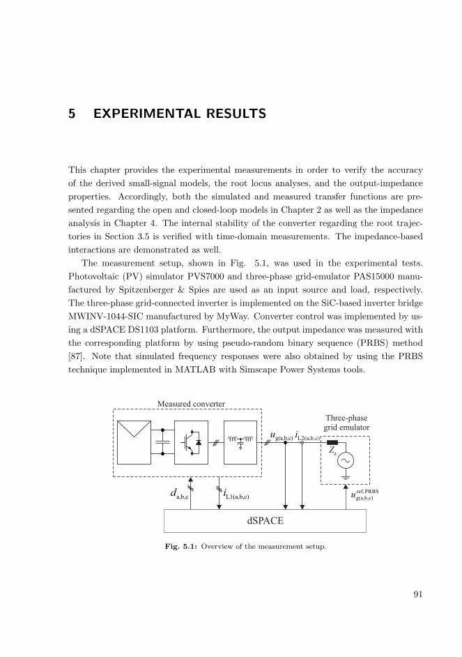
5 EXPERIMENTAL RESULTS
This chapter provides the experimental measurements in order to verify the accuracy
of the derived small-signal models, the root locus analyses, and the output-impedance
properties. Accordingly, both the simulated and measured transfer functions are pre-
sented regarding the open and closed-loop models in Chapter 2 as well as the impedance
analysis in Chapter 4. The internal stability of the converter regarding the root trajec-
tories in Section 3.5 is verified with time-domain measurements. The impedance-based
interactions are demonstrated as well.
The measurement setup, shown in Fig. 5.1, was used in the experimental tests.
Photovoltaic (PV) simulator PVS7000 and three-phase grid-emulator PAS15000 manu-
factured by Spitzenberger & Spies are used as an input source and load, respectively.
The three-phase grid-connected inverter is implemented on the SiC-based inverter bridge
MWINV-1044-SIC manufactured by MyWay. Converter control was implemented by us-
ing a dSPACE DS1103 platform. Furthermore, the output impedance was measured with
the corresponding platform by using pseudo-random binary sequence (PRBS) method
[87]. Note that simulated frequency responses were also obtained by using the PRBS
technique implemented in MATLAB with Simscape Power Systems tools.
Fig. 5.1: Overview of the measurement setup.
91

Chapter 5. Experimental results
100
101
102
103
104
−40−20
0204060
Mag
nitu
de (
dB)
100
101
102
103
104
−360−270−180−90
090
180
Pha
se (
deg)
Frequency (Hz)
Fig. 5.2: Simulated (solid line) and modeled (dotted line) open-loop control-to-inductor-currentGcL-d response in case of multi-current-feedback active damping.
5.1 Open-loop verifications
The open-loop dynamics are verified by simulations with MATLAB, which is an efficient
way to verify the open-loop models. The validity of the open-loop transfer functions is
important since the analysis in this thesis is based on the active-damping-affected open-
loop dynamics. A PRBS method is utilized to extract the frequency responses from the
time-domain simulation model. These open-loop simulations verify the models derived
in Chapters 2 and 3. The parameters used in the simulations are found in Table 3.1,
which are used also for the experimental measurements of the prototype inverter.
As discussed earlier, the open-loop control-to-inductor-current transfer function and
the output admittance are analyzed here. The former is used in the closed-loop control
design and the latter in the specific active damping analysis. Fig. 5.2 shows the predicted
and simulated active-damping-affected control-to-inductor-current transfer function in
case of the multi-current-feedback active damping scheme. Furthermore, the correspond-
ing frequency responses in case of the single-current-feedback scheme are shown in Fig.
5.3. The simulated and predicted frequency responses match well in both cases, and the
differences between the two schemes are clearly visible.
As discussed in Chapter 3, the open-loop output admittance changes significantly de-
pending on the active damping implementation. Accordingly, the single-current-feedback
active damping scheme induces control-loop-like properties and, therefore, the output
admittance was observed to exhibit significantly lower magnitude below the resonant
frequency. This observation is visible also in the simulations, which are presented in case
of both the multi and single-current-feedback schemes in Figs. 5.4 and 5.5, respectively.
92
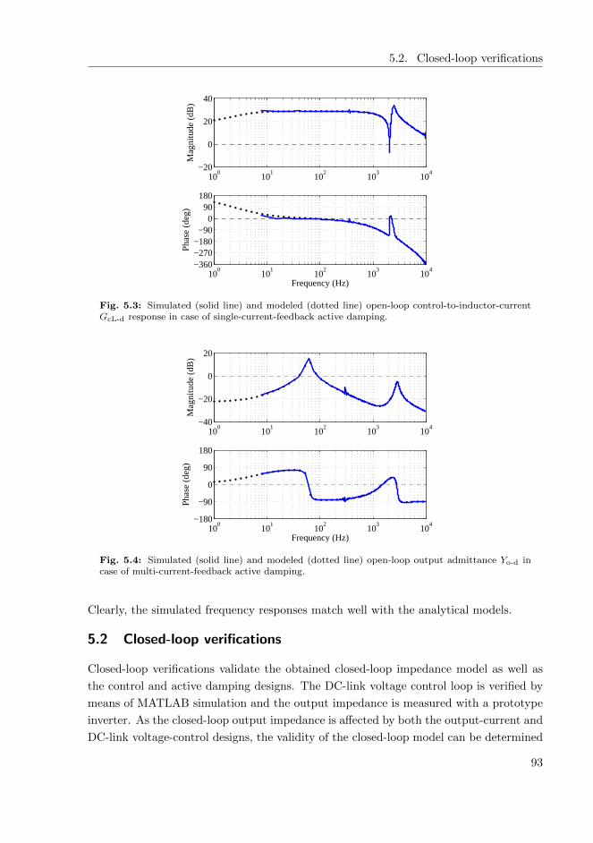
5.2. Closed-loop verifications
100
101
102
103
104
−20
0
20
40
Mag
nitu
de (
dB)
100
101
102
103
104
−360−270−180−90
090
180P
hase
(de
g)
Frequency (Hz)
Fig. 5.3: Simulated (solid line) and modeled (dotted line) open-loop control-to-inductor-currentGcL-d response in case of single-current-feedback active damping.
100
101
102
103
104
−40
−20
0
20
Mag
nitu
de (
dB)
100
101
102
103
104
−180
−90
0
90
180
Pha
se (
deg)
Frequency (Hz)
Fig. 5.4: Simulated (solid line) and modeled (dotted line) open-loop output admittance Yo-d incase of multi-current-feedback active damping.
Clearly, the simulated frequency responses match well with the analytical models.
5.2 Closed-loop verifications
Closed-loop verifications validate the obtained closed-loop impedance model as well as
the control and active damping designs. The DC-link voltage control loop is verified by
means of MATLAB simulation and the output impedance is measured with a prototype
inverter. As the closed-loop output impedance is affected by both the output-current and
DC-link voltage-control designs, the validity of the closed-loop model can be determined
93

Chapter 5. Experimental results
100
101
102
103
104
−40
−20
0
20
Mag
nitu
de (
dB)
100
101
102
103
104
−180
−90
0
90
180
Pha
se (
deg)
Frequency (Hz)
Fig. 5.5: Simulated (solid line) and modeled (dotted line) open-loop output admittance Yo-d incase of single-current-feedback active damping.
by the impedance measurements.
5.2.1 Input-voltage control design
The input-voltage control should be designed properly due to inherent constraints caused
by the used topology, which introduces an RHP pole into the control dynamics, when
operating in the CCR. Regarding the control engineering principles, the crossover fre-
quency of the control loop shall be higher than the RHP-pole frequency, which is ωpole =
Iin/CinUin ≈ 12.3 rad/s. Furthermore, the maximum limit for the crossover frequency
is imposed by the 100 Hz DC-link voltage ripple caused by an unbalanced grid. Suffi-
cient attenuation should be provided in order to avoid the pollution of the grid current
reference.
The method to verify the DC-link control loop is shown in Fig. 5.6. A sinusoidal
injection is provided to the input voltage reference signal, and the error signal as well as
the input voltage are measured. Thus, the voltage control loop is determined according to
corresponding figure as Lin = Goutci Gvc. Fig. 5.7 shows the simulated input-voltage loop
gain, where the desired 20 dB attenuation at 100 Hz is nearly obtained. Furthermore,
the gain and phase margins are 60 dB and 89 degrees, respectively, indicating good
stability margins. Moreover, difference between the simulated and predicted loop gains
is negligible, thus, the control design can be assumed to be accurate.
94

5.2. Closed-loop verifications
Fig. 5.6: Methodology for the input voltage loop gain measurement.
100
101
102
103
104
−60−40−20
02040
Mag
nitu
de (
dB)
100
101
102
103
104
−360
−270
−180
−90
0
90
Pha
se (
deg)
Frequency (Hz)
Fig. 5.7: Simulated (solid line) and modeled (dotted line) input-voltage loop gain.
5.2.2 Output impedance verification
This section presents the output impedance measurements from the prototype inverter.
The corresponding measurement setup is shown in Fig. C.1 in Appendix B. Considering
both the multi and single-current-feedback schemes, different active damping feedback
implementations are verified according to the analyses shown in Sections 3.5 and 3.1.2
under operating conditions of fres < fs/6, fs/6 < fres < fs/3 and fs/3 < fres < fs/2.
Multi-current-feedback scheme
Fig. 5.8 shows the measured d and q-components of the output impedance, when fres <
fs/6 with proportional active damping feedback (Rd = 10 Ω). As can be seen, the active-
type impedance is visible in the q-component at low frequencies as the phase is close to
-180 degrees, which is caused by the PLL [66]. The impedance magnitude in vicinity of
the resonant frequency is around 5 dB, which might be insufficient since 5 dB ≈ 1.8 Ω.
That is, a voltage harmonic at the corresponding frequency with only 1.8 V amplitude
95

Chapter 5. Experimental results
100
101
102
103
−20
0
20
40
60
Mag
nitu
de (
dB)
100
101
102
103
−180
−90
0
90
180
Pha
se (
deg)
Frequency (Hz)
Fig. 5.8: Modeled (dotted lines) and measured d and q-components (blue line and black dashedline) of the output impedance in case of proportional active damping feedback, Rd = 10 Ω.
would yield a harmonic current response of 1 A. Regarding the operating point, the
corresponding grid current is around 10 A and, therefore, the harmonic current would be
10 % of the nominal current.
The robustness of the converter can be improved for fres < fs/6 by using a high-
pass-filtered active damping feedback according to the analysis in Section 3.5. As shown
earlier in both the root locus and impedance analyses, the HPF induces more damped
transient response and higher output impedance magnitude. Accordingly, Fig. 5.9 shows
the output impedance for the corresponding case with Rd = 10 Ω and ωcutoff = ωres.
Comparing Figs. 5.8 and 5.9, the magnitude at the resonant frequency is increased
from 5 dB to around 15 dB ≈ 5.6 Ω by using the HPF active damping and, therefore,
significantly larger voltage harmonic at the resonant frequency would be required to
induce the same 1 A harmonic current as in Fig. 5.8.
When the sampling frequency changes as fs/6 < fres < fs/3, significant changes occur
in the output impedance. The phase begins to resemble active-type impedance (i.e., non-
passive) around the resonant frequency, which is harmful for the overall system stability.
This can be seen in Fig. 5.10, which shows the output impedance for proportional active
damping feedback with Rd = −10 Ω.
Considering Section 3.5, a low-pass filter is recommended for improving the system
stability, when the converter is operating under fs/6 < fres < fs/3. Comparing the
root trajectories in Figs. 3.19a and 3.20b, it is evident that such filter induces beneficial
properties in the current-control dynamics. Correspondingly, the low-pass-filtered active
damping feedback improves the output impedance characteristics as shown in Fig. 5.11
with Rd = −15 Ω. Clearly, the resonant behavior is effectively reduced as the magnitude
96

5.2. Closed-loop verifications
100
101
102
103
−20
0
20
40
60
Mag
nitu
de (
dB)
100
101
102
103
−180
−90
0
90
180P
hase
(de
g)
Frequency (Hz)
Fig. 5.9: Modeled (dotted lines) and measured d and q-components (blue line and black dashedline) of the output impedance in case of HPF active damping feedback, Rd = 10 Ω, ωcutoff = ωres.
100
101
102
103
−20
0
20
40
60
Mag
nitu
de (
dB)
100
101
102
103
−180−90
090
180270360450540
Pha
se (
deg)
Frequency (Hz)
Fig. 5.10: Modeled (dotted lines) and measured d and q-components (blue line and black dashedline) of the output impedance in case of proportional active damping feedback, Rd = −10 Ω.
of the output impedance (≈ 15 dB) only slightly varies within the frequency range of
1− 3 kHz. Hence, the grid-voltage harmonics do not affect the grid current significantly
in the given frequency range compared to the case of proportional feedback in Fig. 5.10.
By further changing the sampling frequency as fs/3 < fres < fs/2, a high-pass filter is
recommended to improve the system stability as well as the output impedance properties.
Fig. 5.12 shows the output impedance with high-pass-filtered active damping (Rd =
−15, ωcutoff = 0.5ωres). As can be observed, the output impedance exhibits similar
characteristics as in case of Fig. 5.11, since the magnitude stays relatively constant in
97
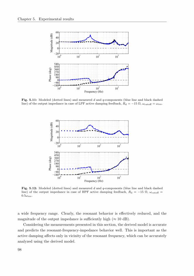
Chapter 5. Experimental results
Fig. 5.11: Modeled (dotted lines) and measured d and q-components (blue line and black dashedline) of the output impedance in case of LPF active damping feedback, Rd = −15 Ω, ωcutoff = ωres.
Fig. 5.12: Modeled (dotted lines) and measured d and q-components (blue line and black dashedline) of the output impedance in case of HPF active damping feedback, Rd = −15 Ω, ωcutoff =0.5ωres.
a wide frequency range. Clearly, the resonant behavior is effectively reduced, and the
magnitude of the output impedance is sufficiently high (≈ 10 dB).
Considering the measurements presented in this section, the derived model is accurate
and predicts the resonant-frequency-impedance behavior well. This is important as the
active damping affects only in vicinity of the resonant frequency, which can be accurately
analyzed using the derived model.
98

5.2. Closed-loop verifications
Fig. 5.13: Modeled (dotted lines) and measured d and q-components (blue line and black dashedline) of the output impedance in case of single-current-feedback active damping , Rd = 10 Ω.
Single-current-feedback scheme
Regarding the inherent operating constraints discussed in Section 3.5.3 in case of the
single-current-feedback active damping scheme, the output impedance is verified with
proportional and HPF active damping for fres < fs/6 and with HPF active damping for
fs/6 < fres < fs/3. Fig. 5.13 shows the output impedance in case of proportional active
damping with Rd = 10 Ω, when the converter operates under fres < fs/6. Evidently,
the magnitude of the output impedance in the frequency range of 100 − 1000 Hz is
higher compared to the multi-current-feedback counterpart in Fig. 5.8. This property
is beneficial as the common grid-voltage harmonics are the 3rd, 5th and 7th harmonics.
In case of the aforementioned frequencies, the output impedance in the demonstrated
case is always higher than 20 dB, which effectively prevents the voltage harmonics from
polluting the grid current.
Considering the filtered active damping feedback implementation, Fig. 5.14 shows
the output impedance in case of high-pass-filtered active damping with Rd = 15 Ω and
ωcutoff = 3ωres. Clearly, the shape of the output impedance is similar to Fig. 5.8,
since the HPF single-current-feedback active damping resembles the proportional multi-
current-feedback method. Accordingly, a decrease in the magnitude is observable in the
frequency range of 100−1000 Hz, which is peculiar in the multi-current-feedback schemes
due to the lower open-loop output admittance. Referring to the measured impedances
in Figs. 5.13 and 5.14, the analysis shown in Section 4.2 regarding the behavior of the
single-current-feedback active damping and its effect on the system transfer functions is
accurate.
99

Chapter 5. Experimental results
Fig. 5.14: Modeled (dotted lines) and measured d and q-components (blue line and black dashedline) of the output impedance in case of single-current-feedback HPF active damping , Rd = 15 Ω,ωcutoff = 3ωres.
Fig. 5.15: Modeled (dotted lines) and measured d and q-components (blue line and black dashedline) of the output impedance in case of single-current-feedback HPF active damping , Rd = 55 Ω,ωcutoff = 3.5ωres.
As discussed in Section 3.5, the measured inverter current must be high-pass filtered,
when operating under fs/6 < fres < fs/3 in order to eliminate the low frequency gain
and to induce phase boost in the active damping loop. Accordingly, Fig. 5.15 shows
the output impedance in case of HPF AD when Rd = 55 and ωcutoff = 3ωres. Signif-
icant distortions are visible in the measured impedance as the internal stability of the
converter is weak according to the root locus analysis of the corresponding case in Fig.
100
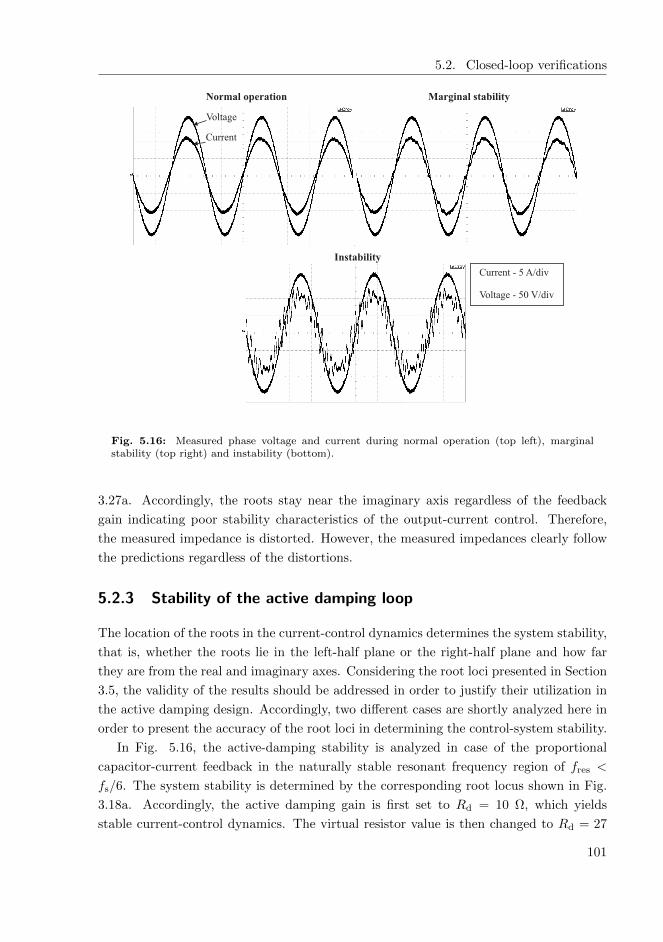
5.2. Closed-loop verifications
Fig. 5.16: Measured phase voltage and current during normal operation (top left), marginalstability (top right) and instability (bottom).
3.27a. Accordingly, the roots stay near the imaginary axis regardless of the feedback
gain indicating poor stability characteristics of the output-current control. Therefore,
the measured impedance is distorted. However, the measured impedances clearly follow
the predictions regardless of the distortions.
5.2.3 Stability of the active damping loop
The location of the roots in the current-control dynamics determines the system stability,
that is, whether the roots lie in the left-half plane or the right-half plane and how far
they are from the real and imaginary axes. Considering the root loci presented in Section
3.5, the validity of the results should be addressed in order to justify their utilization in
the active damping design. Accordingly, two different cases are shortly analyzed here in
order to present the accuracy of the root loci in determining the control-system stability.
In Fig. 5.16, the active-damping stability is analyzed in case of the proportional
capacitor-current feedback in the naturally stable resonant frequency region of fres <
fs/6. The system stability is determined by the corresponding root locus shown in Fig.
3.18a. Accordingly, the active damping gain is first set to Rd = 10 Ω, which yields
stable current-control dynamics. The virtual resistor value is then changed to Rd = 27
101

Chapter 5. Experimental results
Fig. 5.17: Measured phase voltage and current during unstable operation without HPF (top) andunder nominal operation with HPF (bottom).
Ω, where the system is marginally stable referring to the root trajectory in Fig. 3.18a.
Clearly, the output current becomes slightly distorted (cf. Fig. 5.16 top right figure).
By setting Rd = 29 Ω, the roots cross the imaginary axis to the RHP causing unstable
current dynamics as is evident in the bottom figure in Fig. 5.16.
The high-pass filter improves the system stability characteristics and allows selecting
the virtual resistor value for wider range compared to the pure proportional active-
damping-feedback implementation. This is demonstrated in Fig. 5.17 in case of the
single-current-feedback scheme when fres < fs/6. The root loci regarding the stability
analysis are shown in Figs. 3.26a and 3.26b. The pure proportional feedback is demon-
strated first, and the virtual resistor value is first set to Rd = 41 Ω, which places the
control-system poles to the RHP yielding unstable operation as visible in the top figure in
102
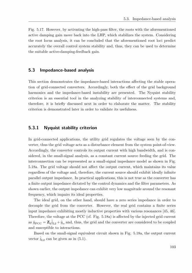
5.3. Impedance-based analysis
Fig. 5.17. However, by activating the high-pass filter, the roots with the aforementioned
active damping gain move back into the LHP, which stabilizes the system. Considering
the root locus analysis, it can be concluded that the aforementioned root loci predict
accurately the overall control system stability and, thus, they can be used to determine
the suitable active-damping-feedback gain.
5.3 Impedance-based analysis
This section demonstrates the impedance-based interactions affecting the stable opera-
tion of grid-connected converters. Accordingly, both the effect of the grid background
harmonics and the impedance-based instability are presented. The Nyquist stability
criterion is an essential tool in the analyzing stability of interconnected systems and,
therefore, it is briefly discussed next in order to elaborate the matter. The stability
criterion is demonstrated later in order to validate its usefulness.
5.3.1 Nyquist stability criterion
In grid-connected applications, the utility grid regulates the voltage seen by the con-
verter, thus the grid voltage acts as a disturbance element from the system point-of-view.
Accordingly, the converter controls its output current with high bandwidth, and is con-
sidered, in the small-signal analysis, as a constant current source feeding the grid. The
interconnection can be represented as a small-signal impedance model as shown in Fig.
5.18a. The grid voltage should not affect the output current, which maintains its value
regardless of the voltage and, therefore, the current source should exhibit ideally infinite
parallel output impedance. In practical applications, this is not true as the converter has
a finite output impedance dictated by the control dynamics and the filter parameters. As
shown earlier, the output impedance can exhibit very low magnitude around the resonant
frequency, which impairs its ideal properties.
The ideal grid, on the other hand, should have a zero series impedance in order to
decouple the grid from the converter. However, the real grid contains a finite series
input impedance exhibiting mostly inductive properties with various resonances [45, 46].
Therefore, the voltage at the PCC (cf. Fig. 5.18a) is affected by the injected grid current
as uPCC = Zg iL2 + uo and, thus, the grid and the converter are considered to be coupled
and susceptible to interactions.
Based on the small-signal equivalent circuit shown in Fig. 5.18a, the output current
vector iL2 can be given as in (5.1).
103

Chapter 5. Experimental results
(a) (b)
Fig. 5.18: (a) Small-signal representation of the grid interface and (b) its equivalent controlblock-diagram.
iL2 = is −YouPCC, uPCC = uo + Zg iL2
iL2 = is −Yo
[uo + Zg iL2
]iL2 = [I + YoZg]
−1is − [I + YoZg]
−1Youo
(5.1)
It can be seen from (5.1) that the grid current is dependent on the source current (affected
by the control dynamics) and the grid voltage. The interconnection imposes a loop
structure, which affects the behavior and stability of the grid current as demonstrated in
Fig. 5.18b.
The stability can be evaluated by applying the generalized Nyquist stability criterion
to the return-ratio matrix YoZg [88]. If the cross-couplings are neglected as they usually
are small in magnitude, since no reactive power is produced, the direct and quadra-
ture components of the impedances suffice for the analysis separately and are considered
decoupled. That is, the stability of the d-component can be analyzed with the inverse mi-
nor loop gain Lminor-dd = Yo−ddZg−dd and the q-component by Lminor-qq = Yo−qqZg−qq.
Considering Fig. 5.18b and the basic control engineering principles, the stability of the
loop is guaranteed if the converter output impedance is higher than the grid impedance
as then |Zg|/|Zo| < 1, which would ensure the stability of the corresponding minor loop
gain. Moreover, an ideal grid with zero series impedance would guarantee the stability
of the minor loop gain as well.
The real grid often exhibits inductive characteristics especially at higher frequencies
[46] and, thus the grid impedance may exceed the converter output impedance yield-
ing |Zg|/|Zo| > 1. The aforementioned case would make the converter susceptible to
impedance-based instability if the converter output impedance loses its passive charac-
teristics and the phase difference of Zg-qq and Zo-qq exceeds 180 degrees. It has been
already observed that the PLL causes active-type-impedance behavior at the low fre-
quencies [52, 58, 64, 66, 68]. Such phase behavior can exist also at higher frequencies, in
104

5.3. Impedance-based analysis
certain conditions, due to the current controller [51] and the active damping, which may
easily introduce high-frequency impedance-based instability.
5.3.2 Impedance-based instability and background harmonics
Regarding the factors affecting the stable operation of a grid-connected converter, active-
type output impedance increases significantly the impedance-based-instability sensitivity
of the grid-connected converter. Furthermore, in a grid-feeding converter, low output
impedance at the resonant frequency enables the grid voltage harmonics to interact with
the converter causing harmonic currents proportional to the impedance magnitude at
the corresponding frequency. These two factors may degrade the power quality, because
the grid current may get excessively polluted as observed, e.g., in [49]. Therefore, it
should be ensured that the output impedance of the converter exhibits passive properties
and the magnitude is as high as possible. Accordingly, it is important to address the
aforementioned risks as a part of the active damping design as its effect on the output
impedance is significant. In order to emphasize the importance of aforementioned factors,
this section will verify the power quality issues induced by the impedance-based instability
and the grid background harmonics.
Considering the impedance-based stability, active-type output impedance is analyzed
in this case, where the sampling frequency is restricted as fres > fs/6. As discussed in
Section 5.3.1, a finite series grid impedance is required for interactions. Thus, a high
impedance grid (i.e., a weak grid) is analyzed here, which is determined by the short-
circuit-ratio (SCR) or the X/R-ratio, where SCR< 3 or X/R < 5. The weak grid is
demonstrated with the resistive and inductive values of R = 0.5 Ω and L = 1 mH,
respectively, yielding X/R = 0.63.
Fig. 5.19 shows the Bode plots of the grid impedance Zg-dd and the active-type output
impedance Zodd with LPF AD, which refer to the case shown in Fig. 4.5. Moreover,
the Nyquist plot of the impedance ratio Zg-dd/Zo-dd is shown in the same figure. The
d and q-component impedances are assumed to be decoupled and, thus, the generalized
Nyquist stability criterion (GNC) is not required. In Fig. 5.19, the Nyquist plot encircles
the (−1, 0)-point when the virtual resistor value is decreased from Rd = −18 Ω to Rd =
−21 Ω indicating unstable behavior. The same phenomenon can be intuitively seen
from the Bode plots as the phase difference between Zg-dd and Zo-dd exceeds 180o when
|Zg-dd| > |Zo-dd| leading to instability. Regarding the impedance-based instability, Fig.
5.20 shows the measured output current under the violation of the Nyquist stability
criterion. Accordingly, the output current begins to oscillate at the frequency of the
violation, i.e., fharmonic ≈ 1500 Hz. As the high-frequency oscillations have been reported
from industrial photovoltaic generators [49], active damping design may have important
contribution regarding the mitigation of such harmonic oscillations and instability.
105

Chapter 5. Experimental results
Fig. 5.19: Bode plots (upper figure) for Zodd, Zg and Nyquist diagram (lower figure) for the ratioof Zg/Zodd, fres > fs/6.
The solar panels in photovoltaic power stations are not necessarily connected to a
single high-power central inverter. In fact, medium-power inverters are usually connected
in parallel (string inverters) to address the situations caused, e.g., by partial shading
conditions. In these multi-parallel inverter systems, the voltage of the point-of-common-
coupling (PCC) can be distorted due to resonant interaction between converters [18].
Thus, the PCC voltage may contain elevated harmonics near the LCL-filter resonant
frequency. This can cause oscillations in the grid current if the output impedance of the
inverter is relatively low compared to the magnitude of the oscillation. Furthermore, the
harmonic oscillation in the grid current will eventually increase the harmonic pollution
in the grid voltage due to the coupling with the grid impedance, which, in turn, will
circulate and increase the overall harmonic currents. Active damping should be, therefore,
designed to achieve as high output impedance as possible in order to prevent the grid
voltage harmonics from exciting the resonances.
The harmonic rejection capability of the converter can be analyzed by imposing a
high-frequency component in the grid voltage. In this setup, a harmonic voltage with
5 V amplitude and fharmonic = 1378 Hz was produced by the grid emulator, which
represents a grid with elevated harmonic content. In the measurements, the output
impedance magnitude of the converter is modified by adjusting the active damping gain
106
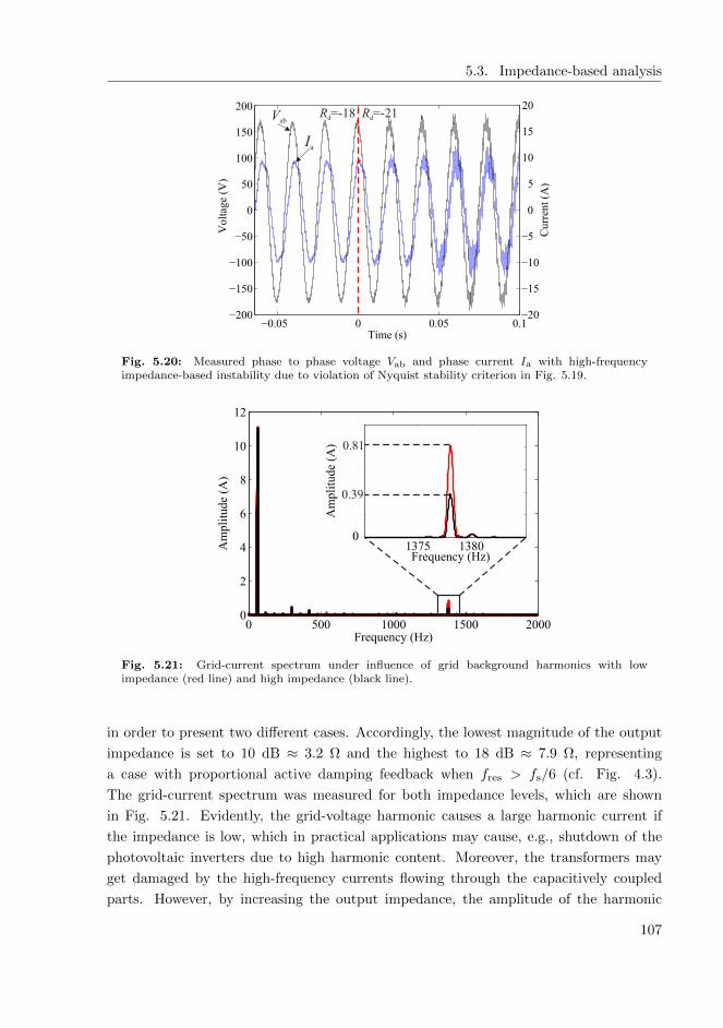
5.3. Impedance-based analysis
Fig. 5.20: Measured phase to phase voltage Vab and phase current Ia with high-frequencyimpedance-based instability due to violation of Nyquist stability criterion in Fig. 5.19.
Fig. 5.21: Grid-current spectrum under influence of grid background harmonics with lowimpedance (red line) and high impedance (black line).
in order to present two different cases. Accordingly, the lowest magnitude of the output
impedance is set to 10 dB ≈ 3.2 Ω and the highest to 18 dB ≈ 7.9 Ω, representing
a case with proportional active damping feedback when fres > fs/6 (cf. Fig. 4.3).
The grid-current spectrum was measured for both impedance levels, which are shown
in Fig. 5.21. Evidently, the grid-voltage harmonic causes a large harmonic current if
the impedance is low, which in practical applications may cause, e.g., shutdown of the
photovoltaic inverters due to high harmonic content. Moreover, the transformers may
get damaged by the high-frequency currents flowing through the capacitively coupled
parts. However, by increasing the output impedance, the amplitude of the harmonic
107

Chapter 5. Experimental results
Fig. 5.22: Grid-current waveform under influence of grid background harmonics with lowimpedance (blue line) and high impedance (red line).
current can be effectively decreased to around half of the original current. Time-domain
measurements of the corresponding case are shown in Fig. 5.22. Clearly, active damping
can be designed to provide sufficient impedance level and, therefore, the susceptibility to
the grid background harmonics is decreased.
108

6 CONCLUSIONS
This chapter presents the final conclusions regarding the thesis as well as the interesting
future research topics.
6.1 Final conclusions
Photovoltaic generator is a power-limited non-ideal current source and, thus, it imposes
peculiar design constraints on the interfacing power-electronic-based converters. Three
different operating regions, which characterize the internal dynamic of the PV cell, can
be identified as the constant-current region, constant-voltage region and the maximum
power point. These have to be considered in the analysis when deriving mathematical
models for switched-mode power converters as well as in the control system design. This
guarantees stable operation of the converter in varying operating conditions.
Multi-variable small-signal modeling was extensively applied in this thesis in order
to produce a comprehensible mathematical model for a three-phase grid-connected con-
verter. The modeling requires identification of the system input and output variables,
which subsequently affect the analysis profoundly. Therefore, it is important to assess
the dynamics of the interfaced source and load systems accurately as well. In case of
grid-connected photovoltaic inverter, the PV generator has to be considered as a current
source from the dynamic point-of-view due to its internal characteristics. Furthermore,
the load is the utility grid, which is considered as a rigid voltage source since it dictates
the voltage and frequency seen by the converter. These factors impose restrictions for
the possible controlled variables of the system. That is, the converter controls its own
input voltage in order to achieve maximum power delivery into the grid. Furthermore,
the converter controls its output current, which is synchronized with the grid by means
of the PLL. Therefore, the converter is analyzed as a current-fed-current-output system.
LCL-filter is an effective and cost-efficient way in attenuating the switching frequency
harmonics and is, therefore, widely used in practical applications. However, the inductors
and capacitance create resonant circuits causing ideally infinite or zero impedances at
certain frequencies. Accordingly, these resonances appear in the control dynamics, which
must be damped in order to achieve stable operation of the converter. Passive damping
method is a robust and simple way to damp the resonances, which is performed by
inserting a resistor usually in series with the filter capacitor. However, this will introduce
109
Chapter 6. Conclusions
additional power losses for up to 1 % and weaken the attenuation capability of the LCL-
filter. Therefore, different active damping techniques are used, which rely on modifying
the inverter control signal in order to produce the desired damping effect without any
physical components. It is shown in this thesis that both the multi and single-current-
feedback active damping schemes provide sufficient performance regarding the system
stability and impedance characteristics.
The stability of the control system regarding the active damping design was assessed
with root locus diagrams. Corresponding ICF converters lack the explicit active damping
design rules and, therefore, the aforementioned root locus plots were used to determine
the system stability. Furthermore, the root trajectories were subsequently used to analyze
their correspondence with the output impedance characteristics. Considering the active
damping design, the inherent properties of the delay were analyzed carefully as it imposes
major design constraints. Accordingly, it was observed that a low-pass filter is beneficial
when fs/6 < fres < fs/3 and, on the contrary, a high-pass filter is recommended when
fs/3 < fres < fs/2 and fres < fs/6 for improved stability characteristics. Generally, the
root locus analysis proposes that the roots should be placed as far from the imaginary-
axis as possible if high output impedance magnitude is desired. Moreover, in order to
improve the current control characteristics and stability, filtered active damping feedbacks
are recommended to be used.
As discussed in this thesis, active damping has a significant effect on the output
impedance of the converter. The output impedance determines the converter sensitivity
to external interactions and is, therefore, the key factor affecting the stability of the
grid interface. Active damping, when poorly designed, can easily compromise the stable
operation of the converter or impair the impedance characteristics. This is manifested as
extremely low magnitude in the impedance and active-type (i.e., negative real part) phase
behavior. However, by accurately considering the inherent properties of active damping,
such as delay dependency, the impedance characteristics as well as the converter stability
can be greatly improved. The stability of the grid interface can be intuitively assessed
by analyzing the frequency-domain output impedance predictions, which, on the other
hand, dictate the allowed grid impedance required for stable operation. With accurate
output impedance models, the risk for instability can be deterministically analyzed, thus
decreasing the risk for impedance-based interactions. Furthermore, the output impedance
can be used to assess the susceptibility for grid-voltage harmonics especially in vicinity
of the LCL-filter resonant frequencies.
To conclude, this thesis analyzed the effect of the active damping on system dynam-
ics and, especially, on the output impedance. Multi-variable small-signal modeling was
utilized in order to simplify the derivation of the model. This modeling technique allows
insertion of different control loops and their analysis easily. Moreover, the effect of dif-
110
6.2. Future research topics
ferent active damping feedbacks was addressed and the design guidelines regarding the
selection of correct feedback technique were presented. Accordingly, improved output
impedance characteristics can be achieved by using correct active damping design.
6.2 Future research topics
This thesis presented an accurate small-signal model of three-phase grid-connected in-
verter and its impedance properties. The effect of active damping on the system dynamics
was analyzed. However, some aspects may not have been addressed thoroughly and some
topics may need further research. Below are listed observations regarding the possible
and interesting future research topics:
• As the HPF and LPF affect significantly the stability of the converter and the shape
of the output impedance, explicit parametric design rules should be presented for
these filters. Accordingly, design criteria could be used to guarantee optimized
impedance properties for all operating conditions, i.e. fres < fs/6 and fres > fs/6.
However, due to the complexity of the small-signal modeling, explicit design criteria
may be hard to realize.
• In case of the single-current-feedback converter operating under fres > fs/6, it
should be analyzed whether the HPF is the best solution in providing suitable
stability and output impedance properties. For example, band-pass filters have
been used for ICF converters successfully in some cases and, therefore, additional
design criteria would be appreciated.
• Considering significant delay-induced constraints and differences for ICF and GCF
converters, it would be interesting to analyze and compare the active damping on
both converter control topologies regarding the output impedance. Accordingly, it
would be interesting to analyze whether one topology would be superior to another.
• The low-frequency phase flip in the d-component of the output impedance over
180 degrees is caused by the input voltage control loop and should be studied.
This behavior may impose a risk for low-frequency impedance-based instability
and should be, therefore, analyzed. It was observed that the phase flip is related
to the phase margin of the input voltage control loop, but its detailed analysis was
omitted from this thesis.
• Active damping for a grid-feeding inverter was analyzed here. However, when
islanded, the converter operates in a grid-forming mode, which leads to a different
topology and modeling details as the grid-side inductor is ’omitted’ in the analysis.
Thus, resonances in the system dynamics will change. It would be interesting to
compare active damping and output impedance characteristics of both grid-feeding
and grid-forming converters as well.
111

REFERENCES
REFERENCES
[1] B. K. Bose, “Energy, environmental pollution, and the impact of power electronics,”
IEEE Ind. Electron. Mag., pp. 6–17, Mar. 2010.
[2] “Roadmap 2050: a practical guide to a prosperous, low-carbon europe,” European
Climate Foundation (ECF), Tech. Rep., Apr. 2010.
[3] S. Valkealahti, “Forecasting the future of renewables,” in Climate Change-
Socioeconomic Effects, In Tech, Sep.. 2010, pp. 425–440.
[4] L. Nousiainen, J. Puukko, A. Maki, T. Messo, J. Huusari, J. Jokipii, J. Viinamaki,
D. T. Lobera, S. Valkealahti, and T. Suntio, “Photovoltaic generator as an input
source for power electronic converters,” IEEE Trans. Power Electron., vol. 28, no. 6,
pp. 3028–3038, Jun. 2013.
[5] L. Nousiainen, J. Puukko, and T. Suntio, “Appearance of a RHP-zero in VSI-based
photovoltaic converter control dynamics,” in IEEE INTELEC’11, Oct. 2011, pp.
1–8.
[6] T. Messo, J. Jokipii, J. Puukko, and T. Suntio, “Determining the value of DC-link
capacitance to ensure stable operation of a three-phase photovoltaic inverter,” IEEE
Trans. Power Electron., vol. 29, no. 2, pp. 665–673, Feb. 2014.
[7] J. Kivimaki, S. Kolesnik, M. Sitbon, T. Suntio, and A. Kuperman, “Design guide-
lines for multi-loop perturbative maximum power point tracking algorithms,” IEEE
Trans. Power Electron., vol. PP, no. 99, pp. 1–1, 2017.
[8] R. D. Middlebrook, “Small-signal modeling of pulse-width modulated switched-mode
power converters,” Proceedings of the IEEE, vol. 76, no. 4, pp. 343–354, Apr 1988.
[9] Y. Chen and F. Liu, “Design and control for three-phase grid-connected photovoltaic
inverter with LCL filter,” IEEE Circuits and Systems International Conference on
Testing and Diagnosis, pp. 1–4, Apr. 2009.
[10] M. Liserre, R. Teodorescu, and F. Blaabjerg, “Stability of photovoltaic and wind
turbine grid-connected inverters for a large set of grid impedance values,” IEEE
Trans. Power Electron., vol. 21, no. 1, pp. 263–272, Jan. 2006.
[11] M. Shahparasti, M. Mohamadian, and A. Yazdian, “Derivation of a stationary-frame
single-loop controller for three-phase standalone inverter supplying nonlinear loads,”
IEEE Trans. Power Electron., vol. 29, no. 9, pp. 5063–5071, Sep. 2014.
113

REFERENCES
[12] D. N. Zmood and D. G. Holmes, “Stationary frame current fegulation of PWM
inverters with zero steady-state error,” IEEE Trans. Power Electron., vol. 18, no. 3,
pp. 814–822, May 2003.
[13] Y. Jia, J. Zhao, and X. Fu,“Direct grid current control of LCL-filtered grid-connected
inverter mitigating grid voltage disturbance,” IEEE Trans. Power Electron., vol. 29,
no. 3, pp. 1532–1541, Mar. 2014.
[14] S. Jayalath and M. Hanif, “Generalized LCL-filter design algorithm for grid-
connected voltage-source inverter,” IEEE Trans. Ind. Electron., vol. 64, no. 3, pp.
1905–1915, Mar. 2017.
[15] M. Liserre, F. Blaabjerg, and S. Hansen, “Design and control of an LCL-filter-based
three-phase active rectifier,” IEEE Trans. Ind. Appl., vol. 41, no. 5, pp. 1281–1291,
Sep. 2005.
[16] B. Ren, X. Sun, S. An, X. Cao, and Q. Zhang, “Analysis and design of an LCL filter
for the three-level grid-connected inverter,” IEEE IPEMC’12, pp. 2023–2027, Jun.
2012.
[17] C. Bao, X. Ruan, X. Wang, and W. Li, “Step-by-step controller design for LCL-
type grid-connected inverter with capacitor-current-feedback active-damping,” IEEE
Trans. Power Electron., vol. 29, no. 3, pp. 1239–1253, Mar. 2014.
[18] J. L. Agorreta, M. Borrega, J. Lopez, and L. Marroyo, “Modeling and control of
N-paralleled grid-connected inverters with LCL filter coupled due to grid impedance
in pv plants,” IEEE Trans. Power Electron., vol. 26, no. 3, pp. 770–785, Mar. 2011.
[19] S. Arcuri, M. Liserre, D. Ricchiuto, T. Kerekes, and F. Blaabjerg, “Stability anal-
ysis of grid inverter LCL-filter resonance in wind or photovoltaic parks,” in IEEE
IECON’11, Nov. 2011, pp. 2499–2504.
[20] E. Twining and D. G. Holmes, “Grid current regulation of a three-phase voltage
source inverter with an LCL input filter,” IEEE Trans. Power Electron., vol. 18,
no. 3, pp. 888–895, May 2003.
[21] V. Blasko and V. Kaura, “A novel control to actively damp resonance in input LC
filter of a three-phase voltage source converter,” IEEE Trans. Ind. Appl., vol. 33,
no. 2, pp. 542–550, Mar. 1997.
[22] P. Dahono, Y. Bahar, Y. Sato, and T. Kataoka, “Damping of transient oscillations
on the output LC filter of PWM inverters by using a virtual resistor,” in Proc. IEEE
4th Int. Conf. on Power Electron. and Drive Syst., 2001, pp. 403–407.
114

REFERENCES
[23] M. Liserre, A. Dell’Aquila, and F. Blaabjerg, “Genetic algorithm-based design of the
active damping for an LCL-filter three-phase active rectifier,” IEEE Trans. Power
Electron., vol. 19, no. 1, pp. 76–86, Jan. 2004.
[24] J. Dannehl, M. Liserre, and F. W. Fuchs, “Filter-based active damping of voltage
source converters with lcl filter,” IEEE Trans. Ind. Electron., vol. 58, no. 8, pp.
3623–3633, Aug. 2011.
[25] M. Ciobotaru, A. Rosse, L. Bede, B. Karanayil, and V. G. Agelidis, “Adaptive
notch filter based active damping for power converters using LCL filters,” in IEEE
PEDG’16, Jun. 2016, pp. 1–7.
[26] J. Dannehl, C. Wessels, and F. Fuchs, “Limitations of voltage-oriented PI current
control of grid-connected PWM rectifiers with LCL filters,” IEEE Trans. Ind. Elec-
tron., vol. 56, no. 2, pp. 380–388, Feb. 2009.
[27] Y. W. Li, “Control and resonance damping of voltage-source and current-source
converters with LC filters,” IEEE Trans. Ind. Electron., vol. 56, no. 5, pp. 1511–
1521, May 2009.
[28] D. Pan, X. Ruan, C. Bao, W. Li, and X. Wang, “Optimized controller design for
LCL-type grid-connected inverter to achieve high robustness against grid-impedance
variation,” IEEE Trans. Ind. Electron., vol. 62, no. 3, pp. 1537–1547, Mar. 2014.
[29] D. Pan, S. Member, X. Ruan, S. Member, and C. Bao, “Capacitor-current-feedback
active damping with reduced computation delay for improving robustness of LCL-
type grid-connected inverter,” IEEE Trans. Power Electron., vol. 29, no. 7, pp.
3414–3427, Jul. 2014.
[30] X. Wang, C. Bao, X. Ruan, W. Li, and D. Pan, “Design considerations of digitally
controlled LCL-filtered inverter with capacitor-current-feedback active damping,”
IEEE Trans. Emerg. Sel. Topics Power Electron., vol. 2, no. 4, pp. 972–984, Dec.
2014.
[31] J. Dannehl, F. W. Fuchs, S. Hansen, and P. B. Thøgersen, “Investigation of ac-
tive damping approaches for PI-based current control of grid-connected pulse width
modulation converters with LCL filters,” IEEE Trans. Ind. Appl., vol. 46, no. 4, pp.
1509–1517, Jul. 2010.
[32] Y. Tang, P. C. Loh, P. Wang, F. H. Choo, and F. Gao, “Exploring inherent damping
characteristic of LCL-filters for three-phase grid-connected voltage source inverters,”
IEEE Trans. Power Electron., vol. 27, no. 3, pp. 1433–1443, Mar. 2012.
115

REFERENCES
[33] S. G. Parker, B. P. McGrath, and D. G. Holmes, “Regions of active damping control
for LCL filters,” IEEE Trans. Ind. Appl., vol. 50, no. 1, pp. 424–432, Jan. 2014.
[34] J. Wang, J. D. Yan, L. Jiang, and J. Zou, “Delay-dependent stability of single-loop
controlled grid-connected inverters with LCL filters,” IEEE Trans. Power Electron.,
vol. 31, no. 1, pp. 743–757, Jan. 2016.
[35] X. Li, X. Wu, Y. Geng, X. Yuan, C. Xia, and X. Zhang, “Wide damping region
for LCL-type grid-connected inverter with an improved capacitor-current-feedback
method,” IEEE Trans. Power Electron., vol. 30, no. 9, pp. 5247–5259, Sep. 2015.
[36] X. Wang, F. Blaabjerg, and P. C. Loh, “Grid-current-feedback active damping for
LCL resonance in grid-connected voltage source converters,” IEEE Trans. Power
Electron., vol. 31, no. 1, pp. 213 – 223, Jan. 2015.
[37] S. G. Parker, B. P. McGrath, and D. G. Holmes, “Regions of active damping control
for LCL filters,” IEEE Trans. Ind. Appl., vol. 50, no. 1, pp. 424–432, Jan. 2014.
[38] C. Bao, X. Ruan, X. Wang, W. Li, D. Pan, and K. Weng, “Step-by-step controller
design for LCL-type grid-connected inverter with capacitor-current-feedback active-
damping,” IEEE Trans. Power Electron., vol. 29, no. 3, pp. 1239–1253, Mar. 2014.
[39] C. Zou, B. Liu, S. Duan, and R. Li, “Influence of delay on system stability and
delay optimization of grid-connected inverters with LCL filter,” IEEE Trans. Ind.
Informat., vol. 10, no. 3, pp. 1775–1784, Aug. 2014.
[40] Y. Lyu, H. Lin, and Y. Cui, “Stability analysis of digitally controlled LCL-type grid-
connected inverter considering the delay effect,” IET Power Electron., vol. 8, no. 9,
pp. 1651–1660, Mar. 2015.
[41] J. Yin, S. Duan, and B. Liu, “Stability analysis of grid-connected inverter wth LCL
filter adopting a digital single-loop controller with inherent damping characteristic,”
IEEE Trans. Ind. Informat., vol. 9, no. 2, pp. 1104–1112, May 2013.
[42] X. Zhang, J. W. Spencer, and J. M. Guerrero, “Small-signal modeling of digitally
controlled grid-connected inverters with LCL filters,” IEEE Trans. Ind. Electron.,
vol. 60, no. 9, pp. 3752–3765, Sep. 2013.
[43] J. Xu, S. Xie, J. Kan, and L. Ji, “An improved inverter-side current feedback control
for grid-connected inverters with LCL filters,” in IEEE ICPE- ECCE’15 Asia, 2015,
pp. 984–989.
116

REFERENCES
[44] J. Xu, S. Xie, and T. Tang, “Active damping-based control for grid-connected lcl
-filtered inverter with injected grid current feedback only,” IEEE Trans. Ind. Elec-
tron., vol. 61, no. 9, pp. 4746–4758, Sep. 2014.
[45] S. Zhang, S. Jiang, X. Lu, B. Ge, and F. Z. Peng, “Resonance issues and damping
techniques for grid-connected inverters with long transmission cable,” IEEE Trans.
Power Electron., vol. 29, no. 1, pp. 110–120, Jan. 2014.
[46] L. Jessen and F. W. Fuchs, “Modeling of inverter output impedance for stability
analysis in combination with measured grid impedances,” in IEEE PEDG’15, Jun.
2015, pp. 1–7.
[47] J. He, Y. W. Li, D. Bosnjak, and B. Harris, “Investigation and active damping
of multiple resonances in a parallel-inverter-based microgrid,” IEEE Trans. Power
Electron., vol. 28, no. 1, pp. 234–246, Jan. 2013.
[48] M. Lu, X. Wang, P. C. Loh, and F. Blaabjerg,“Resonance interaction of multiparallel
grid-connected inverters with lcl filter,” IEEE Trans. Power Electron., vol. 32, no. 2,
pp. 894–899, Feb. 2017.
[49] C. Li, “Unstable operation of photovoltaic inverter from field experiences,” IEEE
Trans. Power Del., vol. PP, no. 99, pp. 1–1, Early Access 2017.
[50] J. Sun, “Impedance-based stability criterion for grid-connected inverters,” IEEE
Trans. Power Electron., vol. 26, no. 11, pp. 3075–3078, Nov. 2011.
[51] L. Harnefors, X. Wang, A. Yepes, and F. Blaabjerg, “Passivity-based stability as-
sessment of grid-connected VSCs - An overview,” IEEE Trans. Emerg. Sel. Topics
Power Electron., vol. 4, no. 1, pp. 116 – 125, Mar. 2016.
[52] B. Wen, D. Boroyevich, R. Burgos, P. Mattavelli, and Z. Shen, “Analysis of D-Q
small-signal impedance of grid-tied inverters,” IEEE Trans. Power Electron., vol. 31,
no. 1, pp. 675–687, Jan. 2016.
[53] X. Wu, X. Li, X. Yuan, and Y. Geng, “Grid harmonics suppression scheme for LCL-
type grid-connected inverters based on output admittance revision,” IEEE Trans.
Sustain. Energy, vol. 6, no. 2, pp. 411–421, Apr. 2015.
[54] D. Yang, X. Ruan, and H. Wu, “Impedance shaping of the grid-connected inverter
with LCL filter to improve its adaptability to the weak grid condition,” IEEE Trans.
Power Electron., vol. 29, no. 11, pp. 5795–5805, Nov. 2014.
117

REFERENCES
[55] X. Chen, Y. Zhang, S. Wang, J. Chen, and C. Gong, “Impedance-phased dynamic
control method for grid-connected inverters in a weak grid,” IEEE Trans. Power
Electron., vol. PP, no. 99, pp. 1–1, Early Access. 2016.
[56] M. Cespedes and J. Sun, “Impedance modeling and analysis of grid-connected
voltage-source converters,” IEEE Trans. Power Electron., vol. 29, no. 3, pp. 1254–
1261, Mar. 2014.
[57] Y. Yu, H. Li, and Z. Li, “Impedance modeling and stability analysis of lcl-type
grid-connected inverters with different current sampling schemes,” in IEEE IPEMC-
ECCE’16 Asia, May 2016, pp. 974–981.
[58] Y. Wang, X. Chen, Y. Zhang, J. Chen, and C. Gong, “Impedance modeling of three-
phase grid-connected inverters and analysis of interaction stability in grid-connected
system,” in IEEE IPEMC-ECCE’16 Asia, May 2016, pp. 3606–3612.
[59] Z. Liu, J. Liu, X. Hou, Q. Dou, D. Xue, and T. Liu, “Output impedance modeling
and stability prediction of three-phase paralleled inverters with master-slave sharing
scheme based on terminal characteristics of individual inverters,” IEEE Trans. Power
Electron., vol. 31, no. 7, pp. 5306–5320, Jul. 2016.
[60] X. Wang, Y. W. Li, F. Blaabjerg, and P. C. Loh, “Virtual-impedance-based control
for voltage-source and current-source converters,” IEEE Trans. Power Electron.,
vol. 30, no. 12, pp. 7019–7037, Dec. 2015.
[61] L. Harnefors, M. Bongiorno, and S. Lundberg, “Input-admittance calculation and
shaping for controlled voltage-source converters,” IEEE Trans. Ind. Electron.,
vol. 54, no. 6, pp. 3323–3334, Dec 2007.
[62] Y. Song, X. Wang, and F. Blaabjerg, “Impedance-based high-frequency resonance
analysis of dfig system in weak grids,” IEEE Trans. Power Electron., vol. 32, no. 5,
pp. 3536–3548, May 2017.
[63] D. Yang, X. Ruan, and H. Wu, “Impedance shaping of the grid-connected inverter
with LCL filter to improve its adaptability to the weak grid condition,” IEEE Trans.
Power Electron., vol. 29, no. 11, pp. 5795–5805, Nov. 2014.
[64] B. Wen, D. Dong, D. Boroyevich, R. Burgos, P. Mattavelli, and Z. Shen,“Impedance-
based analysis of grid-synchronization stability for three-phase paralleled convert-
ers,” IEEE Trans. Power Electron., vol. 31, no. 1, pp. 26–38, Jan. 2016.
[65] X. Wu, X. Li, X. Yuan, and Y. Geng, “Grid harmonics suppression scheme for LCL-
type grid-connected inverters based on output admittance revision,” IEEE Trans.
Sustain. Energy, vol. 6, no. 2, pp. 411–421, Apr. 2015.
118
REFERENCES
[66] T. Messo, J. Jokipii, A. Makinen, and T. Suntio, “Modeling the grid synchronization
induced negative-resistor-like behavior in the output impedance of a three-phase
photovoltaic inverter,” in IEEE PEDG’13, Jul. 2013, pp. 1–7.
[67] K. M. Alawasa, Y. A. R. I. Mohamed, and W. Xu, “Active mitigation of subsyn-
chronous interactions between pwm voltage-source converters and power networks,”
IEEE Trans. Power Electron., vol. 29, no. 1, pp. 121–134, Jan. 2014.
[68] B. Wen, D. Dong, D. Boroyevich, R. Burgos, P. Mattavelli, and Z. Shen,“Impedance-
based analysis of grid-synchronization stability for three-phase paralleled convert-
ers,” IEEE Trans. Power Electron., vol. 31, no. 1, pp. 26–38, Jan. 2016.
[69] H. Bai, X. Wang, and F. Blaabjerg, “Passivity enhancement in RES based power
plant with paralleled grid-connected inverters ,” in IEEE ECCE’16, Sep. 2016, pp.
72–72.
[70] L. Harnefors, A. G. Yepes, A. Vidal, and J. Doval-Gandoy,“Passivity-based stabiliza-
tion of voltage-source converters equipped with lcl input filters,” in IEEE IECON’14,
Oct. 2014, pp. 1700–1706.
[71] L. Harnefors, L. Zhang, and M. Bongiorno, “Frequency-domain passivity-based cur-
rent controller design,” IET Power Electron., vol. 1, no. 4, pp. 455–465, Dec. 2008.
[72] Q. Qian, S. Xie, L. Huang, J. Xu, Z. Zhang, and B. Zhang, “Harmonic suppression
and stability enhancement for parallel multiple grid-connected inverters based on
passive inverter output impedance,” IEEE Trans. Ind. Electron., vol. 64, no. 9, pp.
7587–7598, Sep. 2017.
[73] F. D. Freijedo, D. Dujic, and J. A. Marrero-Sosa, “Design for passivity in the z-
domain for LCL grid-connected converters,” in IEEE IECON’16, Oct. 2016, pp.
7016–7021.
[74] J. He and Y. W. Li, “Generalized closed-loop control schemes with embedded virtual
impedances for voltage source converters with LC or LCL filters,” IEEE Trans.
Power Electron., vol. 27, no. 4, pp. 1850–1861, Apr. 2012.
[75] Y. Li, P. Jia, and T. Q. Zheng, “Active damping method to reduce the output
impedance of the dc-dc converters,” IET Power Electron., vol. 8, no. 1, pp. 88–95,
Aug. 2015.
[76] L. Harnefors, “Modeling of three-phase dynamic systems using complex transfer
functions and transfer matrices,” IEEE Trans. Ind. Electron., vol. 54, no. 4, pp.
2239–2248, Aug 2007.
119

REFERENCES
[77] P. M. Dalton and V. J. Gosbell, “A study of induction motor current control using
the complex number representation,” in IEEE Industry Applications Society Annual
Meeting, vol. 1, Oct. 1989, pp. 355–361.
[78] A. Aapro, T. Messo, and T. Suntio, “An accurate small-signal model of a three-phase
VSI-based photovoltaic inverter with LCL-filter,” in IEEE ICPE- ECCE’15 Asia,
2015, pp. 2267–2274.
[79] I. Cvetkovic, M. Jaksic, D. Boroyevich, P. Mattavelli, F. Lee, Z. Shen, S. Ahmed,
and D. Dong, “Un-terminated, low-frequency terminal-behavioral dq model of three-
phase converters,” in IEEE ECCE’11, 2011, pp. 791–798.
[80] X. Wang, F. Blaabjerg, and P. C. Loh, “Virtual RC damping of LCL-filtered voltage
source converters with extended selective harmonic compensation,” IEEE Trans.
Power Electron., vol. 30, no. 9, pp. 4726–4737, Sep. 2015.
[81] R. Pena-Alzola, M. Liserre, F. Blaabjerg, R. Sebastian, J. Dannehl, and F. W. Fuchs,
“Systematic design of the lead-lag network method for active damping in LCL-filter
based three phase converters,” IEEE Trans. Ind. Informat., vol. 10, no. 1, pp. 43–52,
Feb. 2014.
[82] J. Dannehl, F. W. Fuchs, and P. B. Thøgersen, “PI state space current control of
grid-connected PWM converters with LCL filters,” IEEE Trans. Power Electron.,
vol. 25, no. 9, pp. 2320–2330, Sep. 2010.
[83] B. P. McGrath, S. G. Parker, and D. G. Holmes, “High-performance current reg-
ulation for low-pulse-ratio inverters,” IEEE Trans. Ind. Appl., vol. 49, no. 1, pp.
149–158, Jan. 2013.
[84] C. Bao, X. Ruan, X. Wang, W. Li, D. Pan, and K. Weng, “Design of injected
grid current regulator and capacitor-current-feedback active-damping for LCL-type
grid-connected inverter,” in IEEE ECCE’12, 2012, pp. 579–586.
[85] S. Buso and P. Mattavelli, Digital Control in Power Electronics. San Francisco,
CA, USA: Morgan & Claypool, 2006.
[86] R. Pena-Alzola, M. Liserre, F. Blaabjerg, M. Ordonez, and Y. Yang, “LCL-filter
design for robust active damping in grid-connected converters,” IEEE Trans. Ind.
Informat., vol. 10, no. 4, pp. 2192–2203, Nov. 2014.
[87] T. Roinila, J. Huusari, and M. Vilkko, “On frequency-response measurements of
power-electronic systems applying MIMO identification techniques,” IEEE Trans.
Ind. Electron., vol. 60, no. 11, pp. 5270–5276, Nov. 2013.
120

REFERENCES
[88] T. Messo, A. Aapro, and T. Suntio, “Generalized multivariable small-signal model
of three-phase grid-connected inverter in dq-domain,” in IEEE COMPEL’15, 2015,
pp. 1–8.
121


A MATLAB CODE FOR CF-VSI STEADY STATE
CALCULATION
%#######################################################################
% ### This MATLAB code solves the steady state for a grid-connected ###
% ### photovoltaic inverter ###
% ### Aapo Aapro, 15.5.2017 ###
%#######################################################################
% ########### Operating point ###########
% ### With parasitic elements ###
eq1=’-k1*IL2q=Ucd’
eq2=’k1*IL2d-k1*IL1d=Ucq’
eq3=’k2*IL2d+R*IL2q=Ucq’
eq4=’R*IL2d-rC*IL1d-k2*IL2q+Uod=Ucd’
eq5=’IL1d=2*Iin/(3*Dd)’
f=solve(eq1,eq2,eq3,eq4,eq5,’IL2d’,’IL2q’,’Ucd’,’Ucq’,’IL1d’)
% ### Simplified IL2d IL2q ###
eq10=’IL2d=(2*Iin*K_ild-3*Dd*R*Uod)/(3*Dd*K)’
eq11=’IL2q=-(2*Iin*K_ilq+3*Dd*Uod*Kuo)/(3*Dd*K)’
eq12=’Uin*Dd^2+rC*IL2d*Dd+IL2q*Dd*k1-2*Iin*Req/3=0’
eq13=’Dq*Uin-k1*(IL2d-2*Iin/(3*Dd))+rC*IL2q-2*Iin*k3/(3*Dd)=0’
123

Appendix A. Matlab code for CF-VSI steady state calculation
g=solve(eq10,eq11,eq12,eq13,’Dd’,’Dq’,’IL2d’,’IL2q’)
%#######################################################################
%#######################################################################
% ### Without parasitic elements ###
eq1=’-k1*IL2q=Ucd’
eq2=’k1*IL2d-k1*IL1d=Ucq’
eq3=’k2*IL2d+0*IL2q=Ucq’
eq4=’0*IL2d-0*IL1d-k2*IL2q+Uod=Ucd’
eq5=’IL1d=2*Iin/(3*Dd)’
h=solve(eq1,eq2,eq3,eq4,eq5,’IL2d’,’IL2q’,’Ucd’,’Ucq’,’IL1d’)
% ### Simplified IL2d IL2q ###
eq10=’IL2d=(2*Iin*K_ild-3*Dd*0*Uod)/(3*Dd*K)’
eq11=’IL2q=-(2*Iin*0+3*Dd*Uod*Kuo)/(3*Dd*K)’
eq12=’Uin*Dd^2+0*IL2d*Dd+IL2q*Dd*k1-2*Iin*0/3=0’
eq13=’Dq*Uin-k1*(IL2d-2*Iin/(3*Dd))+0*IL2q-2*Iin*k3/(3*Dd)=0’
y=solve(eq10,eq11,eq12,eq13,’Dd’,’Dq’,’IL2d’,’IL2q’)
%#######################################################################
%#######################################################################
% ### Now the symbolic values for Dd and Dq can be given as: ###
Dd = ((K*Req*(K_ilq*((8*Iin*Req*Uin*K^2)/3 + (8*Iin*K_ilq*Uin*K*k1)/3 -
(8*Iin*K_ild*Uin*K*rC)/3 + Kuo^2*Uod^2*k1^2 + 2*Kuo*R*Uod^2*k1*rC
+ R^2*Uod^2*rC^2)^(1/2) + 2*K*Kuo*Req*Uod + K_ilq*Kuo*Uod*k1
- 2*K_ild*Kuo*Uod*rC - K_ilq*R*Uod*rC))/(2*(K_ilq*k1 - K_ild*rC + K*Req))
+ (K_ilq*k1*(K_ilq*((8*Iin*Req*Uin*K^2)/3 + (8*Iin*K_ilq*Uin*K*k1)/3
- (8*Iin*K_ild*Uin*K*rC)/3 + Kuo^2*Uod^2*k1^2 + 2*Kuo*R*Uod^2*k1*rC
+ R^2*Uod^2*rC^2)^(1/2) + 2*K*Kuo*Req*Uod + K_ilq*Kuo*Uod*k1
124
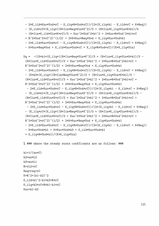
- 2*K_ild*Kuo*Uod*rC - K_ilq*R*Uod*rC))/(2*(K_ilq*k1 - K_ild*rC + K*Req))
- (K_ild*rC*(K_ilq*((8*Iin*Req*Uin*K^2)/3 + (8*Iin*K_ilq*Uin*K*k1)/3
- (8*Iin*K_ild*Uin*K*rC)/3 + Kuo^2*Uod^2*k1^2 + 2*Kuo*R*Uod^2*k1*rC
+ R^2*Uod^2*rC^2)^(1/2) + 2*K*Kuo*Req*Uod + K_ilq*Kuo*Uod*k1
- 2*K_ild*Kuo*Uod*rC - K_ilq*R*Uod*rC))/(2*(K_ilq*k1 - K_ild*rC + K*Req))
- K*Kuo*Req*Uod + K_ild*Kuo*Uod*rC + K_ilq*R*Uod*rC)/(K*K_ilq*Uin)
Dq = -((K*k1*(K_ilq*((8*Iin*Req*Uin*K^2)/3 + (8*Iin*K_ilq*Uin*K*k1)/3 -
(8*Iin*K_ild*Uin*K*rC)/3 + Kuo^2*Uod^2*k1^2 + 2*Kuo*R*Uod^2*k1*rC +
R^2*Uod^2*rC^2)^(1/2) + 2*K*Kuo*Req*Uod + K_ilq*Kuo*Uod*k1
- 2*K_ild*Kuo*Uod*rC - K_ilq*R*Uod*rC))/(2*(K_ilq*k1 - K_ild*rC + K*Req))
- (K*k3*(K_ilq*((8*Iin*Req*Uin*K^2)/3 + (8*Iin*K_ilq*Uin*K*k1)/3 -
(8*Iin*K_ild*Uin*K*rC)/3 + Kuo^2*Uod^2*k1^2 + 2*Kuo*R*Uod^2*k1*rC +
R^2*Uod^2*rC^2)^(1/2) + 2*K*Kuo*Req*Uod + K_ilq*Kuo*Uod*k1
- 2*K_ild*Kuo*Uod*rC - K_ilq*R*Uod*rC))/(2*(K_ilq*k1 - K_ild*rC + K*Req))
- (K_ild*k1*(K_ilq*((8*Iin*Req*Uin*K^2)/3 + (8*Iin*K_ilq*Uin*K*k1)/3 -
(8*Iin*K_ild*Uin*K*rC)/3 + Kuo^2*Uod^2*k1^2 + 2*Kuo*R*Uod^2*k1*rC +
R^2*Uod^2*rC^2)^(1/2) + 2*K*Kuo*Req*Uod + K_ilq*Kuo*Uod*k1
- 2*K_ild*Kuo*Uod*rC - K_ilq*R*Uod*rC))/(2*(K_ilq*k1 - K_ild*rC + K*Req))
- (K_ilq*rC*(K_ilq*((8*Iin*Req*Uin*K^2)/3 + (8*Iin*K_ilq*Uin*K*k1)/3 -
(8*Iin*K_ild*Uin*K*rC)/3 + Kuo^2*Uod^2*k1^2 + 2*Kuo*R*Uod^2*k1*rC +
R^2*Uod^2*rC^2)^(1/2) + 2*K*Kuo*Req*Uod + K_ilq*Kuo*Uod*k1
- 2*K_ild*Kuo*Uod*rC - K_ilq*R*Uod*rC))/(2*(K_ilq*k1 - K_ild*rC + K*Req))
- K*Kuo*Uod*k1 + K*Kuo*Uod*k3 + K_ild*Kuo*Uod*k1
+ K_ilq*R*Uod*k1)/(K*K_ilq*Uin)
% ### where the steady state coefficents are as follows: ###
k1=1/(ws*C)
k2=ws*L2
k3=ws*L1
R=rL2+rC
Req=req+rC
K=R^2+(k1-k2)^2
K_ild=k1^2-k1*k2+R*rC
K_ilq=k2*rC+R*k1-k1*rC
Kuo=k1-k2
125

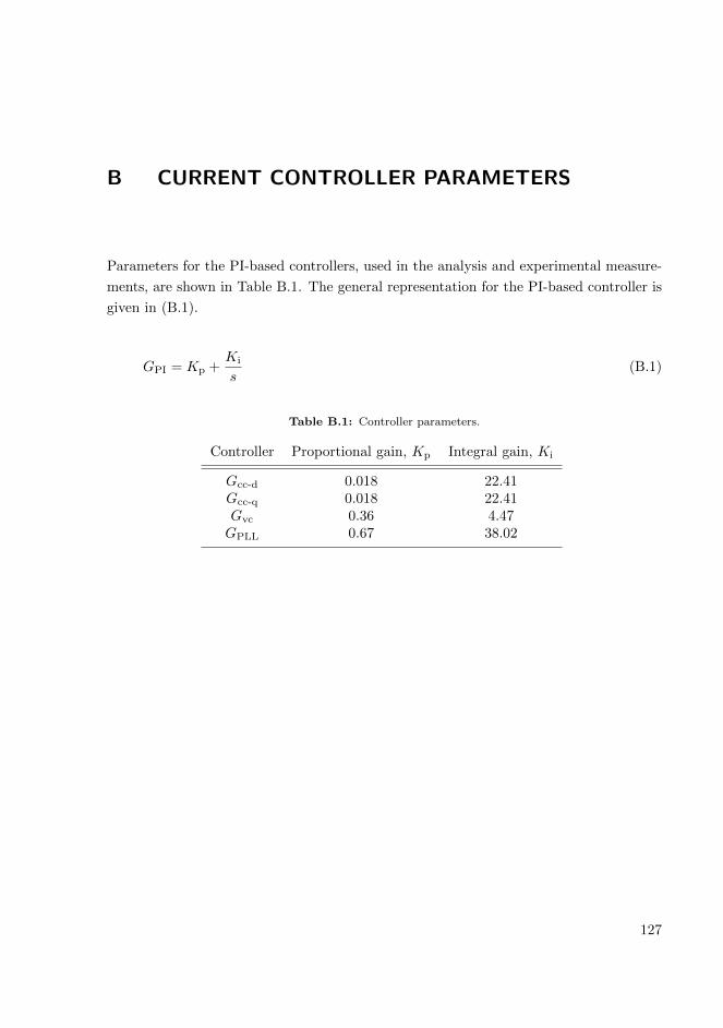
B CURRENT CONTROLLER PARAMETERS
Parameters for the PI-based controllers, used in the analysis and experimental measure-
ments, are shown in Table B.1. The general representation for the PI-based controller is
given in (B.1).
GPI = Kp +Ki
s(B.1)
Table B.1: Controller parameters.
Controller Proportional gain, Kp Integral gain, Ki
Gcc-d 0.018 22.41Gcc-q 0.018 22.41Gvc 0.36 4.47GPLL 0.67 38.02
127

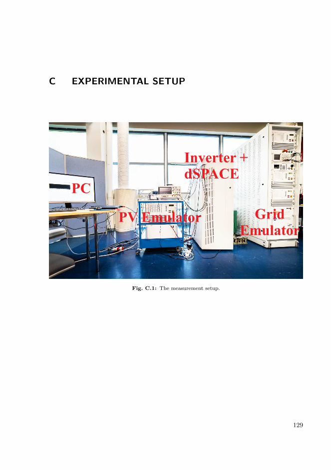
C EXPERIMENTAL SETUP
Fig. C.1: The measurement setup.
129

ISBN 978-952-15-4013-4ISSN 1459-2045
Tampereen teknillinen yliopisto PL 52733101 Tampere
Tampere University of TechnologyP.O.B. 527FI-33101 Tampere, Finland