Embed Size (px)
Citation preview
Fast Fourier Transform on a 3D FPGA
by
Elizabeth Basha
B.S. Computer Engineering, University of the Pacific 2003
Submitted to the Department of Electrical Engineering and ComputerScience
in partial fulfillment of the requirements for the degree of
Master of Science in Electrical Engineering
at the
MASSACHUSETTS INSTITUTE OF TECHNOLOGY
September 2005
@ Massachusetts Institute of Technology 2005. All rights reserved.
A uthor .......... . ... -. ----....--- --- . ..- - -Department 6tAlectrical Engineering and Computer Science
August 19, 2005
Certified by........r Krste Asanovic
Associate Professor of Electrical Engineering and Computer ScienceThesis Supervisor
Accepted by ... Arthur C. Smith
Chairman, Department Committee on Graduate Students
MASSACHUSETTS INSTITUTEOF TECHNOLOGY
MAR 2 8 2006
LIBRARIES
BARKER
----- L-.O- -


Fast Fourier Transform on a 3D FPGAby
Elizabeth Basha
Submitted to the Department of Electrical Engineering and Computer Scienceon August 19, 2005, in partial fulfillment of the
requirements for the degree ofMaster of Science in Electrical Engineering
Abstract
Fast Fourier Transforms perform a vital role in many applications from astronomy tocellphones. The complexity of these algorithms results from the many computationalsteps, including multiplications, they require and, as such, many researchers focuson implementing better FFT systems. However, all research to date focuses on thealgorithm within a 2-Dimensional architecture ignoring the opportunities available inrecently proposed 3-Dimensional implementation technologies. This project examinesFFTs in a 3D context, developing an architecture on a Field Programmable GateArray system, to demonstrate the advantage of a 3D system.
Thesis Supervisor: Krste AsanovicTitle: Associate Professor of Electrical Engineering and Computer Science


Acknowledgments
First, I would like to thank NSF for the fellowship and IBM for funding this project.Thank you to Krste Asanovic for advising me on this project and the research groupfor their friendly encouragement. Jared Casper and Vimal Bhalodia helped withvarious FPGA work and debugging some of my more interesting problems.
I would next like to thank TCC and FloodSafe Honduras for all of their supportand understanding these past couple months. ESC is an exceptional group of peo-ple; without their encouragement I would have been lost. Christine Ng and AdamNolte, your support and friendship are greatly appreciated, especially during thesisdiscussions.
Finally, thank you to my family for cheering me on throughout, commiseratingwith my frustrations, and sharing in my excitements. Mom, I would not have madeit this far without you-thank you always!
5

6

Contents
1 Introduction 13
2 Background and Related Work 152.1 FFT History and Algorithms ...... ....................... 152.2 FFT Hardware Implementations ..................... 18
2.2.1 ASIC Designs ....... ........................... 192.2.2 FPGA Designs ....... .......................... 21
2.3 3D Architectures ............................ . 22
3 System Design Description 233.1 System UTL Description . . . . . . . . . . . . . . . . . . . . . . . . . 233.2 System Micro-Architectural Description . . . . . . . . . . . . . . . . . 233.3 Four FPGA UTL Description . . . . . . . . . . . . . . . . . . . . . . 233.4 Four FPGA Micro-Architectural Description . . . . . . . . . . . . . . 253.5 Single FPGA UTL Description . . . . . . . . . . . . . . . . . . . . . 25
3.5.1 Control . . . . . . . . . . . . . . . . . . . . . . . . . . . . . . 263.5.2 FFT Datapath Block . . . . . . . . . . . . . . . . . . . . . . . 283.5.3 M em ory . . . . . . . . . . . . . . . . . . . . . . . . . . . . . . 293.5.4 Inter-FPGA Communication . . . . . . . . . . . . . . . . . . . 30
3.6 Single FPGA Micro-Architectural Description . . . . . . . . . . . . . 313.6.1 FFT Datapath Block . . . . . . . . . . . . . . . . . . . . . . . 323.6.2 Control . . . . . . . . . . . . . . . . . . . . . . . . . . . . . . 363.6.3 Memory System . . . . . . . . . . . . . . . . . . . . . . . . . . 373.6.4 Inter-FPGA Communication System . . . . . . . . . . . . . . 38
4 System Model 394.1 10 M odel . . . . . . . . . . . . . . . . . . . . . . . . . . . . . . . . . 39
4.1.1 16-point FFT . . . . . . . . . . . . . . . . . . . . . . . . . . . 394.1.2 256-point FFT . . . . . . . . . . . . . . . . . . . . . . . . . . 404.1.3 216-point FFT . . . . . . . . . . . . . . . . . . . . . . . . . . . 414.1.4 2 -20 point FFT . . . . . . . . . . . . . . . . . . . . . . . . . . . 42
4.2 Area M odel . . . . . . . . . . . . . . . . . . . . . . . . . . . . . . . . 424.3 Power M odel . . . . . . . . . . . . . . . . . . . . . . . . . . . . . . . 43
7

5 Results and Conclusions 455.1 Model Results ...... ............................... 45
5.1.1 IO M odel . . . . . . . . . . . . . . . . . . . . . . . . . . . . . 455.1.2 Area M odel . . . . . . . . . . . . . . . . . . . . . . . . . . . . 475.1.3 Power Model . . . . . . . . . . . . . . . . . . . . . . . . . .. 47
5.2 Comparison of Results to Other Systems . . . . . . . . . . . . . . . . 49
5.3 Conclusion . . . . . . . . . . . . . . . . . . . . . . . . . . . . . . . . . 51
8
List of Figures
1-1 Overall 3D FPGA Diagram ....................... 14
2-1 Example of Basic FFT Structure Consisting of Scaling and Conibina-
tional Steps . . . . . . . . . . . . . . . . . . . . . . . . . . . . . . . . 16
2-2 DIT Compared to DIF Diagram . . . . . . . . . . . . . . . . . . . . . 162-3 Radix Size Depiction . . . . . . . . . . . . . . . . . . . . . . . . . . . 172-4 FFT Calculation and Memory Flow Diagram . . . . . . . . . . . . . . 182-5 4-Step FFT Method . . . . . . . . . . . . . . . . . . . . . . . . . . . 192-6 FFT-Memory Architectures Options . . . . . . . . . . . . . . . . . . 20
3-1 System UTL Block Diagram . . . . . . . . . . . . . . . . . . . . . . . 233-2 Four FPGA UTL Block Diagram . . . . . . . . . . . . . . . . . . . . 243-3 Division among 4 Sub-Blocks . . . . . . . . . . . . . . . . . . . . . . 253-4 Four FPGA Micro-Architectural Block Diagram . . . . . . . . . . . . 26
3-5 Overall Block-Level 3D FPGA System Diagram . . . . . . . . . . . . 273-6 UTL Single FPGA System Block Diagram . . . . . . . . . . . . . . . 283-7 Micro-Architectural Single FPGA System Block Diagram . . . . . . . 32
3-8 Diagram Illustrating Iterative 4-Step Approach . . . . . . . . . . . . 333-9 16-point Block . . . . . . . . . . . . . . . . . . . . . . . . . . . . . . . 343-10 Radix4 Module with Registers . . . . . . . . . . . . . . . . . . . . . . 353-11 Fixed-Point Multiplication . . . . . . . . . . . . . . . . . . . . . . . . 36
4-1 16-point Calculation . . . . . . . . . . . . . . . . . . . . . . . . . . . 40
4-2 256-point Block . . . . . . . . . . . . . . . . . . . . . . . . . . . . . . 414-3 216-point Block . . . . . . . . . . . . . . . . . . . . . . . . . . . . . .. 414-4 220-point Block . . . . . . . . . . . . . . . . . . . . . . . . . . . . . . 43
5-1 Graph Showing the Linear Power Relationship for 2-6 FGPAs . . . . 48
9

10

List of Tables
2.1 Comparison of ASIC and FPGA FFT Implementations . . . . . . . . 21
5.1 Comparison of Results, ASIC and FPGA Implementations . . . . . . 49
5.2 Calculation Time Normalized to 16-Point Comparison . . . . . . . . . 50
5.3 Area Normalized to 16-Point Comparison . . . . . . . . . . . . . . . . 51
11

12

Chapter 1
Introduction
The Discrete Fourier Transform converts data from a time domain representation toa frequency domain representation allowing simplification of certain operations. Thissimplification makes it key to a wide range of systems from networking to imageprocessing. However, the number of operations required made the time-to-frequencyconversion computationally expensive until the development of the Fast Fourier Trans-
form (FFT), which takes advantage of inherent symmetries. The FFT still requiressignificant communication and data throughput resulting in several variations on thealgorithm and implementations. This project develops a new implementation of theFFT, improving further by developing an implementation for a 3-Dimensional FieldProgrammable Gate Array (FPGA) system.
The 3D FPGA system consists of several FPGA chips, each connected to a bank ofDynamic Random Access Memory (DRAM) chips within a single package (see Figure1-1), allowing improved communication between the FPGAs, and between a FPGAand its DRAMs. This decrease in the delay and cost of inter-chip communication in-
creases the speed of the algorithm. In addition, the use of programmable FPGA logicdecreases the implementation time as development of the algorithm and verificationcan be accomplished in-situ on the actual hardware, and increases the flexibility of
both the algorithm design and the variety of algorithms the system can run.This project focuses on large FFTs, designing a scalable 2-20 point implementation.
The FFT uses a 4-step approach to create an iterative algorithm that allows for avariable number of FPGAs. Due to the lack of manufactured 3D FPGA systems, thedesign targets a single Xilinx Virtex2 4000 chip for implementation. Based on mea-surements from this single Virtex2, a model describing the 10, area and power effectsextrapolates a multi-layer, multi-chip system using Xilinx Virtex2 Pro 40 FPGAs.This then is compared to other FPGA and ASIC FFT designs to determine theimprovements possible with 3D FFT structures.
The thesis initially introduces some background of FFT algorithms and relatedwork, followed by both a Unit-Transaction Level and a Micro-Architectural systemdescription, concluding with the multi-chip model and results.
13
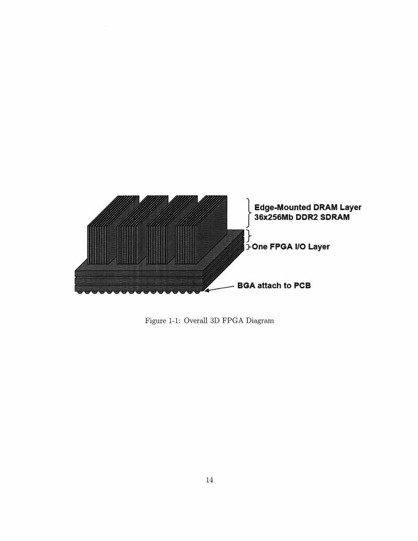
Edge-Mounted DRAM Layer36x256Mb DDR2 SDRAM
)-One FPGA I/O Layer
BGA attach to PCB
Figure 1-1: Overall 3D FPGA Diagram
14
Chapter 2
Background and Related Work
This chapter discusses the background and design points of Fast Fourier Trans-form algorithms, describes relevant hardware implementations, and concludes withan overview of 3-Dimensional implementation technologies.
2.1 FFT History and Algorithms
The Fast Fourier Transform exploits the symmetry of the Discrete Fourier Transformto recursively divide the calculation. Carl Gauss initially developed the algorithm in1805, but it faded into obscurity until 1965 when Cooley and Tukey re-developed thefirst well known version in a Mathematical Computing paper [24]. Once re-discoveredin an era of computers, people realized the speedup available and experimented withdifferent variations. Gentleman-Sande [12], Winograd [251, Rader-Brenner [21], andBruun [7] are just a few of the many variants on the FFT.
To distinguish between these different algorithms, a number of variables describean FFT algorithm, including the method of division, the size of the smallest element,the storage of the inputs and outputs of the calculation, and approach to large datasets. The basic structure of the algorithm consists of scaling steps and combinationsteps (see Figure 2-1). As will be discussed below, the order of scaling and combinationinfluences the division design decision of the algorithm as well as the storage of theinputs and outputs. The number of steps depends on the number of inputs into thealgorithm, also referred to as points and commonly represented by N, as well as thesize of the smallest element, also called the radix. The choice of approach to largedata sets affects both the radix and the division of the algorithm.
15

twiddle[O0iin[1]. ouf1].reinjO iout[1].im
twiddle[O1I
!n[2] . ouq2]srei e[2 out[2].im
twiddle[2i
Scaling Step Combinational Step Combinational Step
Figure 2-1: Example of Basic FFT Structure Consisting of Scaling and Combinational
Steps
Division Method Two methods exist to recursively divide the calculation. Math-
ematically, either the data can be divided at the time-domain input resulting in a
method called Decimation in Time (DIT) or the data can be divided at the frequency-
domain output resulting in a Decimation in Frequency (DIF) method (see Figure 2-2).
Within an algorithm, this affects where the scaling of the data occurs. A DIT al-
gorithm multiplies the inputs by the scaling factor (also know as a twiddle factor)
before combining them; a DIF multiplies after the combination.
Decdmkofin-Th ueanoi-m-n
Figure 2-2: DIT Compared to DIF Diagram
16
Ah14W VU
AAk
V _'W
4rw 4"FWF
4FW
*W
Aklaw V Ow
MW Ow VW
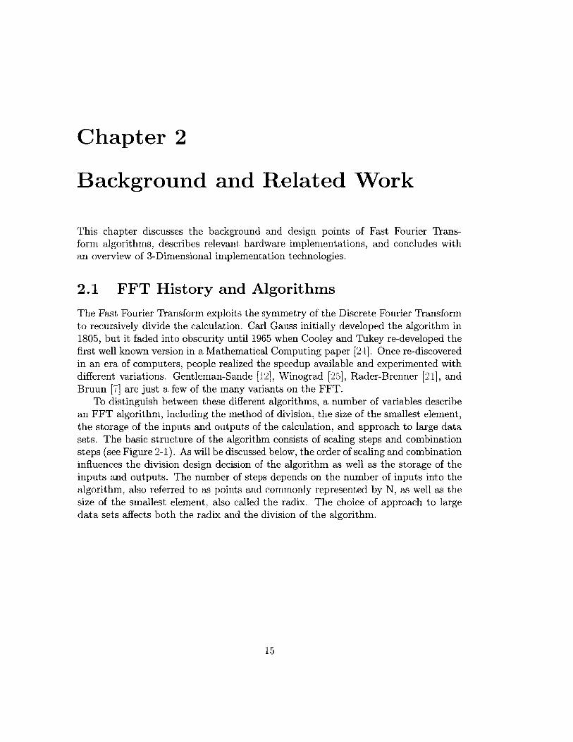
Radix Size The divisor used within the recursion defines the radix size, which inturn defines the' smallest element of the calculation. Mathematically, if an N-pointFFT is performed in radix R, the number of stages required is log( and the number
of radix nodes per stage is N, resulting in ()* ( )radix nodes for the algorithm
(see Figure 2-3). Complexity of the smallest element increases with radix size, whilethe number of multiplies decreases. Commonly power-of-two radices are used; if thenumber of inputs is odd, then mixed-radix algorithms are required increasing thecomplexity of the system.
Node Stage
N =8 pointsR=2
Stages = log(N)/Iog(R) = 3Nodes per Stage = N/R = 4
Total Nodes = Stages * Nodes per Stage = 12
Figure 2-3: Radix Size Depiction
Input and Output Storage Certain algorithms allow the same location to be read
for input and written for output. This category of in-place algorithms decreases the
storage size required, but increases the complexity especially when dealing with cus-
tom hardware. The other option doubles the amount of storage required by reading
from one location and writing to a different location (see Figure 2-4). Other consid-
erations include the stride access of the data: is the data loaded into the location so
that the algorithm can read it out unit sequentially or does the data need to be read
in stride patterns based on the radix or point size of the algorithm?
17

FFtCalculation
Step I - First Read Data Set Written by Memory
FFTCalculation
Step 3 - FFr Calculation Performed on Second Read Data Setwhile First Write Data Set Read by Memory
and New First Read Data Set Written by Memory
FFTCalculation I
Step 2 - FFT Calculation Performed on First Read Data Setwhile Second Read Data Set Written by Memory
Calculation
Step 4 - FFT Calculation Performed on First Read Data Setwhile Second Write Data Set Read by Memory
and New Second Read Data Set Written by Memory
Figure 2-4: FFT Calculation and Memory Flow Diagram
Large Data Set Approach If, as in the case of this project, the data set exceedsthe implementable FFT datapath size, two approaches can be used. First, the samealgorithm used if the datapath size was possible can be utilized by performing sec-tions of the calculation on the implementable subset of the hardware. This allows thecomputation to be scheduled in time on a small portion of the hardware. This com-plicates the scheduling and increases the complexity of generating and scheduling thescaling (or twiddle) factors for the scaling step. These design choice trade-offs lead toanother option involving changing the algorithm used to a 4-step algorithm by map-ping the 1D data set to a 2D data set (see Figure 2-5). This algorithm developed byGentleman and Sande [12] consists of viewing an N-point FFT as a (n*m)-point FFT,where N-n*m. First, n m-point FFTs are performed, covering the rows of the array.The results are multiplied by a twiddle factor, based on N, and then transposed. Stepfour involves m n-point FFTs, covering the new transposed rows of the array. This4-step algorithm reduces the amount of on-chip memory space by requiring only asubset of the twiddle factors and allows for better hardware reuse.
2.2 FFT Hardware Implementations
Past implementations focused on two different options - either to develop an algorithmfor a processor or other pre-built hardware system, or to develop new hardware,usually consisting of either an application specific integrated circuit (ASIC) design
18

KA
N, N
Sage 1 n M-point FFTs Stage 2 TWiddle Factor ScalingNN
Stage 3: Transpose Stag* 4: m n-point FFTs
Figure 2-5: 4-Step FFT Method
or, recently, an FPGA design. An FPGA design, which this project explores, allows
the hardware to focus on the specific complexities of the FFT, creating a more efficient
and faster system at a loss of generality. Although both ASIC and FPGA designs are
more customized than software algorithms, these differences in the architectures vary
due to the unique features of both implementation options.
2.2.1 ASIC Designs
ASIC designs vary greatly in size and implementation from the 64-point requirements
of a 802.11a wireless processor to the 8K needs of a COFDM digital broadcasting
system to the IM needs of a radio astronomy array. The key divisions between these
designs are the architecture of the FFT calculation and memory, the architecture of
the FFT itself, and the FFT algorithm used. As outlined in Baas [3], five options
exist for the FFT-Memory architecture: a single memory module and a single FFT
module, dual memory modules and a single FFT module, multiple pipelined memory
and FFT modules, an array of memory and FFT modules, or a cache-memory module
and a single FFT module (see Figure 2-6).
Within these options, the FFT can consist of one computational element (also
called a butterfly) performing the complete FFT serially, a stage of the butterflies
performing the computation in parallel, some pipelined combination of the two, or
splitting the calculation into two separate calculations where each can either be a
parallel or serial implementation. Gentleman and Sande introduced this latter method
known as the 4-step method as, in addition to the two calculation steps, it requires
19

FFT : Memory
A. Single FFT, Single Memory
Memory FF Memory
B. Single FFT, Dual Memory
0 0
FFT FT FF7
C. Multiple Pipelined FF1' and Memory Modules
Memory
D.Ary Memory
D. Array of FFT and Memory Modules
FFT Cache Memory
E. Single FFT, Cache-Memory Modules
Figure 2-6: FFT-Memory Architectures Options
an additional multiplication step and a transform step (see Figure 2-5, Section 2.1).Finally, the FFT algorithm used can vary widely due to the different parametersavailable (see Section 2.1).
Combinations of the above options create a wide variety of FFT ASIC implemen-tations, mostly for small FFT sizes (see Table 2.1 for a numeric view). To reducethe number of complex multiplications, Maharatna [18] implemented a 64-point FFTusing the 4-step method with no internal memory while a slightly bigger 256-pointimplementation by Cetin [8] serially reused one butterfly with ROM storage for thescaling factors and RAM storage for data. A similar 1024-point implementation byBaas [3] also used a serially pipelined element with local ROM storage, but inserteda cache between the FFT processor and the data RAM. Instead of only one butterfly,Lenart [16] unrolled the calculation and pipelined each stage with small memory be-tween stages; a larger point implementation by Bidet [6] implemented the same styleas did Park [20] although that implementation increased the bit width at each stageto reduce noise effects.
A more appropriate comparison to the proposed design is a IM FFT designed byMehrotra [19]. Their system divides into four 64-point units each consisting of radix-8 butterflies. DRAMs bracket these four units to create the complete system. Thecalculation accesses the four units four times, calculating a stage of the computation
20

Designer FFT ASIC Process Area Freq. CalculationPoints (prn) or (ASIC=mm 2, Type (ps)
FPGA Type FPGA=LUTs)Maharatna[ 18] 64 0.25 13.50 20 MHz 2174.00Cetin[8] 256 0.70 15.17 40 MHz 102.40
Baas[3] 0 3.3V 1024 0.60 24.00 173 MHz 30.00Lenart[11] 2048 0.35 ~6 76 MHz 27.00Bidet[(] 8192 0.50 1000.00 20 MHz 400.00Fuster[10] 64 Altera Apex 24320 33.54 MHz 1.91Sansaloni[23] 1024 Xilinx Virtex 626 125 MSPS 8.19
(1 CORDIC)Dillon Eng.[13] 2048 Xilinx Virtex2 9510 125 MHz 4.20RF Engines[17] 16K Xilinx Virtex2 6292 250 MSPS* 65.53Dillon Eng.[9] 512K Xilinx Virtex2 Pro 12500 80 MHz Unknown
Table 2.1: Comparison of ASIC and FPGA FFT Implementations*MSPS=MegaSamplesPerSecond
each time. 64 DRAM chips store all data with one set designated as the input to theunits and other as output during the first stage, and this designation alternating ateach latter stage.
2.2.2 FPGA Designs
Due to their more limited space and speed capabilities, FPGA designs vary slightlyless than ASIC designs, although they share the same key divisions (see Table 2.1 fora numeric comparison). Multiplications, being the most costly both in terms of arearequired and calculation time, are the common focus of optimizations. To performa 1024-point FFT, Sansaloni [23] designed a serial architecture reusing one butterflyelement with a ROM for scaling and a RAM for data storage. However, to reduce themultiplier area required, the butterfly performs the scaling at the end with a serialmultiply for both complex inputs, requiring only one multiplier instead of the usualfour. Another method for reducing the multiplication, used in Fuster [10], split the64-point calculation into two 8-point calculations, an unrolling step that requires nomultiplies within these two calculations. This 4-step algorithm does require a scalingmultiply between the two stages; however this consists of 3 multipliers compared tothe 24 necessary for the standard 64-point implementation.
Larger point FFT designs within FPGAs focus more on the overall structureof the computation. RF Engines Limited [1 7] produced a series of pipelined FFTcores using a typical approach of unrolling the complete algorithm with pipelinesat each stage of the calculation. This design is parameterizable and can computeup to 64K-point FFTs. Another company, Dillon Engineering [9] [13], approaches
large FFTs differently. Their design computes 256M-point FFTs using the 4-step
21

method. External memory stores the input, which first is transposed before enteringthe first FFT calculation. The transpose step also accesses an external SRAM fortemporary storage of some values, followed by a twiddle multiply stage and the secondFFT calculation. A final matrix transpose reorders the data and stores it in anotherexternal SRAM.
2.3 3D Architectures
Two different approaches define current 3D architectures. First, standard processesbuild the chip by creating several wafers. These wafers glue together in either a face-to-face, back-to-back or face-to-back configuration with metal vias carefully placedto connect the layers thus creating a 3D system. Another option builds a 3D systemout of existing chips, known as a Multi-Chip Module (MCM), embedding them ina glue layer with routed wires to interconnect the various modules. Production ofeither of these approaches challenges current process technologies, especially in areassuch as heat dissipation and physical design [1]. However, while waiting for processtechnologies to advance, researchers use modeling and CAD tool design to explorethe potential of 3D systems, determining the performance benefits and discussingsolutions for issues like routing between layers. Rahman [22] found that interconnectdelay can be decreased as much as 60% and power dissipation decreased up to 55%while Leeser [15] discussed a potential design for connecting the routing blocks ofone layer to another. Yet, few studies examine the architectural possibilities of 3Dsystems nor possible implementations on 3D FPGAs. Alam [2] test their layoutmethodology by simulating an 8-bit encryption processor and Isshiki [14] develops aFIR filter for their MCM technology. To begin to fill this void, this thesis examinesthe architectural possibilities and implementations of FFTs on 3D systems.
22

Chapter 3
System Design Description
This chapter describes the complete system, the system divided into four FPGAs,and a single FPGA within the system. Each description breaks down into a Unit-Transaction Level (UTL) perspective first and then the UTL translates into a micro-architectural description of hardware implemented.
3.1 System UTL Description
To understand the overall requirements of the system, a UTL description explains
what the overall system needs to do. As Figure 3-1 demonstrates, the system acceptsN complex data values, performs an FFT calculation, and outputs N complex datavalues.
Dain VMuo Cl uEft a
Figure 3-1: System UTL Block Diagram
3.2 System Micro-Architectural Description
The overall system consists of one 3D block using a Ball Grid Array (BGA) attach-ment to a Printed Circuit Board (PCB) (see Figure 1-1).
3.3 Four FPGA UTL Description
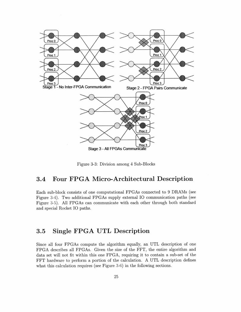
One level below this UTL describes the connections of the different sub-blocks (see
Figure 3-2). Each sub-block is identical and each computes an equal portion of the
calculation, communicating to the others via queues, with each knowing which data
23

to communicate to the others in which order such that no conflicts occur. For thepurposes of this system, the system contains four sub-blocks although, since all are
equivalent and share the calculation equally, the system as designed can work with
any number of sub-blocks. Four reasonably describes the feasible number of FPGAs
achievable with current processes and sub-divides the required calculation evenly.
I I .
N Coimplex --.Db VOWSN opJ
N Cmple N Ca.IPe
-F[,1.. N ComplexDa VWI
L -- - ---- -- -
L--- - -- - -- - -- - -
- - - - - - - - - - - -- - - - - - - - - - ->
Figur 3-:Fu PAU lc iga
igr 3- deosrtshwteagrtmdvdsaogtesbbok.Dr
in the firs stgec'u-lcI otisaloftencsaydtrqiign
external~~~ cmuicto.Tescnstgreurscmuiainbwenprsfsu-lcs whl al Iu-ok o mnct uigtefnlsae h xml
deostae how a ipeJLi- 4-on Tcndvie ih iia pten
aloin su-lok topromlrgrcluaiosi2_ontfreape
24
Proc 3Stage 1-No Inter-FPGA Commfun kation
POc 0
Proc 2
Pfoc 3Stage 3 - ANl FP~ om cate
Figure 3-3: Division among 4 Sub-Blocks
3.4 Four FPGA Micro-Architectural Description
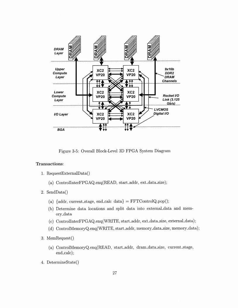
Each sub-block consists of one computational FPGAs connected to 9 DRAMs (seeFigure 3-4). Two additional FPGAs supply external IO communication paths (seeFigure 3-5). All FPGAs can communicate with each other through both standardand special Rocket JO paths.
3.5 Single FPGA UTL Description
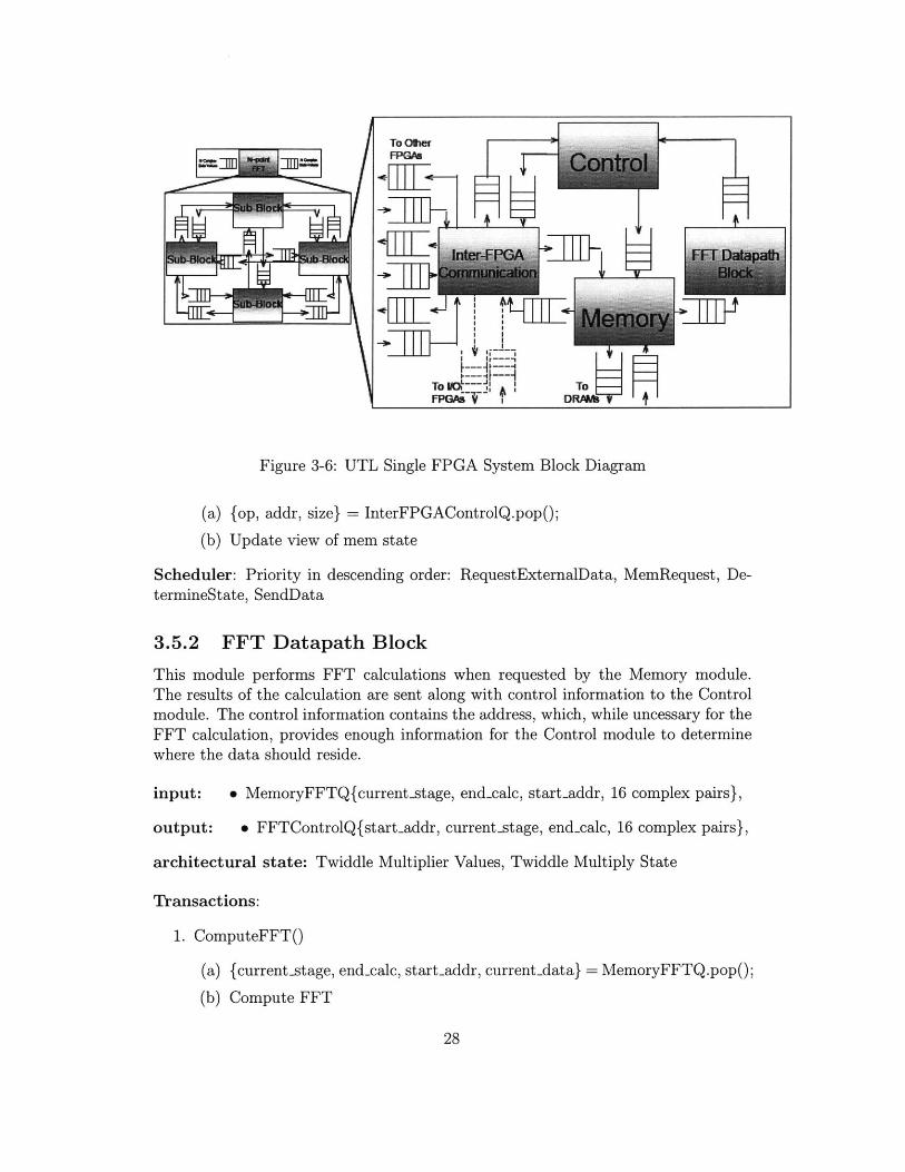
Since all four FPGAs compute the algorithm equally, an UTL description of oneFPGA describes all FPGAs. Given the size of the FFT, the entire algorithm anddata set will not fit within this one FPGA, requiring it to contain a sub-set of theFFT hardware to perform a portion of the calculation. A UTL description defineswhat this calculation requires (see Figure 3-6) in the following sections.
25
ProC 0
Proc 1
Proc 2
Stage 2 - FPGA Pairs Communicate

N Camplex
N Gunix N camplinDaia Wuer. "i V
N CM1IDabjJ Di
I Ir-r- - -
It L -L ---
- - ~- ----- ~-- -1- 16 41 1 al a r
Fi o ure: -
1.51 .nro
A. Ig k J,_ r_--r -
LL - -- --- St--y-~--ck
Tis a moul cotr thalwo dt n ntitstasatos treevsdt
a 0 aHaa s4cak
L 1 a T r -
I - I IS ~
Figure 3-4: Four FPGA Micro-Architectural Block Diagram
3.5.1 Control
This module controls the flow of data and initiates transactions. It receives data
and control packets from the FFT Module, and control packets from the Inter-FPGAmodule. Using this information as well as the current state of the calculation, themodule decides where the data should be sent, what data should be requested andthe overall state of the system, which it then translates into control and data packetsfor both the Memory and Inter-FPGA modules.
input: e FFTControlQ{addr, current-stage, end-calc, 16 complex pairs},
" InterFPGAControlQ{op, addr, size},
output: * ControlMemoryQ:{op, addr, size, current-stage, end-calc, x amount ofdata}
* ControllnterFPGAQ:{op, addr, size, x amount of data}
architectural state: Calculation State, Global Addresses
26
I I
DRAMLayer
'H0 A0
Upper XC2 XC2 9x16bCompute VP20 VP20 DDR2
Layer DRAMChannels
.......................... . ..... .. ........ ...... ..' ............ .. .. ..... ........ .. ...... ...... .... .. ... ........... ......... ..... .... ..............s ..
Lower XC2 XC2Compute VP20 VP20 Rocket I/O
Layer Link (3.125
* Le LVCMOS/0 Layer XC2 XC2 Digital 1/0
VP20 VP20
BGA T++
Figure 3-5: Overall Block-Level 3D FPGA System Diagram
Transactions:
1. RequestExternalDatao
(a) ControllnterFPGAQ.enq(READ, start-addr, ext-data.size);
2. SendDatao
(a) {addr, current-stage, endcalc data} = FFTControlQ.popo;
(b) Determine data locations and split data into external-data and mem-ory-data
(c) ControlInterFPGAQ.enq(WRITE, start-addr, ext-data-size, external-data);
(d) ControlMemoryQ.enq(WRITE, start-addr, memory-data-size, memory.data);
3. MemRequest()
(a) ControlMemoryQ.enq(READ, start-addr, dram-datasize, current.stage,end-calc);
4. DetermineStateO
27
I I
Figure 3-6: UTL Single FPGA System Block Diagram
(a) {op, addr, size} = InterFPGAControlQ.pop();
(b) Update view of mem state
Scheduler: Priority in descending order: RequestExternalData, MemRequest, De-termineState, SendData
3.5.2 FFT Datapath Block
This module performs FFT calculations when requested by the Memory module.The results of the calculation are sent along with control information to the Controlmodule. The control information contains the address, which, while uncessary for the
FFT calculation, provides enough information for the Control module to determinewhere the data should reside.
input: * MemoryFFTQ{current-stage, end-calc, start-addr, 16 complex pairs},
output: 9 FFTControlQ{start-addr, current-stage, endcal, 16 complex pairs},
architectural state: Twiddle Multiplier Values, Twiddle Multiply State
Transactions:
1. ComputeFFTO
(a) {current-stage, end-calc, startaddr, current-data} = MemoryFFTQ.popo;
(b) Compute FFT
28
To Olier
- -
To Nd -- 1 TOFPGAi7- DRAkT

(c) if (end-calc)
i. Perform Twiddle Multiplication
(d) FFTControlQ.enq(start addr, current-stage, end-calc, fft-data);
Scheduler: Priority in descending order: ComputeFFT
3.5.3 Memory
Memory controls both the Inter-FPGA memory and the DRAM, regulating the flow
of data from Inter-FPGA and Control modules into these locations and outputting
the requested blocks to either the Inter-FPGA or FFT modules as requested by the
incoming control queues.
input: * InterFPGAMemoryQ{command, addr, size, x amount of data}
" ControlMemoryQ:{op, addr, size, current-stage, endcalc, x amount ofdata}
" DRAMMemoryQ{addr, size, x amount of data}
output: * MemoryFFTQ{current-stage, endcalc, start-addr, 16 complex pairs},
" MemoryInterFPGAQ{addr, size, x amount of data},
" MemoryDRAMQ{command, addr, size, x amount of data}
architectural state: DRAM State
Transactions:
1. ExternalFPGAData()
(a) {command, addr, size, data} = InterFPGAMemoryQ.popo;
(b) if (command == READ) begin
i. if (location == DRAM) begin
A. MemoryDRAMQ.enq(READ, addr, size);
ii. end else begin
A. Read Data from Memory
iii. end
iv. MemoryInterFPGAQ.enq(addr, size, data-from-memory);
(c) end else begin
i. if (location == DRAM) begin
A. MemoryDRAMQ.enq(WRITE, addr, size, data-from-memory);
ii. end else begin
A. Write data to Memory
iii. end
29

(d) end
2. InternalFPGAData(
(a) {command, addr, size, current-stage, end-caic, data} = ControlMemo-ryQ.pop(;
(b) if (command == READ) begin
i. if (location == DRAM) begin
A. MemoryDRAMQ.enq(READ, addr, size);ii. end else begin
A. Read Data from Memory
iii. end
iv. MemoryFFTQ.enq(current-stage, endcalc, addr, dataifrom-memory);
(c) end else begin
i. if (location == DRAM) beginA. MemoryDRAMQ.enq(WRITE, addr, size, dataifrom-memory);
ii. end else begin
A. Write data to Memoryiii. end
(d) end
3. DRAMDataO
(a) {addr, size, data} = DRAMMemoryQ.pop(;
(b) Write data to Memory
Scheduler: Priority in descending order: ExternalData, InternalData
3.5.4 Inter-FPGA Communication
This module communicates to other FPGAs and outside systems. It receives datafrom any of the Control, Memory or external Inter-FPGA data queues along withcontrol information describing the data. It forwards this data to the appropriatemodule and can initiate memory transfer sequences for external Inter-FPGA modules.
input: 9 ControlInterFPGAQ:{op, addr, size, x amount of data}" OutInterFPGAQ:{command, addr, size, x amount of data}" MemoryInterFPGAQ{addr, size, x amount of data},
output: 9 InterFPGAControlQ{op, addr, size},
" InterFPGAMemoryQ{command, addr, size, x amount of data}" InterFPGAOutQ:{command, addr, size, x amount of data}
30

architectural state: None
Transactions:
1. ControlRequest()
(a) {command, addr, size, data} = ControllnterFPGAQ.pop();
(b) if (command == READ) begin
i. InterFPGAOutQ.enq(READ, addr, size);
(c) end else begin
i. InterFPGAOutQ.enq(WRITE, addr, size, data);
(d) end
2. MemRequest()
(a) {addr, size, data} = MemorylnterFPGAQ.pop();
(b) InterFPGAOutQ.enq(WRITE, addr, size, data);
3. ExternalRequest()
(a) {command, addr, size, data} = OutInterFPGAQ.popo;
(b) if (command == READ) begin
i. InterFPGAMemoryQ.enq(READ, addr, size);
(c) end else begin
i. InterFPGAMemoryQ.enq(WRITE, addr, size, data);
ii. InterFPGAControlQ.enq(WRITE, addr, size);
(d) end
Scheduler: Priority in descending order: ControlRequest, MemRequest, External-
Request
3.6 Single FPGA Micro-Architectural Description
With an UTL single FPGA description, the micro-architectural description focuseson this same one FPGA performing a portion of the calculation, requiring control,memory, and inter-fpga communication (see Figure 3-7). Each sub-system is described
below.
31

To Other Faa MS SIMp ROM di
Control
T- / Io FFTC~f1III42I
.6.1-1FT atapath Block
-Oft
FPG M y sCI
3..1 FFT Datapat Blo k~ k
The FFT Datapath Block performs a Cooley-Tukey Decimation-In-Time (DIT) al-
gorithm. This form of algorithm splits the data into subsets by even-odd patterns
and performs the twiddle calculation prior to combining data inputs. As the data
set is too large to perform the calculation, the Gentleman-Sande four-step approach
(see Section 2.1) sub-divides the larger data set. A 16-point FFT block is the largestsize that fits on the FPGA becoming the smallest factor of the 4-step algorithm. To
achieve 220, the algorithm is iterated, first generating a 16x16 or 256-point FFT, then
a 256x256 or 64K-point FFT, and finally a 64Kx16 or 220 -point FFT, all using thefundamental 16-point block (see Figure 3-8). Within the 16-point block are 8 Radix4Modules, with a separate module performing the multiplication step of the algorithm,including a sub-module providing the twiddle factors at each multiplication step of
the calculation.
FFT 16-point Block
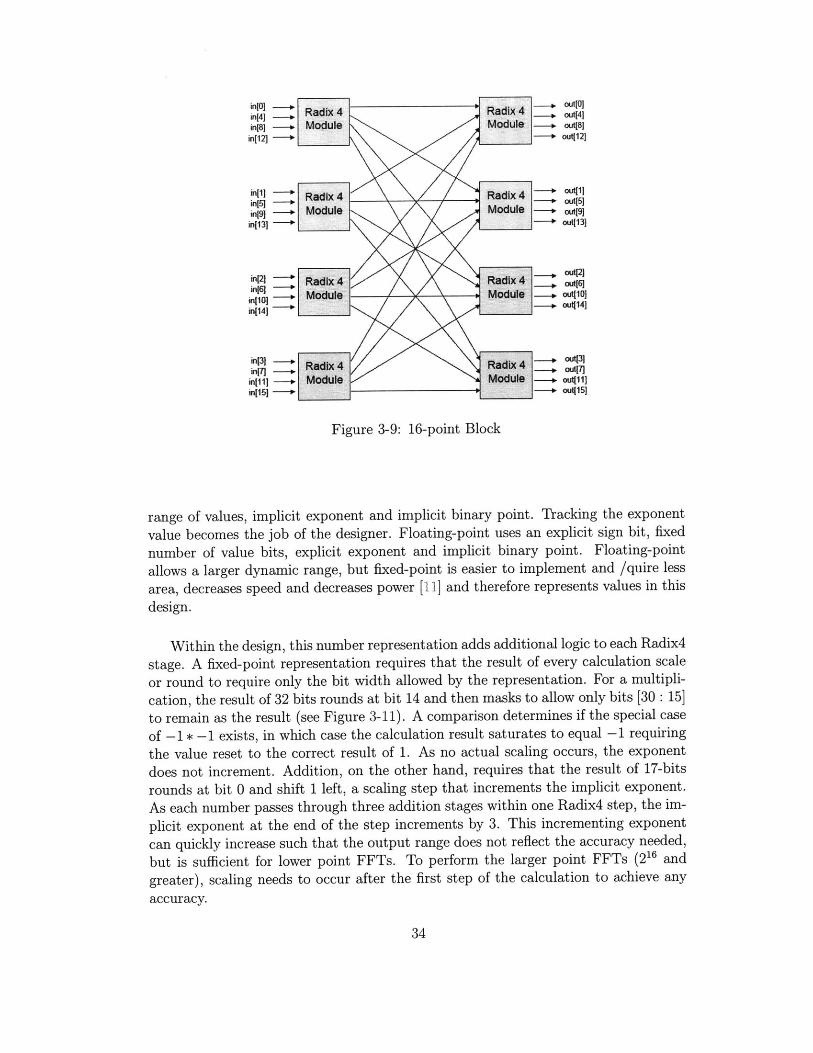
Combining the Radix4 modules creates the 16-point block. Each block consists of
two stages of 4 Radix4 nodes each (see Figure 3-9). The inputs and outputs are
32

Standard Form of 16-point FFT
Stage 1: Steps 1-3 y
Stage 2: Step 4
256-point FFT where both stages are replicated 16 times
Stage 1: Steps 1-3 Stage 2: Step 4
2"16-point FFT where both stages are replicated 256 times
Figure 3-8: Diagram Illustrating Iterative 4-Step Approach
re-ordered, as is necessary for the algorithm, implicitly in the hardware so that the input and output to the block are in natural order and both are registered. Outputs from the first stage are directly connected to the inputs of the second stage.
Radix4 Module The Radix4 Module computes an optimized version of a 4-point FFT. This consists of 3 different stages-a twiddle multiplication and two combination stages (see Figure 3-10). Each input is factored by the twiddle values, requiring 8 multiplies and 8 additions for the stage. Each of the other two stages consists of 8 additions (subtractions consist of one inversion and an addition) resulting in a total of 32 operations per module. This results in a hardware implementation that does not meet the minimum timing requirements of the hardware system requiring registers following the multiplication stage, the most time intensive step (see Figure 3-10). The multiplication stage itself implicitly uses the on-FPGA multipliers by clearly identifying these for the synthesis tools.
N umber Representation Bit width is the first design parameter for the calculation, which, for this design, matches the I8-bit width of the FPGA multipliers. In addition to this, since the calculation requires fractional values, a special number representation is required either by using fixed-point or floating-point. A fixed-point representation consists of an explicit sign bit, fixed number of bits representing a
33
inlol -* Radix 4 Radix 4 v out4J-. iModule Module -. autl8
n121 out[12]
r Radix 4 Radix 4 Mt11--. Module Module Og.n13] P -- +[u131
ir42j -0 Radix 4 Radix 4 u
-nli 0 Module Module - out[1o
'n1 0Radix 4 Radix 4 ou $
in i Otl
11l -+ ModuIO Module -0 out11]
Figure 3-9: 16-point Block
range of values, implicit exponent and implicit binary point. Tracking the exponent
value becomes the job of the designer. Floating-point uses an explicit sign bit, fixed
number of value bits, explicit exponent and implicit binary point. Floating-point
allows a larger dynamic range, but fixed-point is easier to implement and /quire less
area, decreases speed and decreases power [11] and therefore represents values in this
design.
Within the design, this number representation adds additional logic to each Radix4
stage. A fixed-point representation requires that the result of every calculation scale
or round to require only the bit width allowed by the representation. For a multipli-
cation, the result of 32 bits rounds at bit 14 and then masks to allow only bits [30 : 15]
to remain as the result (see Figure 3-11). A comparison determines if the special case
of -1 * -1 exists, in which case the calculation result saturates to equal -1 requiring
the value reset to the correct result of 1. As no actual scaling occurs, the exponent
does not increment. Addition, on the other hand, requires that the result of 17-bits
rounds at bit 0 and shift 1 left, a scaling step that increments the implicit exponent.
As each number passes through three addition stages within one Radix4 step, the im-
plicit exponent at the end of the step increments by 3. This incrementing exponent
can quickly increase such that the output range does not reflect the accuracy needed,
but is sufficient for lower point FFTs. To perform the larger point FFTs (216 and
greater), scaling needs to occur after the first step of the calculation to achieve any
accuracy.
34

inani.minrV1im
tUidd*11t
Wtkdell
in[2imin[21.mtwiddle2]MAW1dI121i
inpI vsvftl3)iMtwlem
tmm~dej3im
Scaling Step
Figure 3-10: Radix4 Moduletion.
Re is
OD+
-*OUttOIjM
-*Outfolim
.OuqfJrs-*Og41.iM
*oujajg
Combinational Step Combinational Step
with Registers. Each node represents a complex opera-
Twiddle Factor Multiplication Module
As the FFT calculation completes, each value passes through the multiplication mod-ule. If the completed calculation was the fourth step of the 4-step algorithm, the datamoves through untouched. If it was the first step, the module multiplies the value bya twiddle factor calculated by the Twiddle Factor Generation Module.
Since the 4-step algorithm is iterated, three different multiplication phases exist,one for each of the 256-point, 64K-point, and 220-point iterations. This requiresoverlapping multiplications stages such that the fourth step of the 256-point FFT isequivalent to the first step of the 64K-point FFT and, while not normally multiplied,the result of the FFT is multiplied by the twiddle factors for the 64K-point FFT.This also occurs for the fourth step of the 64K-point FFT in relation to the 22 0-pointFFT (see Figure 3-8).
Although the data is provided in parallel, the calculation occurs serially to reducethe hardware required. The data outputs serially as well, moving next to the Memorymodule.
Twiddle Factor Generation Moduletwiddle factors necessary for each stage of
Twiddle Factor Generation supplies thethe calculation. The twiddle factors follow
35
I

+
15
15
)4
+ 10 00 00 00 00 000003130 15 0oo ooo
kYe
No
Figure 3-11: Fixed-Point Multiplication
a pattern seen in the following [n, m] matrix:
WoWoWOWOW0WO
WoW1w2
W3
W4W5
Wow2
W6
W6
W10
iii
(3.1)
where W represents e-j27r/N raised to n * m where n is the row and m is the column.
Due to the repetition of values, the calculation stores only the second column val-
ues, relying on the first value to generate the first column and the following equation
[4, 19] to generate the remaining columns:
Wp* = Wp*l * Wp*(q-) (3.2)
where p is the row and q is the column of the current calculation.
This module can generate values serially, overlapping the FFT data loading cycles,
reducing the hardware costs to 4 multiplies and 4 additions, and adding no additional
latency to the calculation.
3.6.2 Control
The Control Module organizes the flow of data and the implementation of the algo-
rithm. At each step, it determines which data set to use as input, which data set to
read from memory, which twiddle factors to compute, where the output values should
be written, what the order is for write-back of the data set to memory and what is
the next stage of the calculation. It does this using a micro-code ROM and transform
36

step module.
Micro-code ROM
The Micro-code ROM controls the entire process, providing control signals and ad-
dresses for all other modules. It is implemented using on-FPGA Block RAMs.
Transform Step
Performing the third step of the algorithm requires translating the current [n, m] FFTaddress location of the data to a [iM, n] address that may be on-FPGA memory oroff-FPGA memory. The Transform Step performs this operation after the first stepof the algorithm and passes the data through after the fourth step of the algorithm,writing all data to external memory in standard order.
3.6.3 Memory System
The Memory System consists of four modules: on-FPGA Memory, FPGA Mem-ory Controller, off-FPGA DRAM, and DRAM Memory Controller; each is describedbriefly below.
FPGA Memory
Within the FPGA is 720Kb of RAM that can be programmed to be RAM, ROM orlogic modules. Most of this acts as internal RAM for the design, holding the workinginput data, the next input data, the working output data, and the past output data
set (see Figure 2-4). This allows space for the current computation while the MemoryController reads the next set of input data and writes the last set of output data.
FPGA Memory Controller
This module directs the traffic from the various locations into the FPGA Memory,organizing the memory into the different sets and connecting the on-FPGA memoryto the DRAM system.
DRAM
DRAM contains the entire input data set and store the output data set as well. Totake advantage of the number of attached DRAMs, data stripes across the DRAMs
so that 8 byte bursts access 4 inputs from each one in an interleaved manner.
DRAM Memory Controller
The DRAM Memory Controller requests data from the DRAM using a hand-shakingprotocol. Design and implementation of this module are not covered in this document.See [.] for more information.
37

3.6.4 Inter-FPGA Communication System
The Inter-FPGA Communication system transfers data blocks between FPGAs. Thecommunication pattern fixes the ordering such that no FPGAs interfere with theother's data transfer and a simple protocol provides the communication hand-shaking.
38

Chapter 4
System Model
To interpret the single FPGA results into a multi-FPGA system, a model describes
the input/output (IO), area and power effects of the number of FPGAs, the dimen-
sionality of the system, the frequency at which the system functions, and the cyclesrequired to complete one 16-point FFT. First, the model, described in terms of 10,demonstrates the iterative quality of the 4-step algorithm, which is then elaborated
into area effects and concluded with power.
4.1 10 Model
The model builds up the 220 -point system, starting with a 16-point FFT and demon-
strating how the 4-step algorithm iterates over the necessary values. At each step,the model describes the IO requirements in terms of on-FPGA RAMs, DRAMs and
external communication.
4.1.1 16-point FFT
This model assumes that the bandwidth of the inter-communication connections ex-
ceeds the bandwidth of the DRAM communication connections.
The next key bandwidth consideration is the FFT calculation itself. The following
equation represents this value:
I word bitsBFFT - f - * (32 * 16 (4.1)
C cycle word
where f is the frequency of system and C is the cycles required of 16-point FFT,decomposed into:
C = CRead + CFFT + CWrite (4.2)
Figure 4-1 displays how the calculation divides into the values CRead, CFFT, and
CWrite. This model then assumes that the DRAM connection limits the bandwidthof the system, although this connection can match the FFT bandwidth by increasing
39

the number of DRAMs used to satisfy:
D = BFFT (43)BDRAM
where D is the number of DRAMs connected to the system. The model assumes thatD DRAMs connect to the system, leaving BFFT as the dominant factor.
To better understand the connections required, Figure 4-1 demonstrates the dataaccesses needed for the 16-point calculation. No external FPGAs or DRAMS con-tribute to the data required at this stage, all data is read from one internal FPGARAM and written into another. This block then requires
Ct= -- (4.4)
ftime to complete, calculation time being our metric for the 10 analysis.
Ime
Ca = Read Fmm RAM, Cm = FFT C. = Wifte To RAM,
Figure 4-1: 16-point Calculation
4.1.2 256-point FFT
Figure 4-2 represents the 256-point FFT, composed of two stages where stage oneconsists of 16 16-point FFTs comprising the first three steps of the calculation andstage two consists of 16 16-point FFTs comprising the final step of the calculation.Again, no external FPGAs or DRAMs supply any of the data, although the accesspattern for the second stage modifies to read from RAM 2 and write into RAM 2.Completion of this block requires
St256 = 2 * 16* t16 + - (4.5)
f
where S is the cycles required to switch between stages.
40

Ime
16 16-pont FFTs 16 16-point FFTs
Stage 1 Stage 2
Figure 4-2: 256-point Block
4.1.3 2 16-point FFT
A 216-point FFT consists of two stages of 256 256-point FFTs and necessitates DRAM
connections to store the data values. As Figure 4-3 shows, because the access pattern
for the 256-point block modifies the RAMs used in the second stage of 16-point blocks,RAM1 supplies all the data and RAM2 stores all the data from the 256-point block
perspective. To ensure this pattern and pipeline the DRAM accesses, two sets of DDRAMs connect to the FPGA. DRAM1 loads data into RAM1 and DRAM 2 stores
data from RAM 2 during the first stage of the calculation, switching during the second
stage to using DRAM2 for both roles.
Ime 0
256 256-point FFTs 256 256-point FFTs
PMtaedDRAM
And RAMDRA, DR
DRM& DRA42
Stage 1
DRAM DRM
Frnish SI=eRUM DRAL49
DRAM,
Stage 2
Figure 4-3: 216-point Block
41

Loading begins concurrent with the first 256-point block, assuming that, duringthe overhead of loading the data into the DRAMs, a minimum of the first 256 complexvalues load directly into the RAM. During the last 256-point block of the first stage,data is preloaded for the second stage from the results of this block and DRAM 2.Storing stalls during the first 256-point block, commencing writing the outputs duringthe second 256-point block and finishing with the first stage during the first 256-point block of the second stage. The results of the last 256-point block of the secondstage remain in RAM 2 , inserting into the output stream of the system at the correctmoment. Completion of this block requires
S S St 2 16 = 2* 256* t 256 + - = 2* 256* (32* ti6 + )+ - (4.6)
f f f
4.1.4 221-point FFT
While either 256-point or 216 could be implemented with additional FPGAs, 22 0-pointseems the most likely size to increase the number of FPGAs (referred to as F hereafter)in the system although, as assumed in Section 4.1.1, the bandwidth of accessing theDRAMs overshadows that of transferring data between FPGAs. Instead, the stagebreakdown appears as the key variation in evaluating multi-FPGA 10. During thefirst stage, 16 21 -point blocks compute, followed by 2 16-point calculations (seeFigure 4-4). Similar to the access pattern of RAMs in the 256-point block, the firststage loads data from DRAM1 and stores to DRAM 2 , reversing the order for thesecond stage. This results in a total calculation time of
16 * t2± 216 +S 16 21 6 16 ST= *21e F t16 +-=(-*16384+-F)*tie+(513*-+1)*- (4.7)F F f F F' F'f
an equation that is solely dependent on the number of FPGAs F, the number of cyclesto switch stages S, the time to calculate one 16-point FFT t 16 , and the frequency ofthe system f.
4.2 Area Model
Area increases linearly as a function of number of FPGAs, F,
A = F * (a1FPGA + (F - 1) * aInter-FPGA) (4-8)
where a1FPGA is the area of the design on one FPGA and aInter-FPGA is the area of theInter-FPGA module. This module requests and sends data both to other FPGAs andto the DRAMs, requiring a small amount of logic and some buffers, a value estimatedbased on the implemented Inter-FPGA module and reasonable buffer sizes.
42

ime
16ff 2'68-point FFTS 2"61F 16-ont FFTs
DRAK RAF4DRNAK DRAM
TrarmfeftTranfml=
Stage I Stage 2
Figure 4-4: 220-point Block
4.3 Power Model
As the number of FPGAs increases, only the IO system contributes significantlyto the power increase. Each FPGA connects to the same number of DRAMs andperforms the same calculation, but the communication time decreases linearly with
the number of FPGAs resulting in the same power usage for the calculation and theDRAM accesses within a shorter amount of time. However, the additional Inter-FPGA modules and the 10 communication itself will require more power as thenumber of FPGAs communicating increase. Therefore, the power model focuses onthe 10 communication power.
If we assume that both 2D Multi-Chip Module (MCM) and 3D MCM technologyuse similar wire connections, the power depends on the length of the interconnect andthe bandwidth at which the interconnect operates. Just focusing on one interconnec-tion, power is:
pi = 1i * Bi (4.9)
To determine the entire interconnect power, the number of Rocket 10 compared to
LVDS connections becomes critical. As long as the Inter-FPGA bandwidth is greaterthan or equal to the DRAM bandwidth, LVDS connections can replace Rocket 10connections. However the number of DRAMs limits the number of available LVDSconnections (NLVDSA) such that
NLVDSA = NLVDS.Total - D * NLVDSDRAM (4.10)
In order to match the bandwidth requirements, D (the number of DRAMs attached
to a FPGA) LVDS connections are required. This results in a total interconnect
43
power of:
Pi = NRocket*P'iRocket+D*NLVDSA*PiLVDS = NRocket*l'Rocket*BiRocket+D*NLVDS.A*liLVDS*BiLVDS
(4.11)Total power then depends on the total interconnect power per FPGA (P) and
the number of FPGAs (F):P = P, * F (4.12)
44

Chapter 5
Results and Conclusions
This chapter first evaluates the model assumptions and analyzes the results of themodel. Then it compares the results to other ASIC and FPGA designs followed bysome conclusions.
5.1 Model Results
With the models developed and the design implemented in stages of 16-point, 256-point, 4096-point, and 2' 2 -point, we now examine the assumptions of the model andanalyze the results. As with the model development, the analysis examines first the10 model, followed by area and power.
5.1.1 10 Model
The model first assumes that the DRAM communication limits the system bandwidth.As the system contains Virtex2 Pro 40 FPGAs, two methods for external communi-cation exist, either Rocket 10 or LVDS. Rocket 10 operates the fastest achieving abandwidth of 100 Gb/s for 1 module [26) although the number of modules limits thenumber of connections to 12 for the Virtex2 Pro 40. LVDS for this system allows 804connections with a theoretical maximum of 840 Mb/s bandwidth although this modeluses an experimentally verified value of 320 Mb/s. As the number of FPGAs in onesystem is unlikely to exceed 12 in the near future, this model initially describes allcommunication between FGPAs in terms of Rocket IO connections and uses LVDSconnections for the DRAMs only. These initial 10 values result in bandwidths of:
BInter-FPGA =100-- (5.1)
BDRAM = 320 (5.2)S
Therefore the DRAM bandwidth does exceed the Inter-FPGA communication band-width. Evaluating the FFT bandwidth requires measuring the frequency (f) at which
45

the 16-point block functions and the number of cycles required for one 16-point block(C). Upon implementing this block, the resulting measurements are:
f = 93MHz (5.3)
CRead = 16cycles (5.4)
CFFT = 7cycles (5.5)
Cwrite = 16cycles (5.6)
C = CRead + CFFT + CWrite = 39cycles (5.7)
1 bits GbBFFT = f * - * 512 = 1.22 (5.8)
C cycle s
A result that also demonstrates that the DRAM limits the bandwidth and requiresone set to consist of 4 DRAMs, or 8 DRAMs attached to each FPGA, which fitswithin the 9 DRAMs allocated per FPGA.
Before evaluating the calculation time, we need to establish the validity of usingthe measurements of one 16-point block for all measurements. While the 10 modelclearly defines the use of the number of cycles as a consistent value for each stage,the frequency can depend on the implementation of the various steps within eachstage and may vary between stages, requiring anew the evaluation of the bandwidth,DRAMs connected, and 16-point block calculation time. Measurement of each im-plemented stage has not proven this the case and allows the usage of the 16-pointblock calculation time. The model also defined a parameter S, the number of cyclesrequired to switch between stages, which measures at 2 cycles. This results in:
Ct1 6 =- O.42ps (5.9)
f
St256= 2 * 16 * t16 + - = 13.44pas (5.10)
f
St 216 = 2 * 256 * (32 * t 16 ) + - = 6.88ms (5.11)
f
16 216 16 St220 =(- * 16384 + ) * t16 + ( + 1) *- = 34.39ms (5.12)
F F F fwhere the number of FPGAs (F) is 4.
46

5.1.2 Area Model
Xilinx ISE Foundation supplies area measurements during the mapping process. De-
termining 22 0 -point requires extending all the designs, whose linear size increasedemonstrates that the design will saturate the FPGA. All other design stages usethe Xilinx area numbers although determining the area of a multi-FPGA system
requires the addition of the Inter-FPGA area, measured as:
aInter-FPGA = 68LUTs (5.13)
resulting in a 4 FPGA area of
A = F * (a1FPGA + (F - 1) * aInter-FPGA) = 4 * (46000 + 3 * 68) (5.14)
5.1.3 Power Model
Power reflects the difference between a 2D and 3D design therefore our result is a ratioof the total interconnect power, which depends on the power of one interconnect, afunction of the length and bandwidth. From previous research [22][E5] [1], the ratioof 2D interconnect length to 3D interconnect length averages to:
3D = 0.80 (5.15)hi2D
Since all other factors are equal, this translates into an average 20% total interconnectpower savings or an average total power savings of 20%.
The trade-off of Rocket IO and LVDS connections affects both 2D and 3D equallyin terms of power, but highlights an interesting power design point. First, given that
NLVDSDRAM = 33 and the maximum number of Rocket 10 connections is 12, clearlythe number of LVDS connections available exceeds the number necessary.
(NLVDSTotal - D * NLVDS-DRAM) = 68 > 12 (5.16)D
This also demonstrates the relationship between the number of Rocket 10 and LVDSconnections as:
NLVDSA = ((F + 1) - NRocket) * D (5.17)
Next, we reasonably assume that liRocket = liLVDS since both connections shouldaverage the same length over the various combinations of pin locations and routingpaths. This then allows the power to reduce to a factor of the bandwidth and numberof connections alone:
P = F * (NRocket * BiRocket + D * NLVDS-A * Bi LVDS) (5.18)
Combining Equation 5.17 and Equation 5.18, varying over the number of FPGAs andRocket 10 connections, the linear relationship appears (see Figure 5-1). This demon-strates that committing all LVDS connections to both DRAM and other FPGA con-
47

nections allows significantly lower power while maintaining the bandwidth. RocketIOs then can focus on communication to the external IO specialized FPGAs, allowingfaster reading and writing of data between the system and external world. Alterna-tively, use of both LVDS and Rocket IO connections allows the number of FPGAswithin the system to increase, suggesting that an internal cluster architecture may bepossible with Rocket IOs connecting groups of internally LVDS connected FPGAs.
X Power vs. Number of Rocket Os for Varying Number of FPGAs
1 1.5 2 2.5 3 3.5 4Number of Rocket l0s
4.5 5 5.5 6
Figure 5-1: Graph Showing the Linear Power Relationship for 2-6 FGPAs
48
2.5 -
2
1.5
0.5 -
5.2 Comparison of Results to Other Systems
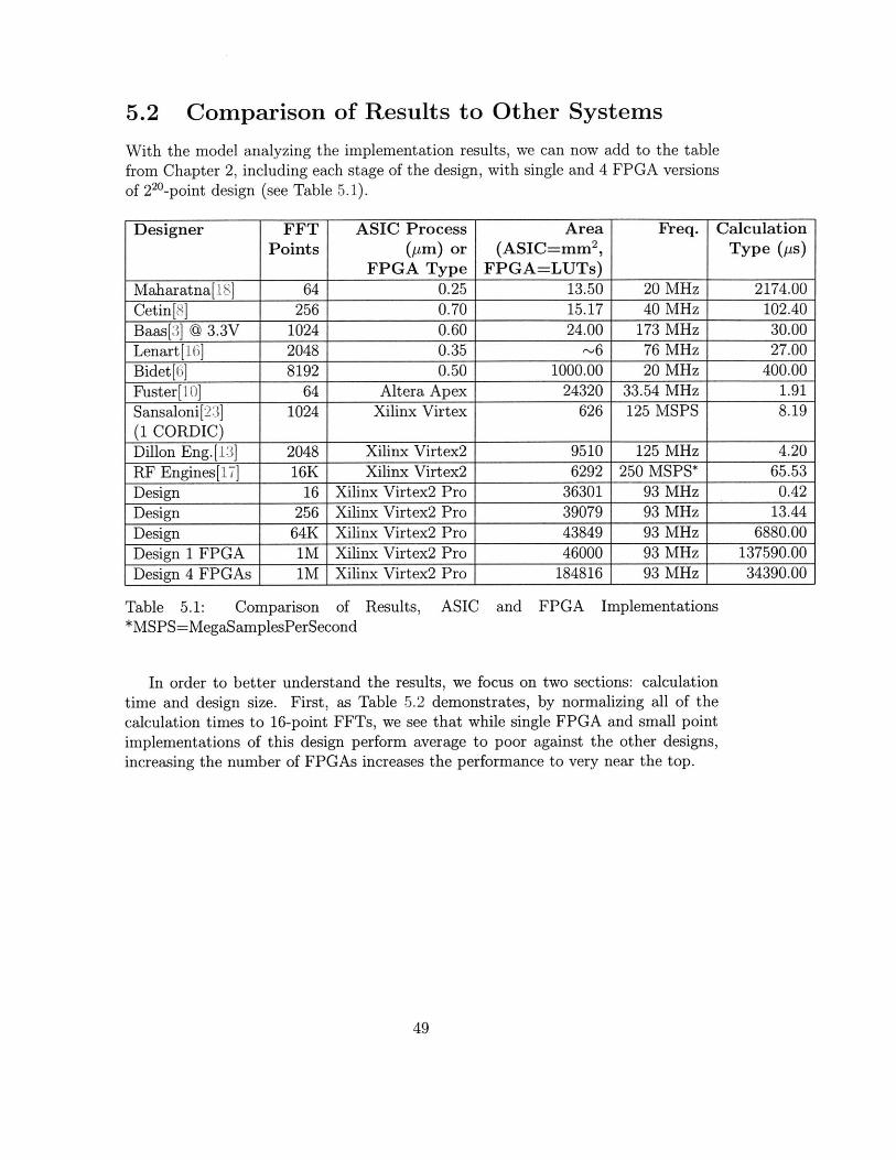
With the model analyzing the implementation results, we can now add to the tablefrom Chapter 2, including each stage of the design, with single and 4 FPGA versionsof 220 -point design (see Table 5.1).
Designer FFT ASIC Process Area Freq. CalculationPoints (pjm) or (ASIC=mm 2 , Type (ps)
FPGA Type FPGA=LUTs)Maharatna[18] 64 0.25 13.50 20 MHz 2174.00Cetin[8] 256 0.70 15.17 40 MHz 102.40
Baas[3] A 3.3V 1024 0.60 24.00 173 MHz 30.00Lenart[16] 2048 0.35 ~6 76 MHz 27.00Bidet[6] 8192 0.50 1000.00 20 MHz 400.00Fuster[.10] 64 Altera Apex 24320 33.54 MHz 1.91Sansaloni[23] 1024 Xilinx Virtex 626 125 MSPS 8.19
(1 CORDIC)Dillon Eng.[13] 2048 Xilinx Virtex2 9510 125 MHz 4.20RF Engines[ 7] 16K Xilinx Virtex2 6292 250 MSPS* 65.53
Design 16 Xilinx Virtex2 Pro 36301 93 MHz 0.42
Design 256 Xilinx Virtex2 Pro 39079 93 MHz 13.44
Design 64K Xilinx Virtex2 Pro 43849 93 MHz 6880.00Design 1 FPGA IM Xilinx Virtex2 Pro 46000 93 MHz 137590.00Design 4 FPGAs IM Xilinx Virtex2 Pro 184816 93 MHz 34390.00
Table 5.1: Comparison*MSPS=MegaSamplesPerSecond
of Results, ASIC and FPGA Implementations
In order to better understand the results, we focus on two sections: calculationtime and design size. First, as Table 5.2 demonstrates, by normalizing all of thecalculation times to 16-point FFTs, we see that while single FPGA and small pointimplementations of this design perform average to poor against the other designs,increasing the number of FPGAs increases the performance to very near the top.
49
'oil

Designer FFT Original NormalizedPoints Calculation Calculation
Time (ps) Time (ps)
Dillon Eng.[13] 2048 4.20 0.06RF Engines[1 7] 16K 65.53 0.06Design 4 FPGAs iM 34390.00 0.07Sansaloni[23] 1024 8.19 0.13Lenart[1B] 2048 27.00 0.21
Design 16 0.42 0.42
Baas[3] L 3.3V 1024 30.00 0.46
Fuster[10] 64 1.91 0.48
Bidet [6] 8192 400.00 0.78Design 256 13.44 0.84
Design 64K 6880.00 1.68Design 1 FPGA iM 137590.00 2.10
Cetin[8] 256 102.40 6.40
Maharatna[18] 64 2174.00 543.50
Table 5.2: Calculation Time Normalized to 16-Point Comparison
Table 5.3 shows the effects of gaining this speedup as the multi-FPGA system
has a higher area than the single FPGA design although remains competitive with
the other FPGA systems, while the other designs range across the entire spectrum.
This does not show the entire picture as each design stores the values differently and
may compute area differently. For this thesis, all designs stored large amounts of the
data on-FPGA, containing 2 131Kb RAMs. Other system designs stored the values
off-FPGA, decreasing their overall size, and not all designs stated what the size value
covered, solely logic or some logic and RAMs or some other combination. However,
the table does demonstrate that achieving the modularity and speedup does effect
the size of the system.Unfortunately, not enough information exists to compare power across these de-
signs. For this design, results similar to calculation time seem likely as the power
increases as the stages progress ending with almost equal power for the single com-
pared to multi FPGA designs.
50

Designer FFT Original NormalizedPoints Area Area
(LUTs) (LUTs)Design 1 FPGA iM 46000 1Dillon Eng.[9] 512K 12500 1Design 4 FPGAs iM 184816 3RF Engines[ 17] 16K 6292 7Sansaloni[23] 1024 626 10Design 64K 43849 11Dillon Eng.[13] 2048 9510 75Design 256 39079 2442Fuster[1i0] 64 24320 6080Design 16 36301 36301
Table 5.3: Area Normalized to 16-Point Comparison
5.3 Conclusion
This thesis describes the design and implementation of a modular FFT algorithm,extended from a single FPGA implementation to a multi-FPGA 3-Dimensional model.With this extension, the benefit of modularity reveals a trade-off of calculation time,size, and power. Clearly, with 3D architectures, modularity also allows scalability, afeature useful with a new technology that may exhibit initial yield issues and latergrow to an unexpected number of FPGAs.
While these results would likely hold for similar highly structured and repetitiousalgorithms, future work could explore more varied algorithms and applications withlittle apparent modularity to determine the feasibility of 3D benefits.
51

52

Bibliography
[1] C. Ababei, P. Maidee, and K. Bazargan. Exploring potential benefits of 3DFPGA integration. In Field-Programmable Logic and its Applications, pages874-880, 2004.
[2] Syed M. Alam, Donald E. Troxel, and Carl V. Thompson. Layout-specific cir-cuit evaluation in 3-D integrated circuits. Analog Integrated Circuits and SignalProcessing, 35:199-206, 2003.
[3] Bevan M. Baas. A low-power, high-performance, 1024-point FFT processor.IEEE Journal of Solid-State Circuits, 34(3):380-387, March 1999.
[4] David H. Bailey. FFTs in external or hierarchical memory. The Journal ofSupercomputing, 4(1):23-35, March 1990.
[5] Vimal Bhalodia. DDR Controller Design Document.
[6] E. Bidet, D. Castelain, C. Joanblanq, and P. Senn. A fast single-chip imple-mentation of 8192 complex point FFT. IEEE Journal of Solid-State Circuits,30(3):300-305, March 1995.
[7] Georg Bruun. z-transform DFT filters and FFTs. IEEE Transactions on Acous-tics, Speech and Signal Processing, 26(1):56-63, 1978.
[8] Ediz Cetin, Richard C. S. Morling, and Izzet Kale. An integrated 256-pointcomplex FFT processor for real-time spectrum analysis and measurement. InProceedings of IEEE Instrumentation and Measurement Technology Conference,pages 96-101, May 1997.
[9] Tom Dillon. An efficient architecture for ultra long FFTs in FPGAs and ASICs.In Proceedings of High Performance Embedded Computing, September 2004.PowerPoint Poster Presentation.
[10] Joel J. Fuster and Karl S. Gugel. Pipelined 64-point fast fourier transform forprogrammable logic devices.
[11] Altaf Abdul Gaffar, Oskar Mencer, Wayne Luk, and Peter Y.K. Cheung. Unifyingbit-width optimizations for fixed-point and floating-point designs. In Proceed-ings of IEEE Symposium on Field-Programmable Custom Computing Machines,volume 12, pages 79-88, April 2004.
53

[12] W. M. Gentleman and G. Sande. Fast fourier transforms - for fun and profit.In Proceedings of American Federation of Information Processing Societies, vol-ume 29, pages 563-578, November 1966.
[13] Dillon Engineering Inc. Ultra high-performance FFT/IFFT IP core.http://www.dilloneng.com/documents/fft-spec.pdf.
[14] T. Isshiki and Wei-Mink Dai. Field-programmable multi-chip module (FPMCM)for high-performance DSP accelerator. In Proceedings of IEEE Asia-Pacific Con-ference on Circuits and Systems, pages 139-144, December 1994.
[15] Miriam Leeser, Waleed M. Meleis, Mankuan M. Vai, and Paul Zavracky. Rothko:A three dimensional FPGA architecture, its fabrication, and design tools. IEEEDesign & Test, 15(1):16-23, January 1998.
[16] Thomas Lenart and Viktor Owall. An 2048 complex point FFT processor using anovel data scaling approach. In Proceedings of IEEE International Sypmposiumon Circuits and Systems, pages 45-48, May 2003.
[17] RF Engines Limited. The vectis range of pipelined FFT cores 8 to 64k points.http://www.rfel.com/products/ProductsFFTs.asp.
[18] Koushik Maharatna, Eckhard Grass, and Ulrigh Jagdhold. A 64-point fouriertransform chip for high-speed wireless LAN application using OFDM. IEEEJournal of Solid-State Circuits, 39(3):484-493, March 2004.
[19] Pronita Mehrotra, Vikram Rao, Tom Conte, and Paul D. Franzon. Optimalchip-package codesign for high performance DSP.
[20] Se Ho Park, Dong Hwan Kim, Dong Seog Han, Kyu Seon Lee, Sang Jin Park,and Jun Rim Choi. Sequential design of a 8192 complex point FFT in OFDMreceiver. In Proceedings of IEEE Asia Pacific Conference on ASIC, pages 262-265, August 1999.
[21] C.M. Rader and N.M. Brenner. A new principle for fast fourier transforma-tion. IEEE Transactions on Acoustics, Speech and Signal Processing, 24:264-266,1976.
[22] Arifur Rahman, Shamik Das, Anantha P. Chandrakasan, and Rafael Reif. Wiringrequirement and three-dimensional integration technology for field programmablegate arrays. In IEEE Transactions on Very Large Sale Integration (VLSI) Sys-tems, volume 11, pages 44-54, February 2003.
[23] T. Sansaloni, A. Perez-Pascual, and J. Vallsd. Area-efficient FPGA-based FFTprocessor. Electronics Letters, 39(19):1369-1370, September 2003.
[24] Wikipedia. Fast fourier transform. http://en.wikipedia.org/wiki/FastFouriertransform.
54

[25] S. Winograd. On computing the discret fourier transform. Mathematics of Com-putation, 33:175-199, January 1978.
[26] Xilinx Corporation. Virtex-I Pro Data Sheet, 2004.
55