Embed Size (px)
Citation preview

- Ecole Superieure d’Electricite -- High Energy Physics -- Enrico Fermi Institue -
Fast sampling chip design
Herve Grabas
University of Chicago, September 3, 2009

Contents
1 Introduction 5
2 Project description 6
3 Detectors in High Energy Physics 7
3.1 Particle detector . . . . . . . . . . . . . . . . . . . . . . . . . . 7
3.2 High Energy Physics particle measurement . . . . . . . . . . . . 7
3.2.1 Energy loss measurement . . . . . . . . . . . . . . . . . . 8
3.2.2 Cerenkov angle measurement . . . . . . . . . . . . . . . 8
3.2.3 Time-of flight measurement . . . . . . . . . . . . . . . . 9
3.3 Photo-multiplier tubes . . . . . . . . . . . . . . . . . . . . . . . 10
3.4 Micro-channel plates time-of-flight detector . . . . . . . . . . . . 11
3.4.1 Detector sandwich architecture . . . . . . . . . . . . . . 11
3.4.2 Input window . . . . . . . . . . . . . . . . . . . . . . . . 11
3.4.3 Photo-cathode . . . . . . . . . . . . . . . . . . . . . . . . 12
3.4.4 Micro-channel plate . . . . . . . . . . . . . . . . . . . . . 13
3.4.5 Anode plate . . . . . . . . . . . . . . . . . . . . . . . . . 14
3.4.6 Full sandwich structure of the detector . . . . . . . . . . 15
4 Signal processing for Pico-second resolution 16
4.1 Timing techniques . . . . . . . . . . . . . . . . . . . . . . . . . 16
4.2 Single threshold . . . . . . . . . . . . . . . . . . . . . . . . . . . 16
4.3 Multiple threshold . . . . . . . . . . . . . . . . . . . . . . . . . 17
4.4 Constant fraction discriminator . . . . . . . . . . . . . . . . . . 18
4.5 Pulse waveform sampling . . . . . . . . . . . . . . . . . . . . . . 18
4.6 Simulation results of comparison between the four techniques . . 19
5 Detector to Chip integration 21
2

5.1 Strip lines . . . . . . . . . . . . . . . . . . . . . . . . . . . . . . 21
5.1.1 Strip line models and impedance . . . . . . . . . . . . . 22
5.2 Chip . . . . . . . . . . . . . . . . . . . . . . . . . . . . . . . . . 23
6 Chip structure and characteristics 24
6.1 Fast read-out electronics . . . . . . . . . . . . . . . . . . . . . . 24
6.2 Structure . . . . . . . . . . . . . . . . . . . . . . . . . . . . . . 24
6.2.1 General architecture and mechanism . . . . . . . . . . . 24
6.2.2 Timing generator . . . . . . . . . . . . . . . . . . . . . . 25
6.2.3 Sampling cells . . . . . . . . . . . . . . . . . . . . . . . . 26
6.2.4 ADC’s . . . . . . . . . . . . . . . . . . . . . . . . . . . . 27
6.2.5 Token controlled register readout system . . . . . . . . . 28
6.3 Specification . . . . . . . . . . . . . . . . . . . . . . . . . . . . . 28
7 Operation of the chip 30
7.1 Writing . . . . . . . . . . . . . . . . . . . . . . . . . . . . . . . 30
7.1.1 Sampling cell writing . . . . . . . . . . . . . . . . . . . . 30
7.1.2 Trigger event . . . . . . . . . . . . . . . . . . . . . . . . 30
7.2 Reading . . . . . . . . . . . . . . . . . . . . . . . . . . . . . . . 31
8 Storage cells 32
8.1 Storage cell principle . . . . . . . . . . . . . . . . . . . . . . . . 32
8.1.1 Write state bandwidth . . . . . . . . . . . . . . . . . . . 33
8.1.2 Charge leakage . . . . . . . . . . . . . . . . . . . . . . . 34
8.1.3 Charge injection . . . . . . . . . . . . . . . . . . . . . . 34
8.1.4 Output current level . . . . . . . . . . . . . . . . . . . . 35
8.2 Input switch . . . . . . . . . . . . . . . . . . . . . . . . . . . . . 36
8.2.1 Design . . . . . . . . . . . . . . . . . . . . . . . . . . . . 36
8.2.2 Large signal analysis . . . . . . . . . . . . . . . . . . . . 36
8.2.3 Bandwidth . . . . . . . . . . . . . . . . . . . . . . . . . . 38
8.3 Non-linear storage cell . . . . . . . . . . . . . . . . . . . . . . . 40
8.3.1 Improved structure . . . . . . . . . . . . . . . . . . . . . 40
8.3.2 Large-signal analysis . . . . . . . . . . . . . . . . . . . . 41
8.3.3 Small signal analysis . . . . . . . . . . . . . . . . . . . . 45
8.3.4 Read & Write state of the cell . . . . . . . . . . . . . . . 46
8.3.5 Cell issues . . . . . . . . . . . . . . . . . . . . . . . . . . 47
3

8.3.6 Read state . . . . . . . . . . . . . . . . . . . . . . . . . . 52
8.4 Linear storage cell . . . . . . . . . . . . . . . . . . . . . . . . . . 54
8.4.1 Large signal analysis . . . . . . . . . . . . . . . . . . . . 54
8.4.2 Linear cell with real current source . . . . . . . . . . . . 55
8.4.3 Small signal analysis . . . . . . . . . . . . . . . . . . . . 56
8.4.4 Input & Output bandwidth . . . . . . . . . . . . . . . . 57
8.4.5 Read state . . . . . . . . . . . . . . . . . . . . . . . . . . 58
8.5 Conclusion: cell chosen . . . . . . . . . . . . . . . . . . . . . . . 59
9 Design 60
9.1 Storage cell . . . . . . . . . . . . . . . . . . . . . . . . . . . . . 60
9.1.1 Schematic view . . . . . . . . . . . . . . . . . . . . . . . 60
9.1.2 The input switch . . . . . . . . . . . . . . . . . . . . . . 61
9.1.3 The input capacitance and Nfet . . . . . . . . . . . . . . 62
9.1.4 The current source . . . . . . . . . . . . . . . . . . . . . 62
9.1.5 The multiplexer . . . . . . . . . . . . . . . . . . . . . . . 62
9.1.6 The output switch . . . . . . . . . . . . . . . . . . . . . 62
9.1.7 Layout . . . . . . . . . . . . . . . . . . . . . . . . . . . . 64
9.2 Storage cell assembly . . . . . . . . . . . . . . . . . . . . . . . . 66
9.3 Channel . . . . . . . . . . . . . . . . . . . . . . . . . . . . . . . 67
9.4 Chip . . . . . . . . . . . . . . . . . . . . . . . . . . . . . . . . . 68
10 Conclusion 70
4

1 Introduction
The goal of the P-sec timing project is to develop cheap large-area
photo-detectors that provide excellent space and time resolution. The key
improvement would be a flat structure consisting in an assembly of simple
sandwich of layers rather than of discrete parts. Because of its integration,
such a structure would allow to measure the time of arrival of relativistic
particles with (ultimately) 1 Pico-second resolution. The potential applications
would be precise time-of-flight measurement for particle accelerators; Positron-
Emission Tomography; large area detectors; and non-proliferation security.
The target of the project is to address the main issues of such a new structure,
and delivering a working prototype within three year. This means building,
assembling and packaging a detector made of all the layers: photo-cathode,
micro-channels, and transmission lines anodes; but also developing the read-
out electronics. [1]
5

2 Project description
The objective of the Pico-second Timing project is to develop a new
family of large-area photo-detectors.
Advances in material science and nano-technologies, along with the
recent innovations in microelectronics and data processing, give us the oppor-
tunity to apply the basic concept of micro-channel plates to the development of
photo-detectors. These micro-channel plates photomultipliers are an evolution
of photomultipliers tubes (PMT’s).
In the current state of art, PMT’s are high-bandwidth, high-gain, low
noise with a high quantum efficiency. But, because MCP-PMT’s have a much
smaller path-length for the photons to electrons amplification, there resulting
response times are considerably higher, giving a much better intrinsic time
resolution along with all the benefits of standard PMT’s.
Also, as MCP-PMT’s are an assembly of simple layers, they can nat-
urally cover large area at low cost and provide good space resolution.
Therefore, these detectors could be tailored for a wide variety of ap-
plications where photon detection with excellent time and space resolution is
required, and will be revolutionary : particle detectors (LHC, RHIC, JPARC,
Super-B and the ILC); Positron-Emission Tomography; large area detectors;
and non-proliferation security.
6

3 Detectors in High Energy
Physics
3.1 Particle detector
In experimental and applied particle physics and nuclear engineering,
a particle detector, is a device used to detect, track, and/or identify high-
energy particles, such as those produced by nuclear decay, cosmic radiation,
or reactions in a particle accelerator.
Figure 3.1: The Compact Muon Solenoid (CMS) is an example of a largeparticle detector.
Modern detectors, combine very often several layers, assembled like
an onion, in order to identify and to measure the position and energy of the
detected particles.
3.2 High Energy Physics particle measure-
ment
A particle has three related characteristics: mass, velocity, and mo-
mentum. A measurement of any two will yield the remaining one. If we can
7

measure the velocity β and momentum p of a particle, we can find its mass m
via p = γmβ.
The measurement of the momentum is made by applying a strong and
uniform magnetic field parallel to the opposing beam. After the collision, the
transverse momentum of each collision product is given by pT = qBr, where q
is the charge of the particle, B is the magnitude of the magnetic field, and r
is the radius of curvature of its path.
While the measurement of momentum is fairly standard, there are
three different measurements that can lead to β: the energy loss in a dense
medium, the angle of Cerenkov radiation and time-of-flight.
3.2.1 Energy loss measurement
This technique aims to measure the particle’s energy loss in a dense
stopping medium, by ionization. This detector is called a calorimeter in the
context of particle physics. Most particles enter the calorimeter and initiate a
particle shower. The particles’ energy is deposited in the calorimeter, collected,
and measured (Fig 3.2). In order to achieve a good resolution in energy,
calorimeters usually require a significant radial space (Fig 3.1).
Figure 3.2: Particle shower in calorimeter
3.2.2 Cerenkov angle measurement
The second technique consist in the observation of Cerenkov radiation.
When moving trough an optically transparent medium of refractive index n, a
charged particle emits radiation if its velocity v is greater than the local speed
of light: cn.
The radiation is emitted at an angle θ so that: cos(θ) = 1nβ
. β can
then be measured by placing a plane of photo-detectors somewhere down-path
of the refractive medium, resolving the resulting conic section, and calculating
θ [2]. This technique requires also a significant radial space to achieve a good
8

Figure 3.3: Cerenkov light cone
resolution in β.
3.2.3 Time-of flight measurement
In this technique, instead of measuring β directly, one determines the
time at which a particle arrives at distance from the interaction point. Instead
of fixing t0, one uses the reconstructed tracks of the particles from a single
vertex to infer a time for the interaction. Each track can be used individually
to determine the path length L. From these inputs, one calculates β.
This technique offers several distinct advantages. Unlike a measure-
ment of energy loss in a stopping medium, the resolution of this technique is
not limited by the radial space available, but depends on the time resolution
of the sensors and readout electronics used. The same consideration allows
a time-of-flight detector to be implemented in much less space than a pure
Cerenkov detector of equivalent resolution (Fig 3.4).
Figure 3.4: Time-of-flight detector structure
9

3.3 Photo-multiplier tubes
Photomultipliers are constructed from a glass envelope with a high
vacuum inside, which houses a photocathode, several dynodes, and an anode
(Fig 3.5). Incident photons strike the photocathode material, which is present
as a thin deposit on the entry window of the device, with electrons being pro-
duced as a consequence of the photoelectric effect. These electrons are directed
by the focusing electrode toward the electron multiplier, where electrons are
multiplied by the process of secondary emission [3].
Figure 3.5: Schematic of a photomultiplier tube coupled to a scintillator
The electron multiplier consists of a number of electrodes called dyn-
odes. Each dynode is held at a more positive voltage than the previous one.
The electrons leave the photocathode, having the energy of the incoming pho-
ton (minus the work function of the photocathode). As the electrons move
toward the first dynode, they are accelerated by the electric field and arrive
with much greater energy. Upon striking the first dynode, more low energy
electrons are emitted, and these electrons in turn are accelerated toward the
second dynode. The geometry of the dynode chain is such that a cascade oc-
curs with an ever-increasing number of electrons being produced at each stage.
Finally, the electrons reach the anode, where the accumulation of charge results
in a sharp current pulse indicating the arrival of a photon at the photocathode
[4].
10
3.4 Micro-channel plates time-of-flight detec-
tor
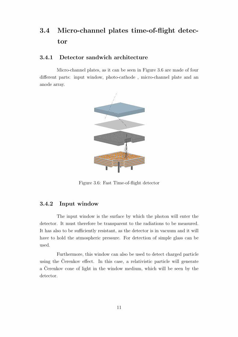
3.4.1 Detector sandwich architecture
Micro-channel plates, as it can be seen in Figure 3.6 are made of four
different parts: input window, photo-cathode , micro-channel plate and an
anode array.
Figure 3.6: Fast Time-of-flight detector
3.4.2 Input window
The input window is the surface by which the photon will enter the
detector. It must therefore be transparent to the radiations to be measured.
It has also to be sufficiently resistant, as the detector is in vacuum and it will
have to hold the atmospheric pressure. For detection of simple glass can be
used.
Furthermore, this window can also be used to detect charged particle
using the Cerenkov effect. In this case, a relativistic particle will generate
a Cerenkov cone of light in the window medium, which will be seen by the
detector.
11

3.4.3 Photo-cathode
Photoelectric effect
When a negatively charged metallic surface is exposed to electromag-
netic radiation above a certain threshold wavelength (typically visible light),
the light is absorbed and electrons are emitted. The emitted electrons can be
referred to as photoelectrons in this context [5]. Although a plain metallic cath-
ode will exhibit photoelectric properties, a custom coating greatly increases the
efficiency. A photocathode usually consists of alkali metals with very low work
functions.
Unfortunately, as it can be seen in Figure 3.7(b), the quantum effi-
ciency of this conversion is not 100% and varies with the material used. Which
means that only a fraction of the incident photons will be converted to elec-
trons and therefore observed. For a good detector, this quantum efficiency
must the highest possible in the spectrum range.
(a) Photo-electric effect (b) Quantum efficiency
Figure 3.7: (a) Photo-electron production (b) Typical quantum efficiency inour design
Advanced photo-cathodes
In order to improve the quantum efficiency of the photo-cathode, some
complex structure can be used (Fig 3.8) [6].
12
(a) Pillar principle (b) Nano-pillar growing [7]
Figure 3.8: (a) Pillar photo-cathode principle (b) Nanoscale realization
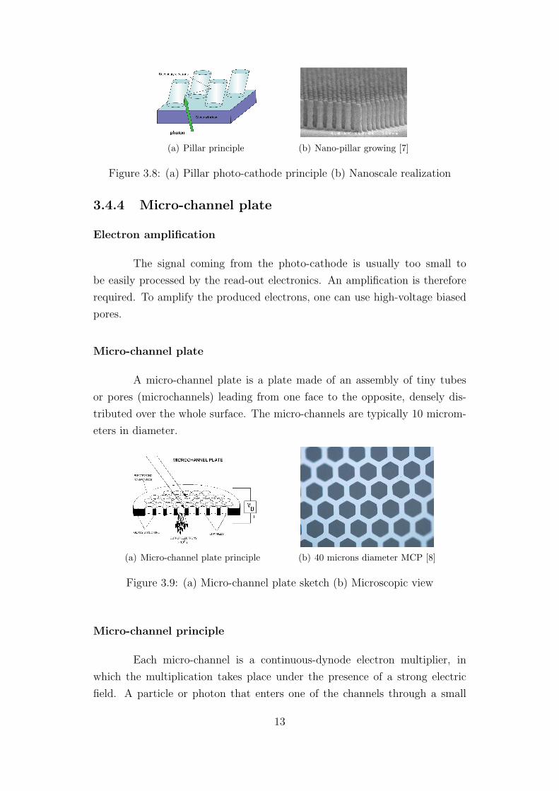
3.4.4 Micro-channel plate
Electron amplification
The signal coming from the photo-cathode is usually too small to
be easily processed by the read-out electronics. An amplification is therefore
required. To amplify the produced electrons, one can use high-voltage biased
pores.
Micro-channel plate
A micro-channel plate is a plate made of an assembly of tiny tubes
or pores (microchannels) leading from one face to the opposite, densely dis-
tributed over the whole surface. The micro-channels are typically 10 microm-
eters in diameter.
(a) Micro-channel plate principle (b) 40 microns diameter MCP [8]
Figure 3.9: (a) Micro-channel plate sketch (b) Microscopic view
Micro-channel principle
Each micro-channel is a continuous-dynode electron multiplier, in
which the multiplication takes place under the presence of a strong electric
field. A particle or photon that enters one of the channels through a small
13

Figure 3.10: Electron amplification in micro-channel plates
orifice is guaranteed to hit the wall of the channel due to the channel being
at an angle to the plate and thus the angle of impact. The impact starts a
cascade of electrons that propagates through the channel, which amplifies the
original signal by several orders of magnitude depending on the electric field
strength and the geometry of the micro-channel plate (Fig 3.10) [9].
3.4.5 Anode plate
At the end of the micro-channel plate, the electrical signal is collected
on an anode array (Fig 3.4). The dimensions of the array give the space
resolution. The more pixels on the anode, the more precisely the location of
an event on the detector is determined.
But, with this structure, they are as many output channels as the
number of anode pads. That is to say that if there are n by n pads, there will
be n2 channels for the front-end electronics.
A way to reduce this number is to use delay lines (Fig 3.11): pads are
connected row by row to a delay line. Whenever a pad receive a pulse coming
from the MCP, it will be transmitted to the delay line and propagate to both
ends of it. The signal is then collected and digitized at each end [10].
This design reduces by a factor n the number of output channels.
Furthermore, the interpolated location of a pulse strike on the line can be
more accurate than the size of the pads (this cannot be achieved with the
array structure only).
14
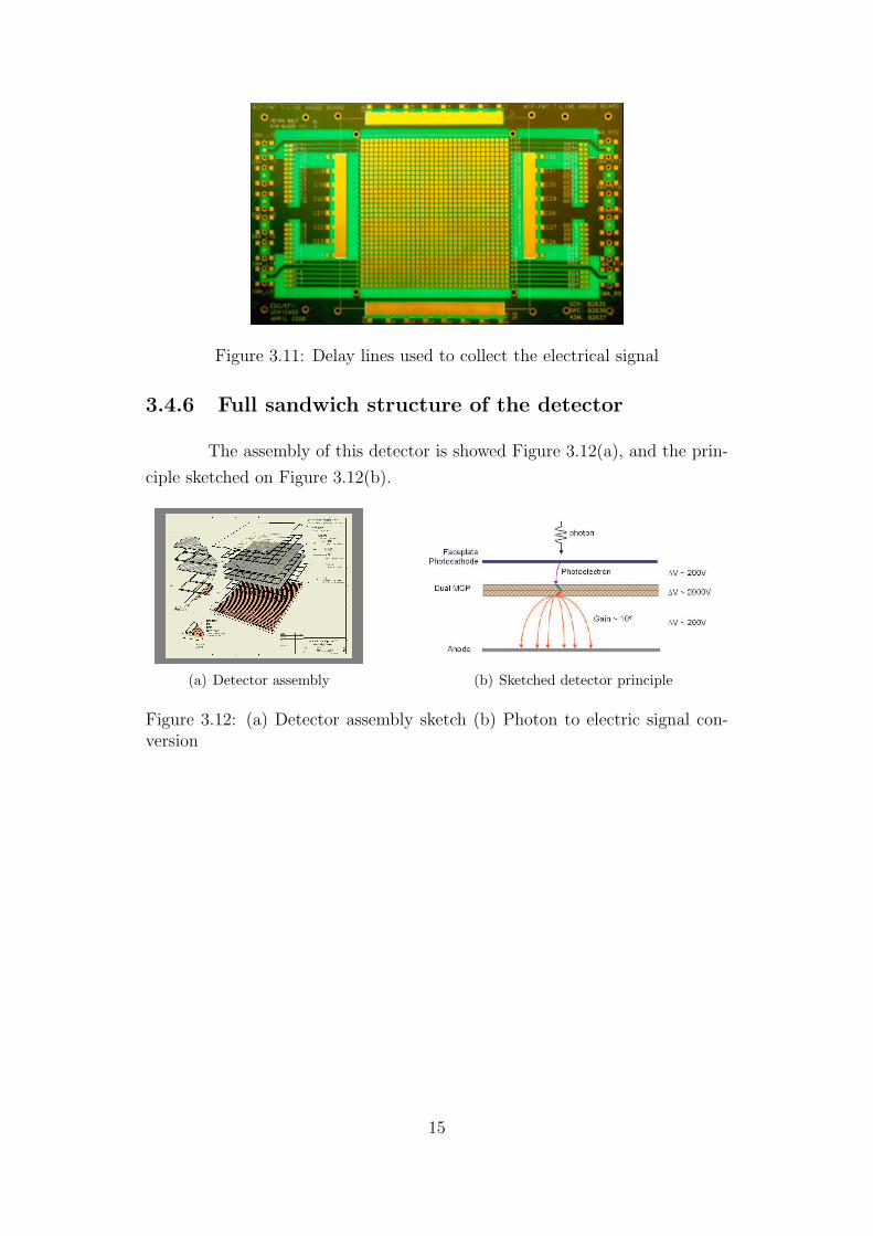
Figure 3.11: Delay lines used to collect the electrical signal
3.4.6 Full sandwich structure of the detector
The assembly of this detector is showed Figure 3.12(a), and the prin-
ciple sketched on Figure 3.12(b).
(a) Detector assembly (b) Sketched detector principle
Figure 3.12: (a) Detector assembly sketch (b) Photon to electric signal con-version
15
4 Signal processing for
Pico-second resolution
4.1 Timing techniques
Present photo-detectors such as micro-channel plate photo-multipliers
(MCP-PMTs) and silicon photo-multipliers achieve rise-times well below one
nano-second. An ideal timing readout electronics would extract the time-of-
arrival of the first charge collected, adding nothing to the intrinsic detector
resolution. Traditionally the best ultimate performance in terms of timing
resolution has been obtained using constant fraction discriminators (CFDs)
followed by high precision time digitization. However, these discriminators
make use of wide-band delay lines that cannot be integrated easily into sili-
con integrated circuits, and so large front-end readout systems using CFD’s
to achieve sub-nsec resolution have are not yet been implemented. Several
other well-known techniques in addition to constant-fraction discrimination
have long been used for timing extraction of the time-of-arrival of a pulse [11]:
• Single threshold on the leading edge.
• Multiple thresholds on the leading edge, followed by a fit to the edge
shape.
• Pulse waveform sampling, digitization and pulse reconstruction.
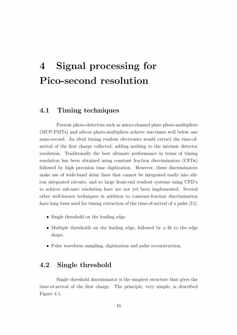
4.2 Single threshold
Single threshold discriminator is the simplest structure that gives the
time-of-arrival of the first charge. The principle, very simple, is described
Figure 4.1.
16
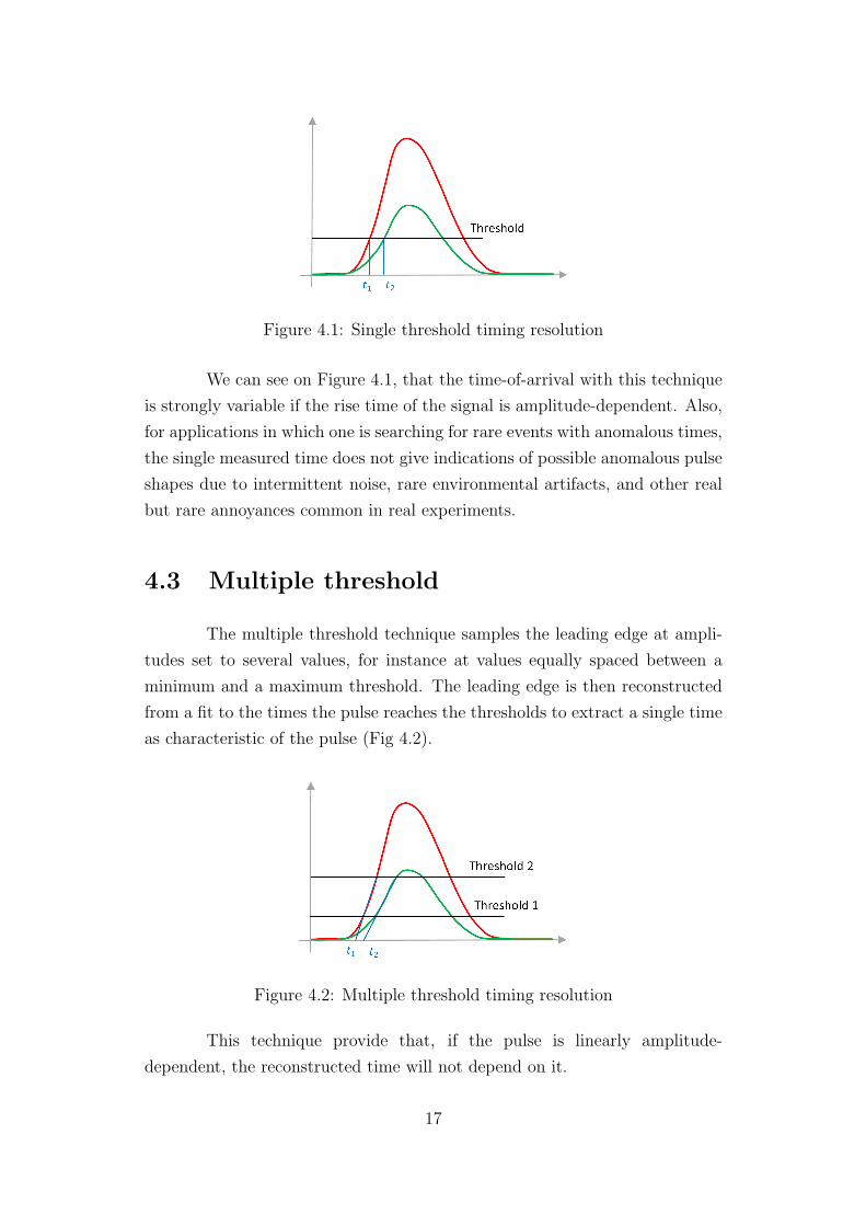
Figure 4.1: Single threshold timing resolution
We can see on Figure 4.1, that the time-of-arrival with this technique
is strongly variable if the rise time of the signal is amplitude-dependent. Also,
for applications in which one is searching for rare events with anomalous times,
the single measured time does not give indications of possible anomalous pulse
shapes due to intermittent noise, rare environmental artifacts, and other real
but rare annoyances common in real experiments.
4.3 Multiple threshold
The multiple threshold technique samples the leading edge at ampli-
tudes set to several values, for instance at values equally spaced between a
minimum and a maximum threshold. The leading edge is then reconstructed
from a fit to the times the pulse reaches the thresholds to extract a single time
as characteristic of the pulse (Fig 4.2).
Figure 4.2: Multiple threshold timing resolution
This technique provide that, if the pulse is linearly amplitude-
dependent, the reconstructed time will not depend on it.
17
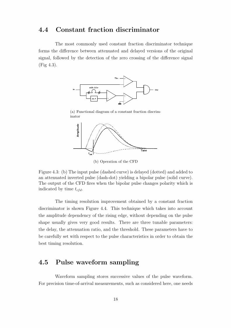
4.4 Constant fraction discriminator
The most commonly used constant fraction discriminator technique
forms the difference between attenuated and delayed versions of the original
signal, followed by the detection of the zero crossing of the difference signal
(Fig 4.3).
(a) Functional diagram of a constant fraction discrim-inator
(b) Operation of the CFD
Figure 4.3: (b) The input pulse (dashed curve) is delayed (dotted) and added toan attenuated inverted pulse (dash-dot) yielding a bipolar pulse (solid curve).The output of the CFD fires when the bipolar pulse changes polarity which isindicated by time tcfd.
The timing resolution improvement obtained by a constant fraction
discriminator is shown Figure 4.4. This technique which takes into account
the amplitude dependency of the rising edge, without depending on the pulse
shape usually gives very good results. There are three tunable parameters:
the delay, the attenuation ratio, and the threshold. These parameters have to
be carefully set with respect to the pulse characteristics in order to obtain the
best timing resolution.
4.5 Pulse waveform sampling
Waveform sampling stores successive values of the pulse waveform.
For precision time-of-arrival measurements, such as considered here, one needs
18

Figure 4.4: Constant fraction timing
to fully sample at least the leading edge over the peak. In order to fulfill the
Shannon-Nyquist condition, the sampling period has to be chosen short enough
to take into account all frequency components containing timing information,
which is that the minimum sampling frequency is set at least at twice the
highest frequency in the signal’s Fourier spectrum.
After digitization, using the knowledge of the average waveform, pulse
reconstruction allows reconstructing the edge or the full pulse with good fi-
delity. The sampling method is unique among the four methods in providing
the pulse amplitude, the integrated charge, and figures of merit on the pulse-
shape and baseline, important for detecting pile-up or spurious pulses.
4.6 Simulation results of comparison between
the four techniques
The four timing techniques presented below have been simulated using
Matlab [12]. At the input, the signal used is a typical MCP output signal. To
this signal is superimposed white shot noise from the MCP and white thermal
noise coming from the electronics (Fig 4.5). For all the techniques, the input
bandwith is taken to be 1.5 GHz. For the pulse sampling technique, a sampling
rate of 20 GSa/s is used.
The time-of-arrival is determined, for all the timing techniques de-
scribed before and plotted versus the number of photo-electrons (strength of
the signal) Figure 4.6. We can clearly see that the sampling technique is the
one providing the best timing resolution out out the four other.
This simulation also shows that the Pico-second precision range is
achievable with MCP’s signals. Coming from this statement a very fast sam-
19

Figure 4.5: Fourier spectra of the noisy signal used in simulation. [11]
pling chip has been designed in order to achieve this Pico-second timing pre-
cision.
Figure 4.6: Time resolution versus the number of primary photo-electrons.[11]
20

5 Detector to Chip integration
5.1 Strip lines
As we discuss previously the bottom of the detector are strip lines that
are running underneath it, as it can be seen on Figure 5.1. These strips lines
are matched to be 50 Ohms. From the output of these lines to the input of
the chip, the distortion of the signal must be as small as possible. Futhermore,
at the input of the chip, the input structure is coplanar. Putting everything
together, we end up with the following specifications:
• 50 Ohms matching.
• Microstrip to coplanar transition.
• Minimizing attenuation of the signal.
• Simple assembly design.
Figure 5.1: Strip line design
21

5.1.1 Strip line models and impedance
Microstrips lines consists of a conducting strip separated from a
ground plane by a dielectric layer (Fig 5.2).
Figure 5.2: Microstrip line principle
Impedance
The impedance of a single strip line is given by the formula [13]:
Z0m =377
2π (εr + 1) /21/2
[ln
(8h
W
)+
1
8
(W
2h
)2
− 1
2
εr − 1
εr + 1
lnπ
2+
1
εrln
4
π
]If we choose one type of substrate (here glass) with a specified thick-
ness, the only remaining parameter is the width W of the lines. In our case,
a width of 3.75mm has been calculated with a high h of 2mm. The glass used
is Borosilicate, with an εr of 4.
Lines losses
There is four different sources for the losses:
• Losses due to the resistance of the line
• Losses due to the dielectric conductivity
• Losses due to the dipole rotation tan(δ)
• The radiative losses
The more important factors appears to be the losses due to the resis-
tance of the line and the losses due to dipole rotation.
Bandwidth
The bandwidth depends mainly upon the dielectric constant and of
the geometry of the strip line, as it can be seen on the following formula [14]:
22
BWTL =3dB
2.3× tan(δ)×√εr× 1
d=
1.3
tan(δ)×√εr× 1
d
5.2 Chip
At the input of the chip, all the inputs (Signals and GND’s) are at
the same metal level. A microstrip line at the input is therefore impossible. A
coplanar line will therefore be used at the input of the chip.
Also, the chip can not simply sit on the glass because of the high
number of I/O pads (144). Chips are usually connected using PCB (Printed
Circuit Board). These boards have different physical and electrical character-
istics (h, εr and metalizations layers), the connection between the glass and
the PCB is therefore not straightforward as we want to avoid 50 Ohms breaks
throughout the line.
On the PCB, one will also eventually go from microstrip to coplanar
lines. The easiest way to do it as presented on Figure 5.3, but it has to be
tested previously.
Figure 5.3: Detector & chip assembly
23

6 Chip structure and
characteristics
In order to get the smallest spread in time-of-arrival of the photon
at the photocathode, we have, according to the previous study, to acquire
the signal coming out the microstrip lines with a rate as high as 40Gs/s, and
keeping an analog bandwidth at the input higher than 2GHz. For that we have
designed a new integrated sampling circuit using a 130nm CMOS process, that
we will present now.
6.1 Fast read-out electronics
As we have seen previously, the required range for the signal acquisi-
tion should be higher that 10Gs/s. At this rate, a straight digitization is for
now impossible. Therefore, simply having an ADC at the input of the line not
doable. The solution is to sample the analog signal at a very high frequency
and then digitize it at a slower rate using ADC’s. This is achieved using the
following structure.
6.2 Structure
6.2.1 General architecture and mechanism
Top design
In order to store the analog value of the signal the structure used is
a switched capacitor array. The circuit principle is very simple and mainly
consist of four different structures presented on Figure 6.1
24
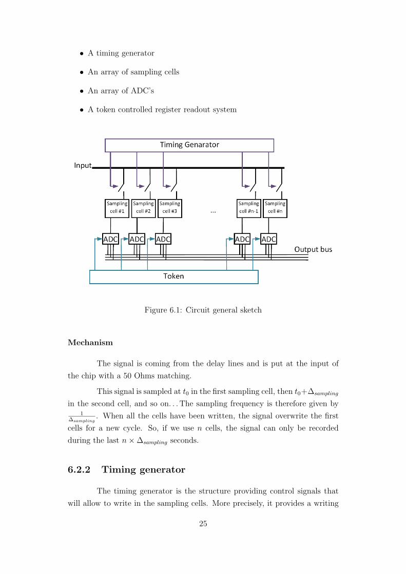
• A timing generator
• An array of sampling cells
• An array of ADC’s
• A token controlled register readout system
Figure 6.1: Circuit general sketch
Mechanism
The signal is coming from the delay lines and is put at the input of
the chip with a 50 Ohms matching.
This signal is sampled at t0 in the first sampling cell, then t0+∆sampling
in the second cell, and so on. . . The sampling frequency is therefore given by1
∆sampling. When all the cells have been written, the signal overwrite the first
cells for a new cycle. So, if we use n cells, the signal can only be recorded
during the last n×∆sampling seconds.
6.2.2 Timing generator
The timing generator is the structure providing control signals that
will allow to write in the sampling cells. More precisely, it provides a writing
25

window to every storage cell. During this window, the input switch of the
storage cell is closed and the signal stored in it.
Figure 6.2: Timing generator principle
The timing generator, as it can be seen on Figure 6.2, is essentially
made of a chain of delay cells. The sampling window is sent at the input of
the timing generator and transmitted trough every delay cells. Each delay
cell takes ∆delay to pass it to the following one. If we have n delay cells in
the timing generator, we have then at the output n sampling window, each of
which is delay by ∆delay compared to the next one.
The sampling frequency achieved by this way is therefore fsampl =1
∆delay. So the smaller is the delay, the higher is the sampling frequency, and
in our case, the better the timing resolution.
6.2.3 Sampling cells
The sampling cell is the structure where the signal is stored. The
sampling cells, being controlled by the timing generator are storing, one after
another the input signal, as it can be seen on Figure 6.3.
Once the control signal has closed the switch at the input of one cell,
this one is going to reach the input signal value as long as the time window
given by the timing generator allows and holds it. The time constant of this
process determines the bandwidth of the sampling cell.
The storage cell must have a very high bandwidth at the input, in
order to be able to follow the rising edges of the fast incoming pulses. Once
the signal is stored it should remains as stable as possible until it has been
digitized by the ADC. Indeed, leakages are responsible for droops before the
ADC has digitized the cell voltage.
26

Figure 6.3: Basic sampling principle
The sampling cell will be described in more details in the following
parts of this report.
6.2.4 ADC’s
The ADC’s we choose to use in our design are ramp ADC’s. This
structure has been choose because of its very good parallelism integration.
And with our design of one ADC per storage cell, this structure is therefore
the more suitable.
The ADC’s are working with the following principle (described on Fig
6.5). A sketch of one ADC can be seen on Figure 6.4.
Figure 6.4: Sketch of the ramp ADC
At the beginning of the digitization process, the sampled value is
available at the output of the sampling cell. When the digitization process
is started, a voltage ramp and the sampling cell stored value are put at the
input of a comparator. In the meantime, the counter starts counting. When
the ramp value reach the sampling cell value, the comparator fires and stops
the counter.
27

Figure 6.5: Ramp ADC principle
The digital value available at the output of the counter is the digitized
value of the sampling cell.
6.2.5 Token controlled register readout system
There is only one output bus to read the data at the output of the
chip. As it can be seen on Figure 6.1, all the ADC’s are connected to this
bus. To avoid conflict during the readout phase, the output of the ADC’s are
serially put on the output bus using a token passing circuit. The role of token
controlled register readout system is therefore to put successively the output
of the ADC’s on the bus one at a time.
6.3 Specification
Coming from the simulation and the structure, the following specifi-
cation have been set for the sampling chip:
28

Chip characteristics
Sampling rate 10GS/s
Analog Bandwidth 2GHz
Dynamic range 0.7V
Sampling window adjustable 500ps-2ns
Sampling jitter 10ps
Maximum latency TBD
Crosstalk 1%
DC Input impedance 50Ω internal
Conversion clock Adjustable 1-2 GHz internal ring oscillator.
Minimum conversion time 2us.
Read clock 40 MHz. Readout time (4-channel)
4× 256× 25ns = 25.6µs
Power 40mW/channel
Power supply 1.2V
Process IBM 8RF-DM (130nm CMOS)
29

7 Operation of the chip
The purpose of this chip is to record very fast pulses from the MCP
detector. The operation is very simple and it has mainly two states. The first
one is called the write state, in which the chip is recording the signals coming
at the input as described. The second one is call the read state and is when
the user is reading the data stored inside the chip.
7.1 Writing
7.1.1 Sampling cell writing
The writing phase is started by launching the timing generator. When
started, this one will controlled the successive closing of the input switches of
every storage cell of one channel. As we previously described, the input signal
is stored, at t0, in the first cell, t0 + ∆sampling, in the second one and so on,
until the last one. Once the last cell has been written, the signal overwrite the
first cell for a new cycle.
As we also said previously, the storage cells record the last n×∆sampling
seconds only. Basically, the cells are then constantly overwritten until a trigger
event.
7.1.2 Trigger event
When an event occurs at the detector (pulse for example), a trigger
bit is raised. The effect of the trigger signal is the following: when at 0, the
signal is let to be written is each cell successively at it has been described.
When the trigger raise to 1, it overrides all the timing control signal and open
all of the storage cells’ input switches.
30

At this time we have then the shape of the signal during the last
n×∆sampling seconds stored in the cells.
The trigger signal also start the digitization process for each cell. At
the end, we then have the digitized value of the signal during the last n ×∆sampling seconds before the trigger available.
7.2 Reading
The reading phase starts after a trigger event, when the signal has
been digitized and its values are available from the chip. During the reading
phase, the token controlled readout register serially assert every stored value
on the output bus. These values are then read externally, using a FPGA for
example.
31

8 Storage cells
8.1 Storage cell principle
Figure 8.1: Elementary sampling cell
The most simplest sampling cell, is only a capacitor, in which the
input voltage will be stored . There are three steps to store the data :
Write state
The first one is the write state, when the write switch is closed and
read switch open (Fig 8.2). During this state, the capacitance is being charged
by the input voltage Vin.
Figure 8.2: Write state
32

Intermediate state
During this state, both read and write switches are open (Fig 8.3),
the value stored should not evolve. We will see later that it is usually not the
case due to leakages.
Figure 8.3: Intermediate state
Read state
The third one is the read state, when the write switch is open and the
read switch is close (Fig 8.4). The output voltage is then given by the voltage
stored by the capacitance during the write state.
Figure 8.4: Read state
This is the structure always employed to sample an analog signal. The
principle is simple, but they are several issues that must be taken care of when
designing. The main ones are:
• Write state bandwidth
• Charge leakage
• Charge injection
8.1.1 Write state bandwidth
Basically, the write state consist of charging the input capacitance.
When closed the write switch resistance is not zero and can be relatively high
33
(typically around 10kΩ ). Therefore, one must take care of the cutoff frequency
of this RC circuit.
8.1.2 Charge leakage
Between the read and write state, when both read and write switch are
open, the charge stored on the input capacitance may evolve due to several
effect. This effect will lead to reading an output that could be perceptibly
different of the input. The predominant contributions of such a leakage are
the following :
Capacitor leakage
When charged, the insulating layer between the two plates of the tran-
sistor, theoretically prevent the charge going from one plate to the other. Prac-
tically, there is always a leakage current between the two plates discharging
slowly the capacitor. This leakage is small in our case.
Switch leakage
When off, the equivalent resistance of the switch is ideally infinite, in
reality this resistance has a high value, but not infinite. Therefore, there is a
leakage current trough the off switch too.
8.1.3 Charge injection
The charge injection is the small charge transferred to the storage
capacitor via the interelectrode capacitance of the switch and the stray capac-
itance when switching to the hold mode. The offset step is directly proportional
to this charge:
Offset error = Incremental Charge/Capacitance = ∆QC
It can be reduced somewhat by lightly coupling an appropriate polarity
version of the hold signal to the capacitor for a first-order cancellation. The
error can also be reduced by increasing the capacitance, but this increases
acquisition time and decreases the bandwidth. The charge injection is also
amplitude dependent, which makes a total cancellation hard to realize.
34

8.1.4 Output current level
In the architecture shown Figure 8.1, one can see that we use on the
output the same charge as it has been stored at the input. This is not the
smartest design as we will be confronted to all the previous factors of error
when moving this charge to the output. Therefore, we have to think about
an architecture that prevents the charge to flow again during the read phase,
responsible for voltage droops.
35

8.2 Input switch
The input switch is the first stage of our circuit and must therefore
be carefully studied in order to preserve the signal transfer to the storage
capacitor.
8.2.1 Design
The design of the switch is shown on Figure 8.5.
Figure 8.5: Switch design
8.2.2 Large signal analysis
The switch consist of the association of two FET’s: one Nfet and one
Pfet in parallel controlled by the “en” tension. Indeed, two FET’s are necessary
is one wants to switch in the full range given by the power supplies. The two
important parameters are the RON and ROFF resistances of the switch:
Switch RON
As the switch consist in the association of one Pfet and one Nfet in
parallel, the RON will be given by the RON resistance of each fet.
In the ON state of the switch, the voltage across the switch should
be small and vGS should be large. Therefore, the fet is assumed to be in the
nonsaturation region. And we have:
iD =KW
L
[(vGS − VT ) vDS −
v2DS
2
]
The rON resistance of the switch is then given by:
36

rON =1
∂iD/∂vDS=
L
KW (VGS − VT − VT )
This resistance is plotted Figure 8.6(a) for both Pfet (red) and Nfet
(blue). The resistance become almost infinite for VGS < VT for both transistors.
(a) Resistance of Pfet and Nfet (b) Resistance of the switch obtained bya Spice simulation
The switch resistance is the parallel addition of the resistances of the
Pfet and the Nfet, it has been simulated with Spice, and is plotted Figure
8.6(b).
On the Figure 8.6, is plotted the experimental resistance obtained with
Spice and the equivalent resistance obtained with Matlab. We can see that
the experimental curve fits very well the model of the resistance of a Pfet and
an Nfet in parallel.
Figure 8.6: Resistance of the switch given by Spice & Matlab
37
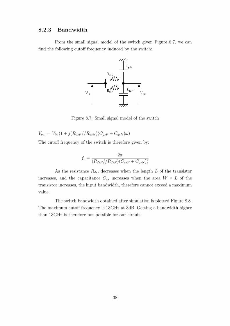
8.2.3 Bandwidth
From the small signal model of the switch given Figure 8.7, we can
find the following cutoff frequency induced by the switch:
Figure 8.7: Small signal model of the switch
Vout = Vin (1 + j(RdsP//RdsN)(CgsP + CgsN)ω)
The cutoff frequency of the switch is therefore given by:
fc =2π
(RdsP//RdsN)(CgsP + CgsN))
As the resistance Rds, decreases when the length L of the transistor
increases, and the capacitance Cgs increases when the area W × L of the
transistor increases, the input bandwidth, therefore cannot exceed a maximum
value.
The switch bandwidth obtained after simulation is plotted Figure 8.8.
The maximum cutoff frequency is 13GHz at 3dB. Getting a bandwidth higher
than 13GHz is therefore not possible for our circuit.
38

Figure 8.8: Simulated switch bandwidth
39

8.3 Non-linear storage cell
The first designed cell can be seen Figure 8.9. In this structure, a
common source structure is used to read the input capacitance. The advantage
of this structure is its very large current gain, allowing to read the deposited
charge with almost no current flow, and therefore minimum leakages. But the
voltage Vout dependence with Vin is not linear.
Figure 8.9: Electric structure of the non-linear storage cell
8.3.1 Improved structure
Figure 8.10: Storage cell using the gate capacitance
In the structure Figure 8.10, there is no more physical input capaci-
tance. The capacitance used to store the signal is the gate capacitance of the
Nfet. This structure presents two main advantages.
First, the gate capacitance which already exists and was in parallel
with the input capacitance (Fig 8.9) is not seen as a parasitic capacitance
anymore.
Secondly, as this input capacitance is very small, the input bandwidth
will be more larger.
40

8.3.2 Large-signal analysis
Depending of the input voltage, the transistor can be operating in
different regions:
Figure 8.11: Large-signal schematics
Cutoff region
If vGS − VT ≤ 0, then iD = 0
Yet : vGS = vin−VSS That is to say: for vin from VSS to VSS +VT ; vout = VDD.
Saturation region
From the large signal schematics (Fig 8.11) we can derive the following equa-
tions:
iL =µCox
2
W
L(VGS − VT )2
With:
vGS = vin − VSS
And:
vout = VDD −RLiL
So:
vout = VDD −RLµCox
2
W
L(vin − VSS − VT )2
The previous equation justify the non-linear behavior of this cell: the output
depends quadratically on the input. Such a transfer function does not fit very
well with the further digitization. But this structure has the advantage of
being very fast.
41

Triode region
If 0 < vDS ≤ (vGS − VT ) then iL =µCox
2
W
L
[(vGS − VT )− vDS
2
]vDS
2
The transistor will then enter the saturated region when vDS(sat) = vGS−VT .
Yet, from the schematics Fig 8.11:
vDS = vout − VSS
vGS = vin − VSS
vout = VDD −RLiL
So:
vGS − VT = vDS(sat)
⇔ vin(sat)− VSS − VT = vout(sat)− VSS
⇔ vin(sat)− VSS − VT = VDD − VSS −RLµCox
4
W
L(vin(sat)− VSS − VT )2
So, the transistor will enter the triode region when:
⇔ vin(sat)− VSS − VT =4L
RLµCoxW
√1 +(VDD − VSS)RLµCoxW
L− 1
Figure 8.12: Plot of the vin(sat) value versus RL
Figure 8.12 is plotted vin(sat) versus RL. We can see that for a re-
sistance value smaller than 5kΩ, vin(sat) is always higher than the maximum
supply voltage (ie 1.2V). Therefore, for such resistance values, the transistor
will remain in the saturation region.
42
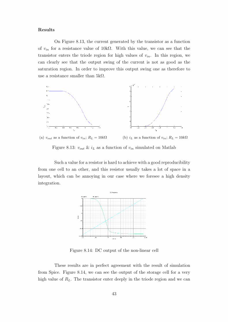
Results
On Figure 8.13, the current generated by the transistor as a function
of vin for a resistance value of 10kΩ. With this value, we can see that the
transistor enters the triode region for high values of vin. In this region, we
can clearly see that the output swing of the current is not as good as the
saturation region. In order to improve this output swing one as therefore to
use a resistance smaller than 5kΩ.
(a) vout as a function of vin; RL = 10kΩ (b) iL as a function of vin; RL = 10kΩ
Figure 8.13: vout & iL as a function of vin simulated on Matlab
Such a value for a resistor is hard to achieve with a good reproducibility
from one cell to an other, and this resistor usually takes a lot of space in a
layout, which can be annoying in our case where we foresee a high density
integration.
Figure 8.14: DC output of the non-linear cell
These results are in perfect agreement with the result of simulation
from Spice. Figure 8.14, we can see the output of the storage cell for a very
high value of RL. The transistor enter deeply in the triode region and we can
43
see (Figure 8.14), that the output swing is then completely flattened for high
value of vin.
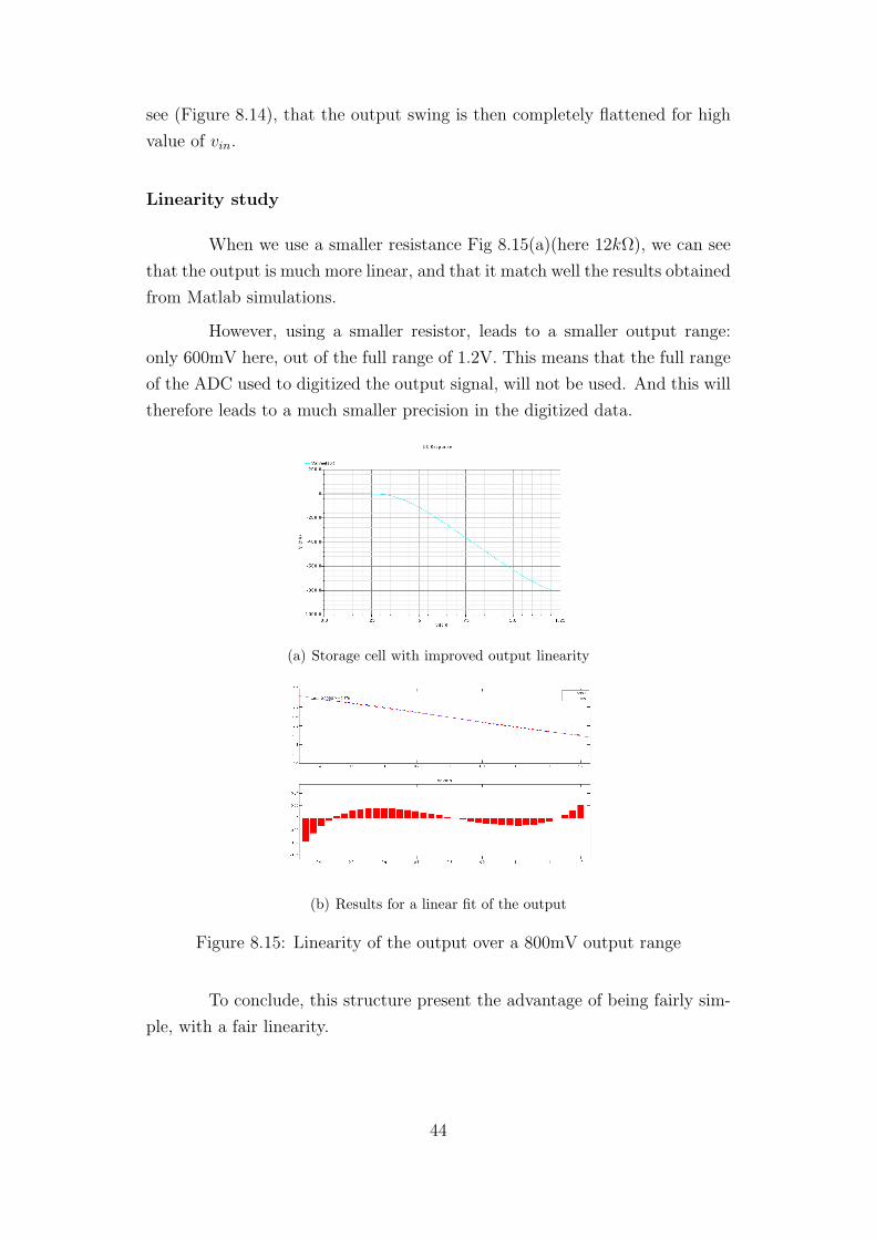
Linearity study
When we use a smaller resistance Fig 8.15(a)(here 12kΩ), we can see
that the output is much more linear, and that it match well the results obtained
from Matlab simulations.
However, using a smaller resistor, leads to a smaller output range:
only 600mV here, out of the full range of 1.2V. This means that the full range
of the ADC used to digitized the output signal, will not be used. And this will
therefore leads to a much smaller precision in the digitized data.
(a) Storage cell with improved output linearity
(b) Results for a linear fit of the output
Figure 8.15: Linearity of the output over a 800mV output range
To conclude, this structure present the advantage of being fairly sim-
ple, with a fair linearity.
44

8.3.3 Small signal analysis
Small signal model of the circuit
Figure 8.16: Small-signal model of the cell
Figure 8.16 is the small-signal model of the cell. With this model we
can determine the transfer function of this cell, and its bandwidth.
Transfer function
In order to simplify this study,we will ignore, on the first order, the
Cgd capacitance. Hence, from the Figure 8.16, we have :
iin = igs
vGS =1
jCGSωigs
vin − vgs = RSiin
So:
vin = vgs (1 + jRSCGSω)
vDS = vout = RDSiDS
vout = RLiL
iL + gmVGS + iDS = 0
voutRL
+ gm
(vin
1 + jRSCGSω+voutRDS
)The transfer function of the cell is then the following:
voutvin
= −(
RLRDS
RL +RDS
)gm
1 + jRSCGSω
45

From it, we can extract the gain of the cell :
G = gm
(RLRDS
RL +RDS
)
Input bandwidth
From the previous study, we can see that the cutoff frequency of the
cell is given by RSCGS. To improve the input bandwidth, one as therefore
to reduce both RS and CGS. To do so, for CGS, the dimensions of the input
capacitor have to be the chosen as small as possible. But one cannot make
them the smallest dimensions of the design, because if so, the capacitance
parameters would be too much scattered.
Figure 8.17: Input bandwidth
Figure 8.17, we can see the input bandwidth of the cell. We can see
that the bandwidth is really high (around 20GHz), witch allow us a very fast
sampling rate. However, this cutoff frequency is higher than the 13GHz cutoff
frequency that we determine before. In this case, the switch will therefore the
component limiting the bandwidth.
8.3.4 Read & Write state of the cell
The read and write sequence is not as simple as one could think.
Indeed, Figure 8.18, one can see that the parasitic capacitances of a transistor
are dependent of the state of the transistor. Therefore, in order to read and
46

write the same input, the transistor has to be in the same state during the
read and the write phase.
Figure 8.18: Voltage dependence of CGS, CGD, and CGB as a function of VGS
In order to have the transistor in the same state during the read and
write phase, the read switch has to be closed during the write state too. The
read & write sequencing is then given by the Figures 8.19
(a) Write state (b) Intermediate state (c) Read state
Figure 8.19: Read & write sequencing
8.3.5 Cell issues
Input bandwidth
Due to the non-infinite input bandwidth, the signal tracked during the
write phase is not the same as the input; there is an attenuation for the higher
frequencies as we can see in Figure 8.20.
47

Figure 8.20: Visualization of the difference between the input signal and the
signal on the sampling cell
Charge leakage
As we discussed previously, there are two sources of charge leakage:
the capacitance and the switch. For the capacitance, the charge leakage is
dependent of the area of the Nfet used. In our process, this charge leakage is
quite important: 0.7pA/µm2.
The time necessary to loose 1mV is given by:
i =∂q
∂t= C
∂U
∂tYet:
i = 11fA
C = 200aF
Then:∂U
∂t= 55V/s
So:
∆t1mV = 18µs
There is also the discharge of the capacitance trough the switch. The time
constant of this discharge is given by τ = ROFFCIN
Let’s calculate the order of magnitude necessary for ROFF to make the leakage
trough the switch negligible compared to the leakage trough the Nfet.
The voltage on the gate is following the exponential law:
V = V0e− tτ
48

Let’s take an input voltage of 600mV, and a time constant to loose 1mV ten
times higher than the previous one: ∆t1mV = 200µs
We have then:
V0 − 1mV = V0e− t1mV
τ
τ =−∆t1mV
ln(V0−1mV
V0
) = 0.12
ROFF =τ
C= 600TΩ
This determined value of ROFF is much more higher than the real
achievable value for the switch. It means therefore that the switch will be the
most leaking component in our design.
Determination by simulation of the most leaking component
In order to find what is the limiting parameter the following simulation
has been done: a circuit with an ideal capacitance (no leakage) of the same
value of the transistor capacitance and the real circuit are been simulated
Figure 8.21
49

(a) Switch with ideal input capacitance
(b) Switch with the standard input transistor
Figure 8.21: Comparison of the sampling with an ideal and non-ideal input
capacitance
The two circuits of the Figures 8.21 have been simulated under the
same conditions: 600mV is set at the input of each cell, then the write switch
is open and the output of the both cells are compared Figure 8.22. What we
basically see in this figure is the decreasing of the voltage stored on the capac-
itor due to the leakage. As the two curves are similar, we can obviously say
that the leakage trough the capacitance is negligible compared to the leakage
of the switch. A special effort has therefore to be made for the design of the
switch in order to reduce this leakage. This means increasing ROFF .
50

Figure 8.22: Comparison of the stored value with an ideal capacitance (red)
and the real circuit (black)
Charge injection
The most constraining parasitic effect in this storage cell during the
write phase is the charge injection of the switch. With no compensation, the
charge injection is presented Figure 8.23. We can see that whereas the value
stored on the input capacitance is the desired one (600mV); when the switch
is closed, a charge (negative) is injected making the input value evolve.
Figure 8.23: Visualisation of the charge injection when closing the write switch
This charge injection can be reduced by an elaborated design of the
switch [15], or could be either taken care of by calibrating each cell.
51

8.3.6 Read state
During the read state the write switch is open and the read switch
closed. The output is available and can be sent to the comparator for the
digitization. During this phase, the output must stay as stable as possible
and as close as possible to the value of the corresponding input. The charge
leakage must be as small as possible and the digitization as fast as possible.
Figure 8.24, is the schematic view of the storage cell simulated with
Spice. The result of the simulation can be seen Figure 8.25. There are three
phases, according to the previous section. On the figure, we can clearly see
the input voltage evolving on the gate of the Nfet for different regimes. But in
good agreement with the previous section the voltage is restored to the initial
value during the read phase.
Figure 8.24: Simulated storage cell
52

Figure 8.25: Evolution of the output during the read and write states
53
8.4 Linear storage cell
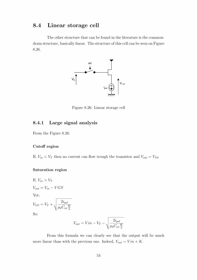
The other structure that can be found in the literature is the common-
drain structure, basically linear. The structure of this cell can be seen on Figure
8.26.
Figure 8.26: Linear storage cell
8.4.1 Large signal analysis
From the Figure 8.26:
Cutoff region
If, Vin < VT then no current can flow trough the transistor and Vout = VSS
Saturation region
If, Vin > VT
Vout = Vin − V GS
Yet:
VGS = VT +
√√√√ 2ipolµ0Cox
WL
So:
Vout = V in− VT −√√√√ 2ipolµ0Cox
WL
From this formula we can clearly see that the output will be much
more linear than with the previous one. Indeed, Vout = V in+K.
54

8.4.2 Linear cell with real current source
Figure 8.27: Linear storage cell with a real current source
In order to implement the current source (Fig 8.26) of the circuit, we
use a Nfet biased by the voltage Vpol (Figure 8.27 ), we have then:
ipol =µ0Cox
2
Wpol
Lpol(VGS − VT )2
So:
Vout = V in− VT − (Vpol − VT )
√W
L
LpolWpol
DC characteristic
Figure 8.28: DC characteristic of the cell
Figure 8.28 the output (black) vs input (blue) of the cell is plotted.
One can see that the linearity of the cell is particularly good. However, having
55

an output using the full range of the DC sources (from GND to VDD), is not
achievable.
Figure 8.29: Linear fit of the output
We can check this linearity on Figure 8.29. The linearity is improved
by a factor 10 compared to the previous cell.
8.4.3 Small signal analysis
Figure 8.30: Small signal model of the cell
From the Figure 8.30 we have:
Vin − Vout = iin
(Rin +
1
jCGSω
)Vout = rDSiDS
Vout = ipol
(rpol +
1
jCeqω
)
56

iin + gmVGS + iDS = ipol
At the first order we can neglect iDS and iin compared to the other current
level.
Yet:
gmVGS = ipol
Vout = gmVGS
(Req +
1
jCeqω
)
VGS =1
jCgsω
Vin − VoutRin + 1
jCgsω
=Vin − Vout
1 + jRinCgsω
So:
Vout = (Vin − Vout)gmReq1
1 + jRinCgsω
1
1 + jReqCeqω
Finally:
VoutVin
=1
1 + (1+jReqCeq)(1+jRinCgs)gmReq
From this equation, we can see that in addition to the expected input
pole (RinCgs),a second pole is added at the output due to the floating source
potential of the Nfet. This pole is given by ReqCeq. Req is in fact the RDS of
the biasing transistor and Ceq is the sum of all the capacitance of the biasing
transistor.
8.4.4 Input & Output bandwidth
Figure 8.31: Input and output bandwidth of the cell
57

On Figure 8.31, we can see the input and output bandwidth of the cell.
We can check that the input bandwidth is as high as the bandwidth obtained
with the previous cell. But the output is slower, due to the second pole.
8.4.5 Read state
Figure 8.32: Evolution of the input and the output during the read state, the
red curve is the input, the black one is the signal stored in the input Nfet, the
yellow and purple curves are the control signals for the switch, and the pink
curve is the signal at the output of the cell.
Figure 8.32, we can see during the read and write states the input (in
black) and the output (in pink). As previously stated, the output is evolving
much slower than the input. Therefore, the source voltage of the Nfet is
evolving during the read state. Yet, in Figure 8.18, we saw that the value of
the input capacitance depends on the working condition of the Nfet. If VS is
evolving it will make VG evolve too.
However, it was found in an improved study of the cell, that this pole
can be rejected high enough to allow a correct reading and writing, as it can
be seen on Figure 8.33
58
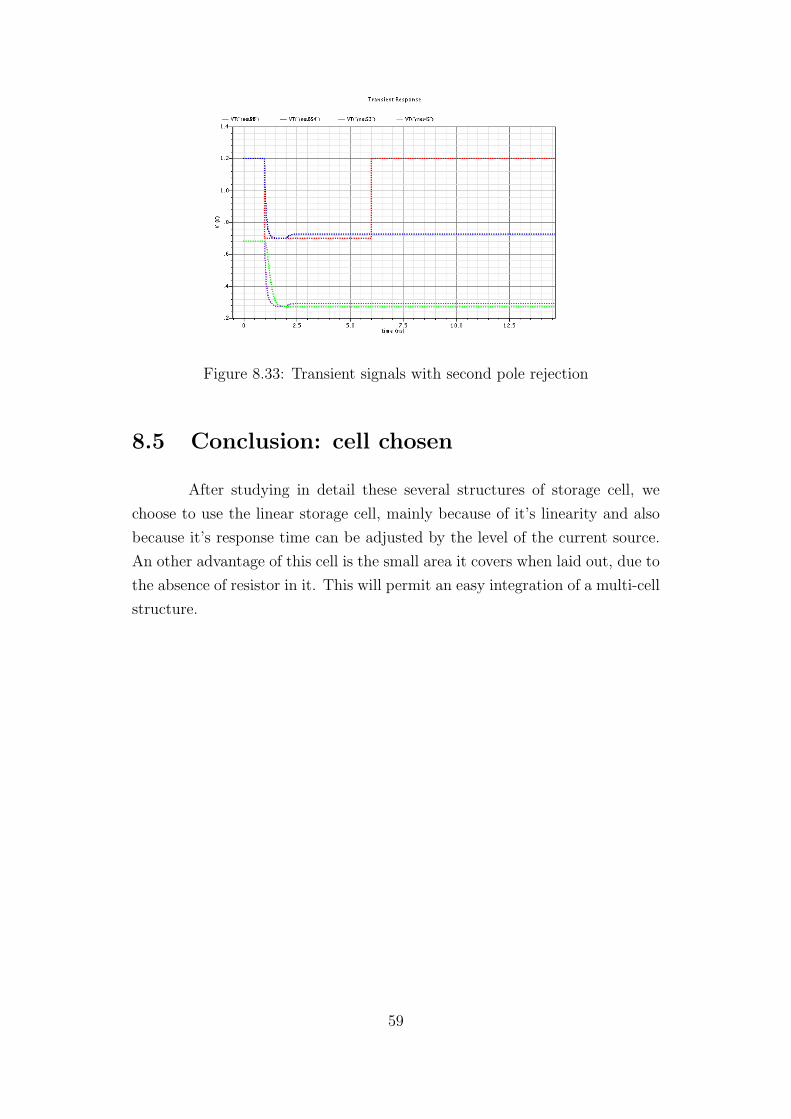
Figure 8.33: Transient signals with second pole rejection
8.5 Conclusion: cell chosen
After studying in detail these several structures of storage cell, we
choose to use the linear storage cell, mainly because of it’s linearity and also
because it’s response time can be adjusted by the level of the current source.
An other advantage of this cell is the small area it covers when laid out, due to
the absence of resistor in it. This will permit an easy integration of a multi-cell
structure.
59

9 Design
Following the previous study a storage cell has been designed for the
sampling chip. It has been done using the kit CMRF 8 SF of IBM under
Cadence.
9.1 Storage cell
9.1.1 Schematic view
The schematic view of the storage cell is shown Figure 9.1
Figure 9.1: Schematic view of the storage cell
The different parts of the cell can be seen on Figure 9.2. The cell
consists of five different parts:
• The input switch
60

• The input capacitance and Nfet
• The current source
• The multiplexor
• The output switch
Figure 9.2: Schematic bloc description
9.1.2 The input switch
The present timing generator, does not have a fully differential output.
Therefore it is not possible to control a PFet, Nfet switch. We therefore only
used a single Pfet switch, allowing a signalrange from 1.2V to .4V at the input.
A better switch with a differential output from the timing generator, would
cover full-range signals at the input, and would also have a smaller value for
the resistance of the switch, and reduce the charge injection. The actual charge
injection can be seen on Figure 8.33. It is not negligible at all, but as it will be
identical for every cells, it can be seen as a parasitic offset that can be canceled
by a calibration of each cell.
In the next chip, this input switch will be improved a lot, mainly
having the timing generator output differential. Therefore, charge injection
cancellation techniques will be used, the input resistance will be reduced lead-
ing to a wider input bandwidth, and the input range will cover the full range
allowed by the tecnology.
61

9.1.3 The input capacitance and Nfet
In this chip we choose to add an additional input capacitor to the
parasitic capacitor of the input Nfet, indeed the value of this one was too small
20fF, and therefore too much subject to leakage, noise, and charge injection.
Furthermore, the characteristic of a real capacitor are much reliable
than a parasitic one, in particular the capacitance does not depend on the bias
voltages at its input (as it is the case for the parasitic transistor of the Nfet)
and are also very defined. Unfortunately, the layout of a physical capacitor
takes a lot more space than a simple transistor, leading to a more complicated
layout and integration.
9.1.4 The current source
The current source is a simple Nfet driven externally, the value of the
current set by the current source controls the time response of the circuit (the
more current, the fastest is the circuit) but also the drop of voltage between
the input and the output. Having this external control of the current source is
mandatory in this first chip in order to tune the cell and get the best results.
9.1.5 The multiplexer
The multiplexer is the structure that controls the input signals to be
switched. Indeed the switch can be either controlled by the timing signal or
the trigger signal when an event has been recorded. This structure is a simple
CMOS multiplexer.
9.1.6 The output switch
We did not detail this switch in the previous section, and yet it plays
a very important role in the chip as we will see now:
Indeed, when simulating this chip without it, we were aware that the
leakages in the cell were very important, and that not taking care of them,
would lead to loose a huge amount of our signals even before starting the
digitization.
We can see that the subthreshold current, which is the leakage current
62
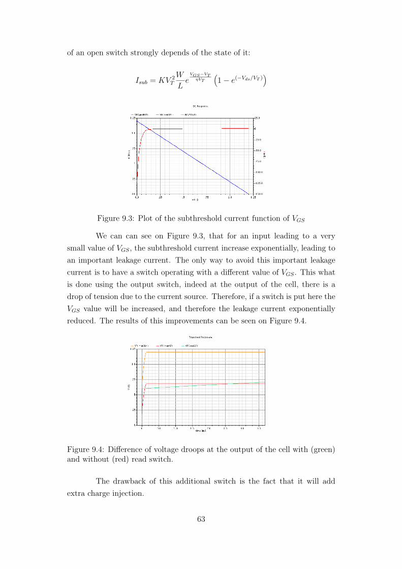
of an open switch strongly depends of the state of it:
Isub = KV 2T
W
LeVGS−VTηVT
(1− e(−Vds/VT )
)
Figure 9.3: Plot of the subthreshold current function of VGS
We can can see on Figure 9.3, that for an input leading to a very
small value of VGS, the subthreshold current increase exponentially, leading to
an important leakage current. The only way to avoid this important leakage
current is to have a switch operating with a different value of VGS. This what
is done using the output switch, indeed at the output of the cell, there is a
drop of tension due to the current source. Therefore, if a switch is put here the
VGS value will be increased, and therefore the leakage current exponentially
reduced. The results of this improvements can be seen on Figure 9.4.
Figure 9.4: Difference of voltage droops at the output of the cell with (green)and without (red) read switch.
The drawback of this additional switch is the fact that it will add
extra charge injection.
63

9.1.7 Layout
The layout of this cell can be seen on Figure 9.5.
Starting from the bottom of the figure, we can first see the storage
capacitance, taking most of the space. This capacitor is an inter-digited ca-
pacitor, in order to avoid cross-talk from the adjacent capacitor, it has been
shielded by a top metal plate and the side wall.
Then we can see on the left the input Nfet, which has been designed
close to the current source to obtain a better matching.
On the right, we have first the multiplexer that will select between the
timing control signal and the trigger. And then the input switch.
Going towards the top of the cell, we can then see the structure of
the input line for the signal. This structure will be discussed along with the
integration of the cells to make a channel.
On the very top of the cell, one can see a series of three double invert-
ers. These inverters are in fact reshapers for the fast control signals: timing
control, trigger, and output switch control.
64
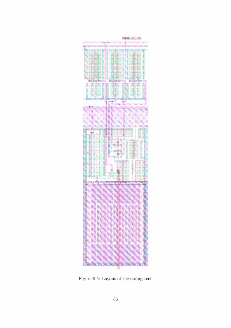
Figure 9.5: Layout of the storage cell
65
9.2 Storage cell assembly
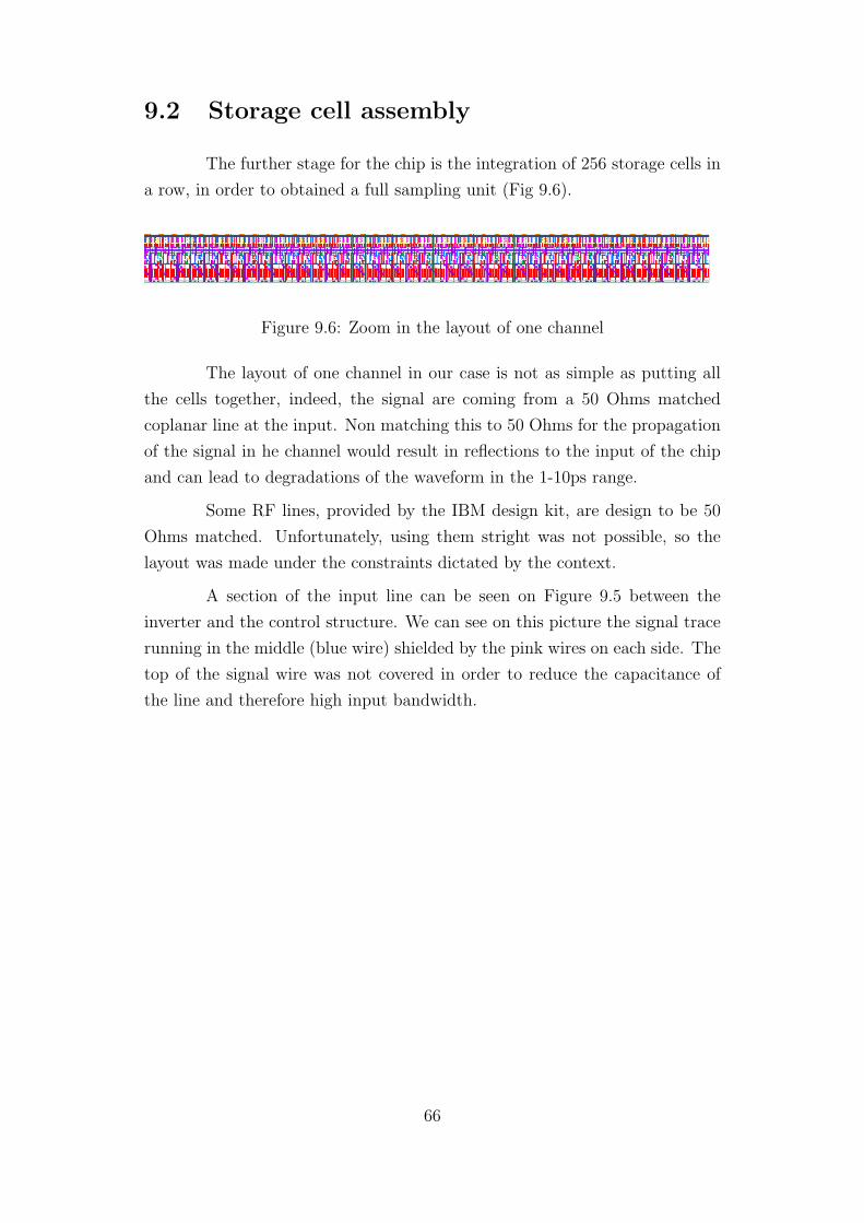
The further stage for the chip is the integration of 256 storage cells in
a row, in order to obtained a full sampling unit (Fig 9.6).
Figure 9.6: Zoom in the layout of one channel
The layout of one channel in our case is not as simple as putting all
the cells together, indeed, the signal are coming from a 50 Ohms matched
coplanar line at the input. Non matching this to 50 Ohms for the propagation
of the signal in he channel would result in reflections to the input of the chip
and can lead to degradations of the waveform in the 1-10ps range.
Some RF lines, provided by the IBM design kit, are design to be 50
Ohms matched. Unfortunately, using them stright was not possible, so the
layout was made under the constraints dictated by the context.
A section of the input line can be seen on Figure 9.5 between the
inverter and the control structure. We can see on this picture the signal trace
running in the middle (blue wire) shielded by the pink wires on each side. The
top of the signal wire was not covered in order to reduce the capacitance of
the line and therefore high input bandwidth.
66
9.3 Channel
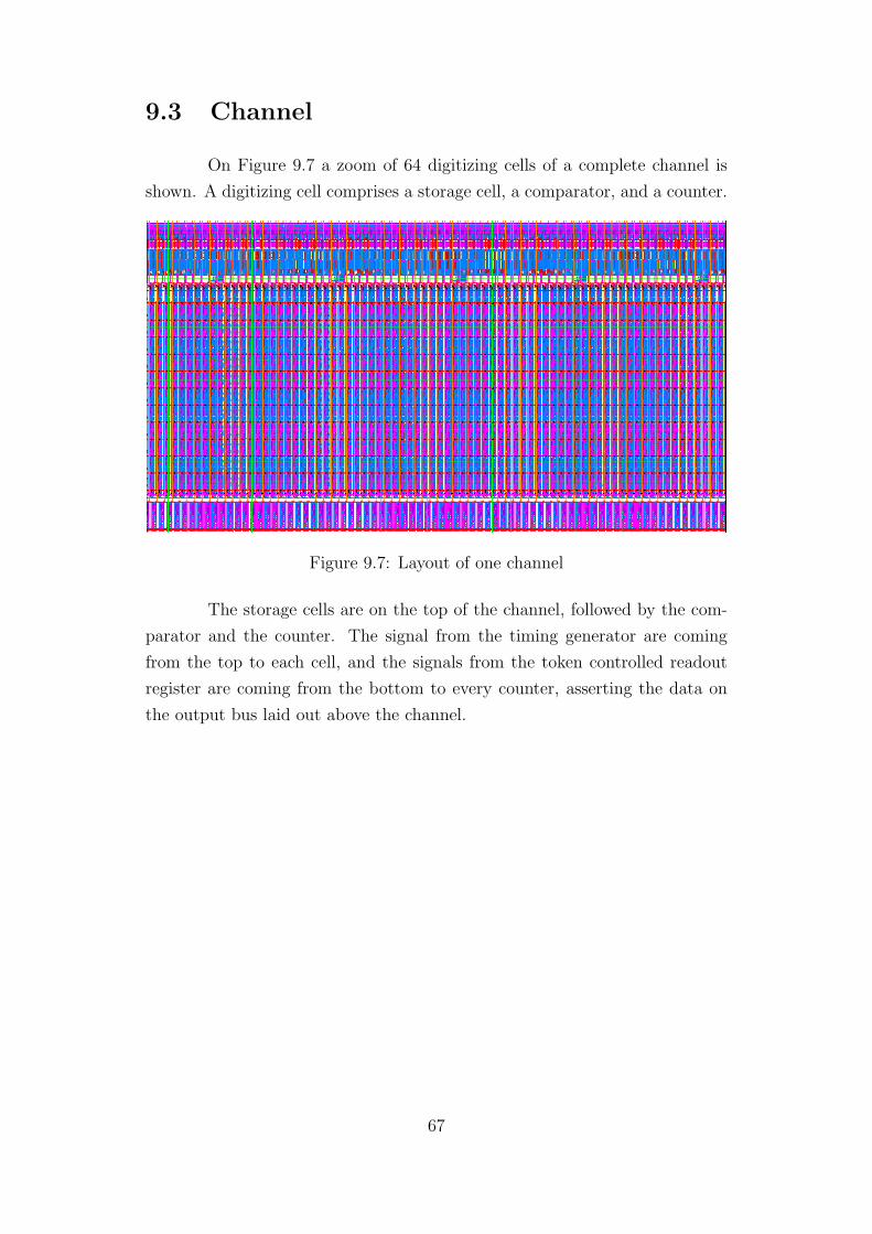
On Figure 9.7 a zoom of 64 digitizing cells of a complete channel is
shown. A digitizing cell comprises a storage cell, a comparator, and a counter.
Figure 9.7: Layout of one channel
The storage cells are on the top of the channel, followed by the com-
parator and the counter. The signal from the timing generator are coming
from the top to each cell, and the signals from the token controlled readout
register are coming from the bottom to every counter, asserting the data on
the output bus laid out above the channel.
67

9.4 Chip
The layout of the entire chip can be seen on Figure 9.8.
Figure 9.8: Final layout of the chip submitted
On this Figure, we can clearly see the four input channels on the top
left. There is a fifth channel that will be used to monitor the signal coming
from the timing generator.
At the bottom of the chip some test structures have been placed: a
sampling cell, a comparator, a ring oscillator and a counter.
All the structures are tied to the 144 pads of the chip (in red). The
connectivity of each pad is shown Figure 9.9.
This chip has been successfully submitted to MOSIS, an academic
facility which provides access to fabrication of prototype and low-volume pro-
68

Figure 9.9: Chip pinou
duction quantities of integrated circuits at low cost.
69

10 Conclusion
During this internship, a new very fast high bandwidth chip has been
designed for pico-second time-of-fight applications, using a very small technol-
ogy (130nm IBM). The internship started by an in-depth study of the pico-
second project and the sampling cells present in the literature. Then the
sampling process has been studied, simulated, designed and laid out using the
Cadence software tool. The cells have being integrated in a channel allowing
a full digitization of incoming signals. The internship ended by designing the
full chip, and successfully submit it to the MOSIS academic after verification
and stream out. This internship was a wonderful experience, it allowed me
to acquire a unique experience in CMOS VLSI design, and therefore complete
adequately my student formation. Doing this internship in the United States,
in particular at the University of Chicago, i got an incredible experience in
both technique and linguistic, therefore I would like to thank my professors
H. J. Frisch and J. F. Genat, for choosing me and giving me this opportunity,
and also for all the support and the attention they provided me.
70

Bibliography
[1] Henry Frisch et al. The Development of Large-Area Fast Photo-detectors. http://psec.uchicago.edu/other/Project_description_
nobudgets.pdf, 2009.
[2] W. S. C. Williams. Nuclear and Particle Physics. Oxford University Press,1991.
[3] H. Bruining Physics and applications of secondary electron emissionMcGraw-Hill Book Co., Inc.; 1954.
[4] H. E. Iams and B. Salzberg. The secondary emission phototube Proc. IRE,Vol. 23, pp. 55-64 (1935).
[5] Serway, Raymond A. (1990). Physics for Scientists & Engineers. Saun-ders. pp. 1150. ISBN 0030302587. Describes the photoelectric effect asthe “emission of photoelectrons from matter”, and describes the originalusage as the “emission of photoelectrons from metallic surfaces” after theexperiments of Milikan, and others.
[6] Zeke Insepov, ANL Enhancing Electron Emission. 1st Workshop on Pho-tocathodes: 20-21 July, 2009, Univ. of Chicago
[7] See: Center for quantum devices, Northwestern Engineering http://cqd.
eecs.northwestern.edu/research/ebeam.php
[8] Incom inc. 20 micron pore glass capillary substrate with 65% open area.
[9] J.L. Wiza. Micro-channel Plate Detectors. Nucl. Instr. Meth. 162 (1979)587-601.
[10] Fukun Tang et al.New Developments in Fast-Sampling Readout of Micro-Channel Plate Based Large Area Pico-second Time-of-Flight DetectorsIEEE08, October, 2008; Dresden Germany
[11] Jean-Francois Genat et al. Signal Processing for Pico-second ResolutionTiming Measurements Accepted by NIMA, Elsevier Science, May 2009.
[12] MathWorks, 3 Apple Hill Drive, Natick, MA, USA. The MATLAB sourceis available from the authors.
71

[13] K.C. Gupta, Ramesh Gard, Inder Bahl, Prakash Bhartia Microstrip Linesand Slotlines pp. 10. ISBN 089006766.
[14] Eric Bogatin Signal Integrity Simplified pp. 386-388 ISBN 0130669466.
[15] Phillip E. Allen, Douglas R. Holberg CMOS Analog Circuit Design ISBN0195116445
[16] For further information see: http://www.mosis.com/
72