Embed Size (px)
Citation preview
1
Fault-Model Based Structural Analog Testing
2
To be Covered
Analog fault modelsAnalog Fault Simulation
DC fault simulationAC fault simulation
Analog Automatic Test-Pattern GenerationUsing SensitivitiesUsing Signal Flow Graphs
Summary

3
Types of Structural Faults
Catastrophic (hard):Component is completely open or completely shorted.Easy to test for.
Parametric (soft):Analog R, C, L, Kn, or Kp (K is transistor transconductance ~W/L) is outside of its tolerance box.Very hard to test for.

4
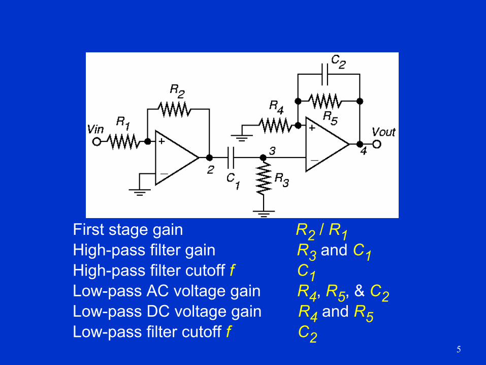
An Example
Consider an amplification circuit:First amplification stage comprises R1, R2 and the first OPAMP.Second stage is a high pass filter comprising of C1 and R3.Third stage is a low-pass filter comprising of R4, R5, C2 and the second OPAMP.
The functional parameters of interest during test are shown on next slide.
Only two of these are single parametric faults.Remaining ones are multiple parametric faults.
5
First stage gain R2 / R1High-pass filter gain R3 and C1High-pass filter cutoff f C1Low-pass AC voltage gain R4, R5, & C2Low-pass DC voltage gain R4 and R5Low-pass filter cutoff f C2

6
Basic Idea
In DSP-based analog testing, no analog fault models were used.Here, we use the fault models, and tests are generated for “specific” multiple faults.Present status:
DSP-based testing remains the most important.Structural testing method gaining acceptance as a supplement to the DSP-based methods.
7
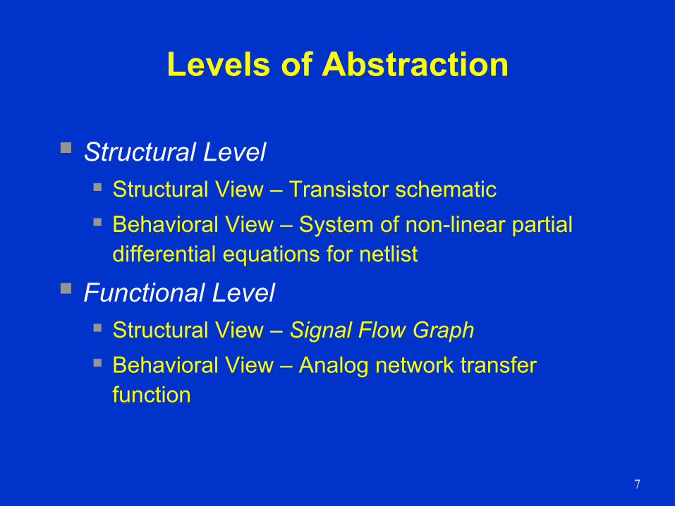
Levels of Abstraction
Structural LevelStructural View – Transistor schematicBehavioral View – System of non-linear partial differential equations for netlist
Functional LevelStructural View – Signal Flow GraphBehavioral View – Analog network transfer function

8
Analog Test Types
Specifications:There is no general design technique for all analog circuits.No universal set of performance specifications.
Tests can be classified into three categories:Design characterization – Does design meet specifications?Diagnostic – Find cause of failuresProduction tests – Test large numbers of linear or mixed-signal circuits
9
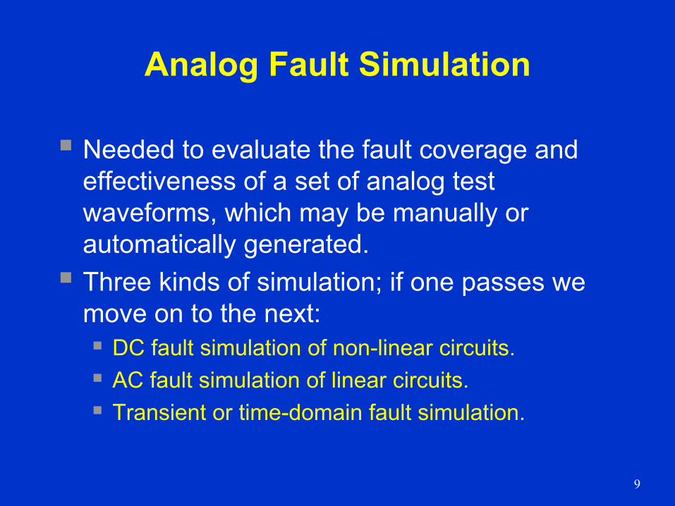
Analog Fault Simulation
Needed to evaluate the fault coverage and effectiveness of a set of analog test waveforms, which may be manually or automatically generated.Three kinds of simulation; if one passes we move on to the next:
DC fault simulation of non-linear circuits.AC fault simulation of linear circuits.Transient or time-domain fault simulation.
10
DC Analog Fault Simulation of Nonlinear Circuits

11
Introduction
DC testing of analog circuits is attractive, since it requires less expensive testers and less testing time.
Useful to analyze how well a DC test can detect a given fault list.Done by solving a set of non-linear equations using PSPICE, which converges after many iterations.Several techniques reduce fault simulation CPU time while improving convergence.

12
Motivation for Analog Fault Simulation
At present, no viable analog circuit synthesis tools exist.
Analog design done manually by experienced designers, using rules of thumb.Analog fault simulation is extremely useful for what-if analysis.
What would happen if the value of R3 is out of the specification by 3%?
Analog fault simulation is far more computationally intensive than ordinary analog circuit simulation.
13
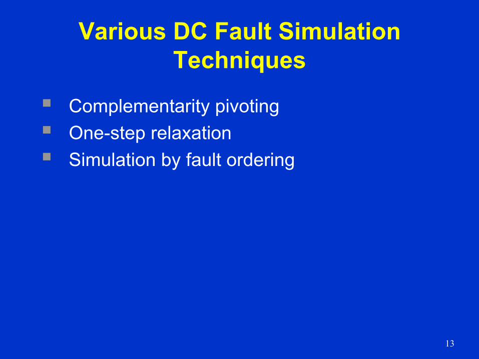
Various DC Fault Simulation Techniques
Complementarity pivotingOne-step relaxationSimulation by fault ordering
14
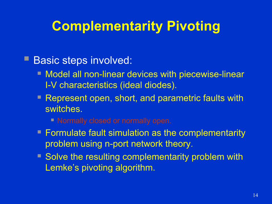
Complementarity Pivoting
Basic steps involved:Model all non-linear devices with piecewise-linear I-V characteristics (ideal diodes).Represent open, short, and parametric faults with switches.
Normally closed or normally open.
Formulate fault simulation as the complementarityproblem using n-port network theory.Solve the resulting complementarity problem with Lemke’s pivoting algorithm.
15
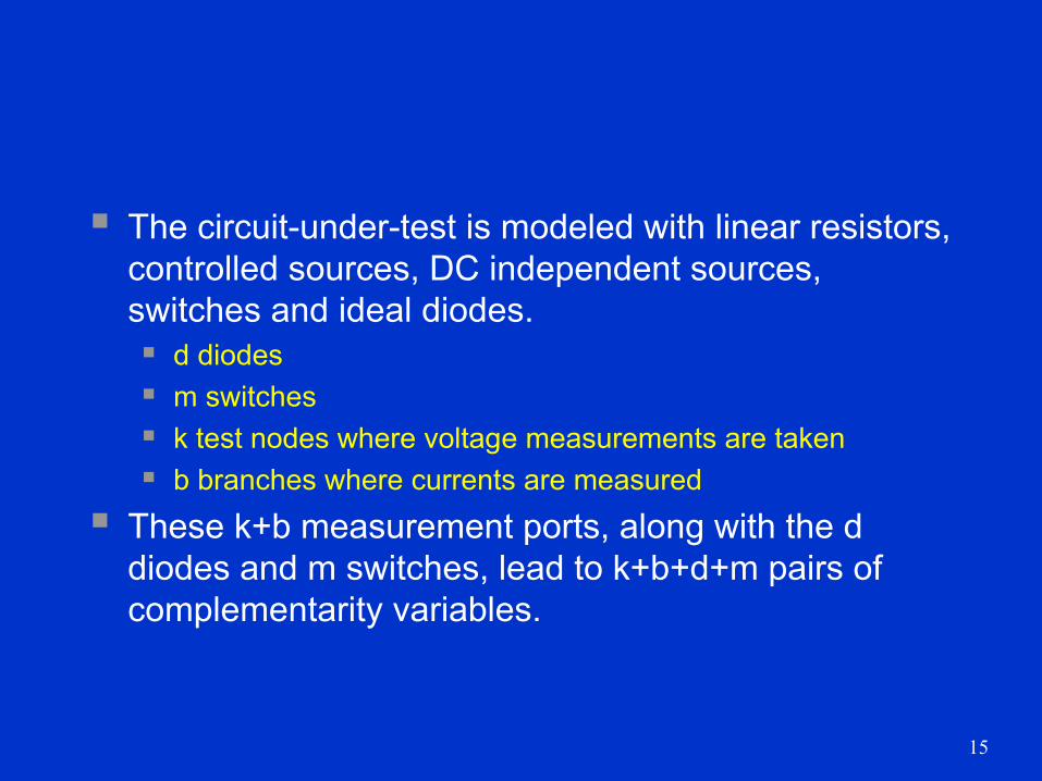
The circuit-under-test is modeled with linear resistors, controlled sources, DC independent sources, switches and ideal diodes.
d diodesm switchesk test nodes where voltage measurements are takenb branches where currents are measured
These k+b measurement ports, along with the d diodes and m switches, lead to k+b+d+m pairs of complementarity variables.
16
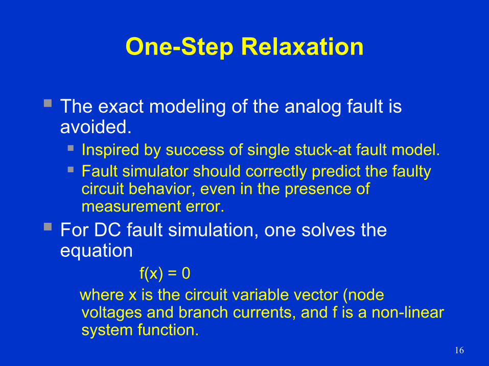
One-Step Relaxation
The exact modeling of the analog fault is avoided.
Inspired by success of single stuck-at fault model.Fault simulator should correctly predict the faulty circuit behavior, even in the presence of measurement error.
For DC fault simulation, one solves the equation
f(x) = 0where x is the circuit variable vector (node voltages and branch currents, and f is a non-linear system function.

17
In Spice, N-R iteration solves the equation iteratively.
Start with initial point x(0) and iterating until the difference between x(k) and x(k+1) converges.
The exact algorithm is:Guess x (0).Solve J(x(k))(x(k+1)-x(k)) = -f(x(k)), for k=0,1,2,… until it converges.J(x(k)) is the Jacobian matrix of f(x(k)).
18
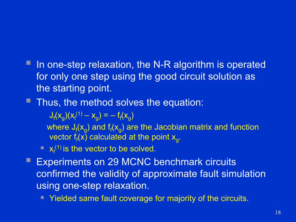
In one-step relaxation, the N-R algorithm is operated for only one step using the good circuit solution as the starting point.Thus, the method solves the equation:
Jf(xg)(xf(1) – xg) = – ff(xg)
where Jf(xg) and ff(xg) are the Jacobian matrix and function vector ff(x) calculated at the point xg.xf
(1) is the vector to be solved.
Experiments on 29 MCNC benchmark circuits confirmed the validity of approximate fault simulation using one-step relaxation.
Yielded same fault coverage for majority of the circuits.

19
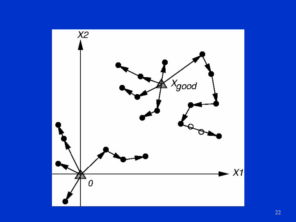
Simulation by Fault Ordering
Fault ordering:Improves simulation convergence, and reduce the number of iterations required by N-R iteration for exact DC fault simulation.Convergence speed depends critically on the starting point.
Basic idea:Order faults so that the results of one simulation becomes a “good” starting point for the next simulation.
20
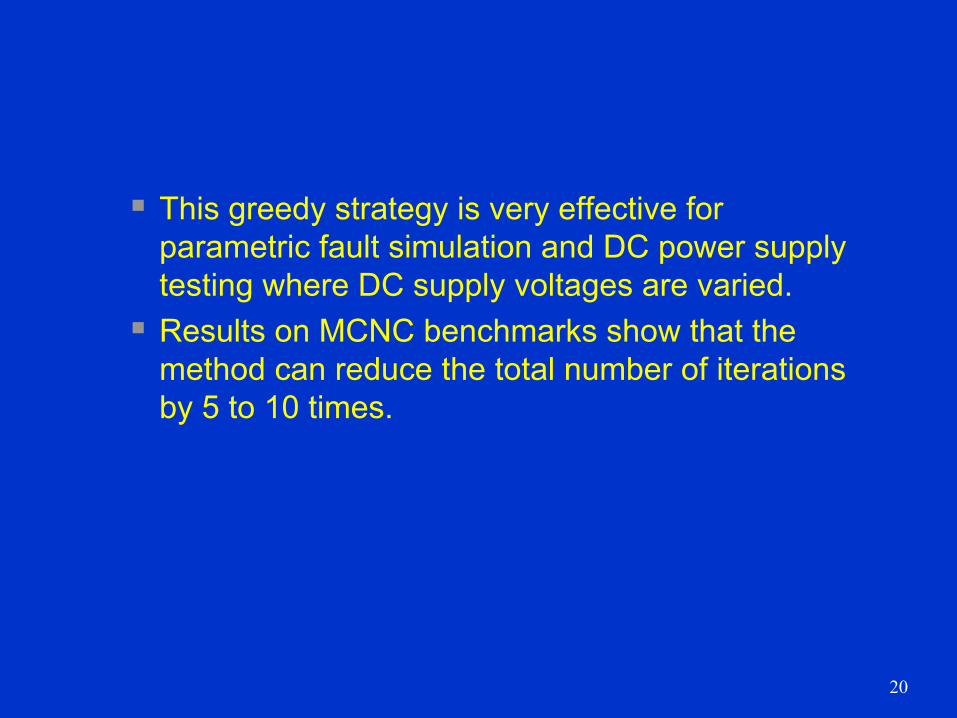
This greedy strategy is very effective for parametric fault simulation and DC power supply testing where DC supply voltages are varied.Results on MCNC benchmarks show that the method can reduce the total number of iterations by 5 to 10 times.
21
Approach by Tian & Shi:Order the fault list so that the result from one fault simulation reduces the number of iterations for simulating the next fault.They use a simple greedy heuristic to order the faults.
22
23
AC Fault Simulation
24
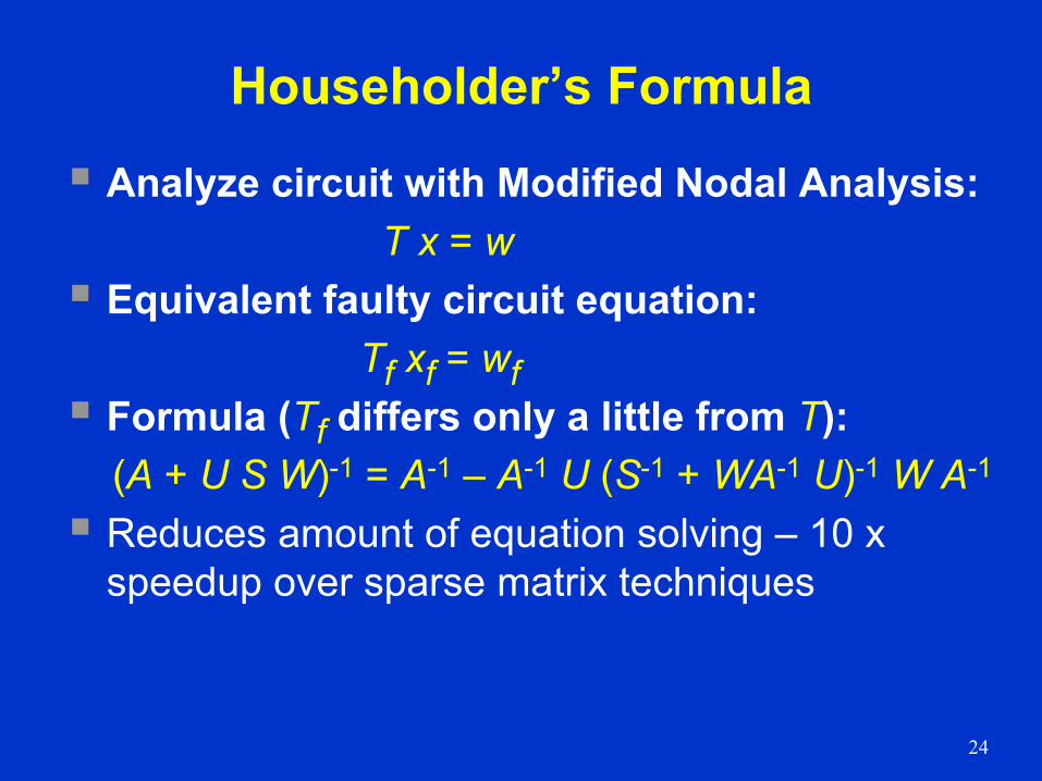
Householder’s Formula
Analyze circuit with Modified Nodal Analysis: T x = w
Equivalent faulty circuit equation:Tf xf = wf
Formula (Tf differs only a little from T):(A + U S W)-1 = A-1 – A-1 U (S-1 + WA-1 U)-1 W A-1
Reduces amount of equation solving – 10 x speedup over sparse matrix techniques
25
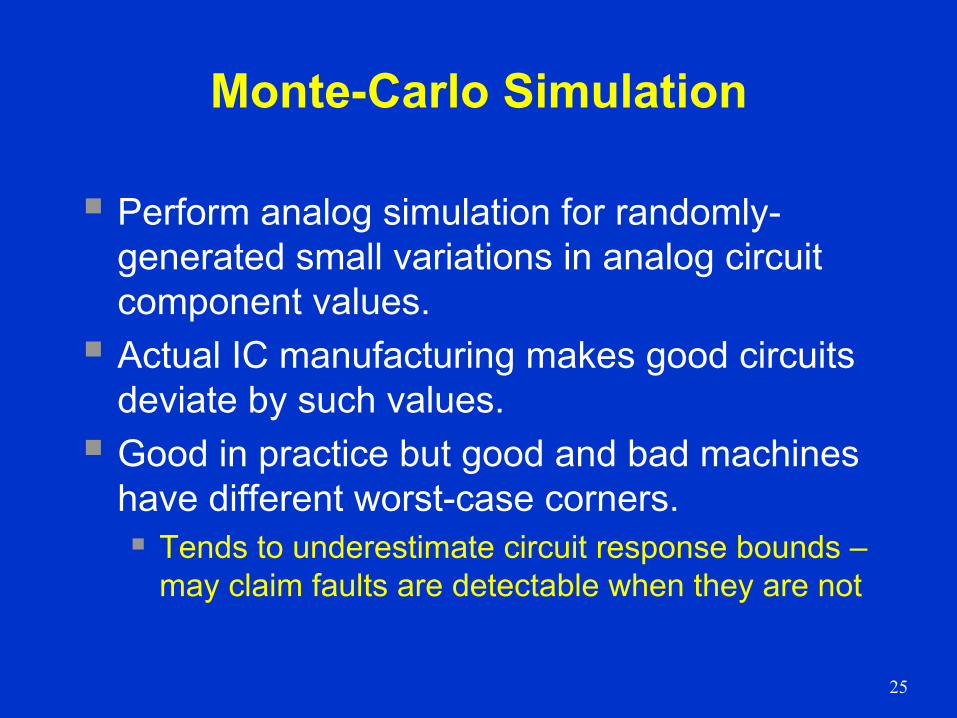
Monte-Carlo Simulation
Perform analog simulation for randomly-generated small variations in analog circuit component values.Actual IC manufacturing makes good circuits deviate by such values.Good in practice but good and bad machines have different worst-case corners.
Tends to underestimate circuit response bounds –may claim faults are detectable when they are not

26
Analog Automatic Test-Pattern Generation
27
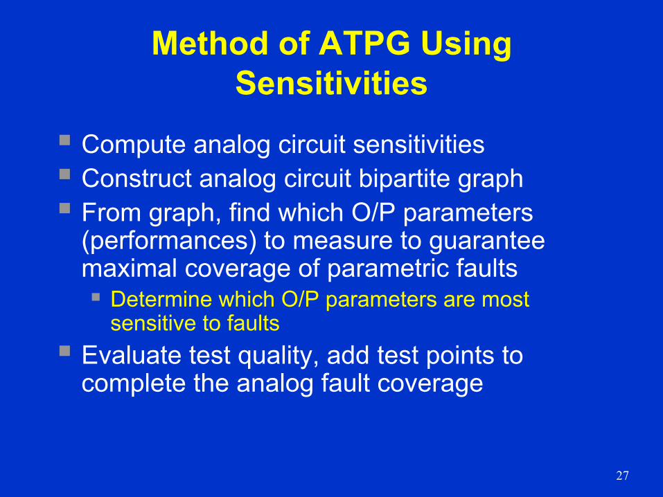
Method of ATPG Using Sensitivities
Compute analog circuit sensitivitiesConstruct analog circuit bipartite graphFrom graph, find which O/P parameters (performances) to measure to guarantee maximal coverage of parametric faults
Determine which O/P parameters are most sensitive to faults
Evaluate test quality, add test points to complete the analog fault coverage

28
Sensitivity
Differential:
S =
Incremental:
ρ = x
Tj – performance parameterxi – network element
Tj
xi
xi Tj
Tj xi
∆ Tj / Tj
∆ xi / xi ∆ xi 0
Tj
xi
xi
Tj
∆ Tj
∆ xi
∂∂

29
Circuit Model

30
Incremental Sensitivity Matrix of Circuit
-0.9100000
R1
100000
R2
00.58-0.91
000
C1
00.38-0.89
000
R3
000
-0.96-0.97
0R4
000
0.48-0.97-0.88R5
000
-0.480
-0.91C2
A1A2fc1A3A4fc2

31
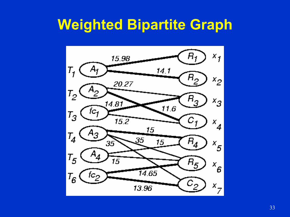
Bipartite Graph of Circuit

32
Single Fault Best and Worst-Case Deviations
A1
A2
A4
5 15.98
5 14.1
5 20.27
5 11.6
5 15
5 15
≤
≤
≤
≤
≤
≤
≤
≤
≤
≤
≤
≤
∆R1R1∆R2R2∆R3R3∆C1C1∆R4R4∆R5R5
fc1
fc2
A3
5 14.81
5 15.2
5 14.65
5 13.96
5 15
5 35
5 35
≤
≤
≤
≤
≤
≤
≤
∆R3R3∆C1C1∆R5R5∆C2C2∆R4R4∆R5R5∆C2C2
≤
≤
≤
≤
≤
≤
≤
33
Weighted Bipartite Graph
34
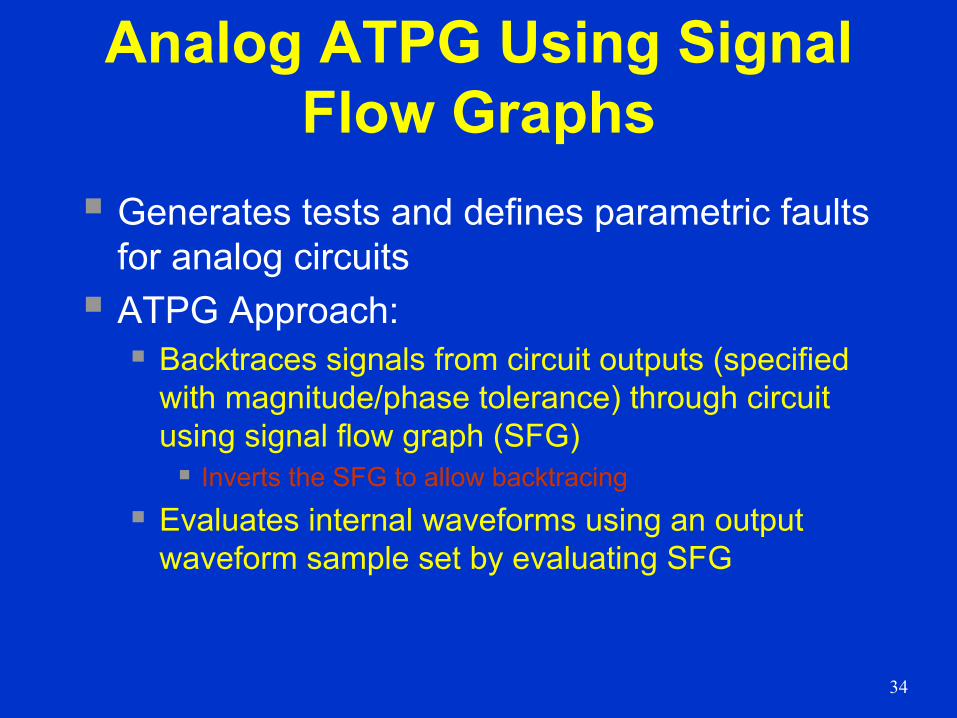
Generates tests and defines parametric faults for analog circuitsATPG Approach:
Backtraces signals from circuit outputs (specified with magnitude/phase tolerance) through circuit using signal flow graph (SFG)
Inverts the SFG to allow backtracing
Evaluates internal waveforms using an output waveform sample set by evaluating SFG
Analog ATPG Using Signal Flow Graphs

35
Test Generation via Reverse Simulation
Find good circuit signal values at all nodes using good output waveformFind bad circuit signal values at all nodes using bad output waveform (use extrema of tolerance box for magnitude or phase)Finds faulty value of analog component necessary to drive output waveform out of tolerance box
Mark all corresponding edges to faultCompute modified SFG weights that give good value after bad edges in inverted SFG

36
Integrator Example
Basic integrator circuit with ideal OPAMP
37
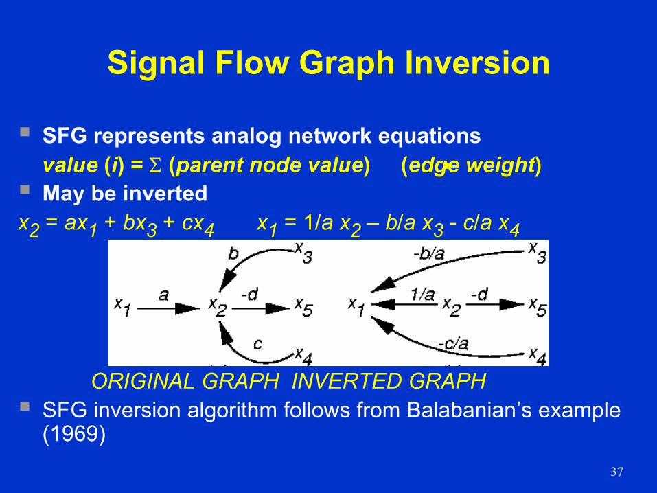
Signal Flow Graph Inversion
SFG represents analog network equationsvalue (i) = Σ (parent node value) (edge weight)May be inverted
x2 = ax1 + bx3 + cx4 x1 = 1/a x2 – b/a x3 - c/a x4
ORIGINAL GRAPH INVERTED GRAPHSFG inversion algorithm follows from Balabanian’s example (1969)

38
SFG Inversion Algorithm
Start at a primary input, x1, a source nodeReverse the direction of the outgoing edge from x1to x2 and change the weight to 1/aRedirect all edges incident on x2 to x1 and change weights appropriatelyContinue for all source nodes, from all inputs, until the output becomes a source
Inverted SFG Properties:Equivalent to original SFGA feed-forward network – graph cycles cutRepresents set of integral equations, solved by numerical differentiationMay be an unstable system
39
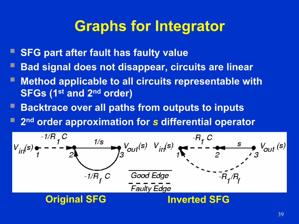
Graphs for Integrator
Original SFG Inverted SFG
SFG part after fault has faulty valueBad signal does not disappear, circuits are linearMethod applicable to all circuits representable with SFGs (1st and 2nd order)Backtrace over all paths from outputs to inputs2nd order approximation for s differential operator

40
Analog Fault Definition
Want to find parametric fault value for R1Use good & bad node values for all nodes from reverse analog simulationFor parametric fault definition in inverted SFG
Use good values for nodes before faultUse bad values for nodes after faultLinear equation in 1 variable for each componentManipulate component equations symbolically to get component tolerance

41
Calculation of R1 Tolerance to Cause Fault
goodval (1) badval (3)-R1 C -Rf C
badval (R1) - goodval (1)C (badval (2) + badval (3) / Rf C)
goodval (R1) - goodval (1)C (goodval (2) + goodval (3) / Rf C)
R1 Tolerance = goodval (R1) – badval (R1)
+ = badval (2)
=
=
Inverted SFGOriginal SFG
42
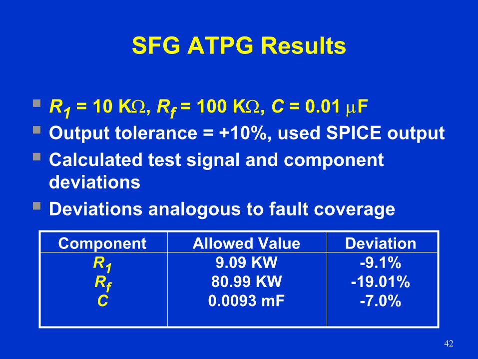
SFG ATPG Results
R1 = 10 KΩ, Rf = 100 KΩ, C = 0.01 µFOutput tolerance = +10%, used SPICE outputCalculated test signal and component deviationsDeviations analogous to fault coverage
ComponentR1RfC
Allowed Value9.09 KW80.99 KW0.0093 mF
Deviation-9.1%
-19.01%-7.0%
43
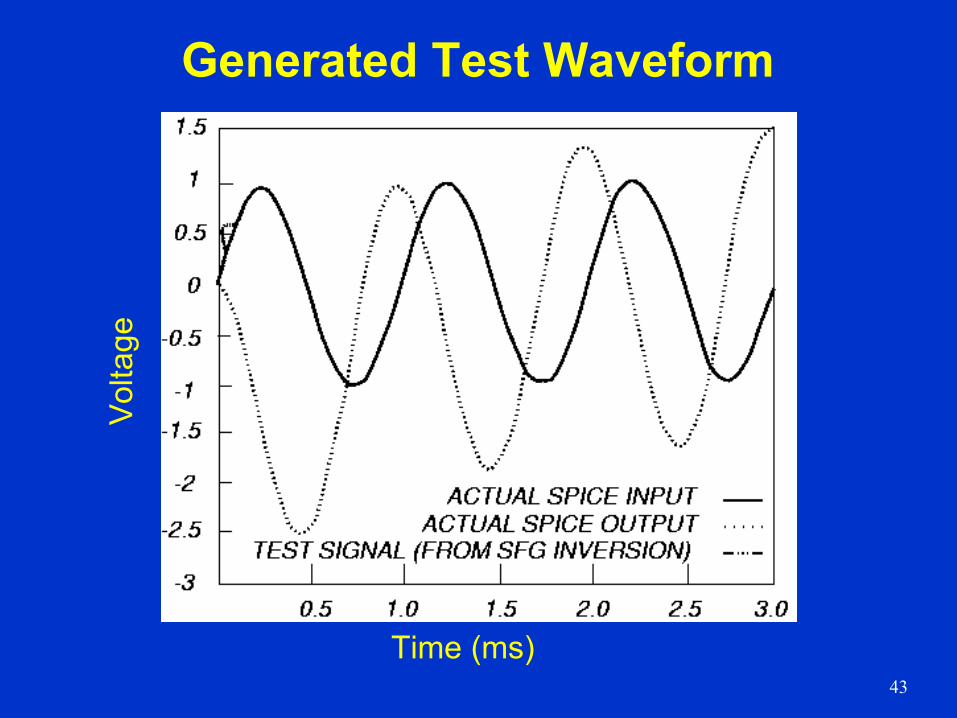
Generated Test WaveformV
olta
ge
Time (ms)
44
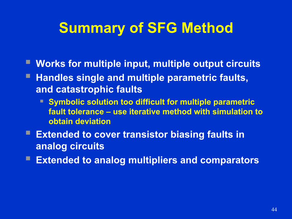
Summary of SFG Method
Works for multiple input, multiple output circuitsHandles single and multiple parametric faults, and catastrophic faults
Symbolic solution too difficult for multiple parametric fault tolerance – use iterative method with simulation to obtain deviation
Extended to cover transistor biasing faults in analog circuitsExtended to analog multipliers and comparators
45
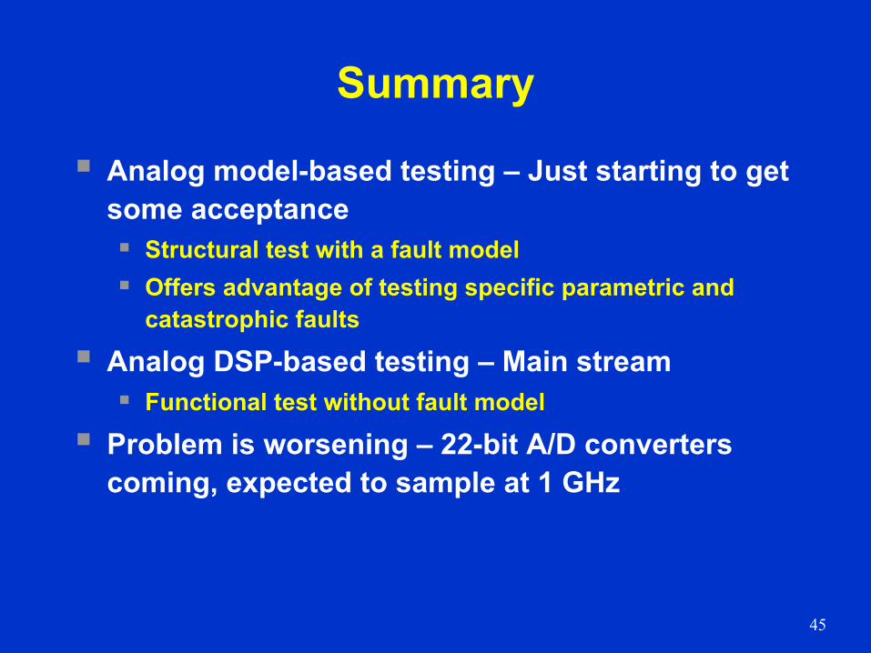
Summary
Analog model-based testing – Just starting to get some acceptance
Structural test with a fault modelOffers advantage of testing specific parametric and catastrophic faults
Analog DSP-based testing – Main streamFunctional test without fault model
Problem is worsening – 22-bit A/D converters coming, expected to sample at 1 GHz