Embed Size (px)
Citation preview

Fault-Tolerant Delay-Insensitive
Communication
A thesis submitted to the University of Manchester
for the degree of Doctor of Philosophy in the
Faculty of Engineering and Physical Sciences
2010
Yebin Shi
School of Computer Science
2
Contents
Chapter 1 Introduction ........................................................................................................ 14
1.1 Unreliability in modern VLSI ............................................................................. 14
1.2 Transient faults ................................................................................................... 17
1.3 Fault tolerance techniques in asynchronous circuits ......................................... 18
1.4 Research aims and contributions ........................................................................ 19
1.5 Thesis overview .................................................................................................. 21
1.6 Publications ........................................................................................................ 22
Chapter 2 Asynchronous circuit and pipeline design .......................................................... 23
2.1 Introduction ........................................................................................................ 23
2.2 Fundamentals of asynchronous circuits .............................................................. 24
2.2.1 Handshake protocols ...................................................................................... 24
2.2.2 Classification of asynchronous circuits ......................................................... 25
2.2.3 Data encoding ................................................................................................ 26
2.3 Asynchronous circuit implementations .............................................................. 27
2.3.1 Static data-flow structure ............................................................................... 27
2.3.2 fundamental elements .................................................................................... 29
2.3.3 Combinational logic design ........................................................................... 31
2.4 Asynchronous pipelines ...................................................................................... 32
2.4.1 Muller pipeline .............................................................................................. 32
2.4.2 2-phase bundled data pipeline – Micropipeline ............................................. 33
2.4.3 A simplified 2-phase bundled data pipeline – Mousetrap .............................. 35
2.4.4 4-phase bundled data pipeline ....................................................................... 36
2.4.5 4-phase dual-rail pipeline .............................................................................. 37
2.5 Asynchronous on-chip systems .......................................................................... 38
2.5.1 Global asynchronous Local synchronous (GALS) ........................................ 38
2.5.2 Network on-chip (NoC) and asynchronous NoC ........................................... 40
2.6 Global DI communication .................................................................................. 42
2.6.1 1-of-4 pipeline ............................................................................................... 42
2.6.2 m-of-n pipeline .............................................................................................. 43
2.7 Summary ............................................................................................................. 45
Chapter 3 Asynchronous Network-on-Chip – SpiNNaker .................................................. 46
3.1 SpiNNaker - hardware simulation platform for Spiking Neuron Network ......... 46
3.2 Micro-processor sub-system ............................................................................... 48
3.3.1 DMA controller.............................................................................................. 49
3.3.2 Communication controller ............................................................................. 49
3.3 Communication in many core systems of SpiNNaker ........................................ 50
3.3.1 On-chip shared bus architecture .................................................................... 50
3.3.2 System NoC - CHAIN ................................................................................... 54
3.3.3 Communications NoC ................................................................................... 55
3.3.4 Router ............................................................................................................ 56
3.3.5 Input and output sections ............................................................................... 58
3.3.6 Off-chip networking ...................................................................................... 58
3
3.4 Neural traffic load at on- and off-chip Network ................................................. 59
3.5 Fault tolerance requirements in SpiNNaker ........................................................ 63
3.6 Summary ............................................................................................................. 66
Chapter 4 Asynchronous interconnect implementation in SpiNNaker................................ 67
4.1 Overview ............................................................................................................ 67
4.2 DI codes in SpiNNaker interconnects ................................................................. 69
4.2.1 On-chip DI codes ........................................................................................... 69
4.2.2 Membership test ............................................................................................ 71
4.2.3 Code selection ............................................................................................... 72
4.2.4 Code conversion ............................................................................................ 74
4.3 Phase conversions in interface circuits ............................................................... 75
4.4 Transmitter implementation ................................................................................ 76
4.4.1 Data channel .................................................................................................. 77
4.4.2 Control channel.............................................................................................. 79
4.5 Receiver implementation .................................................................................... 81
4.5.1 Data channel .................................................................................................. 83
4.5.2 Control channel.............................................................................................. 83
4.6 Analysis of timing assumptions .......................................................................... 86
4.7 Summary ............................................................................................................. 88
Chapter 5 Fault tolerance analysis of global DI pipelines ................................................... 89
5.1 Fault sensitivity of C-gates ................................................................................. 89
5.2 Fault sensitivity of 4-phase DI pipelines ............................................................ 90
5.2.1 Dual-rail pipelines based on C-gates ............................................................. 90
5.2.2 1-of-4 pipelines .............................................................................................. 95
5.2.3 m-of-n pipelines ............................................................................................. 96
5.3 Fault sensitivity of 2-phase pipelines.................................................................. 98
5.3.1 Micriopipelines .............................................................................................. 98
5.3.2 Mousetrap pipelines ....................................................................................... 99
5.4 Fault sensitivity of the off-chip interface .......................................................... 100
5.4.1 Completion detector and data converter ...................................................... 100
5.4.2 4-phase to 2-phase converter ....................................................................... 101
5.4.3 2-phase to 4-phase converters ...................................................................... 102
5.5 Summary ........................................................................................................... 106
Chapter 6 Level-Encoded Transition Signalling (LETS) system ...................................... 107
6.1 Level-Encoded Dual-rail (LEDR) .................................................................... 107
6.2 1-of-4 LETS ...................................................................................................... 110
6.3 2-of-7 LETS ...................................................................................................... 113
6.4 Transmitter implementation of 2-of-7 LETS .................................................... 118
6.4.1 3-of-6 decoder.............................................................................................. 118
6.4.2 2-of-7 LETS encoder ................................................................................... 119
6.4.3 Transmitter ................................................................................................... 120
6.5 Implementation of 2-of-7 LETS receiver ......................................................... 122
6.5.1 2-of-7 LETS decoder ................................................................................... 122
6.5.2 3-of-6 encoder.............................................................................................. 123
4
6.5.3 Receiver ....................................................................................................... 123
6.6 Implementation supporting EoP symbols ......................................................... 124
6.6.1 EoP problem ................................................................................................ 124
6.6.2 Revised interface circuits ............................................................................. 126
6.7 Summary ........................................................................................................... 128
Chapter 7 Implementation based on transition insensitive phase converters .................... 129
7.1 Transition insensitive phase converter .............................................................. 129
7.2 Data phase converter in receiver ....................................................................... 133
7.3 Acknowledge phase converter in the transmitter .............................................. 135
7.4 Fault tolerant symbol conversion ...................................................................... 137
7.5 Fault tolerant symbol detection ........................................................................ 139
7.6 Fault tolerant packet transfer - flit counter ....................................................... 140
7.7 Back-pressure issue .......................................................................................... 142
7.8 Fault tolerant receiver architecture ................................................................... 144
7.9 Independent reset scheme ................................................................................. 148
7.10 Summary ........................................................................................................... 150
Chapter 8 Fault simulation results ..................................................................................... 151
8.1 Fault simulation platform ................................................................................. 151
8.1.1 Monitor block .............................................................................................. 152
8.1.2 Data transmitting module ............................................................................ 154
8.1.3 Data receiving block .................................................................................... 155
8.2 Methodology ..................................................................................................... 156
8.3 Simulation results with realistic timing ............................................................ 157
8.4 Area and performance comparisons ................................................................. 158
8.5 Simulation results with generalized glitches and links ..................................... 159
8.5.1 Packet loss rate ............................................................................................ 160
8.5.2 Deadlock rate ............................................................................................... 161
8.6 Summary ........................................................................................................... 163
Chapter 9 Conclusions ...................................................................................................... 164
9.1 Future Work ...................................................................................................... 168
References .......................................................................................................................... 170
5
List of Tables
Table 1 Variability in nanometre Technology .............................................................. 15
Table 2 Dual-rail code ................................................................................................... 27
Table 3 1-of-4 code ........................................................................................................ 27
Table 4 Power consumption in ANOC and DSPIN ..................................................... 41
Table 5 1-of-n codes ...................................................................................................... 43
Table 6 Properties of DI-codes and DIMS implementations ....................................... 44
Table 7 2-of-7 code and 3-of-6 code .............................................................................. 70
Table 8 Code implementation comparisons ................................................................... 73
Table 9 LEDR code ..................................................................................................... 107
Table 10 Quasi-1-hot 1-of-4 LETS .............................................................................. 111
Table 11 2-of-7 LETS encoding .................................................................................. 115
Table 12 Data bits decoding of 2-of-7 code ................................................................. 116
Table 13 Comparisons of LEDR and LETS ................................................................ 116
Table 14 Transmitter Interface ..................................................................................... 117
Table 15 Receiver Interface ......................................................................................... 117
Table 16 2-of-7 LETS of supporting EoP .................................................................... 126
Table 17 2-of-7 decoding including EoP ..................................................................... 126
Table 18 Simulation results for the interface designs .................................................. 157
Table 19 Comparisons of area and performance ......................................................... 159
6
List of Figures
Fig 1 increasing integration on a single chip ............................................................... 14
Fig 2 VLSI technology evolution .................................................................................. 14
Fig 3 Increasing process variations ............................................................................. 15
Fig 4 Comparison of SRAM bit SER with Flops/Latches SER .................................. 16
Fig 5 Glitch injection on an off-chip channel ................................................................ 18
Fig 6 Asynchronous handshake circuit .......................................................................... 24
Fig 7 2-phase handshake circuit .................................................................................... 25
Fig 8 4-phase handshake circuit .................................................................................... 25
Fig 9 Delay-insensitive handshake circuit ..................................................................... 26
Fig 10 A simple data flow of asynchronous circuits .................................................... 28
Fig 11 Join in 4-phase bundled data ............................................................................ 29
Fig 12 Muller C-gate symbol and implementations ...................................................... 29
Fig 13 Symbol and circuit of an asymmetric C-gate ..................................................... 30
Fig 14 Symbol and circuit of another asymmetric C-gate ............................................. 30
Fig 15 Mutex symbol and implementation .................................................................. 30
Fig 16 Toggle and its implementations .......................................................................... 31
Fig 17 Dual-rail DIMS AND gate ............................................................................... 32
Fig 18 Muller pipeline ................................................................................................. 32
Fig 19 2-phase bundled data pipeline – Micropipeline ................................................ 33
Fig 20 Mousetrap pipeline ........................................................................................... 35
Fig 21 Mousetrap pipeline with data processing blocks .............................................. 35
Fig 22 4-phase bundled data pipeline .......................................................................... 36
Fig 23 4-phase bundled pipeline with processing blocks ............................................ 37
Fig 24 4-phase dual-rail pipeline ................................................................................. 38
Fig 25 4-bit wide 4-phase dual-rail pipeline .................................................................. 38
Fig 26 Delay time trend in shrinking technology ........................................................ 41
Fig 27 4-phase 1-of-4 pipeline....................................................................................... 42
Fig 28 12 bit 1-of-4 pipeline .......................................................................................... 43
Fig 29 SpiNNaker system topology ............................................................................... 46
Fig 30 Organization of a SpiNNaker chip ..................................................................... 47
Fig 31 Processor sub-system ......................................................................................... 48
Fig 32 Multi-layer AHB bus architecture ...................................................................... 51
Fig 33 Mixed implementation of AHB and AHB Lite bus ............................................ 52
Fig 34 System NoC architecture .................................................................................. 54
Fig 35 Multicast packet ................................................................................................. 55
Fig 36 Point-to-point packet .......................................................................................... 56
Fig 37 Nearest-neighbour packet ................................................................................... 56
Fig 38 Router data flow ................................................................................................. 57
Fig 39 Modelling neuron propagation delay ............................................................... 61
Fig 40 An off-chip link .................................................................................................. 67
Fig 41 Unidirectional off-chip interface ........................................................................ 69
Fig 42 Completion detection of 2-of-4 code .................................................................. 71
7
Fig 43 Completion detection of 2-of-7 code .................................................................. 72
Fig 44 Completion detection of 3-of-6 code .................................................................. 72
Fig 45 2-phase to 4-phase converter .............................................................................. 75
Fig 46 Transmitter block diagram ................................................................................. 77
Fig 47 Interface timing of transmitter ............................................................................ 77
Fig 48 Converter of 3-of-6 code to 2-of-7 code ............................................................ 78
Fig 49 STG of the control module ................................................................................. 80
Fig 50 Circuit of the control module ............................................................................. 80
Fig 51 Simplified STG of the control module ............................................................... 81
Fig 52 Final circuit of the control module ..................................................................... 81
Fig 53 Receiver block diagram ...................................................................................... 82
Fig 54 Interface timing of receiver ................................................................................ 82
Fig 55 Timing for control symbol generation ................................................................ 85
Fig 56 2-input C-gate in different situations .................................................................. 89
Fig 57 M-input C-gate in different situations ................................................................ 90
Fig 58 Glitches at a C-gate and a latch .......................................................................... 90
Fig 59 Case 1 of dual-rail pipeline ................................................................................ 91
Fig 60 Case 2 of dual-rail pipeline ................................................................................ 92
Fig 61 Multiple-bit dual-rail pipeline ............................................................................ 93
Fig 62 Case 1 of multiple-bit dual-rail pipeline ............................................................. 94
Fig 63 1-of-4 pipeline .................................................................................................... 96
Fig 64 A multiple-bit 1-of-4 pipeline ............................................................................. 96
Fig 65 Deadlock at 2-of-4 pipeline ................................................................................ 97
Fig 66 Glitches on Micropipeline .................................................................................. 98
Fig 67 Short glitches on a Mousetrap pipeline .............................................................. 99
Fig 68 Long glitches on a Mousetrap pipeline .............................................................. 99
Fig 69 CD circuits in a 4-phase pipeline ..................................................................... 101
Fig 70 Code convertor in a 4-phase pipeline ............................................................... 101
Fig 71 Transmitter phase converter ............................................................................. 102
Fig 72 Receiver phase converter ................................................................................. 102
Fig 73 Deadlock timing in the phase converter of a receiver ...................................... 103
Fig 74 An alternative 2-phase to 4-phase converter .................................................... 104
Fig 75 Timing of an alternative 2-phase to 4-phase converter .................................... 105
Fig 76 Deadlock of an alternative phase converter...................................................... 105
Fig 77 Example of LEDR code ................................................................................... 107
Fig 78 Global communication based on LEDR ......................................................... 108
Fig 79 LEDR completion detector ............................................................................. 108
Fig 80 LEDR decoder and encoder ........................................................................... 108
Fig 81 Control module ............................................................................................... 109
Fig 82 4-phase and 2-phase dual-rail channels interface ............................................. 110
Fig 83 Completion of 1-of-4 LETS ............................................................................. 112
Fig 84 1-of-4 LETS decoding .................................................................................... 112
Fig 85 1-of-4 LETS encoding .................................................................................... 113
Fig 86 Symbol format .................................................................................................. 114

8
Fig 87 Off-chip interface using 2-of-7 LETS .............................................................. 117
Fig 88 3-of-6 decoder .................................................................................................. 118
Fig 89 Dual-rail encoder .............................................................................................. 118
Fig 90 2-of-7 LETS Encoder ....................................................................................... 119
Fig 91 Dual-rail full adder ........................................................................................... 120
Fig 92 2-of-7 LETS transmitter ................................................................................... 121
Fig 93 2-of-7 LETS decoder ........................................................................................ 122
Fig 94 3-of-6 encoder .................................................................................................. 123
Fig 95 block diagram of 2-of-7 LETS receiver ........................................................... 124
Fig 96 Revised 2-of-7 LETS transmitter ..................................................................... 127
Fig 97 Revised 2-of-7 LETS decoder .......................................................................... 127
Fig 98 Revised 2-of-7 LETS receiver .......................................................................... 128
Fig 99 Novel phase converter ...................................................................................... 129
Fig 100 New phase converter circuit based on NAND gates ...................................... 130
Fig 101 Phase converter with an active low reset port ................................................ 131
Fig 102 State transition graph of the novel phase converter ........................................ 131
Fig 103 Interface timing of new phase converter ........................................................ 132
Fig 104 New phase converter in the receiver .............................................................. 133
Fig 105 Module clr_gen .............................................................................................. 134
Fig 106 Implementation of module clr_gen ................................................................ 134
Fig 107 Tx phase converter for ack2 ........................................................................... 136
Fig 108 A priority arbiter ............................................................................................. 138
Fig 109 Completion detection of complete 2-of-7 code .............................................. 140
Fig 110 Flit counter ..................................................................................................... 140
Fig 1112 Mod 18 flit counter ....................................................................................... 141
Fig 112 Waveform of the mod 18 flit counter ............................................................. 141
Fig 113 Handshaking between 2-phase and 4-phase domains ..................................... 142
Fig 114 Back-pressure tolerant pipelines ..................................................................... 143
Fig 115 Module rx_ctrl in receiver .............................................................................. 145
Fig 116 Implementation of the module rx_ctrl ............................................................ 146
Fig 117 Receiver without a new architecture .............................................................. 147
Fig 118 2-phase ack2 generation circuit in receiver .................................................... 149
Fig 119 Simulation platform diagram .......................................................................... 152
Fig 120 Monitor block ................................................................................................. 153
Fig 121 Data transmitting Block ................................................................................. 155
Fig 122 Data receiving block....................................................................................... 155
Fig 123 Design and fault simulation flow ................................................................... 156
Fig 124 Timing diagram showing long-glitch fault ..................................................... 158
Fig 125 Packet loss rate of LETS design (link speed: 5ns) ......................................... 160
Fig 126 Packet loss rate per glitch of LETS design (link speed: 5ns) ......................... 160
Fig 127 Packet loss rate per glitch of baseline design ................................................. 161
Fig 128 Deadlock rate of baseline design .................................................................... 162
Fig 129 Deadlock rate of new design .......................................................................... 162
Fig 130 SpiNNaker chip layout ................................................................................... 166
9
Abstract
The SpiNNaker machine is a massively-parallel computer aimed at modelling large-scale
systems of spiking neurons. It employs a large number of multicore processor integrated
circuits in a two-dimensional mesh using asynchronous inter-chip interconnect. Its scale
demands that it be robust to the failure of individual components, and in the course of its
development fault-tolerance techniques have been employed at many levels in its design.
Fault tolerance has also become a major concern for modern VLSI design because
deep-submicron technology is more vulnerable to faults than earlier technologies with
larger feature sizes due to the increased parameter variability that results from
near-atomic scales. Asynchronous interconnect is an alternative to synchronous
interconnect that offers advantages such as low power and low electro-magnetic
interference, and is therefore a promising interconnect solution for SpiNNaker and for
deep-submicron technologies in general. However, asynchronous interconnect suffers
from the problem that any malfunction is likely to result in circuit-level deadlock,
recovery from which can be difficult as both ends of the deadlocked link must coordinate
recovery action.
The work described in this thesis investigates the influence of transient off-chip glitches
on the robustness of the delay-insensitive asynchronous interconnect which is used in the
SpiNNaker project. In addition to packet corruption, deadlock may occur in the presence
of glitches. Techniques are proposed in the off-chip interface circuits to filter glitches,
correct illegal symbols, minimise the occurrence of deadlock and allow independent reset
of the link from either end.
Simulation results demonstrate the effectiveness of these techniques primarily to
minimise the occurrence of deadlock caused by single transient glitches.

10
Declaration
No portion of the work referred to in this thesis has been submitted in support of an
application for another degree or qualification of this or any other university or other
institution of learning.

11
Copyright
i The author of this thesis (including any appendices and/or schedules to this thesis) owns
any copyright in it (the “Copyright”) and s/he has given The University of Manchester the
right to use such Copyright for any administrative, promotional, educational and/or
teaching purposes.
ii Copies of this thesis, either in full or in extracts, may be made only in accordance with
the regulations of the John Rylands University Library of Manchester. Details of these
regulations may be obtained from the Librarian. This page must form part of any such
copies made.
iii The ownership of any patents, designs, trade marks and any and all other intellectual
property rights except for the Copyright (the “Intellectual Property Rights”) and any
reproductions of copyright works, for example graphs and tables (“Reproductions”),
which may be described in this thesis, may not be owned by the author and may be owned
by third parties. Such Intellectual Property Rights and Reproductions cannot and must not
be made available for use without the prior written permission of the owner(s) of the
relevant Intellectual Property Rights and/or Reproductions.
iv Further information on the conditions under which disclosure, publication and
exploitation of this thesis, the Copyright and any Intellectual Property Rights and/or
Reproductions described in it may take place is available from the Head of School of
School of Computer Science (or the Vice-President).

12
Acknowledgements
First I would like to thank my supervisor, Prof. Steve Furber. Without his valuable
guidance and support my research and the thesis would not have been possible.
My advisor Dr. Jim Garside has provided me much advice on the circuit
implementation and improvement and also made a great contribution to my Async‟09
paper. Special thanks to Dr Luis Plana for many useful discussions on my research and
thesis. Thanks to Dr. Viv Woods for proofreading the thesis with Jim and Luis.
Thanks also to Dr. Steve Temple and Dr. Charles Brej for their warm help when I met
any problem on EDA tools and my computer. I also would like to thank every team
member in SpiNNaker, who makes the research work more enjoyable.
Finally, I would like to acknowledge the ORS Grant and the School of Computer
Science for sponsoring my PhD study in the first three years.
13
Glossary
Delay Insensitive (DI): a class of asynchronous circuit that makes no assumptions about
wire or gate delays and is the most robust asynchronous circuit.
Delay Insensitive Minterm Synthesis (DIMS): a commonly used methodology to design
dual-rail circuits.
Deadlock: this arises when an asynchronous circuit stops running due to handshake failures.
DI Pipeline: a pipeline whose handshake circuits between pipeline registers are
implemented in a delay-insensitive style.
Globally Asynchronous Locally Synchronous (GALS): locally clocked modules are
connected together using an asynchronous communication mechanism in an on-chip system.
Membership test: detecting the validity of symbols in a DI code. Also called completion
detection.
Network-on-Chip (NoC): a type of on-chip packet switching infrastructure.
Non-Return-to-Zero (NRZ): a transition-based encoding; also called a 2-phase handshake
protocol.
Phase conversion: conversion between asynchronous 2-phase and 4-phase signals.
Quasi Delay Insensitive (QDI): no timing assumptions are made in this type of circuit
except the assumption relating to isochronic forks.
Receiver (RX): receives off-chip packets comprising 2-phase symbols and converts them to
4-phase before passing them on to the on-chip interconnect.
Return-to-Zero (RTZ): level-based encoding scheme; also called a 4-phase handshake
protocol.
Spacer: used in 4-phase circuits to separate two consecutive data symbols, also called a
„Null‟ and normally represented with zeros.
Transient faults: faults caused by particle strikes, power bounce or crosstalk on off- or
on-chip traces.
Transmitter (TX): converts on-chip 4-phase symbols to 2-phase and sends them to an
off-chip channel.
14
Chapter 1 INTRODUCTION
1.1 UNRELIABILITY IN MODERN VLSI
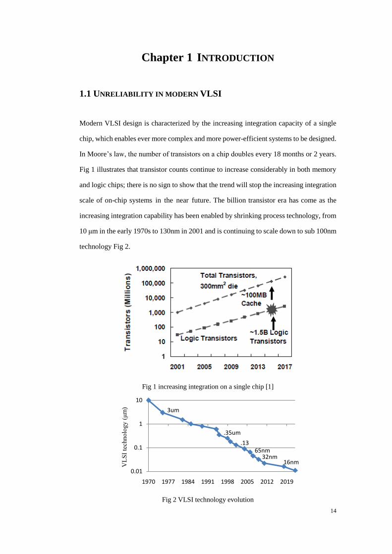
Modern VLSI design is characterized by the increasing integration capacity of a single
chip, which enables ever more complex and more power-efficient systems to be designed.
In Moore‟s law, the number of transistors on a chip doubles every 18 months or 2 years.
Fig 1 illustrates that transistor counts continue to increase considerably in both memory
and logic chips; there is no sign to show that the trend will stop the increasing integration
scale of on-chip systems in the near future. The billion transistor era has come as the
increasing integration capability has been enabled by shrinking process technology, from
10 μm in the early 1970s to 130nm in 2001 and is continuing to scale down to sub 100nm
technology Fig 2.
Fig 1 increasing integration on a single chip [1]
Fig 2 VLSI technology evolution
3um
.35um
.1365nm
32nm16nm
0.01
0.1
1
10
1970 1977 1984 1991 1998 2005 2012 2019
VL
SI
tech
no
logy (
μm
)
15
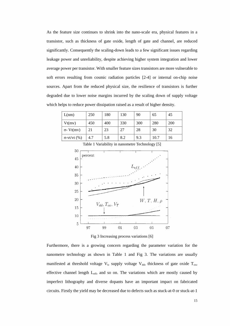
As the feature size continues to shrink into the nano-scale era, physical features in a
transistor, such as thickness of gate oxide, length of gate and channel, are reduced
significantly. Consequently the scaling-down leads to a few significant issues regarding
leakage power and unreliability, despite achieving higher system integration and lower
average power per transistor. With smaller feature sizes transistors are more vulnerable to
soft errors resulting from cosmic radiation particles [2-4] or internal on-chip noise
sources. Apart from the reduced physical size, the resilience of transistors is further
degraded due to lower noise margins incurred by the scaling down of supply voltage
which helps to reduce power dissipation raised as a result of higher density.
L(nm) 250 180 130 90 65 45
Vt(mv) 450 400 330 300 280 200
σ- Vt(mv) 21 23 27 28 30 32
σ-vt/vt (%) 4.7 5.8 8.2 9.3 10.7 16
Table 1 Variability in nanometre Technology [5]
Fig 3 Increasing process variations [6]
Furthermore, there is a growing concern regarding the parameter variation for the
nanometre technology as shown in Table 1 and Fig 3. The variations are usually
manifested at threshold voltage Vt, supply voltage Vdd, thickness of gate oxide Tox,
effective channel length Leff, and so on. The variations which are mostly caused by
imperfect lithography and diverse dopants have an important impact on fabricated
circuits. Firstly the yield may be decreased due to defects such as stuck-at-0 or stuck-at-1
16
faults. Secondly the circuit performance may be degraded significantly due to varied wire
and gate delays and thus worst case designs become expensive. Finally the variability of
physical parameters, such as Vt, Leff, Tox, further compress the noise margin which is
already scaled down with the new technology so that the resistance to transient faults is
weakened.
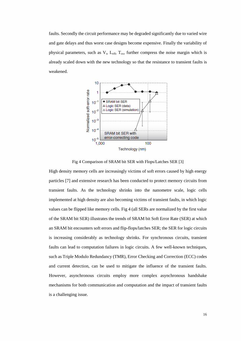
Fig 4 Comparison of SRAM bit SER with Flops/Latches SER [3]
High density memory cells are increasingly victims of soft errors caused by high energy
particles [7] and extensive research has been conducted to protect memory circuits from
transient faults. As the technology shrinks into the nanometre scale, logic cells
implemented at high density are also becoming victims of transient faults, in which logic
values can be flipped like memory cells. Fig 4 (all SERs are normalized by the first value
of the SRAM bit SER) illustrates the trends of SRAM bit Soft Error Rate (SER) at which
an SRAM bit encounters soft errors and flip-flops/latches SER; the SER for logic circuits
is increasing considerably as technology shrinks. For synchronous circuits, transient
faults can lead to computation failures in logic circuits. A few well-known techniques,
such as Triple Modulo Redundancy (TMR), Error Checking and Correction (ECC) codes
and current detection, can be used to mitigate the influence of the transient faults.
However, asynchronous circuits employ more complex asynchronous handshake
mechanisms for both communication and computation and the impact of transient faults
is a challenging issue.
17
1.2 TRANSIENT FAULTS
Modern VLSI circuits may malfunction due to hardware faults, such as manufacturing
faults, intermittent faults, crosstalk, even some faults caused by radiation rays.
Generally, they can be grouped into permanent and transient faults. Permanent faults,
such as stuck-at faults, do not disappear with time; while transient faults, such as
crosstalk or faults caused by radiation rays, only last for a limited time.
Transient faults are of interest for several reasons. First, permanent faults such as stuck-at
faults are often manufacturing defects, and lead to functional failures in synchronous
circuits; these faults can be detected using built-in test circuits, for instance scan chains.
In asynchronous DI circuits, they are also likely to cause functional failures when they
arise in computational circuits; but in handshake circuits, these permanent faults probably
lead to deadlock due to unrecoverable handshake failures. The permanent faults can be
detected effectively during manufacturing tests.
Secondly, another common manufacturing type of faults is a delay fault which leads to a
large delay in a particular circuit path. A timing violation may occur when synchronous
circuits suffer from a delay fault. DI circuits are naturally resistant to these faults due to
their delay insensitivity.
Finally, as far as transient glitches are concerned, they are unpredictable and thus difficult
to detect with conventional testing methods. In synchronous circuits, transient glitches
may cause bit corruptions such as flipped bits in registers or sampling of the wrong data
by registers due to glitches occurring in the combinational circuits that generate their
inputs, or they may even cause metastability. Asynchronous circuits are also potentially
vulnerable to hazards or transient glitches. In the presence of transient faults, handshake
failures may occur and cause deadlock, requiring much effort to identify the deadlock and
recover the application. Thus it is essential to investigate the effects of transient faults on
the global on-chip communication infrastructures.
18
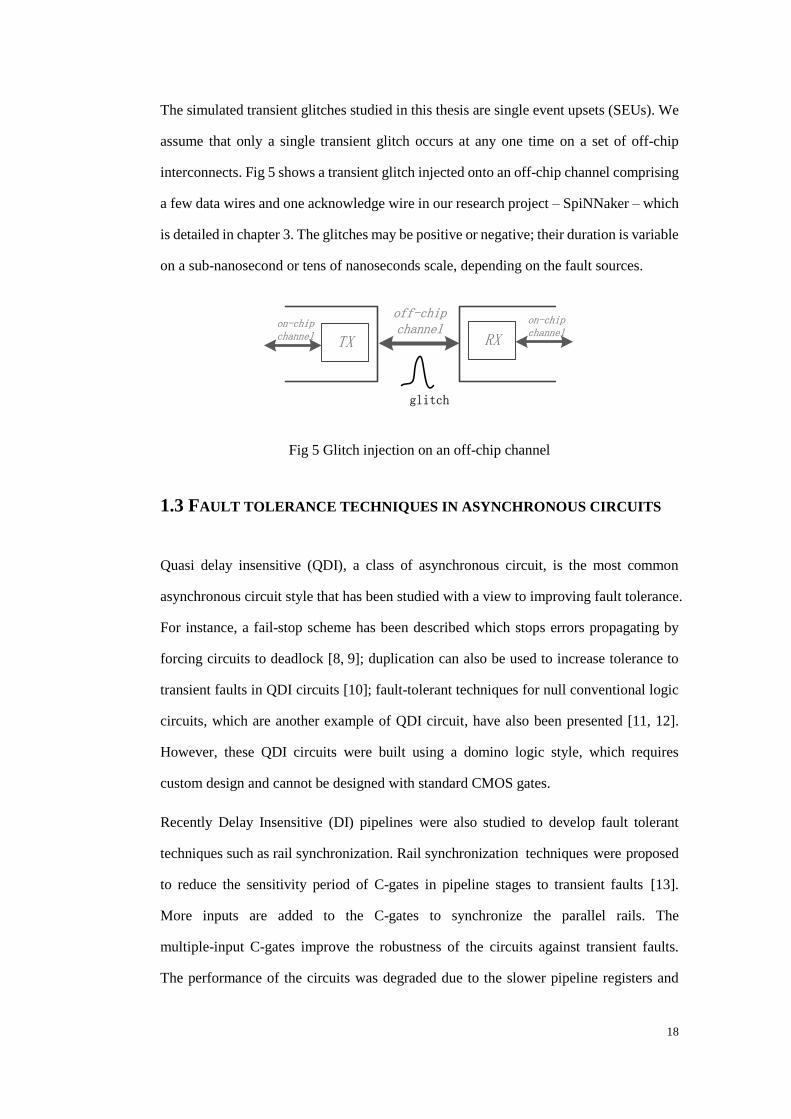
The simulated transient glitches studied in this thesis are single event upsets (SEUs). We
assume that only a single transient glitch occurs at any one time on a set of off-chip
interconnects. Fig 5 shows a transient glitch injected onto an off-chip channel comprising
a few data wires and one acknowledge wire in our research project – SpiNNaker – which
is detailed in chapter 3. The glitches may be positive or negative; their duration is variable
on a sub-nanosecond or tens of nanoseconds scale, depending on the fault sources.
TX RX
off-chip channel
on-chip channel
on-chip channel
glitch
Fig 5 Glitch injection on an off-chip channel
1.3 FAULT TOLERANCE TECHNIQUES IN ASYNCHRONOUS CIRCUITS
Quasi delay insensitive (QDI), a class of asynchronous circuit, is the most common
asynchronous circuit style that has been studied with a view to improving fault tolerance.
For instance, a fail-stop scheme has been described which stops errors propagating by
forcing circuits to deadlock [8, 9]; duplication can also be used to increase tolerance to
transient faults in QDI circuits [10]; fault-tolerant techniques for null conventional logic
circuits, which are another example of QDI circuit, have also been presented [11, 12].
However, these QDI circuits were built using a domino logic style, which requires
custom design and cannot be designed with standard CMOS gates.
Recently Delay Insensitive (DI) pipelines were also studied to develop fault tolerant
techniques such as rail synchronization. Rail synchronization techniques were proposed
to reduce the sensitivity period of C-gates in pipeline stages to transient faults [13].
More inputs are added to the C-gates to synchronize the parallel rails. The
multiple-input C-gates improve the robustness of the circuits against transient faults.
The performance of the circuits was degraded due to the slower pipeline registers and
19
rail synchronization. In addition, the revised circuits were still prone to producing
illegal symbols which then propagate through the downstream circuits.
Developing rail synchronization further, another pipeline latch was introduced to
eliminate illegal symbols [14]. A controller is employed to control two consecutive
pipeline latches by producing two enable signals and to reset the first latch to kill most
of the detected illegal symbols. Thus illegal symbols are unlikely to spread through the
pipeline latches. The enhanced latch further degrades the performance.
A number of fault-tolerance techniques for DI pipelines, all of which are applicable to
asynchronous communication channels exploiting 1-of-n or m-of-n codes, have been
compared in terms of area and performance [15]. These techniques, mainly aiming to
build pipeline latches that are more robust against transient glitches, include input
symbol detection latches, normally closed latches and modified latches that offer
protection against upstream and downstream glitches. Some of these techniques can be
mixed to further improve fault resistance at the cost of high performance penalties.
1.4 RESEARCH AIMS AND CONTRIBUTIONS
As discussed in the previous section, existing techniques make use of duplication or
harden pipeline latches to achieve higher resistance to transient glitches. However, their
penalties in terms of area or performance are high and may be unacceptable in modern
highly-integrated and performance-critical on-chip systems. Another consideration is that
transient faults may impact on system functions differently, such as leading to illegal
symbols, extra and missing normal symbols or even deadlock. Most existing techniques
focus on seeking solutions to detect or eliminate illegal symbols, which are not the only
fault effect but normal symbols can also be induced by transient faults. Deadlock is
more severe than illegal symbols as identifying and removing the deadlock to enable
system recovery is expensive in terms of time, while corrupt data caused by illegal
symbols or extra or missing normal symbols do not stop the circuits from running and
can be detected and possibly even corrected by the system. Thus it is worth expending
20
greater effort to improve the circuit‟s resistance to deadlock. Additionally, most research
has been conducted on single 4-phase circuits, whereas this thesis studies asynchronous
interconnect which involves phase conversion between 2-phase and 4-phase. These
relatively complex circuits motivate the research on their potential deadlock issues.
In this thesis, we focus on approaches to the avoidance of deadlock on global interconnect
which have low performance loss, and then attempt to minimize other fault effects such
as illegal symbols. The high performance penalty found in existing fault-tolerance
techniques prompts us to develop other potential solutions with less performance loss to
increase resistance of our circuits to transient faults.
The primary focus of this research is to investigate the impact of transient glitches on
asynchronous interconnect which provides the global on-chip and off-chip
communication for a large scale system. By injecting a range of glitches with different
durations, the reliability of asynchronous interconnects with a range link speeds are
studied. We target the error effects observed in the current implementation of the off-chip
interconnect and propose techniques to improve the error resilience. The contributions of
this research are as follows:
The development of an implementation of on-chip asynchronous interconnect and
the interface circuit connecting to off-chip channels with conventional asynchronous
circuit design methodology.
The implementation of a simulation model for randomly and extensively injecting
transient glitches to form a fault simulation framework; alternative circuit
implementations can be investigated by exposing them to massively high-density
transient glitches with this framework.
Based on extensive simulation results, a novel fault-tolerant implementation of the
off-chip interface circuits is proposed to avoid the deadlock problem inherent in
conventional asynchronous circuits. This uses a new 2-phase delay-insensitive code,
2-of-7 Level Encoded Transition System (LETS), which exhibits better resistance to
deadlock as it is an inherently fault-tolerant coding.
21
A second implementation makes use of new proposed phase converters to construct
novel interface circuits which overcome the disadvantages of conventional phase
converters. Combined with improved membership test circuits for DI codes and an
arbitration circuit, the novel phase converter shows fault tolerance to transient
glitches with low performance penalty.
1.5 THESIS OVERVIEW
The rest of the thesis is organized as follows. Chapter 2 introduces the fundamental
concepts of asynchronous circuit design and globally asynchronous locally synchronous
(GALS) systems. As they form the infrastructure of global asynchronous communication
some common delay-insensitive pipelines are described, including the Muller pipeline,
Sunderland‟s Micropipeline and other 2-phase and 4-phase pipelines. Finally
delay-insensitive data encoding, including 1-of-n and m-of-n codes, are introduced. The
background of the SpiNNaker project is given in chapter 3, including the motivation for
the project, the processor sub-systems, and the system and communication on-chip
networks. Additionally, a few issues regarding many-core system simulation and neural
network mapping onto the SpiNNaker system are briefly explained.
In chapter 4, an implementation of the interface between the on-chip communication
network and the off-chip channels is implemented as a baseline design using a
conventional design methodology. Chapter 5 discusses fault sensitivity of C-gates and
asynchronous pipelines and the causes of deadlock.
Chapter 6 gives the first fault-tolerant implementation of the interface, which is based on
a novel 2-of-7 data encoding for off-chip channels. Chapter 7 describes a proposed phase
converter which has better fault tolerance given reasonable timing assumptions. A few
techniques, such as modified member test circuits and a symbol arbiter, are also used in
the design to improve the fault tolerance to transient glitches.
Chapter 8 shows the simulation results of the baseline design and the two fault-tolerant
implementations, following fault tolerance requirements in SpiNNaker and fault
22
simulation platform and methodologies.. The simulation results demonstrate the
effectiveness of the resistance to glitches with the realistic timing of the two alternative
designs. Furthermore, the performance and the area costs are also compared for all the
off-chip interface designs. The thesis is concluded in Chapter 9.
1.6 PUBLICATIONS
Y. Shi, S.B. Furber, J. Garside, L. Plana, “Fault Tolerant Delay Insensitive inter-chip
Communication”, Proceedings of the 2009 15th IEEE Symposium on Asynchronous
Circuits and Systems (Async 2009). (Runner-up for the best paper award.)
Y. Shi and S.B. Furber, “Resolving deadlock failures in 2-phase interconnect”, Proc.
19th UK Asynchronous Forum, University of Imperial College, August, 2007.
Y. Shi and S. B. Furber, “Error Checking and Resetting Mechanisms for
Asynchronous Interconnect”, Proc. 18th UK Asynchronous Forum, University of
Newcastle upon Tyne, 2006, pp:24-27, http://async.org.uk/ukasyncforum18/.
S. Yang, S.B. Furber, Y. Shi, L.A. Plana, “An Admission Control System for QoS
Provision on a Best-effort GALS Interconnect”, Proceedings 8th International
Conference on Application of Concurrency to System Design, June 2008, Xi'an,
China.
L. Plana.; J. Bainbridge; S.B. Furber; S. Salisbury; Y. Shi; J. Wu, “An On-Chip and
Inter-Chip Communications Network for the SpiNNaker Massively-Parallel Neural
Net Simulator”, Presented at the Second ACM/IEEE International Symposium on
Networks-on-Chip, 2008. NoCS 2008
L.A Plana, S.B. Furber, S. Temple, M. Khan, Y. Shi, J. Wu, S. Yang, “A GALS
Infrastructure for a Massively Parallel Multiprocessor” IEEE Design & Test of
Computers, Volume: 24, Issue: 5, pp. 454 - 463, Sept.-Oct. 2007.
23
Chapter 2 ASYNCHRONOUS CIRCUIT AND PIPELINE
DESIGN
This chapter reviews some fundamental concepts in asynchronous circuit design. Some
commonly used asynchronous pipelines will be described in detail, including the Muller
pipeline, Micropipelines [16], mousetrap [17] and 1-of-4 CHAIN [18]. Finally global
delay-insensitive (DI) communication is introduced as one promising implementation
option in Globally Asynchronous Locally Synchronous (GALS) systems. In particular,
DI communications based on 1-of-4 and m-of-n DI codes are highlighted.
2.1 INTRODUCTION
Recently, as VLSI technology shrinks and the scale of integration increases, the issues
synchronous designed circuits suffer from are growing significantly. For instance, the
proportion of the power dissipation consumed by the clock signals is increasing
considerably; clock skew effects take more and more design effort to balance the clock
trees; different clock targets originally used in the IP cores lead to difficulties in the
integration of those IP modules in complex SoCs. Therefore asynchronous design
methodology has drawn attention in recent decades by promising to achieve lower power,
higher modularity and even better performance.
Previous work has covered a wide range of topics from design methodologies, automatic
synthesis and testing approaches to silicon demonstration of asynchronous
microprocessors [19-22]. However, it is revealed that asynchronous circuits manifest the
potential of low power and low electromagnetic interference rather than high
performance due to higher area overhead [23]. Furthermore, in the modern large-scale
system-on-chip era asynchronous pipelines can be applied to on-chip global
communication to facilitate highly integrated and low power SoC solutions to resolve the
timing closure issues incurred by global clocks.
24
2.2 FUNDAMENTALS OF ASYNCHRONOUS CIRCUITS
2.2.1 HANDSHAKE PROTOCOLS
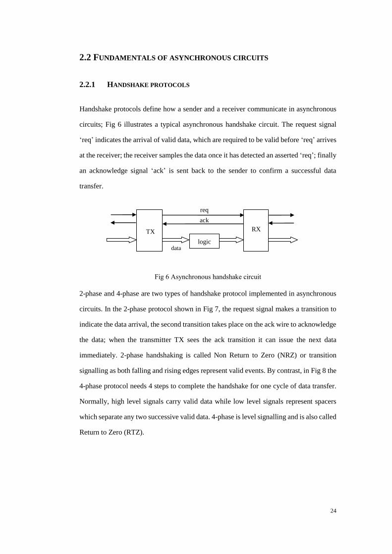
Handshake protocols define how a sender and a receiver communicate in asynchronous
circuits; Fig 6 illustrates a typical asynchronous handshake circuit. The request signal
„req‟ indicates the arrival of valid data, which are required to be valid before „req‟ arrives
at the receiver; the receiver samples the data once it has detected an asserted „req‟; finally
an acknowledge signal „ack‟ is sent back to the sender to confirm a successful data
transfer.
Fig 6 Asynchronous handshake circuit
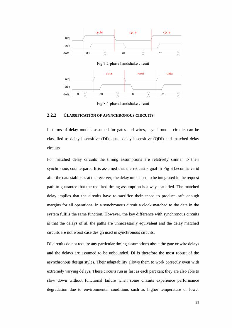
2-phase and 4-phase are two types of handshake protocol implemented in asynchronous
circuits. In the 2-phase protocol shown in Fig 7, the request signal makes a transition to
indicate the data arrival, the second transition takes place on the ack wire to acknowledge
the data; when the transmitter TX sees the ack transition it can issue the next data
immediately. 2-phase handshaking is called Non Return to Zero (NRZ) or transition
signalling as both falling and rising edges represent valid events. By contrast, in Fig 8 the
4-phase protocol needs 4 steps to complete the handshake for one cycle of data transfer.
Normally, high level signals carry valid data while low level signals represent spacers
which separate any two successive valid data. 4-phase is level signalling and is also called
Return to Zero (RTZ).
logic
RX TX
req
ack
data
25
cycle cycle cycle
d0 d1 d2
req
ack
data
Fig 7 2-phase handshake circuit
data reset data
0 d0 0 d1
req
ack
data
Fig 8 4-phase handshake circuit
2.2.2 CLASSIFICATION OF ASYNCHRONOUS CIRCUITS
In terms of delay models assumed for gates and wires, asynchronous circuits can be
classified as delay insensitive (DI), quasi delay insensitive (QDI) and matched delay
circuits.
For matched delay circuits the timing assumptions are relatively similar to their
synchronous counterparts. It is assumed that the request signal in Fig 6 becomes valid
after the data stabilises at the receiver; the delay units need to be integrated in the request
path to guarantee that the required timing assumption is always satisfied. The matched
delay implies that the circuits have to sacrifice their speed to produce safe enough
margins for all operations. In a synchronous circuit a clock matched to the data in the
system fulfils the same function. However, the key difference with synchronous circuits
is that the delays of all the paths are unnecessarily equivalent and the delay matched
circuits are not worst case design used in synchronous circuits.
DI circuits do not require any particular timing assumptions about the gate or wire delays
and the delays are assumed to be unbounded. DI is therefore the most robust of the
asynchronous design styles. Their adaptability allows them to work correctly even with
extremely varying delays. These circuits run as fast as each part can; they are also able to
slow down without functional failure when some circuits experience performance
degradation due to environmental conditions such as higher temperature or lower
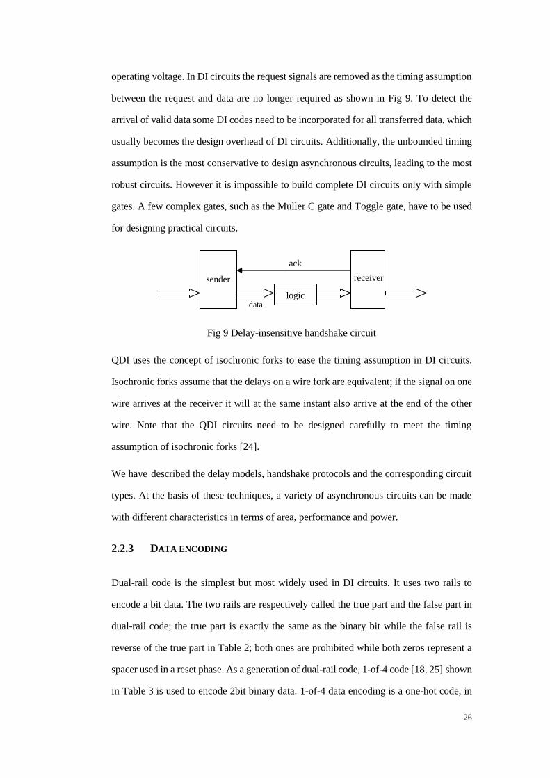
26
operating voltage. In DI circuits the request signals are removed as the timing assumption
between the request and data are no longer required as shown in Fig 9. To detect the
arrival of valid data some DI codes need to be incorporated for all transferred data, which
usually becomes the design overhead of DI circuits. Additionally, the unbounded timing
assumption is the most conservative to design asynchronous circuits, leading to the most
robust circuits. However it is impossible to build complete DI circuits only with simple
gates. A few complex gates, such as the Muller C gate and Toggle gate, have to be used
for designing practical circuits.
Fig 9 Delay-insensitive handshake circuit
QDI uses the concept of isochronic forks to ease the timing assumption in DI circuits.
Isochronic forks assume that the delays on a wire fork are equivalent; if the signal on one
wire arrives at the receiver it will at the same instant also arrive at the end of the other
wire. Note that the QDI circuits need to be designed carefully to meet the timing
assumption of isochronic forks [24].
We have described the delay models, handshake protocols and the corresponding circuit
types. At the basis of these techniques, a variety of asynchronous circuits can be made
with different characteristics in terms of area, performance and power.
2.2.3 DATA ENCODING
Dual-rail code is the simplest but most widely used in DI circuits. It uses two rails to
encode a bit data. The two rails are respectively called the true part and the false part in
dual-rail code; the true part is exactly the same as the binary bit while the false rail is
reverse of the true part in Table 2; both ones are prohibited while both zeros represent a
spacer used in a reset phase. As a generation of dual-rail code, 1-of-4 code [18, 25] shown
in Table 3 is used to encode 2bit binary data. 1-of-4 data encoding is a one-hot code, in
logic
receiver sender
ack
data
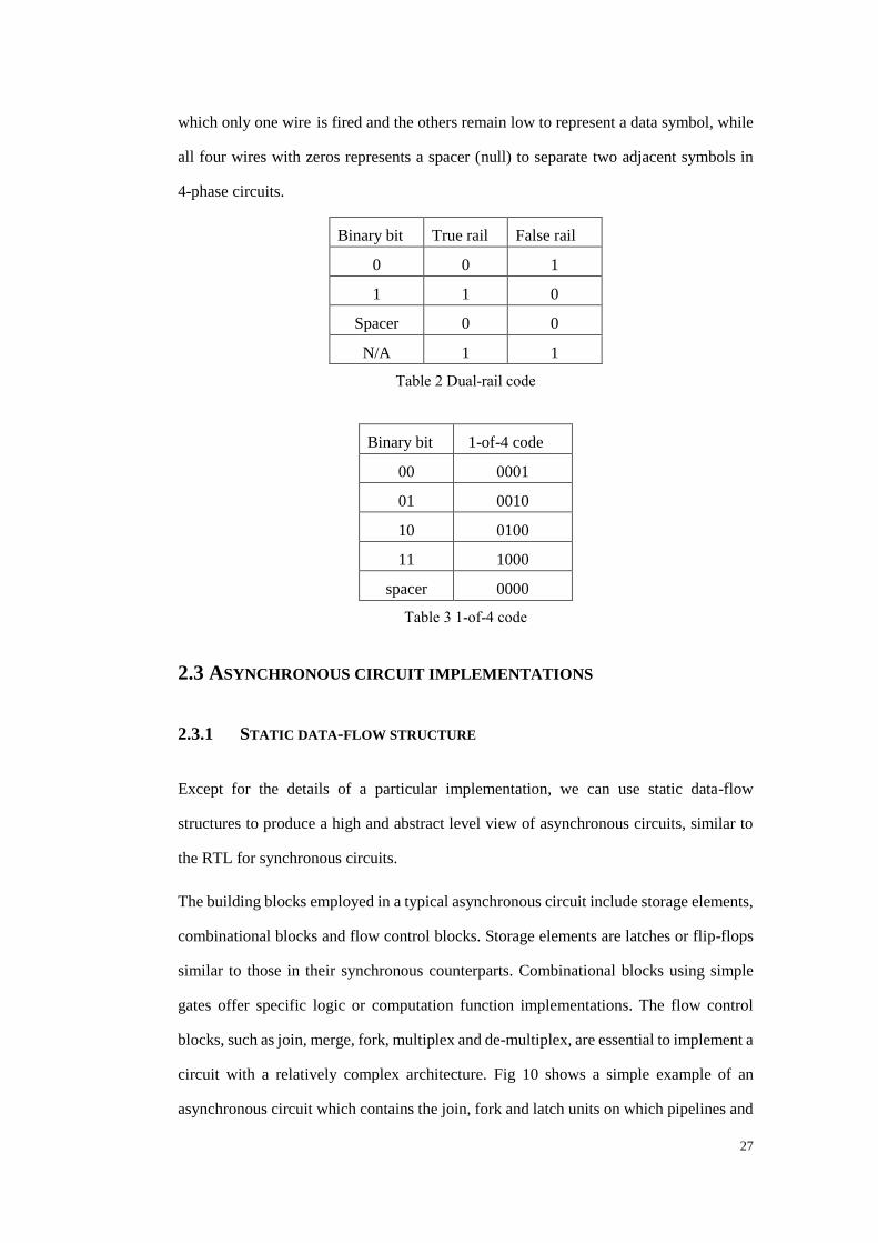
27
which only one wire is fired and the others remain low to represent a data symbol, while
all four wires with zeros represents a spacer (null) to separate two adjacent symbols in
4-phase circuits.
Binary bit True rail False rail
0 0 1
1 1 0
Spacer 0 0
N/A 1 1
Table 2 Dual-rail code
Binary bit 1-of-4 code
00 0001
01 0010
10 0100
11 1000
spacer 0000
Table 3 1-of-4 code
2.3 ASYNCHRONOUS CIRCUIT IMPLEMENTATIONS
2.3.1 STATIC DATA-FLOW STRUCTURE
Except for the details of a particular implementation, we can use static data-flow
structures to produce a high and abstract level view of asynchronous circuits, similar to
the RTL for synchronous circuits.
The building blocks employed in a typical asynchronous circuit include storage elements,
combinational blocks and flow control blocks. Storage elements are latches or flip-flops
similar to those in their synchronous counterparts. Combinational blocks using simple
gates offer specific logic or computation function implementations. The flow control
blocks, such as join, merge, fork, multiplex and de-multiplex, are essential to implement a
circuit with a relatively complex architecture. Fig 10 shows a simple example of an
asynchronous circuit which contains the join, fork and latch units on which pipelines and
28
rings are built. Obviously combinational blocks can be inserted between any two latches
to support more complex computation applications.
Fig 10 A simple data flow of asynchronous circuits [26]
As far as the implementation details are concerned, these circuit blocks can be
implemented with different design styles. First simple gates to build combination logic
may not be those used in combinational logic blocks of synchronous circuits; instead a set
of special elementary gates needs to be built with the conventional simple gates for
different asynchronous protocols. For instance, in delay matched circuits simple gates
such as AND, OR, NOT gates in the standard libraries can be directly used to implement
combinational blocks while in the dual-rail circuits all the specific elements for
performing logic operations such as AND and OR are required to be implemented and
combinational blocks can then be built with these elements.
Secondly, in flow control units multiplexers and de-multiplexers are the conventional
blocks to conditionally steer data flows. However unconditional flow control elements
for joining or merging two or more data flows may have different implementations based
on different asynchronous design styles. By contrast, the unconditional flow control
concepts of join and merge do not exist in the synchronous domain. Synchronous circuits
assume that each part of the circuit is activated at each clock tick. The asynchronous
system is based on tokens, which means that each part is activated only once the required
tokens arrive at its inputs. For instance, in Fig 11, a join operation in the 4-phase bundled
data circuit, as shown in the upper figure, requires that the output z be activated only
when the two inputs x and y are asserted. In the bottom figure, the join output request
Fork Join
Join Fork
29
signal Z-req can only be activated either by two „valid‟ tokens or by two „empty‟ tokens
indicating two both „valid‟ or both „empty‟ input values at x-req and y-req respectively;
thereby a C-gate needs to be applied to synchronize the token behaviour.
Fig 11 Join in 4-phase bundled data [26]
2.3.2 FUNDAMENTAL ELEMENTS
A few most commonly used elements in asynchronous circuit implementations, such as
the C-gate, Mutex and Toggle, are introduced. The Muller C-gate is an essential element
in asynchronous design; as a state holding gate it does not change its output unless both
inputs are equivalent, which means that it goes high only when both inputs become high
and goes low only when both inputs become low. Fig 12 shows an implementation of
Muller C-gate based on standard gates and the symbol.
CA
BZ
B
AZ
Fig 12 Muller C-gate symbol and implementations
Asymmetric C-gates are derived from the Muller C-gate. Fig 13 illustrates a asymmetric
C-gate which flips its output to high only when both inputs become high while a single
low input „A‟ can turn the output „Z‟ to low directly without a low input „B‟. Other
asymmetric C-gates are also available, another example is shown in Fig 14.
30
+
CA
B
Z
A
B Z
Fig 13 Symbol and circuit of an asymmetric C-gate
-
CA
B
Z
A
BZ
Fig 14 Symbol and circuit of another asymmetric C-gate
When two signals are required to be mutually exclusive, for instance, for access to a
shared resource, an element called a Mutex is introduced. Fig 15 illustrates the symbol
and a possible implementation with NAND gates and transmission gates. The first signal
to arrive at either R1 or R2 leads to the assertion of the corresponding output G1 or G2,
while the other signal is blocked until the first input signal is removed. In the
implementation, there are two NMOS and PMOS transistors connected at the nodes X1
and X2 which are placed to solve the metastability problem. Instead of the transistors,
standard cells like 3-input OR gates are an alternative solution.
Fig 15 Mutex symbol and implementation [26]
A Toggle element alternates its output in response to an input transition and can be used
for converting signals from 4-phase to 2-phase. The first event at the input „i‟ results in an
event at its output „q0‟, while the second input event results in an event at its output „q1‟
and so forth. Fig 16 shows the symbol, a possible D-type flip-flop implementation and a
simplification which can be used to convert signals from 4-phase to 2-phase.
31
Ti q0
q1
Q
QSET
CLR
Dq0
i
Q
QSET
CLR
Dq1
Q
QSET
CLR
Dq0
i
Fig 16 Toggle and its implementations
2.3.3 COMBINATIONAL LOGIC DESIGN
In bundled data circuits, the combinational logic between latches is constructed in the
same manner as in a synchronous circuit where the binary code or single rail is used for
data representation; the only difference between them is the approach used to meet timing
closure. In synchronous circuits, the delay incurred by critical paths determines the clock
frequency. By contrast, in bundled data circuits matched delay units have to be selected
carefully and placed at the request paths according to the actual delays of data paths. As a
result, the delays on the request paths match or exceed the delays taken by the
combinational blocks.
In DI circuits, as all data are encoded with a DI code, the combinational logic circuits
cannot be designed in a similar way to the bundled data circuits based on single-rail.
Delay Insensitive Minterm Synthesis (DIMS) [27] was invented by David Muller to
implement DI logic circuits and in Fig 16, a dual-rail AND gate is illustrated. The
combinational logic is transparent to the handshake circuits, which means that the logic
circuit does not need to generate an acknowledge signal. The combinational circuits must
wait for all inputs valid however to avoid a premature value at its output, similarly it
cannot de-assert its output until all inputs become low. In principle, each required
minterm of input variables is output by a C-gate and the final logic output is formed by
ORing all the required minterms from their corresponding C-gates, as shown in Fig 17.
This synchronization in the combinational blocks makes it much easier to implement the
join and merge structure for dual-rail circuits. Note that DIMS is also applicable for
designing 4-phase DI circuits with 1-of-4 or any other one-hot code.
32
Fig 17 Dual-rail DIMS AND gate [26]
The DIMS approach generates an inefficient solution to DI logic circuits though the
implementation based on DIMS of a complex logic block can be optimized to save logic
gates. Other approaches, such as Spacer Conventional Logic (NCL) [28], are available to
reduce the implementation complexity.
2.4 ASYNCHRONOUS PIPELINES
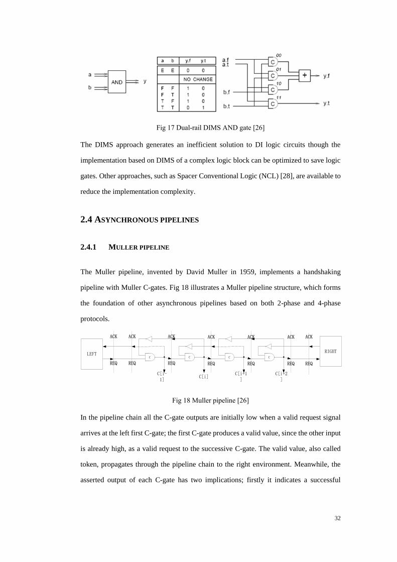
2.4.1 MULLER PIPELINE
The Muller pipeline, invented by David Muller in 1959, implements a handshaking
pipeline with Muller C-gates. Fig 18 illustrates a Muller pipeline structure, which forms
the foundation of other asynchronous pipelines based on both 2-phase and 4-phase
protocols.
C
C[i+2]
C
C[i+1]
C
C[i]
C
C[i-1]
ACK ACK ACK ACK
REQ REQ REQ REQ
ACK
REQ
ACK
REQ
LEFT
ACK
REQ
RIGHT
Fig 18 Muller pipeline [26]
In the pipeline chain all the C-gate outputs are initially low when a valid request signal
arrives at the left first C-gate; the first C-gate produces a valid value, since the other input
is already high, as a valid request to the successive C-gate. The valid value, also called
token, propagates through the pipeline chain to the right environment. Meanwhile, the
asserted output of each C-gate has two implications; firstly it indicates a successful
33
reception of the request token to the left environment; secondly it can be used to turn on,
or off, the data paths.
The elegance existing in the Muller pipeline is not only the symmetrical and regular
layout but also the delay-insensitive property. The throughput of the pipeline is
determined by the actual delay of its gates and wires; if the right environment is unable to
respond to the arriving token the pipeline will eventually stall the left environment.
Finally, the Muller pipeline works perfectly regardless of the protocols used in the control
and data path. The difference in implementations for 4-phase and 2-phase is the
interpretations of the request and acknowledge signals applied for handshaking and
controlling data paths. In 4-phase pipelines those control signals are interpreted as level
signals while they are transition signals in 2-phase pipelines. The following sections
introduce some pipelines which are variants of the Muller pipeline.
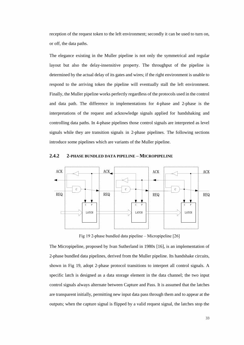
2.4.2 2-PHASE BUNDLED DATA PIPELINE – MICROPIPELINE
Fig 19 2-phase bundled data pipeline – Micropipeline [26]
The Micropipeline, proposed by Ivan Sutherland in 1980s [16], is an implementation of
2-phase bundled data pipelines, derived from the Muller pipeline. Its handshake circuits,
shown in Fig 19, adopt 2-phase protocol transitions to interpret all control signals. A
specific latch is designed as a data storage element in the data channel; the two input
control signals always alternate between Capture and Pass. It is assumed that the latches
are transparent initially, permitting new input data pass through them and to appear at the
outputs; when the capture signal is flipped by a valid request signal, the latches stop the
CC
ACK ACK
REQ REQ
ACK
REQ
LATCH LATCH
C P C P
C
LATCH
C P
ACK
REQ

34
outputs from updating with any change at the inputs; when the pass signal changes its
level due to a valid acknowledge signal, the latches change back to be transparent for new
incoming data. In other words, the latches are transparent when C=P while they hold
without updating output data when C≠P.
Before the pipeline starts to transfer data, all the C-gate outputs are low. The control input
ports C and P of all latches are equivalent which forces them to be transparent, indicating
that the latches are free to sample new data. In the bundled data pipeline, it is assumed
that the delay of every request signal matches (is larger than) the delay on its
corresponding data path. Once the data and the request signal are issued from the left
environment to the first C-gate and latch, the C-gate is ready to assert its output and flip
the C port of the latch to high. The latches are then not able to update their outputs but
hold their values. The matched request delay at the control channel guarantees that data
are captured correctly. In the meantime, a valid ACK signal is issued back to the left
environment by the first pipeline stage, indicating that the first pipeline stage has
succeeded in capturing the data.
Next, the request signal output from the first C-gate propagates to the middle pipeline
stage and stops it sampling from the data channel; meanwhile the output of the middle
C-gate also issues a valid ack signal to the C-gate in the first pipeline stage and then flips
the control signal P to force those latches back to be transparent again.
The 2-phase Micropipeline described above does not involve any data processing.
Similar to the Muller pipeline, in Micropipelines, combinational blocks can be inserted
between two adjacent pipelines stages to implement complex applications. Note that
matched request delays need to be increased to balance the wire delays in the data channel
as well as the delay incurred by the combinational blocks. The 2-phase Micropipeline has
been implemented in Amulet1 [19], demonstrating the feasibility to design complex
asynchronous systems.
35
2.4.3 A SIMPLIFIED 2-PHASE BUNDLED DATA PIPELINE – MOUSETRAP
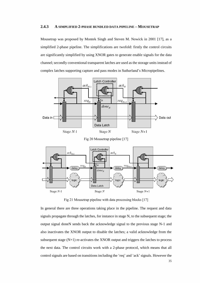
Mousetrap was proposed by Montek Singh and Steven M. Nowick in 2001 [17], as a
simplified 2-phase pipeline. The simplifications are twofold: firstly the control circuits
are significantly simplified by using XNOR gates to generate enable signals for the data
channel; secondly conventional transparent latches are used as the storage units instead of
complex latches supporting capture and pass modes in Sutherland‟s Micropipelines.
Fig 20 Mousetrap pipeline [17]
Fig 21 Mousetrap pipeline with data processing blocks [17]
In general there are three operations taking place in the pipeline. The request and data
signals propagate through the latches, for instance in stage N, to the subsequent stage; the
output signal doneN sends back the acknowledge signal to the previous stage N-1 and
also inactivates the XNOR output to disable the latches; a valid acknowledge from the
subsequent stage (N+1) re-activates the XNOR output and triggers the latches to process
the next data. The control circuits work with a 2-phase protocol, which means that all
control signals are based on transitions including the „req‟ and „ack‟ signals. However the
36
transparent latches are not designed for transition signalling and XNOR gates in the
control circuits act as 2-phase to 4-phase converters and produce 4-phase enable signals
to determine when to capture input data by comparing the two 2-phase completion
signals, for instance doneN and ackN.
Fig 20 and Fig 21 depict the architectures without and with processing blocks. The
simplified circuits considerably improve the performance of the pipelines. These
pipelines work correctly only under some timing assumptions; for example, at each stage
the output request signal must arrive at the XNOR gate quickly enough to disable the
latch before new data arrive at its input; this is not difficult to meet with a reasonable
layout.
2.4.4 4-PHASE BUNDLED DATA PIPELINE
Fig 22 shows a 4-phase bundled data pipeline where the control circuits use a 4-phase
asynchronous protocol; matched delays are required on the request signal path to
guarantee correct operations between the control path and the corresponding data path,
see Fig 23.
Fig 22 4-phase bundled data pipeline [26]
As illustrated in Fig 22, compared with the Muller pipeline, the 4-phase bundled data
pipeline employs transparent latches as data storage units, where the EN ports connect
directly to the sampled request signals. Valid request signals arriving at the C-gate inputs
drive those EN ports high and thus allow data to propagate through the latches; the
sampled request signal issues Ack signals back to their previous stages to indicate
successful reception of requests; valid Ack signals from their subsequent stages disable

37
the latches, along with the deactivated request signals. It is distinct from 2-phase bundled
pipeline in that after each data transfer a reset phase follows to clear requests on the
control path.
Fig 23 4-phase bundled pipeline with processing blocks [26]
The 4-phase pipeline provides a relatively simple and feasible solution for bundled data
transfers. Compared to the Sutherland‟s Micropipeline, it avoids the complex latches and
instead uses conventional transparent latches, reducing design difficulties; it mitigates the
performance loss due to the 4-phase handshake protocol where only half of the pipeline
stages are full and significantly minimizes the total area overhead [20, 29].
2.4.5 4-PHASE DUAL-RAIL PIPELINE
All the pipelines introduced in the above sections carry bundled data, also called
single-rail data, which do not use any specific encoding methods; each data bit represents
one bit of information. In asynchronous circuit designs, data encoding is essential to
implement DI or QDI circuits. The most common one used is dual-rail or 1-of-2 data, in
which 2 bit wires are encoded to carry one bit information.
At the cost of lower wire utilization compared to single-rail bundled data, we gain a
simpler control circuit as a dedicated request signal is unnecessary and the data
themselves are able to indicate their data arrival. Fig 24 illustrates a 3-stage dual-rail
pipeline in which, unlike the bundled data pipelines, the control circuits are mixed with
the data storage circuits. Each Ack signal emerges directly from the completion signal of
dual-rail data at each stage, while the enable ports of each storage element is the inversion
of the Ack signal from the subsequent stage. It can be seen that the completion function
for dual-rail data is fulfilled by a simple OR gate and the storage elements are Muller
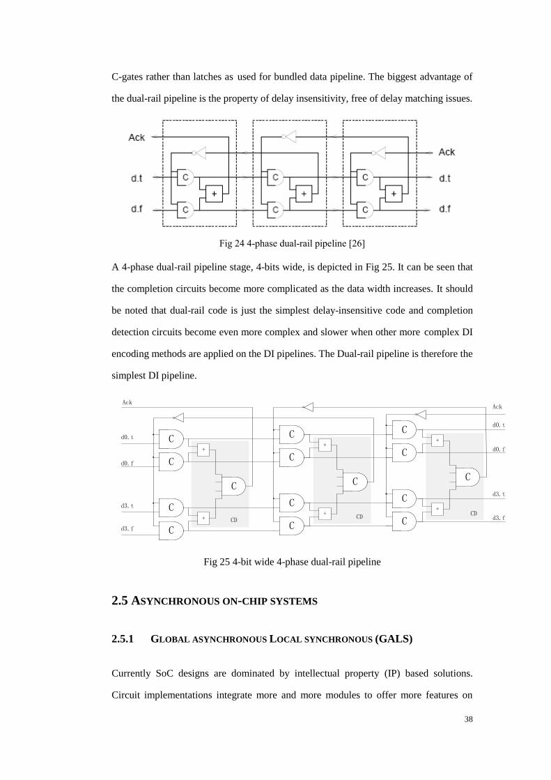
38
C-gates rather than latches as used for bundled data pipeline. The biggest advantage of
the dual-rail pipeline is the property of delay insensitivity, free of delay matching issues.
Fig 24 4-phase dual-rail pipeline [26]
A 4-phase dual-rail pipeline stage, 4-bits wide, is depicted in Fig 25. It can be seen that
the completion circuits become more complicated as the data width increases. It should
be noted that dual-rail code is just the simplest delay-insensitive code and completion
detection circuits become even more complex and slower when other more complex DI
encoding methods are applied on the DI pipelines. The Dual-rail pipeline is therefore the
simplest DI pipeline.
C
C
C
C
+
+
C
C
C
C
C
+
+
C
C
C
C
C
+
+
C
d0.t
d0.f
d3.t
d3.f
Ack
d0.t
d0.f
d3.t
d3.f
Ack
CDCD
CD
Fig 25 4-bit wide 4-phase dual-rail pipeline
2.5 ASYNCHRONOUS ON-CHIP SYSTEMS
2.5.1 GLOBAL ASYNCHRONOUS LOCAL SYNCHRONOUS (GALS)
Currently SoC designs are dominated by intellectual property (IP) based solutions.
Circuit implementations integrate more and more modules to offer more features on

39
single chips, resulting in lower cost, better power efficiency and higher performance.
Apart from meeting the market demand, the increased integration capability of advanced
VLSI technology leads to the rapidly growing complexity of SoCs. To minimize
development cycles, it is critical to reuse commercially available modules in designs. A
variety of IP modules are available in the market, such as microprocessors, memory
controllers, DSP blocks and communication processing engines. Reusing and
incorporating these silicon proven modules into a new complex SoC design can
significantly reduce the design cycle of the product. The design emphasis starts to move
from individual module designs with simple system architectures into global interconnect
designs bridging the regional computational modules, storage blocks and specific
purpose processors.
Despite the benefits of low power and low EMI, asynchronous circuits have not competed
well with their synchronous equivalents. This is because, typically, they have a lower
performance and, due to lack of CAD tool support, often take longer to design. There is
often, also, an area premium. However, partial rather than full asynchrony in circuit
design may bring benefits from asynchronous solutions to final designs. Global
asynchronous communication along with locally synchronous modules [30] was
proposed as a novel design methodology to address challenges in modern large scale SoC
designs. By contrast to fully asynchronous solutions, asynchronous network interconnect
reduces the design difficulties and, using locally synchronous modules, significantly
reduce dependency of entire designs on the required commercial tools for designing
asynchronous circuits.
An asynchronous global communication architecture, provided as intellectual property,
supplies a flexible and reliable solution to accommodate all kinds of regional blocks,
regardless of the target technology and frequency differences of the integrated modules.
Global asynchronous interconnect is a promising approach. Unlike the globally
synchronous interconnect, the timing of an asynchronous interconnect is naturally elastic.
Low power is an important design goal in modern SoCs, which demands some modules
operate at lower clock rates to save the overall power. The elastic property supports the

40
integration of these multiple clock systems without extra design effort. This approach
also eases the back-end layout as the timing closure issues for synchronous global
interconnect usually require many design iterations.
2.5.2 NETWORK ON-CHIP (NOC) AND ASYNCHRONOUS NOC
The concept of Network-on-chip is proposed [31-33] to mainly address two issues faced
in modern bus-based SoC designs: long delay and limited throughput in global
communication as the system integration increases. The trend of global wire delays as the
technology continues to shrink is shown in Fig 26. The delays incurred at local wires and
gates are scaling down, benefiting from the shrunk technology; the global wire delays
conversely become longer. Consequently the increased global wire delays necessitate
wire buffering and pipelining to improve throughput over global communication
infrastructures; the growing variance between local and global wire delays requires novel
communication architectures with better throughput than conventional on-chip buses.
Finally, highly integrated SoCs dominated by global communications lead to a growing
demand for higher communication performance. Compared to the conventional on-chip
shared bus protocols, a packet switching on-chip network is characterized by better
resistance to varied delay, more efficient wire utilization and higher parallelism [31-33].
A number of prototypes have been demonstrated, such as SPIN [31, 34], Aethereal [35],
Xpipes [36]and Nostrum [37].
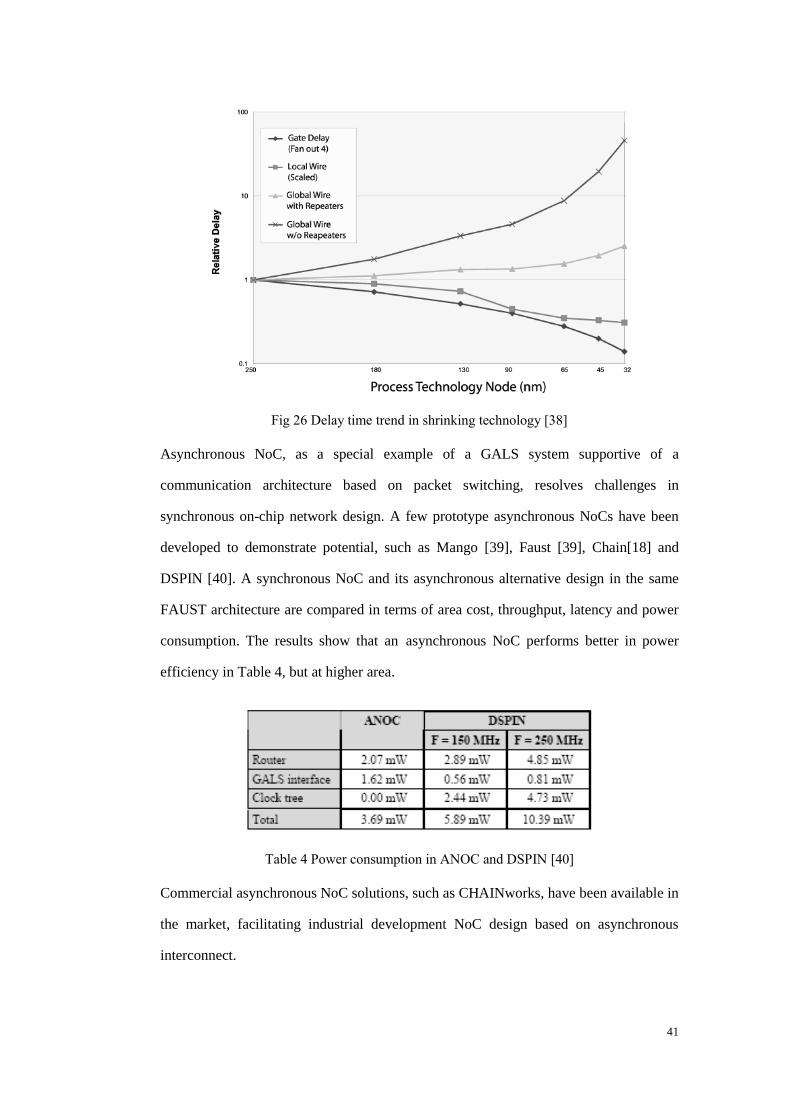
41
Fig 26 Delay time trend in shrinking technology [38]
Asynchronous NoC, as a special example of a GALS system supportive of a
communication architecture based on packet switching, resolves challenges in
synchronous on-chip network design. A few prototype asynchronous NoCs have been
developed to demonstrate potential, such as Mango [39], Faust [39], Chain[18] and
DSPIN [40]. A synchronous NoC and its asynchronous alternative design in the same
FAUST architecture are compared in terms of area cost, throughput, latency and power
consumption. The results show that an asynchronous NoC performs better in power
efficiency in Table 4, but at higher area.
Table 4 Power consumption in ANOC and DSPIN [40]
Commercial asynchronous NoC solutions, such as CHAINworks, have been available in
the market, facilitating industrial development NoC design based on asynchronous
interconnect.
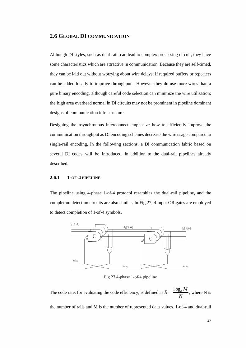
42
2.6 GLOBAL DI COMMUNICATION
Although DI styles, such as dual-rail, can lead to complex processing circuit, they have
some characteristics which are attractive in communication. Because they are self-timed,
they can be laid out without worrying about wire delays; if required buffers or repeaters
can be added locally to improve throughput. However they do use more wires than a
pure binary encoding, although careful code selection can minimize the wire utilization;
the high area overhead normal in DI circuits may not be prominent in pipeline dominant
designs of communication infrastructure.
Designing the asynchronous interconnect emphasize how to efficiently improve the
communication throughput as DI encoding schemes decrease the wire usage compared to
single-rail encoding. In the following sections, a DI communication fabric based on
several DI codes will be introduced, in addition to the dual-rail pipelines already
described.
2.6.1 1-OF-4 PIPELINE
The pipeline using 4-phase 1-of-4 protocol resembles the dual-rail pipeline, and the
completion detection circuits are also similar. In Fig 27, 4-input OR gates are employed
to detect completion of 1-of-4 symbols.
CCCC C
d0[3:0]
d2[3:0]d1[3:0]
ack1
ack2 ack3
Fig 27 4-phase 1-of-4 pipeline
The code rate, for evaluating the code efficiency, is defined asN
MR 2l og , where N is
the number of rails and M is the number of represented data values. 1-of-4 and dual-rail

43
have an equivalent code rate 0.5 in Table 5. 1-of-n codes (n>4) have lower code rates,
which means that the set of wires carries proportionately less information. Table 5 gives
an example for 8 wires, where 1-of-8 code has a code rate 3/8 and is only able to carry 3
bits of information less than 4 bits for dual-rail and 1-of-4 codes. Therefore these codes
with high rail number are rarely used in practice.
1-of-n codes Dual-rail 1-of-4 1-of-8
Information (bits) 4 4 3
Code rate 1/2 1/2 3/8
Table 5 1-of-n codes
Widening a pipeline is straightforward. Fig 28 shows a 12-bit wide pipeline is built with
multiple groups. The completion signals for each group is wired into a C-gate to generate
an acknowledge signal for each stage of the pipeline. The completion detection scheme
ensures that all data channels at a stage receive symbols before an acknowledge signal is
sent back the prior stage so that all transferred data on all channels are well ordered.
CCCC C
d0[3:0]
d2[3:0]
ack1ack2 ack3
CCCC C
d0[7:4]
d2[7:4]
CCCC C
C C
d0[11:8]
d2[11:8]
Fig 28 12 bit 1-of-4 pipeline
2.6.2 M-OF-N PIPELINE
M-of-n codes with higher code rate can be used to increase the throughput of on-chip
communication channels. In an m-of-n code, there are m „1‟s out of n wires to represent a
symbol.
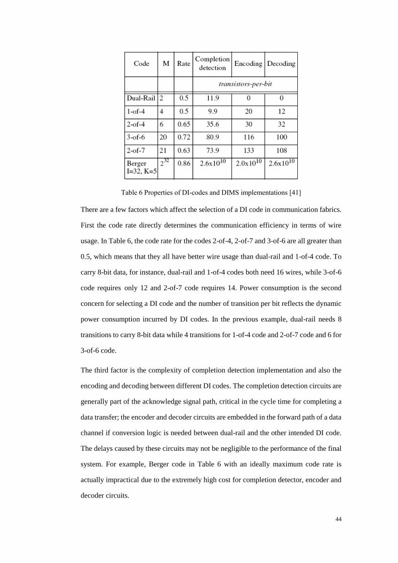
44
Table 6 Properties of DI-codes and DIMS implementations [41]
There are a few factors which affect the selection of a DI code in communication fabrics.
First the code rate directly determines the communication efficiency in terms of wire
usage. In Table 6, the code rate for the codes 2-of-4, 2-of-7 and 3-of-6 are all greater than
0.5, which means that they all have better wire usage than dual-rail and 1-of-4 code. To
carry 8-bit data, for instance, dual-rail and 1-of-4 codes both need 16 wires, while 3-of-6
code requires only 12 and 2-of-7 code requires 14. Power consumption is the second
concern for selecting a DI code and the number of transition per bit reflects the dynamic
power consumption incurred by DI codes. In the previous example, dual-rail needs 8
transitions to carry 8-bit data while 4 transitions for 1-of-4 code and 2-of-7 code and 6 for
3-of-6 code.
The third factor is the complexity of completion detection implementation and also the
encoding and decoding between different DI codes. The completion detection circuits are
generally part of the acknowledge signal path, critical in the cycle time for completing a
data transfer; the encoder and decoder circuits are embedded in the forward path of a data
channel if conversion logic is needed between dual-rail and the other intended DI code.
The delays caused by these circuits may not be negligible to the performance of the final
system. For example, Berger code in Table 6 with an ideally maximum code rate is
actually impractical due to the extremely high cost for completion detector, encoder and
decoder circuits.

45
It can be seen that the codes 2-of-7 and 3-of-6 are a reasonable compromise of all the
factors, including code efficiency and the complexity of the completion detector, encoder
and decoder, thus sensible for DI interconnect implementations. These two codes will be
described in greater detail in the chapter 4.
2.7 SUMMARY
This chapter introduced fundamental concepts in asynchronous circuit design, such as
handshake protocols and data encoding, and also some commonly used asynchronous
elements. Several 2-phase and 4-phase pipelines were discussed, along with their
respective handshake protocols. Pipelines help to shorten the response time of an
asynchronous channel and improve the throughput; thus pipelines play a important role
in on-chip global interconnect. Delay-insensitive pipelines are the most attractive
implementation due to their tolerance to unbounded delays. These concepts form the
basis of designing global DI communication.
Chapter 4 will introduce the implementation of off-chip interfaces, which are based on
on-chip DI pipelines of 4-phase 3-of-6 code while the off-chip channels use 2-phase
2-of-7 code.
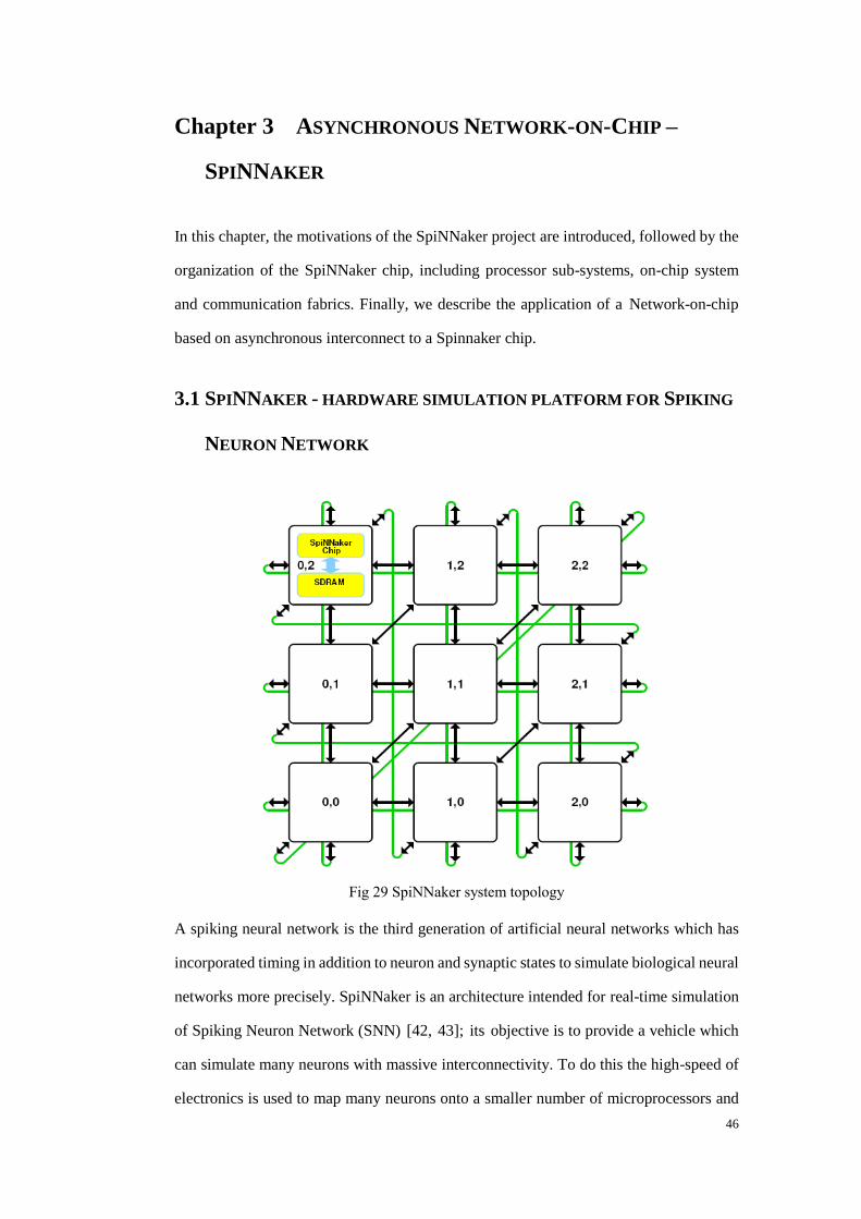
46
Chapter 3 ASYNCHRONOUS NETWORK-ON-CHIP –
SPINNAKER
In this chapter, the motivations of the SpiNNaker project are introduced, followed by the
organization of the SpiNNaker chip, including processor sub-systems, on-chip system
and communication fabrics. Finally, we describe the application of a Network-on-chip
based on asynchronous interconnect to a Spinnaker chip.
3.1 SPINNAKER - HARDWARE SIMULATION PLATFORM FOR SPIKING
NEURON NETWORK
Fig 29 SpiNNaker system topology
A spiking neural network is the third generation of artificial neural networks which has
incorporated timing in addition to neuron and synaptic states to simulate biological neural
networks more precisely. SpiNNaker is an architecture intended for real-time simulation
of Spiking Neuron Network (SNN) [42, 43]; its objective is to provide a vehicle which
can simulate many neurons with massive interconnectivity. To do this the high-speed of
electronics is used to map many neurons onto a smaller number of microprocessors and
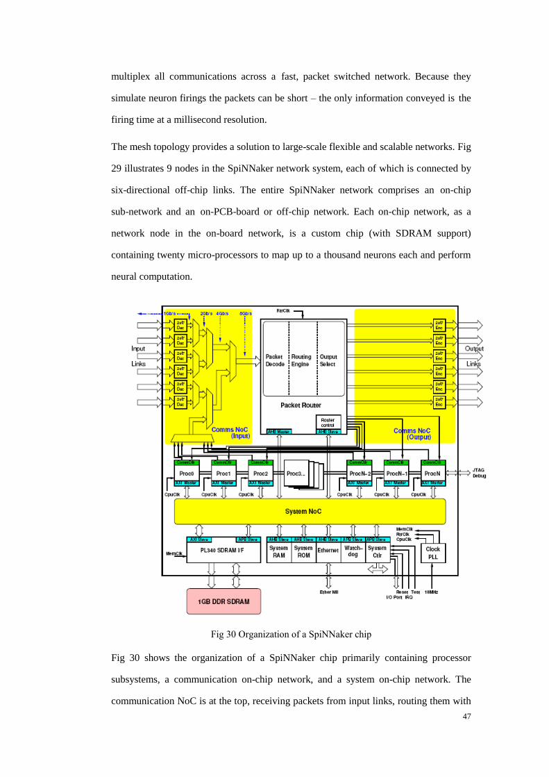
47
multiplex all communications across a fast, packet switched network. Because they
simulate neuron firings the packets can be short – the only information conveyed is the
firing time at a millisecond resolution.
The mesh topology provides a solution to large-scale flexible and scalable networks. Fig
29 illustrates 9 nodes in the SpiNNaker network system, each of which is connected by
six-directional off-chip links. The entire SpiNNaker network comprises an on-chip
sub-network and an on-PCB-board or off-chip network. Each on-chip network, as a
network node in the on-board network, is a custom chip (with SDRAM support)
containing twenty micro-processors to map up to a thousand neurons each and perform
neural computation.
Fig 30 Organization of a SpiNNaker chip
Fig 30 shows the organization of a SpiNNaker chip primarily containing processor
subsystems, a communication on-chip network, and a system on-chip network. The
communication NoC is at the top, receiving packets from input links, routing them with
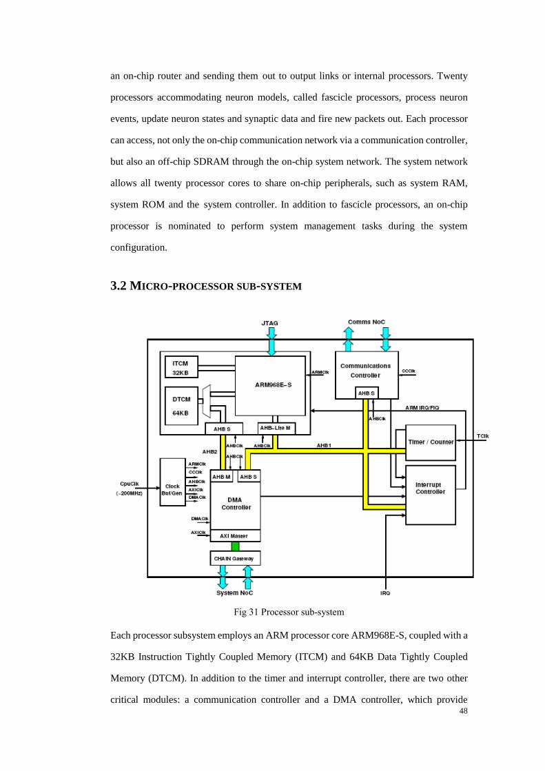
48
an on-chip router and sending them out to output links or internal processors. Twenty
processors accommodating neuron models, called fascicle processors, process neuron
events, update neuron states and synaptic data and fire new packets out. Each processor
can access, not only the on-chip communication network via a communication controller,
but also an off-chip SDRAM through the on-chip system network. The system network
allows all twenty processor cores to share on-chip peripherals, such as system RAM,
system ROM and the system controller. In addition to fascicle processors, an on-chip
processor is nominated to perform system management tasks during the system
configuration.
3.2 MICRO-PROCESSOR SUB-SYSTEM
Fig 31 Processor sub-system
Each processor subsystem employs an ARM processor core ARM968E-S, coupled with a
32KB Instruction Tightly Coupled Memory (ITCM) and 64KB Data Tightly Coupled
Memory (DTCM). In addition to the timer and interrupt controller, there are two other
critical modules: a communication controller and a DMA controller, which provide
49
accesses to the external environment as shown in Fig 31. All traffic data from or to the
Comms NoC are transferred over the bus AHB1, while the data from or to the system
NoC are carried over a dedicated bus AHB2 which provides a direct access for DTCM to
the external SDRAM.
3.3.1 DMA CONTROLLER
For each processor subsystem, there exists a demanding requirement for the
communication between the monitor or fascicle processors and the peripheral
components such as system RAM, system ROM and an off-chip SDRAM.
Communications between fascicle processors and the off-chip SDRAM occur frequently
and involve movements of large blocks of data while running an application. To improve
communication efficiency, a DMA engine alleviates the communication burden of each
processor.
Additional to the DMA operations, a bridge channel is included to provide
communication access between local processors and the peripheral components. For
instance, the monitor processor needs to access the system RAM to perform monitoring
programs; each processor reads the boot-up code from the system ROM after reset; via
the Ethernet the monitor processor downloads application program from the remote host
computer. A configurable Cyclic Redundant Check (CRC) scheme is supported to check
and even correct any corrupted data.
3.3.2 COMMUNICATION CONTROLLER
A communication controller, as an AHB device, is included in each processor node and is
responsible for transmitting and receiving packets to or from the local router.
To transmit packets, the associated processor first issues a payload into the write data
register and then configures the transmission control register via the AHB slave interface
to initiate a write DMA operation. Once the operation is finished or any exceptional state
happens, an interrupt request will be triggered to inform the processor.

50
A receiver is also incorporated in the communication controller to handle incoming
packets from the router and to pass them into a processor. The receiver unit checks parity
and framing errors for each input packet. The processor will be informed by means of
three distinct interrupts, packet received successfully, packet received with a parity errors
and packet received with a framing error.
3.3 COMMUNICATION IN MANY CORE SYSTEMS OF SPINNAKER
3.3.1 ON-CHIP SHARED BUS ARCHITECTURE
On-chip communication infrastructures have evolved rapidly to meet growing demand
due to the increase in on-chip integrated modules and system function. In this section, the
on-chip bus evolution is reviewed by taking the example of the ARM Advanced
Microcontroller Bus Architecture (AMBA) [44].
Given a simple scenario, the AHB Lite protocol is suitable for communication between a
single master and multiple slaves. The benefit is that no arbitration is required and
therefore no consequential delay penalty. When the scale of an integrated systems grows,
for instance one containing multiple masters, to handle multiple bus requests an arbiter is
needed to grant a particular master a request access to the bus. An AHB master obtaining
an “access grant” occupies the bus however and can not release the bus to other masters
until the outstanding transaction is completed some later time. In particular, for long
length bursts, the bus will not be available to any other bus masters which are queuing for
bus grants. Therefore in a system which has only a few bus masters, conventional bus
architectures offer a simple solution to meet the on-chip communication requirement. As
the number of bus masters increases, the average response time for a bus request becomes
worse.
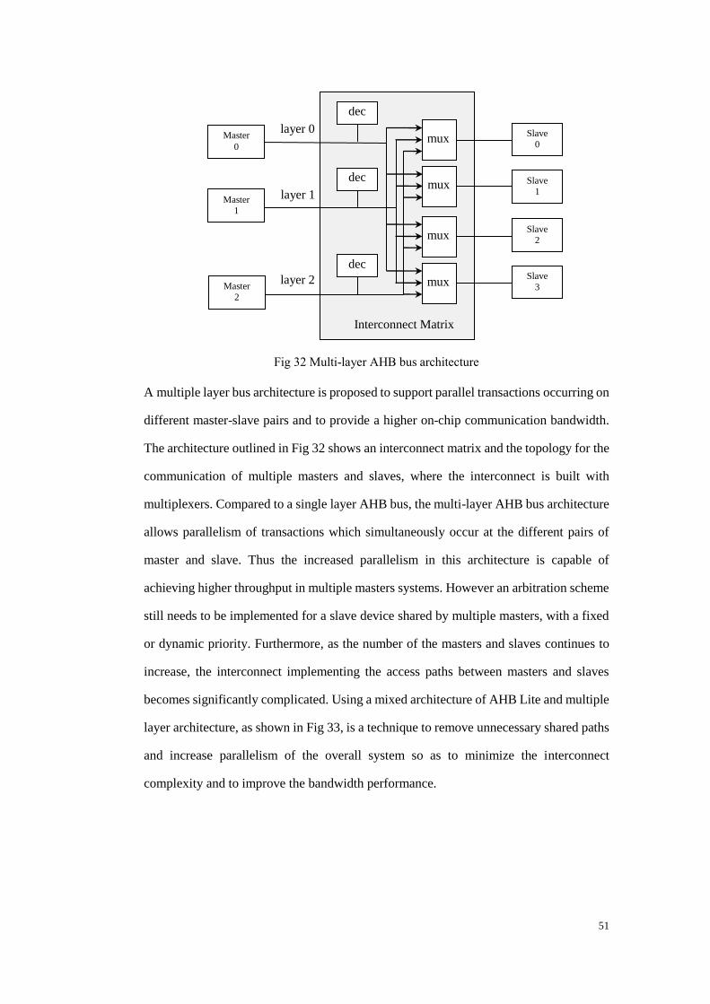
51
Fig 32 Multi-layer AHB bus architecture
A multiple layer bus architecture is proposed to support parallel transactions occurring on
different master-slave pairs and to provide a higher on-chip communication bandwidth.
The architecture outlined in Fig 32 shows an interconnect matrix and the topology for the
communication of multiple masters and slaves, where the interconnect is built with
multiplexers. Compared to a single layer AHB bus, the multi-layer AHB bus architecture
allows parallelism of transactions which simultaneously occur at the different pairs of
master and slave. Thus the increased parallelism in this architecture is capable of
achieving higher throughput in multiple masters systems. However an arbitration scheme
still needs to be implemented for a slave device shared by multiple masters, with a fixed
or dynamic priority. Furthermore, as the number of the masters and slaves continues to
increase, the interconnect implementing the access paths between masters and slaves
becomes significantly complicated. Using a mixed architecture of AHB Lite and multiple
layer architecture, as shown in Fig 33, is a technique to remove unnecessary shared paths
and increase parallelism of the overall system so as to minimize the interconnect
complexity and to improve the bandwidth performance.
mux
mux
mux
mux
Slave
0
Slave
3
Slave
1
Slave
2
dec
dec
dec
layer 0
layer 1
layer 2 Master
2
Master
0
Master
1
Interconnect Matrix
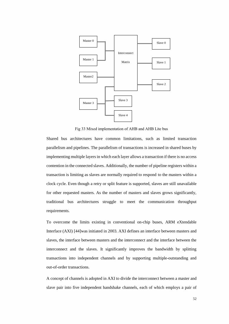
52
Fig 33 Mixed implementation of AHB and AHB Lite bus
Shared bus architectures have common limitations, such as limited transaction
parallelism and pipelines. The parallelism of transactions is increased in shared buses by
implementing multiple layers in which each layer allows a transaction if there is no access
contention in the connected slaves. Additionally, the number of pipeline registers within a
transaction is limiting as slaves are normally required to respond to the masters within a
clock cycle. Even though a retry or split feature is supported, slaves are still unavailable
for other requested masters. As the number of masters and slaves grows significantly,
traditional bus architectures struggle to meet the communication throughput
requirements.
To overcome the limits existing in conventional on-chip buses, ARM eXtendable
Interface (AXI) [44]was initiated in 2003. AXI defines an interface between masters and
slaves, the interface between masters and the interconnect and the interface between the
interconnect and the slaves. It significantly improves the bandwidth by splitting
transactions into independent channels and by supporting multiple-outstanding and
out-of-order transactions.
A concept of channels is adopted in AXI to divide the interconnect between a master and
slave pair into five independent handshake channels, each of which employs a pair of
Master 0
Master2
Master 3
Slave 4
Master 1
Slave 3
Interconnect
Matrix
Slave 0
Slave 1
Slave 2
53
handshaking signals VALID and READY. The five are write address, write data, write
response, read address and read data channels. The five independent channels split one
write transaction into three sub-transactions, write address, write data and write response,
and split one read transaction into two sub-transactions, read address and read data. Four
bit IDs have to be used to identify write and read transactions.
Decoupling the dependencies of address, data and response phases within a transaction
enable an arbitrary number of pipelines between these phases. Furthermore, these phases
as atomic sub-transactions are independent, where there is no fixed number of pipelines
required between them. For example, after receiving the read address the receiver can
send back the requested data at any time when ready. In the AHB protocol, an address
phase must be followed by a read data phase even though a few wait states can be inserted
to request more waiting cycles. Finally from an interconnect perspective, the fine grained
operations can significantly increase the interconnect utilization as the occupying time for
each transaction is effectively reduced.
The throughput of communication infrastructures can be further improved by reinforcing
access capabilities of both master and slave devices. Supporting multiple-outstanding
transactions allows a single master to initiate multiple write or read transactions,
regardless of whether earlier transactions have completed or not. If the link to a slave is
busy, a master is still able to issue transactions to access other slaves. Moreover,
out-of-order transactions allow a slave to respond to the transactions initiated by different
masters in any order regardless of their arrival order. If a slave cannot provide read data to
a master for some reason, it will not be blocked to respond to other masters with available
data.
AXI allows significantly more parallelism and pipeline stages than traditional shared
buses and significantly increases the utilization of interconnect so as to improve the
throughput in a complex on-chip communication system. Additionally it also reduces the
integration difficulty of a large number of devices by providing a flexible interconnect.
Therefore, in a SpiNNaker system AXI is employed to maximally provide access for
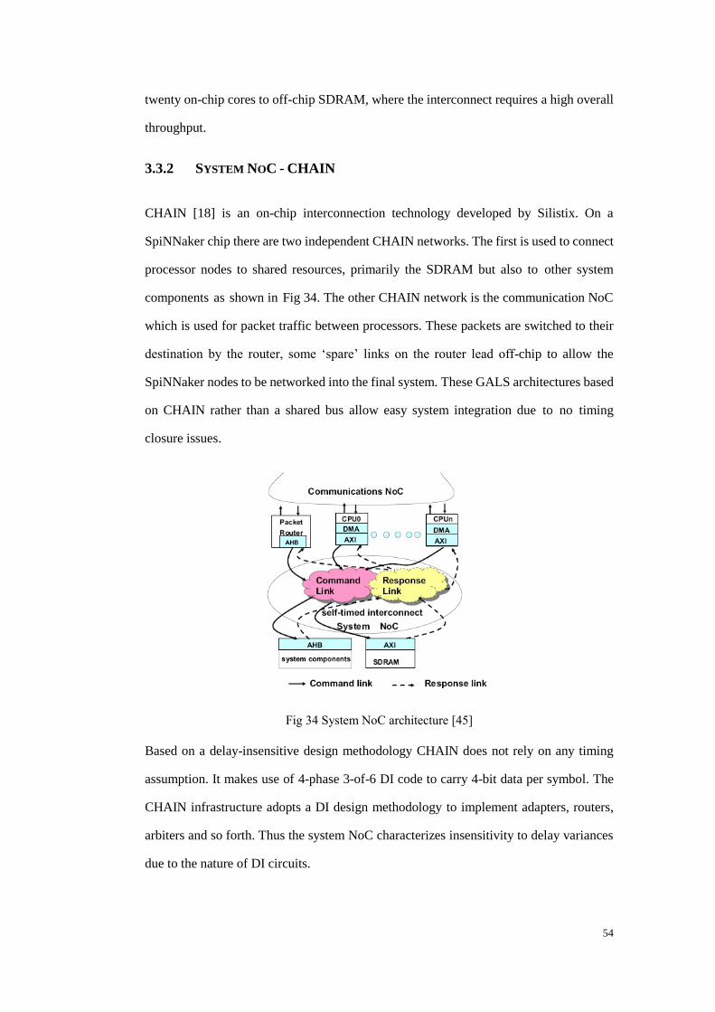
54
twenty on-chip cores to off-chip SDRAM, where the interconnect requires a high overall
throughput.
3.3.2 SYSTEM NOC - CHAIN
CHAIN [18] is an on-chip interconnection technology developed by Silistix. On a
SpiNNaker chip there are two independent CHAIN networks. The first is used to connect
processor nodes to shared resources, primarily the SDRAM but also to other system
components as shown in Fig 34. The other CHAIN network is the communication NoC
which is used for packet traffic between processors. These packets are switched to their
destination by the router, some „spare‟ links on the router lead off-chip to allow the
SpiNNaker nodes to be networked into the final system. These GALS architectures based
on CHAIN rather than a shared bus allow easy system integration due to no timing
closure issues.
Fig 34 System NoC architecture [45]
Based on a delay-insensitive design methodology CHAIN does not rely on any timing
assumption. It makes use of 4-phase 3-of-6 DI code to carry 4-bit data per symbol. The
CHAIN infrastructure adopts a DI design methodology to implement adapters, routers,
arbiters and so forth. Thus the system NoC characterizes insensitivity to delay variances
due to the nature of DI circuits.
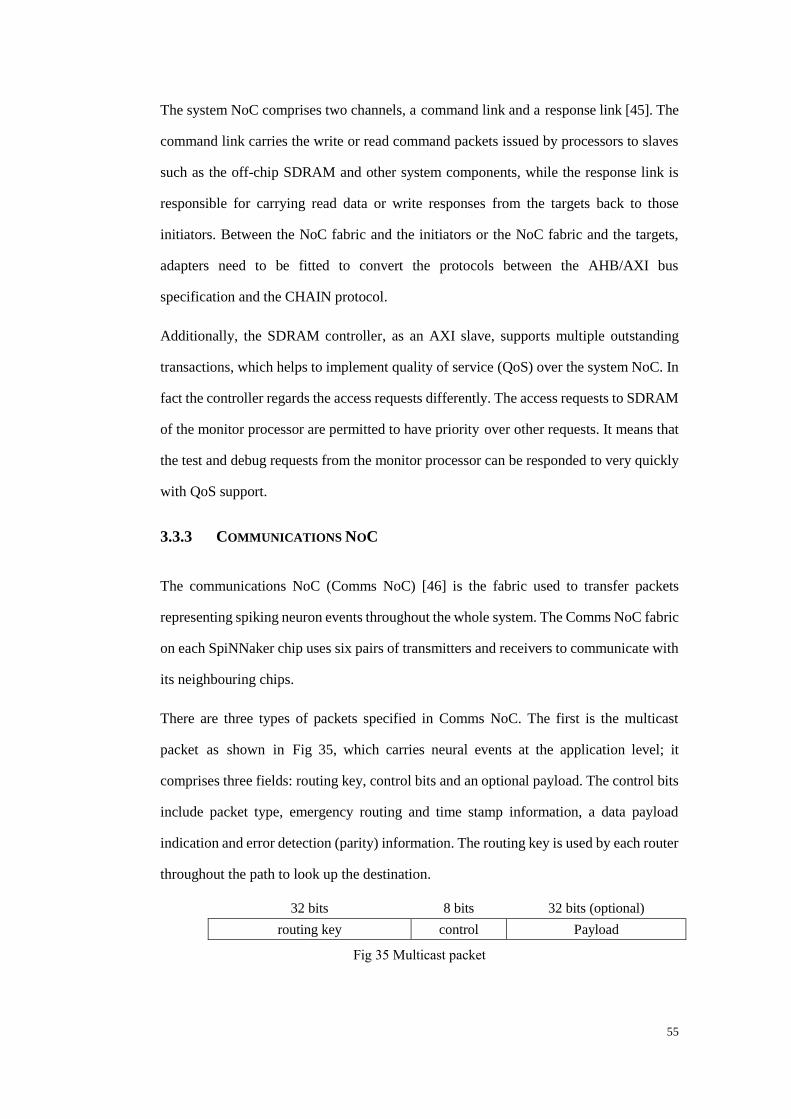
55
The system NoC comprises two channels, a command link and a response link [45]. The
command link carries the write or read command packets issued by processors to slaves
such as the off-chip SDRAM and other system components, while the response link is
responsible for carrying read data or write responses from the targets back to those
initiators. Between the NoC fabric and the initiators or the NoC fabric and the targets,
adapters need to be fitted to convert the protocols between the AHB/AXI bus
specification and the CHAIN protocol.
Additionally, the SDRAM controller, as an AXI slave, supports multiple outstanding
transactions, which helps to implement quality of service (QoS) over the system NoC. In
fact the controller regards the access requests differently. The access requests to SDRAM
of the monitor processor are permitted to have priority over other requests. It means that
the test and debug requests from the monitor processor can be responded to very quickly
with QoS support.
3.3.3 COMMUNICATIONS NOC
The communications NoC (Comms NoC) [46] is the fabric used to transfer packets
representing spiking neuron events throughout the whole system. The Comms NoC fabric
on each SpiNNaker chip uses six pairs of transmitters and receivers to communicate with
its neighbouring chips.
There are three types of packets specified in Comms NoC. The first is the multicast
packet as shown in Fig 35, which carries neural events at the application level; it
comprises three fields: routing key, control bits and an optional payload. The control bits
include packet type, emergency routing and time stamp information, a data payload
indication and error detection (parity) information. The routing key is used by each router
throughout the path to look up the destination.
32 bits 8 bits 32 bits (optional)
routing key control Payload
Fig 35 Multicast packet
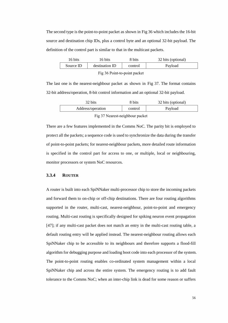
56
The second type is the point-to-point packet as shown in Fig 36 which includes the 16-bit
source and destination chip IDs, plus a control byte and an optional 32-bit payload. The
definition of the control part is similar to that in the multicast packets.
16 bits 16 bits 8 bits 32 bits (optional)
Source ID destination ID control Payload
Fig 36 Point-to-point packet
The last one is the nearest-neighbour packet as shown in Fig 37. The format contains
32-bit address/operation, 8-bit control information and an optional 32-bit payload.
32 bits 8 bits 32 bits (optional)
Address/operation control Payload
Fig 37 Nearest-neighbour packet
There are a few features implemented in the Comms NoC. The parity bit is employed to
protect all the packets; a sequence code is used to synchronize the data during the transfer
of point-to-point packets; for nearest-neighbour packets, more detailed route information
is specified in the control part for access to one, or multiple, local or neighbouring,
monitor processors or system NoC resources.
3.3.4 ROUTER
A router is built into each SpiNNaker multi-processor chip to store the incoming packets
and forward them to on-chip or off-chip destinations. There are four routing algorithms
supported in the router, multi-cast, nearest-neighbour, point-to-point and emergency
routing. Multi-cast routing is specifically designed for spiking neuron event propagation
[47]; if any multi-cast packet does not match an entry in the multi-cast routing table, a
default routing entry will be applied instead. The nearest-neighbour routing allows each
SpiNNaker chip to be accessible to its neighbours and therefore supports a flood-fill
algorithm for debugging purpose and loading boot code into each processor of the system.
The point-to-point routing enables co-ordinated system management within a local
SpiNNaker chip and across the entire system. The emergency routing is to add fault
tolerance to the Comms NoC; when an inter-chip link is dead for some reason or suffers
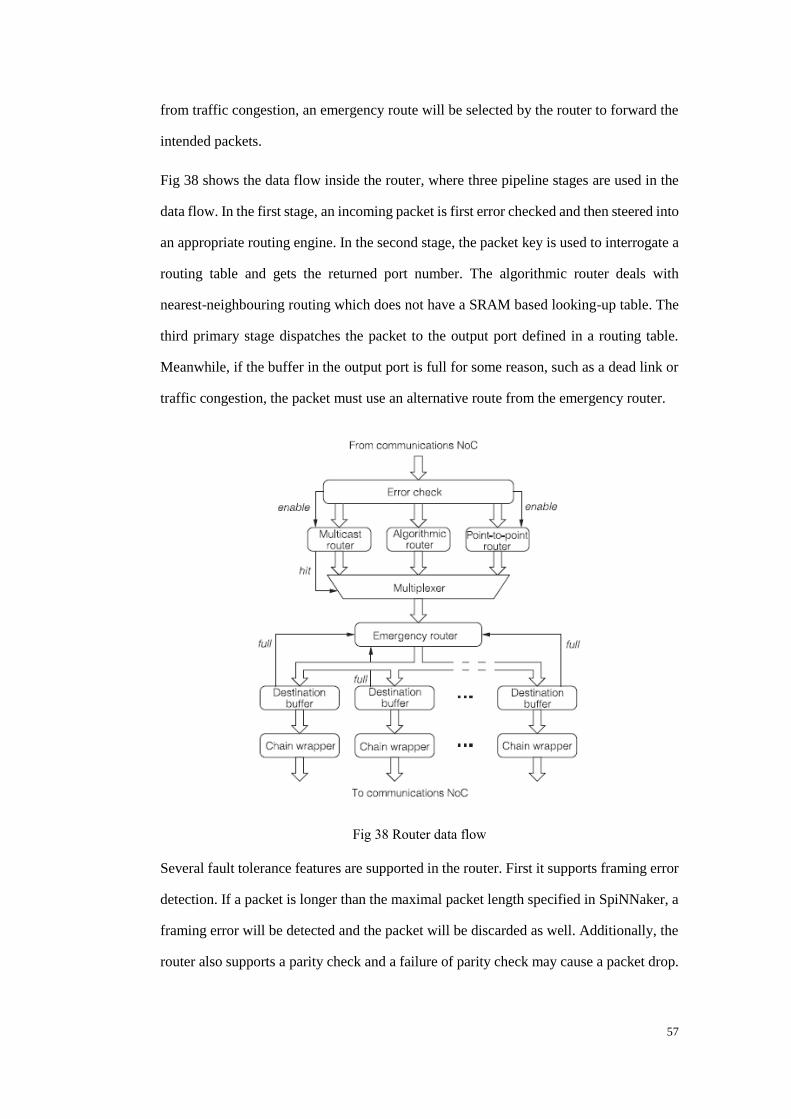
57
from traffic congestion, an emergency route will be selected by the router to forward the
intended packets.
Fig 38 shows the data flow inside the router, where three pipeline stages are used in the
data flow. In the first stage, an incoming packet is first error checked and then steered into
an appropriate routing engine. In the second stage, the packet key is used to interrogate a
routing table and gets the returned port number. The algorithmic router deals with
nearest-neighbouring routing which does not have a SRAM based looking-up table. The
third primary stage dispatches the packet to the output port defined in a routing table.
Meanwhile, if the buffer in the output port is full for some reason, such as a dead link or
traffic congestion, the packet must use an alternative route from the emergency router.
Fig 38 Router data flow
Several fault tolerance features are supported in the router. First it supports framing error
detection. If a packet is longer than the maximal packet length specified in SpiNNaker, a
framing error will be detected and the packet will be discarded as well. Additionally, the
router also supports a parity check and a failure of parity check may cause a packet drop.
58
Finally, to avoid backlog in on-chip communication, the router has adequate space to
buffer a whole packet and then process.
3.3.5 INPUT AND OUTPUT SECTIONS
The input and output sections, connected to the router inside a multi-processor node,
bridge asynchronous and synchronous domains and complete code conversion and
serialization/de-serialization across the entire SpiNNaker system [46]. The input section
receives packets from either off-chip links or on-chip fascicle processors and passes them
on to the router, while the output section simply includes serializers to pass data to
off-chip links or to on-chip fascicle processor via communication controllers.
The challenge in the input sections is the increasing bandwidth requirement which results
from multiple input data flows for each chip node including six off-chip links and roughly
twenty on-chip links to all the fascicle processors. To prevent the input section from
introducing extra delay through the link, 2-way mergers and bandwidth aggregator (BA)
units are used in the input section. Each buffer-based BA guarantees that the output
bandwidth is twice its input bandwidth. The buffer-based BA is implemented by making
the CHAIN link number of its output twice than that of its input. Additionally, each router
works at 200 MHz and normally within one clock cycle latency can process an incoming
packet 40 or 72 bits wide. Routers operate quickly enough to catch up with the transfer
bandwidth of each link. A tree of three levels of BAs and mergers can provide an input
data flow into the router with a bandwidth eight times greater than that of an off-chip link
and thus each link between two chip nodes can carry data at their maximum rate without
the congestion caused by low on-chip receiving rate.
3.3.6 OFF-CHIP NETWORKING
In principle it is possible to extend CHAIN links between chips; they are DI and therefore
can simply be connected and will function. However there are other constraints:
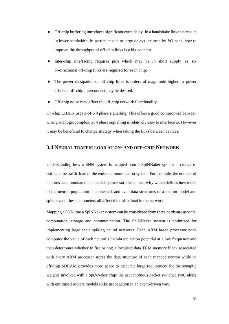
59
Off-chip buffering introduces significant extra delay. In a handshake link this results
in lower bandwidth; in particular due to large delays incurred by I/O pads, how to
improve the throughput of off-chip links is a big concern.
Inter-chip interfacing requires pins which may be in short supply as six
bi-directional off-chip links are required for each chip;
The power dissipation of off-chip links is orders of magnitude higher; a power
efficient off-chip interconnect may be desired.
Off-chip noise may affect the off-chip network functionality.
On-chip CHAIN uses 3-of-6 4 phase signalling. This offers a good compromise between
wiring and logic complexity; 4 phase signalling is relatively easy to interface to. However
it may be beneficial to change strategy when taking the links between devices.
3.4 NEURAL TRAFFIC LOAD AT ON- AND OFF-CHIP NETWORK
Understanding how a SNN system is mapped onto a SpiNNaker system is crucial to
estimate the traffic load of the entire communication system. For example, the number of
neurons accommodated in a fascicle processor, the connectivity which defines how much
of the neuron population is connected, and even data structures of a neuron model and
spike event, these parameters all affect the traffic load in the network.
Mapping a SNN into a SpiNNaker system can be considered from three hardware aspects:
computation, storage and communication. The SpiNNaker system is optimized for
implementing large scale spiking neural networks. Each ARM based processor node
computes the value of each neuron‟s membrane action potential at a low frequency and
then determines whether to fire or not; a localised data TCM memory block associated
with every ARM processor stores the data structure of each mapped neuron while an
off-chip SDRAM provides more space to meet the large requirement for the synaptic
weights involved with a SpiNNaker chip; the asynchronous packet switched NoC along
with optimised routers models spike propagation in an event-driven way.

60
As a case study [48], the Izhikevich model [49] was implemented on the SpiNNaker
system for the well balanced compromise of computational efficiency and functional
richness. From the computational point of view, the hardware simulating a neuron has to
handle three primary tasks: extracting synaptic weights, accumulating current for each
stimulus and updating the neuron state to fire spikes if the membrane potential reaches
the firing threshold. Though the SpiNNaker hardware is transparent to the application
level, accomplishing the three tasks through the SpiNNaker architecture, it is optimized
to support the spiking neural network application. In detail, the input packets representing
neural spikes are routed off chip or to local fascicle processors through the multi-cast
routers and communication controllers; these packets, representing the neuron stimulus,
are passed and stored in the DTCM. The application running in a processor retrieves a
few parameters from the DTCM, including the synaptic delay, the ID of the source
fascicle processor and the ID of the pre-synaptic neuron.
Each fascicle processor can accommodate around one thousand neurons, representing the
neuron‟s state using a fixed point format instead of floating point format as the ARM
processors do not include floating point units. 16-bit precision fixed point is employed
with a reasonable hardware cost to maximally approximate to the original Izhikevich
Model implemented with the support of floating point. A data structure defining all the
variables in a neuron model is specified to store its state in the local DTCM.
In addition to the data structure, there is a storage requirement associated with the large
number of connected other neurons in which synaptic weights are used to define the
connection strength. Assuming one processor accommodates one thousand neurons, the
memory demand for storing synaptic weights would be tens of Mega bytes which is far
beyond the size of a local DTCM. Thus an off-chip SDRAM of relatively large volume is
necessary to provide space for synaptic weights. However it should be noted that the
access requirement for the SDRAM is not a significant issue due to the low firing
frequency of each neuron.
The case study shows that the SpiNNaker hardware is capable of supporting the
application of a spiking neural network based on the Izhikevich model. Once a spike has
61
travelled from a pre-synaptic neuron to a given fascicle processor, the communication
controller passes the IDs of the processor and the pre-synaptic neuron where the spike
starts from to the destination fascicle processor in an interrupt mode. A look-up table is
built into the fascicle processor to provide the address in the off-chip SDRAM, at which
all the synaptic weights of the connections with the pre-synaptic neuron are located. As
far as a post-synaptic neuron is concerned, a synaptic weight corresponding to every input
spike is then obtained from the SDRAM through a DMA operation and accumulated to
the neuron stimulus current by the processor. The neuron simulation then decides whether
to fire a spike by calculating its state in the Izhikevich model.
Fig 39 Modelling neuron propagation delay [50]
Another issue is how to model the biological delays taken to propagate spikes over axons
and synapses in hardware. Compared to the millisecond scale of the biological axonal
delays, the propagation time of an on-chip communication channel is actually trivial,
generally less than 1us. To model the real axonal delay, a special 4bit field is specified in
the spike packets [48], ranging from 1ms to 16ms. However the destination fascicle
processor must be capable of distinguishing these simulated axonal delays and treat the
spikes differently. A 16 entry circular array is built for 16 delays; spikes with different
delays add their synaptic weights to the appropriate delay bins in Fig 39. The last task
updating neurons‟ states is not initiated immediately once packets arrive; instead each
neuron‟s state is updated at a frequency of the real neurons firing. The accumulated
current for all input stimuli, really arriving at the current simulation time, are passed
along with the previous state parameters to the two Izhikevich equations. The
62
computation result will determine if the neuron fires a spike to its output port. The Global
communication infrastructure in SpiNNaker can provide an approximate simulation to a
spiking neural network based on the Izhikevich model. However, it is quite difficult for a
hardware system to produce exactly the same model as the biological neural system.
More discussions would be beyond the scope of this thesis.
The required throughput for the DMA channel via the system NoC depends on the
number of pre-synaptic neurons which are connected to all the neurons in a given
SpiNNaker chip. For example, each neuron in a fascicle processor may have on average
1000 connections with pre-synaptic neurons, all the neurons fire at 10Hz and 16 fascicle
processors work in a chip; hence the throughput for its off-chip SDRAM is 1000 Neurons
x 1000 connections x 10Hz x 16 processors x 2Bytes = 320 MB/s. In the SpiNNaker
system, the associated off-chip SDRAMs have more than 1GB/s bandwidth each, which
has a potential to support more than 100 dendrite connections per neuron.
A pre-synaptic neuron may be connected to a number of other neurons within a fascicle
processor. This does not help to decrease the required throughput of access to SDRAMs,
but it indicates that the throughput requirement for the on-chip Comms NoC is reduced
significantly. Based on the previous calculation, similarly we have a rough estimation of
traffic load at on-chip Comms NoC, 1000Neurons x 100connections x 100Hz = 10M/s,
around 10M spikes for each fascicle processor, namely 40M Bytes per second assuming 4
Bytes for each spike packet payload. If a pre-synaptic neuron is connected to 10
post-synaptic neurons, the total traffic load for a fascicle processor is reduced to 4M
Bytes per second. We can estimate the outgoing spike packets, 1000Neurons x
10connections x 100Hz x 8Bytes = 8MB/s. Thus each fascicle processor has to process all
incoming and outgoing packets: 4+8=12MB/s, which also is the work load for each
associated communication controller.
Finally, we need to look at the traffic load for each SpiNNaker chip, particularly for the
embedded router. Assuming N chip nodes are implemented in the entire system network,
the total generated packets of the system is N nodes x 16 processors x 1000 neurons x
100Hz x 8Bytes = N x 12.8 MB/s. We need to make an assumption on the average

63
number of hops for spike packets. Given a 100x100 network which can accommodate up
to 160 million neurons, we take 50 as the average number of hops. So the total spike
packets in the entire network would be N x 12.8 x 50 =N x 640 MB/s. The traffic load for
each node is 640 MB/s; each bidirectional inter-chip link would have 640/6=107MB/s.
Given the network example of a 100x100 scale with 100 dendrite connections and 10
axonal connections, the analysis of traffic loads shows that SpiNNaker system can meet
the throughput requirement for SDRAM, on-chip communication.
This case study, however, has not incorporated any learning rule to update synaptic
weights, which means that the synaptic weights stored in the off-chip SDRAM are
constant without any modification for learning. If applying a learning rule, write-back
operations are required to modify the synaptic weights in the SDRAMs and the
throughput requirement for SDRAM will be increased accordingly. The SpiNNaker
system is still able to implement a complex application implementing a learning
algorithm.
3.5 FAULT TOLERANCE REQUIREMENTS IN SPINNAKER
As a large scale real-time spiking neuron simulation system, a SpiNNaker system not
only supports the integration of many cores in a chip but also can be easily extended to
integrate hundreds of SpiNNaker chips, where a large amount of SRAMs and
communication infrastructure are incorporated. In such a large scale system, a
malfunction in any module is rather difficult to identify and may lead to a serious issue in
the application if the system does not support appropriate fault tolerance.
Thus it is essential to examine the impacts of transient or permanent faults in every part of
the system and then come up with effective fault tolerant techniques to enhance the
robustness of the entire system at the different levels. From the hardware point of view,
on-chip processors, SRAM blocks, communication fabrics and routers are the key
hardware modules which require fault tolerant techniques to ensure correct operations in
the application.
64
Some processor nodes, for instance, may fail in the self-test programs during set-up or
while performing application program at run time due to manufacturing defects or
intermittent faults or even transient glitches. The system monitors need a scheme to
identify the faulty processors or nodes and allocate spare ones to take over their
application functions. One benefit of this scheme is to minimize the interference of faulty
hardware to other functional hardware. The traffic generated by faulty processors, for
instance, unnecessarily increases the workload of the communication infrastructure and
may considerably cause negative influence on the spiking neural network application.
The fault isolation and resource re-allocation scheme make the faulty hardware invisible
to the application and significantly reduce the fault tolerance requirement for the
application system.
Besides micro-processors, on-chip SRAMs are another example of critical hardware
which needs fault tolerant techniques. The ARM968 Processors used in SpiNNaker have
already incorporated an Error Checking and Correcting (ECC) supportive interface to the
Tightly Coupled Memory (TCM). An ECC code, such as Cyclic Redundancy Check
(CRC) or Reed-Solomon Code, can be easily implemented to greatly reduce the influence
of transient errors on the program and data memory of the on-chip processors. Moreover,
off-chip SDRAMs also need fault tolerance schemes to protect their data content, as these
store the synaptic weights and neuron states. Finally, in a large scale network the
topology and routing protocol are also objectives of investigating their fault tolerance to
faults.
Global on-chip communication fabric plays a key role in the SpiNNaker system. Faults
occurring in routers or on- or off-chip links may have a significant impact on the
application. It is critical to provide sufficient fault resistance to identity and isolate faulty
data or hardware modules. A router contains a large volume of SRAM to build their
routing tables. Tolerance for both permanent and transient faults is desired. If failing to
pass the memory tests, for example, a router probably needs to be isolated from the
hardware system. Default routing is supported if a packet does not match any routing
entry. Additionally, to protect the contents of the packets carrying neuron spikes, parity
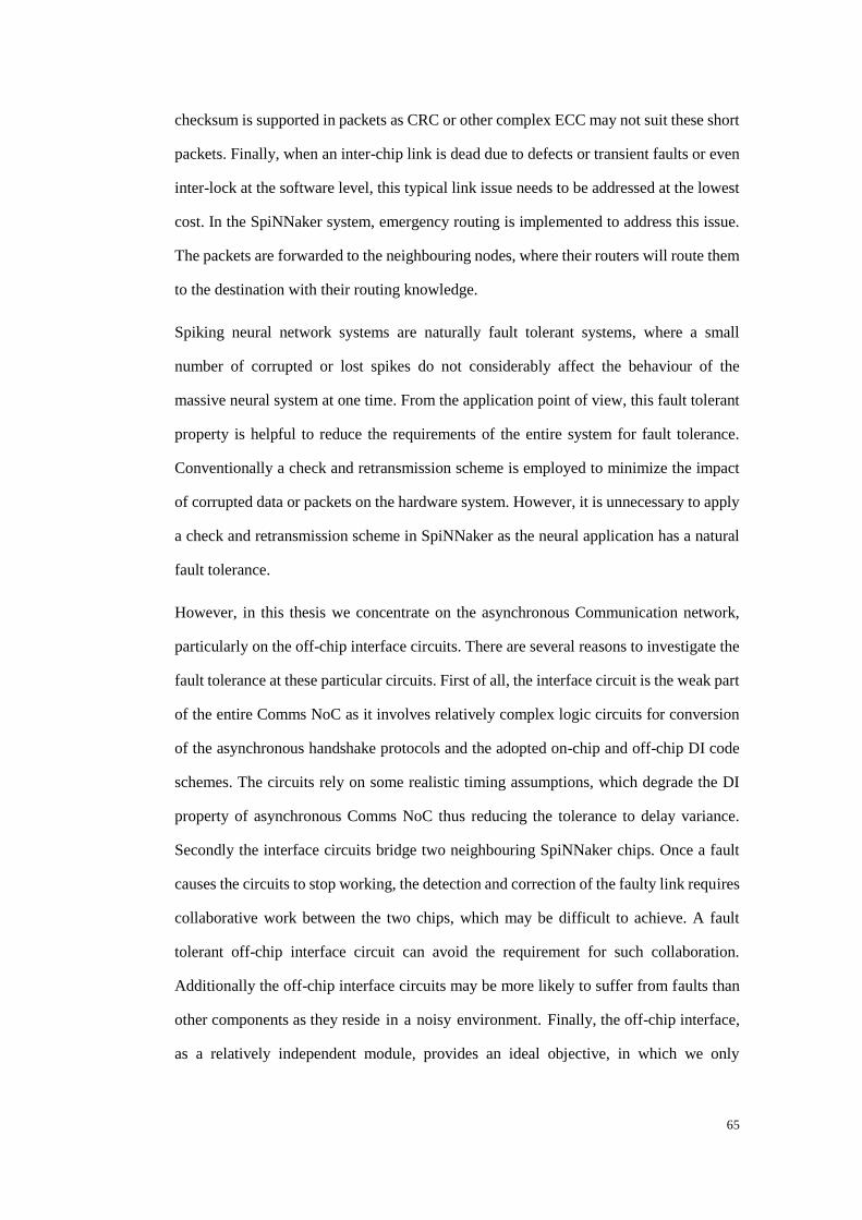
65
checksum is supported in packets as CRC or other complex ECC may not suit these short
packets. Finally, when an inter-chip link is dead due to defects or transient faults or even
inter-lock at the software level, this typical link issue needs to be addressed at the lowest
cost. In the SpiNNaker system, emergency routing is implemented to address this issue.
The packets are forwarded to the neighbouring nodes, where their routers will route them
to the destination with their routing knowledge.
Spiking neural network systems are naturally fault tolerant systems, where a small
number of corrupted or lost spikes do not considerably affect the behaviour of the
massive neural system at one time. From the application point of view, this fault tolerant
property is helpful to reduce the requirements of the entire system for fault tolerance.
Conventionally a check and retransmission scheme is employed to minimize the impact
of corrupted data or packets on the hardware system. However, it is unnecessary to apply
a check and retransmission scheme in SpiNNaker as the neural application has a natural
fault tolerance.
However, in this thesis we concentrate on the asynchronous Communication network,
particularly on the off-chip interface circuits. There are several reasons to investigate the
fault tolerance at these particular circuits. First of all, the interface circuit is the weak part
of the entire Comms NoC as it involves relatively complex logic circuits for conversion
of the asynchronous handshake protocols and the adopted on-chip and off-chip DI code
schemes. The circuits rely on some realistic timing assumptions, which degrade the DI
property of asynchronous Comms NoC thus reducing the tolerance to delay variance.
Secondly the interface circuits bridge two neighbouring SpiNNaker chips. Once a fault
causes the circuits to stop working, the detection and correction of the faulty link requires
collaborative work between the two chips, which may be difficult to achieve. A fault
tolerant off-chip interface circuit can avoid the requirement for such collaboration.
Additionally the off-chip interface circuits may be more likely to suffer from faults than
other components as they reside in a noisy environment. Finally, the off-chip interface,
as a relatively independent module, provides an ideal objective, in which we only
66
consider the transient glitches occurring on off-chip wires for fault tolerance
investigation.
3.6 SUMMARY
In this chapter, we introduced the SpiNNaker project from the hardware system‟s view,
including microprocessor sub-ystems and two types of on-chip network, the
communication NoC and the system NoC. In the communication NoC, delay-insensitive
interconnects are employed in SpiNNaker systems to convey neuron spikes within a
single chip or across chips. To improve the on-chip communication performance,
asynchronous communication systems are used to connect all locally-synchronous
modules, such as routers and microprocessors. Additionally, the traffic load was
analyzed to demonstrate that the target hardware system can meet the application
requirements. Finally, the demands for resistance against transient faults in SpiNNaker
were discussed.
The implementation of off-chip interfaces in the communication NoC is given in the
next chapter.
67
Chapter 4 ASYNCHRONOUS INTERCONNECT
IMPLEMENTATION IN SPINNAKER
This chapter describes the off-chip interconnect for SpiNNaker, omitting the fault
tolerance features, which are included in the subsequent chapter. Initial designs for the
transmitter and receiver are given; these form the baseline for the later designs which will
tolerate glitches on the off-chip wires.
4.1 OVERVIEW
The communication infrastructure comprises two parts: on-chip 4-phase or
Return-To-Zero (RTZ) asynchronous interconnects and off-chip 2-phase or
Non-Return-to-Zero (NRZ) interconnects as shown in Fig 40.
TX RX2-of-7 NRZ
3-of-6 RTZ3-of-6 RTZ
Fig 40 An off-chip link
The first part to address is the pin restriction; there are six off-chip links on each
SpiNNaker chip, each comprising two uni-directional channels. Thus saving a single wire
in a channel reduces the pin count by 12.
The on-chip communication link transmits symbols via a 3-of-6 code with an
accompanying 1-of-3 control channel, where a symbol carried on on- and off-chip links
is a packet flit. Each of those has an independent acknowledgement, thus there are
6+1+3+1=11 wires per channel. These carry 4 bit of information per cycle. In principle a
3-of-6 link can indicate 20 different symbols but some are not used which simplifies the
encode/decode logic. The added parallel information adds one more flit – one of the
1-of-3 codes is unused in SpiNNaker - indicating whether a flit is the last in a particular
packet. In practice, most flits are not EoP but NORMAL symbols which indicate all flits
68
other than the last. The third one is „Padding‟ which is not used in the communication
NoC but is used in the system NoC to indicate non-data flits between normal packets.
Off-chip information is recoded into a single 2-of-7 code which is capable of carrying up
to 21 different symbols. Because this is fewer than the on-chip code capacity which
supports up to 20x2 (20 CHAIN data symbols and 2 CHAIN control symbols) a
compromise is made where an explicit EoP marker is sent as an extra flit. EoPs are „rare‟;
a packet is 40 or 72 bits (10 or 18 flits) so the overhead in terms of cycles is ~10%. Thus
17 of the 21 2-of-7 symbols are employed. Table 7 shows the chosen encodings. Each
off-chip channel therefore uses 8 pins (including its acknowledgement) a saving of two
per channel (neglecting one unused control wire) or saving 24 pins per chip.
The second concern on the interface circuit is the power efficiency and off-chip
communication performance. To increase the power efficiency and throughput of the
communication links, the off-chip interconnect employs the 2-phase asynchronous
protocol as this reduces the number of transitions, saving half of the power consumed by
the RTZ protocol and incurring only half the round-trip cycle delays per symbol.
However, due to the higher complexity of pipelines based on the NRZ protocol, the
on-chip interconnect uses the 4-phase protocol. Moreover, a 3-of-6 encoding is used for
on-chip interconnects and a 2-of-7 code for off-chip interconnects. The two codes are
both capable of transferring 4-bits of data per symbol, with the 3-of-6 code needing one
fewer wire and the 2-of-7 code one fewer transition per symbol.
Admittedly, if the off-chip channels use the same 3-of-6 code a further saving of 12 pins
can be achieved for each chip. However, a 2-of-7 code applied to the off-chip channel
reduces the power consumed by inter-chip communication by 1/3. From the system point
of view, this is a sensible trade-off to achieve higher power-efficiency while 24 pins are
saved by removing on-chip control channels, at the cost of more design complexity. No
research has so far been found on the fault tolerance of similar circuits for converting
between 2-phase and 4-phase protocols. Thus the work described in this thesis may
arouse interest in this type of asynchronous circuit.
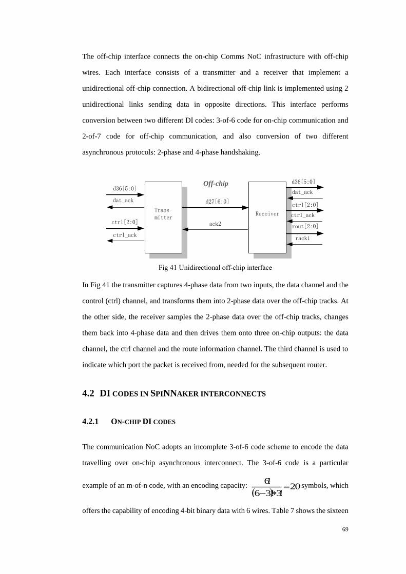
69
The off-chip interface connects the on-chip Comms NoC infrastructure with off-chip
wires. Each interface consists of a transmitter and a receiver that implement a
unidirectional off-chip connection. A bidirectional off-chip link is implemented using 2
unidirectional links sending data in opposite directions. This interface performs
conversion between two different DI codes: 3-of-6 code for on-chip communication and
2-of-7 code for off-chip communication, and also conversion of two different
asynchronous protocols: 2-phase and 4-phase handshaking.
Trans-mitter
d27[6:0]
d36[5:0]
dat_ack
ack2
Receiver
ctrl[2:0]
ctrl_ack
Off-chip d36[5:0]
dat_ack
ctrl[2:0]
ctrl_ack
rout[2:0]
racki
Fig 41 Unidirectional off-chip interface
In Fig 41 the transmitter captures 4-phase data from two inputs, the data channel and the
control (ctrl) channel, and transforms them into 2-phase data over the off-chip tracks. At
the other side, the receiver samples the 2-phase data over the off-chip tracks, changes
them back into 4-phase data and then drives them onto three on-chip outputs: the data
channel, the ctrl channel and the route information channel. The third channel is used to
indicate which port the packet is received from, needed for the subsequent router.
4.2 DI CODES IN SPINNAKER INTERCONNECTS
4.2.1 ON-CHIP DI CODES
The communication NoC adopts an incomplete 3-of-6 code scheme to encode the data
travelling over on-chip asynchronous interconnect. The 3-of-6 code is a particular
example of an m-of-n code, with an encoding capacity:
20!3!36
!6
symbols, which
offers the capability of encoding 4-bit binary data with 6 wires. Table 7 shows the sixteen
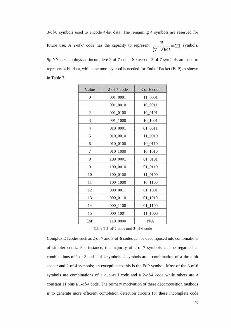
70
3-of-6 symbols used to encode 4-bit data. The remaining 4 symbols are reserved for
future use. A 2-of-7 code has the capacity to represent
21!2!27
!7
symbols.
SpiNNaker employs an incomplete 2-of-7 code. Sixteen of 2-of-7 symbols are used to
represent 4-bit data, while one more symbol is needed for End of Packet (EoP) as shown
in Table 7.
Value 2-of-7 code 3-of-6 code
0 001_0001 11_0001
1 001_0010 10_0011
2 001_0100 10_0101
3 001_1000 10_1001
4 010_0001 01_0011
5 010_0010 11_0010
6 010_0100 10_0110
7 010_1000 10_1010
8 100_0001 01_0101
9 100_0010 01_0110
10 100_0100 11_0100
11 100_1000 10_1100
12 000_0011 01_1001
13 000_0110 01_1010
14 000_1100 01_1100
15 000_1001 11_1000
EoP 110_0000 N/A
Table 7 2-of-7 code and 3-of-6 code
Complex DI codes such as 2-of-7 and 3-of-6 codes can be decomposed into combinations
of simpler codes. For instance, the majority of 2-of-7 symbols can be regarded as
combinations of 1-of-3 and 1-of-4 symbols. 4 symbols are a combination of a three-bit
spacer and 2-of-4 symbols; an exception to this is the EoP symbol. Most of the 3-of-6
symbols are combinations of a dual-rail code and a 2-of-4 code while others are a
constant 11 plus a 1-of-4 code. The primary motivation of these decomposition methods
is to generate more efficient completion detection circuits for these incomplete code
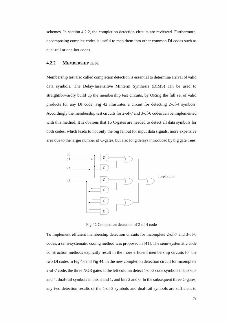
71
schemes. In section 4.2.2, the completion detection circuits are reviewed. Furthermore,
decomposing complex codes is useful to map them into other common DI codes such as
dual-rail or one-hot codes.
4.2.2 MEMBERSHIP TEST
Membership test also called completion detection is essential to determine arrival of valid
data symbols. The Delay-Insensitive Minterm Synthesis (DIMS) can be used to
straightforwardly build up the membership test circuits, by ORing the full set of valid
products for any DI code. Fig 42 illustrates a circuit for detecting 2-of-4 symbols.
Accordingly the membership test circuits for 2-of-7 and 3-of-6 codes can be implemented
with this method. It is obvious that 16 C-gates are needed to detect all data symbols for
both codes, which leads to not only the big fanout for input data signals, more expensive
area due to the larger number of C-gates, but also long delays introduced by big gate trees.
C
C
C
C
C
C
b0
b1
b2
b3completion
Fig 42 Completion detection of 2-of-4 code
To implement efficient membership detection circuits for incomplete 2-of-7 and 3-of-6
codes, a semi-systematic coding method was proposed in [41]. The semi-systematic code
construction methods explicitly result in the more efficient membership circuits for the
two DI codes in Fig 43 and Fig 44. In the new completion detection circuit for incomplete
2-of-7 code, the three NOR gates at the left column detect 1-of-3 code symbols in bits 6, 5
and 4, dual-rail symbols in bits 3 and 1, and bits 2 and 0. In the subsequent three C-gates,
any two detection results of the 1-of-3 symbols and dual-rail symbols are sufficient to
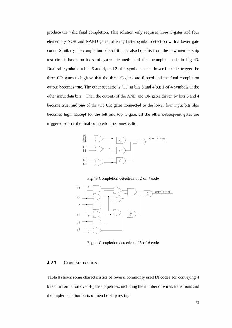
72
produce the valid final completion. This solution only requires three C-gates and four
elementary NOR and NAND gates, offering faster symbol detection with a lower gate
count. Similarly the completion of 3-of-6 code also benefits from the new membership
test circuit based on its semi-systematic method of the incomplete code in Fig 43.
Dual-rail symbols in bits 5 and 4, and 2-of-4 symbols at the lower four bits trigger the
three OR gates to high so that the three C-gates are flipped and the final completion
output becomes true. The other scenario is „11‟ at bits 5 and 4 but 1-of-4 symbols at the
other input data bits. Then the outputs of the AND and OR gates driven by bits 5 and 4
become true, and one of the two OR gates connected to the lower four input bits also
becomes high. Except for the left and top C-gate, all the other subsequent gates are
triggered so that the final completion becomes valid.
C
C
Cb0
b2
b1b3
b4b5b6
completion
Fig 43 Completion detection of 2-of-7 code
b0
b2
b1
b3
b4
b5
C
C
C
completion
Fig 44 Completion detection of 3-of-6 code
4.2.3 CODE SELECTION
Table 8 shows some characteristics of several commonly used DI codes for conveying 4
bits of information over 4-phase pipelines, including the number of wires, transitions and
the implementation costs of membership testing.
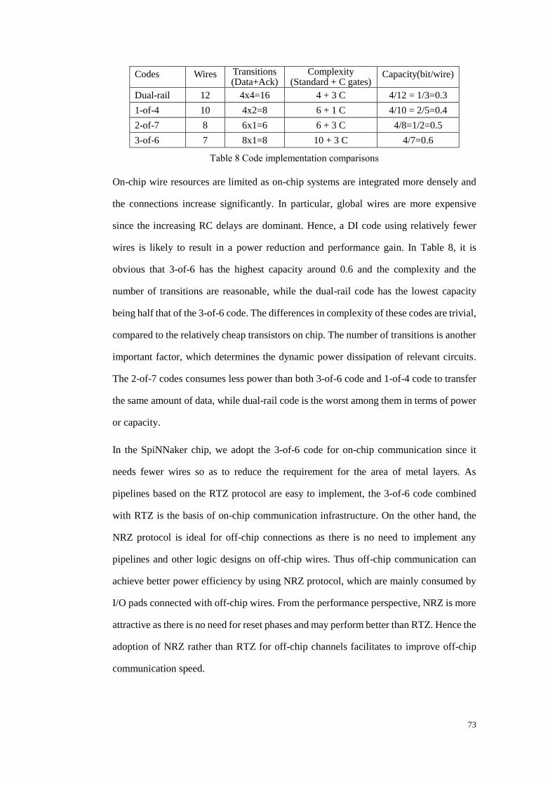
73
Codes Wires Transitions (Data+Ack)
Complexity (Standard + C gates)
Capacity(bit/wire)
Dual-rail 12 4x4=16 4 + 3 C 4/12 = 1/3=0.3
1-of-4 10 4x2=8 6 + 1 C 4/10 = 2/5=0.4
2-of-7 8 6x1=6 6 + 3 C 4/8=1/2=0.5
3-of-6 7 8x1=8 10 + 3 C 4/7=0.6
Table 8 Code implementation comparisons
On-chip wire resources are limited as on-chip systems are integrated more densely and
the connections increase significantly. In particular, global wires are more expensive
since the increasing RC delays are dominant. Hence, a DI code using relatively fewer
wires is likely to result in a power reduction and performance gain. In Table 8, it is
obvious that 3-of-6 has the highest capacity around 0.6 and the complexity and the
number of transitions are reasonable, while the dual-rail code has the lowest capacity
being half that of the 3-of-6 code. The differences in complexity of these codes are trivial,
compared to the relatively cheap transistors on chip. The number of transitions is another
important factor, which determines the dynamic power dissipation of relevant circuits.
The 2-of-7 codes consumes less power than both 3-of-6 code and 1-of-4 code to transfer
the same amount of data, while dual-rail code is the worst among them in terms of power
or capacity.
In the SpiNNaker chip, we adopt the 3-of-6 code for on-chip communication since it
needs fewer wires so as to reduce the requirement for the area of metal layers. As
pipelines based on the RTZ protocol are easy to implement, the 3-of-6 code combined
with RTZ is the basis of on-chip communication infrastructure. On the other hand, the
NRZ protocol is ideal for off-chip connections as there is no need to implement any
pipelines and other logic designs on off-chip wires. Thus off-chip communication can
achieve better power efficiency by using NRZ protocol, which are mainly consumed by
I/O pads connected with off-chip wires. From the performance perspective, NRZ is more
attractive as there is no need for reset phases and may perform better than RTZ. Hence the
adoption of NRZ rather than RTZ for off-chip channels facilitates to improve off-chip
communication speed.
74
4.2.4 CODE CONVERSION
Considering their simplicity, dual-rail or 1-of-4 codes are usually adopted to implement
logic circuits, while more complex n-of-m codes are usually used to increase
communication efficiency. Due to the use of different codes, conversion circuits are a
common concern. A semi-systematic method has been proposed to map DI symbols to
binary values [41]. Different mappings give different ordering to the DI codes, which
may affect the encoding and decoding complexity. By using the semi-systematic method
to determine the ordering, the complexity of the encoding and decoding circuits can be
significantly reduced. Encoding and decoding of various m-of-n codes from/to dual-rail
or 1-of-4 code can be implemented much more efficiently [41].
In the SpiNNaker chips, two different types of DI code are used for on-chip and off-chip
communication and conversion between the two codes is essential in the interface circuits.
In the transmitter, input data have to be converted from 3-of-6 into 2-of-7 symbols; in the
receiver, 2-of-7 symbols need be converted into 3-of-6 symbols before forwarding onto
the on-chip Communications NoC.
The code conversion between on-chip 3-of-6 and off-chip 2-of-7 codes is unique to
SpiNNaker. There is no need to use dual-rail code as the intermediate code in the
conversion as no dual-rail logic is required between pipeline registers in the off-chip
interfaces. The two codes can be translated directly in some way. All input 2-of-7 or
3-of-6 symbols need to be detected individually, as part of the completion detection
mechanism, and then mapped to the corresponding symbols of output code scheme.
These completion detection signals can be viewed as a 1-of-16 code in the transmitter and
a 1-of-17 code in the receiver, which involves additionally the detection of EoP. The
circuit implementation is detailed in the rest of this chapter.
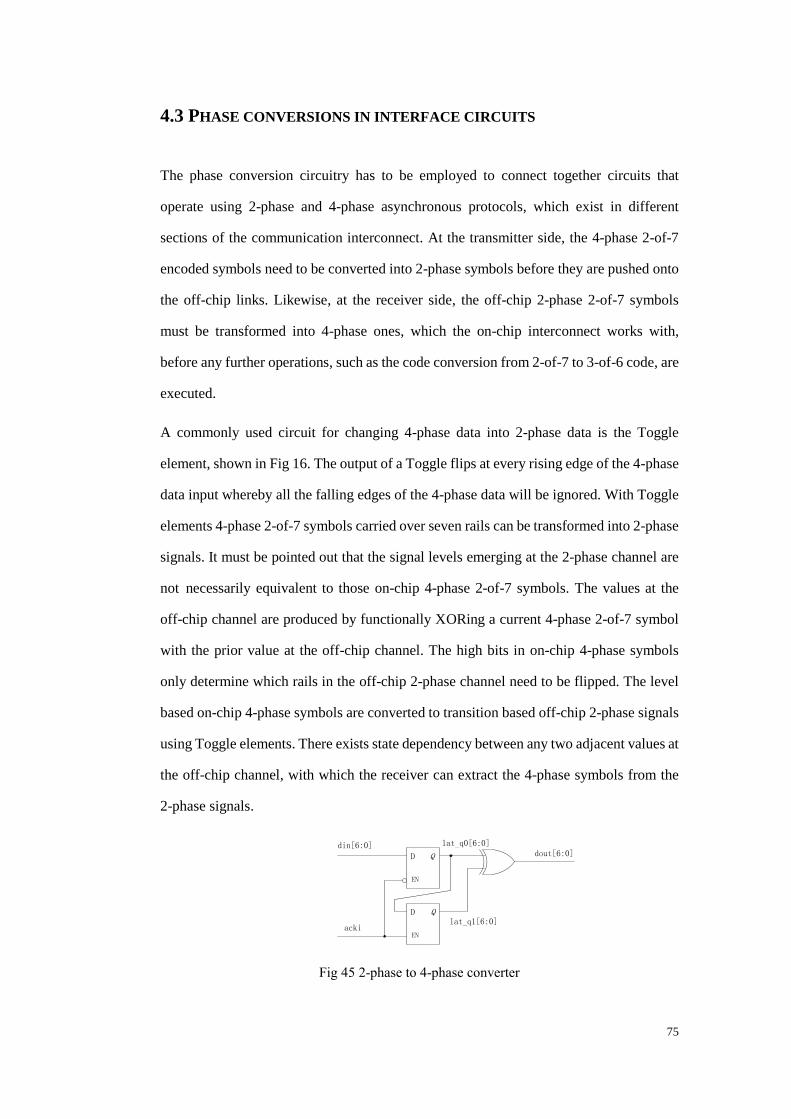
75
4.3 PHASE CONVERSIONS IN INTERFACE CIRCUITS
The phase conversion circuitry has to be employed to connect together circuits that
operate using 2-phase and 4-phase asynchronous protocols, which exist in different
sections of the communication interconnect. At the transmitter side, the 4-phase 2-of-7
encoded symbols need to be converted into 2-phase symbols before they are pushed onto
the off-chip links. Likewise, at the receiver side, the off-chip 2-phase 2-of-7 symbols
must be transformed into 4-phase ones, which the on-chip interconnect works with,
before any further operations, such as the code conversion from 2-of-7 to 3-of-6 code, are
executed.
A commonly used circuit for changing 4-phase data into 2-phase data is the Toggle
element, shown in Fig 16. The output of a Toggle flips at every rising edge of the 4-phase
data input whereby all the falling edges of the 4-phase data will be ignored. With Toggle
elements 4-phase 2-of-7 symbols carried over seven rails can be transformed into 2-phase
signals. It must be pointed out that the signal levels emerging at the 2-phase channel are
not necessarily equivalent to those on-chip 4-phase 2-of-7 symbols. The values at the
off-chip channel are produced by functionally XORing a current 4-phase 2-of-7 symbol
with the prior value at the off-chip channel. The high bits in on-chip 4-phase symbols
only determine which rails in the off-chip 2-phase channel need to be flipped. The level
based on-chip 4-phase symbols are converted to transition based off-chip 2-phase signals
using Toggle elements. There exists state dependency between any two adjacent values at
the off-chip channel, with which the receiver can extract the 4-phase symbols from the
2-phase signals.
D
EN
Q
D
EN
Q
acki
din[6:0]dout[6:0]
lat_q0[6:0]
lat_q1[6:0]
Fig 45 2-phase to 4-phase converter
76
In principle, transitions can be detected by comparing the levels before and after the
transitions occur. Two latches and one XOR gate for 1 bit of data are needed to perform
transition detection in Fig 45, where the output is a level signal. The data input din[6:0] is
2-phase, the data output dout[6:0] is 4phase, and acki is the acknowledge input from the
subsequent circuit. The circuit operates as follows: firstly the valid input data passes into
the upper latch and then the XOR gate to assert the output dout[6:0] since acki is initially
low. The top latch is then turned off and the bottom latch is turned on after dout[6:0] is
acknowledged by the subsequent circuit driving acki high, which means that the previous
data on the off-chip wires are stored in the both latches. The equivalent values of the two
latches drive the XOR gate to return to zero. After the zero values on dout[6:0] are
acknowledged by a low acki, the top latch is switched back on but the bottom one is
turned off. Hence the top latch is able to fetch new data while the previous data carried on
off-chip wires are still kept in the bottom latch. Once new data arrive, the XOR gate
compares the output from the latches which represent the current 2-of-7 and the prior
2-of-7 symbols and outputs a 2-of-7 symbol derived from the value on the off-chip wires.
The circuit comprising two latches and a XOR gate in Fig 45 can recognize whether a
transition occurs at the input wire. An off-chip channel in SpiNNaker requires 7 copies of
this circuit to detect all the 7 input data wires in the receiver; while another circuit is
needed at the transmitter side.
4.4 TRANSMITTER IMPLEMENTATION
The transmitter, shown in Fig 46 receiving data and control information, including EoPs,
from the neighbouring units of the on-chip Communications NoC, processes them
through separate data and control paths. The main functions of the transmitter are to
convert the data from 4-phase to 2-phase, to transform the data from 3-of-6 code into
2-of-7 code and to merge the two parallel data and control channels into one data channel
encoded with 2-of-7 code.
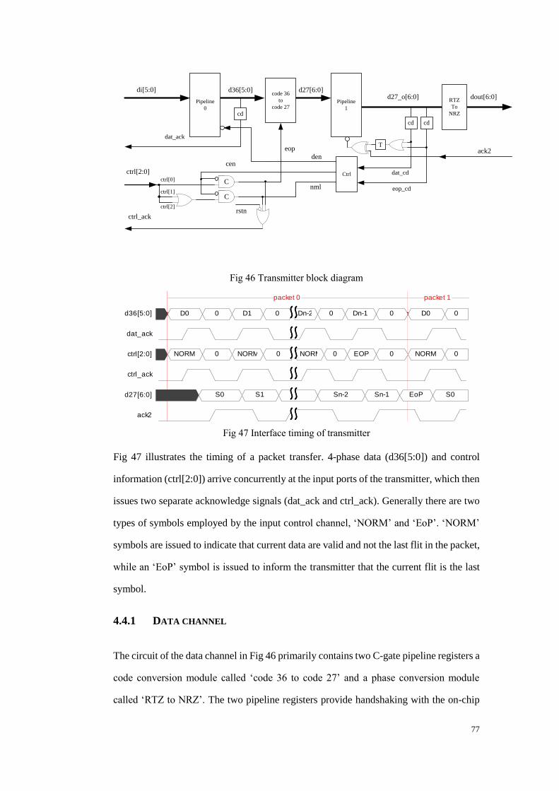
77
cd
Ctrl
di[5:0]
ctrl[0]
dat_ack
ctrl_ack
eop_cd
dat_cd
cenden
dout[6:0]
eop
code 36
to
code 27Pipeline
1
Pipeline
0
ack2
cd cd
d36[5:0] d27[6:0]
RTZ
To
NRZ
T
d27_o[6:0]
nmlctrl[1]
ctrl[2]
C
C
ctrl[2:0]
rstn
Fig 46 Transmitter block diagram
packet 0 packet 1
D0 0 D1 0 Dn-2 0 Dn-1 0 D0 0
NORM 0 NORM 0 NORM 0 EOP 0 NORM 0
S0 S1 Sn-2 Sn-1 EoP S0
d36[5:0]
dat_ack
ctrl[2:0]
ctrl_ack
d27[6:0]
ack2
Fig 47 Interface timing of transmitter
Fig 47 illustrates the timing of a packet transfer. 4-phase data (d36[5:0]) and control
information (ctrl[2:0]) arrive concurrently at the input ports of the transmitter, which then
issues two separate acknowledge signals (dat_ack and ctrl_ack). Generally there are two
types of symbols employed by the input control channel, „NORM‟ and „EoP‟. „NORM‟
symbols are issued to indicate that current data are valid and not the last flit in the packet,
while an „EoP‟ symbol is issued to inform the transmitter that the current flit is the last
symbol.
4.4.1 DATA CHANNEL
The circuit of the data channel in Fig 46 primarily contains two C-gate pipeline registers a
code conversion module called „code 36 to code 27‟ and a phase conversion module
called „RTZ to NRZ‟. The two pipeline registers provide handshaking with the on-chip
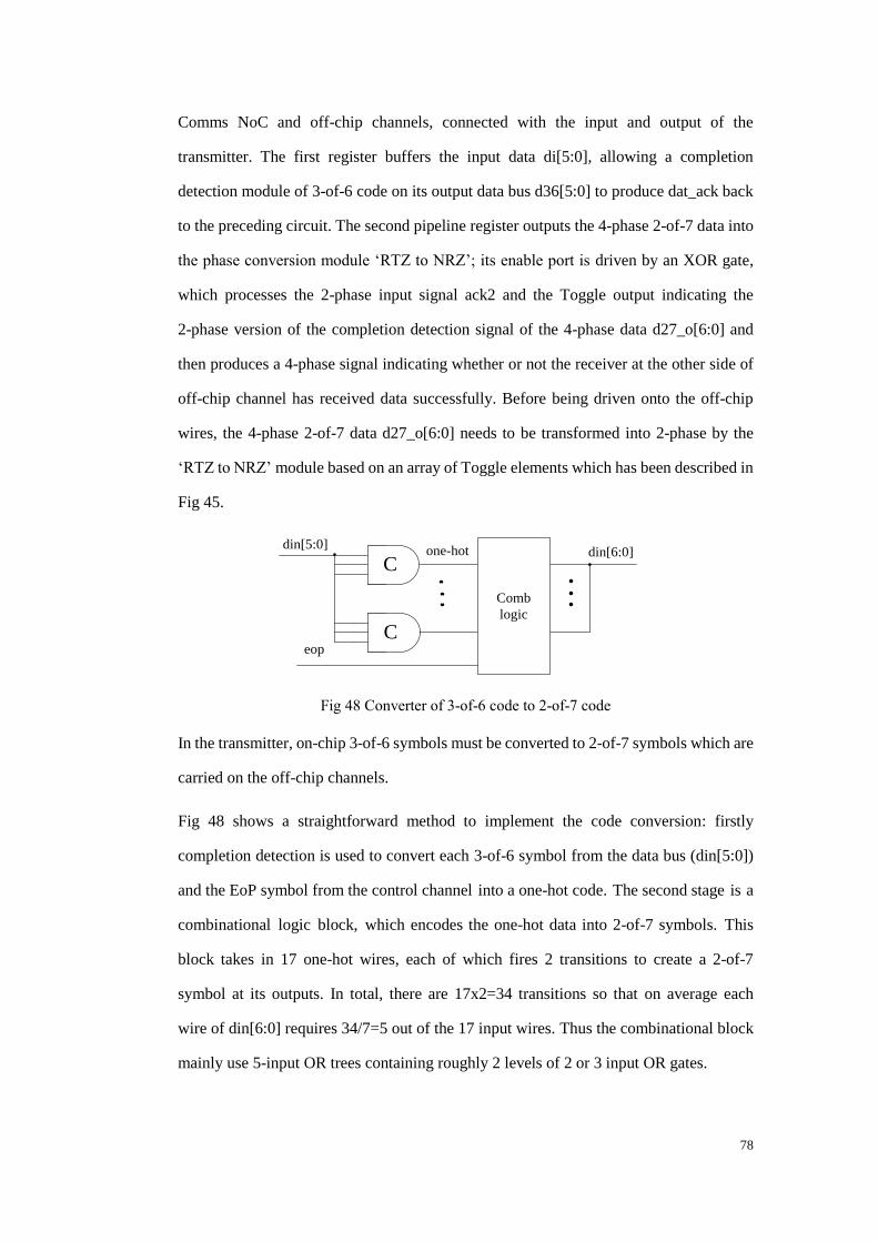
78
Comms NoC and off-chip channels, connected with the input and output of the
transmitter. The first register buffers the input data di[5:0], allowing a completion
detection module of 3-of-6 code on its output data bus d36[5:0] to produce dat_ack back
to the preceding circuit. The second pipeline register outputs the 4-phase 2-of-7 data into
the phase conversion module „RTZ to NRZ‟; its enable port is driven by an XOR gate,
which processes the 2-phase input signal ack2 and the Toggle output indicating the
2-phase version of the completion detection signal of the 4-phase data d27_o[6:0] and
then produces a 4-phase signal indicating whether or not the receiver at the other side of
off-chip channel has received data successfully. Before being driven onto the off-chip
wires, the 4-phase 2-of-7 data d27_o[6:0] needs to be transformed into 2-phase by the
„RTZ to NRZ‟ module based on an array of Toggle elements which has been described in
Fig 45.
C
C
Comb
logic
one-hotdin[5:0]
din[6:0]
eop
Fig 48 Converter of 3-of-6 code to 2-of-7 code
In the transmitter, on-chip 3-of-6 symbols must be converted to 2-of-7 symbols which are
carried on the off-chip channels.
Fig 48 shows a straightforward method to implement the code conversion: firstly
completion detection is used to convert each 3-of-6 symbol from the data bus (din[5:0])
and the EoP symbol from the control channel into a one-hot code. The second stage is a
combinational logic block, which encodes the one-hot data into 2-of-7 symbols. This
block takes in 17 one-hot wires, each of which fires 2 transitions to create a 2-of-7
symbol at its outputs. In total, there are 17x2=34 transitions so that on average each
wire of din[6:0] requires 34/7=5 out of the 17 input wires. Thus the combinational block
mainly use 5-input OR trees containing roughly 2 levels of 2 or 3 input OR gates.
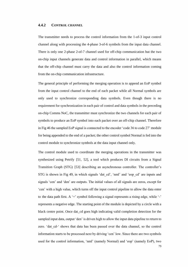
79
4.4.2 CONTROL CHANNEL
The transmitter needs to process the control information from the 1-of-3 input control
channel along with processing the 4-phase 3-of-6 symbols from the input data channel.
There is only one 2-phase 2-of-7 channel used for off-chip communication but the two
on-chip input channels generate data and control information in parallel, which means
that the off-chip channel must carry the data and also the control information coming
from the on-chip communication infrastructure.
The general principle of performing the merging operation is to append an EoP symbol
from the input control channel to the end of each packet while all Normal symbols are
only used to synchronize corresponding data symbols. Even though there is no
requirement for synchronization in each pair of control and data symbols in the preceding
on-chip Comms NoC, the transmitter must synchronize the two channels for each pair of
symbols to produce an EoP symbol into each packet over an off-chip channel. Therefore
in Fig 46 the sampled EoP signal is connected to the encoder „code 36 to code 27‟ module
for being appended to the end of a packet; the other control symbol Normal is fed into the
control module to synchronize symbols at the data input channel only.
The control module used to coordinate the merging operations in the transmitter was
synthesized using Petrify [51, 52], a tool which produces DI circuits from a Signal
Transition Graph (STG) [53] describing an asynchronous controller. The controller‟s
STG is shown in Fig 49, in which signals „dat_cd‟, „nml‟ and „eop_cd‟ are inputs and
signals „cen‟ and „den‟ are outputs. The initial values of all signals are zeros, except for
„cen‟ with a high value, which turns off the input control pipeline to allow the data enter
to the data path first. A „+‟ symbol following a signal represents a rising edge, while „-‟
represents a negative edge. The starting point of the module is depicted by a circle with a
black centre point. Once dat_cd goes high indicating valid completion detection for the
sampled input data, output „den‟ is driven high to allow the input data pipeline to return to
zero. „dat_cd-„ shows that data has been passed over the data channel, so the control
information starts to be processed next by driving „cen‟ low. Since there are two symbols
used for the control information, „nml‟ (namely Normal) and „eop‟ (namely EoP), two
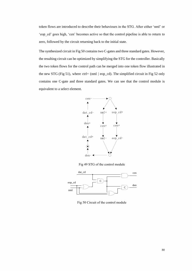
80
token flows are introduced to describe their behaviours in the STG. After either „nml‟ or
„eop_cd‟ goes high, „cen‟ becomes active so that the control pipeline is able to return to
zero, followed by the circuit returning back to the initial state.
The synthesized circuit in Fig 50 contains two C-gates and three standard gates. However,
the resulting circuit can be optimized by simplifying the STG for the controller. Basically
the two token flows for the control path can be merged into one token flow illustrated in
the new STG (Fig 51), where ctrl= (nml | eop_cd). The simplified circuit in Fig 52 only
contains one C-gate and three standard gates. We can see that the control module is
equivalent to a select element.
cen-
dat_cd-
den+
dat_cd+
den-
nml-
cen+
nml+ eop_cd+
cen+
eop_cd-
Fig 49 STG of the control module
C
C
cen
den
dat_cd
nml
eop_cd
Fig 50 Circuit of the control module
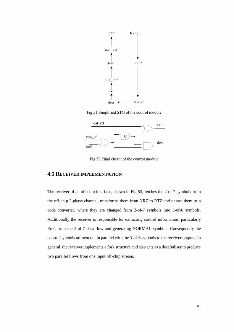
81
cen-
dat_cd-
den+
dat_cd+
den- ctrl-
cen+
ctrl+
Fig 51 Simplified STG of the control module
C
cen
den
dat_cd
nml
eop_cd
Fig 52 Final circuit of the control module
4.5 RECEIVER IMPLEMENTATION
The receiver of an off-chip interface, shown in Fig 53, fetches the 2-of-7 symbols from
the off-chip 2-phase channel, transforms them from NRZ to RTZ and passes them to a
code converter, where they are changed from 2-of-7 symbols into 3-of-6 symbols.
Additionally the receiver is responsible for extracting control information, particularly
EoP, from the 2-of-7 data flow and generating NORMAL symbols. Consequently the
control symbols are sent out in parallel with the 3-of-6 symbols to the receiver outputs. In
general, the receiver implements a fork structure and also acts as a deserialiser to produce
two parallel flows from one input off-chip stream.
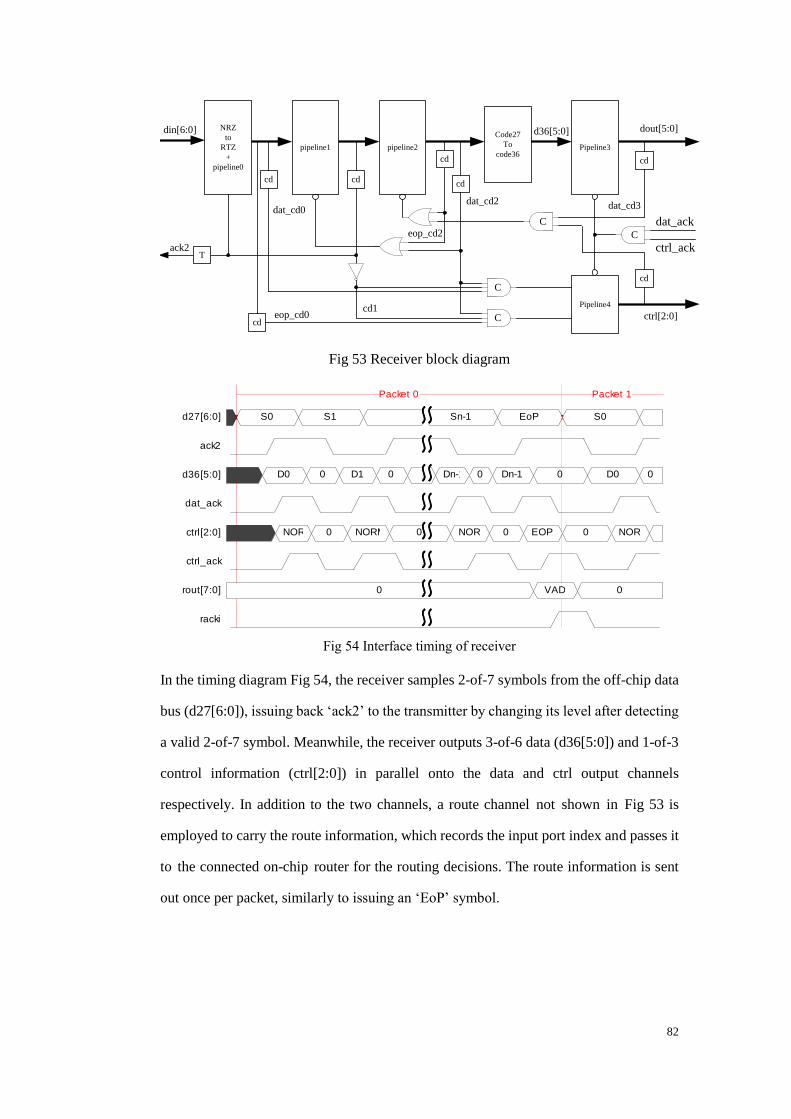
82
Pipeline3
dat_ack
ctrl_ack
dout[5:0]
ctrl[2:0]
d36[5:0]
cd
C
cd
C
cd C
Pipeline4
C
din[6:0]
ack2T
cd
cd
pipeline1 pipeline2
Code27
To
code36
NRZ
to
RTZ
+
pipeline0
cd
cd
eop_cd2
dat_cd2 dat_cd3dat_cd0
eop_cd0cd1
Fig 53 Receiver block diagram
Packet 0 Packet 1
S0 S1 Sn-1 EoP S0
D0 0 D1 0 Dn-1 0 Dn-1 0 D0 0
NORM 0 NORM 0 NORM 0 EOP 0 NORM
0 VAD 0
d27[6:0]
ack2
d36[5:0]
dat_ack
ctrl[2:0]
ctrl_ack
rout[7:0]
racki
Fig 54 Interface timing of receiver
In the timing diagram Fig 54, the receiver samples 2-of-7 symbols from the off-chip data
bus (d27[6:0]), issuing back „ack2‟ to the transmitter by changing its level after detecting
a valid 2-of-7 symbol. Meanwhile, the receiver outputs 3-of-6 data (d36[5:0]) and 1-of-3
control information (ctrl[2:0]) in parallel onto the data and ctrl output channels
respectively. In addition to the two channels, a route channel not shown in Fig 53 is
employed to carry the route information, which records the input port index and passes it
to the connected on-chip router for the routing decisions. The route information is sent
out once per packet, similarly to issuing an „EoP‟ symbol.

83
4.5.1 DATA CHANNEL
The 2-of-7 data have to travel through four pipeline registers over the data channel in the
receiver in Fig 53. The first register pipeline0 holds the output of phase converter which is
4-phase (RTZ) symbols of 2-of-7 code. The second register pipeline1 buffers the first
register output and sends back its completion detection signal as an acknowledgement to
the off-chip channel. The third register pipeline2 stores and forwards 2-of-7 symbols to
the code conversion module. The receiver treats data symbols and an EoP symbol
differently: the register pipeline2 is enabled by a valid EoP for a reset phase while it
cannot be reset until data symbols are forwarded to the receiver‟s output channels. The
final register pipeline3 captures the output 3-of-6 symbols of the combinational block
„Code27 to code36‟ and forwards them onto the output data channel.
Note that there are two C-gates in the receiver to synchronize the data and control
channels. The first C-gate collects the acknowledge signals dat_ack and ctrl_ack from the
output data and control channels for correct operations performed at the register pipeline2;
the other synchronizes the output data and control channels. This enforced
synchronization on the output data and control channels helps to recover the control
symbols and greatly simplifies the receiver circuit implementation.
4.5.2 CONTROL CHANNEL
The information propagating over the output control channel is extracted from the 2-of-7
data flow on the off-chip channel. There are two symbols used in the control information,
Normal and EoP. The interface between the receiver and the on-chip communication
infrastructure requires that the control information corresponding to the last symbol
within a packet at the data channel must be an EoP, all other data symbols in a packet
must be Normal symbols.
To design a circuit meeting this requirement, two extra pipeline registers are needed after
the input register pipeline0 so as to buffer two 2-of-7 symbols. Thus these three pipeline
registers can store, at most, two data symbols or a data and an EoP symbols. A Normal
symbol is issued if the two stored 2-of-7 symbols are both data symbols; an EoP symbol is
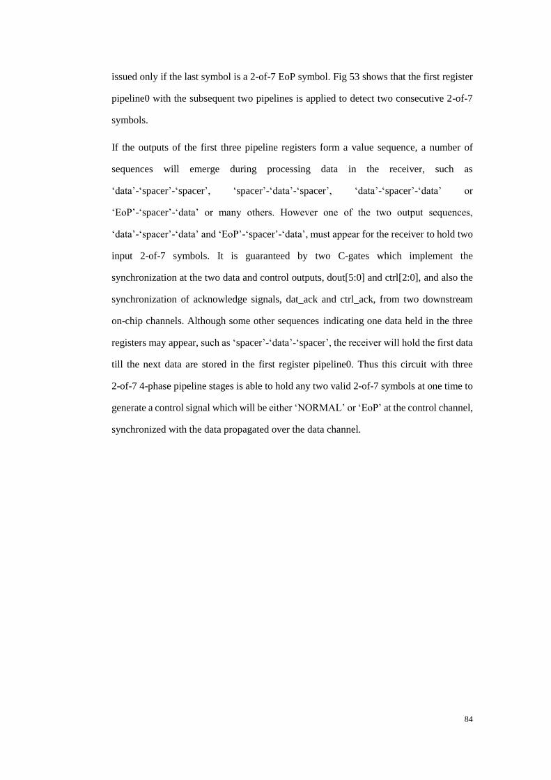
84
issued only if the last symbol is a 2-of-7 EoP symbol. Fig 53 shows that the first register
pipeline0 with the subsequent two pipelines is applied to detect two consecutive 2-of-7
symbols.
If the outputs of the first three pipeline registers form a value sequence, a number of
sequences will emerge during processing data in the receiver, such as
„data‟-„spacer‟-„spacer‟, „spacer‟-„data‟-„spacer‟, „data‟-„spacer‟-„data‟ or
„EoP‟-„spacer‟-„data‟ or many others. However one of the two output sequences,
„data‟-„spacer‟-„data‟ and „EoP‟-„spacer‟-„data‟, must appear for the receiver to hold two
input 2-of-7 symbols. It is guaranteed by two C-gates which implement the
synchronization at the two data and control outputs, dout[5:0] and ctrl[2:0], and also the
synchronization of acknowledge signals, dat_ack and ctrl_ack, from two downstream
on-chip channels. Although some other sequences indicating one data held in the three
registers may appear, such as „spacer‟-„data‟-„spacer‟, the receiver will hold the first data
till the next data are stored in the first register pipeline0. Thus this circuit with three
2-of-7 4-phase pipeline stages is able to hold any two valid 2-of-7 symbols at one time to
generate a control signal which will be either „NORMAL‟ or „EoP‟ at the control channel,
synchronized with the data propagated over the data channel.
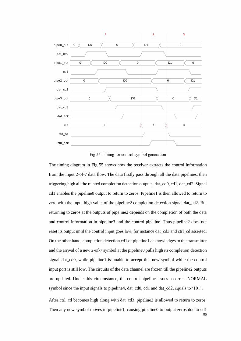
85
1 2 3
0 D0 0 D1 0
0 D0 0 D1 0
0 D0 0 D1
0 D0 0 D1
0 C0 0
pipe0_out
dat_cd0
pipe1_out
cd1
pipe2_out
dat_cd2
pipe3_out
dat_cd3
dat_ack
ctrl
ctrl_cd
ctrl_ack
Fig 55 Timing for control symbol generation
The timing diagram in Fig 55 shows how the receiver extracts the control information
from the input 2-of-7 data flow. The data firstly pass through all the data pipelines, then
triggering high all the related completion detection outputs, dat_cd0, cd1, dat_cd2. Signal
cd1 enables the pipeline0 output to return to zeros. Pipeline1 is then allowed to return to
zero with the input high value of the pipeline2 completion detection signal dat_cd2. But
returning to zeros at the outputs of pipeline2 depends on the completion of both the data
and control information in pipeline3 and the control pipeline. Thus pipeline2 does not
reset its output until the control input goes low, for instance dat_cd3 and ctrl_cd asserted.
On the other hand, completion detection cd1 of pipeline1 acknowledges to the transmitter
and the arrival of a new 2-of-7 symbol at the pipeline0 pulls high its completion detection
signal dat_cd0, while pipeline1 is unable to accept this new symbol while the control
input port is still low. The circuits of the data channel are frozen till the pipeline2 outputs
are updated. Under this circumstance, the control pipeline issues a correct NORMAL
symbol since the input signals to pipeline4, dat_cd0, cd1 and dat_cd2, equals to „101‟.
After ctrl_cd becomes high along with dat_cd3, pipeline2 is allowed to return to zeros.
Then any new symbol moves to pipeline1, causing pipeline0 to output zeros due to cd1
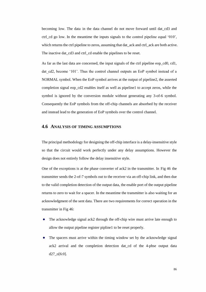
86
becoming low. The data in the data channel do not move forward until dat_cd3 and
ctrl_cd go low. In the meantime the inputs signals to the control pipeline equal „010‟,
which returns the ctrl pipeline to zeros, assuming that dat_ack and ctrl_ack are both active.
The inactive dat_cd3 and ctrl_cd enable the pipelines to be reset.
As far as the last data are concerned, the input signals of the ctrl pipeline eop_cd0, cd1,
dat_cd2, become „101‟. Thus the control channel outputs an EoP symbol instead of a
NORMAL symbol. When the EoP symbol arrives at the output of pipeline2, the asserted
completion signal eop_cd2 enables itself as well as pipeline1 to accept zeros, while the
symbol is ignored by the conversion module without generating any 3-of-6 symbol.
Consequently the EoP symbols from the off-chip channels are absorbed by the receiver
and instead lead to the generation of EoP symbols over the control channel.
4.6 ANALYSIS OF TIMING ASSUMPTIONS
The principal methodology for designing the off-chip interface is a delay-insensitive style
so that the circuit would work perfectly under any delay assumptions. However the
design does not entirely follow the delay insensitive style.
One of the exceptions is at the phase converter of ack2 in the transmitter. In Fig 46 the
transmitter sends the 2-of-7 symbols out to the receiver via an off-chip link, and then due
to the valid completion detection of the output data, the enable port of the output pipeline
returns to zero to wait for a spacer. In the meantime the transmitter is also waiting for an
acknowledgment of the sent data. There are two requirements for correct operation in the
transmitter in Fig 46:
The acknowledge signal ack2 through the off-chip wire must arrive late enough to
allow the output pipeline register pipline1 to be reset properly.
The spacers must arrive within the timing window set by the acknowledge signal
ack2 arrival and the completion detection dat_cd of the 4-phse output data
d27_o[6:0].
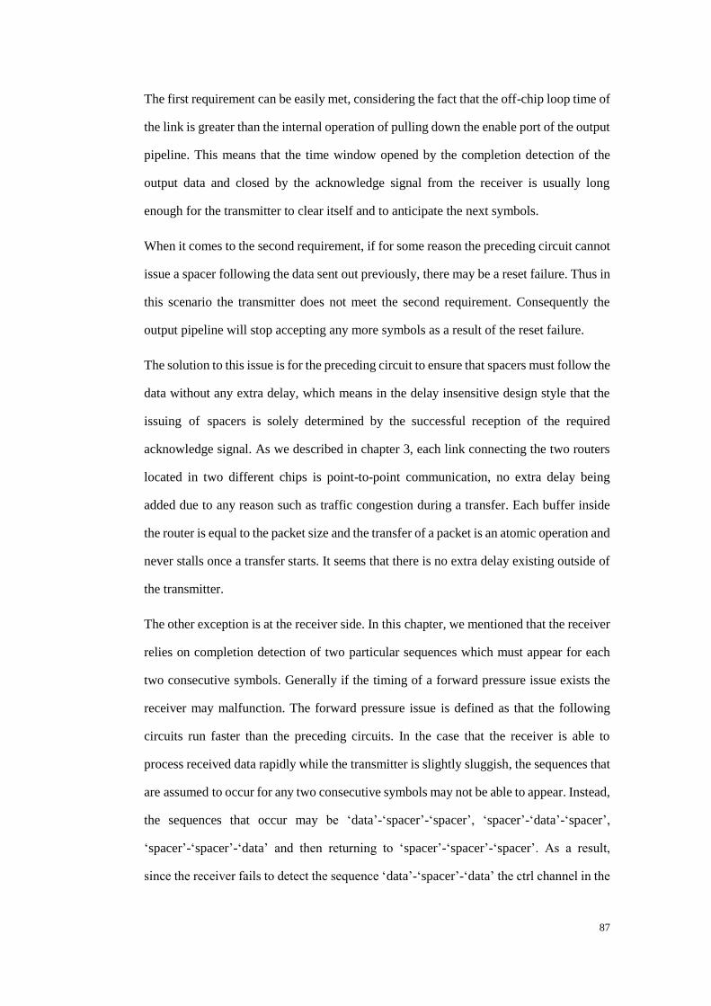
87
The first requirement can be easily met, considering the fact that the off-chip loop time of
the link is greater than the internal operation of pulling down the enable port of the output
pipeline. This means that the time window opened by the completion detection of the
output data and closed by the acknowledge signal from the receiver is usually long
enough for the transmitter to clear itself and to anticipate the next symbols.
When it comes to the second requirement, if for some reason the preceding circuit cannot
issue a spacer following the data sent out previously, there may be a reset failure. Thus in
this scenario the transmitter does not meet the second requirement. Consequently the
output pipeline will stop accepting any more symbols as a result of the reset failure.
The solution to this issue is for the preceding circuit to ensure that spacers must follow the
data without any extra delay, which means in the delay insensitive design style that the
issuing of spacers is solely determined by the successful reception of the required
acknowledge signal. As we described in chapter 3, each link connecting the two routers
located in two different chips is point-to-point communication, no extra delay being
added due to any reason such as traffic congestion during a transfer. Each buffer inside
the router is equal to the packet size and the transfer of a packet is an atomic operation and
never stalls once a transfer starts. It seems that there is no extra delay existing outside of
the transmitter.
The other exception is at the receiver side. In this chapter, we mentioned that the receiver
relies on completion detection of two particular sequences which must appear for each
two consecutive symbols. Generally if the timing of a forward pressure issue exists the
receiver may malfunction. The forward pressure issue is defined as that the following
circuits run faster than the preceding circuits. In the case that the receiver is able to
process received data rapidly while the transmitter is slightly sluggish, the sequences that
are assumed to occur for any two consecutive symbols may not be able to appear. Instead,
the sequences that occur may be „data‟-„spacer‟-„spacer‟, „spacer‟-„data‟-„spacer‟,
„spacer‟-„spacer‟-„data‟ and then returning to „spacer‟-„spacer‟-„spacer‟. As a result,
since the receiver fails to detect the sequence „data‟-„spacer‟-„data‟ the ctrl channel in the

88
receiver collapses and fails to recover control symbols. The receiver forces the two output
data and control channels to be synchronous and so to avoid sequence detection failures.
4.7 SUMMARY
This chapter described the original design of the off-chip interface without considering
tolerance to transient faults. The transmitter and receiver were designed mainly in a
delay-insensitive style, though timing assumptions are required in the phase converters.
This original design is functional with realistic timing assumptions as was confirmed by
circuit simulation with approximated circuit delays. In current design methodologies,
the tolerance of logic circuits to transient faults is not particularly considered.
The impact of transient faults on the SpiNNaker inter-chip communication links will be
investigated in the next chapter. The original design presented here as a baseline will be
revised to deliverimproved fault tolerance.
89
Chapter 5 FAULT TOLERANCE ANALYSIS OF GLOBAL DI
PIPELINES
This chapter first introduces the sensitivity of C-gates to transient faults, followed by
discussion on the sensitivity of 4-phase DI pipelines and two 2-phase pipelines
Micropipeline and Mousetrap. The behaviour of several key hardware modules in the
off-chip interface circuits is finally analysed in the presence of transient glitches.
5.1 FAULT SENSITIVITY OF C-GATES
As elementary components, C-gates are used widely in most kinds of DI pipelines; the
sensitivity to transient faults in the DI communication pipelines is analyzed.
C-gates sensitivity to faults was analyzed [54]. For a 2-input C-gate, there are four
possible states at its output due to any change at its inputs. In Fig 56, the first two states
will not be affected by any glitch at either of its inputs. In (c), the 2-input C-gate is
sensitive to a glitch occurring at the upper input, which may flip the output value from 0
to 1, though the lower input is immune to any glitch in this situation as the output is
already low. Similarly in Fig 56 (d), the C-gate is sensitive to a glitch at the lower input.
During the stable states, the probability of vulnerability to an input glitch is 1/2.
C0
00
C1
11
C0
10
C0
11
(a) (b) (c) (d)
Fig 56 2-input C-gate in different situations
For a multiple input C-gate (assuming 4 inputs), there are eight stable states. In Fig 57, in
the first six states (only two as examples shown here at (a) and (b)) a single glitch cannot
change the output, whereas only the last two states at (c) and (d) are vulnerable to a glitch
at a specific input. The vulnerability probability is only 1/4, half that of a 2-input C-gate.

90
Thus a 2-input C-gate is more vulnerable to a single transient fault than a multiple input
C-gate.
C0
10
1
0
C0
11
1
0
C1
10
1
0
C0
01
0
1
(a) (b) (c) (d)
Fig 57 M-input C-gate in different situations
C-gates and latches behave differently when subjected to transient faults, shown in Fig
58. C-gates as a state holding unit are able to propagate only one edge of a short glitch in
their sensitive state. The C-gate in Fig 58 (a) propagates a rising edge, while the C-gate in
Fig 58 (b) propagates a falling edge. By contrast, a transparent latch is able to pass both
two edges of a short glitch, shown in Fig 58 (c). However, this might not always be true.
At the two edges of a long glitch, for example, if the input changes at the enable port of a
latch or the lower port of a C-gate, the C-gate may be able to pass both two edges while
the latch may only allow one edge to propagate through.
C1
(a)
C0
(b)
latch
en
i o
1
(c)
Fig 58 Glitches at a C-gate and a latch
5.2 FAULT SENSITIVITY OF 4-PHASE DI PIPELINES
5.2.1 DUAL-RAIL PIPELINES BASED ON C-GATES
Based on the introduction to C-gate sensitivity, DI pipelines implemented with C-gates
are discussed in this section. The dual-rail pipeline carrying one bit is the simplest DI
data pipeline. There is only one C-gate used in every pipeline stage. As we introduced in
Fig 24, the second port of each C-gate acts as an enable port, inverting the acknowledge
signal back from the subsequent pipeline stage. The acknowledge signal is obtained by
ORing two outputs of each stage. The sensitivity of a dual-rail is the same as a C-gate we
discussed previously, with the probability of 1/2.
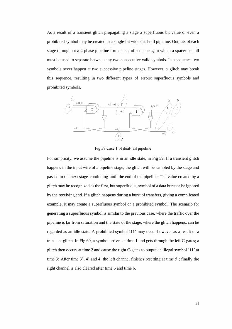
91
As a result of a transient glitch propagating a stage a superfluous bit value or even a
prohibited symbol may be created in a single-bit wide dual-rail pipeline. Outputs of each
stage throughout a 4-phase pipeline forms a set of sequences, in which a spacer or null
must be used to separate between any two consecutive valid symbols. In a sequence two
symbols never happen at two successive pipeline stages. However, a glitch may break
this sequence, resulting in two different types of errors: superfluous symbols and
prohibited symbols.
CC C
d0[1:0]
d2[1:0]d1[1:0]
ack1 ack2
ack3
00
01
0
14
1 23
0
0
6
0 1
5
Fig 59 Case 1 of dual-rail pipeline
For simplicity, we assume the pipeline is in an idle state, in Fig 59. If a transient glitch
happens in the input wire of a pipeline stage, the glitch will be sampled by the stage and
passed to the next stage continuing until the end of the pipeline. The value created by a
glitch may be recognized as the first, but superfluous, symbol of a data burst or be ignored
by the receiving end. If a glitch happens during a burst of transfers, giving a complicated
example, it may create a superfluous symbol or a prohibited symbol. The scenario for
generating a superfluous symbol is similar to the previous case, where the traffic over the
pipeline is far from saturation and the state of the stage, where the glitch happens, can be
regarded as an idle state. A prohibited symbol „11‟ may occur however as a result of a
transient glitch. In Fig 60, a symbol arrives at time 1 and gets through the left C-gates; a
glitch then occurs at time 2 and cause the right C-gates to output an illegal symbol „11‟ at
time 3; After time 3‟, 4‟ and 4, the left channel finishes resetting at time 5‟; finally the
right channel is also cleared after time 5 and time 6.
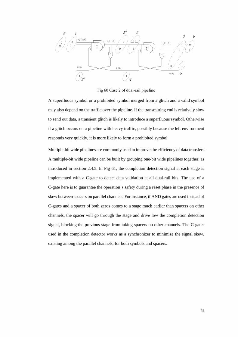
92
CC C
d0[1:0]
d2[1:0]d1[1:0]
ack1 ack2
ack3
10
11
1
1
0 1
0
0
1 23
5
4
6
00
4'
13'
0
5'
0
Fig 60 Case 2 of dual-rail pipeline
A superfluous symbol or a prohibited symbol merged from a glitch and a valid symbol
may also depend on the traffic over the pipeline. If the transmitting end is relatively slow
to send out data, a transient glitch is likely to introduce a superfluous symbol. Otherwise
if a glitch occurs on a pipeline with heavy traffic, possibly because the left environment
responds very quickly, it is more likely to form a prohibited symbol.
Multiple-bit wide pipelines are commonly used to improve the efficiency of data transfers.
A multiple-bit wide pipeline can be built by grouping one-bit wide pipelines together, as
introduced in section 2.4.5. In Fig 61, the completion detection signal at each stage is
implemented with a C-gate to detect data validation at all dual-rail bits. The use of a
C-gate here is to guarantee the operation‟s safety during a reset phase in the presence of
skew between spacers on parallel channels. For instance, if AND gates are used instead of
C-gates and a spacer of both zeros comes to a stage much earlier than spacers on other
channels, the spacer will go through the stage and drive low the completion detection
signal, blocking the previous stage from taking spacers on other channels. The C-gates
used in the completion detector works as a synchronizer to minimize the signal skew,
existing among the parallel channels, for both symbols and spacers.
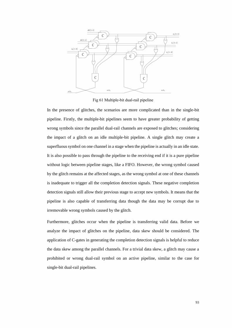
93
CC C
d0[1:0]
d2[1:0]
ack1ack2 ack3
CC C
d0[3:2]
d2[3:2]
CC C
C C
d0[5:4]
d2[5:4]
Fig 61 Multiple-bit dual-rail pipeline
In the presence of glitches, the scenarios are more complicated than in the single-bit
pipeline. Firstly, the multiple-bit pipelines seem to have greater probability of getting
wrong symbols since the parallel dual-rail channels are exposed to glitches; considering
the impact of a glitch on an idle multiple-bit pipeline. A single glitch may create a
superfluous symbol on one channel in a stage when the pipeline is actually in an idle state.
It is also possible to pass through the pipeline to the receiving end if it is a pure pipeline
without logic between pipeline stages, like a FIFO. However, the wrong symbol caused
by the glitch remains at the affected stages, as the wrong symbol at one of these channels
is inadequate to trigger all the completion detection signals. These negative completion
detection signals still allow their previous stage to accept new symbols. It means that the
pipeline is also capable of transferring data though the data may be corrupt due to
irremovable wrong symbols caused by the glitch.
Furthermore, glitches occur when the pipeline is transferring valid data. Before we
analyze the impact of glitches on the pipeline, data skew should be considered. The
application of C-gates in generating the completion detection signals is helpful to reduce
the data skew among the parallel channels. For a trivial data skew, a glitch may cause a
prohibited or wrong dual-rail symbol on an active pipeline, similar to the case for
single-bit dual-rail pipelines.
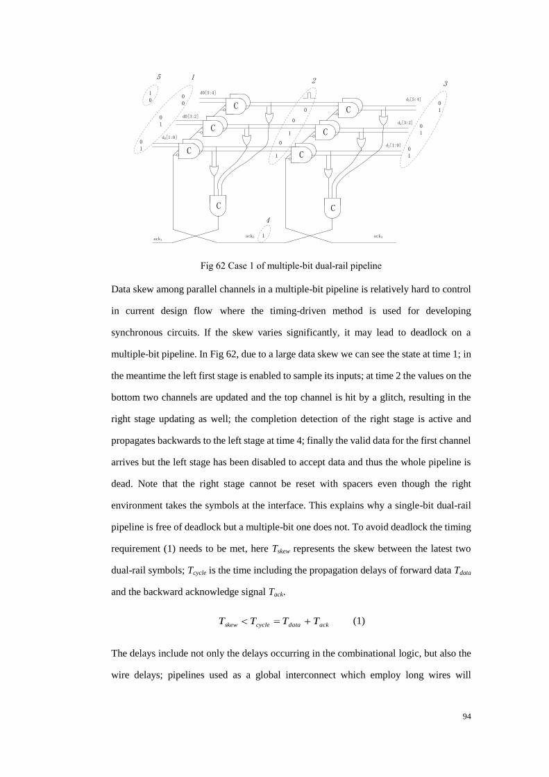
94
CC C
d0[1:0]
d2[1:0]
ack1ack2 ack3
CC C
d0[3:2]
d2[3:2]
CC C
C C
d0[5:4]
d2[5:4]
10
10
00
0
0
0
1
1
10
10
10
1 2 3
1
4
1
0
5
Fig 62 Case 1 of multiple-bit dual-rail pipeline
Data skew among parallel channels in a multiple-bit pipeline is relatively hard to control
in current design flow where the timing-driven method is used for developing
synchronous circuits. If the skew varies significantly, it may lead to deadlock on a
multiple-bit pipeline. In Fig 62, due to a large data skew we can see the state at time 1; in
the meantime the left first stage is enabled to sample its inputs; at time 2 the values on the
bottom two channels are updated and the top channel is hit by a glitch, resulting in the
right stage updating as well; the completion detection of the right stage is active and
propagates backwards to the left stage at time 4; finally the valid data for the first channel
arrives but the left stage has been disabled to accept data and thus the whole pipeline is
dead. Note that the right stage cannot be reset with spacers even though the right
environment takes the symbols at the interface. This explains why a single-bit dual-rail
pipeline is free of deadlock but a multiple-bit one does not. To avoid deadlock the timing
requirement (1) needs to be met, here Tskew represents the skew between the latest two
dual-rail symbols; Tcycle is the time including the propagation delays of forward data Tdata
and the backward acknowledge signal Tack.
ackdatacycleskew TTTT (1)
The delays include not only the delays occurring in the combinational logic, but also the
wire delays; pipelines used as a global interconnect which employ long wires will
95
introduce relatively significant wire delays in a complex SoC, raising an actual challenge
to meet the timing requirement.
We discuss the scenarios of pure single or multiple-bit pipelines. For a dual-rail pipeline
integrated with dual-rail combinational logic, glitches will lead to different impacts on the
circuits. As discussed in section 2.3.3, a dual-rail logic circuit implemented with DIMS or
an equivalent QDI technique waits for all dual-rail symbols arriving at its inputs and
therefore a superfluous symbol on one of the channels cannot propagate alone from the
next stage‟s inputs to the end of the pipeline. Therefore a wrong symbol is restricted
within one stage of the pipeline but it is still possible to corrupt the next valid data. In the
deadlock scenario on a multiple-bit pipeline, the delay of the combinational logic
increases Tcycle and thus enhances the resistance to deadlock.
5.2.2 1-OF-4 PIPELINES
A single-bit pipeline using 1-of-4 code can be viewed as the extension of a single-bit
dual-rail pipeline. In Fig 63 one stage comprises four C-gates; the completion detection
unit is simply a 4 input OR gate. The fault effects are also similar to the single-bit
dual-rail pipeline; it does not stall but introduces wrong or prohibited symbols in the
presence of transient glitches.
A multiple-bit 1-of-4 pipeline is built in a similar way as a multiple-bit dual-rail pipeline
in Fig 64. The example in the figure integrates twelve wires of three single 1-of-4
channels to carry 6 bit data. We can have 1-of-4 pipelines with a data width of 8 bits or 16
bits by grouping more channels together. In response to glitches, a multiple-bit 1-of-4
pipeline suffers from similar fault effects, introducing wrong or prohibited symbols. The
most significant impact among them is deadlock which eventually stalls the pipelines.
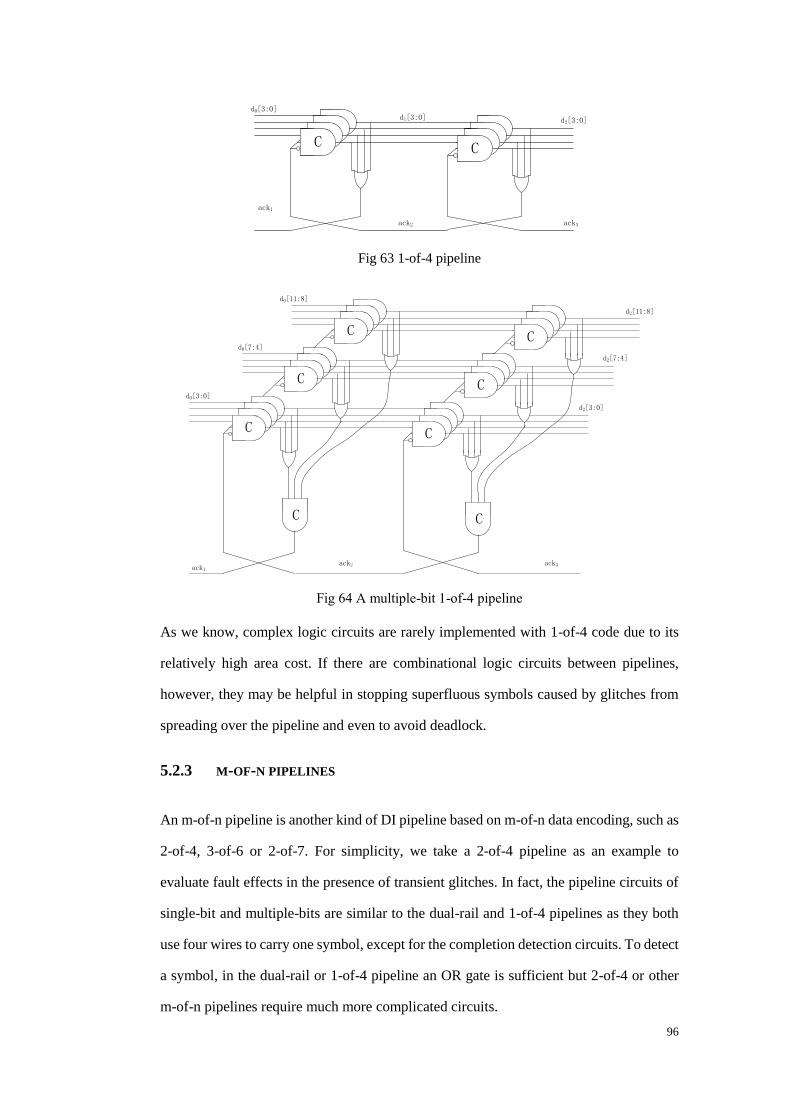
96
CCCC C
d0[3:0]
d2[3:0]d1[3:0]
ack1
ack2 ack3
Fig 63 1-of-4 pipeline
CCCC C
d0[3:0]
d2[3:0]
ack1ack2 ack3
CCCC C
d0[7:4]
d2[7:4]
CCCC C
C C
d0[11:8]
d2[11:8]
Fig 64 A multiple-bit 1-of-4 pipeline
As we know, complex logic circuits are rarely implemented with 1-of-4 code due to its
relatively high area cost. If there are combinational logic circuits between pipelines,
however, they may be helpful in stopping superfluous symbols caused by glitches from
spreading over the pipeline and even to avoid deadlock.
5.2.3 M-OF-N PIPELINES
An m-of-n pipeline is another kind of DI pipeline based on m-of-n data encoding, such as
2-of-4, 3-of-6 or 2-of-7. For simplicity, we take a 2-of-4 pipeline as an example to
evaluate fault effects in the presence of transient glitches. In fact, the pipeline circuits of
single-bit and multiple-bits are similar to the dual-rail and 1-of-4 pipelines as they both
use four wires to carry one symbol, except for the completion detection circuits. To detect
a symbol, in the dual-rail or 1-of-4 pipeline an OR gate is sufficient but 2-of-4 or other
m-of-n pipelines require much more complicated circuits.
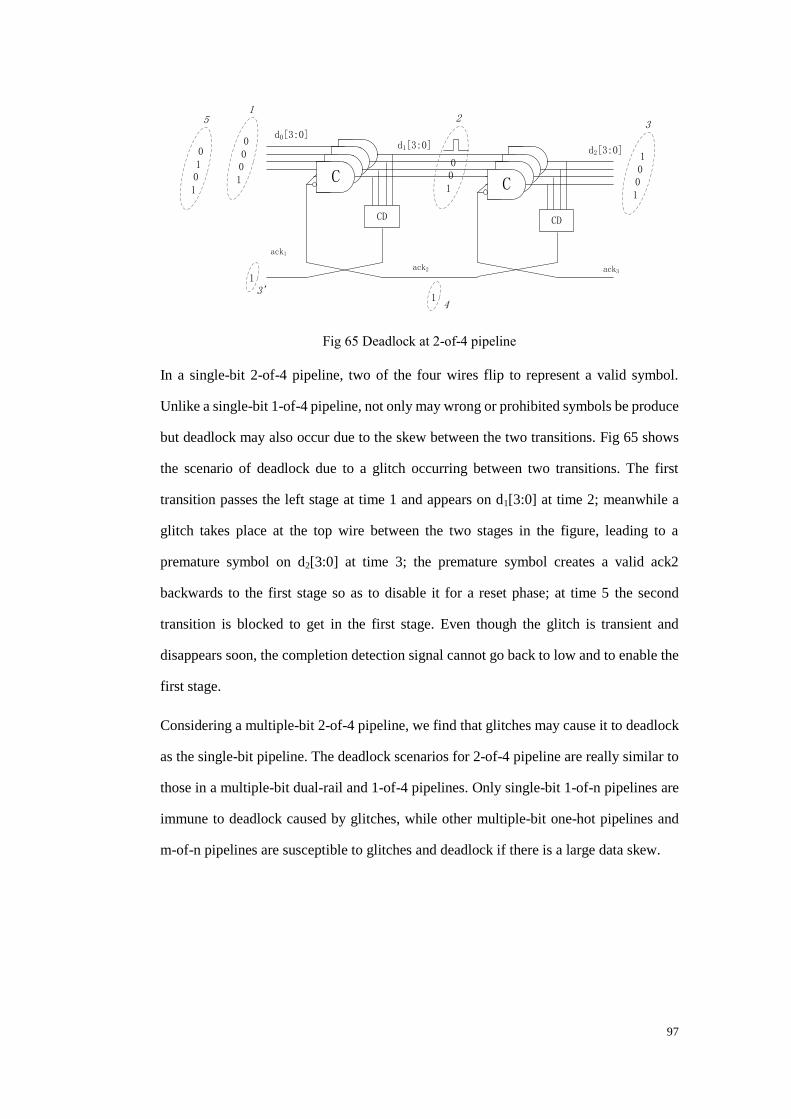
97
CCCC C
d0[3:0]
d2[3:0]d1[3:0]
ack1
ack2 ack3
CD CD
00
1
10 0
2
10
01
3
10
10
5
10
14
3'1
Fig 65 Deadlock at 2-of-4 pipeline
In a single-bit 2-of-4 pipeline, two of the four wires flip to represent a valid symbol.
Unlike a single-bit 1-of-4 pipeline, not only may wrong or prohibited symbols be produce
but deadlock may also occur due to the skew between the two transitions. Fig 65 shows
the scenario of deadlock due to a glitch occurring between two transitions. The first
transition passes the left stage at time 1 and appears on d1[3:0] at time 2; meanwhile a
glitch takes place at the top wire between the two stages in the figure, leading to a
premature symbol on d2[3:0] at time 3; the premature symbol creates a valid ack2
backwards to the first stage so as to disable it for a reset phase; at time 5 the second
transition is blocked to get in the first stage. Even though the glitch is transient and
disappears soon, the completion detection signal cannot go back to low and to enable the
first stage.
Considering a multiple-bit 2-of-4 pipeline, we find that glitches may cause it to deadlock
as the single-bit pipeline. The deadlock scenarios for 2-of-4 pipeline are really similar to
those in a multiple-bit dual-rail and 1-of-4 pipelines. Only single-bit 1-of-n pipelines are
immune to deadlock caused by glitches, while other multiple-bit one-hot pipelines and
m-of-n pipelines are susceptible to glitches and deadlock if there is a large data skew.
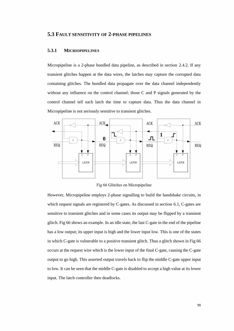
98
5.3 FAULT SENSITIVITY OF 2-PHASE PIPELINES
5.3.1 MICRIOPIPELINES
Micropipeline is a 2-phase bundled data pipeline, as described in section 2.4.2. If any
transient glitches happen at the data wires, the latches may capture the corrupted data
containing glitches. The bundled data propagate over the data channel independently
without any influence on the control channel; those C and P signals generated by the
control channel tell each latch the time to capture data. Thus the data channel in
Micropipeline is not seriously sensitive to transient glitches.
Fig 66 Glitches on Micropipeline
However, Micropipeline employs 2-phase signalling to build the handshake circuits, in
which request signals are registered by C-gates. As discussed in section 6.1, C-gates are
sensitive to transient glitches and in some cases its output may be flipped by a transient
glitch. Fig 66 shows an example. In an idle state, the last C-gate in the end of the pipeline
has a low output; its upper input is high and the lower input low. This is one of the states
in which C-gate is vulnerable to a positive transient glitch. Thus a glitch shown in Fig 66
occurs at the request wire which is the lower input of the final C-gate, causing the C-gate
output to go high. This asserted output travels back to flip the middle C-gate upper input
to low. It can be seen that the middle C-gate is disabled to accept a high value at its lower
input. The latch controller then deadlocks.
CC
ACK ACK
REQ REQ
ACK
REQ
LATCH LATCH
C P C P
C
LATCH
C P
ACK
REQ
1 0
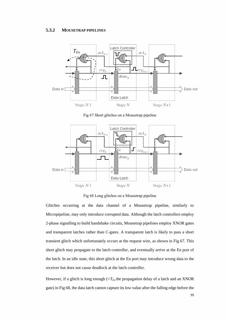
99
5.3.2 MOUSETRAP PIPELINES
Fig 67 Short glitches on a Mousetrap pipeline
Fig 68 Long glitches on a Mousetrap pipeline
Glitches occurring at the data channel of a Mousetrap pipeline, similarly to
Micropipeline, may only introduce corrupted data. Although the latch controllers employ
2-phase signalling to build handshake circuits, Mousetrap pipelines employ XNOR gates
and transparent latches rather than C-gates. A transparent latch is likely to pass a short
transient glitch which unfortunately occurs at the request wire, as shown in Fig 67. This
short glitch may propagate to the latch controller, and eventually arrive at the En port of
the latch. In an idle state, this short glitch at the En port may introduce wrong data to the
receiver but does not cause deadlock at the latch controller.
However, if a glitch is long enough (>TEn the propagation delay of a latch and an XNOR
gate) in Fig 68, the data latch cannot capture its low value after the falling edge before the
TEn
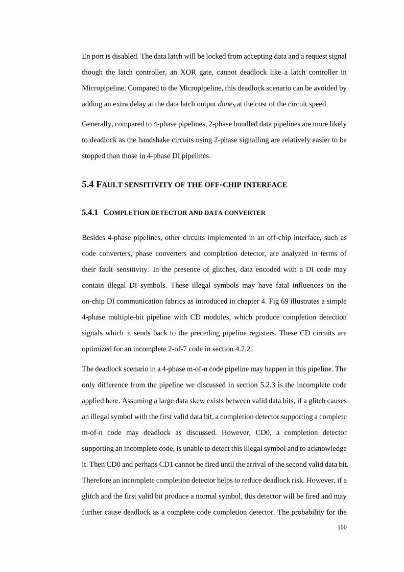
100
En port is disabled. The data latch will be locked from accepting data and a request signal
though the latch controller, an XOR gate, cannot deadlock like a latch controller in
Micropipeline. Compared to the Micropipeline, this deadlock scenario can be avoided by
adding an extra delay at the data latch output doneN at the cost of the circuit speed.
Generally, compared to 4-phase pipelines, 2-phase bundled data pipelines are more likely
to deadlock as the handshake circuits using 2-phase signalling are relatively easier to be
stopped than those in 4-phase DI pipelines.
5.4 FAULT SENSITIVITY OF THE OFF-CHIP INTERFACE
5.4.1 COMPLETION DETECTOR AND DATA CONVERTER
Besides 4-phase pipelines, other circuits implemented in an off-chip interface, such as
code converters, phase converters and completion detector, are analyzed in terms of
their fault sensitivity. In the presence of glitches, data encoded with a DI code may
contain illegal DI symbols. These illegal symbols may have fatal influences on the
on-chip DI communication fabrics as introduced in chapter 4. Fig 69 illustrates a simple
4-phase multiple-bit pipeline with CD modules, which produce completion detection
signals which it sends back to the preceding pipeline registers. These CD circuits are
optimized for an incomplete 2-of-7 code in section 4.2.2.
The deadlock scenario in a 4-phase m-of-n code pipeline may happen in this pipeline. The
only difference from the pipeline we discussed in section 5.2.3 is the incomplete code
applied here. Assuming a large data skew exists between valid data bits, if a glitch causes
an illegal symbol with the first valid data bit, a completion detector supporting a complete
m-of-n code may deadlock as discussed. However, CD0, a completion detector
supporting an incomplete code, is unable to detect this illegal symbol and to acknowledge
it. Then CD0 and perhaps CD1 cannot be fired until the arrival of the second valid data bit.
Therefore an incomplete completion detector helps to reduce deadlock risk. However, if a
glitch and the first valid bit produce a normal symbol, this detector will be fired and may
further cause deadlock as a complete code completion detector. The probability for the
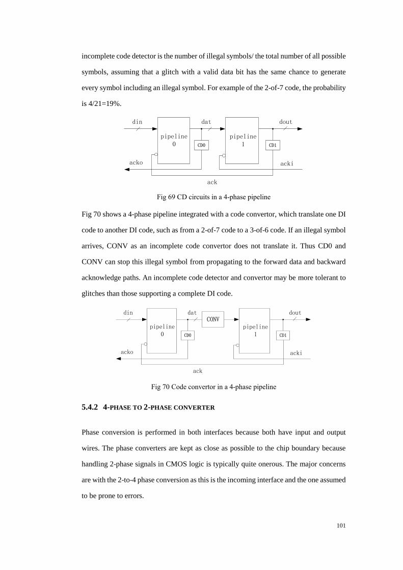
101
incomplete code detector is the number of illegal symbols/ the total number of all possible
symbols, assuming that a glitch with a valid data bit has the same chance to generate
every symbol including an illegal symbol. For example of the 2-of-7 code, the probability
is 4/21=19%.
CD0 CD1
pipeline0
din
pipeline1
doutdat
acki
ack
acko
Fig 69 CD circuits in a 4-phase pipeline
Fig 70 shows a 4-phase pipeline integrated with a code convertor, which translate one DI
code to another DI code, such as from a 2-of-7 code to a 3-of-6 code. If an illegal symbol
arrives, CONV as an incomplete code convertor does not translate it. Thus CD0 and
CONV can stop this illegal symbol from propagating to the forward data and backward
acknowledge paths. An incomplete code detector and convertor may be more tolerant to
glitches than those supporting a complete DI code.
CD0 CD1
pipeline0
din
pipeline1
doutdat
acki
ack
acko
CONV
Fig 70 Code convertor in a 4-phase pipeline
5.4.2 4-PHASE TO 2-PHASE CONVERTER
Phase conversion is performed in both interfaces because both have input and output
wires. The phase converters are kept as close as possible to the chip boundary because
handling 2-phase signals in CMOS logic is typically quite onerous. The major concerns
are with the 2-to-4 phase conversion as this is the incoming interface and the one assumed
to be prone to errors.
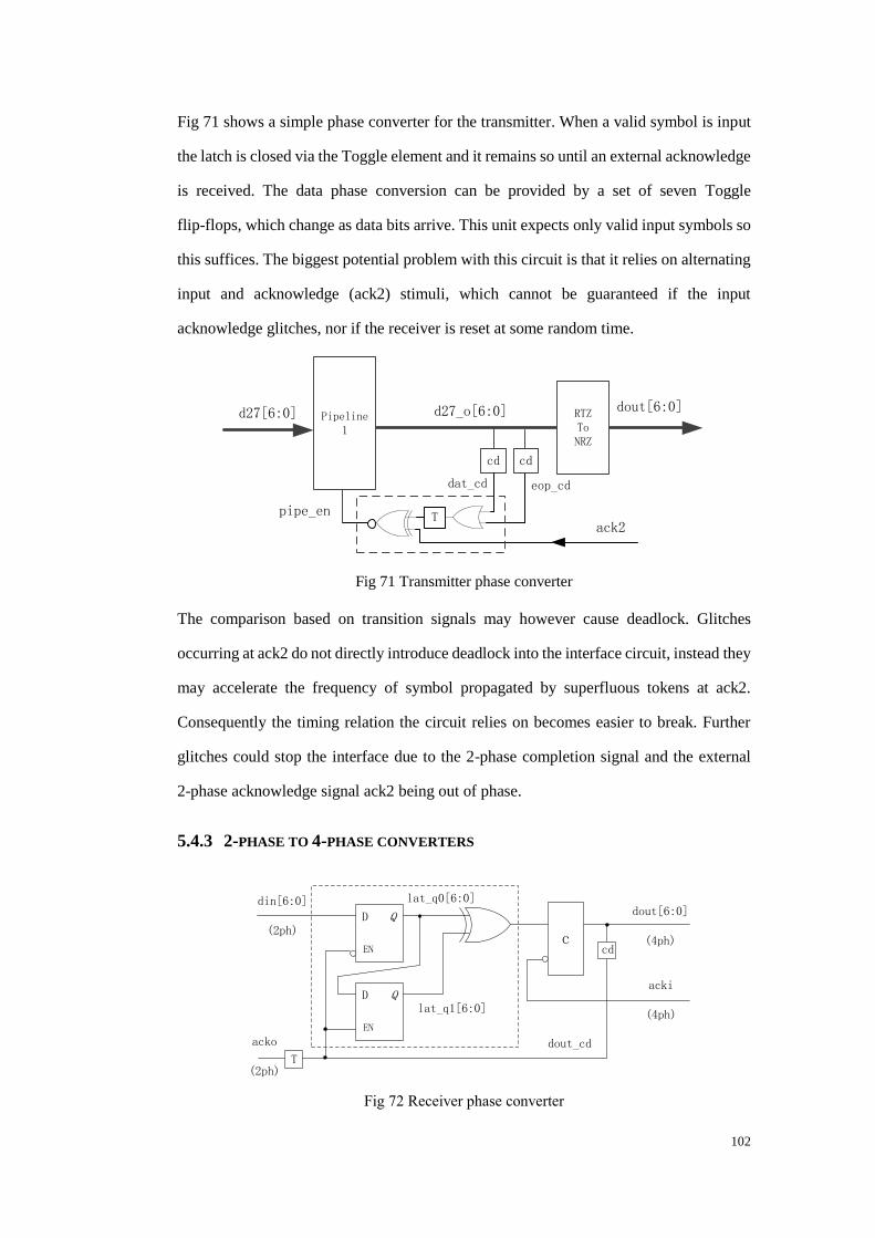
102
Fig 71 shows a simple phase converter for the transmitter. When a valid symbol is input
the latch is closed via the Toggle element and it remains so until an external acknowledge
is received. The data phase conversion can be provided by a set of seven Toggle
flip-flops, which change as data bits arrive. This unit expects only valid input symbols so
this suffices. The biggest potential problem with this circuit is that it relies on alternating
input and acknowledge (ack2) stimuli, which cannot be guaranteed if the input
acknowledge glitches, nor if the receiver is reset at some random time.
pipe_en
dout[6:0]Pipeline
1
ack2
cd cd
d27[6:0] RTZToNRZ
T
d27_o[6:0]
eop_cddat_cd
Fig 71 Transmitter phase converter
The comparison based on transition signals may however cause deadlock. Glitches
occurring at ack2 do not directly introduce deadlock into the interface circuit, instead they
may accelerate the frequency of symbol propagated by superfluous tokens at ack2.
Consequently the timing relation the circuit relies on becomes easier to break. Further
glitches could stop the interface due to the 2-phase completion signal and the external
2-phase acknowledge signal ack2 being out of phase.
5.4.3 2-PHASE TO 4-PHASE CONVERTERS
D
EN
Q
D
EN
Q
din[6:0]
(2ph)
lat_q0[6:0]
lat_q1[6:0]
cdc
T
acki
(4ph)
dout[6:0]
(4ph)
acko
(2ph)
dout_cd
Fig 72 Receiver phase converter
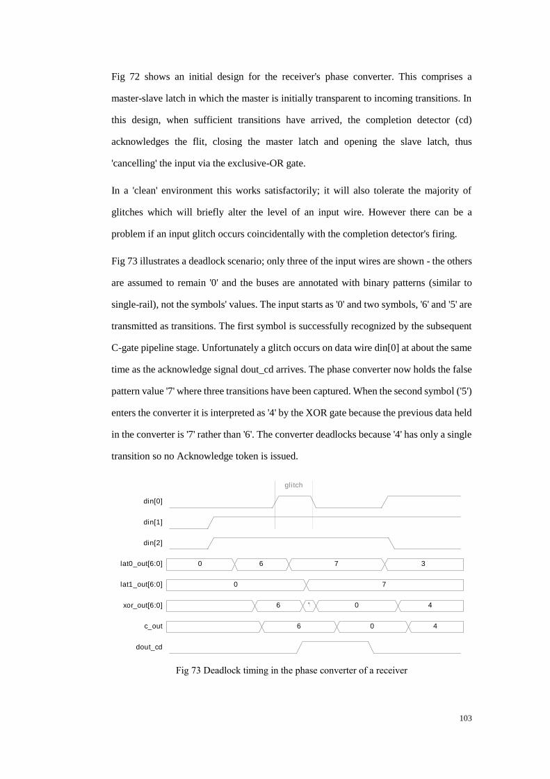
103
Fig 72 shows an initial design for the receiver's phase converter. This comprises a
master-slave latch in which the master is initially transparent to incoming transitions. In
this design, when sufficient transitions have arrived, the completion detector (cd)
acknowledges the flit, closing the master latch and opening the slave latch, thus
'cancelling' the input via the exclusive-OR gate.
In a 'clean' environment this works satisfactorily; it will also tolerate the majority of
glitches which will briefly alter the level of an input wire. However there can be a
problem if an input glitch occurs coincidentally with the completion detector's firing.
Fig 73 illustrates a deadlock scenario; only three of the input wires are shown - the others
are assumed to remain '0' and the buses are annotated with binary patterns (similar to
single-rail), not the symbols' values. The input starts as '0' and two symbols, '6' and '5' are
transmitted as transitions. The first symbol is successfully recognized by the subsequent
C-gate pipeline stage. Unfortunately a glitch occurs on data wire din[0] at about the same
time as the acknowledge signal dout_cd arrives. The phase converter now holds the false
pattern value '7' where three transitions have been captured. When the second symbol ('5')
enters the converter it is interpreted as '4' by the XOR gate because the previous data held
in the converter is '7' rather than '6'. The converter deadlocks because '4' has only a single
transition so no Acknowledge token is issued.
glitch
0 6 7 3
0 7
6 'H02 0 4
6 0 4
din[0]
din[1]
din[2]
lat0_out[6:0]
lat1_out[6:0]
xor_out[6:0]
c_out
dout_cd
Fig 73 Deadlock timing in the phase converter of a receiver
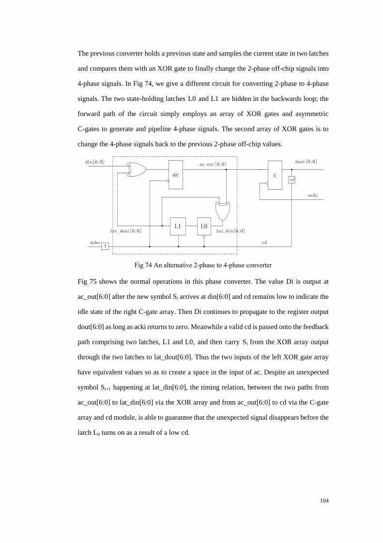
104
The previous converter holds a previous state and samples the current state in two latches
and compares them with an XOR gate to finally change the 2-phase off-chip signals into
4-phase signals. In Fig 74, we give a different circuit for converting 2-phase to 4-phase
signals. The two state-holding latches L0 and L1 are hidden in the backwards loop; the
forward path of the circuit simply employs an array of XOR gates and asymmetric
C-gates to generate and pipeline 4-phase signals. The second array of XOR gates is to
change the 4-phase signals back to the previous 2-phase off-chip values.
L1 L0
ac
din[6:0]
lat_din[6:0]lat_dout[6:0]
Tacko
c
acki
dout[6:0]
cd
cd
ac_out[6:0]
Fig 74 An alternative 2-phase to 4-phase converter
Fig 75 shows the normal operations in this phase converter. The value Di is output at
ac_out[6:0] after the new symbol Si arrives at din[6:0] and cd remains low to indicate the
idle state of the right C-gate array. Then Di continues to propagate to the register output
dout[6:0] as long as acki returns to zero. Meanwhile a valid cd is passed onto the feedback
path comprising two latches, L1 and L0, and then carry Si from the XOR array output
through the two latches to lat_dout[6:0]. Thus the two inputs of the left XOR gate array
have equivalent values so as to create a space in the input of ac. Despite an unexpected
symbol Si+1 happening at lat_din[6:0], the timing relation, between the two paths from
ac_out[6:0] to lat_din[6:0] via the XOR array and from ac_out[6:0] to cd via the C-gate
array and cd module, is able to guarantee that the unexpected signal disappears before the
latch L0 turns on as a result of a low cd.
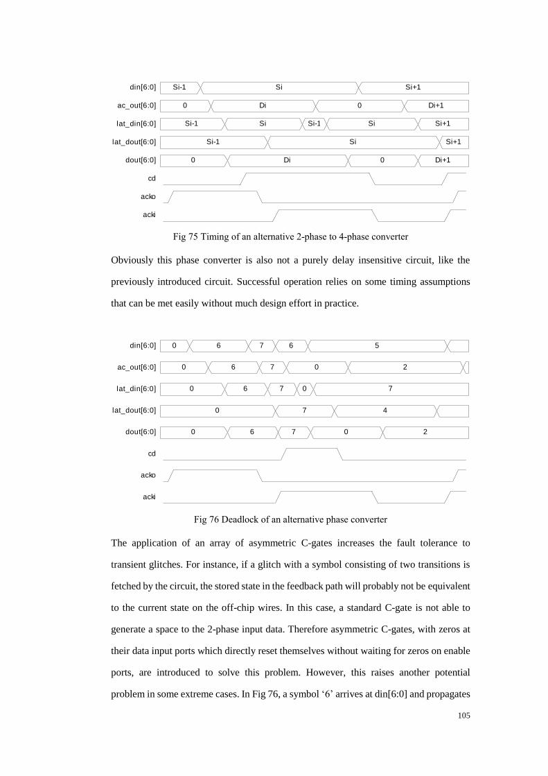
105
Si-1 Si Si+1
0 Di 0 Di+1
Si-1 Si Si-1 Si Si+1
Si-1 Si Si+1
0 Di 0 Di+1
din[6:0]
ac_out[6:0]
lat_din[6:0]
lat_dout[6:0]
dout[6:0]
cd
acko
acki
Fig 75 Timing of an alternative 2-phase to 4-phase converter
Obviously this phase converter is also not a purely delay insensitive circuit, like the
previously introduced circuit. Successful operation relies on some timing assumptions
that can be met easily without much design effort in practice.
0 6 7 6 5
0 6 7 0 2
0 6 7 0 7
0 7 4
0 6 7 0 2
din[6:0]
ac_out[6:0]
lat_din[6:0]
lat_dout[6:0]
dout[6:0]
cd
acko
acki
Fig 76 Deadlock of an alternative phase converter
The application of an array of asymmetric C-gates increases the fault tolerance to
transient glitches. For instance, if a glitch with a symbol consisting of two transitions is
fetched by the circuit, the stored state in the feedback path will probably not be equivalent
to the current state on the off-chip wires. In this case, a standard C-gate is not able to
generate a space to the 2-phase input data. Therefore asymmetric C-gates, with zeros at
their data input ports which directly reset themselves without waiting for zeros on enable
ports, are introduced to solve this problem. However, this raises another potential
problem in some extreme cases. In Fig 76, a symbol „6‟ arrives at din[6:0] and propagates
106
through ac_out[6:0] till dout[6:]. However, later a glitch changes din[6:0] from „6‟ into
„7‟ and also changes the stored state lat_dout[6:0] from „6‟ to „7‟. When the next 2-phase
2-of-7 symbol „5‟ arrives at din[6:0], XORing with lat_dout[6:0] which is a „7‟ rather
than „6‟ results „2‟ at ac_out[6:0] and later at dout[6:0]. „2‟ only contains one transition,
leading to deadlock in the receiver.
5.5 SUMMARY
C-gates investigated under the attack of a single transient fault. Their outputs may be
flipped as a result of a transient glitch in some sensitive states. 2-phase and 4-phase
pipeline circuits were also investigated. Deadlock may occur in the pipeline circuits due
to handshake failures. One exception is the 2-phase bundled-data Mouse-trap pipeline,
which is unlikely to deadlock due to the lack of C-gates in its control channels.
In the original design of the off-chip interface in SpiNNaker, transient glitches on the
off-chip wires may result in deadlock in the circuits. In the following chapters, two
approaches are proposed to address this deadlock issue.
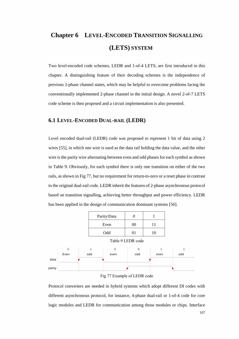
107
Chapter 6 LEVEL-ENCODED TRANSITION SIGNALLING
(LETS) SYSTEM
Two level-encoded code schemes, LEDR and 1-of-4 LETS, are first introduced in this
chapter. A distinguishing feature of their decoding schemes is the independence of
previous 2-phase channel states, which may be helpful to overcome problems facing the
conventionally implemented 2-phase channel in the initial design. A novel 2-of-7 LETS
code scheme is then proposed and a circuit implementation is also presented.
6.1 LEVEL-ENCODED DUAL-RAIL (LEDR)
Level encoded dual-rail (LEDR) code was proposed to represent 1 bit of data using 2
wires [55], in which one wire is used as the data rail holding the data value, and the other
wire is the parity wire alternating between even and odd phases for each symbol as shown
in Table 9. Obviously, for each symbol there is only one transition on either of the two
rails, as shown in Fig 77, but no requirement for return-to-zero or a reset phase in contrast
to the original dual-rail code. LEDR inherit the features of 2-phase asynchronous protocol
based on transition signalling, achieving better throughput and power efficiency. LEDR
has been applied in the design of communication dominant systems [56].
Parity\Data 0 1
Even 00 11
Odd 01 10
Table 9 LEDR code
0 1 0 0 1 1
Even odd even odd even odd
data
pari ty
Fig 77 Example of LEDR code
Protocol converters are needed in hybrid systems which adopt different DI codes with
different asynchronous protocol, for instance, 4-phase dual-rail or 1-of-4 code for core
logic modules and LEDR for communication among those modules or chips. Interface
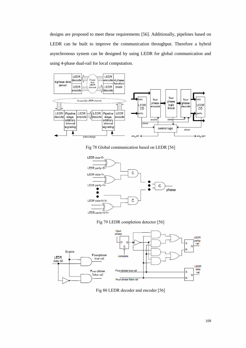
108
designs are proposed to meet these requirements [56]. Additionally, pipelines based on
LEDR can be built to improve the communication throughput. Therefore a hybrid
asynchronous system can be designed by using LEDR for global communication and
using 4-phase dual-rail for local computation.
Fig 78 Global communication based on LEDR [56]
Fig 79 LEDR completion detector [56]
Fig 80 LEDR decoder and encoder [56]
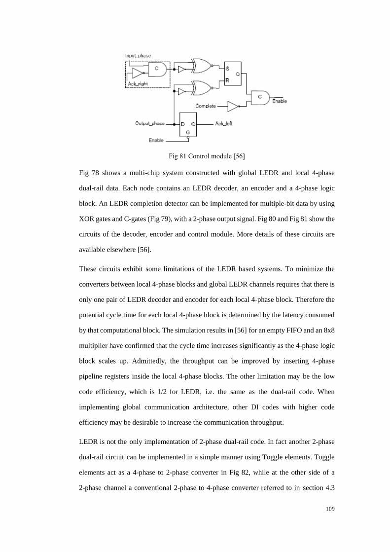
109
Fig 81 Control module [56]
Fig 78 shows a multi-chip system constructed with global LEDR and local 4-phase
dual-rail data. Each node contains an LEDR decoder, an encoder and a 4-phase logic
block. An LEDR completion detector can be implemented for multiple-bit data by using
XOR gates and C-gates (Fig 79), with a 2-phase output signal. Fig 80 and Fig 81 show the
circuits of the decoder, encoder and control module. More details of these circuits are
available elsewhere [56].
These circuits exhibit some limitations of the LEDR based systems. To minimize the
converters between local 4-phase blocks and global LEDR channels requires that there is
only one pair of LEDR decoder and encoder for each local 4-phase block. Therefore the
potential cycle time for each local 4-phase block is determined by the latency consumed
by that computational block. The simulation results in [56] for an empty FIFO and an 8x8
multiplier have confirmed that the cycle time increases significantly as the 4-phase logic
block scales up. Admittedly, the throughput can be improved by inserting 4-phase
pipeline registers inside the local 4-phase blocks. The other limitation may be the low
code efficiency, which is 1/2 for LEDR, i.e. the same as the dual-rail code. When
implementing global communication architecture, other DI codes with higher code
efficiency may be desirable to increase the communication throughput.
LEDR is not the only implementation of 2-phase dual-rail code. In fact another 2-phase
dual-rail circuit can be implemented in a simple manner using Toggle elements. Toggle
elements act as a 4-phase to 2-phase converter in Fig 82, while at the other side of a
2-phase channel a conventional 2-phase to 4-phase converter referred to in section 4.3
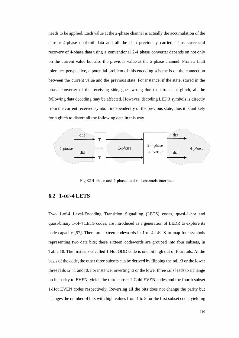
110
needs to be applied. Each value at the 2-phase channel is actually the accumulation of the
current 4-phase dual-rail data and all the data previously carried. Thus successful
recovery of 4-phase data using a conventional 2-4 phase converter depends on not only
on the current value but also the previous value at the 2-phase channel. From a fault
tolerance perspective, a potential problem of this encoding scheme is on the connection
between the current value and the previous state. For instance, if the state, stored in the
phase converter of the receiving side, goes wrong due to a transient glitch, all the
following data decoding may be affected. However, decoding LEDR symbols is directly
from the current received symbol, independently of the previous state, thus it is unlikely
for a glitch to distort all the following data in this way.
Fig 82 4-phase and 2-phase dual-rail channels interface
6.2 1-OF-4 LETS
Two 1-of-4 Level-Encoding Transition Signalling (LETS) codes, quasi-1-hot and
quasi-binary 1-of-4 LETS codes, are introduced as a generation of LEDR to explore its
code capacity [57]. There are sixteen codewords in 1-of-4 LETS to map four symbols
representing two data bits; these sixteen codewords are grouped into four subsets, in
Table 10. The first subset called 1-Hot ODD code is one bit high out of four rails. At the
basis of the code, the other three subsets can be derived by flipping the rail r3 or the lower
three rails r2, r1 and r0. For instance, inverting r3 or the lower three rails leads to a change
on its parity to EVEN, yields the third subset 1-Cold EVEN codes and the fourth subset
1-Hot EVEN codes respectively. Reversing all the bits does not change the parity but
changes the number of bits with high values from 1 to 3 for the first subset code, yielding
T
T
2-4 phase
converter dt.f
dt.t dr.t
dr.f 4-phase 4-phase 2-phase
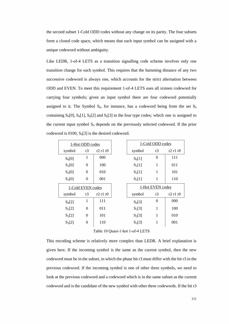
111
the second subset 1-Cold ODD codes without any change on its parity. The four subsets
form a closed code space, which means that each input symbol can be assigned with a
unique codeword without ambiguity.
Like LEDR, 1-of-4 LETS as a transition signalling code scheme involves only one
transition change for each symbol. This requires that the hamming distance of any two
successive codeword is always one, which accounts for the strict alternation between
ODD and EVEN. To meet this requirement 1-of-4 LETS uses all sixteen codeword for
carrying four symbols; given an input symbol there are four codeword potentially
assigned to it. The Symbol S0, for instance, has a codeword being from the set S0
containing S0[0], S0[1], S0[2] and S0[3] in the four type codes; which one is assigned to
the current input symbol S0 depends on the previously selected codeword. If the prior
codeword is 0100, S0[3] is the desired codeword.
1-Hot ODD codes 1-Cold ODD codes
symbol r3 r2 r1 r0 symbol r3 r2 r1 r0
S0[0] 1 000 S0[1] 0 111
S1[0] 0 100 S1[1] 1 011
S2[0] 0 010 S2[1] 1 101
S3[0] 0 001 S3[1] 1 110
1-Cold EVEN codes 1-Hot EVEN codes
symbol r3 r2 r1 r0 symbol r3 r2 r1 r0
S0[2] 1 111 S0[3] 0 000
S1[2] 0 011 S1[3] 1 100
S2[2] 0 101 S2[3] 1 010
S3[2] 0 110 S3[3] 1 001
Table 10 Quasi-1-hot 1-of-4 LETS
This encoding scheme is relatively more complex than LEDR. A brief explanation is
given here. If the incoming symbol is the same as the current symbol, then the new
codeword must be in the subset, in which the phase bit r3 must differ with the bit r3 in the
previous codeword. If the incoming symbol is one of other three symbols, we need to
look at the previous codeword and a codeword which is in the same subset as the current
codeword and is the candidate of the new symbol with other three codewords. If the bit r3
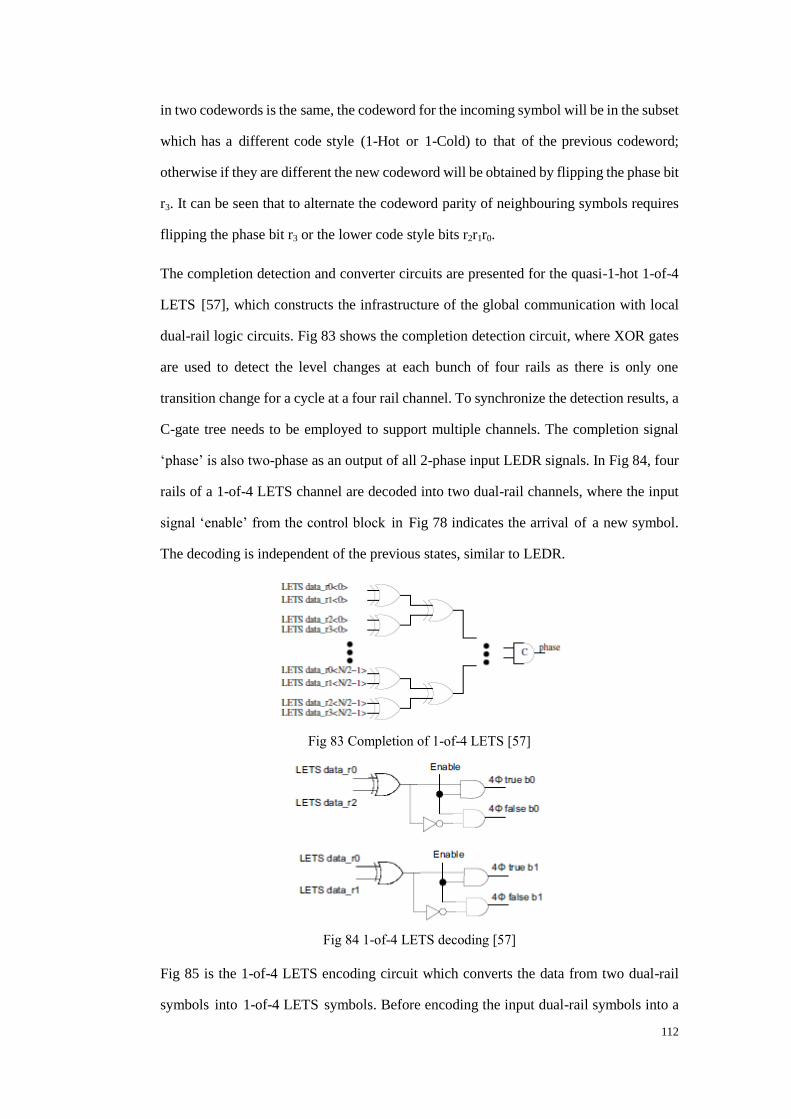
112
in two codewords is the same, the codeword for the incoming symbol will be in the subset
which has a different code style (1-Hot or 1-Cold) to that of the previous codeword;
otherwise if they are different the new codeword will be obtained by flipping the phase bit
r3. It can be seen that to alternate the codeword parity of neighbouring symbols requires
flipping the phase bit r3 or the lower code style bits r2r1r0.
The completion detection and converter circuits are presented for the quasi-1-hot 1-of-4
LETS [57], which constructs the infrastructure of the global communication with local
dual-rail logic circuits. Fig 83 shows the completion detection circuit, where XOR gates
are used to detect the level changes at each bunch of four rails as there is only one
transition change for a cycle at a four rail channel. To synchronize the detection results, a
C-gate tree needs to be employed to support multiple channels. The completion signal
„phase‟ is also two-phase as an output of all 2-phase input LEDR signals. In Fig 84, four
rails of a 1-of-4 LETS channel are decoded into two dual-rail channels, where the input
signal „enable‟ from the control block in Fig 78 indicates the arrival of a new symbol.
The decoding is independent of the previous states, similar to LEDR.
Fig 83 Completion of 1-of-4 LETS [57]
Fig 84 1-of-4 LETS decoding [57]
Fig 85 is the 1-of-4 LETS encoding circuit which converts the data from two dual-rail
symbols into 1-of-4 LETS symbols. Before encoding the input dual-rail symbols into a
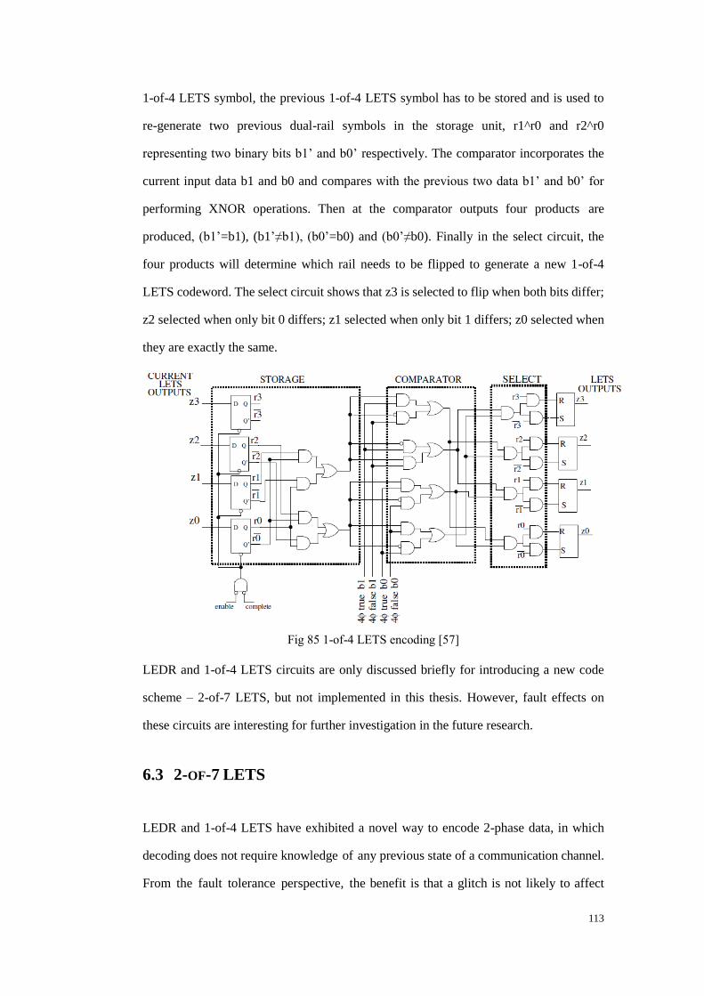
113
1-of-4 LETS symbol, the previous 1-of-4 LETS symbol has to be stored and is used to
re-generate two previous dual-rail symbols in the storage unit, r1^r0 and r2^r0
representing two binary bits b1‟ and b0‟ respectively. The comparator incorporates the
current input data b1 and b0 and compares with the previous two data b1‟ and b0‟ for
performing XNOR operations. Then at the comparator outputs four products are
produced, (b1‟=b1), (b1‟≠b1), (b0‟=b0) and (b0‟≠b0). Finally in the select circuit, the
four products will determine which rail needs to be flipped to generate a new 1-of-4
LETS codeword. The select circuit shows that z3 is selected to flip when both bits differ;
z2 selected when only bit 0 differs; z1 selected when only bit 1 differs; z0 selected when
they are exactly the same.
Fig 85 1-of-4 LETS encoding [57]
LEDR and 1-of-4 LETS circuits are only discussed briefly for introducing a new code
scheme – 2-of-7 LETS, but not implemented in this thesis. However, fault effects on
these circuits are interesting for further investigation in the future research.
6.3 2-OF-7 LETS
LEDR and 1-of-4 LETS have exhibited a novel way to encode 2-phase data, in which
decoding does not require knowledge of any previous state of a communication channel.
From the fault tolerance perspective, the benefit is that a glitch is not likely to affect
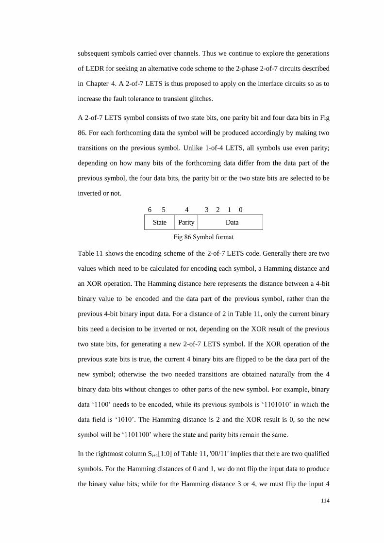
114
subsequent symbols carried over channels. Thus we continue to explore the generations
of LEDR for seeking an alternative code scheme to the 2-phase 2-of-7 circuits described
in Chapter 4. A 2-of-7 LETS is thus proposed to apply on the interface circuits so as to
increase the fault tolerance to transient glitches.
A 2-of-7 LETS symbol consists of two state bits, one parity bit and four data bits in Fig
86. For each forthcoming data the symbol will be produced accordingly by making two
transitions on the previous symbol. Unlike 1-of-4 LETS, all symbols use even parity;
depending on how many bits of the forthcoming data differ from the data part of the
previous symbol, the four data bits, the parity bit or the two state bits are selected to be
inverted or not.
6 5 4 3 2 1 0
State Parity Data
Fig 86 Symbol format
Table 11 shows the encoding scheme of the 2-of-7 LETS code. Generally there are two
values which need to be calculated for encoding each symbol, a Hamming distance and
an XOR operation. The Hamming distance here represents the distance between a 4-bit
binary value to be encoded and the data part of the previous symbol, rather than the
previous 4-bit binary input data. For a distance of 2 in Table 11, only the current binary
bits need a decision to be inverted or not, depending on the XOR result of the previous
two state bits, for generating a new 2-of-7 LETS symbol. If the XOR operation of the
previous state bits is true, the current 4 binary bits are flipped to be the data part of the
new symbol; otherwise the two needed transitions are obtained naturally from the 4
binary data bits without changes to other parts of the new symbol. For example, binary
data „1100‟ needs to be encoded, while its previous symbols is „1101010‟ in which the
data field is „1010‟. The Hamming distance is 2 and the XOR result is 0, so the new
symbol will be „1101100‟ where the state and parity bits remain the same.
In the rightmost column Si+1[1:0] of Table 11, '00/11' implies that there are two qualified
symbols. For the Hamming distances of 0 and 1, we do not flip the input data to produce
the binary value bits; while for the Hamming distance 3 or 4, we must flip the input 4
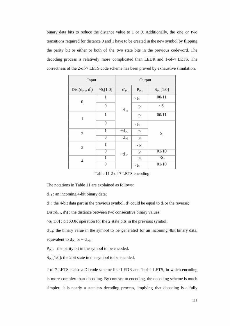
115
binary data bits to reduce the distance value to 1 or 0. Additionally, the one or two
transitions required for distance 0 and 1 have to be created in the new symbol by flipping
the parity bit or either or both of the two state bits in the previous codeword. The
decoding process is relatively more complicated than LEDR and 1-of-4 LETS. The
correctness of the 2-of-7 LETS code scheme has been proved by exhaustive simulation.
Input Output
Dist(di+1, d'i) ^Si[1:0] d'i+1 Pi+1 Si+1[1:0]
0 1
di+1
~ Pi 00/11
0 Pi ~Si
1 1 Pi 00/11
0 ~ Pi
Si 2 1 ~di+1 Pi
0 di+1 Pi
3 1
~di+1
~ Pi
0 Pi 01/10
4 1 Pi ~Si
0 ~ Pi 01/10
Table 11 2-of-7 LETS encoding
The notations in Table 11 are explained as follows:
di+1 : an incoming 4-bit binary data;
d'i : the 4-bit data part in the previous symbol, d'i could be equal to di or the reverse;
Dist(di+1, d'i) : the distance between two consecutive binary values;
^Si[1:0] : bit XOR operation for the 2 state bits in the previous symbol;
d'i+1: the binary value in the symbol to be generated for an incoming 4bit binary data,
equivalent to di+1 or ~ di+1;
Pi+1: the parity bit in the symbol to be encoded.
Si+1[1:0]: the 2bit state in the symbol to be encoded.
2-of-7 LETS is also a DI code scheme like LEDR and 1-of-4 LETS, in which encoding
is more complex than decoding. By contrast to encoding, the decoding scheme is much
simpler; it is nearly a stateless decoding process, implying that decoding is a fully
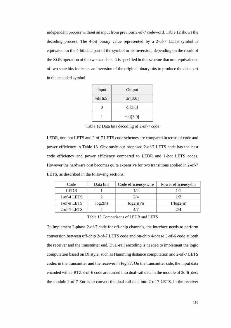
116
independent process without an input from previous 2-of-7 codeword. Table 12 shows the
decoding process. The 4-bit binary value represented by a 2-of-7 LETS symbol is
equivalent to the 4-bit data part of the symbol or its inversion, depending on the result of
the XOR operation of the two state bits. It is specified in this scheme that non-equivalence
of two state bits indicates an inversion of the original binary bits to produce the data part
in the encoded symbol.
Input Output
^di[6:5] di‟[3:0]
0 di[3:0]
1 ~di[3:0]
Table 12 Data bits decoding of 2-of-7 code
LEDR, one-hot LETS and 2-of-7 LETS code schemes are compared in terms of code and
power efficiency in Table 13. Obviously our proposed 2-of-7 LETS code has the best
code efficiency and power efficiency compared to LEDR and 1-hot LETS codes.
However the hardware cost becomes quite expensive for two transitions applied in 2-of-7
LETS, as described in the following sections.
Code Data bits Code efficiency/wire Power efficiency/bit
LEDR 1 1/2 1/1
1-of-4 LETS 2 2/4 1/2
1-of-n LETS log2(n) log2(n)/n 1/log2(n)
2-of-7 LETS 4 4/7 2/4
Table 13 Comparisons of LEDR and LETS
To implement 2-phase 2-of-7 code for off-chip channels, the interface needs to perform
conversion between off-chip 2-of-7 LETS code and on-chip 4-phase 3-of-6 code at both
the receiver and the transmitter end. Dual-rail encoding is needed to implement the logic
computation based on DI style, such as Hamming distance computation and 2-of-7 LETS
codec in the transmitter and the receiver in Fig 87. On the transmitter side, the input data
encoded with a RTZ 3-of-6 code are turned into dual-rail data in the module of 3of6_dec;
the module 2-of-7 Enc is to convert the dual-rail data into 2-of-7 LETS. In the receiver

117
side, the modules 2-of-7 Dec and 3-of-6 Enc convert the data from 2-of-7 LETS to
4-phase 3-of-6 via dual-rail data encoding in a reverse way.
d_1of2[7:0] d_27[6:0]d_36[5:0]d_36[5:0]
ack4
d_1of2[7:0]
4 phase 2 phase 4 phase
ack4
ack2
Transmitter Receiver
3-of-6
Enc
2-of-7
Dec
2-of-7
Enc
3-of-6
Dec
Fig 87 Off-chip interface using 2-of-7 LETS
Name Direction Description
d36[5:0] I Input data encoded with RTZ 3-of-6.
ctrl[2:0] I Control information bits.
ctrl[2]=1: EoP, ctrl[1] =1, gap; ctrl[0]=1, Normal. dat_ack O Acknowledge signal for the input data
ctrl_ack O Acknowledge signal for the 3 ctrl bits.
d27[6:0] O Output data encoded with NRZ 2of7.
ack2 I Acknowledge signal for the output data
Table 14 Transmitter Interface
Name Direction Description
d27[6:0] I Input data encoded with NRZ 2-of-7
ack2 O Acknowledge signal for the input data
d36[5:0] O Output data encoded with RTZ 3-of-6
ctrl[2:0] O Output ctrl bits encoded with RTZ one-hot.
dat_ack I Acknowledge signal for the output data
ctrl_ack I Acknowledge signal for the ctrl bits.
Table 15 Receiver Interface
In the rest of this chapter, we only consider the data channel for implementing 2-of-7
LETS in Fig 87, Table 14 and Table 15. Even when the control information such as EoP is
concerned, for simplicity it is assumed that an EoP arrives serially as the last symbol
within a packet. In order to implement the same interface as specified in chapter 4 a
serializer and a deserializer are needed in the transmitter and receiver respectively.
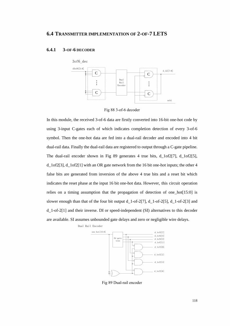
118
6.4 TRANSMITTER IMPLEMENTATION OF 2-OF-7 LETS
6.4.1 3-OF-6 DECODER
C
C
C
C
DualRail
Encoder
3of6_dec
d3of6[5:0]d_12[7:0]
acki
Fig 88 3-of-6 decoder
In this module, the received 3-of-6 data are firstly converted into 16-bit one-hot code by
using 3-input C-gates each of which indicates completion detection of every 3-of-6
symbol. Then the one-hot data are fed into a dual-rail decoder and encoded into 4 bit
dual-rail data. Finally the dual-rail data are registered to output through a C-gate pipeline.
The dual-rail encoder shown in Fig 89 generates 4 true bits, d_1of2[7], d_1of2[5],
d_1of2[3], d_1of2[1] with an OR gate network from the 16 bit one-hot inputs; the other 4
false bits are generated from inversion of the above 4 true bits and a reset bit which
indicates the reset phase at the input 16 bit one-hot data. However, this circuit operation
relies on a timing assumption that the propagation of detection of one_hot[15:0] is
slower enough than that of the four bit output d_1-of-2[7], d_1-of-2[5], d_1-of-2[3] and
d_1-of-2[1] and their inverse. DI or speed-independent (SI) alternatives to this decoder
are available. SI assumes unbounded gate delays and zero or negligible wire delays.
d_1of2[7]
d_1of2[5]
d_1of2[3]
d_1of2[1]
Or-gatetree
d_1of2[6]
d_1of2[4]
d_1of2[2]
d_1of2[0]
one_hot[15:0]
Dual Rail Encoder
Fig 89 Dual-rail encoder
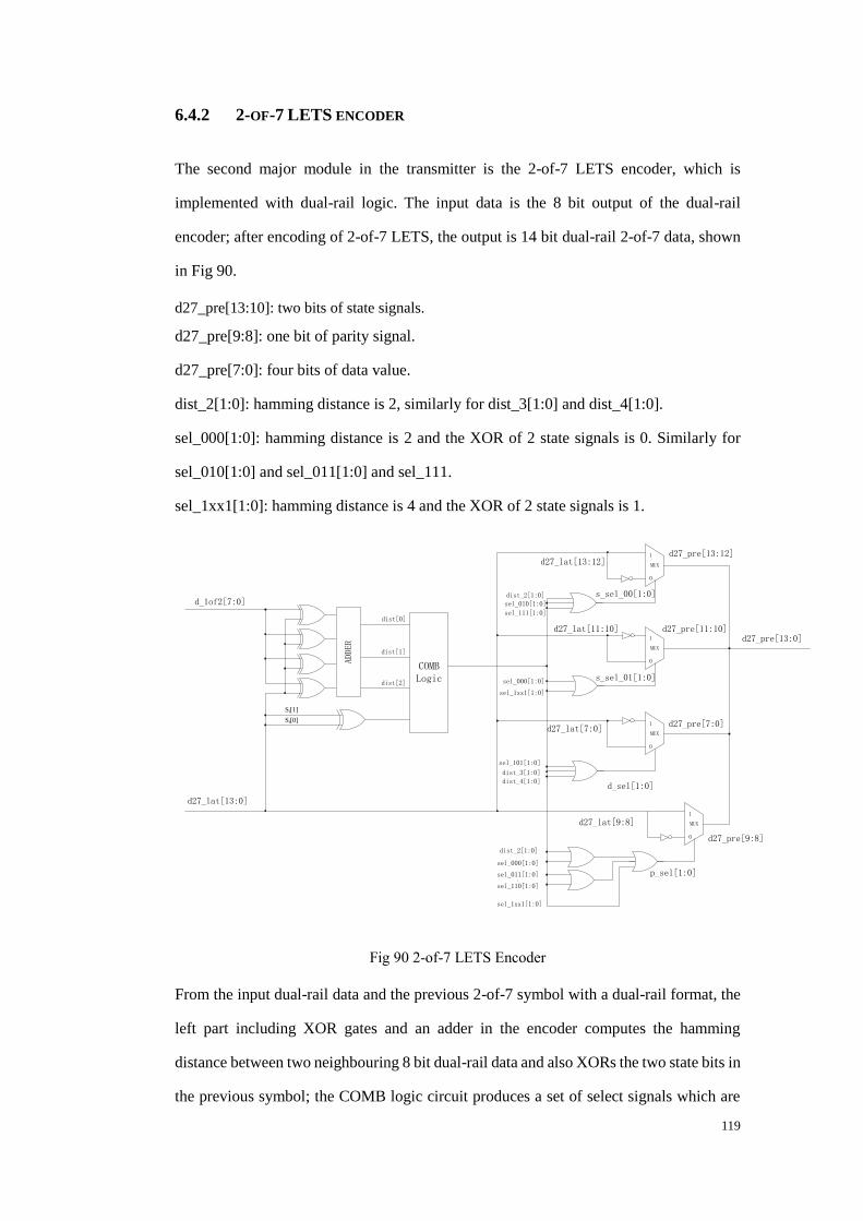
119
6.4.2 2-OF-7 LETS ENCODER
The second major module in the transmitter is the 2-of-7 LETS encoder, which is
implemented with dual-rail logic. The input data is the 8 bit output of the dual-rail
encoder; after encoding of 2-of-7 LETS, the output is 14 bit dual-rail 2-of-7 data, shown
in Fig 90.
d27_pre[13:10]: two bits of state signals.
d27_pre[9:8]: one bit of parity signal.
d27_pre[7:0]: four bits of data value.
dist_2[1:0]: hamming distance is 2, similarly for dist_3[1:0] and dist_4[1:0].
sel_000[1:0]: hamming distance is 2 and the XOR of 2 state signals is 0. Similarly for
sel_010[1:0] and sel_011[1:0] and sel_111.
sel_1xx1[1:0]: hamming distance is 4 and the XOR of 2 state signals is 1.
dist[0]
dist[1]
dist[2]
ADDER
Si[1]
Si[0]
MUXd27_lat[13:12]d27_pre[13:12]
s_sel_00[1:0]
0
1
MUX
d27_lat[11:10] d27_pre[11:10]
s_sel_01[1:0]
0
1
sel_010[1:0]
sel_111[1:0]
dist_2[1:0]
sel_000[1:0]
sel_1xx1[1:0]
MUXd27_lat[7:0]
d27_pre[7:0]
d_sel[1:0]
0
1
sel_101[1:0]
dist_3[1:0]
dist_4[1:0]
COMBLogic
MUXd27_lat[9:8]
d27_pre[9:8]
p_sel[1:0]
0
1
dist_2[1:0]
sel_000[1:0]
sel_011[1:0]
sel_110[1:0]
sel_1xx1[1:0]
d27_lat[13:0]
d_1of2[7:0]
d27_pre[13:0]
Fig 90 2-of-7 LETS Encoder
From the input dual-rail data and the previous 2-of-7 symbol with a dual-rail format, the
left part including XOR gates and an adder in the encoder computes the hamming
distance between two neighbouring 8 bit dual-rail data and also XORs the two state bits in
the previous symbol; the COMB logic circuit produces a set of select signals which are
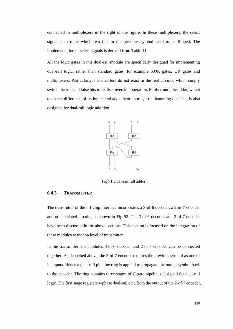
120
connected to multiplexers in the right of the figure. In these multiplexers, the select
signals determine which two bits in the previous symbol need to be flipped. The
implementation of select signals is derived from Table 11.
All the logic gates in this dual-rail module are specifically designed for implementing
dual-rail logic, rather than standard gates, for example XOR gates, OR gates and
multiplexers. Particularly, the inverters do not exist in the real circuits, which simply
switch the true and false bits to realise inversion operation. Furthermore the adder, which
takes the difference of its inputs and adds them up to get the hamming distance, is also
designed for dual-rail logic addition.
HA HA
FA HA
abcd
s0s1c
Fig 91 Dual-rail full adder
6.4.3 TRANSMITTER
The transmitter of the off-chip interface incorporates a 3-of-6 decoder, a 2-of-7 encoder
and other related circuits, as shown in Fig 92. The 3-of-6 decoder and 2-of-7 encoder
have been discussed in the above sections. This section is focused on the integration of
these modules at the top level of transmitter.
In the transmitter, the modules 3-of-6 decoder and 2-of-7 encoder can be connected
together. As described above, the 2-of-7 encoder requires the previous symbol as one of
its inputs. Hence a dual-rail pipeline ring is applied to propagate the output symbol back
to the encoder. The ring contains three stages of C-gate pipelines designed for dual-rail
logic. The first stage registers 4-phase dual-rail data from the output of the 2-of-7 encoder,
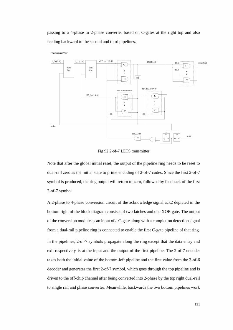
121
passing to a 4-phase to 2-phase converter based on C-gates at the right top and also
feeding backward to the second and third pipelines.
C
C
d_12[7:0]dout[6:0]
Transmitter
Cb0.t
b0.f
C
C
C
d27[13:0]
acko
cd
D
EN
Q D
EN
Q
ack2
C
C
d27_lat[13:0]
d27_pre[13:0]
ack2_4ph
d27_lat_pre[6:0]
C
cd
Reset to dual-rail zero
3of6
Dec
d_36[5:0]
2of7
Enc
cd
Fig 92 2-of-7 LETS transmitter
Note that after the global initial reset, the output of the pipeline ring needs to be reset to
dual-rail zero as the initial state to prime encoding of 2-of-7 codes. Since the first 2-of-7
symbol is produced, the ring output will return to zero, followed by feedback of the first
2-of-7 symbol.
A 2-phase to 4-phase conversion circuit of the acknowledge signal ack2 depicted in the
bottom right of the block diagram consists of two latches and one XOR gate. The output
of the conversion module as an input of a C-gate along with a completion detection signal
from a dual-rail pipeline ring is connected to enable the first C-gate pipeline of that ring.
In the pipelines, 2-of-7 symbols propagate along the ring except that the data entry and
exit respectively is at the input and the output of the first pipeline. The 2-of-7 encoder
takes both the initial value of the bottom-left pipeline and the first value from the 3-of-6
decoder and generates the first 2-of-7 symbol, which goes through the top pipeline and is
driven to the off-chip channel after being converted into 2-phase by the top right dual-rail
to single rail and phase converter. Meanwhile, backwards the two bottom pipelines work
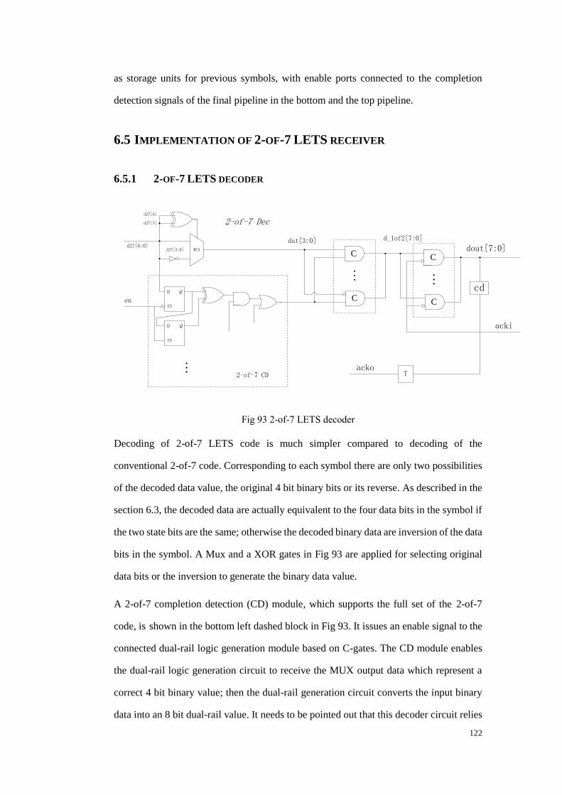
122
as storage units for previous symbols, with enable ports connected to the completion
detection signals of the final pipeline in the bottom and the top pipeline.
6.5 IMPLEMENTATION OF 2-OF-7 LETS RECEIVER
6.5.1 2-OF-7 LETS DECODER
D
EN
Q
D
EN
Q
MUX
d27[6]
d27[5]
d27[3:0]d27[6:0]
en
dat[3:0]
2-of-7 Dec
C
C
C
C
cd
acko
dout[7:0]
acki
T2-of-7 CD
d_1of2[7:0]
Fig 93 2-of-7 LETS decoder
Decoding of 2-of-7 LETS code is much simpler compared to decoding of the
conventional 2-of-7 code. Corresponding to each symbol there are only two possibilities
of the decoded data value, the original 4 bit binary bits or its reverse. As described in the
section 6.3, the decoded data are actually equivalent to the four data bits in the symbol if
the two state bits are the same; otherwise the decoded binary data are inversion of the data
bits in the symbol. A Mux and a XOR gates in Fig 93 are applied for selecting original
data bits or the inversion to generate the binary data value.
A 2-of-7 completion detection (CD) module, which supports the full set of the 2-of-7
code, is shown in the bottom left dashed block in Fig 93. It issues an enable signal to the
connected dual-rail logic generation module based on C-gates. The CD module enables
the dual-rail logic generation circuit to receive the MUX output data which represent a
correct 4 bit binary value; then the dual-rail generation circuit converts the input binary
data into an 8 bit dual-rail value. It needs to be pointed out that this decoder circuit relies
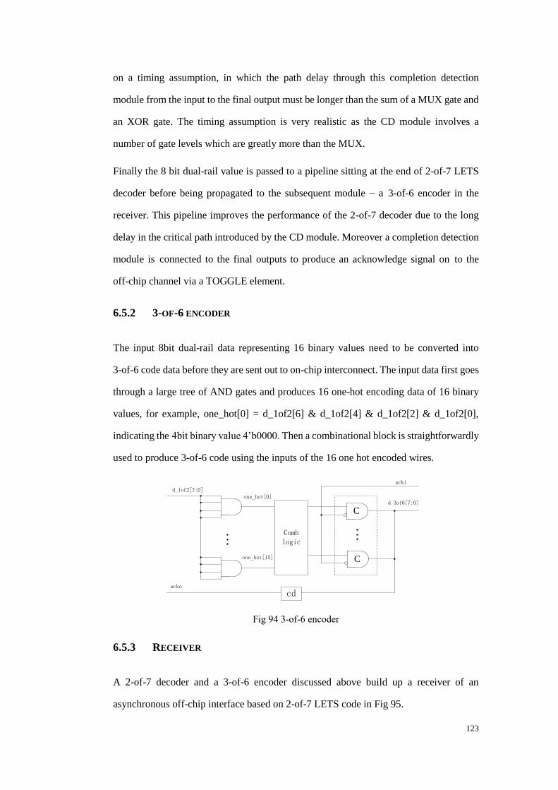
123
on a timing assumption, in which the path delay through this completion detection
module from the input to the final output must be longer than the sum of a MUX gate and
an XOR gate. The timing assumption is very realistic as the CD module involves a
number of gate levels which are greatly more than the MUX.
Finally the 8 bit dual-rail value is passed to a pipeline sitting at the end of 2-of-7 LETS
decoder before being propagated to the subsequent module – a 3-of-6 encoder in the
receiver. This pipeline improves the performance of the 2-of-7 decoder due to the long
delay in the critical path introduced by the CD module. Moreover a completion detection
module is connected to the final outputs to produce an acknowledge signal on to the
off-chip channel via a TOGGLE element.
6.5.2 3-OF-6 ENCODER
The input 8bit dual-rail data representing 16 binary values need to be converted into
3-of-6 code data before they are sent out to on-chip interconnect. The input data first goes
through a large tree of AND gates and produces 16 one-hot encoding data of 16 binary
values, for example, one_hot[0] = d_1of2[6] & d_1of2[4] & d_1of2[2] & d_1of2[0],
indicating the 4bit binary value 4‟b0000. Then a combinational block is straightforwardly
used to produce 3-of-6 code using the inputs of the 16 one hot encoded wires.
C
C
Comblogic
d_1of2[7:0]
d_3of6[7:0]
acki
one_hot[0]
one_hot[15]
cdacko
Fig 94 3-of-6 encoder
6.5.3 RECEIVER
A 2-of-7 decoder and a 3-of-6 encoder discussed above build up a receiver of an
asynchronous off-chip interface based on 2-of-7 LETS code in Fig 95.
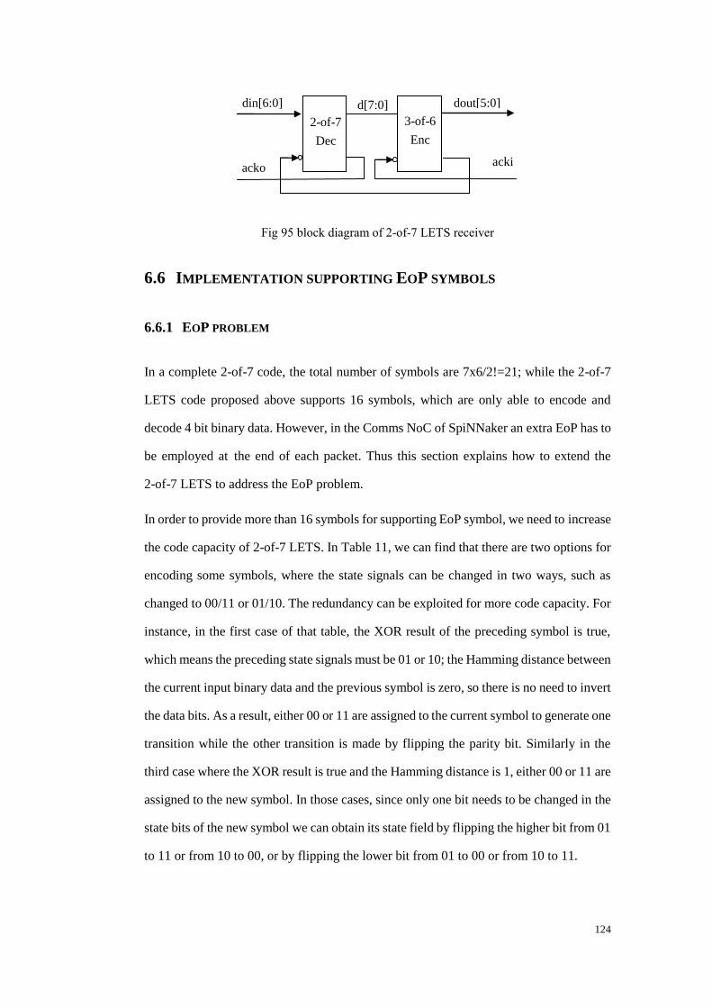
124
Fig 95 block diagram of 2-of-7 LETS receiver
6.6 IMPLEMENTATION SUPPORTING EOP SYMBOLS
6.6.1 EOP PROBLEM
In a complete 2-of-7 code, the total number of symbols are 7x6/2!=21; while the 2-of-7
LETS code proposed above supports 16 symbols, which are only able to encode and
decode 4 bit binary data. However, in the Comms NoC of SpiNNaker an extra EoP has to
be employed at the end of each packet. Thus this section explains how to extend the
2-of-7 LETS to address the EoP problem.
In order to provide more than 16 symbols for supporting EoP symbol, we need to increase
the code capacity of 2-of-7 LETS. In Table 11, we can find that there are two options for
encoding some symbols, where the state signals can be changed in two ways, such as
changed to 00/11 or 01/10. The redundancy can be exploited for more code capacity. For
instance, in the first case of that table, the XOR result of the preceding symbol is true,
which means the preceding state signals must be 01 or 10; the Hamming distance between
the current input binary data and the previous symbol is zero, so there is no need to invert
the data bits. As a result, either 00 or 11 are assigned to the current symbol to generate one
transition while the other transition is made by flipping the parity bit. Similarly in the
third case where the XOR result is true and the Hamming distance is 1, either 00 or 11 are
assigned to the new symbol. In those cases, since only one bit needs to be changed in the
state bits of the new symbol we can obtain its state field by flipping the higher bit from 01
to 11 or from 10 to 00, or by flipping the lower bit from 01 to 00 or from 10 to 11.
2-of-7
Dec
3-of-6
Enc
din[6:0] dout[5:0]
acko acki
d[7:0]
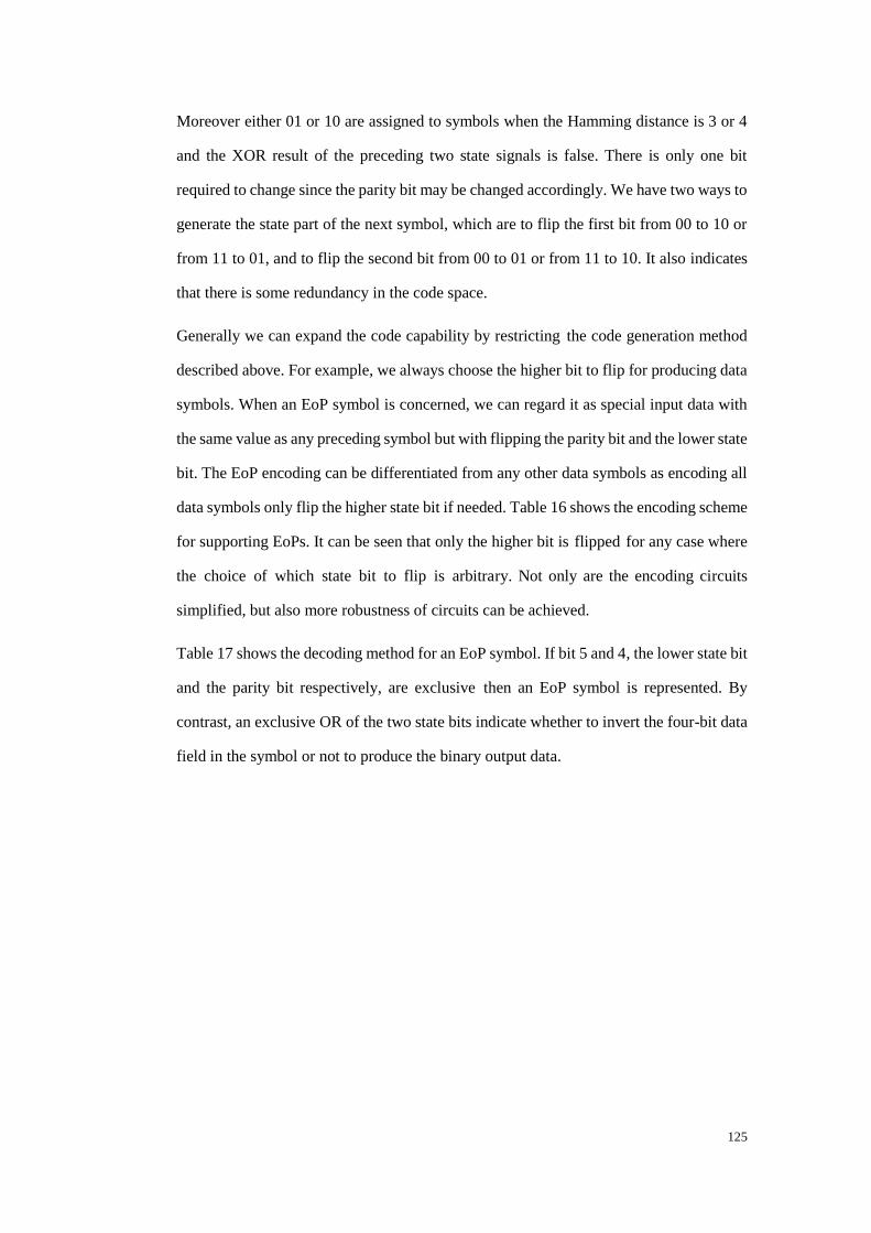
125
Moreover either 01 or 10 are assigned to symbols when the Hamming distance is 3 or 4
and the XOR result of the preceding two state signals is false. There is only one bit
required to change since the parity bit may be changed accordingly. We have two ways to
generate the state part of the next symbol, which are to flip the first bit from 00 to 10 or
from 11 to 01, and to flip the second bit from 00 to 01 or from 11 to 10. It also indicates
that there is some redundancy in the code space.
Generally we can expand the code capability by restricting the code generation method
described above. For example, we always choose the higher bit to flip for producing data
symbols. When an EoP symbol is concerned, we can regard it as special input data with
the same value as any preceding symbol but with flipping the parity bit and the lower state
bit. The EoP encoding can be differentiated from any other data symbols as encoding all
data symbols only flip the higher state bit if needed. Table 16 shows the encoding scheme
for supporting EoPs. It can be seen that only the higher bit is flipped for any case where
the choice of which state bit to flip is arbitrary. Not only are the encoding circuits
simplified, but also more robustness of circuits can be achieved.
Table 17 shows the decoding method for an EoP symbol. If bit 5 and 4, the lower state bit
and the parity bit respectively, are exclusive then an EoP symbol is represented. By
contrast, an exclusive OR of the two state bits indicate whether to invert the four-bit data
field in the symbol or not to produce the binary output data.
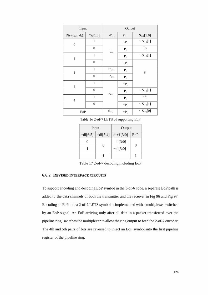
126
Input Output
Dist(di+1, d'i) ^Si[1:0] d'i+1 Pi+1 Si+1[1:0]
0 1
di+1
~Pi ~ Si+1[1]
0 Pi ~Si
1 1 Pi
~ Si+1[1]
0 ~Pi
Si 2 1 ~di+1 Pi
0 di+1 Pi
3 1
~di+1
~Pi
0 Pi ~ Si+1[1]
4 1 Pi
~Si
0 ~Pi ~ Si+1[1]
EoP di+1 ~Pi ~ Si+1[0]
Table 16 2-of-7 LETS of supporting EoP
Input Output
^di[6:5] ^di[5:4] di+1[3:0] EoP
0 0
di[3:0] 0
1 ~di[3:0]
1 1
Table 17 2-of-7 decoding including EoP
6.6.2 REVISED INTERFACE CIRCUITS
To support encoding and decoding EoP symbol in the 3-of-6 code, a separate EoP path is
added to the data channels of both the transmitter and the receiver in Fig 96 and Fig 97.
Encoding an EoP into a 2-of-7 LETS symbol is implemented with a multiplexer switched
by an EoP signal. An EoP arriving only after all data in a packet transferred over the
pipeline ring, switches the multiplexer to allow the ring output to feed the 2-of-7 encoder.
The 4th and 5th pairs of bits are reversed to inject an EoP symbol into the first pipeline
register of the pipeline ring.
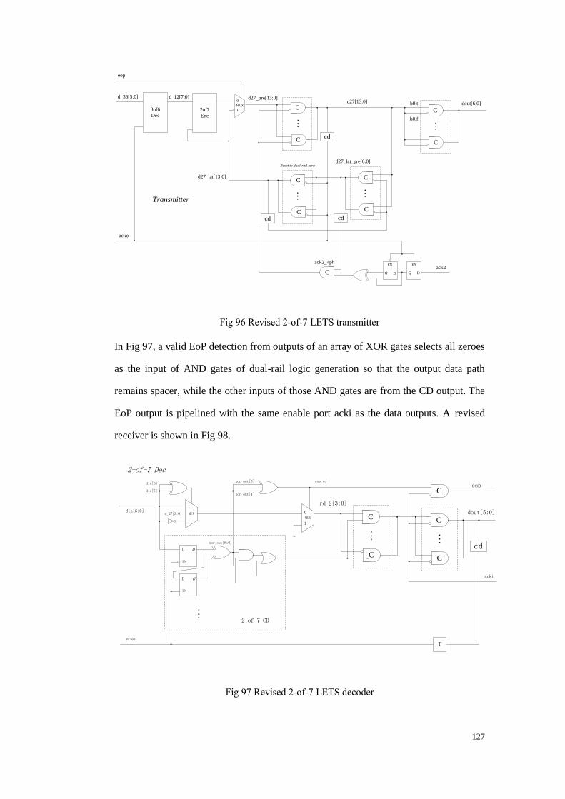
127
C
C
d_12[7:0]
dout[6:0]
Transmitter
Cb0.t
b0.f
C
C
C
d27[13:0]
acko
cd
D
EN
Q D
EN
Q
ack2
C
C
d27_lat[13:0]
d27_pre[13:0]
ack2_4ph
d27_lat_pre[6:0]
2of7
Enc
C
cd
Reset to dual-rail zero
MUX
eop
0
13of6
Dec
d_36[5:0]
cd
Fig 96 Revised 2-of-7 LETS transmitter
In Fig 97, a valid EoP detection from outputs of an array of XOR gates selects all zeroes
as the input of AND gates of dual-rail logic generation so that the output data path
remains spacer, while the other inputs of those AND gates are from the CD output. The
EoP output is pipelined with the same enable port acki as the data outputs. A revised
receiver is shown in Fig 98.
MUX
din[6]
din[5]
d_27[3:0]din[6:0]
rd_2[3:0]
2-of-7 Dec
C
C
C
C
cd
acki
T
-
-
acko
0
1
MUX
xor_out[5]
xor_out[4]
eop_cd
Ceop
dout[5:0]
D
EN
Q
D
EN
Q
2-of-7 CD
xor_out[6:0]
Fig 97 Revised 2-of-7 LETS decoder
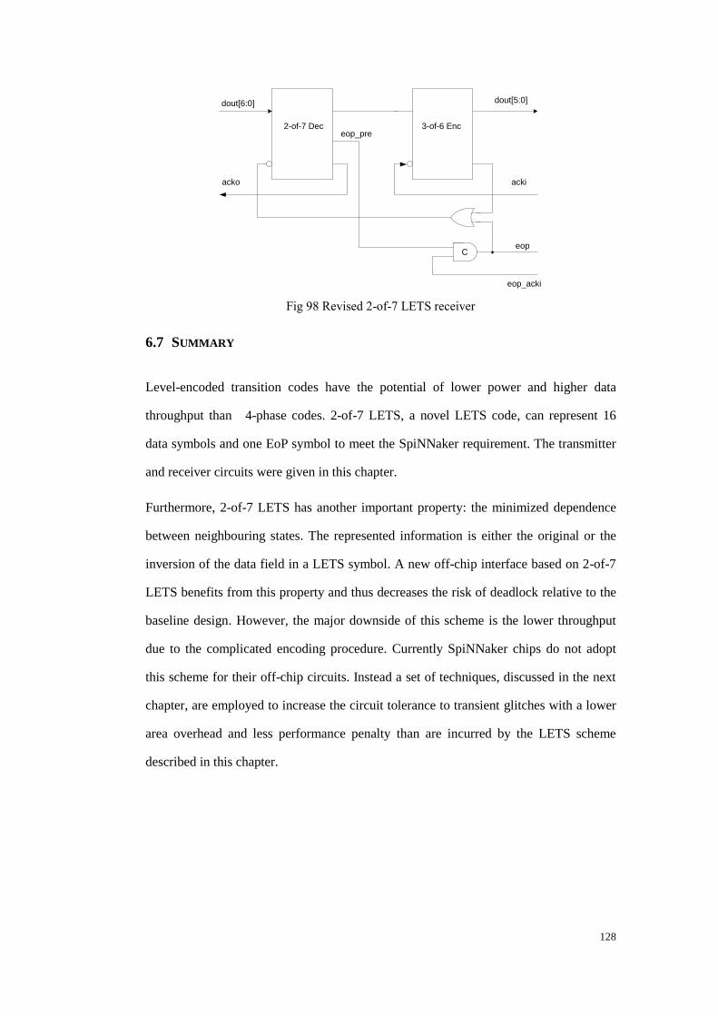
128
2-of-7 Dec 3-of-6 Enc
C
eop_acki
acki
eop
dout[5:0]dout[6:0]
eop_pre
acko
Fig 98 Revised 2-of-7 LETS receiver
6.7 SUMMARY
Level-encoded transition codes have the potential of lower power and higher data
throughput than 4-phase codes. 2-of-7 LETS, a novel LETS code, can represent 16
data symbols and one EoP symbol to meet the SpiNNaker requirement. The transmitter
and receiver circuits were given in this chapter.
Furthermore, 2-of-7 LETS has another important property: the minimized dependence
between neighbouring states. The represented information is either the original or the
inversion of the data field in a LETS symbol. A new off-chip interface based on 2-of-7
LETS benefits from this property and thus decreases the risk of deadlock relative to the
baseline design. However, the major downside of this scheme is the lower throughput
due to the complicated encoding procedure. Currently SpiNNaker chips do not adopt
this scheme for their off-chip circuits. Instead a set of techniques, discussed in the next
chapter, are employed to increase the circuit tolerance to transient glitches with a lower
area overhead and less performance penalty than are incurred by the LETS scheme
described in this chapter.
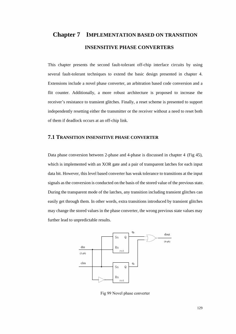
129
Chapter 7 IMPLEMENTATION BASED ON TRANSITION
INSENSITIVE PHASE CONVERTERS
This chapter presents the second fault-tolerant off-chip interface circuits by using
several fault-tolerant techniques to extend the basic design presented in chapter 4.
Extensions include a novel phase converter, an arbitration based code conversion and a
flit counter. Additionally, a more robust architecture is proposed to increase the
receiver‟s resistance to transient glitches. Finally, a reset scheme is presented to support
independently resetting either the transmitter or the receiver without a need to reset both
of them if deadlock occurs at an off-chip link.
7.1 TRANSITION INSENSITIVE PHASE CONVERTER
Data phase conversion between 2-phase and 4-phase is discussed in chapter 4 (Fig 45),
which is implemented with an XOR gate and a pair of transparent latches for each input
data bit. However, this level based converter has weak tolerance to transitions at the input
signals as the conversion is conducted on the basis of the stored value of the previous state.
During the transparent mode of the latches, any transition including transient glitches can
easily get through them. In other words, extra transitions introduced by transient glitches
may change the stored values in the phase converter, the wrong previous state values may
further lead to unpredictable results.
clrn
din
(2-ph)
dout
(4-ph)
q0
q1
Sn
Rn
Q
rst
Sn
Rn
Q
rst
Fig 99 Novel phase converter
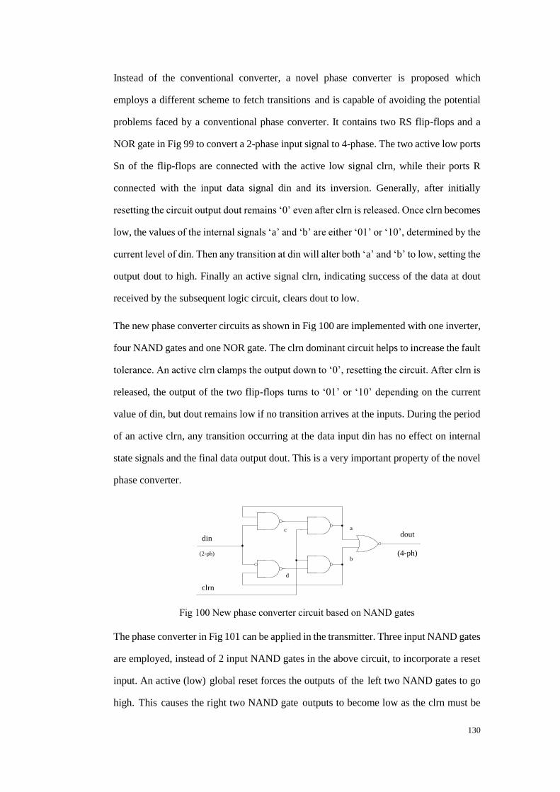
130
Instead of the conventional converter, a novel phase converter is proposed which
employs a different scheme to fetch transitions and is capable of avoiding the potential
problems faced by a conventional phase converter. It contains two RS flip-flops and a
NOR gate in Fig 99 to convert a 2-phase input signal to 4-phase. The two active low ports
Sn of the flip-flops are connected with the active low signal clrn, while their ports R
connected with the input data signal din and its inversion. Generally, after initially
resetting the circuit output dout remains „0‟ even after clrn is released. Once clrn becomes
low, the values of the internal signals „a‟ and „b‟ are either „01‟ or „10‟, determined by the
current level of din. Then any transition at din will alter both „a‟ and „b‟ to low, setting the
output dout to high. Finally an active signal clrn, indicating success of the data at dout
received by the subsequent logic circuit, clears dout to low.
The new phase converter circuits as shown in Fig 100 are implemented with one inverter,
four NAND gates and one NOR gate. The clrn dominant circuit helps to increase the fault
tolerance. An active clrn clamps the output down to „0‟, resetting the circuit. After clrn is
released, the output of the two flip-flops turns to „01‟ or „10‟ depending on the current
value of din, but dout remains low if no transition arrives at the inputs. During the period
of an active clrn, any transition occurring at the data input din has no effect on internal
state signals and the final data output dout. This is a very important property of the novel
phase converter.
dout
(4-ph)
a
b
clrn
din
(2-ph)
c
d
Fig 100 New phase converter circuit based on NAND gates
The phase converter in Fig 101 can be applied in the transmitter. Three input NAND gates
are employed, instead of 2 input NAND gates in the above circuit, to incorporate a reset
input. An active (low) global reset forces the outputs of the left two NAND gates to go
high. This causes the right two NAND gate outputs to become low as the clrn must be
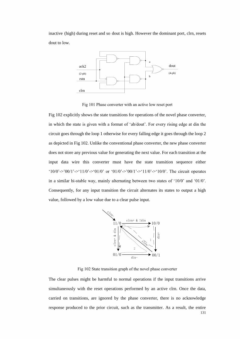
131
inactive (high) during reset and so dout is high. However the dominant port, clrn, resets
dout to low.
a
brstn
clrn
dout
(4-ph)
ack2
(2-ph)
Fig 101 Phase converter with an active low reset port
Fig 102 explicitly shows the state transitions for operations of the novel phase converter,
in which the state is given with a format of „ab/dout‟. For every rising edge at din the
circuit goes through the loop 1 otherwise for every falling edge it goes through the loop 2
as depicted in Fig 102. Unlike the conventional phase converter, the new phase converter
does not store any previous value for generating the next value. For each transition at the
input data wire this converter must have the state transition sequence either
„10/0‟->‟00/1‟->„11/0‟->„01/0‟ or „01/0‟->‟00/1‟->„11/0‟->„10/0‟. The circuit operates
in a similar bi-stable way, mainly alternating between two states of „10/0‟ and „01/0‟.
Consequently, for any input transition the circuit alternates its states to output a high
value, followed by a low value due to a clear pulse input.
11/0
01/0
10/0
00/1
clrn-
clrn+ & !din
clrn+ & din
din-
din+
clrn-
1
2
Fig 102 State transition graph of the novel phase converter
The clear pulses might be harmful to normal operations if the input transitions arrive
simultaneously with the reset operations performed by an active clrn. Once the data,
carried on transitions, are ignored by the phase converter, there is no acknowledge
response produced to the prior circuit, such as the transmitter. As a result, the entire
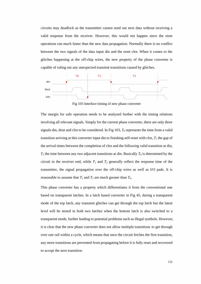
132
circuits may deadlock as the transmitter cannot send out next data without receiving a
valid response from the receiver. However, this would not happen since the reset
operations run much faster than the new data propagation. Normally there is no conflict
between the two signals of the data input din and the reset clrn. When it comes to the
glitches happening at the off-chip wires, the new property of the phase converter is
capable of ruling out any unexpected transient transitions caused by glitches.
T0 T1 T2
din
dout
clrn
Fig 103 Interface timing of new phase converter
The margin for safe operation needs to be analyzed further with the timing relations
involving all relevant signals. Simply for the current phase converter, there are only three
signals din, dout and clrn to be considered. In Fig 103, T0 represents the time from a valid
transition arriving at this converter input din to finishing self-reset with clrn, T1 the gap of
the arrival times between the completion of clrn and the following valid transition at din,
T2 the time between any two adjacent transitions at din. Basically T0 is determined by the
circuit in the receiver end, while T1 and T2 generally reflect the response time of the
transmitter, the signal propagation over the off-chip wires as well as I/O pads. It is
reasonable to assume that T1 and T2 are much greater than T0.
This phase converter has a property which differentiates it from the conventional one
based on transparent latches. In a latch based converter in Fig 45, during a transparent
mode of the top latch, any transient glitches can get through the top latch but the latest
level will be stored in both two latches when the bottom latch is also switched to a
transparent mode, further leading to potential problems such as illegal symbols. However,
it is clear that the new phase converter does not allow multiple transitions to get through
over one rail within a cycle, which means that once the circuit fetches the first transition,
any more transitions are prevented from propagating before it is fully reset and recovered
to accept the next transition.
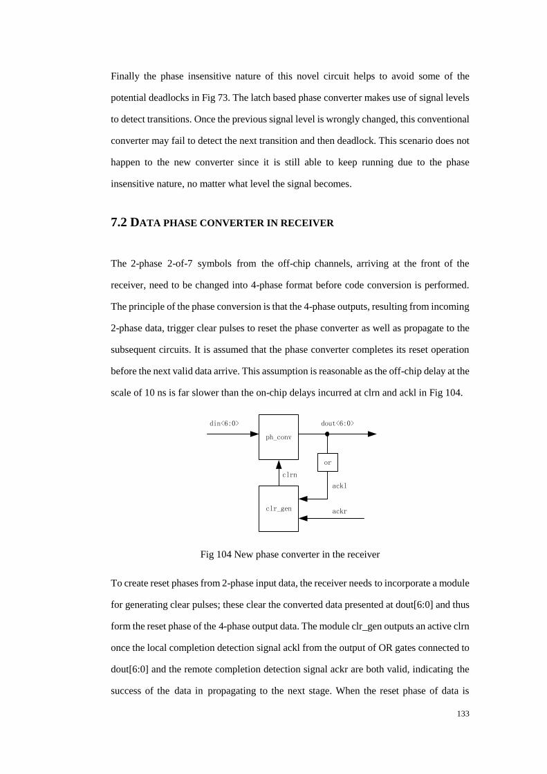
133
Finally the phase insensitive nature of this novel circuit helps to avoid some of the
potential deadlocks in Fig 73. The latch based phase converter makes use of signal levels
to detect transitions. Once the previous signal level is wrongly changed, this conventional
converter may fail to detect the next transition and then deadlock. This scenario does not
happen to the new converter since it is still able to keep running due to the phase
insensitive nature, no matter what level the signal becomes.
7.2 DATA PHASE CONVERTER IN RECEIVER
The 2-phase 2-of-7 symbols from the off-chip channels, arriving at the front of the
receiver, need to be changed into 4-phase format before code conversion is performed.
The principle of the phase conversion is that the 4-phase outputs, resulting from incoming
2-phase data, trigger clear pulses to reset the phase converter as well as propagate to the
subsequent circuits. It is assumed that the phase converter completes its reset operation
before the next valid data arrive. This assumption is reasonable as the off-chip delay at the
scale of 10 ns is far slower than the on-chip delays incurred at clrn and ackl in Fig 104.
ph_conv
clr_gen
or
din<6:0> dout<6:0>
clrn
ackr
ackl
Fig 104 New phase converter in the receiver
To create reset phases from 2-phase input data, the receiver needs to incorporate a module
for generating clear pulses; these clear the converted data presented at dout[6:0] and thus
form the reset phase of the 4-phase output data. The module clr_gen outputs an active clrn
once the local completion detection signal ackl from the output of OR gates connected to
dout[6:0] and the remote completion detection signal ackr are both valid, indicating the
success of the data in propagating to the next stage. When the reset phase of data is
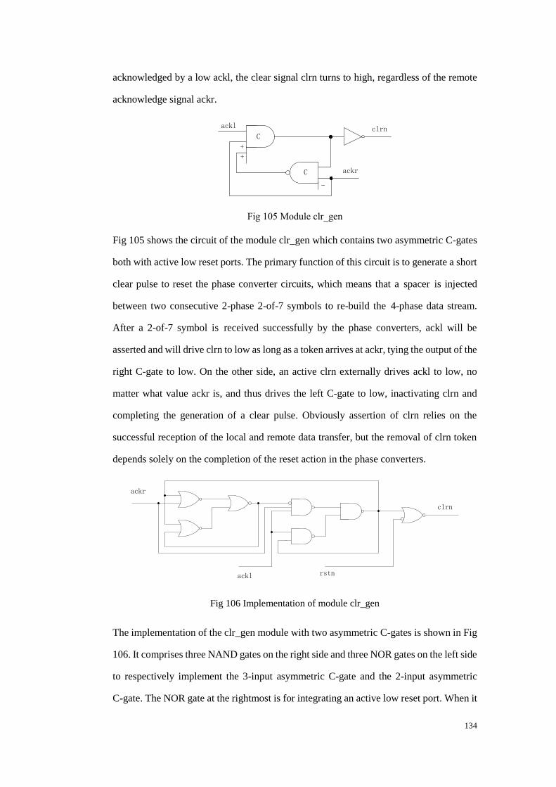
134
acknowledged by a low ackl, the clear signal clrn turns to high, regardless of the remote
acknowledge signal ackr.
+
+
ackl
-
C
C
clrn
ackr
Fig 105 Module clr_gen
Fig 105 shows the circuit of the module clr_gen which contains two asymmetric C-gates
both with active low reset ports. The primary function of this circuit is to generate a short
clear pulse to reset the phase converter circuits, which means that a spacer is injected
between two consecutive 2-phase 2-of-7 symbols to re-build the 4-phase data stream.
After a 2-of-7 symbol is received successfully by the phase converters, ackl will be
asserted and will drive clrn to low as long as a token arrives at ackr, tying the output of the
right C-gate to low. On the other side, an active clrn externally drives ackl to low, no
matter what value ackr is, and thus drives the left C-gate to low, inactivating clrn and
completing the generation of a clear pulse. Obviously assertion of clrn relies on the
successful reception of the local and remote data transfer, but the removal of clrn token
depends solely on the completion of the reset action in the phase converters.
ackr
ackl rstn
clrn
Fig 106 Implementation of module clr_gen
The implementation of the clr_gen module with two asymmetric C-gates is shown in Fig
106. It comprises three NAND gates on the right side and three NOR gates on the left side
to respectively implement the 3-input asymmetric C-gate and the 2-input asymmetric
C-gate. The NOR gate at the rightmost is for integrating an active low reset port. When it
135
comes to the clr_gen module robustness, its two inputs, ackl and ackr, need to be
considered. ackl comes from an OR gate tree connected to dout[6:] in Fig 104 while ackr
comes from the CD output of the subsequent pipeline register, which will be discussed in
Fig 117. The propagation time of ackr, about one C-gate and CD delays, is greater than
the 3 levels of standard gate delays incurred on ackl. Moreover, the path delay from ackr
to clrn inside the clr_gen module is also 2 levels of standard gate delay greater than the
path delay from ackl to clrn. Thus this module designed and laid-out carefully will be safe
enough to operate.
Besides the resistance to glitches discussed in the previous section, this data phase
converter in the receiver is also able to filter out most glitches. In Fig 104 a glitch can get
through ph_conv and then trigger ackl, but clrn is fired only after ackr is asserted from the
next pipeline register, where a valid ackr indicates a success in receiving a symbol. If a
small skew exists between the two transitions of an input 2-of-7 symbol, it is more likely
for ph_conv to produce a more than 2-of-7 illegal symbol, but the circuit does not
deadlock. If a large skew occurs between the two transitions, the whole off-chip interface
may deadlock due to a potential handshake failure somewhere in the circuits. This is
similar to the conventional phase converter in these scenarios.
7.3 ACKNOWLEDGE PHASE CONVERTER IN THE TRANSMITTER
In a transmitter, the acknowledge signal from the off-chip 2-phase channel needs to be
converted into 4-phase with the phase converter before joining on-chip logic operations.
The circuit in Fig 107 illustrates the integration of the module ack_ph_conv, which is
already described in Fig 101, with other neighbouring modules in a transmitter.
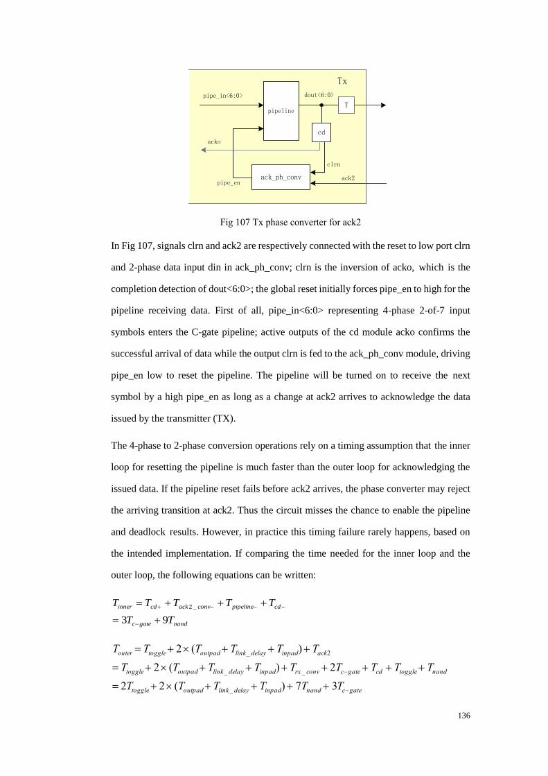
136
pipeline
cd
ack_ph_conv
pipe_in<6:0> dout<6:0>
ack2pipe_en
Tx
T
acko
clrn
Fig 107 Tx phase converter for ack2
In Fig 107, signals clrn and ack2 are respectively connected with the reset to low port clrn
and 2-phase data input din in ack_ph_conv; clrn is the inversion of acko, which is the
completion detection of dout<6:0>; the global reset initially forces pipe_en to high for the
pipeline receiving data. First of all, pipe_in<6:0> representing 4-phase 2-of-7 input
symbols enters the C-gate pipeline; active outputs of the cd module acko confirms the
successful arrival of data while the output clrn is fed to the ack_ph_conv module, driving
pipe_en low to reset the pipeline. The pipeline will be turned on to receive the next
symbol by a high pipe_en as long as a change at ack2 arrives to acknowledge the data
issued by the transmitter (TX).
The 4-phase to 2-phase conversion operations rely on a timing assumption that the inner
loop for resetting the pipeline is much faster than the outer loop for acknowledging the
issued data. If the pipeline reset fails before ack2 arrives, the phase converter may reject
the arriving transition at ack2. Thus the circuit misses the chance to enable the pipeline
and deadlock results. However, in practice this timing failure rarely happens, based on
the intended implementation. If comparing the time needed for the inner loop and the
outer loop, the following equations can be written:
nandgatec
cdpipelineconvackcdinner
TT
TTTTT
93
_2
Touter Ttoggle 2 (Toutpad Tlink_ delay Tinpad) Tack2
Ttoggle 2 (Toutpad Tlink_ delay Tinpad) Trx _ conv 2Tcgate Tcd Ttoggle Tnand
2Ttoggle 2 (Toutpad Tlink_ delay Tinpad) 7Tnand 3Tcgate
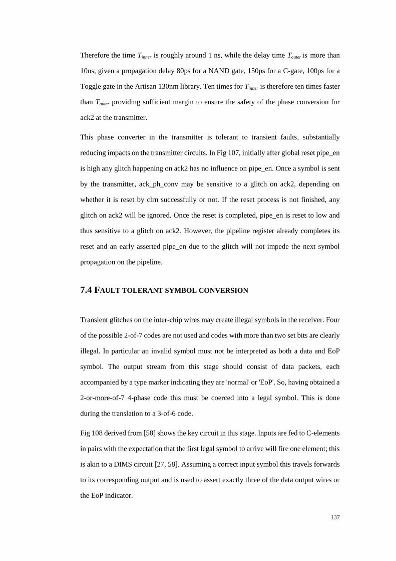
137
Therefore the time Tinner is roughly around 1 ns, while the delay time Touter is more than
10ns, given a propagation delay 80ps for a NAND gate, 150ps for a C-gate, 100ps for a
Toggle gate in the Artisan 130nm library. Ten times for Tinner is therefore ten times faster
than Touter providing sufficient margin to ensure the safety of the phase conversion for
ack2 at the transmitter.
This phase converter in the transmitter is tolerant to transient faults, substantially
reducing impacts on the transmitter circuits. In Fig 107, initially after global reset pipe_en
is high any glitch happening on ack2 has no influence on pipe_en. Once a symbol is sent
by the transmitter, ack_ph_conv may be sensitive to a glitch on ack2, depending on
whether it is reset by clrn successfully or not. If the reset process is not finished, any
glitch on ack2 will be ignored. Once the reset is completed, pipe_en is reset to low and
thus sensitive to a glitch on ack2. However, the pipeline register already completes its
reset and an early asserted pipe_en due to the glitch will not impede the next symbol
propagation on the pipeline.
7.4 FAULT TOLERANT SYMBOL CONVERSION
Transient glitches on the inter-chip wires may create illegal symbols in the receiver. Four
of the possible 2-of-7 codes are not used and codes with more than two set bits are clearly
illegal. In particular an invalid symbol must not be interpreted as both a data and EoP
symbol. The output stream from this stage should consist of data packets, each
accompanied by a type marker indicating they are 'normal' or 'EoP'. So, having obtained a
2-or-more-of-7 4-phase code this must be coerced into a legal symbol. This is done
during the translation to a 3-of-6 code.
Fig 108 derived from [58] shows the key circuit in this stage. Inputs are fed to C-elements
in pairs with the expectation that the first legal symbol to arrive will fire one element; this
is akin to a DIMS circuit [27, 58]. Assuming a correct input symbol this travels forwards
to its corresponding output and is used to assert exactly three of the data output wires or
the EoP indicator.
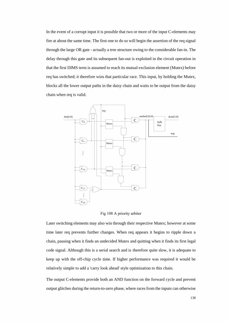
138
In the event of a corrupt input it is possible that two or more of the input C-elements may
fire at about the same time. The first one to do so will begin the assertion of the req signal
through the large OR gate - actually a tree structure owing to the considerable fan-in. The
delay through this gate and its subsequent fan-out is exploited in the circuit operation in
that the first DIMS term is assumed to reach its mutual exclusion element (Mutex) before
req has switched; it therefore wins that particular race. This input, by holding the Mutex,
blocks all the lower output paths in the daisy chain and waits to be output from the daisy
chain when req is valid.
C0
C1
Mutex
Mutex
C16Mutex
C17
din[6:0] onehot[16:0]
3of6
Enc
dout[5:0]
req
C20
eop
C
C
C
C
Fig 108 A priority arbiter
Later switching elements may also win through their respective Mutex; however at some
time later req prevents further changes. When req appears it begins to ripple down a
chain, pausing when it finds an undecided Mutex and quitting when it finds its first legal
code signal. Although this is a serial search and is therefore quite slow, it is adequate to
keep up with the off-chip cycle time. If higher performance was required it would be
relatively simple to add a 'carry look ahead' style optimisation to this chain.
The output C-elements provide both an AND function on the forward cycle and prevent
output glitches during the return-to-zero phase, where races from the inputs can otherwise

139
- in principle - expose a 'lower priority' request briefly if the inputs are zeroed with
significant skew.
7.5 FAULT TOLERANT SYMBOL DETECTION
Considering the incomplete 2-of-7 and 3-of-6 DI code used in the interface circuit, all
data are conveyed with a subset of each code and therefore none of the unused symbols
appears through the whole link. However, in the presence of glitches the unused symbols
may be presented in the circuits, especially in the receiver since the transient glitches can
be combined with the normal transitions to introduce illegal symbols.
For an illegal symbol, a completion detection module fails to generate a valid output
indicating a successful reception of a symbol, which means that no acknowledge token is
issued back from the completion detection module to reset the previous C-gate pipeline.
If we assume that the two transitions always arrive sooner or later, even though a transient
glitch is inserted before or after the first correct transition and they are interpreted as an
illegal symbol the circuit will wait for the next transition. In this case, the two transitions
plus the transient glitch finally trigger the output of the completion detection module.
Fig 109 shows the completion detection circuit which supports the complete 2-of-7 code.
Compared to the circuit supporting the incomplete 2-of-7 code, there are four C-gates at
the bottom of the figure added to cover detection of all other unused symbols. Therefore it
can be seen that the area overhead is still acceptable. Additionally, the initial completion
detection circuit is retained for incomplete 3-of-6 code, as the 3-of-6 symbols are
relatively clean and there are no unused symbols presented at the input of the detection
modules. However, the complete code detection may not be helpful to increase the
circuits‟ fault tolerance. If a glitch combined with a valid transition forms an illegal
symbol, the completion detector produces a premature acknowledge signal, which may
jeopardize the circuits. In this scenario, an incomplete code detector helps to remove the
propagation of illegal symbols over the circuits. But if the glitch forms a correct symbol

140
with that valid transition, the incomplete code detector behaves the same as a complete
code detector.
Fig 109 Completion detection of complete 2-of-7 code
7.6 FAULT TOLERANT PACKET TRANSFER - FLIT COUNTER
In the presence of glitches, missed EoP symbols or additional false symbols in a packet
can lead to framing errors. The communications NoC fabric may run out of buffer space if
an over-length packet arrives and occupies all available buffer space, causing deadlock
over the input links of the on-chip router. Packets in the SpiNNaker system have two
valid lengths: 10 flits and 18 flits. The receiver needs to check the length of any received
packets ensure an EoP is signalled at least every 18 flits and generate a framing error
signal to tag the packet in cases where the EoP symbol is missed or superfluous data are
received.
flit_cnt
{EoP,normal}
acko
{EoP,normal}
acki
ctrl_inctrl_out
Frame_err (dual rail)
Fig 110 Flit counter
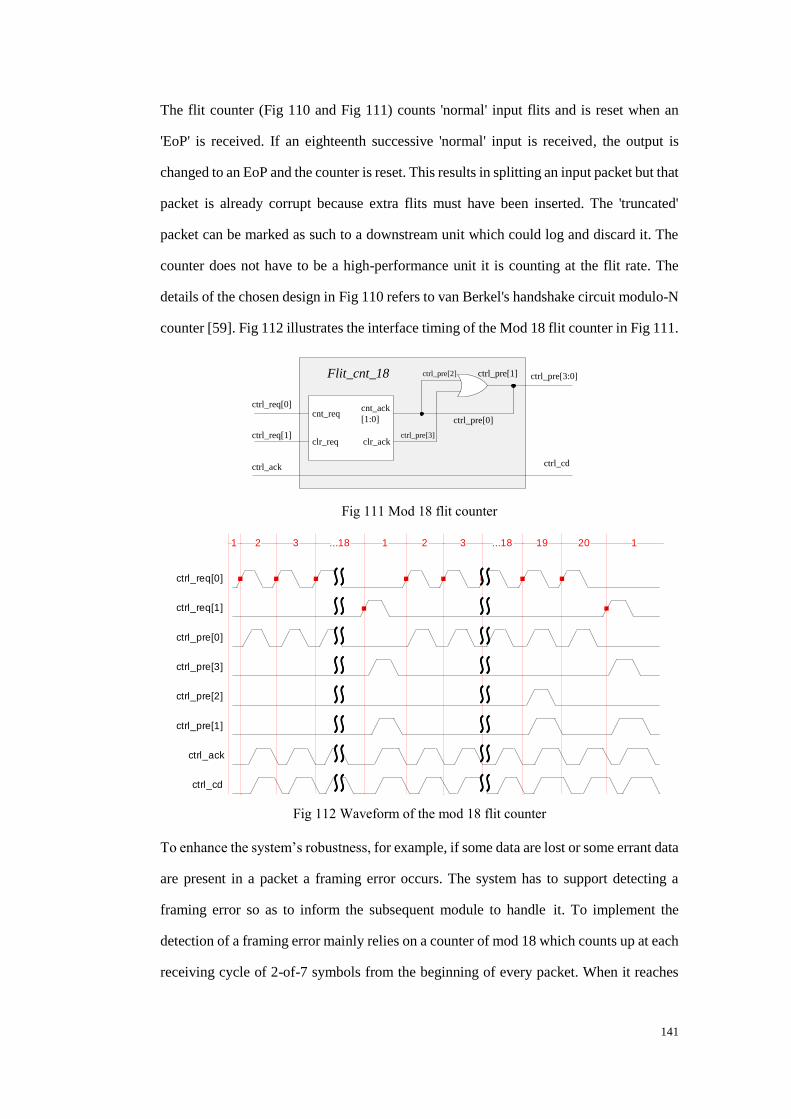
141
The flit counter (Fig 110 and Fig 111) counts 'normal' input flits and is reset when an
'EoP' is received. If an eighteenth successive 'normal' input is received, the output is
changed to an EoP and the counter is reset. This results in splitting an input packet but that
packet is already corrupt because extra flits must have been inserted. The 'truncated'
packet can be marked as such to a downstream unit which could log and discard it. The
counter does not have to be a high-performance unit it is counting at the flit rate. The
details of the chosen design in Fig 110 refers to van Berkel's handshake circuit modulo-N
counter [59]. Fig 112 illustrates the interface timing of the Mod 18 flit counter in Fig 111.
cnt_req
clr_req
cnt_ack
[1:0]
clr_ack
ctrl_req[0]
ctrl_req[1]
ctrl_pre[0]
ctrl_pre[2] ctrl_pre[1]
ctrl_pre[3]
ctrl_ack ctrl_cd
ctrl_pre[3:0]Flit_cnt_18
Fig 111 Mod 18 flit counter
1 2 3 ...18 1 2 3 ...18 19 20 1
ctrl_req[0]
ctrl_req[1]
ctrl_pre[0]
ctrl_pre[3]
ctrl_pre[2]
ctrl_pre[1]
ctrl_ack
ctrl_cd
Fig 112 Waveform of the mod 18 flit counter
To enhance the system‟s robustness, for example, if some data are lost or some errant data
are present in a packet a framing error occurs. The system has to support detecting a
framing error so as to inform the subsequent module to handle it. To implement the
detection of a framing error mainly relies on a counter of mod 18 which counts up at each
receiving cycle of 2-of-7 symbols from the beginning of every packet. When it reaches
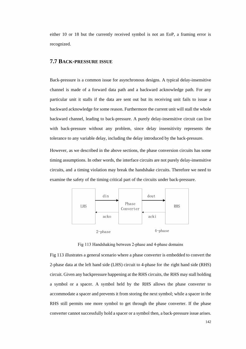
142
either 10 or 18 but the currently received symbol is not an EoP, a framing error is
recognized.
7.7 BACK-PRESSURE ISSUE
Back-pressure is a common issue for asynchronous designs. A typical delay-insensitive
channel is made of a forward data path and a backward acknowledge path. For any
particular unit it stalls if the data are sent out but its receiving unit fails to issue a
backward acknowledge for some reason. Furthermore the current unit will stall the whole
backward channel, leading to back-pressure. A purely delay-insensitive circuit can live
with back-pressure without any problem, since delay insensitivity represents the
tolerance to any variable delay, including the delay introduced by the back-pressure.
However, as we described in the above sections, the phase conversion circuits has some
timing assumptions. In other words, the interface circuits are not purely delay-insensitive
circuits, and a timing violation may break the handshake circuits. Therefore we need to
examine the safety of the timing critical part of the circuits under back-pressure.
LHSPhase
ConverterRHS
din dout
acko acki
2-phase 4-phase
Fig 113 Handshaking between 2-phase and 4-phase domains
Fig 113 illustrates a general scenario where a phase converter is embedded to convert the
2-phase data at the left hand side (LHS) circuit to 4-phase for the right hand side (RHS)
circuit. Given any backpressure happening at the RHS circuits, the RHS may stall holding
a symbol or a spacer. A symbol held by the RHS allows the phase converter to
accommodate a spacer and prevents it from storing the next symbol; while a spacer in the
RHS still permits one more symbol to get through the phase converter. If the phase
converter cannot successfully hold a spacer or a symbol then, a back-pressure issue arises.
143
A back-pressure tolerant circuit is expected to successfully accept the data after any large
time delay without data loss or deadlock. The conventional phase converter described
based on transparent latches is able to undergo the back-pressure in that the converter
detects signal level rather than transitions. However, the phase-insensitive converter we
proposed does not meet this requirement. As pointed out, it contains a self-reset circuit
which clears the received data through a self-timed pulse in Fig 104 and Fig 105. After
each symbol is received by the phase converter and forwarded to its output, an active acki
produces a clear pulse to reset the converter. The next symbol gets through the converter
and propagates to the RHS circuit as long as acki returns back to zero. In the presence of
back-pressure acki remains high till the back-pressure disappears; the next symbol
continues to arrive at the output port dout despite the fact that the RHS circuit cannot
accommodate any more symbols. In Fig 105, when the RHS holding a symbol in the
presence of back-pressure, the phase converter fails to reset itself and is therefore unable
to create spacers due to ackr remaining high. Consequently the RHS circuit will merge
this input symbol with its already stored symbol together. Furthermore, the missed
spacers cause deadlock in the receiver as it merges the new symbol with the previous one
without issuing back a valid acko signal. Note that if the RHS is holding a spacer when
back pressure takes place then it will not deadlock.
To eliminate the impact of back-pressure on the packet loss, the phase converter and the
RHS circuit need be enhanced to make them capable of separating and holding the input
symbols, rather than merging symbols if back-pressure is present.
pipeline1
cd
din dout
acki
ack2
Phase conv
pipeline0
T
Fig 114 Back-pressure tolerant pipelines
An effective way is to enhance the pipeline circuit after the phase converter. The circuit is
enhanced by adding one more standard C-gate pipeline in Fig 114, where the left C-gate
144
pipeline is dedicated to accommodate spacers in the presence of back-pressure. The
adjacent circuit at the output of the enhanced pipeline is saturated due to back-pressure
and the input signal acki is tied low so that the pipeline1 is only allowed to keep the
symbol which remains at the port dout and fails to propagate to the next pipeline stage.
The output of the cd module for the signal dout produces the acknowledge signal acko
and also clamps pipeline0 to pass a spacer. Even though the phase converter completes
the reset phase, the spacer generated by the self-timed clear pulse proceeds to pipeline0.
From now on all the circuits following the phase converter are frozen until the
back-pressure disappears. Assuming the next symbol represented by transitions arrives at
the phase converter and a symbol then appears at the port din, the pipeline0 and the
subsequent circuits, however, remain still. Thus the enhanced C-gate pipeline integrated
into the receiver effectively resolves the back-pressure issue.
The cost of the enhanced pipeline is trivial in that the pipeline0, the phase converter and
the output acknowledge to the transmitter share a signal acko. If acko goes high, it
enables the pipeline0 to take spacers, it resets the phase converter and it permits the
transmitter to issue next symbol. The first two operations take place simultaneously. In
addition, acko going low means that the pipeline0 is able to take a valid symbol.
Considering that the critical path is from the off-chip links, the arrival of a valid symbol
lags behind the reset completion of the pipelines when there is no back-pressure.
Therefore the added pipeline0 does not degrade the throughput generally.
7.8 FAULT TOLERANT RECEIVER ARCHITECTURE
As described in chapter 4, the initial receiver must acquire and hold two consecutive
symbols and the sequence of the pipeline outputs then determines the control output
symbol, either NORMAL or EoP. However the initial receiver architecture has a
potential problem from the fault tolerance perspective. Fig 53 shows that the sequence
detection is implemented in the domain of 2-of-7 symbols which may contain errant
symbols due to transient glitches. For instance, if an EoP and a data symbol are both
detected this receiver architecture is incapable of dealing with this error scenario.
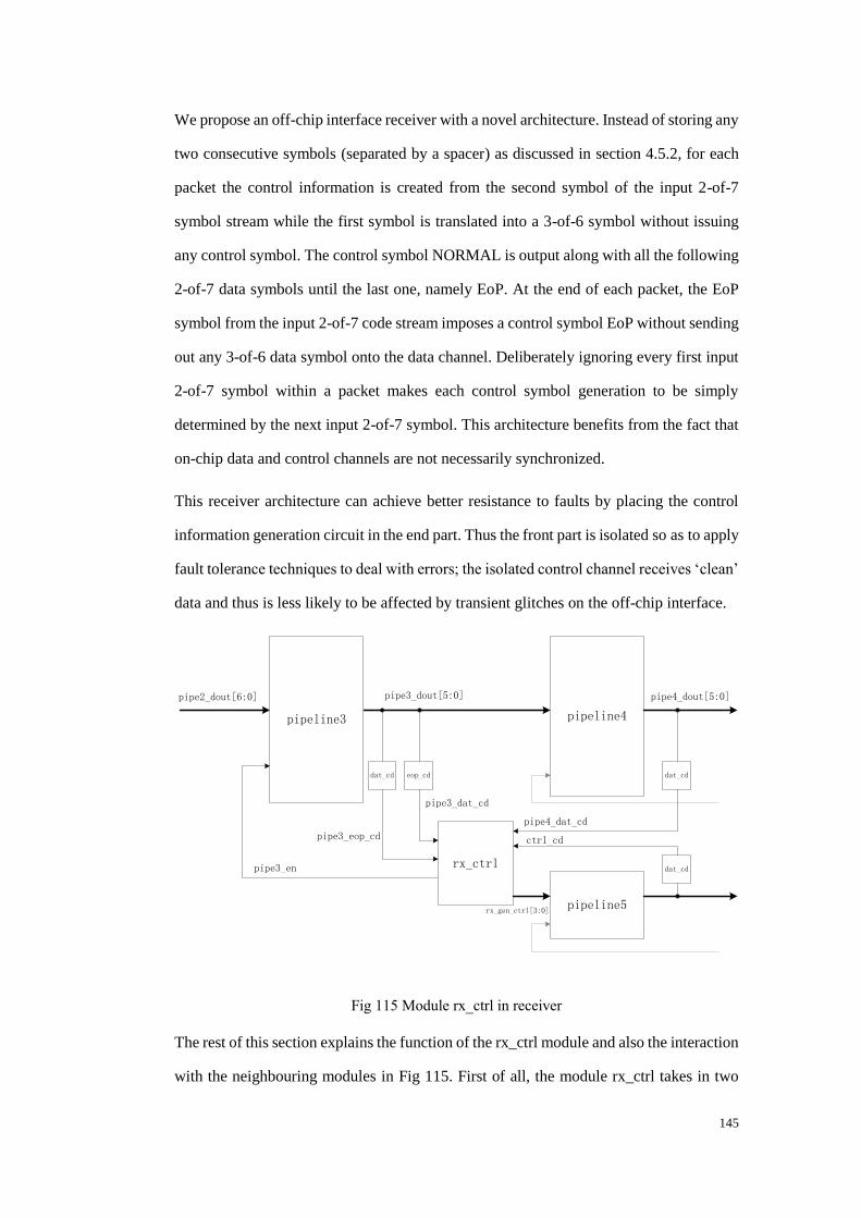
145
We propose an off-chip interface receiver with a novel architecture. Instead of storing any
two consecutive symbols (separated by a spacer) as discussed in section 4.5.2, for each
packet the control information is created from the second symbol of the input 2-of-7
symbol stream while the first symbol is translated into a 3-of-6 symbol without issuing
any control symbol. The control symbol NORMAL is output along with all the following
2-of-7 data symbols until the last one, namely EoP. At the end of each packet, the EoP
symbol from the input 2-of-7 code stream imposes a control symbol EoP without sending
out any 3-of-6 data symbol onto the data channel. Deliberately ignoring every first input
2-of-7 symbol within a packet makes each control symbol generation to be simply
determined by the next input 2-of-7 symbol. This architecture benefits from the fact that
on-chip data and control channels are not necessarily synchronized.
This receiver architecture can achieve better resistance to faults by placing the control
information generation circuit in the end part. Thus the front part is isolated so as to apply
fault tolerance techniques to deal with errors; the isolated control channel receives „clean‟
data and thus is less likely to be affected by transient glitches on the off-chip interface.
pipeline4
rx_ctrl
dat_cd eop_cd dat_cd
pipeline3
ctrl_cd
pipeline5
dat_cd
pipe3_dout[5:0] pipe4_dout[5:0]
pipe3_dat_cd
pipe3_eop_cd
pipe4_dat_cd
pipe3_en
rx_gen_ctrl[3:0]
pipe2_dout[6:0]
Fig 115 Module rx_ctrl in receiver
The rest of this section explains the function of the rx_ctrl module and also the interaction
with the neighbouring modules in Fig 115. First of all, the module rx_ctrl takes in two
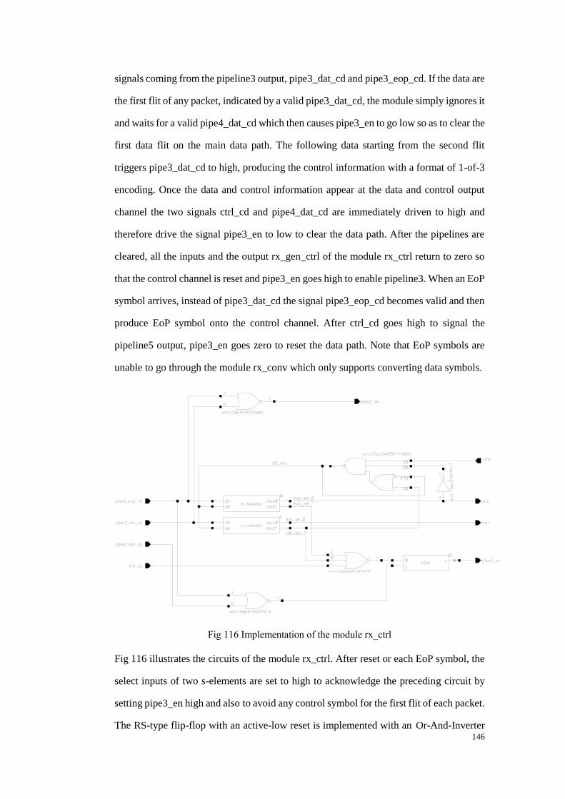
146
signals coming from the pipeline3 output, pipe3_dat_cd and pipe3_eop_cd. If the data are
the first flit of any packet, indicated by a valid pipe3_dat_cd, the module simply ignores it
and waits for a valid pipe4_dat_cd which then causes pipe3_en to go low so as to clear the
first data flit on the main data path. The following data starting from the second flit
triggers pipe3_dat_cd to high, producing the control information with a format of 1-of-3
encoding. Once the data and control information appear at the data and control output
channel the two signals ctrl_cd and pipe4_dat_cd are immediately driven to high and
therefore drive the signal pipe3_en to low to clear the data path. After the pipelines are
cleared, all the inputs and the output rx_gen_ctrl of the module rx_ctrl return to zero so
that the control channel is reset and pipe3_en goes high to enable pipeline3. When an EoP
symbol arrives, instead of pipe3_dat_cd the signal pipe3_eop_cd becomes valid and then
produce EoP symbol onto the control channel. After ctrl_cd goes high to signal the
pipeline5 output, pipe3_en goes zero to reset the data path. Note that EoP symbols are
unable to go through the module rx_conv which only supports converting data symbols.
Fig 116 Implementation of the module rx_ctrl
Fig 116 illustrates the circuits of the module rx_ctrl. After reset or each EoP symbol, the
select inputs of two s-elements are set to high to acknowledge the preceding circuit by
setting pipe3_en high and also to avoid any control symbol for the first flit of each packet.
The RS-type flip-flop with an active-low reset is implemented with an Or-And-Inverter
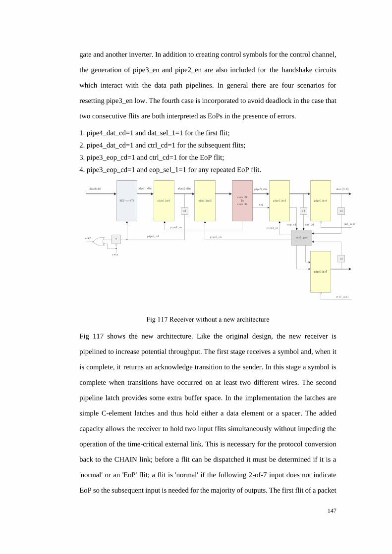
147
gate and another inverter. In addition to creating control symbols for the control channel,
the generation of pipe3_en and pipe2_en are also included for the handshake circuits
which interact with the data path pipelines. In general there are four scenarios for
resetting pipe3_en low. The fourth case is incorporated to avoid deadlock in the case that
two consecutive flits are both interpreted as EoPs in the presence of errors.
1. pipe4_dat_cd=1 and dat_sel_1=1 for the first flit;
2. pipe4_dat_cd=1 and ctrl_cd=1 for the subsequent flits;
3. pipe3_eop_cd=1 and ctrl_cd=1 for the EoP flit;
4. pipe3_eop_cd=1 and eop_sel_1=1 for any repeated EoP flit.
pipeline3 pipeline4pipeline1
cd
pipeline5
ctrl_gen
cd
cd
cd
eop_cd dat_cd
NRZ-to-RTZ
T
rstn
din[6:0] dout[5:0]
ctrl_acki
dat_ackipipe1_en
pipe2_en
pipe3_en
pipeline2code 27
Tocode 36
pipe1_cdack2
pipe1_din pipe2_din pipe3_din
eop
Fig 117 Receiver without a new architecture
Fig 117 shows the new architecture. Like the original design, the new receiver is
pipelined to increase potential throughput. The first stage receives a symbol and, when it
is complete, it returns an acknowledge transition to the sender. In this stage a symbol is
complete when transitions have occurred on at least two different wires. The second
pipeline latch provides some extra buffer space. In the implementation the latches are
simple C-element latches and thus hold either a data element or a spacer. The added
capacity allows the receiver to hold two input flits simultaneously without impeding the
operation of the time-critical external link. This is necessary for the protocol conversion
back to the CHAIN link; before a flit can be dispatched it must be determined if it is a
'normal' or an 'EoP' flit; a flit is 'normal' if the following 2-of-7 input does not indicate
EoP so the subsequent input is needed for the majority of outputs. The first flit of a packet

148
is sent after the second is received and so forth with the last data being freed by the input
EoP symbol.
The third pipeline stage converts the 2-of-7 input into a legal 3-of-6 output. For simplicity
the 2-of-7 code is first translated into a 'one hot' code by examining all possible legal pairs
of inputs. The single, chosen 1-of-17 code can then be ORed into its appropriate 3-of-6
data symbol or signal EoP. The last stage of the pipeline has already been described. This
retains a data symbol until pushed out by the subsequent symbol which is used to
determine its type. Because an EoP accompanies data on the output side the receiver does
not stall between packets.
7.9 INDEPENDENT RESET SCHEME
A resetting scheme is also implemented in circuits which essentially recover the interface
circuits when the asynchronous interconnect communication deadlocks due to either
transient glitches or other reasons above the circuit level, such as routing problems. In
particular, all the designs discussed above do not guarantee that the interface circuit is
able to eliminate all potential problems.
An efficient resetting scheme is desired to minimize the cost and the data loss.
Individually resetting the transmitter or the receiver on a dead inter-chip link is much
faster and easier to implement than a global reset. In fact, concurrently resetting both the
receiver and the transmitter on a link is difficult to coordinate from both sides and is also
costly in terms of response time and packet loss. The independent reset scheme allows
either the receiver or the transmitter to reset the dead inter-chip link and restart the
communication.
To support the individual reset, the circuits of the receiver and the transmitter both need to
be finalized. Once either end of an inter-chip link is reset, false symbols or false
acknowledge tokens may be created. The other live end has to tolerate these unexpected
input tokens.
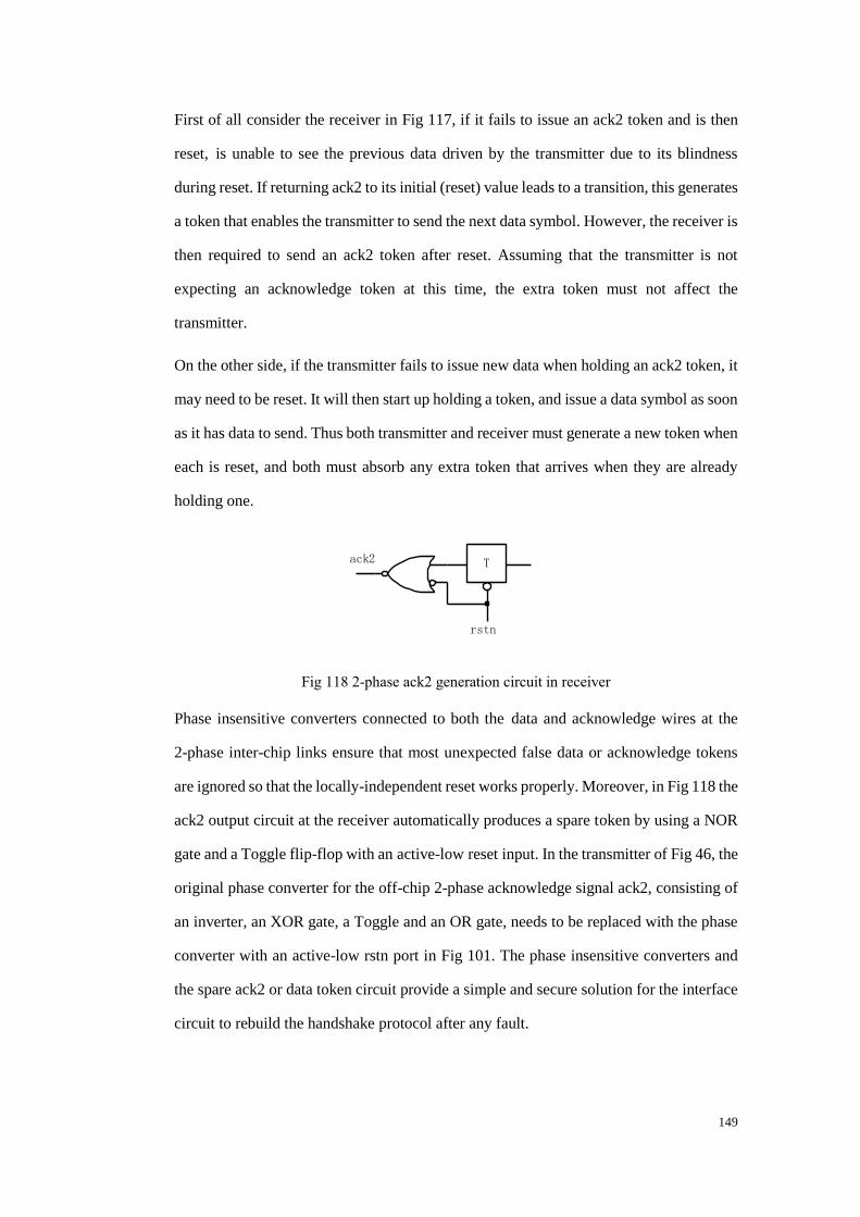
149
First of all consider the receiver in Fig 117, if it fails to issue an ack2 token and is then
reset, is unable to see the previous data driven by the transmitter due to its blindness
during reset. If returning ack2 to its initial (reset) value leads to a transition, this generates
a token that enables the transmitter to send the next data symbol. However, the receiver is
then required to send an ack2 token after reset. Assuming that the transmitter is not
expecting an acknowledge token at this time, the extra token must not affect the
transmitter.
On the other side, if the transmitter fails to issue new data when holding an ack2 token, it
may need to be reset. It will then start up holding a token, and issue a data symbol as soon
as it has data to send. Thus both transmitter and receiver must generate a new token when
each is reset, and both must absorb any extra token that arrives when they are already
holding one.
T
rstn
ack2
Fig 118 2-phase ack2 generation circuit in receiver
Phase insensitive converters connected to both the data and acknowledge wires at the
2-phase inter-chip links ensure that most unexpected false data or acknowledge tokens
are ignored so that the locally-independent reset works properly. Moreover, in Fig 118 the
ack2 output circuit at the receiver automatically produces a spare token by using a NOR
gate and a Toggle flip-flop with an active-low reset input. In the transmitter of Fig 46, the
original phase converter for the off-chip 2-phase acknowledge signal ack2, consisting of
an inverter, an XOR gate, a Toggle and an OR gate, needs to be replaced with the phase
converter with an active-low rstn port in Fig 101. The phase insensitive converters and
the spare ack2 or data token circuit provide a simple and secure solution for the interface
circuit to rebuild the handshake protocol after any fault.
150
7.10 SUMMARY
In this chapter, a new receiver was designed using a „divide-and-conquer‟ strategy. First
of all, a novel phase converter was invented. This can detect transitions on the off-chip
2-phase channel in a different way from the phase converter based on two transparent
latches. During the self-timed recovery phase all transitions - mostly glitches – are
ignored. Any positive or negative transitions occurring at other times will not be missed.
This new phase converter can avoid the deadlock scenario discussed in section 5.4.3. Its
phase-insensitive property can avoid another kind of deadlock resulting from a phase
error in an off-chip wire caused by a glitch.
Secondly, superfluous symbols caused by glitches were cleaned up in the new receiver.
Illegal symbols cannot propagate through the code converter. A priority arbiter allows
only one 3-of-6 symbol to be generated even when multiple 2-of-7 symbols
simultaneously appear at the input of the code converter in the presence of glitches.
Thus the impact of transient glitches on the 3-of-6 channel in the receiver is further
minimized.
Additionally, a counter is used in the receiver to detect a framing error caused by extra
symbols in a packet, thereby avoiding buffer overflows. Finally, the receiver
architecture is re-considered so as to reduce the influence of glitches on the generation
of control information. All control symbols are extracted from a relatively clean 3-of-6
and EoP stream at the priority arbiter output. The next chapter will illustrate the
effectiveness of these fault tolerant approaches by extensive simulation.
151
Chapter 8 FAULT SIMULATION RESULTS
This chapter describe the establishment of the simulation platform used to investigate
error efforts in the presence of transient glitches and also verify the effectiveness of the
proposed fault tolerance circuits against glitches. In addition, the design and fault
simulation methodology is also presented. Finally the fault simulation results are given to
compare the area and performance overhead and resistance against transient glitches of
the baseline design and two fault tolerant designs. The extensive simulations are finally
extended for generalized glitches and links with different duration and speed
respectively.
8.1 FAULT SIMULATION PLATFORM
A universal simulation platform to investigate interface circuit fault tolerance is proposed.
There are several benefits to applying this universal simulation platform; it works as a
functional verification platform that provides random packet generation for testing the
normal functions of the interface circuits. On the other hand, one distinct feature of the
platform is random glitch injection. This feature enables fault simulation with
configurable duration and occurrence frequency and random selection of victim wires.
Finally the simulation platform incorporates an automatic verification of test results to
support an extensive simulation with a large number of test packets.
An issue in performing fault simulation is the sparse distribution of glitches in the
simulation as transient glitches are not frequent. For example, a single glitch may occur
every few hours. Thus we cannot simulate the transient faults at a realistic occurrence
frequency due to the extremely long simulation time. Instead we accelerate the fault
simulation process by increasing the fault occurrence frequency up to one glitch per two
packets. Additionally, a large number of test packets are taken to give extensive
simulation, which exposes the target interface circuits to more glitches. The extensive
simulation reduces the possibility of missing potential errors.
152
TX RXData
TransmittingData
Receiving
Monitor
I/F
Fig 119 Simulation platform diagram
The platform primarily consists of a data transmitting module, a data receiving module
and a monitor module, as shown in Fig 119. The data transmitting module is responsible
for producing 3-of-6 symbols and 1-of-3 symbols and injecting them into the data and
control channels of the transmitter unit under test; while the data receiving module
converts the received symbols on the data and control channels into binary data and
frames them into packets. The monitor unit is in charge of random test packet generation,
random glitch generation, test packet verification and link error detection and recovery.
All these modules were implemented only for fault simulation rather than integrated into
the real circuits for in-circuit testing and monitoring.
8.1.1 MONITOR BLOCK
The monitor module in Fig 120 primarily consists of three sub-modules, a packet
generator, a glitch generator and a test result analyzer. The packet generator module
supports specifying the packet format and configures parameters regarding the packets,
for example, the number of test packets and the interval between transmitting two packets.
The second module, the Glitch generator, specifies a few parameters for defining a glitch,
such as glitch duration and frequency; a random scheme picks a victim data or
acknowledge wire at any time on the off-chip channel. The final module called the
Analyzer checks test results through the CRC field in every received packet; it detects if
any error happened in the packets and calculates the required statistics for the result
analysis, such as the packet loss rate.
153
AnalyzerGlitchGen
PacketGen
Monitor
Fig 120 Monitor block
The packet generation sub-module produces random data to simulate SpiNNaker packets
as there is no need to generate real neural spike packets in order to investigate fault effects
at the hardware level in this research. Data randomization, constraints and complex data
structures such as classes, as enhanced features in System-Verilog, allow random packets
with a similar packet structure to that of SpiNNaker packets, such as source/destination
address, payload and checksum, to be easily produced. In the SpiNNaker project, there
are only two types of packet in terms of their length, 5 byte and 9 byte packets. A
constraint on packet length randomly produces these two types of packets. Moreover, the
total number of test packets is also a user-defined parameter; normally a large number, for
example 1 million, is set to perform extensive simulation.
The glitch generator is one of the key modules as it supports the fault simulation with
random glitch injection. A glitch is defined with a class in SystemVerilog, in which all the
properties of a glitch are explicitly specified, including the configurable glitch frequency
and the glitch duration. The glitch class also defines a random variable representing a
victim wire hit by a glitch; this variable randomly picks an off-chip wire out of seven data
wires and one acknowledge wire at an off-chip channel, into which a transient glitch is
injected. Moreover, the other parameter, the glitch duration, is also randomized within a
customized range to simulate a particular group of random transient glitches.
The final major function of the monitor, implemented in the module analyzer, is to check
the packets received from the on-chip receiver circuit. Without injecting glitches, this
verification function can test the normal functionality of the off-chip interface circuits.
154
Particularly due to lack of a fast and efficient timing test methodology like static timing
analysis in synchronous circuits, performing dynamic simulation with test patterns is
essential to detect any design faults. Data verification is usually realized by comparing
the received packets with a reference data library, containing an exact copy of generated
packets from the data transmitting block.
However, some difficulties will arise when we perform fault simulation for the target
interface circuits. The difficulties in the fault simulation result from the diversity of the
errors caused by glitches on asynchronous interconnect. For example, a superfluous EoP
symbol appearing in the received data sequence splits the sent packet into two packets,
while a missed EoP error merges two consecutive packets into one. Both cases cause
more difficulties in the monitor block to properly synchronize the reference data library
and the received packets. By contrast, checking the CRC field in a packet is a more
efficient and less costly verification method than comparison of received packets with
reference packets in the fault simulation. In the packet generator described above, a 16-bit
CRC value is calculated and filled in the CRC field of each packet; the monitor module
calculates CRC values to verify all received packets.
In a noisy environment, however, this function is intended to calculate the number of
erroneous packets, the packet loss rate and other statistics by checking the correctness of
packet data. In addition, this module monitors the off-chip channel and detects whether it
has been idle for an exceptionally long period much greater than the specified interval
time between two consecutive packets. This indicates that deadlock has been detected.
The interface circuits need to be reset to continue the fault simulation and so further
explore the possibility of suffering from another deadlock or other kinds of error effects.
8.1.2 DATA TRANSMITTING MODULE
In the data transmitting module in Fig 121, an output packet buffer, a 3-of-6 encoder and
a byte transmitting processor are implemented to issue test packets to an on-chip
transmitter under test.
155
Out Packet buffer
3-of-6 Enc
Byte TX
Fig 121 Data transmitting Block
The output buffer stores the test packets generated by the packet generation module and
data bytes are sent to the 3-of-6 encoder. The 3-of-6 encoder sub-module receives the
random packet data from the data generation sub-module and converts them into a set of
3-of-6 symbols. For example, a 5-byte packet is turned into a sequence of 60-bit data,
which contains exactly ten 3-of-6 symbols since one 3-of-6 symbol carries 4-bit binary
data. The byte processor transmits 3-of-6 symbols of a randomly generated packet to the
data channel and also produces corresponding 1-of-3 symbols for the control channel,
particularly sending EoP symbols for last data symbols and Normal control symbols for
the other data symbols in each packet.
8.1.3 DATA RECEIVING BLOCK
A data receiving module is connected to a receiver under test, which sits at the other end
of an off-chip channel. It contains a byte receiving processor, a 3-of-6 decoder and a
packet storage module, see Fig 122.
In Packet Buffer
3-of-6 Dec
Byte RX
Fig 122 Data receiving block
The data receiving block is the part interfacing to the receiver circuit. Similar to the data
transmitting block but in a reverse order, the 3-of-6 symbols issued by the receiver circuit
first go through the Byte RX block where the handshaking protocol is designed to fetch
data and feed back acknowledge signals at the data channel in parallel with the control
channel. The data sampled by the Byte Rx block then need to be converted into binary
values in the 3-of-6 decoder. Finally a set of the binary values is recorded as one packet in
the input packet buffer. All test packet data are available to be verified and analysed in the
monitor module described above.
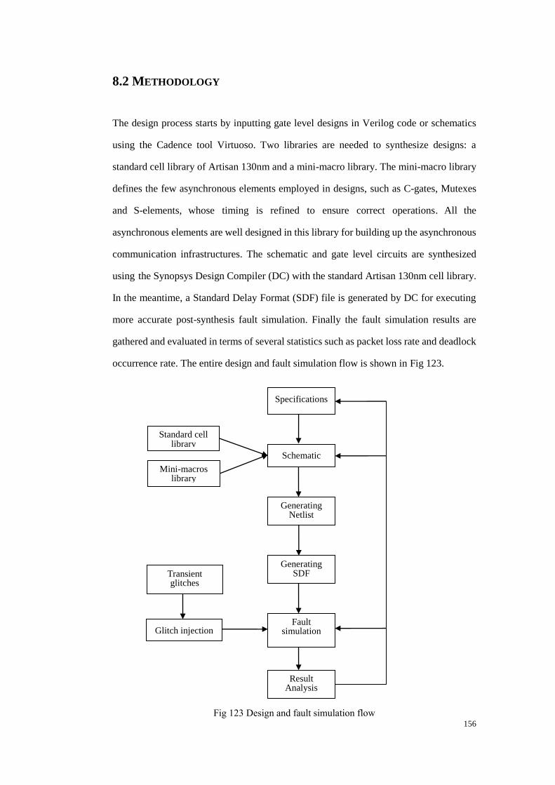
156
8.2 METHODOLOGY
The design process starts by inputting gate level designs in Verilog code or schematics
using the Cadence tool Virtuoso. Two libraries are needed to synthesize designs: a
standard cell library of Artisan 130nm and a mini-macro library. The mini-macro library
defines the few asynchronous elements employed in designs, such as C-gates, Mutexes
and S-elements, whose timing is refined to ensure correct operations. All the
asynchronous elements are well designed in this library for building up the asynchronous
communication infrastructures. The schematic and gate level circuits are synthesized
using the Synopsys Design Compiler (DC) with the standard Artisan 130nm cell library.
In the meantime, a Standard Delay Format (SDF) file is generated by DC for executing
more accurate post-synthesis fault simulation. Finally the fault simulation results are
gathered and evaluated in terms of several statistics such as packet loss rate and deadlock
occurrence rate. The entire design and fault simulation flow is shown in Fig 123.
Fig 123 Design and fault simulation flow
Schematic
Mini-macros library
Standard cell library
Generating SDF
Fault simulation
Transient glitches
Result Analysis
Glitch injection
Generating Netlist
Specifications
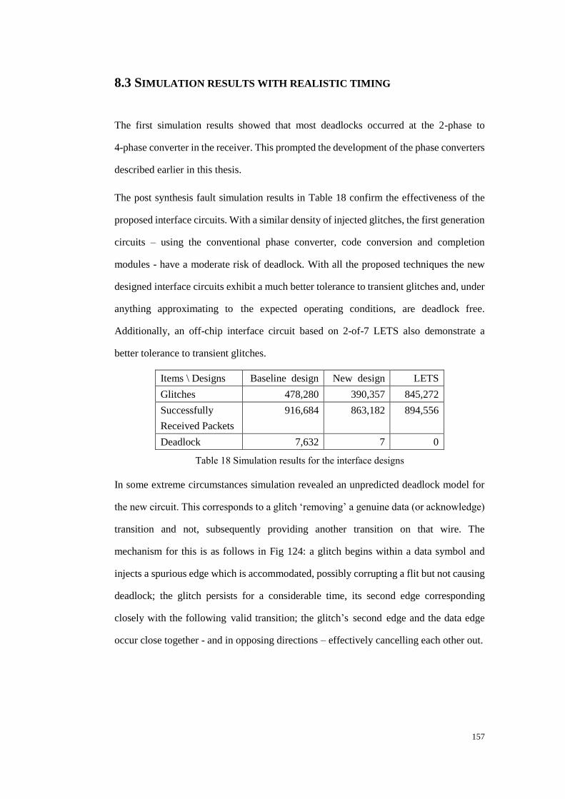
157
8.3 SIMULATION RESULTS WITH REALISTIC TIMING
The first simulation results showed that most deadlocks occurred at the 2-phase to
4-phase converter in the receiver. This prompted the development of the phase converters
described earlier in this thesis.
The post synthesis fault simulation results in Table 18 confirm the effectiveness of the
proposed interface circuits. With a similar density of injected glitches, the first generation
circuits – using the conventional phase converter, code conversion and completion
modules - have a moderate risk of deadlock. With all the proposed techniques the new
designed interface circuits exhibit a much better tolerance to transient glitches and, under
anything approximating to the expected operating conditions, are deadlock free.
Additionally, an off-chip interface circuit based on 2-of-7 LETS also demonstrate a
better tolerance to transient glitches.
Items \ Designs Baseline design New design LETS
Glitches 478,280 390,357 845,272
Successfully
Received Packets
916,684 863,182 894,556
Deadlock 7,632 7 0
Table 18 Simulation results for the interface designs
In some extreme circumstances simulation revealed an unpredicted deadlock model for
the new circuit. This corresponds to a glitch „removing‟ a genuine data (or acknowledge)
transition and not, subsequently providing another transition on that wire. The
mechanism for this is as follows in Fig 124: a glitch begins within a data symbol and
injects a spurious edge which is accommodated, possibly corrupting a flit but not causing
deadlock; the glitch persists for a considerable time, its second edge corresponding
closely with the following valid transition; the glitch‟s second edge and the data edge
occur close together - and in opposing directions – effectively cancelling each other out.
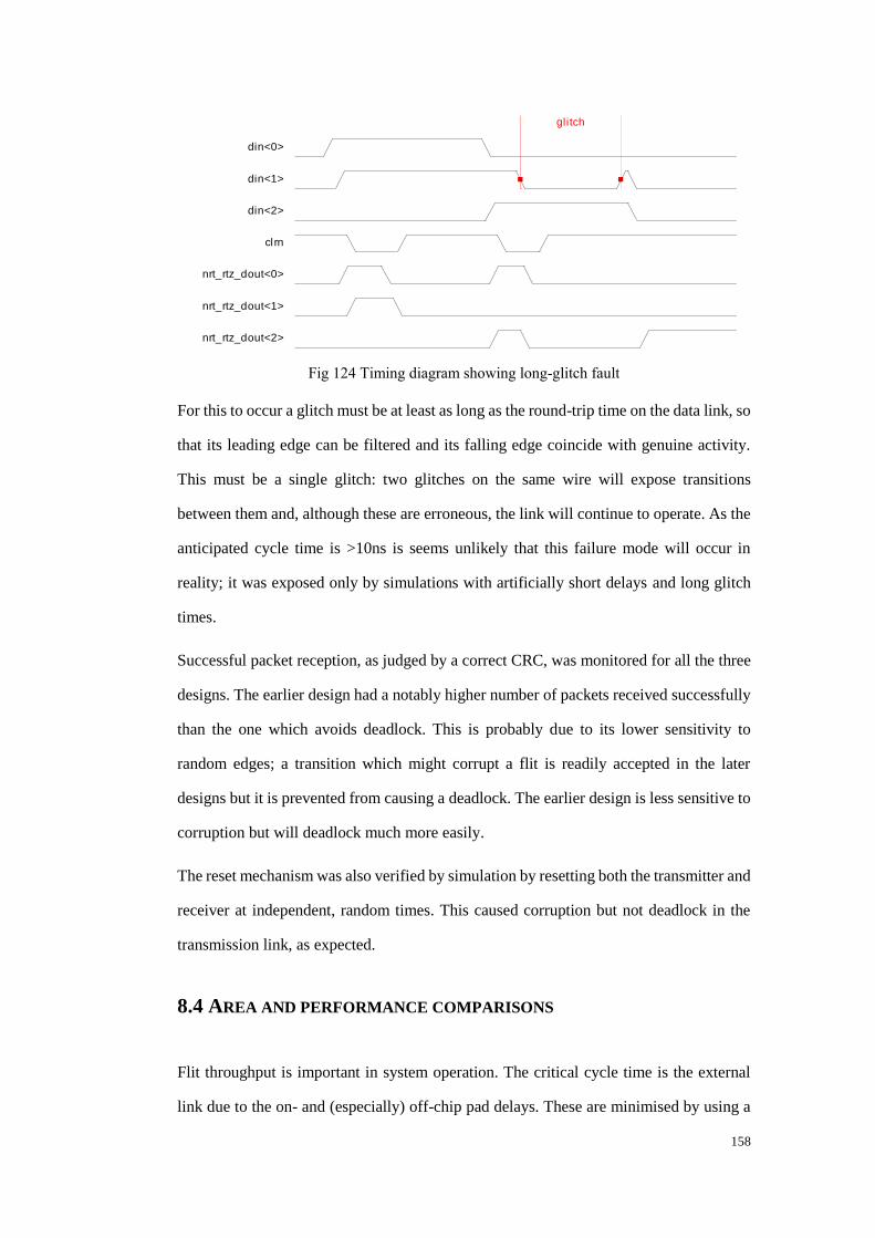
158
glitch
><0din
><1din
><2din
clrn
><0nrt_rtz_dout
><1nrt_rtz_dout
><2nrt_rtz_dout
Fig 124 Timing diagram showing long-glitch fault
For this to occur a glitch must be at least as long as the round-trip time on the data link, so
that its leading edge can be filtered and its falling edge coincide with genuine activity.
This must be a single glitch: two glitches on the same wire will expose transitions
between them and, although these are erroneous, the link will continue to operate. As the
anticipated cycle time is >10ns is seems unlikely that this failure mode will occur in
reality; it was exposed only by simulations with artificially short delays and long glitch
times.
Successful packet reception, as judged by a correct CRC, was monitored for all the three
designs. The earlier design had a notably higher number of packets received successfully
than the one which avoids deadlock. This is probably due to its lower sensitivity to
random edges; a transition which might corrupt a flit is readily accepted in the later
designs but it is prevented from causing a deadlock. The earlier design is less sensitive to
corruption but will deadlock much more easily.
The reset mechanism was also verified by simulation by resetting both the transmitter and
receiver at independent, random times. This caused corruption but not deadlock in the
transmission link, as expected.
8.4 AREA AND PERFORMANCE COMPARISONS
Flit throughput is important in system operation. The critical cycle time is the external
link due to the on- and (especially) off-chip pad delays. These are minimised by using a
159
2-phase protocol but the circuit efficiency can also influence this noticeably. The new
circuit cycles about 20% faster than its predecessor (see Table 19), some of which,
however is attributable to 'conventional' circuit improvements. Additionally, the 2-of-7
LETS based off-chip interface exhibits a high area overhead; its area is double that of the
former two designs. As a result, the performance is much lower due to the bigger circuits
though it could be further optimized to improve the performance, especially the
complexity of the 2-of-7 LETS encoder in the transmitter. Considering the high area
overhead and poor performance, the 2-of-7 LETS based design, it is not implemented in
SpiNNaker; while the implementation using hybrid fault tolerant techniques is
eventually chosen for fabrication.
Designs AREA(um2)
Performance(ns)
Total TX RX
Baseline 7010.1 6.4 1.1 5.3
New design 8555.7 5.0 1.5 3.5
LETS 16094.4 21.6 17.5 4.1
Table 19 Comparisons of area and performance
Although the size of the interfaces is a small part of a SpiNNaker chip it is still desirable
to keep overheads down as much as possible. Sample layouts have been constructed in a
130nm UMC process which indicates that the highly glitch-resistant interface is about 4%
larger than its predecessor. This is not a high price to pay for the considerable increase in
reliability.
8.5 SIMULATION RESULTS WITH GENERALIZED GLITCHES AND LINKS
In addition to the extensive fault simulation performed with realistic timing, the analysis
was extended to explore the designs under generalized glitch conditions and
asynchronous link delays. Glitch durations are classified into three groups, short glitches,
medium glitches and long glitches, which have duration less than 1 ns, 1-2 ns and 2-10ns
respectively; the link speed is set as slow, typical and fast, defined as 10ns, 5ns and 1ns.
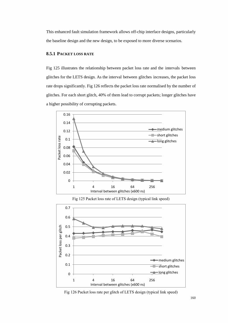
160
This enhanced fault simulation framework allows off-chip interface designs, particularly
the baseline design and the new design, to be exposed to more diverse scenarios.
8.5.1 PACKET LOSS RATE
Fig 125 illustrates the relationship between packet loss rate and the intervals between
glitches for the LETS design. As the interval between glitches increases, the packet loss
rate drops significantly. Fig 126 reflects the packet loss rate normalised by the number of
glitches. For each short glitch, 40% of them lead to corrupt packets; longer glitches have
a higher possibility of corrupting packets.
Fig 125 Packet loss rate of LETS design (typical link speed)
Fig 126 Packet loss rate per glitch of LETS design (typical link speed)
0
0.02
0.04
0.06
0.08
0.1
0.12
0.14
0.16
1 4 16 64 256
Pac
ket
loss
rat
e
Interval between glitches (x600 ns)
medium glitches
short glitches
long glitches
0
0.1
0.2
0.3
0.4
0.5
0.6
0.7
1 4 16 64 256
Pac
ket
loss
per
glit
ch
Interval between glitches (x600 ns)
medium glitches
short glitches
long glitches
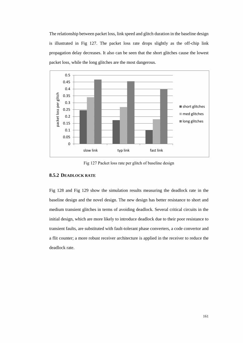
161
The relationship between packet loss, link speed and glitch duration in the baseline design
is illustrated in Fig 127. The packet loss rate drops slightly as the off-chip link
propagation delay decreases. It also can be seen that the short glitches cause the lowest
packet loss, while the long glitches are the most dangerous.
Fig 127 Packet loss rate per glitch of baseline design
8.5.2 DEADLOCK RATE
Fig 128 and Fig 129 show the simulation results measuring the deadlock rate in the
baseline design and the novel design. The new design has better resistance to short and
medium transient glitches in terms of avoiding deadlock. Several critical circuits in the
initial design, which are more likely to introduce deadlock due to their poor resistance to
transient faults, are substituted with fault-tolerant phase converters, a code convertor and
a flit counter; a more robust receiver architecture is applied in the receiver to reduce the
deadlock rate.
0
0.05
0.1
0.15
0.2
0.25
0.3
0.35
0.4
0.45
0.5
slow link typ link fast link
pac
ket
loss
per
glit
ch
short glitches
med glitches
long glitches
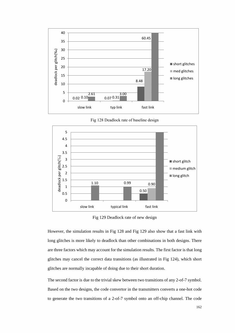
162
Fig 128 Deadlock rate of baseline design
Fig 129 Deadlock rate of new design
However, the simulation results in Fig 128 and Fig 129 also show that a fast link with
long glitches is more likely to deadlock than other combinations in both designs. There
are three factors which may account for the simulation results. The first factor is that long
glitches may cancel the correct data transitions (as illustrated in Fig 124), which short
glitches are normally incapable of doing due to their short duration.
The second factor is due to the trivial skew between two transitions of any 2-of-7 symbol.
Based on the two designs, the code convertor in the transmitters converts a one-hot code
to generate the two transitions of a 2-of-7 symbol onto an off-chip channel. The code
0.02 0.07
8.48
0.10 0.31
17.20
2.61 3.00
60.45
0
5
10
15
20
25
30
35
40
slow link typ link fast link
dea
dlo
ck p
er g
litch
(‰)
short glitches
med glitches
long glitches
0.50
0.901.10 0.99
0
0.5
1
1.5
2
2.5
3
3.5
4
4.5
5
slow link typical link fast link
dea
dlo
ck p
er g
litch
(‰)
short glitch
medium glitch
long glitch
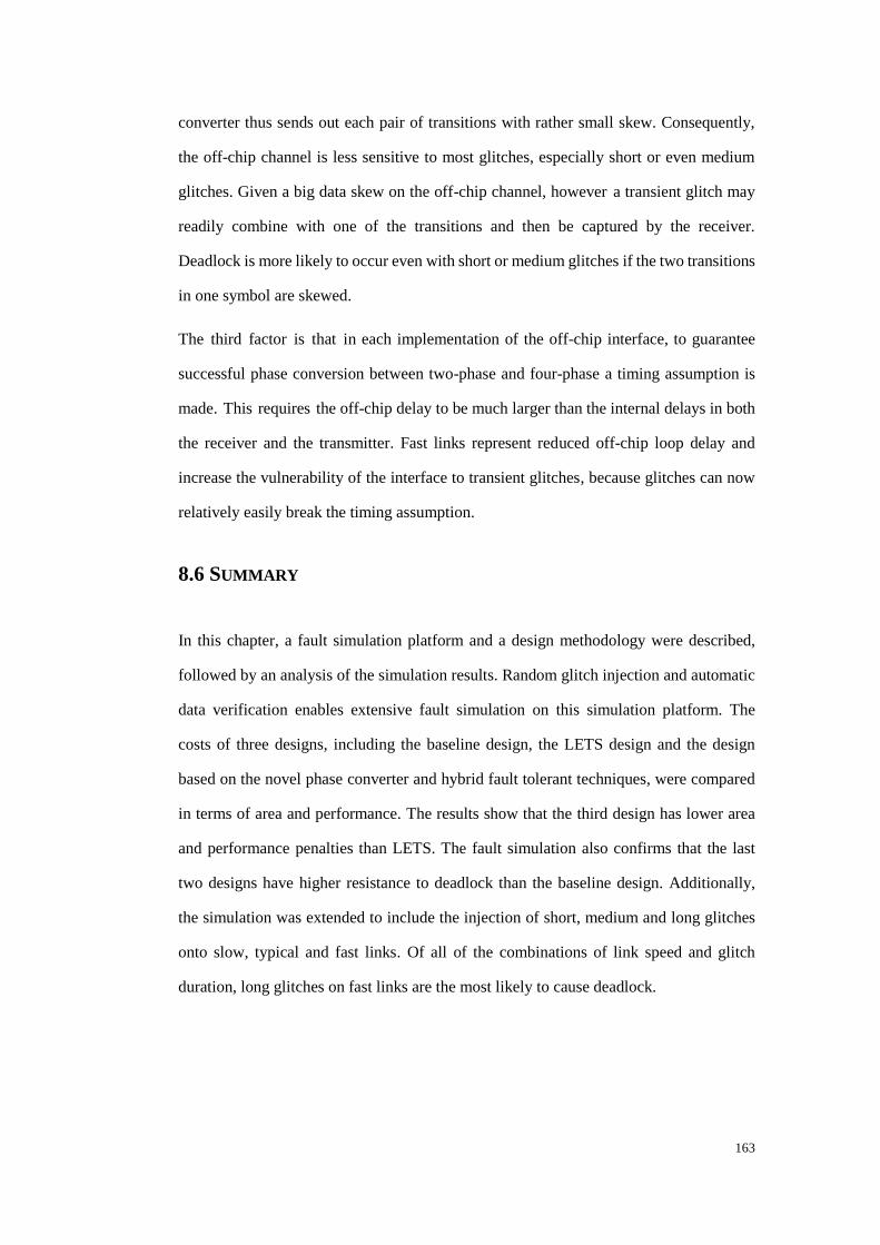
163
converter thus sends out each pair of transitions with rather small skew. Consequently,
the off-chip channel is less sensitive to most glitches, especially short or even medium
glitches. Given a big data skew on the off-chip channel, however a transient glitch may
readily combine with one of the transitions and then be captured by the receiver.
Deadlock is more likely to occur even with short or medium glitches if the two transitions
in one symbol are skewed.
The third factor is that in each implementation of the off-chip interface, to guarantee
successful phase conversion between two-phase and four-phase a timing assumption is
made. This requires the off-chip delay to be much larger than the internal delays in both
the receiver and the transmitter. Fast links represent reduced off-chip loop delay and
increase the vulnerability of the interface to transient glitches, because glitches can now
relatively easily break the timing assumption.
8.6 SUMMARY
In this chapter, a fault simulation platform and a design methodology were described,
followed by an analysis of the simulation results. Random glitch injection and automatic
data verification enables extensive fault simulation on this simulation platform. The
costs of three designs, including the baseline design, the LETS design and the design
based on the novel phase converter and hybrid fault tolerant techniques, were compared
in terms of area and performance. The results show that the third design has lower area
and performance penalties than LETS. The fault simulation also confirms that the last
two designs have higher resistance to deadlock than the baseline design. Additionally,
the simulation was extended to include the injection of short, medium and long glitches
onto slow, typical and fast links. Of all of the combinations of link speed and glitch
duration, long glitches on fast links are the most likely to cause deadlock.
164
Chapter 9 CONCLUSIONS
This thesis described some fault tolerant circuits intended to reduce the consequences of
transient glitches on the asynchronous inter-chip interfaces in SpiNNaker. In particular
the intent is to reduce the potential for deadlock; providing the link continues to run other
error correction schemes may be used to verify data integrity.
By analyzing the reasons for deadlock and comparing different 2-phase to 4-phase
conversion circuits, fault tolerant implementations of the inter-chip interfaces were
devised. There are three major fault-trapping stages. The greatest benefit was conveyed
by the phase-insensitive data and acknowledge converters; the second, a code conversion
stage with priority arbitration ensured that only legal symbols can reach the on-chip
network; finally a counter ensures that packet size is limited to within the size of later
buffers.
The extensive simulation results show that the implementation has a very high resistance
to deadlock and is able not only to keep running but also to convey packets successfully
for a high proportion of the time despite artificially rather intense noise. Although the
current circuit corrupts somewhat more packets than its predecessor this is due to glitches
being translated into symbols rather than deadlocks. Deadlock avoidance is regarded as
the most important consideration.
Under any circumstances reasonably close to the expected operating conditions it is
believed that the links are now deadlock free. The only deadlocks that have been found
were achieved by mixing artificially long 'glitches' with artificially short inter-chip delays.
The probability of glitch durations approximating the link's cycle time (or greater) and
then coincidentally cancelling a real signal is regarded as exceedingly small. In such an
event the link is still recoverable by a higher-level reset process.
The practical realisations of the circuits described here contain some delay assumptions.
For example, the off-chip acknowledgement is sent before the receiver's phase converter
has completed clearing. This races the inter-chip cycle time with an on-chip pulse
165
generation and, with the long, off-chip delays is very safe and speeds up the critical path
of the slowest cycle in the network. It would be a simple matter to alter this so as to delay
the acknowledge to the falling edge of the clear pulse if, for example, the 2-phase link had
much lower latency due to it being entirely on-chip. The 2-of-7 to 3-of-6 code converter
also exploits a delay model; a delay insensitive circuit using the same principle could be
produced but owing to significant fan-in and -out would be larger and slower.
In addition to these 'in-line' processes a local reset scheme allows either end of the link to
be reset independently at any time. Although this could corrupt a packet 'in flight' it -
together with the inbuilt error tolerance - allows the link to recover normal operation.
Thus, if some unpredicted fault mode causes a link deadlock a higher level process can
detect the lack of activity and reset it. In practice it is thought more likely that this single
chip reset may result from a watchdog following a software crash; either way it allows
system recovery when a single, faulting chip is reset.
In addition to the above fault-tolerant off-chip interface implementation, another
solution was explored in this thesis. The alternative circuits were built using a novel
2-of-7 LETS code. This new code scheme offers a different way to implement off-chip
2-phase interconnect, as an alternative to the conventional 2-phase 2-of-7 code. The two
transitions for each new symbol depend on the Hamming distance of the input binary
data from the 4-bit data value of the previous symbol. The encoding procedure is
complex, but the decoding is very simple. The decoded data come directly from the
encoded symbol or its inverse.
From the fault tolerance point of view, the major advantage of this 2-of-7 LETS code is
the independence between two adjacent symbols; in the baseline design the decoding of
a symbol depends on the previous symbol value. Thus the new receiver does not need to
store the previous symbol to decode the current symbol and thus is able to avoid
deadlocks in the conventional phase converter. Moreover, 4-bit single rail data can be
directly decoded from the off-chip 2-phase 2-of-7 symbols without converting to
4-phase 2-of-7 symbols as the baseline receiver does. The benefit is that the 4-bit single
rail data output can effectively reduce the possibility of illegal and multiple symbols
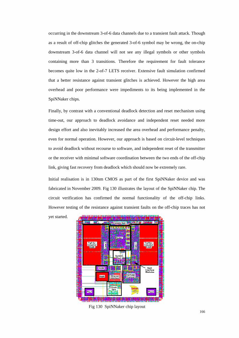
166
occurring in the downstream 3-of-6 data channels due to a transient fault attack. Though
as a result of off-chip glitches the generated 3-of-6 symbol may be wrong, the on-chip
downstream 3-of-6 data channel will not see any illegal symbols or other symbols
containing more than 3 transitions. Therefore the requirement for fault tolerance
becomes quite low in the 2-of-7 LETS receiver. Extensive fault simulation confirmed
that a better resistance against transient glitches is achieved. However the high area
overhead and poor performance were impediments to its being implemented in the
SpiNNaker chips.
Finally, by contrast with a conventional deadlock detection and reset mechanism using
time-out, our approach to deadlock avoidance and independent reset needed more
design effort and also inevitably increased the area overhead and performance penalty,
even for normal operation. However, our approach is based on circuit-level techniques
to avoid deadlock without recourse to software, and independent reset of the transmitter
or the receiver with minimal software coordination between the two ends of the off-chip
link, giving fast recovery from deadlock which should now be extremely rare.
Initial realisation is in 130nm CMOS as part of the first SpiNNaker device and was
fabricated in November 2009. Fig 130 illustrates the layout of the SpiNNaker chip. The
circuit verification has confirmed the normal functionality of the off-chip links.
However testing of the resistance against transient faults on the off-chip traces has not
yet started.
Fig 130 SpiNNaker chip layout
167
To conclude this thesis, a few fault tolerant techniques were devised to conquer
deadlock and other fault effects and verified for their effectiveness against
deadlock caused by transient faults.
Phase-insensitive data and acknowledge converters: they effectively avoid
deadlock in the conventional converters which transform signals between
2-phase and 4-phase protocols. Additionally, the insensitivity to signal level is
capable of preventing the circuits from stopping due to out-of-phase signals.
These novel converters are suitable for other applications requiring conversion
between 2-phase and 4-phase signals.
Priority based arbiter for symbol conversion: the generation of multiple
symbols in the presence of transient glitches can be avoided effectively with
this circuit so as to minimise their negative impact on the downstream circuits.
In this thesis, the arbiter implements the fault tolerant symbol conversion from
2-of-7 code into 3-of-6 code in the 4-phase domain. However, a Mutex based
arbiter can similarly be constructed to filter out multiple symbols.
Asynchronous framing error counter: this method is applicable to any
asynchronous NoC system to eliminate framing errors. In a case of extra data
in a packet, this module can prevent circuits from deadlocking due to buffer
congestion.
Improved architecture design of the receiver: the architecture of a system or
sub-system needs to be carefully examined in terms of resistance to all
potential error effects of transient faults. In each individual module, error
effects are isolated and prevented from propagating to subsequent circuits.
This strategy can increase the robustness of the system in the presence of
glitches while retaining a simple architecture.
LETS 2-of-7 code: this novel code scheme decouples the state dependency
between 2-phase symbols, implementing a new 2-phase interconnect different
from the conventional 2-phase interconnect. Along with LEDR and 1-of-4
168
LETS code, it provides another approach to the design of a fault tolerant
system based on a 2-phase and 4-phase hybrid interconnect.
Additionally, the independent resetting scheme, which allows either a dead
transmitter or a dead receiver to be reset without the participation of the other
end, considerably reduces the implementation complexity of a link resetting
scheme which would otherwise require a reset to be forced concurrently onto
both ends of the link. This strategy can be implemented in other kinds of
asynchronous interconnect, where a redundant ACK or data token can be
produced deliberately for successful reset in a similar way.
9.1 FUTURE WORK
This thesis has shown the feasibility of a few techniques, which can be implemented in
the off-chip interface of a SpiNNaker chip, to significantly increase the tolerance to
deadlock caused by transient glitches. In the future, it can be extended in the following
respects.
Firstly, the 2-of-7 LETS based off-chip interface circuits need further effort to optimize
their performance and reduce their area overhead. In particular, the transmitter needs to
be optimized due to the slow dual-rail logic used to build the Hamming distance
calculator. At the receiver end, the completion detection module directly connected to
the 2-phase off-chip input also requires a faster implementation so as to sample valid
2-phase off-chip 2-of-7 symbols as quickly as possible. This circuit delay is part of the
critical path of the receiver‟s cycle time. The optimization techniques considered here
are not only limited to the module level, but also include some particular circuit
techniques, such as buffer insertion.
Secondly, transient fault sources in the current simulation platform can be extended to
on-chip circuits, for example long wires between two pipeline registers, in addition to
their use for off-chip interconnect. Investigating the effects of transient faults on on-chip
interconnects will still emphasize deadlock issues. In particular, DI pipelines should be
examined for any misbehavior including deadlock in the presence of on-chip transient

169
faults. In recent 65nm and 45nm process technologies, these fault tolerant techniques
can be applied and examined.
Moreover, fault tolerance testing is needed to measure the efficiency of the tolerance
techniques to transient faults in real circuits. A few methods to inject faults into circuits
have been discussed elsewhere [60], including power noise, white light and laser fault
injection. However, faults need to be injected onto off-chip traces which are laid on a
printed circuit board. Thus aggressor traces are required to affect the victim traces
which are the off-chip wires. Basically, these aggressor traces which are redundant
traces with external inputs and dummy outputs can be designed deliberately on the PCB
for fault-tolerance testing purpose only. External signal generator outputs can be
connected to these traces. These means may produce controllable coupling crosstalk for
measuring the efficiency of the circuits under test.
Finally, formal verification may be a fast and efficient method which can examine the
immunity of an asynchronous interconnect to transient faults, particularly at the chip
layout stage. As seen in this thesis, performing extensive dynamic simulation is time
consuming and costly, and it is also difficult to analyze the simulation results and causes
of fault effects. A formal method to check handshake failures caused by potential
glitches would be very useful to establish a faster and more efficient tool for designing
fault-tolerant asynchronous DI interconnects.

170
REFERENCES
1. Borkar, S., Thousand core chips: a technology perspective. Proceedings of the
44th annual Design Automation Conference. ACM: San Diego, California, 2007.
2. May, T.C. and M.H. Woods, Alpha-particle-induced soft errors in dynamic
memories. IEEE Transactions on Electron Devices, 1979. 26(1): p. 2-9.
3. Baumann, R., Soft errors in advanced computer systems. Design & Test of
Computers, IEEE, 2005. 22(3): p. 258-266.
4. Chandra, V. and R. Aitken. Impact of voltage scaling on nanoscale SRAM
reliability. Design, Automation & Test in Europe Conference & Exhibition,
2009.
5. ITRS. 2007( Online Available: www.itrs.net).
6. Nassif, S.R., Modeling and forecasting of manufacturing variations (embedded
tutorial), Proceedings of the 2001 Asia and South Pacific Design Automation
Conference. ACM: Yokohama, Japan, 2001.
7. Normand, E., Single event upset at ground level. IEEE Transactions on Nuclear
Science, 1996. 43(6): p. 2742-2750.
8. LaFrieda, C. and R. Manohar, Fault Detection and Isolation Techniques for
Quasi Delay-Insensitive Circuits. Proceedings of the 2004 International
Conference on Dependable Systems and Networks. IEEE Computer Society,
2004. p. 41.
9. Peng, S. and R. Manohar, Efficient Failure Detection in Pipelined Asynchronous
Circuits. Proceedings of the 20th IEEE International Symposium on Defect and
Fault Tolerance in VLSI Systems. IEEE Computer Society, 2005. p. 484-493.
10. Jang, W. and A. Martin, SEU-Tolerant QDI Circuits. Proceedings of the 11th
IEEE International Symposium on Asynchronous Circuits and Systems. IEEE
Computer Society, 2005.
11. Kuang, W., C.M. Ibarra, and P. Zhao, Soft Error Hardening for Asynchronous
Circuits. Proceedings of the 22nd IEEE International Symposium on Defect and
Fault-Tolerance in VLSI Systems. IEEE Computer Society, 2007. p. 273-281.
12. Weidong, K., et al. Design Asynchronous Circuits for Soft Error Tolerance.
IEEE International Conference on Integrated Circuit Design and Technology,
2007.
13. Monnet, Y., M. Renaudin, and R. Leveugle, Asynchronous circuits transient
faults sensitivity evaluation. Proceedings of the 42nd annual Design Automation
Conference. ACM: Anaheim, California, USA, 2005.
14. Gardiner, K.T., A. Yakovlev, and A. Bystrov. A C-element Latch Scheme with
Increased Transient Fault Tolerance for Asynchronous Circuits. 13th IEEE
International On-Line Testing Symposium, 2007.
15. Bainbridge, W.J. and S.J. Salisbury, Glitch Sensitivity and Defense of Quasi
Delay-Insensitive Network-on-Chip Links. Proceedings of the 2009 15th IEEE

171
Symposium on Asynchronous Circuits and Systems. IEEE Computer Society ,
2009. p. 35-44.
16. Sutherland, I.E., Micropipelines, Communications of the ACM. 1989. 32(6)
p.720-738.
17. Singh, M. and S.M. Nowick. MOUSETRAP: ultra-high-speed
transition-signaling asynchronous pipelines. Proceedings of 2001 International
Conference on Computer Design, 2001.
18. Bainbridge, W.J. and S.B. Furber, Chain: A Delay-Insensitive Chip Area
Interconnect. IEEE Micro, 2002. 22(5): p. 16-23.
19. Furber, S.B., et al., A micropipelined ARM, Proceedings of the IFIP TC10/WG
10.5 International Conference on Very Large Scale Integration. North-Holland
Publishing Co,1994.
20. Furber, S.B., et al. AMULET2e: an asynchronous embedded controller. in
Advanced Research in Asynchronous Circuits and Systems. Third International
Symposium on Advanced Research in Asynchronous Circuits and Systems
(ASYNC '97), 1997.
21. Martin, A.J., et al., The Design of an Asynchronous MIPS R3000
Microprocessor. Proceedings of the 17th Conference on Advanced Research in
VLSI (ARVLSI '97). IEEE Computer Society,1997.
22. Martin, A.J., et al., The design of an asynchronous microprocessor. Proceedings
of the decennial Caltech conference on VLSI on Advanced research in VLSI.
MIT Press: Cambridge, Massachusetts, United States,1989.
23. Furber, S.B., et al., Power management in the Amulet microprocessors. Design &
Test of Computers, IEEE, 2001. 18(2): p. 42-52.
24. Berkel, K.V., Beware the isochronic fork. Integration, the VLSI Journal, 1992.
13(2): p. 103-128.
25. Bainbridge, W.J. and S.B. Furber. Delay insensitive system-on-chip interconnect
using 1-of-4 data encoding. in Asynchronous Circuits and Systems. Seventh
International Symposium on ASYNC, 2001.
26. Sparsø, J. and S.B. Furber, Principles of Asynchronous Circuit Design. Kluwer
Academic Publisher, 2001: p.67-69.
27. MULLER, D.E., Asynchronous Logics and Application to Information
Processing. Proc. Symp. Application of Switching Theory in Space Technology,
1963: p. 289-297.
28. Smith, S.C., et al., Optimization of NULL convention self-timed circuits.
Integration, the VLSI Journal, 2004. 37(3): p. 135-165.
29. Woods, J.V., et al., AMULET1: An Asynchronous ARM Microprocessor. IEEE
Transactions on Computers. 1997. 46(4): p. 385-398.
30. Chapiro, D.M., Globally-Asynchronous Locally-Synchronous Systems. 1984.
31. Guerrier, P. and A. Greiner, A generic architecture for on-chip packet-switched
interconnections. Proceedings of the conference on Design, Automation and test
in Europe in. ACM: Paris, France, 2000.
32. Dally, W.J. and B. Towles, Route Packets, Not Wires. The 38th ACM Design
Automation Conference. 2001.p. 684-689.

172
33. Benini, L. and G. De Micheli, Networks on chips: a new SoC paradigm.
Computer, 2002. 35(1): p. 70-78.
34. Andriahantenaina, A. and A. Greiner. Micro-network for SoC: implementation of
a 32-port SPIN network. Design, Automation and Test in Europe Conference and
Exhibition, 2003.
35. Goossens, K., J. Dielissen, and A. Radulescu, AEthereal network on chip:
concepts, architectures, and implementations. Design & Test of Computers,
IEEE, 2005. 22(5): p. 414-421.
36. Dall'Osso, M., et al. Xpipes: a latency insensitive parameterized network-on-chip
architecture for multiprocessor SoCs. 21st International Conference on
Computer Design, 2003.
37. Millberg, M., et al. The Nostrum backbone-a communication protocol stack for
Networks on Chip. 17th International Conference on VLSI Design, 2004.
38. ITRS. 2001 (Online Available: www.itrs.net).
39. Bjerregaard, T. and J. Sparso, Implementation of guaranteed services in the
MANGO clockless network-on-chip. IEE Proceedings - Computers and Digital
Techniques, 2006. 153(4): p. 217-229.
40. Miro-Panades, I., et al. Physical Implementation of the DSPIN Network-on-Chip
in the FAUST Architecture. Second ACM/IEEE International Symposium on
Networks-on-Chip, NoCs 2008.
41. Bainbridge, W.J., et al., Delay-Insensitive, Point-to-Point Interconnect Using
M-of-N Codes. Proceedings of the 9th International Symposium on
Asynchronous Circuits and Systems. IEEE Computer Society, 2003.
42. Plana, L.A., et al., A GALS Infrastructure for a Massively Parallel
Multiprocessor. Design & Test of Computers, IEEE, 2007. 24(5): p. 454-463.
43. Furber, S.B. and A.D. Brown, Biologically-Inspired Massively-Parallel
Architectures - computing beyond a million processors. Proc. 9th International
Conference on the Application of Concurrency to System Design, Augsburg,
Germany, 2009: p. 3-12.
44. ARM, AMBA Specifications. Online available,
(http://infocenter.arm.com/help/topic/com.arm.doc.set.amba/index.html#specs).
45. Shufan, Y., et al. An admission control system for QoS provision on a best-effort
GALS interconnect. 8th International Conference on Application of Concurrency
to System Design, 2008.
46. Plana, L.A., et al. An On-Chip and Inter-Chip Communications Network for the
SpiNNaker Massively-Parallel Neural Net Simulator. Second ACM/IEEE
International Symposium on Networks-on-Chip, 2008.
47. Wu, J. and S. Furber, A Multicast Routing Scheme for a Universal Spiking Neural
Network Architecture. The Computer Journal, 2009. 53(3): p.280-288.
48. Xin, J., S.B. Furber, and J.V. Woods. Efficient modelling of spiking neural
networks on a scalable chip multiprocessor. IEEE World Congress on
Computational Intelligence, IEEE International Joint Conference on Neural
Networks. 2008.
173
49. Izhikevich, E.M., Simple Model of Spiking Neurons. IEEE Transactions on
Neural Networks 2003. 14(6).
50. Rast, A., et al., The Deferred Event Model for Hardware-Oriented Spiking
Neural Networks. Advances in Neuro-Information Processing: 15th International
Conference, ICONIP 2008, Auckland, New Zealand, November 25-28, 2008,
Revised Selected Papers, Part II. 2009, Springer-Verlag. p. 1057-1064.
51. Cortadella, J., et al., Petrify: a tool for manipulating concurrent specifications
and synthesis of asynchronous controllers. IEICE Transactions on Information
and Systems, 1997. E80-D(3): p. 315--325.
52. Group, U.D.V.C., Petrify: a tool for synthesis of Petri Nets and asynchronous
circuits, Online Available:http://www.lsi.upc.edu/~jordicf/petrify/.
53. Rosenblum, L. Y and A. Yakovlev, Signal Graphs: From Self-Timed to Timed
Ones, International Workshop on Timed Petri Nets. IEEE Computer Society,
1985.
54. Monnet, Y., M. Renaudin, and R. Leveugle, Asynchronous Circuits Sensitivity to
Fault Injection. Proceedings of the 10th IEEE International On-Line Testing
Symposium. IEEE Computer Society, 2004.
55. Dean, M.E., T.E. Williams, and D.L. Dill, Efficient self-timing with
level-encoded 2-phase dual-rail (LEDR). Proceedings of the 1991 University of
California/Santa Cruz conference on Advanced research in VLSI. MIT Press,
1991.
56. Mitra, A., W.F. McLaughlin, and S.M. Nowick, Efficient Asynchronous Protocol
Converters for Two-Phase Delay-Insensitive Global Communication.
Proceedings of the 13th IEEE International Symposium on Asynchronous
Circuits and Systems. IEEE Computer Society, 2007.
57. McGee, P.B., et al. A Level-Encoded Transition Signaling Protocol for
High-Throughput Asynchronous Global Communication. 14th IEEE
International Symposium on Asynchronous Circuits and Systems, 2008.
58. Felicijan, T., W.J. Bainbridge, and S.B. Furber. An asynchronous low latency
arbiter for Quality of Service (QoS) applications. ICM Proceedings of the 15th
International Conference on Microelectronics, 2003.
59. Berkel, K.V., Handshake circuits: an asynchronous architecture for VLSI
programming. Cambridge University Press,1993.
60. Monnet, Y., M. Renaudin, and R. Leveugle, Designing resistant circuits against
malicious faults injection using asynchronous logic. IEEE Transactions on
Computers, 2006. 55(9).


![Theory of latency-insensitive design - Computer-Aided ...luca/research/lipTransactions.pdf · delay-insensitive circuits [19], [20]. A delay-insensitive circuit is designed to operate](https://img.pdfslide.net/doc/110x75/5e77b28d15933b649935c2f3/theory-of-latency-insensitive-design-computer-aided-lucaresearchliptransactionspdf.jpg)