Embed Size (px)
Citation preview

FC_EE_201608_FrontCover_FINAL_eb.indd CoverIFC_EE_201608_FrontCover_FINAL_eb.indd CoverI 7/12/2016 9:12:40 AM7/12/2016 9:12:40 AM

I
©2016 National Instruments. All rights reserved. LabVIEW, National Instruments, NI, ni.com, and NI TestStand are trademarks of National Instruments. Other product and company names listed are trademarks or trade names of their respective companies. 25143
NI PXI, LabVIEW, and TestStand
S M A R T D E V I C E S R E Q U I R E
AUTOMATED TEST SYSTEMS
SMARTERThe old approach to automated test isn’t
scaling, but you already knew that. Look at your
balance sheet. To test smart devices, you need
a smarter test system built on a platform of NI
PXI, LabVIEW, and TestStand. More than 35,000
companies deploy NI technology to lower their
cost of test—what are you waiting for?
Prepare for the future at ni.com/smarter-test
IFC-01_EE_201608_TOC_FINAL_eb.indd CoverIIIFC-01_EE_201608_TOC_FINAL_eb.indd CoverII 7/7/2016 2:28:41 PM7/7/2016 2:28:41 PM

evaluationengineering.comAugust 2016 1
August 2016, Vol. 55, No.8
EE-EVALUATION ENGINEERING (ISSN 0149-0370). Published monthly by NP Communications, 2477 Stickney Point Rd., Ste. 221-B, Sarasota, FL 34231. Subscription rates: $176 per year in the United States; $193.60 per year in Canada/Mexico; International subscriptions are $224.40 per year. Current single copies, (if available) are $15.40 each (U.S.); $19.80 (international). Back issues, if available, are $17.60 each (U.S.) and $22 (international). Payment must be made in U.S. funds on a branch of a U.S. bank within the continental United States and accompany request. Subscription inquiries: [email protected].
Title® registered U.S. Patent Offi ce. Copyright© 2016 by NP Communications LLC. All rights reserved. No part of this publication may be reproduced or transmitted in any form or by any means, electronic or mechanical, including photocopy, recording, or any information storage-and-retrieval system, without permission in writing from the publisher.
Offi ce of publication: Periodicals Postage Paid at Sarasota, FL 34276 and at additional mailing offi ces. Postmaster: Send address changes to EE-EVALUATION ENGINEERING, P.O. BOX 17517, SARASOTA FL 34276-0517
Written by Engineers…for Engineers evaluationengineering.com
@EE_Engineers
www.facebook.com/EvaluationEngineering
C O N T E N T S
C O M M U N I C AT I O N S T E S TSPECIAL REPORT
5G Test6 Algorithms, instruments rev up 5G
By Rick Nelson, Executive Editor
Industry Happenings27 IMS sees chips and instruments
targeting mmWave applicationsBy Rick Nelson, Executive Editor
I N S T R U M E N TAT I O NSPECIAL REPORT
Modular DMMs10 DMMs extended and refi ned
By Tom Lecklider, Senior Technical Editor
Additive Manufacturing16 Building parts one layer at a time
By Tom Lecklider, Senior Technical Editor
Sensors24 Accurate and integrated temperature
measurement By Tom Lecklider, Senior Technical Editor
Industry Happenings26 Sensors Expo topics span MEMS
to robots and dronesBy Rick Nelson, Executive Editor
Research Insights32 GaN shows promise for transportation,
communications applicationsBy Rick Nelson, Executive Editor
AT E
Design for Test14 Impacting accuracy of chipmaker’s
quality testsBy Peter Sarson, Gregor Schatzberger, and Andreas Wild,
ams AG
E M C
EMC Product Focus28 Keeping EMI in its place
By Tom Lecklider, Senior Technical Editor
S P E C I A L F E AT U R E
Salary Survey20 Taking the pulse of the industry
By Tom Lecklider, Senior Technical Editor
D E PA R T M E N T S2 Editorial
4 EE Industry Update
30 EE Product Picks
31 Index of Advertisers
IFC-01_EE_201608_TOC_FINAL_eb.indd 1IFC-01_EE_201608_TOC_FINAL_eb.indd 1 7/8/2016 12:14:16 PM7/8/2016 12:14:16 PM

August 2016evaluationengineering.com2
EDITORIAL
EDITORIALEXECUTIVE EDITOR Rick Nelsone-mail: [email protected]
MANAGING EDITOR Deborah Beebee-mail: [email protected]
SENIOR TECHNICAL EDITOR Tom Lecklidere-mail: [email protected]
PRODUCTIONPRINT/WEB COORDINATOR Emily Baatz
e-mail: [email protected]/WEB COORDINATOR Glenn Huston
e-mail: [email protected] CONTRACTS MANAGER Laura Moulton
e-mail: [email protected] TRAFFIC MANAGER Denise Mathews
e-mail: [email protected]
BUSINESSPRESIDENT Kristine Russell
e-mail: [email protected]
PUBLISHER Jim Russelle-mail: [email protected]
ASSOCIATE PUBLISHER Michael Hughese-mail: [email protected]
MARKETING DIRECTOR Joan Sutherland
ADVERTISINGWEST
Michael Hughes Phone: 805-529-6790e-mail: [email protected]
EASTBlake Holton or Michelle Holton
Phone: 407-971-6286 or 407-971-8558e-mail: bholton@cfl .rr.com
mmholton@cfl .rr.com
CIRCULATIONSUBSCRIPTIONS / BACK ISSUES
e-mail: [email protected] RENTALS Laura Moulton e-mail: [email protected] COORDINATOR Mary Haberstroh e-mail: [email protected] Deborah Beebe
e-mail: [email protected]
EE-EVALUATION ENGINEERING is available by free subscription to qualifi ed managers, supervisors
and engineers in the electronics and related industries.
FOUNDER A. VERNER NELSONe-mail: [email protected]
NP COMMUNICATIONS LLC2477 Stickney Point Rd., Suite 221BSarasota, Florida 34231Phone: 941-388-7050•Fax: 941-388-7490
Publishers of this magazine assume no responsibility for statements made by their advertisers in business competition, nor do they assume responsibility for statements/opinions, expressed or implied, in the columns of this magazine.
Printed in the U.S.A.
evaluationengineering.com
RICK NELSON
Executive Editor
Visit my blog: www.evaluationengineering.com/ricks-blog/
From an email chain among a group of technical editors, the following questions recently arose: Why does the idea of mounting electronics in a 19-inch rack
persist? Further, why was 19 inches chosen in the fi rst place?As I point out in a recent blog post, Practical-Home-Theater-Guide.com traces
the 19-inch rack back to George Westinghouse in 1890, who used 19-inch shelving to house railroad relay gear. The site notes that telephone companies eventually adopted the 19-inch width, and the EIA standardized the 19-inch structure in 1965 with its 310-D standard.
According to Wikipedia (under the entry “19-inch rack”), a revised EIA standard in 1992 gave us today’s 1.752-inch (44.5-mm) 1U height.
Responses to my blog post offer several opinions. Brainstorms writes, “Ulti-mately, all dimensions are arbitrary. That they correspond to a nice, round num-ber [or prime number in the case of the 19-inch rack] in some equally arbitrary measurement system is coincidental (whether intended or not). Of course, those round numbers fascinate human beings. But what’s really of importance is that the dimensions be standardized and that those standards be adhered to by various manufacturers.”
Steve Alonso comments of the 19-inch dimension: “It ranks up there with the 4-foot 8.5-inch rail spacing based on the standard Roman chariot/cart width conforming to the width of two horses side-by-side.” The myth-busting website Snopes.com questions whether the rail gauge actually descended from Roman times, calling the claim that it did “… partly true, but for trivial and unremarkable reasons.” In any event, Alonso is certainly correct when he concludes, “We are all victims of historical choices for better or worse.”
Sam Simione writes, “… the 19-inch rack-mounting size is manageable and works well from the viewpoint of a practical size we can build, handle, mount, and ship. Also, 19-inch rack enclosures are built such that they are relatively mechani-cally stable even at 40 and 45U heights.” William Ketel agrees that a 19-inch assem-bly would be easy for one person to grab with both hands, adding that the width might be a multiple of the widths of the relays Westinghouse wanted to mount as well as a submultiple of a standard width of sheet metal available at the time.
Simione adds that anyone believing the size is not optimum for modern elec-tronics should bring the issue to the attention of the EIA.
In fact, there seems to be no need for revision. As Wikipedia notes, “The 19-inch rack format has remained constant while the technology that is mounted within it has changed considerably, and the set of fi elds to which racks are applied has greatly expanded.”
That’s for sure. The latest example of the technology that fi ts within the for-mat comes from National Instruments, with the introduction last month of its new PXIe-5840 vector signal transceiver, which combines a 6.5-GHz RF vector signal generator, a 6.5-GHz vector signal analyzer, a user-programmable FPGA, and high-speed serial and parallel digital interfaces.
Charles Schroeder, vice president of product marketing for RF at NI, said in a recent interview that NI engineers worked hard to fi t the new VST’s functional-ity into a two-slot PXI Express module. (The original VST, introduced in 2012, re-quired three slots.) They succeeded, enabling eight VST modules to fi t it in a single 18-slot, 19-inch chassis, forming an 8x8 MIMO test setup.
As Simione put it, “Whatever the reason for the 19-inch dimension, history has proved it was a good choice and is here to stay!”
Westinghouse’s 19-inch rack accommodates 8x8 MIMO test
02-03_EE_201608_Editorial_FINAL_eb.indd 202-03_EE_201608_Editorial_FINAL_eb.indd 2 7/7/2016 11:12:15 AM7/7/2016 11:12:15 AM

Visit www.rsleads.com/608ee-004
02-03_EE_201608_Editorial_FINAL_eb.indd 302-03_EE_201608_Editorial_FINAL_eb.indd 3 7/7/2016 11:12:42 AM7/7/2016 11:12:42 AM

August 2016evaluationengineering.com4
ChipMOS selects Xcerra test cell for high-volume MEMS testAfter evaluating several alternatives, ChipMOS has selected Xcerra’s total test cell solution as its preferred test platform for high-volume production of MEMS devices at its Shanghai facility. ChipMOS is a provider of semiconductor assembly and test services with factories in Hsin-chu and Southern Taiwan Science Parks in Taiwan and Shanghai. ChipMOS now is prepared to support further MEMS
fabless and IDM customers’ mobility, automotive, and IoT volume production requirements for MEMS calibration and test in Shanghai.
The Xcerra MEMS test cell incorpo-rates the cost-effi cient LTX-Credence Diamondx tester and the high-through-put Multitest InMEMS/InCarrier solu-tion. ChipMOS chose the Xcerra test cell solution because it combines Dia-mondx’s high parallel test capability with Multi test’s advanced package han-dling and MEMS stimulus options. The fully integrated solution delivers a pre-validated test cell directly to ChipMOS’s manufacturing fl oor, minimizing the time to high-volume production. The ini-tial cells are equipped to switch between high multisite testing of 3DOF magne-tometer devices on a strip or 3DOF and 2DOF accelerometer devices in a carrier.
Companies collaborate on industrial M2M SoCBrite Semiconductor, an ASIC/SoC de-sign and turnkey solution provider, has announced the collaborative develop-ment of an industrial machine-to-ma-chine (M2M) system on chip (SoC) with Semitech Semiconductor, a provider of power-line communications (PLC) solu-tions that enable the transformation of the electricity grid into a smart grid. This SoC is designed to support M2M com-munication in the global industrial and energy transmission market via PLC/wireless modes.
“This collaboration represents an im-portant milestone for Brite, as design-ing an industrial SoC product for the emerging M2M market has been a goal of ours,” said Jerry Ardizzone, senior vice president of worldwide sales and marketing for Brite Semiconductor. “The primary application for the Brite and Semitech collaboration will be smart meters, and we will develop additional solutions for broader industrial applica-tions including smart home, smart grid, and automotive.”
“The next evolutionary step for smart grid applications is to move toward heterogeneous PLC/wireless networks while accommodating aggressive cost and power budgets,” noted Zeev Collin, CEO of Semitech Semiconductor. “Our existing PLC architecture and the exten-sive experience of our team in narrow-band communication across different media make it possible to take this step. Partnering with Brite puts us at the lead-ing edge of the M2M market and will en-sure that we yield a superior product.”
INDUSTRYUPDATE
5Number of carmakers earning
“positive” rating for autonomous vehicle effortsSource: Lux Research
$300 billionMarket forecast in 2026 for single-board computers
Source: IDTechEx
19Number of fabs and lines
forecast to begin construction in 2016 and 2017
1.5%Semiconductor fab equipment
spending growth forecast for 2016
13%Semiconductor fab equipment
spending growth forecast for 2017Source: SEMI
> 20Average days of vacation
taken by full-time American employees in 2000
16.2Average days of vacation
taken by full-time American employees in 2015
Source: Project: Time Off
For more on these and other news items, visit www.evaluationengineering.com/category/industry-update/
SwissQual AG monitors mobile network at CERN’s LHCCERN requires a stable and reliable network to provide mobile telephony and data services to employees in its Large Hadron Collider (LHC) 27 km in diameter. Comprising several sur-face radio base stations and 46 under-ground repeater sites, the specially de-signed network supports 2G/3G/4G technologies. To monitor real-time service quality (QoS and QoE) in line with Service Level Agreements (SLAs), Rohde & Schwarz announced that CERN has selected the QualiPoc Remote Control measurement solu-tion from SwissQual AG, a Rohde & Schwarz subsidiary with headquarters in Zuchwil, Switzerland.
CERN evaluated the SwissQual measurement solution based on com-prehensive technical specifi cations. “QualiPoc Remote Control meets our requirements and offers the most fl exible and cost-effective solution,” said Frédéric Chapron, head of com-munication services at CERN. Also, the smartphone-based network probe fulfi lls the stringent criteria regarding compactness, reliability, and energy consumption. QualiPoc Remote Con-trol can be fully remotely controlled, allowing remote confi guration, data analysis, and reporting.
Network-wide, SwissQual deployed 60 probes to continuously measure multiple RF parameters (including KPIs, signaling, layer 3) and run sched-uled QoS and QoE tests to verify SLAs and monitor communication services. The data is reported to a central server where a fully featured backend appli-cation processes it and provides a real-time overview of the network.
QualiPoc remote control measurement probe at the LHCCourtesy of Rohde & Schwarz
04-05_EE_201608_IndustryUpdate_FINAL_eb.indd 404-05_EE_201608_IndustryUpdate_FINAL_eb.indd 4 7/7/2016 2:21:56 PM7/7/2016 2:21:56 PM

rf/microwave instrumentation Other ar divisions: modular rf receiver systems ar europe
USA 215-723-8181. For an applications engineer, call 800-933-8181.
www.arworld.usDownload the AR RF/Microwave Mobile App: www.arworld.us/arApp
ISO 9001:2008Certified
We don’t just build great products. We build great products that last.
Turnkey systems available.
We Have The Solution To Your System Needs
Why An AR System Is The Smart Choice
Fully Integrated Test Systems For Any Application from DC to 50 GHz
Visit www.rsleads.com/608ee-001
04-05_EE_201608_IndustryUpdate_FINAL_eb.indd 504-05_EE_201608_IndustryUpdate_FINAL_eb.indd 5 7/7/2016 2:22:43 PM7/7/2016 2:22:43 PM
August 2016evaluationengineering.com6
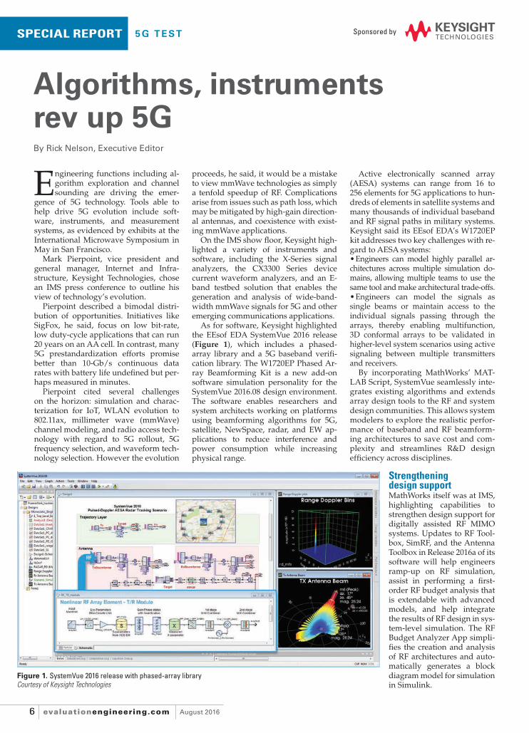
Figure 1. SystemVue 2016 release with phased-array libraryCourtesy of Keysight Technologies
Engineering functions including al-gorithm exploration and channel sounding are driving the emer-
gence of 5G technology. Tools able to help drive 5G evolution include soft-ware, instruments, and measurement systems, as evidenced by exhibits at the International Microwave Symposium in May in San Francisco.
Mark Pierpoint, vice president and general manager, Internet and Infra-structure, Keysight Technologies, chose an IMS press conference to outline his view of technology’s evolution.
Pierpoint described a bimodal distri-bution of opportunities. Initiatives like SigFox, he said, focus on low bit-rate, low duty-cycle applications that can run 20 years on an AA cell. In contrast, many 5G prestandardization efforts promise better than 10-Gb/s continuous data rates with battery life undefi ned but per-haps measured in minutes.
Pierpoint cited several challenges on the horizon: simulation and charac-terization for IoT, WLAN evolution to 802.11ax, millimeter wave (mmWave) channel modeling, and radio access tech-nology with regard to 5G rollout, 5G frequency selection, and waveform tech-nology selection. However the evolution
proceeds, he said, it would be a mistake to view mmWave technologies as simply a tenfold speedup of RF. Complications arise from issues such as path loss, which may be mitigated by high-gain direction-al antennas, and coexistence with exist-ing mmWave applications.
On the IMS show fl oor, Keysight high-lighted a variety of instruments and software, including the X-Series signal analyzers, the CX3300 Series device current waveform analyzers, and an E-band testbed solution that enables the generation and analysis of wide-band-width mmWave signals for 5G and other emerging communications applications.
As for software, Keysight highlighted the EEsof EDA SystemVue 2016 release (Figure 1), which includes a phased-array library and a 5G baseband verifi -cation library. The W1720EP Phased Ar-ray Beamforming Kit is a new add-on software simulation personality for the SystemVue 2016.08 design environment. The software enables researchers and system architects working on platforms using beamforming algorithms for 5G, satellite, NewSpace, radar, and EW ap-plications to reduce interference and power consumption while increasing physical range.
Active electronically scanned array (AESA) systems can range from 16 to 256 elements for 5G applications to hun-dreds of elements in satellite systems and many thousands of individual baseband and RF signal paths in military systems. Keysight said its EEsof EDA’s W1720EP kit addresses two key challenges with re-gard to AESA systems:
•Engineers can model highly parallel ar-chitectures across multiple simulation do-mains, allowing multiple teams to use the same tool and make architectural trade-offs.
•Engineers can model the signals as single beams or maintain access to the individual signals passing through the arrays, thereby enabling multifunction, 3D conformal arrays to be validated in higher-level system scenarios using active signaling between multiple transmitters and receivers.
By incorporating MathWorks’ MAT-LAB Script, SystemVue seamlessly inte-grates existing algorithms and extends array design tools to the RF and system design communities. This allows system modelers to explore the realistic perfor-mance of baseband and RF beamform-ing architectures to save cost and com-plexity and streamlines R&D design effi ciency across disciplines.
Strengthening design supportMathWorks itself was at IMS, highlighting capabilities to strengthen design support for digitally assisted RF MIMO systems. Updates to RF Tool-box, SimRF, and the Antenna Toolbox in Release 2016a of its software will help engineers ramp-up on RF simulation, assist in performing a fi rst-order RF budget analysis that is extendable with advanced models, and help integrate the results of RF design in sys-tem-level simulation. The RF Budget Analyzer App simpli-fi es the creation and analysis of RF architectures and auto-matically generates a block diagram model for simulation in Simulink.
SPECIAL REPORT 5G TEST Sponsored by
Algorithms, instruments rev up 5GBy Rick Nelson, Executive Editor
06-09_EE_201608_SpecialReport_5G_FINAL_eb.indd 606-09_EE_201608_SpecialReport_5G_FINAL_eb.indd 6 7/7/2016 4:16:58 PM7/7/2016 4:16:58 PM
evaluationengineering.comAugust 2016 7
S PE C I A L R E P O R T - 5 G T E S T
Ken Karnofsky, senior strategist, sig-nal processing, outlined some of the challenges and MathWorks’ approach to meeting them. Innovation drivers, he said, include ultrahigh throughput, massive connectivity for IoT, and de-vice integration—all of which must be achieved in the face of accelerating product cycles. One result is a change in the need for particular engineering roles and skills.
Next-generation wireless designs, Karnofsky said, require at least seven different skills in the areas of system architecture design, DSP algorithm exploration, software development, digital-hardware design, mixed-signal design, RF design, and antenna design. MATLAB and Simulink, he said, span these areas from system architecture investigations through prototyping and product implementation. The software supports rapid and fl exible algorithm exploration, design, and analysis while enabling unifi ed simulation of digital, RF, and antenna elements.
Karnofsky outlined 5G requirements, including better than 20-Gb/s data rates, less than 10-ms latency, and LTE/WAN
coexistence. Candidate technologies in-clude massive MIMO and beamforming, active phased-array antennas, and new waveforms, including UFMC, FBMC, and GFDM. Candidate waveforms, Karnofsky said, can be defi ned and evaluated using MATLAB, with the goals of minimizing interference, assessing the impact of digi-tal and hybrid beamforming techniques, and modeling and assessing the impact of antenna confi gurations. He described Er-icsson’s use of MathWorks tools to devel-op an FPGA-based 5G testbed employing beamforming algorithms for multi-user MIMO, achieving 25-Gb/s data rates in a fi eld trial.
mmWave transceiverNational Instruments highlighted a number of innovations at IMS, includ-ing advanced mmWave technology for channel sounding and 5G prototyping as well as advanced solutions for RFIC test from lab-based characterization systems to high-volume manufacturing test solutions using the NI Semiconduc-tor Test System.
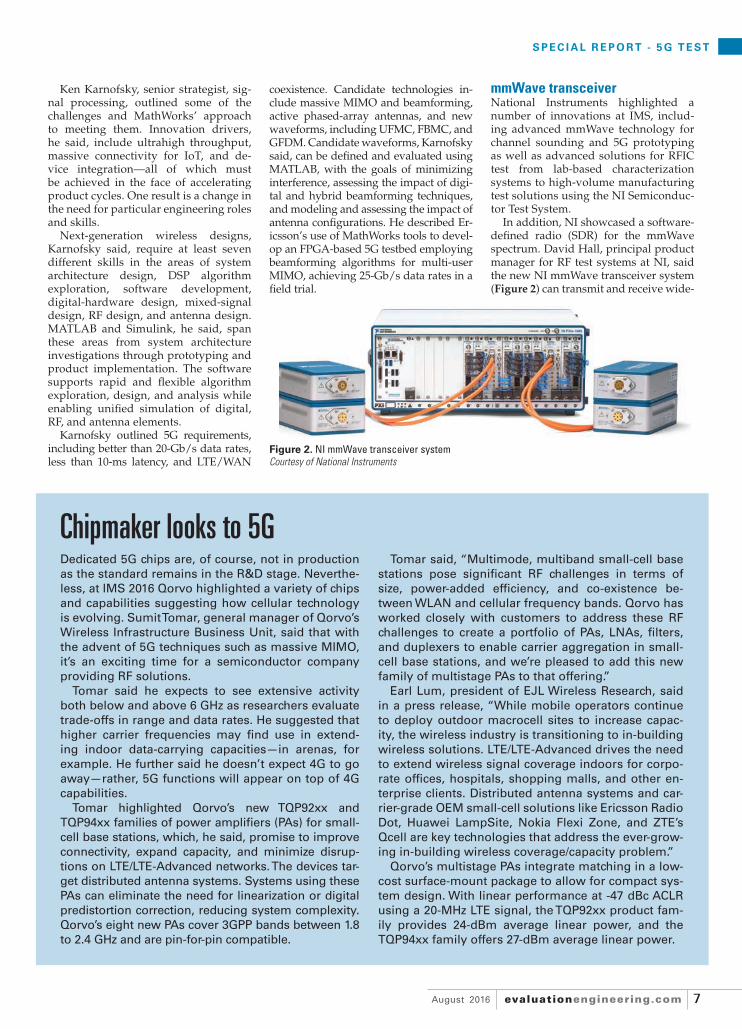
In addition, NI showcased a software-defi ned radio (SDR) for the mmWave spectrum. David Hall, principal product manager for RF test systems at NI, said the new NI mmWave transceiver system (Figure 2) can transmit and receive wide-
Figure 2. NI mmWave transceiver systemCourtesy of National Instruments
Chipmaker looks to 5GTomar said, “Multimode, multiband small-cell base
stations pose signifi cant RF challenges in terms of
size, power-added effi ciency, and co-existence be-
tween WLAN and cellular frequency bands. Qorvo has
worked closely with customers to address these RF
challenges to create a portfolio of PAs, LNAs, fi lters,
and duplexers to enable carrier aggregation in small-
cell base stations, and we’re pleased to add this new
family of multistage PAs to that offering.”
Earl Lum, president of EJL Wireless Research, said
in a press release, “While mobile operators continue
to deploy outdoor macrocell sites to increase capac-
ity, the wireless industry is transitioning to in-building
wireless solutions. LTE/LTE-Advanced drives the need
to extend wireless signal coverage indoors for corpo-
rate offi ces, hospitals, shopping malls, and other en-
terprise clients. Distributed antenna systems and car-
rier-grade OEM small-cell solutions like Ericsson Radio
Dot, Huawei LampSite, Nokia Flexi Zone, and ZTE’s
Qcell are key technologies that address the ever-grow-
ing in-building wireless coverage/capacity problem.”
Qorvo’s multistage PAs integrate matching in a low-
cost surface-mount package to allow for compact sys-
tem design. With linear performance at -47 dBc ACLR
using a 20-MHz LTE signal, the TQP92xx product fam-
ily provides 24-dBm average linear power, and the
TQP94xx family offers 27-dBm average linear power.
Dedicated 5G chips are, of course, not in production
as the standard remains in the R&D stage. Neverthe-
less, at IMS 2016 Qorvo highlighted a variety of chips
and capabilities suggesting how cellular technology
is evolving. Sumit Tomar, general manager of Qorvo’s
Wireless Infrastructure Business Unit, said that with
the advent of 5G techniques such as massive MIMO,
it’s an exciting time for a semiconductor company
providing RF solutions.
Tomar said he expects to see extensive activity
both below and above 6 GHz as researchers evaluate
trade-offs in range and data rates. He suggested that
higher carrier frequencies may fi nd use in extend-
ing indoor data-carrying capacities—in arenas, for
example. He further said he doesn’t expect 4G to go
away—rather, 5G functions will appear on top of 4G
capabilities.
Tomar highlighted Qorvo’s new TQP92xx and
TQP94xx families of power amplifi ers (PAs) for small-
cell base stations, which, he said, promise to improve
connectivity, expand capacity, and minimize disrup-
tions on LTE/LTE-Advanced networks. The devices tar-
get distributed antenna systems. Systems using these
PAs can eliminate the need for linearization or digital
predistortion correction, reducing system complexity.
Qorvo’s eight new PAs cover 3GPP bands between 1.8
to 2.4 GHz and are pin-for-pin compatible.
06-09_EE_201608_SpecialReport_5G_FINAL_eb.indd 706-09_EE_201608_SpecialReport_5G_FINAL_eb.indd 7 7/7/2016 4:17:13 PM7/7/2016 4:17:13 PM
August 2016evaluationengineering.com8
is used as the sounding signal source. The R&S FSW operates as a receiver and can be employed with various frequen-cies and bandwidths. The R&S FSW85, for example, enables users to analyze sounding signals up to 85 GHz without an external mixer. Adding the R&S FSW-B2000 option extends the possible analy-sis bandwidth to 2 GHz.
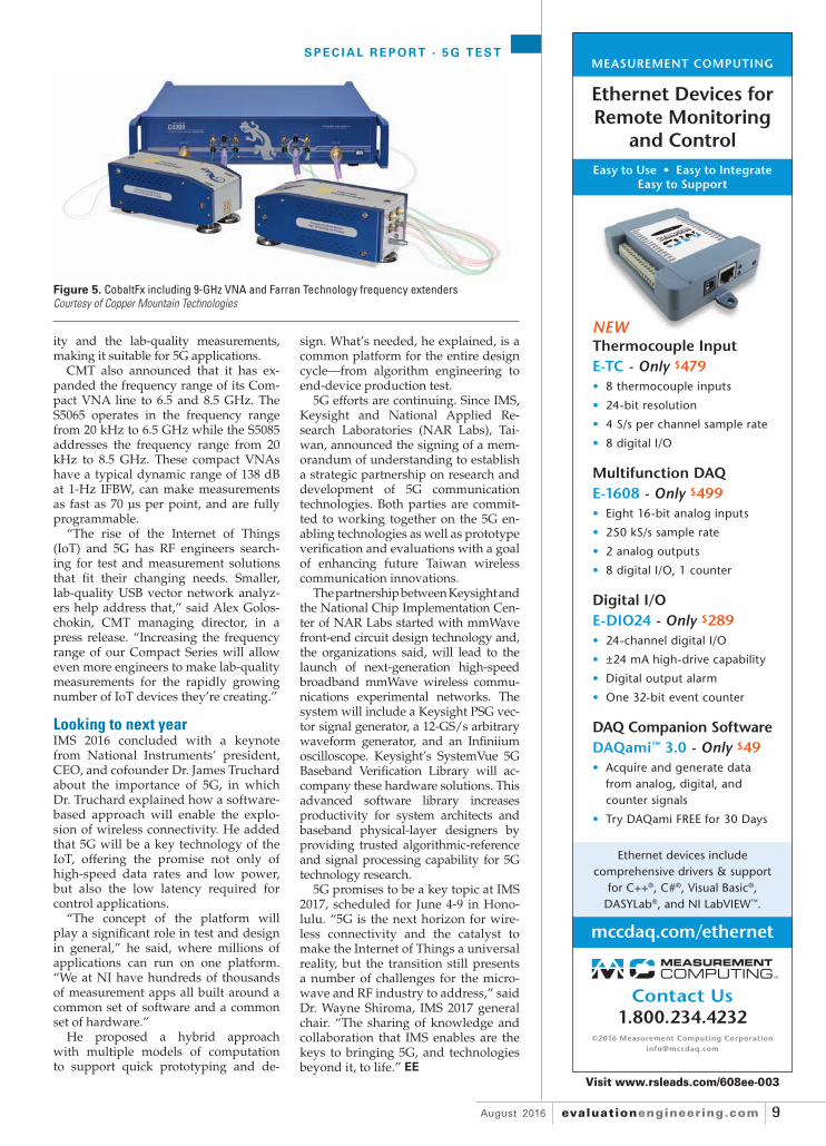
Vector network analyzersAnritsu showcased its high-frequency test instruments that address the challenges associated with emerging microwave and mmWave technologies, including 5G. The company highlighted its VectorStar and ShockLine (Figure 4) vector network ana-lyzer (VNA) families, both of which fea-ture Anritsu’s patented nonlinear trans-mission line technology. The company demonstrated a measurement system fea-turing the VectorStar MS4640B VNA and the MG3710A RF signal generator that conducted modulated measurements, with the VNA confi gured with 200 MHz of instantaneous bandwidth. Anritsu ex-hibited the E-band option for its Shock-Line MS46522B two-port VNA, which can make accurate measurements from 55 to 92 GHz in manufacturing environments.
Anritsu also highlighted a new eye-diagram option for VectorStar; the op-tion can help SI engineers responsible for the design of high-speed data transmis-sion requirements necessary for emerg-ing systems such as 5G. The new Eye Diagram option updates the VectorStar display via a trace-based process rather than a con-ventional fi le-based meth-od, eliminating the need to manually transfer .SnP fi les. Unlike other VNAs, there is no need to store the S-parameter performance in a fi le and then recall the fi le to observe the eye diagram. The company said the op-tion improves measurement
SPECIAL REPORT 5G TEST Sponsored by
bandwidth signals at a 2-GHz real-time bandwidth, covering the spectrum in the E-band, 71 to 76 GHz. Engineers and scientists have used SDRs in the spec-trum below 6 GHz for years. However, Hall said, with companies investing in mmWave as a potential core technology for 5G, researchers now have a full-fea-tured SDR platform to drive initiatives based on this technology.
The mmWave transceiver system in-cludes new PXI Express modules that collectively function as an mmWave ac-cess point for a user device. Because of the transceiver’s fl exibility, users can de-velop mmWave communication proto-typing systems or perform channel mea-surements using the same system.
The mmWave baseband software delivers a complete mmWave physi-cal layer including channel coding in LabVIEW virtual instrument source code to expedite system development while alleviating many of the system integration tasks. Researchers also can use the mmWave transceiver system baseband with the E-band mmWave heads or other third-party RF front ends to offer maximum flexibility for exploring other mmWave and micro-wave frequency bands.
According to Hall, 5G will undoubt-edly include frequencies above 6 GHz, and the mmWave transceiver system will assist in understanding the propagation models of higher frequency signals and building real-world prototypes.
Hall said that Nokia, as a key partici-pant in NI’s RF/Communications Lead User program, has been working with early versions of the mmWave trans-ceiver system in its 5G research initia-tives for more than a year. Tod Sizer, head of mobile radio research for Nokia Bell Labs, said in a press release, “NI’s mmWave transceiver system has been a key research platform for our mmWave research. The platform delivers the right combination of hardware and software necessary to expedite our research and has given us confi dence that mmWave will indeed be a critical technology for 5G.” He added that at this year’s Brook-lyn 5G Summit in April Nokia demon-strated a high-data-rate mmWave system using a phased array at 60 GHz using NI’s platform.
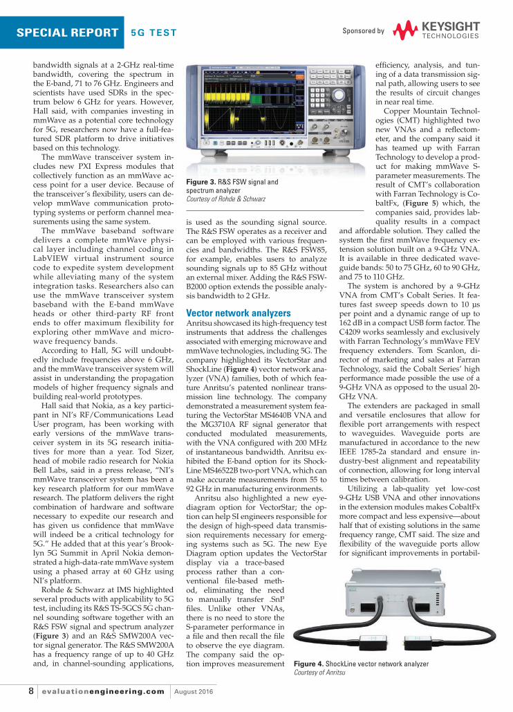
Rohde & Schwarz at IMS highlighted several products with applicability to 5G test, including its R&S TS-5GCS 5G chan-nel sounding software together with an R&S FSW signal and spectrum analyzer (Figure 3) and an R&S SMW200A vec-tor signal generator. The R&S SMW200A has a frequency range of up to 40 GHz and, in channel-sounding applications,
Figure 3. R&S FSW signal and spectrum analyzerCourtesy of Rohde & Schwarz
effi ciency, analysis, and tun-ing of a data transmission sig-nal path, allowing users to see the results of circuit changes in near real time.
Copper Mountain Technol-ogies (CMT) highlighted two new VNAs and a refl ectom-eter, and the company said it has teamed up with Farran Technology to develop a prod-uct for making mmWave S-parameter measurements. The result of CMT’s collaboration with Farran Technology is Co-baltFx, (Figure 5) which, the companies said, provides lab-quality results in a compact
and affordable solution. They called the system the fi rst mmWave frequency ex-tension solution built on a 9-GHz VNA. It is available in three dedicated wave-guide bands: 50 to 75 GHz, 60 to 90 GHz, and 75 to 110 GHz.
The system is anchored by a 9-GHz VNA from CMT’s Cobalt Series. It fea-tures fast sweep speeds down to 10 μs per point and a dynamic range of up to 162 dB in a compact USB form factor. The C4209 works seamlessly and exclusively with Farran Technology’s mmWave FEV frequency extenders. Tom Scanlon, di-rector of marketing and sales at Farran Technology, said the Cobalt Series’ high performance made possible the use of a 9-GHz VNA as opposed to the usual 20-GHz VNA.
The extenders are packaged in small and versatile enclosures that allow for fl exible port arrangements with respect to waveguides. Waveguide ports are manufactured in accordance to the new IEEE 1785-2a standard and ensure in-dustry-best alignment and repeatability of connection, allowing for long interval times between calibration.
Utilizing a lab-quality yet low-cost 9-GHz USB VNA and other innovations in the extension modules makes CobaltFx more compact and less expensive—about half that of existing solutions in the same frequency range, CMT said. The size and fl exibility of the waveguide ports allow for signifi cant improvements in portabil-
Figure 4. ShockLine vector network analyzerCourtesy of Anritsu
06-09_EE_201608_SpecialReport_5G_FINAL_eb.indd 806-09_EE_201608_SpecialReport_5G_FINAL_eb.indd 8 7/7/2016 4:17:28 PM7/7/2016 4:17:28 PM
evaluationengineering.comAugust 2016 9
S PE C I A L R E P O R T - 5 G T E S T
Figure 5. CobaltFx including 9-GHz VNA and Farran Technology frequency extendersCourtesy of Copper Mountain Technologies
ity and the lab-quality measurements, making it suitable for 5G applications.
CMT also announced that it has ex-panded the frequency range of its Com-pact VNA line to 6.5 and 8.5 GHz. The S5065 operates in the frequency range from 20 kHz to 6.5 GHz while the S5085 addresses the frequency range from 20 kHz to 8.5 GHz. These compact VNAs have a typical dynamic range of 138 dB at 1-Hz IFBW, can make measurements as fast as 70 μs per point, and are fully programmable.
“The rise of the Internet of Things (IoT) and 5G has RF engineers search-ing for test and measurement solutions that fi t their changing needs. Smaller, lab-quality USB vector network analyz-ers help address that,” said Alex Golos-chokin, CMT managing director, in a press release. “Increasing the frequency range of our Compact Series will allow even more engineers to make lab-quality measurements for the rapidly growing number of IoT devices they’re creating.”
Looking to next yearIMS 2016 concluded with a keynote from National Instruments’ president, CEO, and cofounder Dr. James Truchard about the importance of 5G, in which Dr. Truchard explained how a software-based approach will enable the explo-sion of wireless connectivity. He added that 5G will be a key technology of the IoT, offering the promise not only of high-speed data rates and low power, but also the low latency required for control applications.
“The concept of the platform will play a signifi cant role in test and design in general,” he said, where millions of applications can run on one platform. “We at NI have hundreds of thousands of measurement apps all built around a common set of software and a common set of hardware.”
He proposed a hybrid approach with multiple models of computation to support quick prototyping and de-
sign. What’s needed, he explained, is a common platform for the entire design cycle—from algorithm engineering to end-device production test.
5G efforts are continuing. Since IMS, Keysight and National Applied Re-search Laboratories (NAR Labs), Tai-wan, announced the signing of a mem-orandum of understanding to establish a strategic partnership on research and development of 5G communication technologies. Both parties are commit-ted to working together on the 5G en-abling technologies as well as prototype verifi cation and evaluations with a goal of enhancing future Taiwan wireless communication innovations.
The partnership between Keysight and the National Chip Implementation Cen-ter of NAR Labs started with mmWave front-end circuit design technology and, the organizations said, will lead to the launch of next-generation high-speed broadband mmWave wireless commu-nications experimental networks. The system will include a Keysight PSG vec-tor signal generator, a 12-GS/s arbitrary waveform generator, and an Infi niium oscilloscope. Keysight’s SystemVue 5G Baseband Verifi cation Library will ac-company these hardware solutions. This advanced software library increases productivity for system architects and baseband physical-layer designers by providing trusted algorithmic-reference and signal processing capability for 5G technology research.
5G promises to be a key topic at IMS 2017, scheduled for June 4-9 in Hono-lulu. “5G is the next horizon for wire-less connectivity and the catalyst to make the Internet of Things a universal reality, but the transition still presents a number of challenges for the micro-wave and RF industry to address,” said Dr. Wayne Shiroma, IMS 2017 general chair. “The sharing of knowledge and collaboration that IMS enables are the keys to bringing 5G, and technologies beyond it, to life.” EE
Ethernet devices includecomprehensive drivers & support
for C++®, C#®, Visual Basic®, DASYLab®, and NI LabVIEW™.
Contact Us1.800.234.4232
mccdaq.com/ethernet
MEASUREMENT COMPUTING
Easy to Use • Easy to IntegrateEasy to Support
Ethernet Devices for Remote Monitoring
and Control
Thermocouple InputE-TC - Only $479• 8 thermocouple inputs
• 24-bit resolution
• 4 S/s per channel sample rate
• 8 digital I/O
NEW
Multifunction DAQE-1608 - Only $499• Eight 16-bit analog inputs
• 250 kS/s sample rate
• 2 analog outputs
• 8 digital I/O, 1 counter
Digital I/OE-DIO24 - Only $289• 24-channel digital I/O
• ±24 mA high-drive capability
• Digital output alarm
• One 32-bit event counter
DAQ Companion SoftwareDAQami™ 3.0 - Only $49• Acquire and generate data from analog, digital, and counter signals
• Try DAQami FREE for 30 Days
©2016 Measurement Computing Corporation [email protected]
Visit www.rsleads.com/608ee-003
06-09_EE_201608_SpecialReport_5G_FINAL_eb.indd 906-09_EE_201608_SpecialReport_5G_FINAL_eb.indd 9 7/7/2016 4:17:41 PM7/7/2016 4:17:41 PM

August 2016evaluationengineering.com10
Figure 1. PXMe7820 high-speed multimeasurement instrumentCourtesy of VX Instruments
Today’s DMM designs are all about increasing a test sys-tem’s capability to comprehensively address diverse ap-plications. For example, because DMMs already need
to make isolated measurements, several manufacturers have added isolated digitizer functionality. This means that the same module can accomplish data acquisition and logging as well as conventional DMM measurements. In another case, DSP-based algorithms are performing RMS computation, but this is just one of the many signal processing jobs that a DSP can do.
In the process of developing DMMs beyond their basic mea-surement roots, trade-offs must be made. Very high measure-ment resolution and accuracy generally imply slower speed. High speed and high input impedance often attract more noise. And, safety clearances and maximum voltage ratings come un-der greater scrutiny as a module’s component density increases to accommodate new features. A manufacturer’s emphasis on certain application areas determines how these and many other performance issues will be balanced in a new design.
Changing the nameTo better describe the mix of capabilities in its PXMe7820 (PXIe interface) instrument, VX Instruments calls it a high-speed multimeasurement device. The company’s Christian Plötz, technical sales engineer, explained, “Our philosophy is to have a digitizer that also is able to be a DMM. So we are thinking in MS/s. [Most] manufacturers of DMMs design a DMM and update the device with digitizer functionality, so they are thinking in reading/s.”
The PXMe7820 functions as a 40-MS/s, 16-bit high-speed digitizer that can handle 250-V peak signals and has a 5-MHz bandwidth. In addition, it is a fully isolated 24-bit resolution DMM that measures inductance, capacitance, and two- and four-wire resistance as well as the usual AC and DC voltage and current. As shown in Figure 1, the typical front-panel ba-nana jacks have been replaced by coaxial connectors to handle high-speed signals.
“Our customers often have the need to realize shorter test times to generate a higher product throughput,” Plötz said. “The PXMe7820 therefore combines high-speed measure-ment and the high-speed inter-facing of PXIe. Furthermore, the combination of different functions in one device reduces the need for additional ele-ments such as cabling and ma-trix units in the test setup. This also can reduce the test times of the application. Moreover,” he continued, “there is a rising de-mand for measurement devices that have a minimum infl uence on the measured signal. That is why we focused on high input impedance.”
VX Instruments produces a number of digitizers, power sup-plies, source-measure units, arbitrary waveform generators, and DMMs. Plötz said that the company’s experience gained
through its digitizer and power supply designs was especially helpful when developing the multimeasurement PXMe7820. In particular, he said, the very low-noise and low capacitance to ground of the power supplies that drive the isolated measure-ment circuitry are key to high AC accuracy.
Pickering Interfaces distributes the PXMe7820 in the United States.
Emphasizing measurement accuracyNational Instruments’ PXIe-4081 DMM (Figure 2) follows on from the earlier PXI-4071 model and continues to focus on mea-surement accuracy. Several factors such as long-term stability, built-in calibration standards, and good thermal design con-tribute to measurement accuracy.
Basic inductance and capacitance measurements are not in-cluded in the 4081. Instead, they are available on NI’s PXIe-4082, a 6½-digit instrument with reduced specifi cations compared to the 4081: 1-A maximum current rather than 3 A, 300-V maximum voltage rather than 1,000 V, and 25 ppm of reading + 6 ppm voltage accuracy on the 10-V range vs. 12 ppm + 0.5 ppm.
According to Mike Watts, product manager-modular instruments at the company, “The PXIe-4081 7½-digit DMM builds on the technol-ogy used in the PXI-4071 DMM, using a unique combination of off-the-shelf high-speed ADC technology and a custom-designed sigma-delta converter to provide the noise, linearity, and speed performance required to achieve high-speed and high-precision measurements in a single instrument. Additionally, the PXIe-4081 DMM uses one of the most stable onboard voltage references available, Linear Technology’s LTZ1000 Ultra Precision Reference, to provide stable performance across temperature and time.”
Having an accurate onboard voltage reference certainly makes calibration convenient, but including a good reference and actually achieving the best possible performance from it are two different things. The LTZ1000 datasheet identifi es some of the possible pitfalls.
Small temperature differences can generate error voltages that are signifi cant compared to the reference’s basic speci-fi cations. One way this occurs is through the thermocouples formed when the device’s Kovar leads are soldered to copper PCB traces and via the thermocouples inherent in resistors and other associated components. In addition, mechanical stresses caused by temperature differences or because of the way a PCB has been mounted can change the reference output.
A design that successfully avoids degrading the voltage ref-erence accuracy provides several benefi ts. Obviously, the DMM accuracy can be directly linked to that of the reference. Beyond that, a reference with long-term stability implies that a DMM requires less frequent external calibration. In a white paper, NI
Figure 2. NI-PXIe-4081 7½-digit DMMCourtesy of National Instruments
Sponsored bySPECIAL REPORT M O DUL A R D M M s
DMMs extended and refi nedBy Tom Lecklider, Senior Technical Editor
10-13_EE_201608_SpecialReport_ModularDMMs_FINAL_eb.indd 1010-13_EE_201608_SpecialReport_ModularDMMs_FINAL_eb.indd 10 7/7/2016 1:56:20 PM7/7/2016 1:56:20 PM

Ready to achieve MVP status? Go to the Scopes Learning Center:www.keysight.com/find/ScopeMVP
Keysight In niiVision oscilloscopes 2000 X-Series 3000T X-Series 4000 X-Series 6000 X-Series
Bandwidth 70 MHz – 200 MHz 100 MHz – 1 GHz 200 MHz – 1.5 GHz 1 GHz – 6 GHz
Instrument integration Arbitrary waveform generator, digital voltmeter, protocol analyzer, FFT, counter, MSO
Become your company’s most valuable player.Elevate your status with Keysight’s In niiVision oscilloscopes.Get your projects on the fast track with features such as zone triggering, built-in analysis software and super-fast waveform update rates. Plus Keysight has a team of experts ready and available to help you overcome any test and measurement obstacles. You already have the talent, and with Keysight you have the tools you need to become your company’s MVP.
© Keysight Technologies, Inc. 2016
Buy from an Authorized Distributor:
10-13_EE_201608_SpecialReport_ModularDMMs_FINAL_eb.indd 1110-13_EE_201608_SpecialReport_ModularDMMs_FINAL_eb.indd 11 7/7/2016 12:15:29 PM7/7/2016 12:15:29 PM

August 2016evaluationengineering.com12
Sampling ratio
Using last sample
Using one more sample
Linearly interpolating
9.9 0.707115028 0.707091726 0.707105897
9.955 0.707145561 0.707101900 0.707107558
10.123 0.707113748 0.707091002 0.707105962
Theoretical result 0.707106781
Sponsored bySPECIAL REPORT M O DUL A R D M M s
stated that, “… the PXIe-4081 includes a two-year guaranteed accuracy of 12 ppm to further reduce the cost of test by mini-mizing downtime for instrument calibration.”1
The PXIe-4081 also uses advanced DMM measurement tech-niques such as offset compensated Ohms and higher-order DC noise rejection.
OhmsThe Ohms function in the 4081 forces a current through the unknown resistance and measures the resulting voltage drop across it. Many applications involve not just the resistance in question, but also an accompanying voltage source. Examples given in an NI technical note include switching systems using uncompensated reed relays with Kovar leads (because of the Kovar-copper thermocouple voltage), in-circuit measurements on live power supply conductors, and measuring the resistance of batteries or forward-biased diodes.2
Offset Ohms compensation operates by measuring the volt-age across the unknown resistance one time without any test current and again with test current. In the fi rst measurement, any voltage that is measured is caused by an associated volt-age source. Subtracting that value from the second reading ef-fectively eliminates the voltage source from the measurement.
The technique works well but does have limitations. In the technical note, NI cautions against trying to eliminate offsets larger than 1 V. The offset Ohms compensation mode is intend-ed for use when measuring low resistance values that usually produce a small test voltage. Because the test voltage is small, thermal EMFs can have a signifi cant effect on accuracy.
NoiseNoise rejection typically focuses on reducing contributions at the AC supply frequency and its harmonics. One of the advan-tages of a sigma-delta converter, such as is used in the PXIe-4081, is the noise reduction it provides by bandwidth shaping. As noted in an EE-Evaluation Engineering special report, Analog Devices’ Walt Kester explained that in a sigma-delta ADC, the modulator shapes the noise, ”… so that it lies above the pass-band of the digital output fi lter, and the ENOB [effective num-ber of bits] is therefore much larger than would otherwise be expected from the oversampling ratio.”3
Interestingly, Linear Technology recently released a 24-bit successive approximation ADC that operates at a 2-MS/s rate and includes an integrated digital fi lter capable of performing up to 65,536 averages.4 With this number of averages, the com-pany claims the output achieves a 30.5 reading/s rate with less than 1 LSB of noise at a full 24-bit resolution. Of course, it takes more than an ADC to make a DMM, but it is important that sig-ma-delta ADCs no longer are the only path to high resolution.
The PXIe-4081 digital output fi lter provides additional noise reduction, and in the 4071, three selections are available. Nor-mal DC noise rejection implements a digital fi lter with equal weighting for all samples. This means that transmission nulls occur at frequencies that are integer multiples of the inverse of the ADC aperture period. For example, specifying a 20-ms aperture corresponds to nulls at 50 Hz, 100 Hz, 150 Hz…. This type of noise rejection is similar to that used in DMMs with conventional dual-slope ADCs that typically measured for a number of power line cycles.
Second-order DC noise rejection creates nulls only at even multiples of the inverse of the aperture period, but the nulls are wider and the overall response falls off faster with frequency than for normal DC rejection. This means that the aperture time must be twice as long as with normal DC fi ltering to attenuate the same frequencies.
Finally, high-order DC noise reduction provides more than 100 dB of rejection for frequencies greater than about 4.5/ap-erture time. Using the same 50-Hz example, the aperture time must be at least 90 ms. The high-order fi lter has the benefi t of very large attenuation for any frequency higher than 4.6/aper-ture time, but it does signifi cantly reduce the readings/s rate.
Addressing fi eld operationMarvin Test Solutions’ (MTS) Mike Dewey, director of mar-keting at the company, positioned the MTS GX2065-M DMM (Figure 3) as, “… a rugged, extended temperature version of the GX2065 DMM. Developed to address the demanding en-vironmental conditions associated with portable/fl ightline test applications, the GX2065-M retains the same features and ca-pabilities as the GX2065 but extends the operating and storage temperature ranges. Specifi cally, the GX2065-M is designed to operate from -20°C to +70°C.”
Several of the trade-offs associated with the GX2065 design are discussed in a 2012 Autotestcon paper.5 Rather than using
Excel RMS simulation comparing accuracy of integer vs. noninteger number of samples
Noninteger number of samples improves RMS accuracyA DMM performs uncorrelated sampling because the position
of a sample relative to a cycle of the input frequency is com-
pletely random. RMS measurement accuracy improves as the
number of samples per signal cycle increases, but a signifi cant
error can remain if only integer numbers of samples are used.
Requiring a very large number of samples isn’t practical in a
power monitoring application because determinations need to
be made within only a single cycle or even a half cycle. Instead,
a research paper1 proposes interpolating the zero-crossing
position between the last sample within a cycle and the fi rst
sample of the next cycle. By using a fractional sample period
for the last sample, RMS accuracy can be greatly improved.
To see how this might work, an Excel spreadsheet was used
to model a 3-MS/s sample rate and a 300-kHz maximum input
frequency sine wave. At a 375-readings/s rate, 8,000 samples
could be acquired. A few noninteger sample rate-to-signal fre-
quency relationships close to 10:1 were tried to simulate uncor-
related sampling. In this model, the fi rst sample was aligned
with the beginning of the waveform and was not interpolated.
More generally, the paper discusses treating both the fi rst and
last sample differently to account for their positions relative to
the beginning and end of complete cycles. The table shows the
results of the experiment.
Reference1. Mog, G. E. and Ribeiro, Dr. E. P., “Mean and RMS calculations for sampled periodic signals with non-integer number of samples per period applied to AC energy systems,“ Universidade Federal do Paraná – UFPR, Centro Politécnico da UFPR, Brazil, October 2004.
10-13_EE_201608_SpecialReport_ModularDMMs_FINAL_eb.indd 1210-13_EE_201608_SpecialReport_ModularDMMs_FINAL_eb.indd 12 7/7/2016 12:15:46 PM7/7/2016 12:15:46 PM

S PE C I A L R E P O R T - M O D U L A R D M M s
Figure 3. GX2065-M ruggedized, extended-temperature range DMMCourtesy of Marvin Test Solutions
Visit www.rsleads.com/608ee-005
the 22-bit DC path, AC measure-ments are made by the 3-MS/s, 16-bit isolated digitizer. This ap-proach allows a large number of samples to be acquired for each RMS calculation. The exact details of the RMS algorithm aren’t avail-able, but it obviously increases resolution from the basic 16 bits of each sample to the 6½ digits (22 bits) quoted in the datasheet.
As the paper describes, “The DMM returns raw measurements and stores correction values in-ternally as 64-bit fi xed-point inte-gers. Every DMM measurement requires at least the multiplication of two 64-bit integers and the di-vision of the result by a 64-bit integer. The multiplication … can be done easily and quickly in software, [and] … takes only about 100 clock cycles…. However, … to speed up the [divide] computation, a custom 128-bit by 128-bit division peripheral was created in Verilog and instantiated in the FPGA.”
In another example of hardware/software trade-offs, “… log-ic-based state machines were implemented wherever possible, with interrupts used for servicing the various measurement and communication events.” This approach allowed most tasks to be handled outside of the main processor, such as, “… communicat-ing across the isolation barrier, transferring data to the PCI bus, and reading the PWM outputs from the temperature sensors.”
The paper highlights some of the design considerations nec-essary to support the wide operating temperature range: “For high-temperature operation, careful layout and board cuts are
required to minimize self-heating effects…. The PXI DMM uses the LM399 voltage reference, which includes a built-in, auto-matically controlled heater. For high-temperature operation, the heater’s power dissipation isn’t a problem because it au-tomatically reduces its power consumption. However, at low temperatures, the heater must use the maximum amount of current to bring the voltage reference up to temperature.”
MTS solved the problem of a large current load at start-up by carefully sequencing the power supplies. Only after all of the supplies are operating and the voltage reference is near its fi nal temperature are the analog supply regulators enabled. As the paper explains, “The complete sequence requires about 10 s at room temperature but can require up to 1 minute at -20°C.”
Dewey concluded, “Besides offering the capability to work over an extended temperature range and be rugged enough for por-table applications, we see the need for enhanced functionality. The capability to incorporate digitizing functionality and associated waveform analysis functions helps make the DMM a more useful and capable multifunction measurement instrument. The capabil-ity to measure and analyze waveform amplitudes, frequency, and even spectrums helps to drive down a test system’s footprint.” EE
References1. PXI Express DMMs form foundation for more accurate, smarter test systems, National Instruments, White Paper, April 2016.2. “Offset compensated Ohms,” NI Digital Multimeters Help 3.0, June 2009.3. Lecklider, T., “Taking signals to bits, modularly,” EE-Evaluation Engineer-ing, March 2016, pp. 6-8.4. “24-Bit 2-MSps SAR ADC Achieves 145-dB Dynamic Range,” Linear Technology, News Release, November 2015.5. Dewey, M. and Robins, J., “Incorporating advanced instrumentation capabilities into a PXI digital multimeter instrument,” IEEE Autotestcon Proceedings, 2012.
10-13_EE_201608_SpecialReport_ModularDMMs_FINAL_eb.indd 1310-13_EE_201608_SpecialReport_ModularDMMs_FINAL_eb.indd 13 7/7/2016 12:16:03 PM7/7/2016 12:16:03 PM

August 2016evaluationengineering.com14
DESIGN FOR TEST
Impacting accuracy of chipmaker’s quality testsBy Peter Sarson, Gregor Schatzberger, and Andreas Wild, ams AG
Near the beginning of every chip design project, the de-sign team will have a debate about the trade-off be-tween cost and quality. One of the most vexed ques-
tions tends to be about the value of incorporating dedicated test modes into the circuit design—that is, about adopting a design for test (DFT) approach.
On the one hand, DFT adds design work and increases the die area to accommodate test functionality that is not used in the end application. On the other, DFT can enable more pre-cise and/or more accurate testing of the chip’s characteristics. This enables the manufacturer to improve quality because the performance of each shipped unit can more closely match the device’s specifi cations as documented in the datasheet.
At ams, an automotive-qualifi ed (ISO/TS16949) manufac-turer of analog and mixed-signal semiconductors, quality is of paramount importance, and this gives the company a close-up view of the value of DFT—even in the digital parts of mixed-signal products. This article uses the example of an EEPROM IP block to show how DFT enables more accurate characteriza-tion of the block and the impact that this has on the quality of devices shipped to automotive customers. Figure 1 shows the architecture of an EEPROM bit cell.
cycles. (In a fast bit, the cell programming/erasing voltage is very low.)
Fast bits occur as an inherent feature of the silicon fabrica-tion process. They are created when aluminum in the wet etch contaminates the oxide layer.
The problem for the IC test engineer is that, although these fast bits might work properly when the EEPROM is initially programmed and erased, after multiple cycles, the low pro-gramming voltage will result in the bit cell failing prematurely.
Automotive quality requirements, however, call for zero de-fects in any bit cells in any EEPROM device. So how can the manufacturer guarantee that no single unit will become unpro-grammable before its specifi ed number of write/erase cycles?
The solution is to screen out all dies containing one or more fast bits. And this is where the value of DFT becomes clear.
Figure 2 shows a distribution of dies with fast bits in a wafer. To meet its quality standard, ams must be able to guarantee that devices close to the pass/fail threshold will stay good after the specifi ed minimum number of write/erase cycles.
SOURCELINE
BITLINE
WELL
MP0
MP1
MP2
WORDLINE
Figure 1. The architecture of an EEPROM bit cell
Figure 2. Distribution of fast bits within a wafer
Volt1stEraseBitA/MEAS_DIR_VI16
10 0 0 0 01 1 12 3 2 33 6 4832 22
45 5675
144
312
748
1152
0
FAST bit devicePotential Fast
bit device
1152
800
400
0
8 9 10 11
EEPROMs: the determinants of qualityFor the user of an EEPROM, a type of nonvolatile memory, quality normally is specifi ed in the following terms:
• the number of write/erase cycles it can support, and •the length of time it can retain data. A typical requirement is for
10 years’ data retention. These quality measures are, in turn, determined by three
characteristics of an EEPROM die: •endurance loops (the number of write operations the EEPROM
can withstand before it can no longer be programmed), • the input voltage at which a bit cell can be programmed and
erased, and •the charge held in a bit cell after a write operation.The bit cell charge is important because, over time, charge
leaks from a programmed cell. The initial charge when pro-grammed must be suffi ciently high to allow for this leakage while still guaranteeing the full 10 years’ data retention capa-bility. Likewise, the input voltage when the device is new must be above a certain minimum to guarantee that no fast bits are present and to ensure that a device can withstand n write/erase
Precise characterization of EEPROM devicesFor its foundry customers, ams must be able to characterize production wafers containing EEPROM blocks to fi lter out failed dies and guarantee the lifetime and data retention of known good dies.
As shown above, characterization of an EEPROM die calls for measurements of input voltage and bit cell charge. And in an EEPROM IP block, these measurements can only be captured accurately with dedicated test circuitry routed to a pin (Figure 3).
This DFT circuitry connects the on-chip high-voltage gen-erator in such a way that the voltage needed to program and erase the bit cells may be driven from outside the chip. Once
14-15_EE_201608_DesignforTest_FINAL_eb.indd 1414-15_EE_201608_DesignforTest_FINAL_eb.indd 14 7/7/2016 11:51:45 AM7/7/2016 11:51:45 AM

evaluationengineering.comAugust 2016 15
DESIGN FOR TEST
vices that already had reached the end of their guaranteed operational lifetime.
These dies then were baked for 4,000 hours at 250°C. According to the standard Arrhenius equation, this is equivalent to 10 years’ operation at 150°C. After this da-ta-retention bake, the dies were tested to check for drift in the bit cell current. If the cell current was found to have drifted by less than 1 μA, data retention would have been verifi ed. It turned out that all failures were actually triggered within the fi rst 24 hours of baking.
If data programmed on the last write operation of the most marginal device can be retained for 10 years, then the data re-tention capability of every other known good die can be confi dently guaranteed.
Transferring the development test method to productionWith the DFT circuitry embedded in the EEPROM IP, the fabrication plant at ams now can characterize every cell in every die in the way described above to screen out fast bit dies. Using the test method outlined here, known good dies with cell current and input voltage values exceed-ing the minimum threshold may be guar-anteed for any number of write/erase cycles and any data retention interval
specifi ed by the user of the EEPROM IP block.The production test method includes a 24-hour bake at 250°C,
after which dies showing a cell current drift of more than 1 μA are rejected.
With this characterization program in place, more than 10 mil-lion EEPROMs, containing some 300 billion bit cells, have been produced, tested, and shipped to customers. The guarantee of quality supported by this production testing regime has been verifi ed in practice: Not a single device has been returned from a customer, suggesting no failures have been found in the fi eld.
ams could not have verifi ed its test method with suffi cient confi dence, nor as accurately identifi ed marginal bad devices, without the test modes implemented in the EEPROM IP block’s circuitry. This provides real-world proof of the value of imple-menting a DFT approach from the outset of a new chip design.
About the authorsPeter Sarson, the test development manager for the Full Service Foundry business unit at ams AG, began his 15-year semiconductor industry career in 2000 when he joined the LTX Applications Engi-neering Group. He received his Chartered Engineer Status from IET in 2003 and his Chartered Manager status in 2014. Sarson holds a Bachelor of Engineering degree in Electrical and Electronic Engineer-ing from The University of Sheffi eld.
Gregor Schatzberger is principal analog designer at ams AG. He joined the company in 1998 and since then performed various roles within the BaseIP group of ams. Schatzberger has several patents and has written several papers. He holds a degree in Electronic Engineer-ing from the Technical University of Graz, Austria.
Andreas Wild has been working as marketing manager for foundry services and technologies in the Full Service Foundry at ams since 2003 and also is responsible for customers in the United States and southern Europe. He began his career in semiconductors in 1995 as an administrator responsible for the product engineering laboratory at Austria Mikro Systeme International AG. Wild holds a high school diploma in electronics. EE
MEM BLOCK
DATA LINE B
MEM BLOCK
DATA LINE
140130
150160
LATCH SAOUT
SENSEAMP
MP0 MN2 MP1 MN3
MN4MN1
MP3
MN
5M
P4M
N6
180
170
SAENSAENB
SAENDB
TM1
IREF
TM2
MN3 MN0
the bit cell is programmed or erased, the bit cell current can be measured on the same pin, accurate to within a few nanoamps. If the charge is below the minimum threshold for guaranteed lifetime, the device will be failed.
This DFT method guarantees that every bit cell in every chip in every wafer will be tested with the same input voltage. By contrast, in the absence of the dedicated test circuitry, the test routine would use the device’s internal charge pump to gener-ate the voltage, and because of process variation, this voltage will vary from one die to another. As a result, the test results will be subject to a degree of uncertainty: A bit cell with a low charge might be a failure in its own right—or it might have been exposed to too low a programming voltage.
The DFT mode implemented by ams eliminates this source of uncertainty, vastly improving the test quality of this block.
Once all bit cells have been programmed or erased, a digital check can be initialized by sourcing an external reference cur-rent to the external test-mode pin. The sense amplifi er (Figure 3) compares the reference current to the current at the bit cell: If the bit cell current is greater than the reference, a digital high is sent; if the bit cell current is smaller than the reference, a digi-tal low is sent. This produces a digital pattern to verify that all bits are programmed or erased correctly, which may be used to quickly check operation of the device.
Characterizing the device for productionThe test mode built into the IP block, then, provides for accurate measurement of the crucial input voltage and cell current pa-rameters, enabling ams to reject dies containing fast bits.
The question then becomes, how can ams guarantee 10 years’ data retention in dies that pass the input voltage and charge tests?
To do so, it tested the performance of dies near the threshold of rejection as a fast bit. It exercised these dies with the maxi-mum number of endurance loops the device was specifi ed to withstand. This gave the test engineers a set of marginal de-
Figure 3. The DFT circuit implemented in EEPROM IP blocks provided by the ams Full Service Foundry
14-15_EE_201608_DesignforTest_FINAL_eb.indd 1514-15_EE_201608_DesignforTest_FINAL_eb.indd 15 7/7/2016 11:52:06 AM7/7/2016 11:52:06 AM
August 2016evaluationengineering.com16
ADDITIVE MANUFACTURING
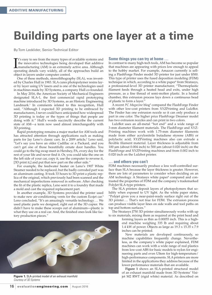
Figure 1. SLA-printed model of an exhaust manifoldCourtesy of 3D Systems
It’s easy to see from the many types of available systems and the innovative technologies being developed that additive manufacturing (AM) is an extremely active area. Although
operating details vary widely, all of the approaches build an object in layers under computer control.
One of these methods, stereolithography (SLA), was invent-ed by Charles Hull in 1983. SLA cures photopolymer resins lay-er by layer using UV lasers and is one of the technologies used in machines made by 3D Systems, a company Hull co-founded.
In May 2016, the American Society of Mechanical Engineers designated SLA-1, the fi rst commercial rapid prototyping machine introduced by 3D Systems, as an Historic Engineering Landmark.1 In comments related to this recognition, Hull said, “Although I expected 3D printing to be embraced by manufacturers, I never could have anticipated how widespread 3D printing is today or the types of things that people are doing with it.” Hull’s words succinctly describe the current state of AM—a term now used almost interchangeably with 3D printing.
Rapid prototyping remains a major market for AM tools and has attracted attention through applications such as making parts for Jay Leno’s classic cars. In a 2009 article,2 Leno said, “Let’s say you have an older Cadillac or a Packard, and you can’t get one of those beautifully ornate door handles. You could go to the big swap meet in Hershey, PA, every day for the rest of your life and never fi nd it. Or, you could take the one on the left side of your car, copy it, use the computer to reverse it, [3D print it,] and put that new part on the other side.”
For example, the feedwater heater on Leno’s 1907 White Steamer needed to be replaced, but the badly corroded part was an aluminum casting. It took 33 hours to 3D print a plastic rep-lica of the original, which previously had been scanned and the mechanical imperfections removed in software. After checking the fi t of the plastic replica, Leno sent it to a foundry that made a mold and cast the required replacement part.
In another example, 3D Systems provided the printer used to make new air-conditioning vents for the custom Ecojet car.3 Leno concluded, “It’s an amazingly versatile technology…. We used plastic parts we designed, right out of the 3D copier. We didn’t have to make these scoops out of aluminum—plastic is what they use on a real car. And, the fi nished ones look like fac-tory production pieces.”
Some things you can try at home …In contrast to many high-tech tools, AM has become so popular that machines are appearing with prices low enough to appeal to the hobby market. For example, Amazon currently is sell-ing a FlashForge Finder model 3D printer for just under $500. This type of printer uses the fused deposition modeling (FDM) technique in which, according to a white paper4 from Stratasys, a professional-level 3D printer manufacturer, “Thermoplastic fi lament feeds through a heated head and exits, under high pressure, as a fi ne thread of semi-molten plastic. In a heated chamber, this extrusion process lays down a continuous bead of plastic to form a layer.”
A recent PC Magazine blog5 compared the FlashForge Finder with other low-cost printers from XYZPrinting and LulzBot. The Finder has one extrusion nozzle so it can only produce a part in one color. The higher price FlashForge Dreamer model has two extrusion nozzles and can print in two colors.
LulzBot uses an all-metal “hot end” and a wide range of 3-mm diameter fi lament materials. The FlashForge and XYZ-Printing machines work with 1.75-mm diameter fi laments made from either acrylonitrile butadiene styrene (ABS) or polylactic acid; XYZPrinting machines also can extrude a fl exible fi lament material. Layer thickness is adjustable from 100 μm (about 0.004 inch) to 500 μm (about 0.020 inch) on the FlashForge and XYZPrinting machines and from 0.002 inch to 0.020 inch on the Lulzbot printer.
… and others you can’tFDM machines necessarily produce a less well-controlled sur-face than SLA because the layer thickness is greater. However, there are lots of parameters to consider when deciding on an AM technology. A Stratasys white paper4 compared and con-trasted the properties of FDM and the company’s trademarked PolyJet SLA-type printers.
The SLA printers deposit layers of photopolymers that so-lidify when exposed to UV light. As the white paper states, “Polyjet gives you a near-paint-ready surface right out of the 3D printer…. That’s not true for FDM. The extrusion process can produce visible layer lines on side walls and tool paths on top and bottom surfaces.”
The Stratasys J750 3D printer simultaneously works with up to six materials, mixing them as required at the print head and
forming layers as thin as 0.00055 inch. This is a high-end machine weighing 335 lb and requiring about 1.4 kW of power. Objects as large as 19.3 x 15.35 x 7.9 inches can be printed.
New materials are developed continuously, so machine capabilities frequently change. Neverthe-less, as the company’s white paper explained, FDM machines can work with a wide range of real plastics from low-cost ABS for basic models to nylon for engi-neering parts and even Ultem for high-temperature/high-performance components. SLA printers are more limited in the applications they address because of the lower-performance materials that are available.
Figure 1 shows an SLA-printed structural model of an exhaust manifold made from 3D Systems’ Visi-jet M2 RWT (rigid white) material. As described on
Building parts one layer at a timeBy Tom Lecklider, Senior Technical Editor
16-19_EE_201608_AdditiveManufacturing_FINAL_eb.indd 1616-19_EE_201608_AdditiveManufacturing_FINAL_eb.indd 16 7/7/2016 11:47:15 AM7/7/2016 11:47:15 AM

Launch your calibration to the next level. Get a quote today. www.keysight.com/find/AmericasOneSource
US A: 800 829 4444 CAN: 877 894 4414© Keysight Technologies, Inc. 2016.
Keysight One Source SolutionsSupported Calibrations
Dimensional/Optical Yes
Electrical Yes
Electro-Optics Yes
RF/Microwave Yes
Physical/Mechanical Yes
When you consolidate all your calibration needs with one trusted partner you’ll experience improved performance, increased asset utilization, reduced turnaround time and more success. By supporting Keysight and non-Keysight equipment, no matter how big the problem, or how diverse the test equipment, we’ll help you accomplish your mission.
Before “all systems are go,” all systems need to be good to go.Trust Keysight One Source Solutions for all your calibration needs.
16-19_EE_201608_AdditiveManufacturing_FINAL_eb.indd 1716-19_EE_201608_AdditiveManufacturing_FINAL_eb.indd 17 7/7/2016 11:47:33 AM7/7/2016 11:47:33 AM
August 2016evaluationengineering.com18
ADDITIVE MANUFACTURING
monitor everything from the size of the weld pool [to] tempera-ture and the stability of the laser.”
Todd Rockstroh, a laser processing expert at GE Aviation, commented, “When we designed the nozzle, we wanted to make it from an alloy that was mature, well-known, and thor-oughly tested—nothing exotic.” Cobalt-chromium materials have a long history of successful use in replacement knee and hip joints as well as dental implants. Rockstroh continued, “Be-cause of their medical applications, there has been a tremen-dous amount of research done on these alloys. They are also pretty common because they serve such a large market, which makes them cheaper.”
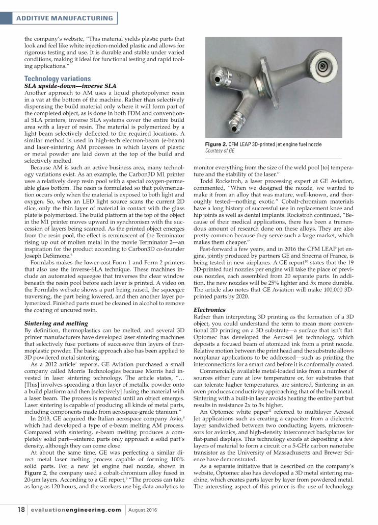
Fast-forward a few years, and in 2016 the CFM LEAP jet en-gine, jointly produced by partners GE and Snecma of France, is being tested in new airplanes. A GE report10 states that the 19 3D-printed fuel nozzles per engine will take the place of previ-ous nozzles, each assembled from 20 separate parts. In addi-tion, the new nozzles will be 25% lighter and 5x more durable. The article also notes that GE Aviation will make 100,000 3D-printed parts by 2020.
ElectronicsRather than interpreting 3D printing as the formation of a 3D object, you could understand the term to mean more conven-tional 2D printing on a 3D substrate—a surface that isn’t fl at. Optomec has developed the Aerosol Jet technology, which deposits a focused beam of atomized ink from a print nozzle. Relative motion between the print head and the substrate allows nonplanar applications to be addressed—such as printing the interconnections for a smart card before it is conformally coated.
Commercially available metal-loaded inks from a number of sources either cure at low temperature or, for substrates that can tolerate higher temperatures, are sintered. Sintering in an oven produces conductivity approaching that of the bulk metal. Sintering with a built-in laser avoids heating the entire part but results in resistance 2x to 3x higher.
An Optomec white paper11 referred to multilayer Aerosol Jet applications such as creating a capacitor from a dielectric layer sandwiched between two conducting layers, microsen-sors for avionics, and high-density interconnect backplanes for fl at-panel displays. This technology excels at depositing a few layers of material to form a circuit or a 5-GHz carbon nanotube transistor as the University of Massachusetts and Brewer Sci-ence have demonstrated.
As a separate initiative that is described on the company’s website, Optomec also has developed a 3D metal sintering ma-chine, which creates parts layer by layer from powdered metal. The interesting aspect of this printer is the use of technology
the company’s website, “This material yields plastic parts that look and feel like white injection-molded plastic and allows for rigorous testing and use. It is durable and stable under varied conditions, making it ideal for functional testing and rapid tool-ing applications.”
Technology variationsSLA upside-down—inverse SLAAnother approach to AM uses a liquid photopolymer resin in a vat at the bottom of the machine. Rather than selectively dispensing the build material only where it will form part of the completed object, as is done in both FDM and convention-al SLA printers, inverse SLA systems cover the entire build area with a layer of resin. The material is polymerized by a light beam selectively defl ected to the required locations. A similar method is used in high-tech electron-beam (e-beam) and laser-sintering AM processes in which layers of plastic or metal powder are laid down at the top of the build and selectively melted.
Because AM is such an active business area, many technol-ogy variations exist. As an example, the Carbon3D M1 printer uses a relatively deep resin pool with a special oxygen-perme-able glass bottom. The resin is formulated so that polymeriza-tion occurs only when the material is exposed to both light and oxygen. So, when an LED light source scans the current 2D slice, only the thin layer of material in contact with the glass plate is polymerized. The build platform at the top of the object in the M1 printer moves upward in synchronism with the suc-cession of layers being scanned. As the printed object emerges from the resin pool, the effect is reminiscent of the Terminator rising up out of molten metal in the movie Terminator 2—an inspiration for the product according to Carbon3D co-founder Joseph DeSimone.6
Formlabs makes the lower-cost Form 1 and Form 2 printers that also use the inverse-SLA technique. These machines in-clude an automated squeegee that traverses the clear window beneath the resin pool before each layer is printed. A video on the Formlabs website shows a part being raised, the squeegee traversing, the part being lowered, and then another layer po-lymerized. Finished parts must be cleaned in alcohol to remove the coating of uncured resin.
Sintering and meltingBy defi nition, thermoplastics can be melted, and several 3D printer manufacturers have developed laser sintering machines that selectively fuse portions of successive thin layers of ther-moplastic powder. The basic approach also has been applied to 3D powdered metal sintering.
As a 2012 article7 reports, GE Aviation purchased a small company called Morris Technologies because Morris had in-vested in laser sintering technology. The article states, “… [This] involves spreading a thin layer of metallic powder onto a build platform and then [selectively] fusing the material with a laser beam. The process is repeated until an object emerges. Laser sintering is capable of producing all kinds of metal parts, including components made from aerospace-grade titanium.”
In 2013, GE acquired the Italian aerospace company Avio,8 which had developed a type of e-beam melting AM process. Compared with sintering, e-beam melting produces a com-pletely solid part—sintered parts only approach a solid part’s density, although they can come close.
At about the same time, GE was perfecting a similar di-rect metal laser melting process capable of forming 100% solid parts. For a new jet engine fuel nozzle, shown in Figure 2, the company used a cobalt-chromium alloy fused in 20-μm layers. According to a GE report,9 “The process can take as long as 120 hours, and the workers use big data analytics to
Figure 2. CFM LEAP 3D-printed jet engine fuel nozzleCourtesy of GE
16-19_EE_201608_AdditiveManufacturing_FINAL_eb.indd 1816-19_EE_201608_AdditiveManufacturing_FINAL_eb.indd 18 7/7/2016 1:59:01 PM7/7/2016 1:59:01 PM

similar to the Aerosol Jet technique. Metal powder simultane-ously is deposited by a spray nozzle and sintered by a high-power laser. This method would appear to require signifi cantly less powdered metal than is used by machines that lay down complete rather than selective layers. The approach also can be used to repair parts.
AM in actionHull’s expectation that 3D printing would revolutionize proto-type production has become reality. Nevertheless, AM involves equipment, processes, and materials that are distinct from con-ventional machining. Training and experience are necessary be-fore you can get the best results. One way that companies can take advantage of 3D printing without much risk is to submit their digital design fi les to a printing bureau.
For example, 3D Systems provides a range of capabilities via the company’s on-demand parts-manufacturing Quickparts 3D design-to-manufacturing service—“the world’s leading provider of unique low-volume and high-volume custom-de-signed parts,” according to the 3D Systems website. If you do not have AM experience, partnering with a company that uses a number of technologies can be an advantage.
On the production side, clusters of 3D printers are being used—in the case of LulzBot, 140 3D printers run for at least 100 hours per week to manufacture parts for more LulzBot printers. According to comments made by Stan Middlekauff, cluster pro-duction supervisor, in an article on the LulzBot website, “The alternative to having [a] cluster producing those parts would be injection molding everything, but the injection molding cost for a die could be thousands of dollars and upward,” Middlekauff
said. “With the cluster now in place, the up-front cost has been paid for us to make any type of part. Plus, if at any moment in time we need to change a part, we can change it quickly.”
AM has revolutionized product development time scales and economics for a wide range of manufacturers. And, it’s being used in production to make parts that can’t be conventionally manufactured as well as provide immediate inventory control. EE
References1. Millsaps, B. B., “Celebrating Chuck Hull & the SLA-1 Original 3D Printer—Now a Historic Mechanical Engineering Landmark,” 3D Print.com, May 19, 2016.2. Leno, J., “Jay Leno’s Printer Replaces Rusty Old Parts,” Popular Me-chanics, June 7, 2009.3. Newman, J., “3D Printing in Leno’s Garage,” Design Engineering Rapid Ready, Dec. 11, 2015.4. “FDM and PolyJet 3D Printing: Determining which technology is right for your application,” Stratasys, Dec. 18, 2015.5. Hoffman, T., “FlashForge Finder 3D Printer,” PC Magazine, April 11, 2016.6. Tilley, A., “How Carbon3D Plans To Transform The Way We Make Stuff,” Forbes, Nov. 23, 2013.7. “GE Is So Stoked About 3D Printing, They’re Using It To Make Parts For Jet Engines,” The Economist, Nov. 24, 2012.8. Milkert, H., “GE Uses Breakthrough New Electron Gun For 3D Printing—10X’s More Powerful Than Laser Sintering,” edprint.com, Aug. 18, 2014.9. Kellner, T., “Joined At The Hip: Where The 3-D Printed Jet Engine Meets The Human Body,” GE Reports, July 1, 2013.10. Gilman, C., “A pragmatic view of additive manufacturing,” GE Global Research, February 2014.11. “Aerosol jet printed electronics overview,” Optomec, May 2009.
ADDITIVE MANUFACTURING
Ensure Performance with EMI ShieldingOur iSeries product line currently offers electromagnetic shielding to preserve signal integrity during operation. From stainless steel fibers, to threaded metal couplings, to all-metal backshells, the iCon and the i2 MX have options to safeguard your signal transmissions.
iSeries connectors feature interchangeable modules and contacts that are universally accepted in all of our connectors. Choose from signal, power, coaxial, fiber, or high speed (VTAC) to help you create the perfect solution for your application.
Our Wire+ Advantage provides engineered, manufactured, and quality tested wire products. Cable assemblies can be terminated to any vendor connector, left as a flying-lead, or configured to be double-ended.
To learn more, visit vpc.com/EE2
Flying Leads
Commercial Connectors
Phone: 540-932-3355 Email: [email protected]
16-19_EE_201608_AdditiveManufacturing_FINAL_eb.indd 1916-19_EE_201608_AdditiveManufacturing_FINAL_eb.indd 19 7/7/2016 11:48:52 AM7/7/2016 11:48:52 AM

August 2016evaluationengineering.com20
SALARY SURVEY
Taking the pulse of the industryBy Tom Lecklider, Senior Technical Editor
In this presidential election year, we’re getting plenty of confl icting informa-tion from numerous political polls.
Even with the great care taken by profes-sional pollsters, it’s still not possible to assume that a small difference pro or con actually has statistical signifi cance. Such uncertainty usually is assigned to the 2% to 3% margin of error that typically exists.
The average engineering salaries for the last three years, derived from reader responses to the annual EE-Evaluation Engineering salary survey, are shown in Table 1. Essentially, the average engi-neering salary has remained fl at from year to year with changes less than ±2%—well within the margin of er-ror. One respondent said, “I have not had any salary increase in more than 10 years,” seeming to confi rm the data. At the other extreme, another said, “… this last year has been the best in eight years for salary increases.” Of the responses received, this view defi nitely was in the minority. About three-quarters of the respondents indicated that they had re-ceived either no raise or a small one in the previous year, with only 22% getting an increase greater than 4%.
While salaries haven’t altered much, this year’s survey responses confi rm trends seen in earlier years. For ex-ample, no doubt we’ve all read about a company’s desire for 20-year-old new employees who also have 15 years of rel-evant experience. One older respondent recounted, “I was sitting in an interview, when the interviewer said: ‘I’m sorry, but we’re looking for someone with current knowledge of the state-of-the-art engi-neering technology, someone who’s re-cently graduated from college.’” In spite of having taught engineering courses at the university level, the respondent did not get the job and concluded that the company actually was saying that, “…
we don’t want to hire someone with years of experience because we’d have to pay them more.”
As shown in Table 2, salary clearly in-creases with years of experience. In the table, the percentage columns represent the respondents within each category. A similar relationship between salary and the number of years spent with one employer can be shown, although as happened in 2014, salaries can level off or drop slightly for respondents who work a long time at the same company.
Location, education, and appsJob responsibility and technical skills as well as your location may be as impor-
Mountain
$119,910
Central
Southeast
Northeast
$98,233
$102,768$109,750
$95,000InternationalInternational
$78,000$78,000
Pacifi c
Figure 1. Average salary vs. location
Years of Experience in the Industry
2016 2015 2014
More than 30 years $111,541 50% $115,073 55% $106,854 46%
25 - 29 $107,187 18% $108,167 15% $117,183 16%
20 - 24 $107,500 14% $97,130 8% $108,356 14%
15 - 19 $95,455 8% $99,405 10% $103,900 6%
10-14 $79,750 4% $87,188 6% $95,385 8%
6-9 $63,750 2% $48,125 3% $83,214 4%
3-5 $75,625 3% $68,750 1% $72,500 3%
Less than 3 $70,833 1% $83,125 3% $78,929 2%
Year Average Salary Percent of Change
2014 $104,914 ----
2015 $106,800 +1.798%
2016 $105,131 -1.562%
To better understand the survey data, the cumulative dollar-percentage for each of the last three years was plotted against a range of salaries. The results showed that the percentage of total re-spondent pay falling within either the lower or higher $50,000-band of salaries was virtually the same for all three years. What variation in average salary there has been occurred because of differ-ences in the salaries from about $90,000 to $150,000. This means that conclusions drawn from the survey data have not been skewed by responses from a large number of highly paid managers one year or from many less-well-paid techni-cians another year.
Table 1. Average salary and changes
Table 2. Salary vs. years of experience in the industry
10%33%
12%22%4%
19%
20-23_EE_201608_SalarySurvey_DUM_eb.indd 2020-23_EE_201608_SalarySurvey_DUM_eb.indd 20 7/8/2016 11:54:55 AM7/8/2016 11:54:55 AM
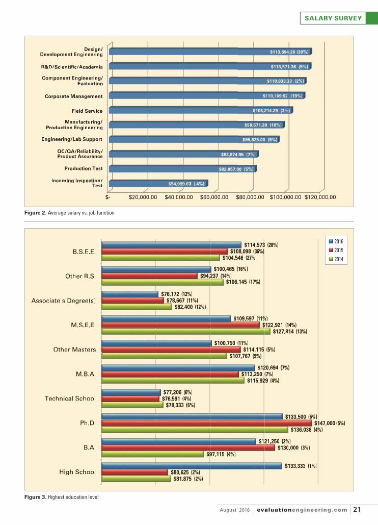
evaluationengineering.comAugust 2016 21
SALARY SURVEY
Figure 2. Average salary vs. job function
$- $20,000.00 $40,000.00 $60,000.00 $80,000.00 $100,000.00 $120,000.00
Incoming Inspection/Test
Production Test
QC/QA/Reliability/Product Assurance
Engineering/Lab Support
Manufacturing/Production Engineering
Field Service
Corporate Management
Component Engineering/Evaluation
R&D/Scientific/Academia
Design/Development Engineering
$54,999.67 (.4%)
$82,857.00 (5%)
$83,874.95 (7%)
$95,625.00 (9%)
$98,571.39 (10%)
$103,214.29 (3%)
$110,109.92 (19%)
$110,833.33 (2%)
$113,571.36 (5%)
$113,894.20 (39%)
Figure 3. Highest education level
$81,875 (2%)
$97,1159 (4%)
$136,038 (4%%)
$78,333 (6%)
$115,9292 (4%)
$107,767 (9%)
$127,814 (13%)
$82,400 (12%)
$106,145 (17%)
$104,546 (27%)
$80,625 (2%)
$130,000 (3%)
$1471 ,000 (5%)
$76,591 (4%)
$113,250 (7%)
$114,1155 (5%)
$122$ ,921 (14%)
$78,667 (11%)
$94,237, (14%)
$108,098 (36%))
$133,333 (1%)
$121,250 (2%)
$133,500 (6%)
$77,206 (6%)
$1202 ,694 (7%)
$100,750 (11%)
$109,597 (11%%)
$76,172 (12%)
$100,465 (16%)
$114,5733 (28%)
High School
B.A.
Ph.D.
Technical School
M.B.A.
Other Masters
M.S.E.E.
Associate's Degree(s)
Other B.S.
B.S.E.E.
201620152014
20-23_EE_201608_SalarySurvey_DUM_eb.indd 2120-23_EE_201608_SalarySurvey_DUM_eb.indd 21 7/8/2016 12:05:58 PM7/8/2016 12:05:58 PM

August 2016evaluationengineering.com22
SALARY SURVEY
Figure 4. Work-related use of mobile devices
0%
10%
20%
30%
40%
50%
60%
70%
80%
90%
100%
2016 2015 2014
Surface TabletBlackberryOther Tablet
Other Smart Phone
Android Tablet
iPad
Android Smart PhoneNoneiPhone
10%
20%
30%
40%
50%
60%
70%
201420152016
Figure 6. Ranking of career issue importance
Figure 5. Average salary vs. industry segment
Military/Aerospace
$118,123
Automotive/Transportation
$106,216 14%
Power/Energy
$107,037
10%
Semiconductors/Components
$110,803
Contract Design/Manufacturing
$81,413
Other
$114,048
8%
Consumer Electronics
$103,472 7%
Medical $105,882 6%
Wireless Communications
$79,643 5%
Computers
$80,4164%
Software
$107,8573%
Wireline/Fiber-OpticCommunications
$114,375 3%
Energy
$104,500 2%
20%
10%9%
tant as experience in determining sal-ary. Similar to past years, and shown in Figure 1, the Pacifi c states paid the highest salaries. The ranking of the remaining regions changed some-what this year with the Northeast, Mountain, Central, and Southeast ar-eas following in that order.
Again this year, design engineers were the largest group when ranked by job function (Figure 2). Compared to 2015, the average salary for design engineers in 2016 increased by almost 2%, making them also the highest paid group. The average salaries for cor-porate managers and production test each dropped by more than 20%, mov-ing these two categories down two po-sitions in the overall ranking. In con-trast, fi eld service salaries increased by 17%.
Most companies require a bach-elor’s degree as a prerequisite for a technical position. But, higher de-grees and bachelor degrees in disci-plines other than electronics also are prevalent in the industries EE-Eval-uation Engineering reaches. Figure 3shows the trend over the last three years including one very successful high school graduate.
Regardless of your initial degree, being successful within a fast-moving
20-23_EE_201608_SalarySurvey_DUM_eb.indd 2220-23_EE_201608_SalarySurvey_DUM_eb.indd 22 7/8/2016 11:55:30 AM7/8/2016 11:55:30 AM

evaluationengineering.comAugust 2016 23
SALARY SURVEY
Figure 7. Benefi t availability
0%
20%
40%
60%
80%
100%
2014
2015
2016
Are you a ‘work martyr’?That, according to Robert J. Samuelson at The Washington Post, is the travel in-
dustry’s term for employees who don’t use all their vacation days.
Research by a travel industry initiative called Project: Time Off found that since
about 2000, the average days of vacation taken by a full-time American employee
has fallen from more than 20 days to 16.2 days in 2015—leaving a total of 658 mil-
lion vacation days unused.
Samuelson at the Post suggests that people might be forgoing vacation be-
cause of the uncertain state of the U.S. labor market. However, he notes, the trend
is not reversing as the labor market improves. He also comments on connectivity,
which blurs the boundaries between work and the rest of life.
Project: Time Off cites several reasons employees have left vacation time on the
table, including fear of returning to a mountain of work (37%) and the belief that
no one else can do the job (30%).
Perhaps this paragraph from Samuelson best sums it up: “We Americans have
a confused and contradictory relationship with vacation. In theory, we love it; in
practice, we often dread it. So much expectation is heaped on a few weeks of free
time that disappointment, if not inevitable, is common. Worse, our escape from
the job and daily routine fi lls us with anxiety that, somehow, this interlude will
infl ict a gruesome revenge once we return to work.”1 — Rick Nelson
Reference1. Samuelson, R. J., “Are you a ‘work martyr’?” The Washington Post, June 19, 2016.
power/energy segments—are similar in size to last year.
Benefi ts and securityFor all three years, respondents have given equal importance to sal-ary and work/life balance, although from year to year there has been a clear trend to value both less (Fig-ure 6). In their place, factors such as professional ethics and outsourc-ing have been given more attention in 2016 compared to education and pensions in 2015. Interestingly, con-cern about job security has leveled off to about 50% from a higher 57% 2014 number.
Job security and satisfaction have not been overwhelming issues in any of the three years. At least 80% of respondents feel very or somewhat confi dent and satisfi ed with typically less than 5% feeling very insecure or dissatisfi ed. But security and satisfac-tion don’t mean complacency, and it’s doubtful that many respondents have remained unaware of the con-tinuing reduction in their benefi ts. The percentage of respondents being offered healthcare; 401k or pension plans; and dental, life, and disability insurance has reduced in each of the last three years as shown in Figure 7.
Another indicator of employee attitude is the large increase in re-spondents working for small com-panies—13% in 2016 vs. 7% in 2015—and a corresponding drop from 27% to 21% in the number of people working for companies with from 1,001 to 10,000 employees.
SummaryThose respondents who chose to comment very often cited fi nancial aspects related to their job. One anonymous person said “… the H1B visa program is killing the job market for talented and experienced engineers.” Another, “… [felt] like every year we do more with fewer people.” And yet another said that his company and a separate com-pany had merged, resulting in many changes and less job security.
However you weight these and the many other factors that have been discussed, engineers do what they do because they like to. Technical chal-lenges fascinate them, so salary isn’t the same kind of motivator as it is for a salesman. Nevertheless, salary is an important contributor to job satisfac-tion as are the benefi ts a company offers such as insurance, a pension plan, fl extime, and childcare. EE
technically oriented industry requires continuing education just to keep up. For the last three years, trade publications and associated websites have been the favorite sources of information for at least 40% of the respondents. The next most popular sources were webcasts/online events sponsored by a company or professional organization and in-person training ses-sions presented by a vendor. And, for both this year and last year, about 11% of the respondents have indicated attending online classes at a university.
Being familiar with the latest technol-ogy and using it to an advantage in your job also are indications that a worker is coping well with change. Figure 4 shows the general increase in mobile device use—in particular, the growth in iPads and iPhones while Blackberry popular-ity continues to decline.
The type of industry in which a re-spondent is employed also affects salary, as shown in Figure 5. This year, the three largest pieces of the pie—military/aero-space, automotive/transportation, and
20-23_EE_201608_SalarySurvey_DUM_eb.indd 2320-23_EE_201608_SalarySurvey_DUM_eb.indd 23 7/8/2016 11:58:17 AM7/8/2016 11:58:17 AM

August 2016evaluationengineering.com24
SENSORS
Accurate and integrated temperature measurement By Tom Lecklider, Senior Technical Editor
Most electronic engineers know that a transistor’s base-emitter voltage (V
BE) has a temperature coeffi cient
(TC) of about -2 mV/°C. However, for precision tem-perature sensors, “about” isn’t good enough. A number of inge-nious designs have capitalized on the basic relationship in ways that guarantee accuracy over the typical -50°C to +150°C range.
Analog Devices Inc. (ADI) and Texas Instruments (TI) have developed analog sensors based on the difference in V
BE (ΔV
BE)
for two transistors operated with different current densities. By working with ΔV
BE instead of V
BE, I
S—the reverse-bias satura-
tion current in the Shockley diode equation—is eliminated in the math, as shown in equation 1.1
In the ADI reference, the larger area is provided by N identi-cal transistors operated in parallel while the TI description re-fers to two different size transistors.2
The TI reference also discusses an interesting refi nement. “In order for the circuit to retain its accuracy over temperature, the leakage currents of each transistor, which can become quite sig-nifi cant at high temperatures, must be equal so that their effects will cancel one another…. To correct the problem, the circuit is built with Q1 and Q2 each replaced by a transistor group con-sisting of both Q1 [with 10x the emitter area of Q2] and Q2. These transistor groups have equivalent geometries, so that their leakage currents will cancel, but only one transistor from each group, representing Q1 in one group and Q2 in the other pair, is used in the temperature sensing circuit.”2
How the ΔVBE
value is processed also varies. Figure 1 shows a simplifi ed circuit that ADI has used to provide a 1.205-V bandgap voltage reference. The collector currents are forced to
be equal by the op amp output that drives the transistor bases to a common voltage. This means that the current through R
2 is
equal to ΔVBE
/R2. Therefore, the voltage across R
1 is equal to 2x
that current x R1, or
where VPTAT
is the voltage output proportional to absolute tem-perature.
In contrast, Figure 2 shows an op amp used both to force equal transistor currents and to scale the output to 10 mV/°K. The 100-Ω resistor is used to add a second-order cor-rection current.
Note that in Figure 1, Q2 has the larger emitter area, but in Figure 2, Q1 has the larger area. Nevertheless, both circuits leverage the difference of the base-emitter voltages. In Figure 1, ΔV
BE appears directly across R
2 between the two emitters,
but in Figure 2, ΔVBE
is measured across resistor R between the two bases.
In addition to developing a voltage or current directly pro-portional to temperature, some of these designs achieve a nomi-nally zero-TC bandgap voltage reference output by adding V
BE
with a negative TC of about -2mV/°C to ΔVBE
with a positive TC of about +2mV/°C. Bandgap circuits have an output volt-age near 1.22 V—the bandgap voltage of silicon—and are used in designs for which the much higher voltage of a temperature-compensated zener is inappropriate.
The AD590 is a two-terminal sensor with current propor-tional to temperature in degrees Kelvin. The proportionality is factory trimmed to be 1 μA/°K, so at 0°C, the output current ideally is 273.7 μA.
Figure 2. Temperature sensor circuit based on ΔVBECourtesy of Texas Instruments
Figure 1. Bandgap and temperature sensor circuit based on ΔVBE Courtesy of Analog Devices
24-25_EE_201608_Sensors-FINAL_eb.indd 2424-25_EE_201608_Sensors-FINAL_eb.indd 24 7/7/2016 2:36:07 PM7/7/2016 2:36:07 PM

evaluationengineering.comAugust 2016 25
SENSORS
The Linear Technology Corp. (LTC) LTC2996 temperature monitor also uses ΔV
BE measurement as the basis of the tem-
perature sensing circuit. However, instead of comparing the VBE
of two different transistors, the LTC2996 switches the amount of current driving a single internal or external diode. Measur-ing the diode voltage at two currents is equivalent to the ADI or TI approach—the saturation current drops out of the equa-tion. A third current can be switched to determine the diode’s series resistance, and a circuit is included to compensate for it. In common with the circuits of Figures 1 and 2, the LTC2996 has an output scaled per degree Kelvin—4 mV/°K in this case. The LTC2996 has a guaranteed temperature error ≤±1°C from 0°C to +100°C and ≤±1.5ºC from -40°C to +125°C.
When used with an external diode—for example, to measure the temperature on remote equipment—the LTC2996 provides a current output suitable for driving long lines. As described in a LTC article, “Series resistance up to 1 kΩ typically causes less than 1°C of temperature error…. the maximum distance is limited more by the line capacitance than by the line resistance. Capacitances larger than 1 nF start to impact the settling of the sensor voltage at the various sense currents and therefore in-troduce additional temperature reading errors. For example, a 10-m long CAT 6 cable has about 500 pF of capacitance.”3
ON Semiconductor also uses this ap-proach and has developed both two-current and three-current devices. As you might expect, the two-current sen-sors are sensitive to series resistance so are best used for local temperature measurement based on the integrated diode. Like the LTC part, the three-current devices can compensate for series resistance, which is important in the automotive market. About half of the company’s thermal management products are called digital tempera-ture sensors. However, even those that don’t have “digital” in the component description still contain a large amount of digital circuitry. It’s not clear than any have a truly continuous analog output pro-portional to temperature.
The company’s NCT475 device gives an idea of the sophis-tication that can accompany a digital temperature sensor. This IC uses a 12-bit delta-sigma ADC to develop a new tempera-ture reading every 80 ms. The values are stored in bytes, so if your application requires only 8-bit resolution, you just need to read 1 byte. In addition, because the device draws about 500 μA from a 3.3-V supply, a one-shot mode allows you to make one temperature conversion and immediately revert to a shutdown mode that consumes 3 μA. The NCT475 is fully register compatible with the NCT75 (ON), LM75 (TI, Maxim), and TMP75 (TI).
Maxim Integrated lists about 70 types of temperature sensors on its website, most of which have at least some digital circuit-ry. For the MAX6576, the output square wave period directly relates to absolute temperature. For the MAX6577, frequency is used to indicate temperature. And in the MAX6667, the delay between an input strobe and an output pulse is proportional to temperature. All of these devices have a few scaling selections. For example, in the MAX6576 you can scale the period to rep-resent 10xT, 40xT, 160xT, or 640xT, where T is the temperature in degrees Kelvin. Table 1 includes fi ve of these single-wire-output devices in the total of 14 analog sensors because their output is continuously variable.
Company Analog Digital
Analog Devices 8 18
Linear Technology 3 9
Maxim Integrated 14 55
ON Semiconductor 0 25
Texas Instruments 12 79
Table 1. Available analog and digital temperature sensors
Changing the scaleThe TI reference discusses higher accuracy linearization and conversion from a Kelvin to a Centigrade or Fahrenheit tem-perature scale output. Rather than the simplifi ed relationship used in equation 1, a more complete V
BE model, attributed to
National Semiconductor’s Robert Widlar, is given in equation 3.
The fi rst two terms in the equation are linear, and the last two are nonlinear. Working with just the linear terms, it follows that
where VG0
is the bandgap of silicon, typically 1.22 V; Ve is the
emitter voltage in Figure 2; and 273.7 is the Kelvin equivalent of 0°C. During the derivation of this result, an equation was solved at T = 0°C—the reason the 273.7 number appears. Nev-ertheless, as the TI reference states, “… the rate of change of V
e
with respect to temperature will be a constant, independent of the value of V
b [the transistor’s base voltage], the transistor’s
beta or Vbe
.” To complete the design, the two small non-
linear terms are approximated by a separate compensation circuit that provides a current proportional to the square of I
PTAT, a current
proportional to absolute temperature. The LM35 sensor incorporates many of these ideas and features 10-mV/°C sensitivity and ±0.75°C accuracy from -55°C to +150°C with no external adjustment required.
Product trendsThe analog circuitry required to perform ac-curate wide-range temperature sensing has been refi ned over several years and supports
both a range of analog-output sensors as well as several digital-output sensors. Table 1 lists the number of both types of sensors currently available from each of the companies highlighted in this article. Although the number of digital sensors appears to be much higher than the number of analog ones, many digital sensors are similar except for different output formats. EE
References1. Linear Circuit Design Handbook, Analog Devices, Chapter 3, 2008.2. AN-460 LM34/LM35 Precision Monolithic Temperature Sensors, Texas Instruments, Application Report SNOA748C, May 2013.3. Schwoerer, C., and Trampitsch, G., “High Accuracy (±1°C) Temperature Sensors Improve System Performance and Reliability,” Linear Technology Journal of Analog Innovation, Vol. 22, No. 4, January 2013.
Editor’s NoteThis article is based on information available on various vendor websites at the time of writing. Including details about a technique described by one company does not imply that other companies do not also use that approach. The intention in presenting the particular products and circuit highlights is to show both the theory underlying semiconductor temperature sensors as well as many of the variations commercially available. Although fi ve prominent companies have been included in this article, that does not imply that other companies do not produce temperature sensor devices or that the quality of those parts is in any way inferior.
24-25_EE_201608_Sensors-FINAL_eb.indd 2524-25_EE_201608_Sensors-FINAL_eb.indd 25 7/7/2016 2:32:17 PM7/7/2016 2:32:17 PM
August 2016evaluationengineering.com26
INDUSTRYHAPPENINGS
Sensors Expo topics span MEMS to robots and drones
Sensors Expo & Conference held June 22-23 in San Jose provided a venue for experts to weigh in on
topics from MEMS to robots while ex-hibitors highlighted an array of sensors and related products on the exhibit fl oor.
Opening keynote speaker Dr. Kai-gham J. “Ken” Gabriel, president and CEO of The Charles Stark Draper Labo-ratory, commented that sensor function-ality should represent not just a feature but a discriminator. Otherwise, sensor makers must rely on customers who are closer to the end user. He advocated a modular hardware approach that would enable end users to buy sensor modules the way they buy apps now.
Francis Rabuck, a technology research analyst at RoboUniverse, discussed the future of robotics and the role of sensors. He addressed applications ranging from Empire Robotics’ Versaball Beer Pong Robot to the use of drone thermal imag-ing to help measure the crop water stress index. He said voice will become the ul-timate interface for the IoT world, where devices will have no keyboards.
The future, he said, will be made pos-sible in part by devices that are smaller, faster, and cheaper, but data science and analytics will play a key role as well.
Challenges, he concluded, also will re-late to social policy. It’s well noted that robots can take jobs. And with voice be-coming the dominant interface, Rabuck said, privacy becomes an issue—after all, a talking Barbie doll also is a listening Barbie doll.
“Get connected” was the message from Steve Whalley, chief strategy offi cer of the MEMS & Sensors Industry Group, which was established in 2001 and “… connects and champions the MEMS and sensors supply chain in established and emerging markets.” The group, he said, has nearly 200 members and partners.
Looking toward the future, Whalley emphasized the trillion sensor (TSen-sor) vision and said fl exible/printed technologies are showing promise. He cited IDTechEx forecasts that the total market for printed, fl exible, and organic electronics will grow from $26.54 billion in 2016 to $69.03 billion in 2026. In ad-dition, he said, purely printed solutions are emerging, large-area electronics are coming, and big-sensor-array data fu-sion will rely on deep learning.
A panel on the future of engineering education commented on the role of
universities in the furtherance of sensor technology. Panel organizer and indus-try consultant Roger Grace said, “If this industry is to continue in prominence and importance, we need to have well-educated people coming in to fuel the design engineer roles needed to create sensors and sensor-based systems.” Par-ticipants included Nadine Aubry, Dean, College of Engineering, Northeastern University, as well as panelists ranging from an undergraduate to a CEO.
In addition, Ken Foust, chair of the MIPI Alliance Sensor Working Group, was on hand to explain how chip devel-opers across the sensor and mobile eco-systems will be able to take advantage of the emerging MIPI I3C standard, which is expected to be formally approved and announced by the MIPI Alliance board later this year.
The two-wire interface will improve upon interfaces like I2C, which the new standard will resemble in the idle state, Faust said, adding that MIPI I3C will achieve data rates of 30-Mb/s while maintaining a low gate count.
On the exhibit fl oor, Linear Technolo-gy highlighted practical ambient energy harvesting for wireless sensor networks. Cypress Semiconductor exhibited its PSoC family and its role in the design of sensor-based systems. Rohm and Mind-teck teamed up to demonstrate a lighting control system based on Rohm’s ambient light and proximity sensors.
Lapis Semiconductor presented an ultra-low-power 16-bit MCU and de-velopment kit with applicability to IoT devices, smart-grid meters, home ap-pliances, and industrial equipment. Mi-crochip highlighted motion coproces-sors and modules with applicability to consumer, industrial, wearable, IoT, and medical devices.
Analog Devices featured industrial wireless sensor networks, sensing con-trol for building automation, ultra-low-power devices for smart infrastructure, Drone position and stabilization, aniso-tropic magneto-resistive angle sensing for automotive applications, and power harvesting for wireless sensor networks.
TE Connectivity demonstrated digi-tal component and piezo-fi lm sensors, wireless pressure sensors, pulse oxim-etry sensors, temperature sensors, and submersible accelerometers. MEMSIC introduced a family of four sensor com-ponents that provides tip-over and accel-eration sensing in a range of automotive, industrial, and consumer applications, such as motorcycle and off-road vehicle tip-over detection, vehicle navigation, and digital SLR camera horizontal-posi-tion detection. NXP highlighted a variety of applications for its devices, ranging from a dog activity monitor to a micro-wave oven.
Distributors also were in attendance. Mouser Electronics showcased technolo-gies from Amphenol, Analog Devices, Bosch, Broadcom, Fairchild, Intel, Micro-chip, Nordic, NXP, Rohm Semiconduc-tor, Seeed, Sensirion, TE Connectivity, and Texas Instruments. Digi-Key high-lighted its sensor selector, which helps customers choose inertial, motion, posi-tion, temperature, and pressure sensors and transducers as well as capacitive touch/proximity sensors.
Finally, Ray Zinn, the recently retired long-time CEO of Micrel who founded the company in 1978, delivered a key-note address on the last day of the sen-sors event. He attributed Micrel’s success (it was profi table every year except 2002, he said) to its focus on employees. At the conclusion of his address, he signed cop-ies of his book Tough Things First. EE
Sensors Expo 2016 exhibit floorCourtesy of Rick Nelson
By Rick Nelson, Executive Editor
26-27_EE_201608_IndustryHappenings_FINAL_eb.indd 2626-27_EE_201608_IndustryHappenings_FINAL_eb.indd 26 7/7/2016 2:03:58 PM7/7/2016 2:03:58 PM

evaluationengineering.comAugust 2016 27
INDUSTRYHAPPENINGS
The International Microwave Sym-posium 2016 was held in late May in San Francisco. At a press
conference early in the week, Keysight Technologies highlighted its long-term relationship with Cascade Microtech. On the show fl oor, Keysight focused on the X-Series signal analyzers, the CX3300 Se-ries device current waveform analyzers, and an E-band testbed solution.
As for software, Keysight featured the EEsof EDA SystemVue 2016 release, which includes a phased-array library and a 5G baseband verifi cation library. In addition, the company presented Ad-vanced Design System 2016, Genesys circuit-synthesis software, and EMPro 3D electromagnetic simulation software.
National Instruments highlighted a number of innovations, including ad-vanced millimeter wave (mmWave) technology for channel sounding and 5G prototyping as well as advanced solutions for RFIC test from lab-based characterization systems to high-volume manufacturing test solutions using the NI Semiconductor Test System.
NI said a new EM Socket II architec-ture within NI AWR Design Environ-ment has been developed. The latest release of an AWR Connected solution is for ANSYS’s HFSS software. In ad-dition, Sonnet Software and Computer Simulation Technology tools have been upgraded from prior EM Socket imple-mentations to the new format.
Also, NI demonstrated an early-access version of its WLAN Measurement Suite with support for the IEEE 802.11ax (draft 0.1) high-effi ciency wireless draft stand-ard and highlighted a software-defi ned radio for the mmWave spectrum. The new NI mmWave Transceiver System can transmit and receive 2-GHz real-time-bandwidth signals.
Anritsu highlighted its VectorStar and ShockLine vector network analyzer families. The company showed a mea-surement system featuring the Vector-Star MS4640B VNA and the MG3710A RF signal generator that conducted modulated measurements.
Rohde & Schwarz exhibited its R&S TS-5GCS 5G channel sounding soft-ware plus an R&S FSW signal and spec-trum analyzer and an R&S SMW200A vector signal generator. The R&S SMW200A has a frequency range of up to 40 GHz and is used as the sounding
signal source. The company also dem-onstrated its ARTS9510 automotive ra-dar target simulator.
Rigol Technologies emphasized EMI precompliance test. The company high-lighted its NFP-3 Series near-fi eld probes as well as updated EMI Test System Soft-ware, which can be used with any Rigol DSA Series spectrum analyzer to confi g-ure and collect data from precompliance test, including radiated and conducted emissions sweeps.
Tektronix, too, addressed EMI, exhibit-ing the RSA500 Series portable spectrum analyzers, which bring lab performance levels to the fi eld. The company also showed the MDO4000C, which can as-sist with EMI/EMC precompliance test.
AR focused on EW, wireless, and EMC testing. Products on exhibit included the 350S1G6 amplifi er as well as the 300S1G6AB and other AB modules.
Pickering Interfaces showcased its line of PXI and LXI RF and microwave switching solutions, including the newly announced PXI RF multiplexer (Model 40-760). Pickering’s RF and mi-crowave switching solutions extend from low-level DC to signal bandwidths up to 65 GHz.
In addition, Averna highlighted a PIM test system, MathWorks described its approach to next-generation wireless design, Copper Mountain Technologies demonstrated USB VNAs and refl ec-tometers, Mini-Circuits showed an RF test system, Pico Technology presented a USB oscilloscope that delivers the func-tionality of six instruments, and Wireless Telecom Group’s Boonton and Noisecom divisions highlighted power sensors and programmable precision carrier-to-noise generators, respectively. Also on the test-equipment front, Eastern OptX featured its radar target simulator, which operates up to 40 GHz with a dynamic range of greater than 100 dB.
Semiconductor companies also had a signifi cant presence at IMS. Northrop Grumman, for example, highlighted sev-eral new semiconductor products includ-ing high-power amplifi ers and enhanced GaN manufacturing options.
In addition, Analog Devices debuted its RadioVerse technology and design ecosystem; NXP highlighted commu-nications, defense, and medical appli-cations; Peregrine introduced several high-frequency products including an im-
age-reject mixer; Qorvo focused on new small-cell PAs and touted ultra-wideband linearization results; and Wolfspeed dem-onstrated GaN HEMT devices.
Companies also addressed cables, connectors, and components. Mega-Phase highlighted its KillerBee test ca-ble, which operates from DC to 40 GHz, and exhibited its Warrior cable, a rug-ged RF cable that provides long-term repeatable performance in extreme op-erating conditions.
Huber+Suhner exhibited its new SUCOFLEX 500V, a VNA test assembly. The company demonstrated the quality and stability vs. temperature and fl ex-ure of the SUCOFLEX 500V by placing the assemblies on a bending machine and taking measurements on a network analyzer.
W. L. Gore & Associates highlighted its expanded microwave/RF solutions that offer enhanced performance in the 60- to 70-GHz range, where there is increased need to maintain measurement accu-racy when performing communications testing with network analyzers, oscillo-scopes, and analog signal generators.
Molex featured applications including radar, automotive, and cellular commu-nications. The company highlighted its portfolio of RF/microwave connectors and cable assemblies, including more than 90 RF connector interface types.
Microwave Products Group, a Dover company, presented a booth hosting sev-eral of its subsidiaries, including Dow-Key Microwave and K&L Microwave. The latter highlighted its RF and micro-wave fi lters, duplexers, and integrated assemblies. Dow-Key exhibited its Reli-ant Switch product series.
JFW Industries featured its range of at-tenuators, RF switches, power dividers, and test accessories. Cobham exhibited a variety of products, including spiral and broadband antennas, fl at plate antennas, mmWave converters, limiters and detec-tors, switch matrices, integrated micro-wave assemblies, synthesizers, signal converters, and RF interconnects.
And Diamond Microwave demon-strated a range of X-band GaN-based pulsed solid-state power amplifi ers of-fering integrated monitoring and pro-tection. The new product range offers output power levels up to 300 W and a footprint of 220 x 150 x 41 mm excluding heatsink. EE
IMS sees chips and instruments targeting mmWave applications
26-27_EE_201608_IndustryHappenings_FINAL_eb.indd 2726-27_EE_201608_IndustryHappenings_FINAL_eb.indd 27 7/7/2016 2:04:17 PM7/7/2016 2:04:17 PM
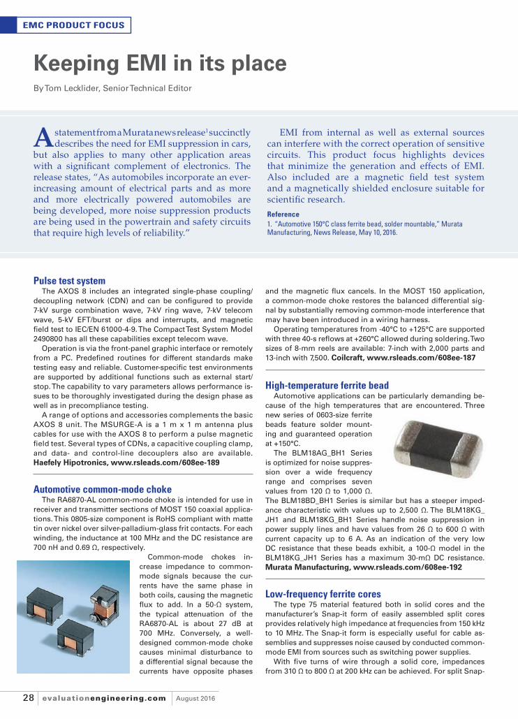
August 2016evaluationengineering.com28
EMC PRODUCT FOCUS
Keeping EMI in its placeBy Tom Lecklider, Senior Technical Editor
A statement from a Murata news release1 succinctly describes the need for EMI suppression in cars,
but also applies to many other application areas with a signifi cant complement of electronics. The release states, “As automobiles incorporate an ever-increasing amount of electrical parts and as more and more electrically powered automobiles are being developed, more noise suppression products are being used in the powertrain and safety circuits that require high levels of reliability.”
Pulse test systemThe AXOS 8 includes an integrated single-phase coupling/
decoupling network (CDN) and can be confi gured to provide
7-kV surge combination wave, 7-kV ring wave, 7-kV telecom
wave, 5-kV EFT/burst or dips and interrupts, and magnetic
fi eld test to IEC/EN 61000-4-9. The Compact Test System Model
2490800 has all these capabilities except telecom wave.
Operation is via the front-panel graphic interface or remotely
from a PC. Predefi ned routines for different standards make
testing easy and reliable. Customer-specifi c test environments
are supported by additional functions such as external start/
stop. The capability to vary parameters allows performance is-
sues to be thoroughly investigated during the design phase as
well as in precompliance testing.
A range of options and accessories complements the basic
AXOS 8 unit. The MSURGE-A is a 1 m x 1 m antenna plus
cables for use with the AXOS 8 to perform a pulse magnetic
fi eld test. Several types of CDNs, a capacitive coupling clamp,
and data- and control-line decouplers also are available.
Haefely Hipotronics, www.rsleads.com/608ee-189
Automotive common-mode chokeThe RA6870-AL common-mode choke is intended for use in
receiver and transmitter sections of MOST 150 coaxial applica-
tions. This 0805-size component is RoHS compliant with matte
tin over nickel over silver-palladium-glass frit contacts. For each
winding, the inductance at 100 MHz and the DC resistance are
700 nH and 0.69 Ω, respectively.
Common-mode chokes in-
crease impedance to common-
mode signals because the cur-
rents have the same phase in
both coils, causing the magnetic
fl ux to add. In a 50-Ω system,
the typical attenuation of the
RA6870-AL is about 27 dB at
700 MHz. Conversely, a well-
designed common-mode choke
causes minimal disturbance to
a differential signal because the
currents have opposite phases
Reference1. “Automotive 150°C class ferrite bead, solder mountable,” Murata Manufacturing, News Release, May 10, 2016.
and the magnetic fl ux cancels. In the MOST 150 application,
a common-mode choke restores the balanced differential sig-
nal by substantially removing common-mode interference that
may have been introduced in a wiring harness.
Operating temperatures from -40°C to +125°C are supported
with three 40-s refl ows at +260°C allowed during soldering. Two
sizes of 8-mm reels are available: 7-inch with 2,000 parts and
13-inch with 7,500. Coilcraft, www.rsleads.com/608ee-187
High-temperature ferrite beadAutomotive applications can be particularly demanding be-
cause of the high temperatures that are encountered. Three
new series of 0603-size ferrite
beads feature solder mount-
ing and guaranteed operation
at +150°C.
The BLM18AG_BH1 Series
is optimized for noise suppres-
sion over a wide frequency
range and comprises seven
values from 120 Ω to 1,000 Ω.
The BLM18BD_BH1 Series is similar but has a steeper imped-
ance characteristic with values up to 2,500 Ω. The BLM18KG_
JH1 and BLM18KG_BH1 Series handle noise suppression in
power supply lines and have values from 26 Ω to 600 Ω with
current capacity up to 6 A. As an indication of the very low
DC resistance that these beads exhibit, a 100-Ω model in the
BLM18KG_JH1 Series has a maximum 30-mΩ DC resistance.
Murata Manufacturing, www.rsleads.com/608ee-192
Low-frequency ferrite coresThe type 75 material featured both in solid cores and the
manufacturer’s Snap-it form of easily assembled split cores
provides relatively high impedance at frequencies from 150 kHz
to 10 MHz. The Snap-it form is especially useful for cable as-
semblies and suppresses noise caused by conducted common-
mode EMI from sources such as switching power supplies.
With fi ve turns of wire through a solid core, impedances
from 310 Ω to 800 Ω at 200 kHz can be achieved. For split Snap-
EMI from internal as well as external sources can interfere with the correct operation of sensitive circuits. This product focus highlights devices that minimize the generation and effects of EMI. Also included are a magnetic fi eld test system and a magnetically shielded enclosure suitable for scientifi c research.
28-29_EE_201608_EMCProducFocus_FINAL_eb.indd 2828-29_EE_201608_EMCProducFocus_FINAL_eb.indd 28 7/7/2016 11:37:00 AM7/7/2016 11:37:00 AM
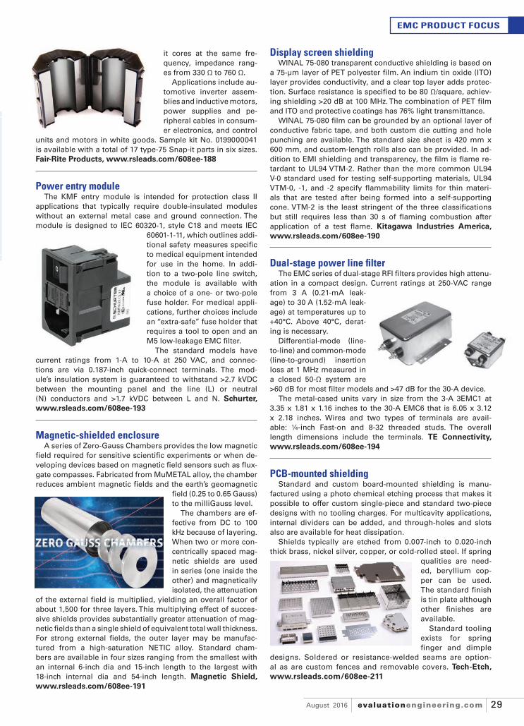
evaluationengineering.comAugust 2016 29
EMC PRODUCT FOCUS
Display screen shieldingWINAL 75-080 transparent conductive shielding is based on
a 75-μm layer of PET polyester fi lm. An indium tin oxide (ITO)
layer provides conductivity, and a clear top layer adds protec-
tion. Surface resistance is specifi ed to be 80 Ω/square, achiev-
ing shielding >20 dB at 100 MHz. The combination of PET fi lm
and ITO and protective coatings has 76% light transmittance.
WINAL 75-080 fi lm can be grounded by an optional layer of
conductive fabric tape, and both custom die cutting and hole
punching are available. The standard size sheet is 420 mm x
600 mm, and custom-length rolls also can be provided. In ad-
dition to EMI shielding and transparency, the fi lm is fl ame re-
tardant to UL94 VTM-2. Rather than the more common UL94
V-0 standard used for testing self-supporting materials, UL94
VTM-0, -1, and -2 specify fl ammability limits for thin materi-
als that are tested after being formed into a self-supporting
cone. VTM-2 is the least stringent of the three classifi cations
but still requires less than 30 s of fl aming combustion after
application of a test fl ame. Kitagawa Industries America, www.rsleads.com/608ee-190
Dual-stage power line fi lterThe EMC series of dual-stage RFI fi lters provides high attenu-
ation in a compact design. Current ratings at 250-VAC range
from 3 A (0.21-mA leak-
age) to 30 A (1.52-mA leak-
age) at temperatures up to
+40°C. Above 40°C, derat-
ing is necessary.
Differential-mode (line-
to-line) and common-mode
(line-to-ground) insertion
loss at 1 MHz measured in
a closed 50-Ω system are
>60 dB for most fi lter models and >47 dB for the 30-A device.
The metal-cased units vary in size from the 3-A 3EMC1 at
3.35 x 1.81 x 1.16 inches to the 30-A EMC6 that is 6.05 x 3.12
x 2.18 inches. Wires and two types of terminals are avail-
able: ¼-inch Fast-on and 8-32 threaded studs. The overall
length dimensions include the terminals. TE Connectivity, www.rsleads.com/608ee-194
PCB-mounted shieldingStandard and custom board-mounted shielding is manu-
factured using a photo chemical etching process that makes it
possible to offer custom single-piece and standard two-piece
designs with no tooling charges. For multicavity applications,
internal dividers can be added, and through-holes and slots
also are available for heat dissipation.
Shields typically are etched from 0.007-inch to 0.020-inch
thick brass, nickel silver, copper, or cold-rolled steel. If spring
qualities are need-
ed, beryllium cop-
per can be used.
The standard fi nish
is tin plate although
other fi nishes are
available.
Standard tooling
exists for spring
fi nger and dimple
designs. Soldered or resistance-welded seams are option-
al as are custom fences and removable covers. Tech-Etch, www.rsleads.com/608ee-211
it cores at the same fre-
quency, impedance rang-
es from 330 Ω to 760 Ω.
Applications include au-
tomotive inverter assem-
blies and inductive motors,
power supplies and pe-
ripheral cables in consum-
er electronics, and control
units and motors in white goods. Sample kit No. 0199000041
is available with a total of 17 type-75 Snap-it parts in six sizes.
Fair-Rite Products, www.rsleads.com/608ee-188
Power entry moduleThe KMF entry module is intended for protection class II
applications that typically require double-insulated modules
without an external metal case and ground connection. The
module is designed to IEC 60320-1, style C18 and meets IEC
60601-1-11, which outlines addi-
tional safety measures specifi c
to medical equipment intended
for use in the home. In addi-
tion to a two-pole line switch,
the module is available with
a choice of a one- or two-pole
fuse holder. For medical appli-
cations, further choices include
an “extra-safe” fuse holder that
requires a tool to open and an
M5 low-leakage EMC fi lter.
The standard models have
current ratings from 1-A to 10-A at 250 VAC, and connec-
tions are via 0.187-inch quick-connect terminals. The mod-
ule’s insulation system is guaranteed to withstand >2.7 kVDC
between the mounting panel and the line (L) or neutral
(N) conductors and >1.7 kVDC between L and N. Schurter, www.rsleads.com/608ee-193
Magnetic-shielded enclosureA series of Zero-Gauss Chambers provides the low magnetic
fi eld required for sensitive scientifi c experiments or when de-
veloping devices based on magnetic fi eld sensors such as fl ux-
gate compasses. Fabricated from MuMETAL alloy, the chamber
reduces ambient magnetic fi elds and the earth’s geomagnetic
fi eld (0.25 to 0.65 Gauss)
to the milliGauss level.
The chambers are ef-
fective from DC to 100
kHz because of layering.
When two or more con-
centrically spaced mag-
netic shields are used
in series (one inside the
other) and magnetically
isolated, the attenuation
of the external fi eld is multiplied, yielding an overall factor of
about 1,500 for three layers. This multiplying effect of succes-
sive shields provides substantially greater attenuation of mag-
netic fi elds than a single shield of equivalent total wall thickness.
For strong external fi elds, the outer layer may be manufac-
tured from a high-saturation NETIC alloy. Standard cham-
bers are available in four sizes ranging from the smallest with
an internal 6-inch dia and 15-inch length to the largest with
18-inch internal dia and 54-inch length. Magnetic Shield, www.rsleads.com/608ee-191
28-29_EE_201608_EMCProducFocus_FINAL_eb.indd 2928-29_EE_201608_EMCProducFocus_FINAL_eb.indd 29 7/21/2016 3:05:12 PM7/21/2016 3:05:12 PM
August 2016evaluationengineering.com30
DC/DC converterThe NXE2 Series 2-W sur-
face-mounted DC/DC convert-
ers are footprint-compatible
with similar 1-W and 2-W de-
vices available on the market
and measure just 12.5 x 4.36 x
10.41 mm. The converter is con-
structed using fully automated
techniques in a halogen-free
iLGA inspectable package with an integrated transformer. This
approach increases product reliability and repeatability of con-
verter performance.
The series comprises four models with nominal input volt-
ages of +5 or +12 VDC and outputs of +5, +12, or +15 VDC.
Input-to-output isolation of 3 kVDC is standard across the
range. The NXE2 series is suitable for use in industrial auto-
mation, instrumentation, and transportation equipment. It
also is intended for use in telecom, wireless, and medical de-
signs that require a low-power isolated DC voltage. Murata, www.rsleads.com/608ee-195
Functional test platformThe GENASYS functional test platform now includes two
new products. Building on the architecture of the GENASYS
switching subsystem, the vendor has added the GX7017 inte-
grated GENASYS chassis to the GENASYS product line, provid-
ing digital, analog, and high-performance switching capability
within a single, compact, 6U PXI chassis footprint. The GX7017
is a 20-slot 6U PXI chassis with an integrated MAC Panel SCOUT
mass interconnect receiver that can accommodate up to nine
GENASYS switching modules, eight high-performance digital
instruments, and additional PXI instrument modules.
To further extend the switching capabilities of the GENA-
SYS platform, the vendor has introduced the GX6864, a 500-
MHz, 75-Ω RF multiplexer switch module for high I/O count,
video switching/test applications. Marvin Test Solutions, www.rsleads.com/608ee-196
FFT optionAn improved FFT op-
tion now is available
for the U5303A PCIe
12-bit high-speed data
acquisition card. This
card features two chan-
nels and a sampling
rate from 1 GS/s to 3.2
GS/s. Designed for astronomy, physics applications, and envi-
ronmental measurements requiring frequency-domain signal
processing, the card allows observation of phenomena never
observed before with previous instruments, offering a step for-
ward in terms of linearity, dynamic range, and spurious free
dynamic range measurements.
While providing continuous real-time FFT at full sampling
rate, this option also enables spectra accumulation capabil-
ity, a key requirement for radio astronomy. This application
option comes with a dedicated FFT spectrometer graphic
user interface to facilitate fast initial startup, display, and
export of the acquired FFT data. Keysight Technologies, www.rsleads.com/608ee-197
Debug fi rmware upgradeA J-Link fi rmware upgrade supports the embedded ST-LINK
on STM32 Nucleo, STM32 Discovery, and other microcontroller
unit evaluation boards from STMicroelectronics. The upgrade
turns a board’s ST-LINK interface
into a fully functional J-Link,
which then can be employed to
debug the board’s application
processor. By upgrading to the
J-Link fi rmware, developers sub-
sequently will be able to set an
unlimited number of breakpoints
in fl ash memory and debug their
applications considerably faster,
resulting in better use of engineering resources and shortened
time to market. SEGGER, www.rsleads.com/608ee-198
TEDS force sensorsHBM’s growing line of force
sensors is available with a
Transducer Electronic Data
Sheet (TEDS) memory mod-
ule designed to store sensor
properties, thereby simplify-
ing the process of confi guring a force measurement system.
A TEDS module speeds the system confi guration process
by having the individual characteristics of the force sensor, in-
cluding sensitivity, nominal (rated) force, supply voltage, serial
number, and transducer type saved to memory when the sen-
sor is delivered. The amplifi er system reads the chip automati-
cally and confi gures the measurement module with the correct
sensor data. HBM, www.rsleads.com/608ee-199
60-GHz development systemThe PEM009-KIT 60-GHz development system offers design-
ers the ability to perform product development and experi-
mentation of single and multicarrier high-bandwidth modula-
tion covering 57 GHz to 64 GHz in the globally unlicensed ISM
frequency spectrum.
The development system
supports a variety of I/Q (vec-
tor) and FSK/MSK modulation
schemes from a user-designed
baseband system or a vector-
modulated programmable ar-
bitrary waveform generator.
The system is confi gured as a
standalone benchtop wireless
link where transmitted power
directly from the waveguide aperture is equivalent to a 7-dBi
gain horn antenna with a 70-degree wide beam pattern that’s
useful to test and demonstrate various modulation schemes
and data rates. Pasternack, www.rsleads.com/608ee-200
High-voltage reed relaysSeries 67 and 68 reed relays are available for up to 10-kV
stand-off, 7.5-kV switching, with an option of either PCB or
fl ying-lead switch connections. Similar in specifi cation to the
vendor’s Series 60/65, these new relays are manufactured in a
single-in-line format using former-less coils, which dispenses
EE PRODUCT PICKS
30-31_EE_201608_ProductPicks_FINAL_eb.indd 3030-31_EE_201608_ProductPicks_FINAL_eb.indd 30 7/7/2016 3:14:12 PM7/7/2016 3:14:12 PM
evaluationengineering.comAugust 2016 31
EE PRODUCT PICKS EE LITERATUREMARKETPLACE
with the more usual coil supporting
bobbin, allowing a smaller package
than similar rated devices.
The package design presents some
interesting possibilities for high-density
applications such as multiplexers and
matrices in instrumentation and test sys-
tems; Series 67 relays mounted on a 3U
PXI 12-way high-voltage multiplexer module illustrates these pos-
sibilities. Pickering Electronics, www.rsleads.com/608ee-201
USB hubThe USB-104-IHUB medical/in-
dustrial/military-grade USB hub fea-
tures the company’s Tru-Iso signal
isolation up to 4 kV, extended tem-
perature operation (-40°C to 85°C),
high-retention USB connectors,
and an industrial steel enclosure for
shock and vibration mitigation.
The USB-104-IHUB makes it easy to expand the number of
USB ports and provide up to 4-kV isolation between the host
computer and connected USB peripherals. Applications in-
clude factory automation, hospital and medical, energy man-
agement, military/mission-critical, transportation, security
systems, and process monitoring. $295. ACCES I/O Products, www.rsleads.com/608ee-202
Spectrum monitoring moduleThe MS27100A spectrum monitoring module brings the ven-
dor’s RF spectrum-analysis technology to OEM applications. Engi-
neers designing systems to locate illegal and unlicensed interfer-
ing signals within wireless networks can integrate the MS27100A
into custom hardware to achieve
a cost-effi cient, accurate tool pri-
marily for security, aerospace, and
defense applications.
Covering the 9-kHz to 6-GHz
frequency range, the MS27100A
is capable of sweeping at rates
up to 24 GHz/s, allowing many
types of signals, including periodic or transient transmissions
as well as short “bursty” signals, to be captured. Anritsu, www.rsleads.com/608ee-203
High-density receptaclesFour off-the-shelf receptacles
are suitable for use in high-densi-
ty confi gurations down to 1-mm
pitch. Each receptacle contains
the company’s three-fi nger be-
ryllium copper contact with a di-
ameter range of 0.008 inch (0.2 mm) to 0.013 inch (0.33 mm).
The contact is characterized by a low insertion force, making it
compatible with miniature leads subject to bending.
Two of the receptacles, 0439-0-15-15-04-27-04-0 and 8210-
0-15-15-04-27-04-0, have solder tails for through-hole appli-
cations. The 4428-0-43-15-04-14-10-0 is a low-profi le, solder-
mount, open-bottom model. The 9928-0-15-15-04-27-40-0 is a
SMT receptacle mainly used for 1-mm grid socket confi gura-
tions. Mill-Max, www.rsleads.com/608ee-204
NEW AR COMPREHENSIVE PRODUCT CATALOG!
Many exciting new products includ-
ing high power solid state pulsed
amplifi ers and new USB peak power
sensors are featured. Read about our
new RF solid state water cooled am-
plifi ers with respective chillers, see
photos of the expanded microelec-
tronics lab, and learn about AR Eu-
rope’s new partnership with CETC41.
AR RF/MicrowaveVisit www.rsleads.com/608ee-362
PRODUCT SAFETY TEST EQUIPMENT
ED&D, a world leader in Prod-
uct Safety Test Equipment man-
ufacturing, offers a full line of
equipment for meeting various
UL, IEC, CSA, CE, ASTM, MIL,
and other standards. Product
line covers categories such as
hipot, leakage current, ground,
force, impact, burn, tempera-
ture, access, ingress (IP code),
cord fl ex, voltage, power, plas-
tics, and others. ED&D
Visit www.rsleads.com/608ee-360
IP CODE & NEMA TESTINGCertifi Group offers a full UL, CSA, IEC and
CE, ISO 17025 Accredited International
Product Test & Certifi cation Laboratory.
The lab includes a unique indoor wet-
lab, where Certifi Group specializes in
IP Code & NEMA testing for products
subject to dust, water ingress and similar
hazards. The Certifi Group indoor IP Code
Wet Lab is one of the world’s largest and
most cutting-edge.IP Code capabilities
up to IP69K! Certifi Group
Visit www.rsleads.com/608ee-361
Inde
x of
Adv
erti
sers ADVERTISER PAGE
This index is provided as a service. The publisher does not assume liability for
errors or omissions.
AR RF/Microwave ..................................www.arworld.us ............................................... 5AR RF/Microwave ..................................http://www.arworld.us/html/catalogRequest .. 31Certifi Group .............................................www.Certifi Group.com .................................. 31Educated Design & Development. Inc. ..www.ProductSafet.com ................................ 31Keysight Technologies .........................www.keysight.com/fi nd/ScopeMVP .......... 11Keysight Technologies .........................www.keysight.com/fi nd/AmericasOneSource .. 17Marvin Test Solutions ...........................www.marvintest.com/ateasy25 ..................BCMeasurement Computing Corp ...........mccdaq.com/ethernet ...................................... 9National Instruments ............................ni.com/smarter-test ....................................... IFCPickering Interfaces Inc. ......................www.pickeringtest.com/advantage ............. 3Pico Technology .....................................www.picotech.com ........................................ 13Virginia Panel Corp. ..............................www.vpc.com/EE2 .......................................... 19
30-31_EE_201608_ProductPicks_FINAL_eb.indd 3130-31_EE_201608_ProductPicks_FINAL_eb.indd 31 7/8/2016 9:37:41 AM7/8/2016 9:37:41 AM

August 2016evaluationengineering.com32
RESEARCH INSIGHTS
By Rick Nelson, Executive Editor
GaN shows promise for transportation, communications applications
Gallium nitride is a promising semiconductor process for pow-er-electronics devices serving ap-
plications ranging from transportation to communications infrastructure. Research into GaN technology, which compared with silicon offers higher breakdown voltages, faster speeds, and lower on-resistance, is proceeding as companies bring practical GaN devices to market.
On the research front, imec, the nano-electronics research center, announced in May a strategic partnership regarding gallium nitride-on-silicon (GaN-on-Si) technology with IQE, which provides advanced semiconductor wafer products and services. The partnership builds on promising results achieved in a recent project in which imec and IQE collabo-rated to fabricate GaN power diodes us-ing imec’s proprietary diode architecture and IQE’s high-voltage epiwafers.
In that project, imec applied its Gated Edge Terminated (GET) Schottky diode device architecture to IQE’s high-voltage GaN buffers on 200-mm Si substrates. Thanks to the GET diode device archi-tecture and the low buffer leakage cur-rent of IQE wafers, the large GaN power diodes (10 mm) that were fabricated in imec’s 200-mm Si pilot line showed a low leakage current (at up to 650 V) and low turn-on voltage. The power Schottky di-odes reach forward and reverse specifi -cations across the full temperature range, spanning from 25°C to 150°C with a tight distribution (see fi gure). The diodes have 10-mm anode width and an anode-to-cathode distance of 10 μm.
IQE will be participating in imec’s GaN-on-Si Industrial Affi liation Pro-
gram, which offers joint research and development on GaN-on-Si 200-mm epitaxy and enhancement-mode device technology to a variety of companies including IDMs, equipment and mate-rial suppliers, fabless design houses, and packaging companies. The program includes research on novel substrates to improve the quality of epitaxial layers, new isolation modules to enhance inte-gration levels, and advanced vertical de-vice development.
Wayne Johnson, head of IQE’s Power Business Unit, said in a press release, “The importance of GaN-on-Si for power devices cannot be understated, particu-larly as we enter an era of electrically propelled transportation and increasing demands for energy-effi cient power control systems that require high-volt-age and high-power capabilities.” Rudi Cartuyvels, executive vice president for smart systems and energy technology at imec, added that the organization’s 200-mm GaN-on-Si process can be engineered to fi t partner-specifi c product needs.
In related news, IQE announced in May that it has successfully transferred Translucent cREO (for Rare Earth Ox-ide) semiconductor technology to IQE’s facility in Greensboro, NC (IQE an-nounced an exclusive license of cREO technology from Translucent parent company Silex Systems in September 2015), where a production tool now is producing cREO templates on Si. IQE said GaN-on-Si typically exhibits an undesirable p-type parasitic channel at the GaN/Si interface that detrimentally affects RF effi ciency. But using patented technology, IQE said it has demonstrat-
ed that the parasitic channel can be com-pletely eliminated.
Dr. Rodney Pelzel, vice president, IQE Group Technology, com-mented in a press re-lease, “We have demon-strated that we are able to rationally manipulate the cREO characteristics to tune the conductivity of the III-N/Si interface. This is a signifi cant en-abler for GaN HEMT technology on Si for RF applications. In addi-tion, it is an enabler for
other III-N technology on Si such as RF fi lter technology.”
The International Microwave Sympo-sium in May provided a venue for com-panies to tout the GaN devices they are making for commercial and military ap-plications. NXP, for example, launched an expansion to its portfolio of 48-V GaN RF power transistors optimized for Doherty power amplifi ers for use in current and next-generation cellular base stations, according to Jim Norling, vice president, cellular infrastructure. He added that NXP also has expanded its portfolio of broadband GaN RF power transistors for electronic warfare and bat-tlefi eld radio applications.
Qorvo announced, in conjunction with NanoSemi, a developer of digital linear-ization and compensation algorithms, that it has demonstrated industry-lead-ing ultra-wideband linearization results with its GaN power amplifi ers for wire-less infrastructure. The demonstration employed Qorvo’s QPA2705 integrated GaN driver and GaN Doherty power amplifi er along with NanoSemi’s propri-etary digital compensation algorithms.
Sumit Tomar, general manager of Qorvo’s Wireless Infrastructure busi-ness unit, said Qorvo’s compact PAs and NanoSemi’s digital-predistortion IP will help customers meet challenges that appear when implementing next-generation base stations such as those having active antenna systems with 64 transceivers—which require small form factors, high effi ciency, and linearity to support multicarrier confi gurations.
Wolfspeed offered live product dem-onstrations at IMS. One centered on the CGHV14800, a high-power GaN HEMT device designed for L-Band ra-dar applications. Another employed the CGHV59070 GaN HEMT for C-band ra-dar systems. Yet a third demonstration showcased a wideband LTE Doherty power amplifi er developed using the company’s high-performance 0.4-μm 50-V GaN RF foundry process.
Ryan Baker, product marketing man-ager for RF components, cited a mile-stone the company has reached. As of the end of 2015, he said, Wolfspeed had shipped GaN-on-SiC RF power transis-tors with a combined RF output power of more than 1.3 GW (suffi cient to pow-er 124,900 U.S. residential homes for a year). EEForward and reverse diode current at high temperature (150°C)
Courtesy of imec
32-BC_EE_201608_ResearchInsight_FINAL_eb.indd 3232-BC_EE_201608_ResearchInsight_FINAL_eb.indd 32 7/7/2016 11:54:04 AM7/7/2016 11:54:04 AM

32-BC_EE_201608_ResearchInsight_FINAL_eb.indd CoverIII32-BC_EE_201608_ResearchInsight_FINAL_eb.indd CoverIII 7/7/2016 11:54:36 AM7/7/2016 11:54:36 AM

Simplify logistics and save deployment space with innovative,
ultra-rugged, aerospace-quality modular solutions
© 2016 Marvin Test Solutions, Inc. All rights reserved. Product and trade names are property of their respective companies.
Transform Your Test CapabilitiesFrom the Flightline to the Factory
MARVINTEST.COM
Flexibility, Performance, & Unrivaled Long-Term Support
Join us at AUTOTESTCON 2016Booth #813
Reduced Footprint
Automation
Update and optimize your legacy systems and next-
generation test needs with PXI-based test platforms
ATEasy 1.0 was released in in 1991. Nine
generations and 25 years later, ATEasy
continues to make automated test easy, offering
comprehensive simulation, an integrated test
executive / test development software suite, and
unrivaled long term product support.
Learn more at www.marvintest.com/ateasy25
S
u
R
Visit www.rsleads.com/608ee-002
32-BC_EE_201608_ResearchInsight_FINAL_eb.indd CoverIV32-BC_EE_201608_ResearchInsight_FINAL_eb.indd CoverIV 7/7/2016 11:55:12 AM7/7/2016 11:55:12 AM