Embed Size (px)
Citation preview
FD
R o
f the
End
-cap
Muo
n T
rigg
er E
lect
roni
cs 1
/Mar
./04
1
SLB ASIC
IntroductionStructure
Input & JTAG block Trigger block Readout block
Prototype Development HistoryVersion 4 submission status
Chikara Fukunaga (TMU)
FD
R o
f the
End
-cap
Muo
n T
rigg
er E
lect
roni
cs 1
/Mar
./04
2
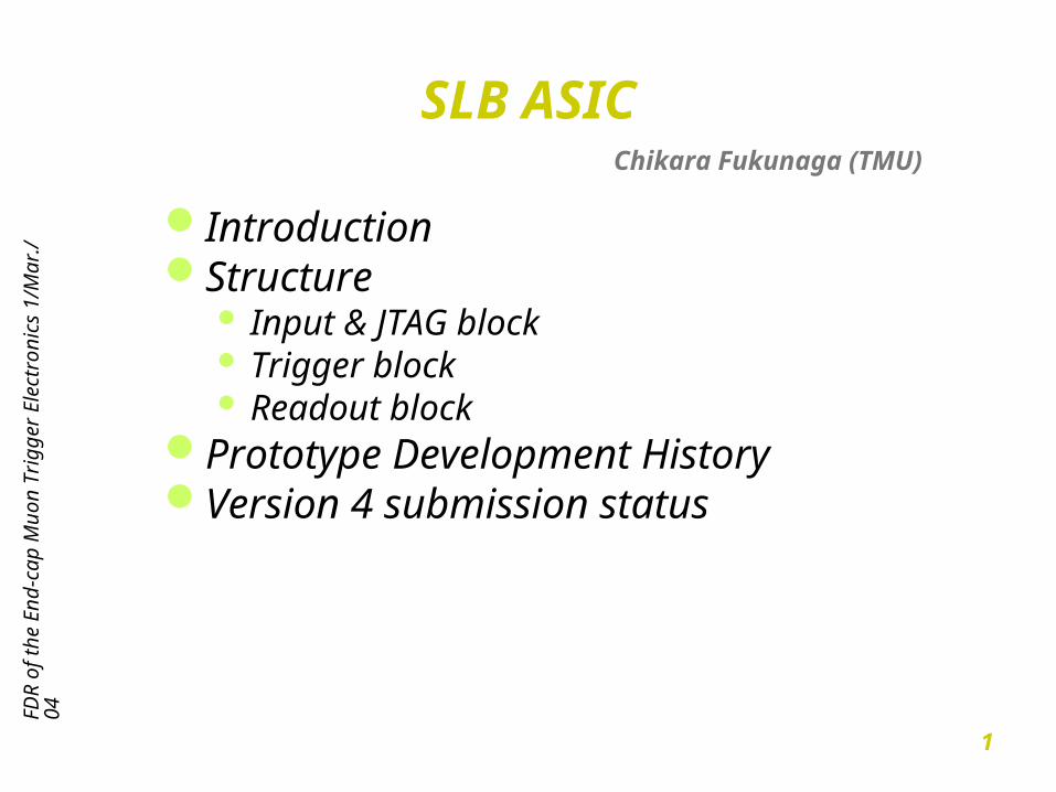
Introduction
ASIC Layout Mask Pattern ROHM 0.35m Gate Width CMOS
processed in 9.72x9.72mm2 die 200Kgates Four blocks are clearly
seen in figure due tomacro-core place and route
Input
JTAG
Readout Trigger
FD
R o
f the
End
-cap
Muo
n T
rigg
er E
lect
roni
cs 1
/Mar
./04
3
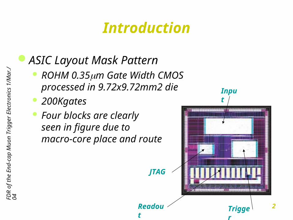
Structure
20bit (+20bit)
x 4From TTC
clk,BCR,ECR,L1A
Blocks:
1. Trigger
2. Readout
3. JTAG
4. Input
FD
R o
f the
End
-cap
Muo
n T
rigg
er E
lect
roni
cs 1
/Mar
./04
4
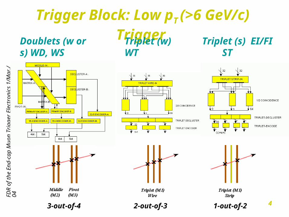
Trigger Block: Low pT (>6 GeV/c) Trigger Doublets (w or s) WD, WS
Triplet (w) WT
Triplet (s) EI/FI ST
3-out-of-4 2-out-of-3 1-out-of-2
FD
R o
f the
End
-cap
Muo
n T
rigg
er E
lect
roni
cs 1
/Mar
./04
5
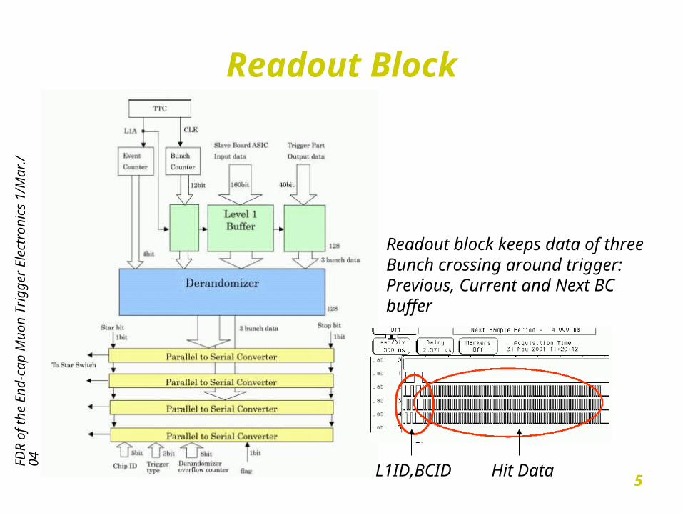
Readout Block
Readout block keeps data of three Bunch crossing around trigger: Previous, Current and Next BC buffer
L1ID,BCID Hit Data
FD
R o
f the
End
-cap
Muo
n T
rigg
er E
lect
roni
cs 1
/Mar
./04
6
Input Block & JTAG Block
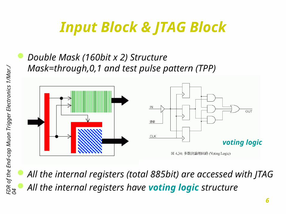
Double Mask (160bit x 2) StructureMask=through,0,1 and test pulse pattern (TPP)
All the internal registers (total 885bit) are accessed with JTAGAll the internal registers have voting logic structure
voting logic
FD
R o
f the
End
-cap
Muo
n T
rigg
er E
lect
roni
cs 1
/Mar
./04
7
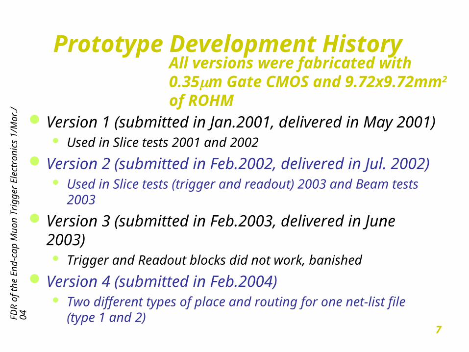
Prototype Development History
Version 1 (submitted in Jan.2001, delivered in May 2001) Used in Slice tests 2001 and 2002
Version 2 (submitted in Feb.2002, delivered in Jul. 2002) Used in Slice tests (trigger and readout) 2003 and Beam tests 2003
Version 3 (submitted in Feb.2003, delivered in June 2003) Trigger and Readout blocks did not work, banished
Version 4 (submitted in Feb.2004) Two different types of place and routing for one net-list file (type 1
and 2)
All versions were fabricated with 0.35m Gate CMOS and 9.72x9.72mm2 of ROHM
FD
R o
f the
End
-cap
Muo
n T
rigg
er E
lect
roni
cs 1
/Mar
./04
8
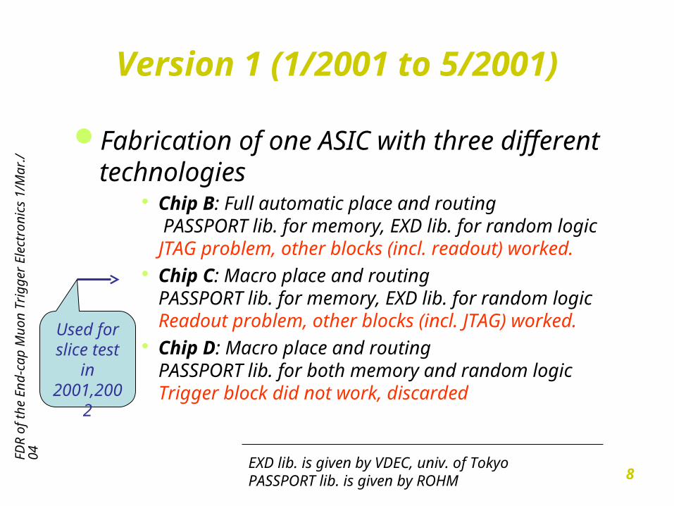
Version 1 (1/2001 to 5/2001)
Fabrication of one ASIC with three different technologies
Chip B: Full automatic place and routing PASSPORT lib. for memory, EXD lib. for random logicJTAG problem, other blocks (incl. readout) worked.
Chip C: Macro place and routing PASSPORT lib. for memory, EXD lib. for random logicReadout problem, other blocks (incl. JTAG) worked.
Chip D: Macro place and routingPASSPORT lib. for both memory and random logicTrigger block did not work, discarded
Used for slice test
in 2001,2002
EXD lib. is given by VDEC, univ. of TokyoPASSPORT lib. is given by ROHM
FD
R o
f the
End
-cap
Muo
n T
rigg
er E
lect
roni
cs 1
/Mar
./04
9
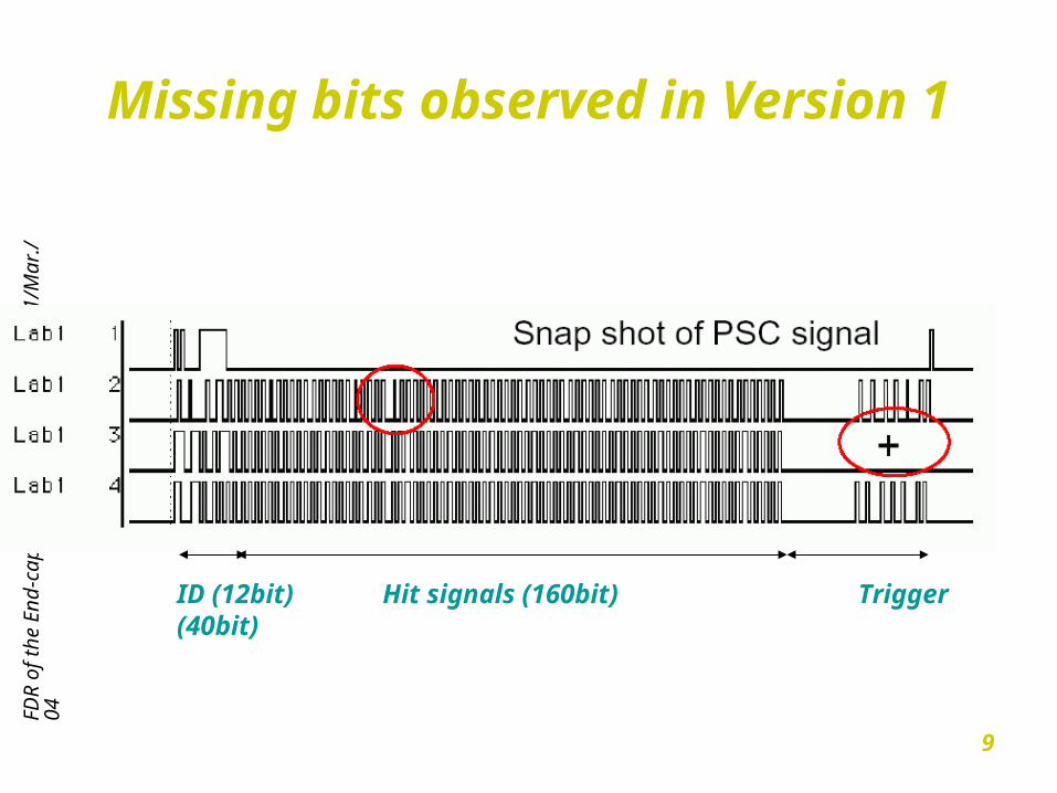
Missing bits observed in Version 1
ID (12bit) Hit signals (160bit) Trigger (40bit)
FD
R o
f the
End
-cap
Muo
n T
rigg
er E
lect
roni
cs 1
/Mar
./04
10
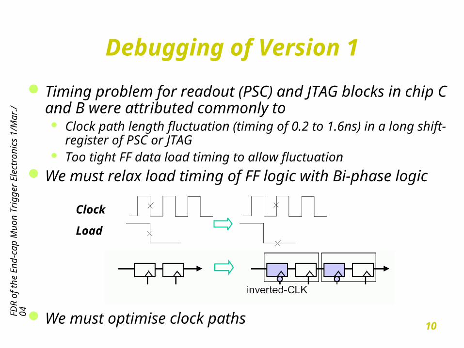
Debugging of Version 1
Timing problem for readout (PSC) and JTAG blocks in chip C and B were attributed commonly to Clock path length fluctuation (timing of 0.2 to 1.6ns) in a long shift-regis
ter of PSC or JTAG Too tight FF data load timing to allow fluctuation
We must relax load timing of FF logic with Bi-phase logic
We must optimise clock paths
Clock
Load
FD
R o
f the
End
-cap
Muo
n T
rigg
er E
lect
roni
cs 1
/Mar
./04
11
Version 2 (2/2002 to 7/2002)
Prescriptions found in debugging of version 1 were involved, Bi-phase logic for Shift reg. FF data load, and Manual place and routing for clock distribution path.
Standard JTAG (so-called dialect was corrected)JTAG access for all the user registersand so forth (minor things)After version 1 to version 4 now, we keep
PASSPORT lib. for memory cells, and EXD lib. for random logic cells.
FD
R o
f the
End
-cap
Muo
n T
rigg
er E
lect
roni
cs 1
/Mar
./04
12
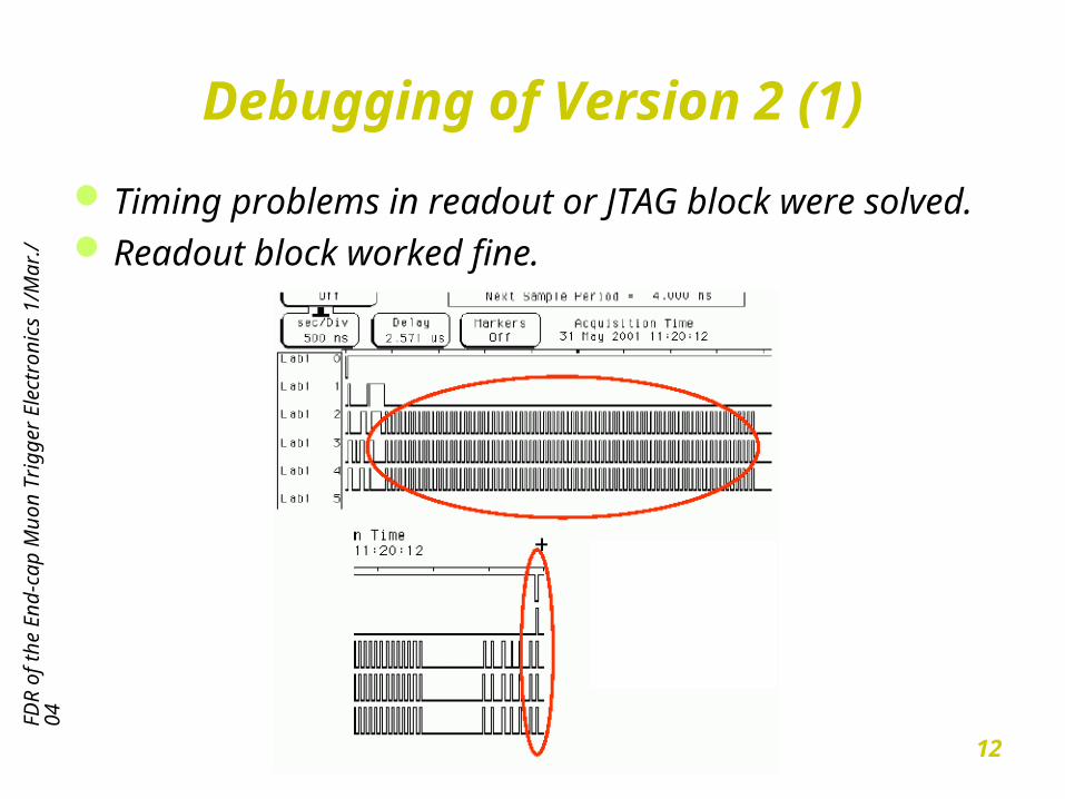
Debugging of Version 2 (1)
Timing problems in readout or JTAG block were solved. Readout block worked fine.

FD
R o
f the
End
-cap
Muo
n T
rigg
er E
lect
roni
cs 1
/Mar
./04
13
Debugging of Version 2 (2)
20 pins of total 40bit output for ST trigger are used as adjacent input pins for WD or WT trigger. ENB signal lines to switch input/output for these 20 pins were found not to be connected at all.
Pins were valid only for output. Adjacent signals for WD and WT could not be inputted.
So far we made debug with test vectors, which did not require adjacent inputs.
FD
R o
f the
End
-cap
Muo
n T
rigg
er E
lect
roni
cs 1
/Mar
./04
14
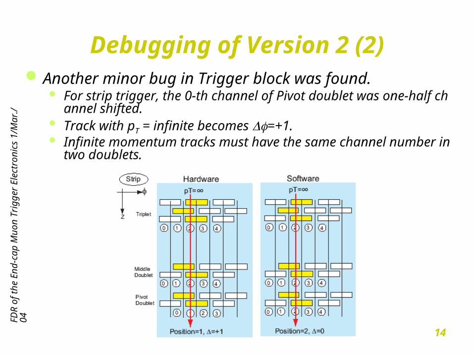
Debugging of Version 2 (2)Another minor bug in Trigger block was found.
For strip trigger, the 0-th channel of Pivot doublet was one-half channel shifted.
Track with pT = infinite becomes =+1. Infinite momentum tracks must have the same channel number in two do
ublets.
FD
R o
f the
End
-cap
Muo
n T
rigg
er E
lect
roni
cs 1
/Mar
./04
15
Version 3 (2/2003 to 6/2003)
Fix of I/O pad problem Correction of=0 for infinite momentum track Increase of input delay adjust range (2 3bit) 0 to 3.5clocks Individual input delay adjustment for four input groups
(so far all inputs used the same delay) Modification of Readout output sequence
trigger bits (40bits) before hit signals (160bit) Removal of Boundary scan registers for i/o pins (simplification)
But neither trigger nor readout block worked correctly. The chip has been discarded quickly even full debug were not
finished.
FD
R o
f the
End
-cap
Muo
n T
rigg
er E
lect
roni
cs 1
/Mar
./04
16
Version 4 (submitted in Feb.,2004)
Starting from Version 2 with minimum modification to fix known bugs (we have begun to design since October,2003), Fix of I/O pad problem Correction of=0 for infinite momentum track Increase of input delay adjust range (2 3bit) of 0 to 3.5clocks and a
ddition of another positive FF (new delay range of 1 to 4.5 clocks) Individual input delay adjustment for four input groups (so far all input
s used the same delay)Two independent place and routings (type 1 and type 2) by two
different chip designers (R.Ichimiya and H.Kano) from the single net-list file Type-1 is more optimisation to clock tree than allocation of macro cells Type-2 is more optimisation to allocation of macro cells than clock tree
FD
R o
f the
End
-cap
Muo
n T
rigg
er E
lect
roni
cs 1
/Mar
./04
17
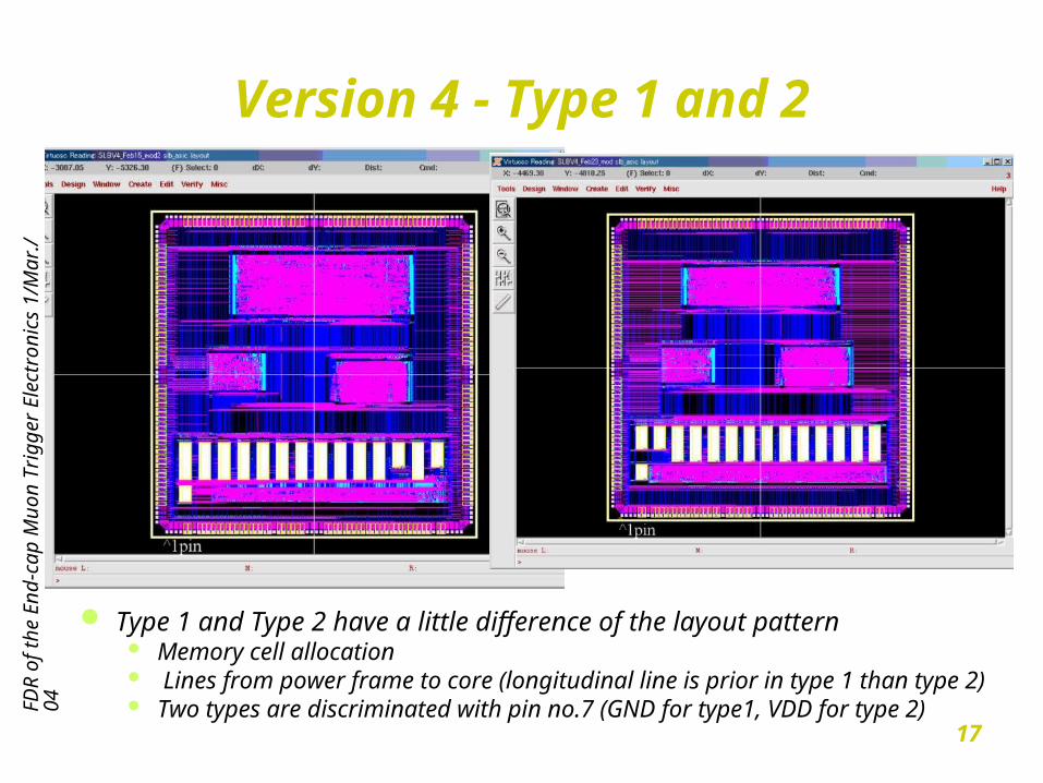
Version 4 - Type 1 and 2
Type 1 and Type 2 have a little difference of the layout pattern Memory cell allocation Lines from power frame to core (longitudinal line is prior in type 1 than type 2) Two types are discriminated with pin no.7 (GND for type1, VDD for type 2)
FD
R o
f the
End
-cap
Muo
n T
rigg
er E
lect
roni
cs 1
/Mar
./04
18
Version 4 schedule
Chip will be delivered in June 2004.We intend, and hope
Debug will be completed in a month,Check will be (must be) passed successfullyWe will then order for production in summer


![[1] Schmitt Trigger: A building block in which the input must be taken](https://img.pdfslide.net/doc/110x75/5891a07f1a28ab05408bbacd/1-schmitt-trigger-a-building-block-in-which-the-input-must-be-taken-.jpg)