Embed Size (px)
Citation preview

DATA SHEET
IDT8V44N003NLGI REVISION A APRIL 24, 2012 1 ©2012 Integrated Device Technology, Inc.
FemtoClock® NG LVDS Clock Synthesizer IDT8V44N003I
General Description
The IDT8V44N003I is a programmable LVDS synthesizer designed for applications requiring frequency conversion from a differential or single-end reference source. The device is designed to provide opti-mum performance of low phase noise and high power supply noise rejection over a wide range of output frequencies. Oscillator level phase noise performance is achieved through the use of IDT’s Fourth Generation FemtoClock®NG PLL technology. Default output frequency settings are factory programmable via a one time pro-grammable ROM while the I2C interface can be used to program the output frequency after power up. A buffered copy of the input refer-ence clock is provided at both LVDS output levels for applications requiring efficient board space utilization.
Features
• Fourth generation FemtoClock® (NG) technology
• Reference clock input accepts differential HCSL, LVDS, LVPECLor single-ended sine wave or LVCMOS input levels
• Input frequency range of 20MHz to 500MHz
• Output frequency range of 50MHz to 1.2GHz
• Buffered copy of input reference clock at LVDS output levels
• PLL lock indicator
• Full 3.3V output supply mode
• -40°C to 85°C ambient operating temperature
• Available in lead-free (RoHS 6) package
Pin Assignment
VDDA
nc
VDD
nc
SDATA
GND
nc
SCLK
nc
Res
erve
d
VPP nc nc
GN
D nc
GN
D
nc VD
D
nc Q nQ nc GN
D
ncREF_CLKOUT
nREF_CLKOUT
LOCK
REF_CLKIN
nREF_CLKIN
nc
GND
nc1 2 3 4 5 6 7 8
24 23 22 21 20 19 18 17
25
26
27
28
29
30
31
32
16
15
14
13
12
11
10
9
IDT8V44N003I
32 Lead VFQFN5mm x 5mm x 0.925mm Package Body
NL PackageTop View

IDT8V44N003NLGI REVISION A APRIL 24, 2012 2 ©2012 Integrated Device Technology, Inc.
IDT8V44N003I Data Sheet FEMTOCLOCK® NG LVDS CLOCK SYNTHESIZER
Block Diagram
125 73
Pulldown
PU/PD
Pullup
Pullup
LOCK
REF_CLKOUT
nREF_CLKOUT
Q
nQREF_CLKIN
nREF_CLKINPFD&
LPF
÷N
÷ MINT, MFRAC
÷P FemtoClock®NGVCO
1980 - 2550MHz
I2C ControlSCLK
SDATA
0
1
2
VPP

IDT8V44N003NLGI REVISION A APRIL 24, 2012 3 ©2012 Integrated Device Technology, Inc.
IDT8V44N003I Data Sheet FEMTOCLOCK® NG LVDS CLOCK SYNTHESIZER
Table 1. Pin Descriptions
NOTE: Pullup and Pulldown refer to internal input resistors. See Table 2, Pin Characteristics, for typical values.
Table 2. Pin Characteristics
Number Name Type Description
1, 4, 5, 7, 9, 11, 17, 19, 22, 24, 26,
28, 31
nc Unused These pins are to be left unconnected.
2 Reserved Reserve Reserved pin. This pin is left unconnected.
3 VPP Input Pullup Must be connected to ground for proper operation.
6, 8, 10,18, 30
GND Power Power supply ground.
12 nREF_CLKIN InputPullup/
PulldownInverting differential PLL reference clock input.
13 REF_CLKIN Input Pulldown Non-inverting differential PLL reference clock input.
14 LOCK Output PLL lock indicator. LVCMOS/LVTTL interface levels.
15, 16nREF_CLKOUT, REF_CLKOUT
Output Differential output pair. Buffered copy of REF_CLKIN. LVDS interface levels.
20, 21 nQ, Q Output Differential output pair. LVDS interface levels.
23, 27 VDD Power Power supply pins.
25 VDDA Power Analog power supply pin.
29 SDATAInput/Output
PullupI2C data input. Input: LVCMOS/LVTTL interface levels. Output: Open Drain.
32 SCLK Input Pullup I2C clock input. LVCMOS/LVTTL interface levels.
Symbol Parameter Test Conditions Minimum Typical Maximum Units
CIN Input Capacitance 3.5 pF
RPULLUP Input Pullup Resistor 51 kΩ
RPULLDOWN Input Pulldown Resistor 51 kΩ

IDT8V44N003NLGI REVISION A APRIL 24, 2012 4 ©2012 Integrated Device Technology, Inc.
IDT8V44N003I Data Sheet FEMTOCLOCK® NG LVDS CLOCK SYNTHESIZER
Block Diagram with Programming Registers
Pullup
Pullup 35
187
73
Pulldown
PU/PD PFD&
LPF
÷N÷P FemtoClock®NG
VCO1950-2550MHz
MINT(7bits)
MFRAC(18 bits)
Feedback Divider M (25 Bits)
P0 MINT0 MFRAC0 N0
P3 MINT3 MFRAC3 N3
P2 MINT2 MFRAC2 N2
P1 MINT1 MFRAC1 N1
I2C: 3 bits 7 bits 18 bits 7 bits
Def: 3 bits 7 bits 18 bits 7 bits
I2C: 3 bits 7 bits 18 bits 7 bits
Def: 3 bits 7 bits 18 bits 7 bits
7 bits
I2C: 3 bits 7 bits 18 bits 7 bits
Def: 3 bits 7 bits 18 bits 7 bits
I2C: 3 bits 7 bits 18 bits 7 bits
Def: 3 bits 7 bits 18 bits
7 bits
I2C: 3 bits 7 bits 18 bits 7 bits
Def: 3 bits 7 bits 18 bits 7 bits
I2C: 3 bits 7 bits 18 bits 7 bits
Def: 3 bits 7 bits 18 bits
7 bits
I2C: 3 bits 7 bits 18 bits 7 bits
Def: 3 bits 7 bits 18 bits 7 bits
I2C: 3 bits 7 bits 18 bits 7 bits
Def: 3 bits 7 bits 18 bits
35
35
35
35
35
35
35
35
REF_CLKIN
nREF_CLKIN
SCLK
SDATA
LOCK
REF_CLKOUT
nREF_CLKOUT
Q
nQ
00
01
10
11
0
1
I2C Control
1980-2550MHz
VPP
IDT8V44N003NLGI REVISION A APRIL 24, 2012 5 ©2012 Integrated Device Technology, Inc.
IDT8V44N003I Data Sheet FEMTOCLOCK® NG LVDS CLOCK SYNTHESIZER
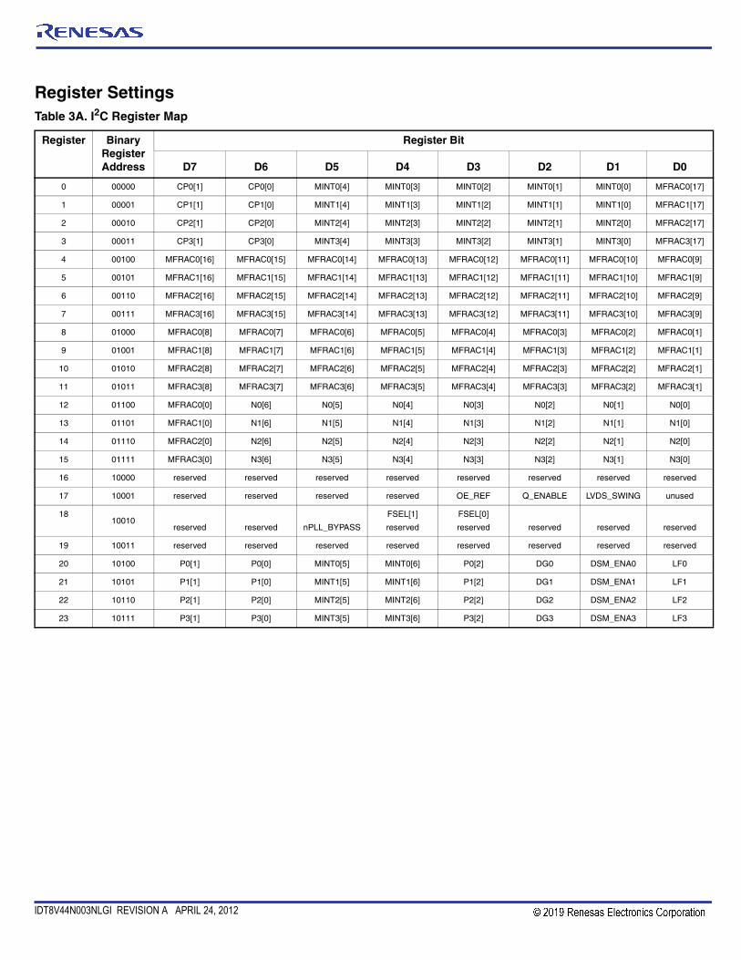
Register SettingsTable 3A. I2C Register Map
Register Binary Register Address
Register Bit
D7 D6 D5 D4 D3 D2 D1 D0
0 00000 CP0[1] CP0[0] MINT0[4] MINT0[3] MINT0[2] MINT0[1] MINT0[0] MFRAC0[17]
1 00001 CP1[1] CP1[0] MINT1[4] MINT1[3] MINT1[2] MINT1[1] MINT1[0] MFRAC1[17]
2 00010 CP2[1] CP2[0] MINT2[4] MINT2[3] MINT2[2] MINT2[1] MINT2[0] MFRAC2[17]
3 00011 CP3[1] CP3[0] MINT3[4] MINT3[3] MINT3[2] MINT3[1] MINT3[0] MFRAC3[17]
4 00100 MFRAC0[16] MFRAC0[15] MFRAC0[14] MFRAC0[13] MFRAC0[12] MFRAC0[11] MFRAC0[10] MFRAC0[9]
5 00101 MFRAC1[16] MFRAC1[15] MFRAC1[14] MFRAC1[13] MFRAC1[12] MFRAC1[11] MFRAC1[10] MFRAC1[9]
6 00110 MFRAC2[16] MFRAC2[15] MFRAC2[14] MFRAC2[13] MFRAC2[12] MFRAC2[11] MFRAC2[10] MFRAC2[9]
7 00111 MFRAC3[16] MFRAC3[15] MFRAC3[14] MFRAC3[13] MFRAC3[12] MFRAC3[11] MFRAC3[10] MFRAC3[9]
8 01000 MFRAC0[8] MFRAC0[7] MFRAC0[6] MFRAC0[5] MFRAC0[4] MFRAC0[3] MFRAC0[2] MFRAC0[1]
9 01001 MFRAC1[8] MFRAC1[7] MFRAC1[6] MFRAC1[5] MFRAC1[4] MFRAC1[3] MFRAC1[2] MFRAC1[1]
10 01010 MFRAC2[8] MFRAC2[7] MFRAC2[6] MFRAC2[5] MFRAC2[4] MFRAC2[3] MFRAC2[2] MFRAC2[1]
11 01011 MFRAC3[8] MFRAC3[7] MFRAC3[6] MFRAC3[5] MFRAC3[4] MFRAC3[3] MFRAC3[2] MFRAC3[1]
12 01100 MFRAC0[0] N0[6] N0[5] N0[4] N0[3] N0[2] N0[1] N0[0]
13 01101 MFRAC1[0] N1[6] N1[5] N1[4] N1[3] N1[2] N1[1] N1[0]
14 01110 MFRAC2[0] N2[6] N2[5] N2[4] N2[3] N2[2] N2[1] N2[0]
15 01111 MFRAC3[0] N3[6] N3[5] N3[4] N3[3] N3[2] N3[1] N3[0]
16 10000 reserved reserved reserved reserved reserved reserved reserved reserved
17 10001 reserved reserved reserved reserved OE_REF Q_ENABLE LVDS_SWING unused
1810010
reserved reserved nPLL_BYPASS
FSEL[1]
reserved
FSEL[0]
reserved reserved reserved reserved
19 10011 reserved reserved reserved reserved reserved reserved reserved reserved
20 10100 P0[1] P0[0] MINT0[5] MINT0[6] P0[2] DG0 DSM_ENA0 LF0
21 10101 P1[1] P1[0] MINT1[5] MINT1[6] P1[2] DG1 DSM_ENA1 LF1
22 10110 P2[1] P2[0] MINT2[5] MINT2[6] P2[2] DG2 DSM_ENA2 LF2
23 10111 P3[1] P3[0] MINT3[5] MINT3[6] P3[2] DG3 DSM_ENA3 LF3

IDT8V44N003NLGI REVISION A APRIL 24, 2012 6 ©2012 Integrated Device Technology, Inc.
IDT8V44N003I Data Sheet FEMTOCLOCK® NG LVDS CLOCK SYNTHESIZER
Table 3B. I2C Register Function Descriptions
Bits Name Function
MINTn[6:0]Integer Feedback Divider Register n
(n = 0...3)
Sets the integer portion of the feedback divider value. Can be set to a value of 4 to 127. For binary values < 4, the value is x+4. So programming 0000000 would yield a feedback divider of ÷4, 0000001 = ÷5, etc. It should also be noted that with a reference of 100MHz and P=1, the minimum value loaded into this register should be 20 to remain above the minimum VCO frequency of 1980MHz.
MFRACn[17:0]Fractional Feedback Divider Register n
(n = 0...3)
Sets the fractional value of the feedback divider resulting in a fraction of MFRAC0[17:0]÷218. From a 100MHz reference, this means the frequency is incriminated by about 381Hz÷5 for each LSB increment.
Nn[6:0]Output Divider Register n
(n = 0...3)Sets the output divider. The output divider value can range from 2, 3, 4, 5, 6 and 8, 10, 12 to 126 (step: 2). See Table 3D for the output divider coding.
Pn[2:0]Input Divider Register n
(n = 0...4)Sets the input divider. The divider value has the range of 1, 2, 4, 8 and 0.5. See Table 3C for the divider coding.
FSEL[1:0] Frequency SelectFrequency Select Control used to select 1 of 4 frequency settings. See Table 3H default frequency setting.
Q_ENABLE Q Output EnableQ, nQ output enable.1 = Output disabled (Q = low, nQ = high)0 = Output enabled
LVDS_SWING LVDS SwingNormal LVDS output swing when LOW. Swing >400mV when HIGH. Recommended setting = 1
DG0 Dither Gain Recommended setting = 1
DG1 Dither Gain Recommended setting = 1
DG2 Dither Gain Recommended setting = 1
DG3 Dither Gain Recommended setting = 1
DSM_ENAnDSM Enable
(n = 0...3)
Delta Sigma Modulator Enable.0 = DSM not enabled1 = DSM Enabled (default)
LFnLoop Filter Value
(n = 0...3)Together with CPn[1:0] sets the PLL loop parameters. A higher value results in lower bandwidth. Contact IDT for a recommendation for changing LFn.
CPn[1:0] Charge Pump CurrentTogether with LFn sets the loop parameters. A higher value results in higher loop bandwidth (opposite of LFn). Contact IDT for a recommendation for changing LFn.
OE_REF REF_CLKOUT Output EnableREF_CLKOUT, nREF_CLKOUT 1 = Output disabled 0 = Output enabled
nPLL_BYPASS PLL BypassPLL Bypass. The output frequency = reference clock divided by N.0 = PLL Bypass1 = PLL Enable (default)

IDT8V44N003NLGI REVISION A APRIL 24, 2012 7 ©2012 Integrated Device Technology, Inc.
IDT8V44N003I Data Sheet FEMTOCLOCK® NG LVDS CLOCK SYNTHESIZER
Table 3C. Input Divider P Coding
Table 3D. PLL Post Divider N Coding
NOTE: “X” can be either 0 or 1 (don’t care).
Register Bit
Input Divider PPn2 Pn1 Pn0
0 0 0 1
0 0 1 2
0 1 0 4
0 1 1 8
1 X X 0.5
Register Bit
Frequency Divider N
Output Frequency Range
Nn[6:0] fOUT,MIN (MHz) fOUT,MAX (MHz)
000000X 2 990 1275
0000010 2 990 1275
0000011 3 660 850
0000100 4 495 637.5
0000101 5 396 510
000011X 6 330 425
000100X 8 247.5 318.75
000101X 10 198 255
000110X 12 165 212.5
000111X 14 141.4286 182.143
001000X 16 123.75 159.375
... N (even integer) (1980 ÷ N) (2550 ÷ N)
111101X 124 15.96774 20.565
111111X 126 15.71429 20.238

IDT8V44N003NLGI REVISION A APRIL 24, 2012 8 ©2012 Integrated Device Technology, Inc.
IDT8V44N003I Data Sheet FEMTOCLOCK® NG LVDS CLOCK SYNTHESIZER
Serial Interface Configuration DescriptionThe IDT8V44003I has an I2C-compatible configuration interface to access any of the internal registers (Table 3A) for frequency and PLL parameter programming. The IDT8V44003I acts as a slave device on the I2C bus and has the address 0b1101110. The interface accepts byte-oriented block write and block read operations. An address byte (P) specifies the register address (Table 3A) as the byte position ofthe first register to write or read. Data bytes (registers) are accessedin sequential order from the lowest to the highest byte (most
significant bit first, see Tables 3F, 3G). Read and write block transfers can be stopped after any complete byte transfer. It is recommended to terminate the I2C read or write transfer after accessing byte #23 by sending a stop command.
For full electrical I2C compliance, it is recommended to use external pull-up resistors for SDATA and SCLK. The internal pull-up resistors have a size of 51kΩ typical.
Table 3E. I2C Device Slave Address
Table 3F. Block Write Operation
Table 3G. Block Read Operation
Table 3H. Default Frequency Settings
NOTE: Output frequency based on REF_CLKIN = 80MHz
1 1 0 1 1 1 0 R/W
Bit 1 2:8 9 10 11:18 19 20:27 28 29-36 37 ... ... ...
Description START Slave Address W(0) ACK AddressByte P ACK Data Byte
(P) ACK Data Byte (P+1) ACK Data Byte
... ACK STOP
Length (bits) 1 7 1 1 8 1 8 1 8 1 8 1 1
Bit 1 2:8 9 10 11:18 19 20 21:27 28 29 30:37 38 39-46 47 ... ... ...
Description START Slave Address
W(0)
ACK
AddressByte P
ACK
Repeated START
Slave Address
R(1)
ACK
Data Byte (P)
ACK
Data Byte (P+1)
ACK
Data Byte...
ACK
STOP
Length (bits) 1 7 1 1 8 1 1 7 1 1 8 1 8 1 8 1 1
Register Bit
Output Frequency, fOUT (MHz)FSEL[1:0]
00 (default) 480
01 480
10 240
11 240

IDT8V44N003NLGI REVISION A APRIL 24, 2012 9 ©2012 Integrated Device Technology, Inc.
IDT8V44N003I Data Sheet FEMTOCLOCK® NG LVDS CLOCK SYNTHESIZER
Absolute Maximum RatingsNOTE: Stresses beyond those listed under Absolute Maximum Ratings may cause permanent damage to the device. These ratings are stress specifications only. Functional operation of product at these conditions or any conditions beyond those listed in the DC Characteristics or AC Characteristics is not implied. Exposure to absolute maximum rating conditions for extended periods may affect product reliability.
Supply Voltage, VDD 3.63V
Inputs, VI (LVCMOS) -0.5V to VDD + 0.5V
Outputs, VO (LVCMOS) -0.5V to VDD+ 0.5V
Outputs, IO (LVDS) Continuos Current Surge Current
10mA 15mA
Package Thermal Impedance, θJA 43.7°C/W (0 mps)
Storage Temperature, TSTG -65°C to 150°C
HBM – ESD Protection (Human Body Model); NOTE 1 2.500kV
CDM – ESD Protection (Charged Device Model); NOTE 1 1500V
NOTE 1: According to JEDEC/JESD 22-A114/22-C101.
DC Electrical CharacteristicsTable 4A. Power Supply DC Characteristics, VDD = 3.3V ± 5%, TA = -40°C to 85°C
Table 4B. LVCMOS/LVTTL DC Characteristics, VDD = 3.3V ± 5%, TA = -40°C to 85°C
Item Rating
Symbol Parameter Test Conditions Minimum Typical Maximum Units
VDD Core Supply Voltage 3.135 3.3 3.465 V
VDDA Analog Supply Voltage VDD – 0.17 3.3 VDD V
IDD Core Supply Current 136 mA
IDDA Analog Supply Current 17 mA
Symbol Parameter Test Conditions Minimum Typical Maximum Units
VIH Input High Voltage VDD = 3.3V 2 VDD + 0.3 V
VIL Input Low Voltage VDD = 3.3V -0.3 0.8 V
IIH Input High Current SCLK, SDATA VDD = VIN = 3.465V 5 µA
IIL Input Low Current SCLK, SDATA VDD = 3.465V, VIN = 0V -150 µA
VOH Output High Voltage LOCK IOH = -8mA 2.6 V
VOL Output Low Voltage LOCK IOL = 8mA 0.5 V

IDT8V44N003NLGI REVISION A APRIL 24, 2012 10 ©2012 Integrated Device Technology, Inc.
IDT8V44N003I Data Sheet FEMTOCLOCK® NG LVDS CLOCK SYNTHESIZER
Table 4C. Differential DC Characteristics, VDD = 3.3V ± 5%, TA = -40°C to 85°C
NOTE 1. Common mode voltage is defined as the crosspoint.
Table 4D. LVDS DC Characteristics, VDD = 3.3V ± 5%, TA = -40°C to 85°C
Symbol Parameter Test Conditions Minimum Typical Maximum Units
IIH Input High CurrentREF_CLKIN, nREF_CLKIN
VDD = VIN = 3.465V 150 µA
IIL Input Low CurrentREF_CLKOUT VDD = 3.465V, VIN = 0V -5 µA
nREF_CLKOUT VDD = 3.465V, VIN = 0V -150 µA
VPP Peak-to-Peak Input Voltage 0.15 1.3 V
VCMR Common Mode Input Voltage; NOTE 1 1.1 VDD V
Symbol Parameter Test Conditions Minimum Typical Maximum Units
VOD Differential Output Voltage 270 530 mV
∆VOD VOD Magnitude Change 50 mV
VOS Offset Voltage 1.06 1.38 V
∆VOS VOS Magnitude Change 50 mV

IDT8V44N003NLGI REVISION A APRIL 24, 2012 11 ©2012 Integrated Device Technology, Inc.
IDT8V44N003I Data Sheet FEMTOCLOCK® NG LVDS CLOCK SYNTHESIZER
AC Electrical CharacteristicsTable 5. AC Characteristics, VDD = 3.3V ± 5%, TA = -40°C to 85°C
Symbol Parameter Test Conditions Minimum Typical Maximum Units
fINInput Frequency
REF_CLKIN, nREF_CLKIN
20 80 500 MHz
fOUTOutput Frequency
Q, nQ 50 480 1200 MHz
REF_CLKOUT,nREF_CLKOUT
80 MHz
tjit(Ø)RMS Phase Jitter, Random; NOTE 3
REF_CLKIN = 80MHz, Q = 480MHz, Integration Range: (10kHz - 125MHz)
0.30 0.45 ps
tjitBuffer Additive Phase Jitter, RMS; See Additive Phase Jitter Section; NOTE 3
REF_CLKIN = 80MHz,REF_CLKOUT= 80MHz,
Integration Range: (100Hz - 10MHz)0.35 0.45 ps
tPD Propagation Delay; NOTE 1 REF_CLKIN to REF_CLKOUT 0.8 1.35 ns
ΦN1(100)Single-Side Band Noise Power, 100Hz from Carrier
fOUT (Q) = 480MHz -96.64 dBc/Hz
ΦN1(1k)Single-Side Band Noise Power, 1kHz from Carrier
fOUT (Q) = 480MHz -104.57 dBc/Hz
ΦN1(10k)Single-Side Band Noise Power, 10kHz from Carrier
fOUT (Q) = 480MHz -113.20 dBc/Hz
ΦN1(100k)Single-Side Band Noise Power, 100kHz from Carrier
fOUT (Q) = 480MHz -122.79 dBc/Hz
ΦN1(1M)Single-Side Band Noise Power, 1MHz from Carrier
fOUT (Q) = 480MHz -128.71 dBc/Hz
ΦN1(10M)Single-Side Band Noise Power, 10MHz from Carrier
fOUT (Q) = 480MHz -145.79 dBc/Hz
ΦN2(100)Single-Side Band Noise Power, 100Hz from Carrier
ΦNIN (100) = -100dBc/Hz,REF_CLKOUT = 80MHz
-120.73 dBc/Hz
ΦN2(1k)Single-Side Band Noise Power, 1kHz from Carrier
ΦNIN (1k) = -130dBc/Hz,REF_CLKOUT = 80MHz
-133.593 dBc/Hz
ΦN2(10k)Single-Side Band Noise Power, 10kHz from Carrier
ΦNIN (10k) = -148dBc/Hz,REF_CLKOUT = 80MHz
-145.273 dBc/Hz
ΦN2(100k)Single-Side Band Noise Power, 100kHz from Carrier
ΦNIN (100k) = -150dBc/Hz,REF_CLKOUT = 80MHz
-146.428 dBc/Hz
ΦN2(1M)Single-Side Band Noise Power, 1MHz from Carrier
ΦNIN (1M) = -150dBc/Hz,REF_CLKOUT = 80MHz
-147.038 dBc/Hz
ΦN2(10M)Single-Side Band Noise Power, 10MHz from Carrier
ΦNIN (10M) = -150dBc/Hz,REF_CLKOUT = 80MHz
-147.16 dBc/Hz
ΦSPUR Single-Side Band Spur Power -63 -50 dBc
Output_ISOLATION Output Isolation: NOTE 2
Q, nQ (480MHz) to±REF_CLKOUT, nREF_CLKOUT
-55.1 -49 dB
Q, nQ to REF_CLKOUT (High Impedance)
-57 -50 dB
tR / tF
Output Rise/Fall Time
Q, nQ
fOUT < 500MHz, 20% to 80% 175 590 ps
500MHz ≤ fOUT < 1GHz, 20% to 80% 110 420 ps
fOUT ≥ 1GHz, 20% to 80% 75 245 ps
REF_CLKOUT,nREF_CLKOUT
20% to 80% 160 610 ps
Continued on next page.
IDT8V44N003NLGI REVISION A APRIL 24, 2012 12 ©2012 Integrated Device Technology, Inc.
IDT8V44N003I Data Sheet FEMTOCLOCK® NG LVDS CLOCK SYNTHESIZER
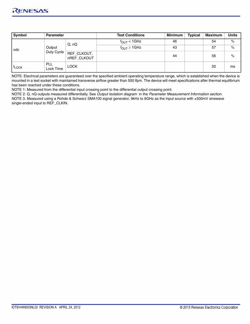
NOTE: Electrical parameters are guaranteed over the specified ambient operating temperature range, which is established when the device is mounted in a test socket with maintained transverse airflow greater than 500 lfpm. The device will meet specifications after thermal equilibrium has been reached under these conditions. NOTE 1: Measured from the differential input crossing point to the differential output crossing point. NOTE 2: Q, nQ outputs measured differentially. See Output Isolation diagram in the Parameter Measurement Information section. NOTE 3. Measured using a Rohde & Schwarz SMA100 signal generator, 9kHz to 6GHz as the input source with ±500mV sinewave single-ended input to REF_CLKIN.
odcOutput Duty Cycle
Q, nQfOUT < 1GHz 46 54 %
fOUT ≥ 1GHz 43 57 %
REF_CLKOUT,nREF_CLKOUT
44 56 %
tLOCKPLL Lock Time
LOCK 20 ms
Symbol Parameter Test Conditions Minimum Typical Maximum Units

IDT8V44N003NLGI REVISION A APRIL 24, 2012 13 ©2012 Integrated Device Technology, Inc.
IDT8V44N003I Data Sheet FEMTOCLOCK® NG LVDS CLOCK SYNTHESIZER
Single Side Band Noise Power (80MHz)
SS
B P
has
e N
ois
e d
Bc/
Hz
Offset from Carrier Frequency (Hz)

IDT8V44N003NLGI REVISION A APRIL 24, 2012 14 ©2012 Integrated Device Technology, Inc.
IDT8V44N003I Data Sheet FEMTOCLOCK® NG LVDS CLOCK SYNTHESIZER
RMS Phase Jitter (480MHz)
SS
B P
has
e N
ois
e d
Bc/
Hz
Offset from Carrier Frequency (Hz)
IDT8V44N003NLGI REVISION A APRIL 24, 2012 15 ©2012 Integrated Device Technology, Inc.
IDT8V44N003I Data Sheet FEMTOCLOCK® NG LVDS CLOCK SYNTHESIZER
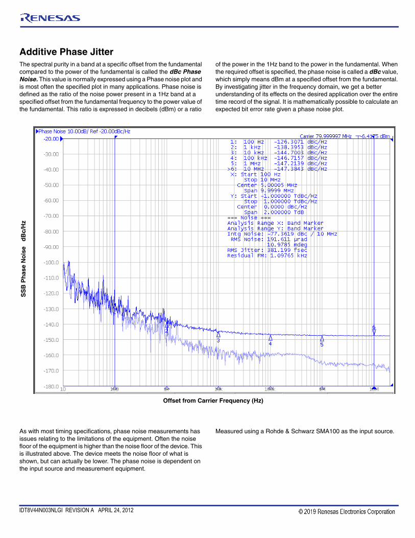
Additive Phase JitterThe spectral purity in a band at a specific offset from the fundamental compared to the power of the fundamental is called the dBc Phase Noise. This value is normally expressed using a Phase noise plot and is most often the specified plot in many applications. Phase noise is defined as the ratio of the noise power present in a 1Hz band at a specified offset from the fundamental frequency to the power value of the fundamental. This ratio is expressed in decibels (dBm) or a ratio
of the power in the 1Hz band to the power in the fundamental. When the required offset is specified, the phase noise is called a dBc value, which simply means dBm at a specified offset from the fundamental. By investigating jitter in the frequency domain, we get a better understanding of its effects on the desired application over the entire time record of the signal. It is mathematically possible to calculate an expected bit error rate given a phase noise plot.
As with most timing specifications, phase noise measurements has issues relating to the limitations of the equipment. Often the noise floor of the equipment is higher than the noise floor of the device. This is illustrated above. The device meets the noise floor of what is shown, but can actually be lower. The phase noise is dependent on the input source and measurement equipment.
Measured using a Rohde & Schwarz SMA100 as the input source.
SS
B P
has
e N
ois
e d
Bc/
Hz
Offset from Carrier Frequency (Hz)

IDT8V44N003NLGI REVISION A APRIL 24, 2012 16 ©2012 Integrated Device Technology, Inc.
IDT8V44N003I Data Sheet FEMTOCLOCK® NG LVDS CLOCK SYNTHESIZER
Parameter Measurement Information
3.3V LVDS Output Load AC Test Circuit
Propagation Delay
Output Isolation (Q, nQ (480MHz) to ±REF_CLKOUT, nREF_CLKOUT)
Differential Input Level
RMS Phase Jitter
Output Isolation
SCOPEQx
nQx
3.3V±5% POWER SUPPLY+ –Float GND
VDDA
VDD
tPD
nREF_CLKIN
REF_CLKIN
nREF_CLKOUT
REF_CLKOUT
Am
plitu
de (
dB)
A0
Spectrum of Output Signal Q
Output_ISOL = A0 – A1
(fundamental)Frequencyƒ
–REF_CLKOUT,nREF_CLKOUT
+REF_CLKOUT,nREF_CLKOUT
Q0, nQ0
A1
nREF_CLKIN
VDD
GND
VCMR
Cross PointsVPP
REF_CLKIN
Offset Frequencyf1 f2
Phase Noise Plot
RMS Jitter = Area Under Curve Defined by the Offset Frequency Markers
Noi
se P
ower
Am
plitu
de (
dB)
A0
(fundamental)Frequencyƒ
Output selects static input
Output selects activeinput clock signal
A1
Spectrum of Output Signal QQ0, nQ0
Output_ISOL = A0 – A1

IDT8V44N003NLGI REVISION A APRIL 24, 2012 17 ©2012 Integrated Device Technology, Inc.
IDT8V44N003I Data Sheet FEMTOCLOCK® NG LVDS CLOCK SYNTHESIZER
Parameter Measurement Information, continued
LVDS Output Duty Cycle/Pulse Width/Period
Differential Output Voltage Setup
PLL Lock Time
LVDS Output Rise/Fall Time
Offset Voltage Setup
tPW
tPERIOD
tPW
tPERIOD
odc = x 100%
nQ,nREF_CLKOUT
Q,REF_CLKOUT
100
out
out
LVDSDC Input VOD/∆ VOD
VDD
20%
80% 80%
20%
tR tF
VOD
nQ,nREF_CLKOUT
Q,REF_CLKOUT
out
out
LVDSDC Input
VOS/∆ VOS
VDD
IDT8V44N003NLGI REVISION A APRIL 24, 2012 18 ©2012 Integrated Device Technology, Inc.
IDT8V44N003I Data Sheet FEMTOCLOCK® NG LVDS CLOCK SYNTHESIZER
Applications Information
Recommendations for Unused Input and Output Pins
Inputs:
LVCMOS Control PinsAll control pins have internal pullups or pulldowns; additional resistance is not required but can be added for additional protection. A 1kΩ resistor can be used.
Outputs:
LVDS OutputsAll unused LVDS output pairs can be either left floating or terminated with 100Ω across. If they are left floating, we recommend that there
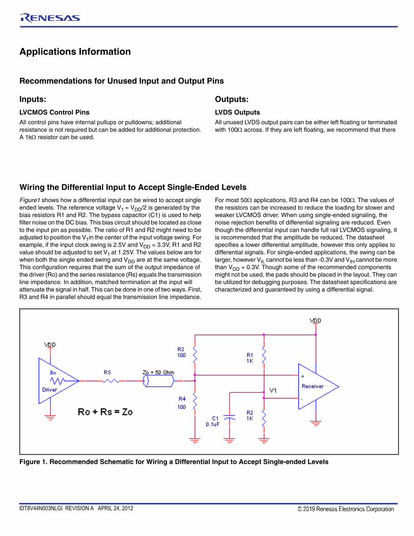
Wiring the Differential Input to Accept Single-Ended Levels
Figure1 shows how a differential input can be wired to accept single ended levels. The reference voltage V1 = VDD/2 is generated by the bias resistors R1 and R2. The bypass capacitor (C1) is used to help filter noise on the DC bias. This bias circuit should be located as close to the input pin as possible. The ratio of R1 and R2 might need to be adjusted to position the V1in the center of the input voltage swing. For example, if the input clock swing is 2.5V and VDD = 3.3V, R1 and R2 value should be adjusted to set V1 at 1.25V. The values below are for when both the single ended swing and VDD are at the same voltage. This configuration requires that the sum of the output impedance of the driver (Ro) and the series resistance (Rs) equals the transmission line impedance. In addition, matched termination at the input will attenuate the signal in half. This can be done in one of two ways. First, R3 and R4 in parallel should equal the transmission line impedance.
For most 50Ω applications, R3 and R4 can be 100Ω. The values of the resistors can be increased to reduce the loading for slower and weaker LVCMOS driver. When using single-ended signaling, the noise rejection benefits of differential signaling are reduced. Even though the differential input can handle full rail LVCMOS signaling, it is recommended that the amplitude be reduced. The datasheet specifies a lower differential amplitude, however this only applies to differential signals. For single-ended applications, the swing can be larger, however VIL cannot be less than -0.3V and VIH cannot be more than VDD + 0.3V. Though some of the recommended components might not be used, the pads should be placed in the layout. They can be utilized for debugging purposes. The datasheet specifications are characterized and guaranteed by using a differential signal.
Figure 1. Recommended Schematic for Wiring a Differential Input to Accept Single-ended Levels

IDT8V44N003NLGI REVISION A APRIL 24, 2012 19 ©2012 Integrated Device Technology, Inc.
IDT8V44N003I Data Sheet FEMTOCLOCK® NG LVDS CLOCK SYNTHESIZER
3.3V LVPECL Clock Input Interface
The REF_CLK/nREF_CLK accepts LVPECL, LVDS, HCSL and other differential signals. Both differential signals must meet the VPP and VCMR input requirements. Figures 2A to 2D show interface examples for the REF_CLK/nREF_CLK input driven by the most common driver
types. The input interfaces suggested here are examples only. If the driver is from another vendor, use their termination recommendation. Please consult with the vendor of the driver component to confirm the driver termination requirements.
Figure 2A. REF_CLK/nREF_CLK Input Driven by a 3.3V LVPECL Driver
3.3V
R31k
R41k
R11k
R21k
3.3VZo = 50Ω
Zo = 50Ω
3.3V
C1
C2R5100
LVDS
REF_CLK
nREF_CLK
LVPECLInput
Figure 2C. REF_CLK/nREF_CLK Input Driven by a 3.3V LVDS Driver
R384
R484
R1125
R2125
R5100 - 200
R6100 - 200
3.3V LVPECL
3.3V
Zo = 50Ω
Zo = 50Ω
3.3V
3.3V
C1
C2
REF_CLK
nREF_CLK
LVPECLInput
Figure 2B. REF_CLK/nREF_CLK Input Driven by a 3.3V LVPECL Driver with AC Couple
Figure 2D. REF_CLK/nREF_CLK Input Driven by a 3.3V HCSL Driver
R3125
R4125
R184
R284
3.3V
Zo = 50Ω
Zo = 50Ω
3.3V3.3V
LVPECL
REF_CLK
nREF_CLK
LVPECLInput
HCSL
*R3 33Ω
*R4 33Ω
REF_CLK
nREF_CLK
3.3V 3.3V
Zo = 50Ω
Zo = 50Ω
Differential InputR1
50ΩR250Ω
*Optional – R3 and R4 can be 0Ω

IDT8V44N003NLGI REVISION A APRIL 24, 2012 20 ©2012 Integrated Device Technology, Inc.
IDT8V44N003I Data Sheet FEMTOCLOCK® NG LVDS CLOCK SYNTHESIZER
LVDS Driver Termination
A general LVDS interface is shown in Figure 3A. Standard termination for LVDS type output structure requires both a 100Ω parallel resistor at the receiver and a 100Ω differential transmission line environment. In order to avoid any transmission line reflection issues, the 100Ω resistor must be placed as close to the receiver as possible. IDT offers a full line of LVDS compliant devices with two types of output structures: current source and voltage source. The standard
termination schematic as shown in Figure 3A can be used with either type of output structure. If using a non-standard termination, it is recommended to contact IDT and confirm if the output is a current source or a voltage source type structure. In addition, since these outputs are LVDS compatible, the amplitude and common mode input range of the input receivers should be verified for compatibility with the output.
LVDS Driver Termination
LVDS Driver
LVDS Driver
LVDS Receiver
LVDS ReceiverZT
C
ZO ≈ ZT
ZO ≈ ZT
ZT2
ZT2
Figure 3A. Standard Termination
Figure 3B. Optional Termination
IDT8V44N003NLGI REVISION A APRIL 24, 2012 21 ©2012 Integrated Device Technology, Inc.
IDT8V44N003I Data Sheet FEMTOCLOCK® NG LVDS CLOCK SYNTHESIZER
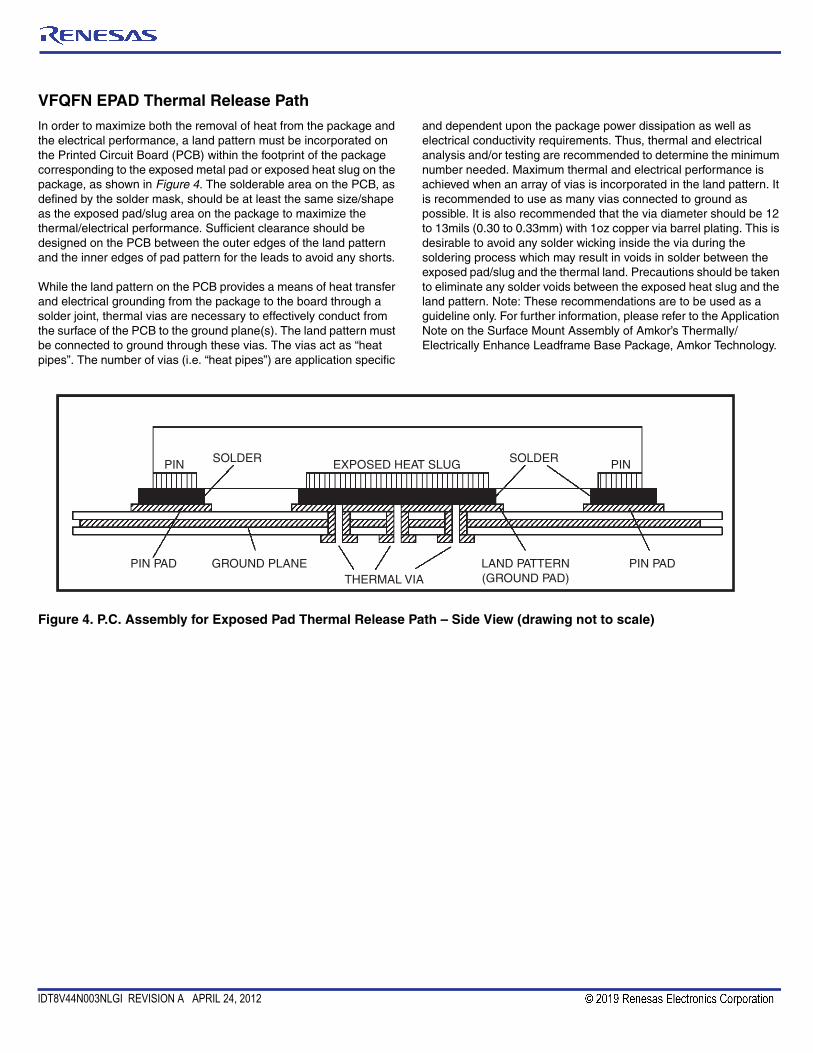
VFQFN EPAD Thermal Release Path
In order to maximize both the removal of heat from the package and the electrical performance, a land pattern must be incorporated on the Printed Circuit Board (PCB) within the footprint of the package corresponding to the exposed metal pad or exposed heat slug on the package, as shown in Figure 4. The solderable area on the PCB, as defined by the solder mask, should be at least the same size/shape as the exposed pad/slug area on the package to maximize the thermal/electrical performance. Sufficient clearance should be designed on the PCB between the outer edges of the land pattern and the inner edges of pad pattern for the leads to avoid any shorts.
While the land pattern on the PCB provides a means of heat transfer and electrical grounding from the package to the board through a solder joint, thermal vias are necessary to effectively conduct from the surface of the PCB to the ground plane(s). The land pattern must be connected to ground through these vias. The vias act as “heat pipes”. The number of vias (i.e. “heat pipes”) are application specific
and dependent upon the package power dissipation as well as electrical conductivity requirements. Thus, thermal and electrical analysis and/or testing are recommended to determine the minimum number needed. Maximum thermal and electrical performance is achieved when an array of vias is incorporated in the land pattern. It is recommended to use as many vias connected to ground as possible. It is also recommended that the via diameter should be 12 to 13mils (0.30 to 0.33mm) with 1oz copper via barrel plating. This is desirable to avoid any solder wicking inside the via during the soldering process which may result in voids in solder between the exposed pad/slug and the thermal land. Precautions should be taken to eliminate any solder voids between the exposed heat slug and the land pattern. Note: These recommendations are to be used as a guideline only. For further information, please refer to the Application Note on the Surface Mount Assembly of Amkor’s Thermally/ Electrically Enhance Leadframe Base Package, Amkor Technology.
Figure 4. P.C. Assembly for Exposed Pad Thermal Release Path – Side View (drawing not to scale)
SOLDERSOLDER PINPIN EXPOSED HEAT SLUG
PIN PAD PIN PADGROUND PLANE LAND PATTERN (GROUND PAD)THERMAL VIA

IDT8V44N003NLGI REVISION A APRIL 24, 2012 22 ©2012 Integrated Device Technology, Inc.
IDT8V44N003I Data Sheet FEMTOCLOCK® NG LVDS CLOCK SYNTHESIZER
Schematic ExampleFigure 5 shows an example of IDT8V44N003I application schematic. Input and output terminations shown are intended as examples only and may not represent the exact user configuration.
As with any high speed analog circuitry, the power supply pins are vulnerable to noise. To achieve optimum jitter performance, power supply isolation is required. The IDT8V44N003I provides separate power VDD and VDDA power supplies to isolate from coupling into the internal PLL.
In order to achieve the best possible filtering, it is recommended that the placement of the filter components be on the device side of the PCB as close to the power pins as possible. If space is limited, the
0.1uF capacitor in each power pin filter should be placed on the device side of the PCB and the other components can be placed on the opposite side.
Power supply filter recommendations are a general guideline to be used for reducing external noise from coupling into the devices. The filter performance is designed for wide range of noise frequencies. This low-pass filter starts to attenuate noise at approximately 10kHz. If a specific frequency noise component is known, such as switching power supply frequencies, it is recommended that component values be adjusted and if required, additional filtering be added. Additionally, good general design practices for power plane voltage stability suggests adding bulk capacitances in the local area of all devices.
C70.1uF
VDD_27
VDDA
VDD_27
Zo = 50 Ohm
Zo = 50 Ohm
Zo = 50 Ohm
C60.1uF
C100.1uF
3.3V
C14
10uF
FB1
BLM18BB221SN1
1 2
3.3V
C16
10uF
FB2
BLM18BB221SN1
12
C190.1uF
SDATASCLK
VDD_23
Zo = 50 Ohm
R4 50
R550
Zo = 50 OhmR3 50
C810uF
R6
10
R14.7K
3.3V
R24.7K
C150.1uF
Zo = 50 Ohm
U1
VDD27
VPP3
nc1
nc4
nQ20
Q21
REF_CLKOUT16
nREF_CLKOUT15
nc28
nc31
GND6
REF_CLKIN13
nREF_CLKIN12
nc22
nc11
nc17
GND18
VDD23
GND10
Reserved2
nc5
GND8
LOCK14
VDDA25
SDATA29
SCLK32
GND30
nc9nc7
nc24
nc26
nc19
epad33
VDD_23
PECL Driver
LOCK
LVDS Receiver
+
-
LVDS Receiver
+
-
R17100
R18100
R7
330
VDDA
Figure 5. IDT8V44N003I Application Schematic

IDT8V44N003NLGI REVISION A APRIL 24, 2012 23 ©2012 Integrated Device Technology, Inc.
IDT8V44N003I Data Sheet FEMTOCLOCK® NG LVDS CLOCK SYNTHESIZER
Power ConsiderationsThis section provides information on power dissipation and junction temperature for the IDT8V44N003I. Equations and example calculations are also provided.
1. Power Dissipation.
The total power dissipation for the IDT8V44N003I is the sum of the core power plus the analog power plus the power dissipated in the load(s). The following is the power dissipation for VDD = 3.3V + 5% = 3.465V, which gives worst case results.
• Power (core)MAX = VDD_MAX * (IDD_MAX + IDDA_MAX) = 3.465V * (136mA + 17mA) = 530.145mW
2. Junction Temperature.
Junction temperature, Tj, is the temperature at the junction of the bond wire and bond pad directly affects the reliability of the device. The maximum recommended junction temperature is 125°C. Limiting the internal transistor junction temperature, Tj, to 125°C ensures that the bond wire and bond pad temperature remains below 125°C.
The equation for Tj is as follows: Tj = θJA * Pd_total + TA
Tj = Junction Temperature
θJA = Junction-to-Ambient Thermal Resistance
Pd_total = Total Device Power Dissipation (example calculation is in section 1 above)
TA = Ambient Temperature
In order to calculate junction temperature, the appropriate junction-to-ambient thermal resistance θJA must be used. Assuming no air flow and a multi-layer board, the appropriate value is 43.7°C/W per Table 6 below.
Therefore, Tj for an ambient temperature of 85°C with all outputs switching is:
85°C + 0.530W * 43.7°C/W = 108.2°C. This is below the limit of 125°C.
This calculation is only an example. Tj will obviously vary depending on the number of loaded outputs, supply voltage, air flow and the type of board (multi-layer).
Table 6. Thermal Resistance θJA for 32 Lead VFQFN, Forced Convection
θJA by Velocity
Meters per Second 0 1 2.5
Multi-Layer PCB, JEDEC Standard Test Boards 43.7°C/W 38.2°C/W 34.2°C/W

IDT8V44N003NLGI REVISION A APRIL 24, 2012 24 ©2012 Integrated Device Technology, Inc.
IDT8V44N003I Data Sheet FEMTOCLOCK® NG LVDS CLOCK SYNTHESIZER
Reliability Information
Table 7. θJA vs. Air Flow Table for a 32 Lead VFQFN
Transistor Count
The transistor count for IDT8V44N003I is: 47,632
θJA vs. Air Flow
Meter per Second 0 1 2.5
Multi-Layer PCB, JEDEC Standard Test Boards 43.7°C/W 38.2°C/W 34.2°C/W

IDT8V44N003NLGI REVISION A APRIL 24, 2012 25 ©2012 Integrated Device Technology, Inc.
IDT8V44N003I Data Sheet FEMTOCLOCK® NG LVDS CLOCK SYNTHESIZER
Package Outline and Package Dimensions

IDT8V44N003NLGI REVISION A APRIL 24, 2012 26 ©2012 Integrated Device Technology, Inc.
IDT8V44N003I Data Sheet FEMTOCLOCK® NG LVDS CLOCK SYNTHESIZER
Ordering InformationTable 8. Ordering Information
NOTE: Parts that are ordered with an "G" suffix to the part number are the Pb-Free configuration and are RoHS compliant.
Part/Order Number Marking Package Shipping Packaging Temperature8V44N003NLGI IDT8V44N003NLGI “Lead-Free” 32 Lead VFQFN Tray -40°C to 85°C8V44N003NLGI8 IDT8V44N003NLGI “Lead-Free” 32 Lead VFQFN 2500 Tape & Reel -40°C to 85°C

IDT8V44N003NLGI REVISION A APRIL 24, 2012 27 ©2012 Integrated Device Technology, Inc.
IDT8V44N003I Data Sheet FEMTOCLOCK® NG LVDS CLOCK SYNTHESIZER
Revision History Sheet
Rev Table Page Description of Change Date
A 2 Corrected block diagram, missing line from PFD to VCO to mux. 4/24/12

DISCLAIMER Integrated Device Technology, Inc. (IDT) and its subsidiaries reserve the right to modify the products and/or specifications described herein at any time and at IDT’s sole discretion. All information in this document, including descriptions of product features and performance, is subject to change without notice. Performance specifications and the operating parameters of the described products are determined in the independent state and are not guaranteed to perform the same way when installed in customer products. The information contained herein is provided without representation or warranty of any kind, whether express or implied, including, but not limited to, the suitability of IDT’s products for any particular purpose, an implied warranty of merchantability, or non-infringement of the intellectual property rights of others. This document is presented only as a guide and does not convey any license under intellectual property rights of IDT or any third parties.
IDT’s products are not intended for use in life support systems or similar devices where the failure or malfunction of an IDT product can be reasonably expected to significantly affect the health or safety of users. Anyone using an IDT product in such a manner does so at their own risk, absent an express, written agreement by IDT.
Integrated Device Technology, IDT and the IDT logo are registered trademarks of IDT. Other trademarks and service marks used herein, including protected names, logos and designs, are the property of IDT or their respective third party owners.
Copyright 2012. All rights reserved.
6024 Silver Creek Valley Road San Jose, California 95138
Sales800-345-7015 (inside USA)+408-284-8200 (outside USA)Fax: 408-284-2775www.IDT.com/go/contactIDT
Technical [email protected]+480-763-2056
We’ve Got Your Timing Solution
IDT8V44N003I Data Sheet FEMTOCLOCK® NG LVDS CLOCK SYNTHESIZER

Corporate HeadquartersTOYOSU FORESIA, 3-2-24 Toyosu,Koto-ku, Tokyo 135-0061, Japanwww.renesas.com
Contact InformationFor further information on a product, technology, the most up-to-date version of a document, or your nearest sales office, please visit:www.renesas.com/contact/
TrademarksRenesas and the Renesas logo are trademarks of Renesas Electronics Corporation. All trademarks and registered trademarks are the property of their respective owners.
IMPORTANT NOTICE AND DISCLAIMER
RENESAS ELECTRONICS CORPORATION AND ITS SUBSIDIARIES (“RENESAS”) PROVIDES TECHNICAL SPECIFICATIONS AND RELIABILITY DATA (INCLUDING DATASHEETS), DESIGN RESOURCES (INCLUDING REFERENCE DESIGNS), APPLICATION OR OTHER DESIGN ADVICE, WEB TOOLS, SAFETY INFORMATION, AND OTHER RESOURCES “AS IS” AND WITH ALL FAULTS, AND DISCLAIMS ALL WARRANTIES, EXPRESS OR IMPLIED, INCLUDING, WITHOUT LIMITATION, ANY IMPLIED WARRANTIES OF MERCHANTABILITY, FITNESS FOR A PARTICULAR PURPOSE, OR NON-INFRINGEMENT OF THIRD PARTY INTELLECTUAL PROPERTY RIGHTS.
These resources are intended for developers skilled in the art designing with Renesas products. You are solely responsible for (1) selecting the appropriate products for your application, (2) designing, validating, and testing your application, and (3) ensuring your application meets applicable standards, and any other safety, security, or other requirements. These resources are subject to change without notice. Renesas grants you permission to use these resources only for development of an application that uses Renesas products. Other reproduction or use of these resources is strictly prohibited. No license is granted to any other Renesas intellectual property or to any third party intellectual property. Renesas disclaims responsibility for, and you will fully indemnify Renesas and its representatives against, any claims, damages, costs, losses, or liabilities arising out of your use of these resources. Renesas' products are provided only subject to Renesas' Terms and Conditions of Sale or other applicable terms agreed to in writing. No use of any Renesas resources expands or otherwise alters any applicable warranties or warranty disclaimers for these products.
(Rev.1.0 Mar 2020)
© 2020 Renesas Electronics Corporation. All rights reserved.