Embed Size (px)
Citation preview
Ferroelectric Tunnel Junctions
I n a u g u r a l – D i s s e r t a t i o n
zur
Erlangung des Doktorgrades
der Mathematisch-Naturwissenschaftlichen Fakultät
der Universität zu Köln
vorgelegt von
Julio Rodríguez Contreras aus Hürth
Eigenverlag Forschungszentrum Jülich, Jülich, 2004
Berichterstatter: Prof. Dr. Ch. Buchal Prof. Dr. M. Braden
Tag der mündlichn Prüfung: 10. November 2003

Kurzzusammenfassung
Ferroelektrizitat und quantenmechanisches Elektronentunneln sind gut be-kannte physikalische Phanomene, die seit einem Jahrhundert untersucht wer-den. Wahrend dieser langen Zeit beschaftigte sich die wissenschaftlicheForschung entweder mit Ferroelektrizitat oder mit dem Elektronentunneln.Niemals zuvor hat eine Verbindung dieser beiden Phanomene stattgefundenund niemals ist ein neues Phanomen beobachtet worden, das auf ihrer Wech-selwirkung beruht.
In dieser Arbeit stelle ich das Konzept eines ferroelektrischen Tunnelkon-takts vor. Der Begriff ferroelektrisch bezieht sich hierbei auf eine Eigenschaftdes Barrierenmaterials. Ein solcher Tunnelkontakt besteht aus einer ferro-elektrischen Schicht, die sich zwischen zwei Metallelektroden befindet. Dieferroelektrische Schicht ist dabei dunn genug, um Elektronentunneln durchsie hindurch zu ermoglichen.
Zum ersten Mal wird die Wechselwirkung von makroskopischen Großen,wie z. B. der spontanen Polarisation und der Gitterverzerrung, mit quanten-mechanischem Elektronentunneln experimentell untersucht.
Begleitet wird die experimentelle Arbeit durch theoretische Ideen undVorhersagen uber den Einfluß der Piezo- und Ferroelektrizitat auf das di-rekte Elektronentunneln.
Abstract
Ferroelectricity and quantum-mechanical electron tunneling are well-knownphysical phenomena that have been studied for as long as a century. Duringthis long period, scientific research has been restricted either to ferroelectric-ity or to electron tunneling. Never before have these subjects been combinedinto a new phenomenon based on their interaction.
Within this work, I present the novel concept of a ferroelectric tunneljunction, where the term ferroelectric refers to a property of the barrier ma-terial. This device consists of a ferroelectric layer sandwiched between metalelectrodes. The thickness of the ferroelectric layer is thin enough to allow forelectron tunneling.
For the first time, the influence of macroscopic parameters, such as thespontaneous polarization and strain on quantum-mechanical electron tunnel-ing through a ferroelectric tunnel barrier is studied experimentally.
In addition, the experimental work is accompanied by theoretical ideasand predictions concerning the manifestation of piezoelectricity or ferroelec-tricity in direct electron tunneling.

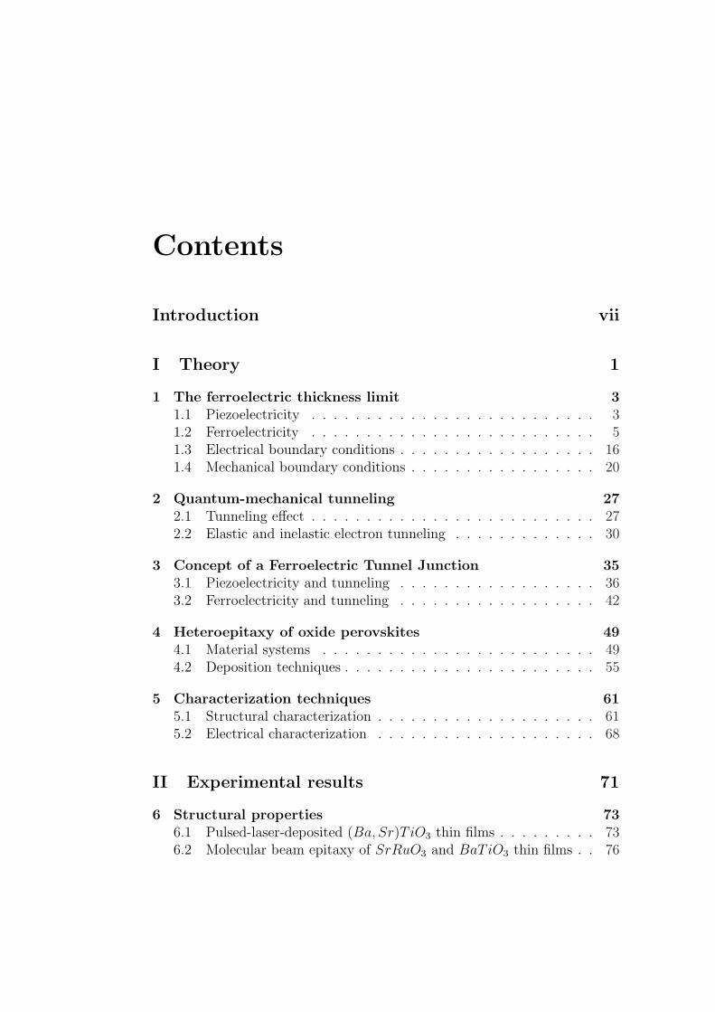
Contents
Introduction vii
I Theory 1
1 The ferroelectric thickness limit 31.1 Piezoelectricity . . . . . . . . . . . . . . . . . . . . . . . . . . 31.2 Ferroelectricity . . . . . . . . . . . . . . . . . . . . . . . . . . 51.3 Electrical boundary conditions . . . . . . . . . . . . . . . . . . 161.4 Mechanical boundary conditions . . . . . . . . . . . . . . . . . 20
2 Quantum-mechanical tunneling 272.1 Tunneling effect . . . . . . . . . . . . . . . . . . . . . . . . . . 272.2 Elastic and inelastic electron tunneling . . . . . . . . . . . . . 30
3 Concept of a Ferroelectric Tunnel Junction 353.1 Piezoelectricity and tunneling . . . . . . . . . . . . . . . . . . 363.2 Ferroelectricity and tunneling . . . . . . . . . . . . . . . . . . 42
4 Heteroepitaxy of oxide perovskites 494.1 Material systems . . . . . . . . . . . . . . . . . . . . . . . . . 494.2 Deposition techniques . . . . . . . . . . . . . . . . . . . . . . . 55
5 Characterization techniques 615.1 Structural characterization . . . . . . . . . . . . . . . . . . . . 615.2 Electrical characterization . . . . . . . . . . . . . . . . . . . . 68
II Experimental results 71
6 Structural properties 736.1 Pulsed-laser-deposited (Ba, Sr)TiO3 thin films . . . . . . . . . 736.2 Molecular beam epitaxy of SrRuO3 and BaTiO3 thin films . . 76
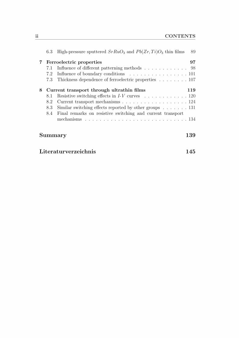
ii CONTENTS
6.3 High-pressure sputtered SrRuO3 and Pb(Zr, T i)O3 thin films 89
7 Ferroelectric properties 977.1 Influence of different patterning methods . . . . . . . . . . . . 987.2 Influence of boundary conditions . . . . . . . . . . . . . . . . 1017.3 Thickness dependence of ferroelectric properties . . . . . . . . 107
8 Current transport through ultrathin films 1198.1 Resistive switching effects in I-V curves . . . . . . . . . . . . 1208.2 Current transport mechanisms . . . . . . . . . . . . . . . . . . 1248.3 Similar switching effects reported by other groups . . . . . . . 1318.4 Final remarks on resistive switching and current transport
mechanisms . . . . . . . . . . . . . . . . . . . . . . . . . . . . 134
Summary 139
Literaturverzeichnis 145

Acknowledgements
Many people have provided me with assistance, guidance and support whileI was working on my PhD.
First, I am greatly indebted to Prof. Dr. Christoph Buchal for supervis-ing this thesis, for his support during the last three years and for our fruitfuldiscussions.
Thanks are also due to Prof. Dr. Markus Braden for accepting the taskof co-examiner. The interest he showed in my thesis is uncommon and isgreatly appreciated.
I wish to express my deepest gratitude to Dr. Hermann Kohlstedt for hisunwavering enthusiasm and his relentless pursuit of excellence. Hermann’scaring and support during my thesis are truly above and beyond the call ofduty. He deserves more than the traditional “thanks”.
I would like to thank Prof. Dr.-Ing. Rainer Waser for giving me the op-portunity to work on this thesis and for giving me the freedom and resourcesfrom which I greatly benefitted.
I am immensely grateful and deeply indebted to Prof. Dr. Darrell Schlomfor giving me the opportunity to spend nine awesome months at PennState.I am particularly grateful for Darrell’s generosity, his exceptional enthusiasmand for many inspiring and fascinating discussions.
Special mention deserves to be made of the continuous assistance pro-vided by Dr. Nicholas Pertsev. He contributed in a large manner to the workin this thesis. In addition, his critical comments on my draft are acknowl-edged with gratitude.

iv Acknowledgements
I also owe thanks to Dr. Jurgen Schubert for many inspiring discussions,for his support and for providing PLD-grown films.
I am obliged to Dr. Ulrich Poppe for his support with the high-pressuresputtering system and many stimulating discussions.
Special credit is also due to Bernd Hermanns for his contribution to thiswork during his diploma.
My special appreciation goes to Dr. Kristof Szot and Dr. Chunlin Jia forproviding AFM and HRTEM measurements, respectively. I am also gratefulto Dr. Theo Schneller, Daliborka Vukelic and Hans Haselier for providing Pttop electrodes.
I wish to express my sincere gratitude to Dr. James Lettieri, who recentlypassed away. My stay at PennState would not have been as exceptional asit was without James’ support and encouragement during this time. Ourdiscussions about science, sports and life are among my happiest memories.
Other members of the Schlom group who provided a relaxed atmosphereand continuous entertainment (inside and outside the lab) were Dr. JeffHaeni, Goh Asayama, Mike Biegalski, Dr. Venu Vaithyanathan, Lisa Fried-man Edge, and Sven Clemens.
I would also like to thank all colleagues at Research Center Julich andRWTH Aachen, including my office-mates Simon Stein, Andreas Gerber,Martin Weides, and Dr. Vladimir G. Kukhar.
I owe special acknowledgements to the many extremely talented collabo-rators who I have had the pleasure working with including Prof. Dr. PhilippeGhosez, Dr. Javier Junquera, Prof. Dr. Chang-Beom Eom, Prof. Dr. Ra-mamoorthy Ramesh, Dr. V. Nagarajan, Dr. Wei Tian, Prof. Dr. XiaoqingPan, Dr. Christian Loppacher, Dr. Frank Schlaphof, Prof. Dr. Lukas Eng,Dr. Klaus Michael Indlekofer, Dr. Stephan Tiedke and aixACCT Systems.
Acknowledgements v
Thanks are also due to Carol and Martin Stoffel, Janet Carter-Sigglow,Dr. Bernd Hollander, and Dr. Peter Ehrhart for their careful reading of sev-eral Chapters of this thesis.
I acknowledge the valuable role played by my high-school teacher, BrunoTuchscherer, who introduced me to the world of physics. His enthusiasticand fascinating teaching made a lasting impact on me.
I am indebted to the German Academic Exchange Service (DAAD), whosupported my stay at PennState University.
On a personal note, I would like to express my deepest gratitude to mygirl-friend, Katrin Felusch, for her emotional support. My grandmother,Fidela Herrero Jimenez, took care of me when I wrote a good part of thisthesis at her place in Salamanca, Spain. My family has been my biggest giftin life. I have enjoyed love and constant support from my sister Susana, mymother Maria del Carmen, and my father Tomas.

Introduction
In the last few years, tremendous progress has been made in the investigationof the ferroelectric limit in thickness. This is partly due to the accelerating in-terest in ferroelectric materials for technological applications, and it is partlydue to the natural scientific interest in understanding and studying the limitsof physical phenomena.
Ferroelectricity is a collective phenomenon discovered at the beginning ofthe last century [1]. Thirty years ago Batra and Silverman [2] predicted theferroelectric minimum thickness to be around 400 nm. Since then the pre-dicted minimum thickness has been reduced continuously. This developmentis based on a better understanding of the electrical and mechanical boundaryconditions in ferroelectric thin films. Some of the most important contribu-tions came from Batra and coworkers [3], Kretschmer and Binder [4], andPertsev et al. [5]. Based on recently published theoretical studies by Zembil-gotov and coworkers using a thermodynamic theory [6], as well as on ab-initiocalculations performed by Ghosez and Junquera [7], ferroelectricity in thinfilms under favorable boundary conditions is believed to survive in epitaxialfilms as thin as a few nm.
The experimental progress in studying finite size effects (i.e. the depen-dence of ferroelectric properties on the sample size) has been quite remark-able as well, especially in the last five years. This progress mainly arisesfrom constructing experiments based on a better theoretical understandingof ferroelectricity and from improvements in the deposition techniques andanalytical methods. In 1999, Yanase and coworkers showed ferroelectricity in12 nm thick BaTiO3 films [8]. In the same year, Tybell and coworkers pre-sented scanning probe microscopy measurements claiming the demonstrationof ferroelectricity in 4 nm thick PbT iO3 thin films [9]. Recently, Streiffer andcoworkers found 180 stripe domains in 3 monolayers of PbT iO3 by in situgrazing-incidence x-ray scattering and predicted the existence of ferroelec-tricity in this only 1.2 nm thick film [11, 10].
viii Introduction
The pursuit of the ferroelectric minimum thickness has reached a thick-ness range where tunneling through these films may be expected.Quantum-mechanical electron tunneling through an insulating barrier is oneof the most amazing phenomena in physics. The so-called tunneling effecthas been studied for 80 years. In this long period, the combination of ferro-electricity and tunneling has never been experimentally investigated. Unlikeferroelectricity, the combination of magnetism and tunneling, as well as su-perconductivity and tunneling, are the origin of well-known effects knownas tunneling magnetoresistance (Juillere 1975 [12]) and the Josephson effect(Josephson 1962 [13]), respectively.
Magnetic tunnel junctions and superconducting tunnel junctions, as wellas their combination, have been studied in the past. The aim of this work isthe study of a possible interaction of ferroelectricity and electron tunneling.It should be stressed that unlike the term magnetic and the term supercon-ducting in magnetic tunnel junction and superconducting tunnel junction,respectively, which both refer to a property of the electrode material, in aferroelectric tunnel junction the collective phenomenon is situated in the bar-rier itself.
This thesis is organized as follows. In Chapter 1 piezoelectricity and ferro-electricity are introduced and various origins of size effects in ferroelectric thinfilms are discussed. Chapter 2 deals with the relevant theories on electrontunneling through a thin barrier. In Chapter 3 the concept of a ferroelectrictunnel junction is presented. In this Chapter some ideas and predictionsare given about how the ferroelectric polarization reversal and the conversepiezoelectric effect may interact with direct electron tunneling through an ul-trathin ferroelectric barrier. In Chapter 4 the studied material systems andthe different deposition techniques used in this work are reported. Chapter 5is about the characterization techniques that were employed to study boththe structural and electrical properties of the thin films. The results of theformer are shown in Chapter 6. In Chapter 7 and 8 a detailed report onthe studies of the electrical properties and current transport mechanisms isgiven. It also contains the fabrication procedures of ferroelectric capacitorsand tunnel junctions. Finally, the results obtained in Chapter 8 are evalu-ated and compared with the theoretical ideas and calculations presented inChapter 3.
Part I
Theory

Chapter 1
The ferroelectric thickness limit
The question of whether or not there is a ferroelectric minimum in lateraldimensions and in thickness is a subject of ongoing discussion for more than30 years. The pursuit for miniaturization in micro- and nanotechnology isa challenge that requires the knowledge and understanding of how reduceddimensions affect the physical properties of a particular material.
This Chapter will start with an introduction of piezoelectricity and ferro-electricity. Afterwards various origins of size effects in ferroelectric thin filmswill be discussed.
1.1 Piezoelectricity
A dielectric material can be polarized by application of an electric field ~E.The total surface charge density induced in the material by the applied fieldis given by the dielectric displacement vector:
Di = ε0Ei + Pi, (1.1)
where ε0 = 8.854× 10⁻¹² Fm−1 is the dielectric permittivity of vacuum,and ~P is the polarization.
A dielectric material is referred to as a piezoelectric material, if it can bepolarized, in addition to an electric field, by application of mechanical stress.
The direct piezoelectric effect describes the linear relationship betweenthe applied stress Xik and the resulting charge density Di:
Di = dijkXjk, (1.2)
where dijk represents a third-rank tensor of the piezoelectric coefficients.
4 The ferroelectric thickness limit
For this work, the converse piezoelectric effect is more important. Thiseffect describes the field-induced strain Sij in a piezoelectric material:
Sij = dijkEk. (1.3)
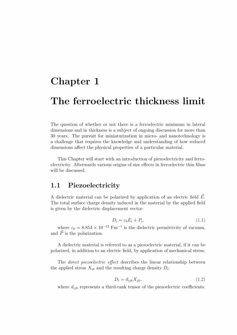
It can be shown that the piezoelectric coefficients for the direct and con-verse piezoelectric effect are identical [14]. For symmetry reasons the onlynon-zero piezoelectric coefficients are d333, d311 = d322 and d131 = d113 =d223 = d232 [15]. This tensor notation can, therefore, be simplified by in-troducing the matrix notation [16]. Here, the above mentioned non zeropiezoelectric coefficients are referred to as longitudinal component d33,transverse component d31 = d32 and shear component d15 = d24, re-spectively (see Fig. 1.1).
U UEP PUEPS1 S1
S3
S3
S5
S5
(a) (b) (c)
Figure 1.1: Illustration of the three different non-zero piezoelectric coefficients
for a material with symmetry 8m: a) d33 for a dielectric displacement, if a stress
is applied in the same direction or, for a strain, if the electric field is acting in
the same direction. b) d31 for a dielectric displacement, if a stress is applied in
the perpendicular direction or, for a strain, if the electric field is acting in the
perpendicular direction. c) d15 for a dielectric displacement, if a shear stress is
applied or, for a shear strain, if the electric field is acting. [17]
The converse piezoelectric effect is different from electrostriction, observedin all dielectric materials, since the converse piezoelectric effect is linear inthe applied electric field. The electrostrictive effect is based on a non-linearcoupling between elastic and electric fields. The application of an electric fieldproduces strain, which will not change on reversal of the electric field, i.e. theeffect is quadratic. With the exception of so-called relaxor-ferroelectrics1, theelectrostrictive effect is relatively small.
1Relaxors (e.g. (Pb, La)(Zr, T i)O3) display a diffuse phase transition with a broadmaximum in the dielectric permittivity. Relaxors do not obey the Curie-Weiss behavior.
1.2 Ferroelectricity 5
1.2 Ferroelectricity
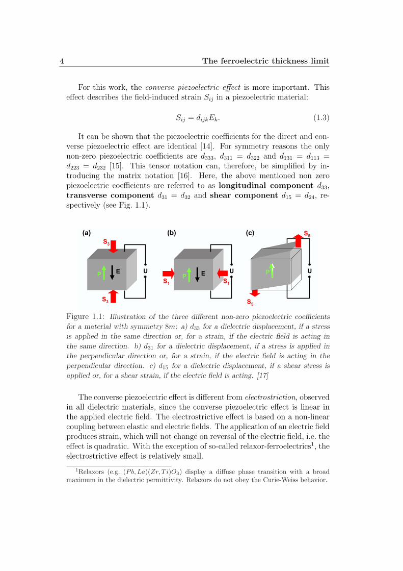
Figure 1.2 (a) schematically shows the displacement of the ions in an ABO3
perovskite structure due to an applied electric field. Ferroelectric materialsexhibit an electric dipole moment, even in the absence of an external elec-tric field. The polarization associated with the spontaneously formed dipolemoment is called spontaneous polarization ~PS. Ferroelectrics possess at leasttwo equilibrium orientations of the spontaneous polarization vector, ~PS. Thespontaneous polarization vector may be switched between those orientationsby application of an oppositely oriented electric field (see Fig. 1.2 (b)) [18].
PS
PS
E
E
Pb2+
Zr4+/ Ti4+
O2-
(a)
(b)
Figure 1.2: ABO3 perovskite structure, here Pb(Zr, T i)O3, under an external
electric field E applied along the polar axis (a) and in the opposite direction (b).
The hysteresis of the polarization P , as a function of the field E, is shownin Fig. 1.3 (a) for single-domain single crystals and in Fig. 1.3 (b) for polydo-main samples. The polarization at zero field is called remanent polarizationPr. It is identical to the spontaneous polarization for single domain sam-ples. In order to reverse the polarization, a coercive field Ec is necessary. Inpolydomain samples the field necessary to reduce the polarization to zero isreferred to as coercive field Ec.
I would like to point out that the polarization P , as well as the coercivefield Ec, are both macroscopic parameters.
Ferroelectric materials undergo a phase transition from a higher symme-try paraelectric phase to a lower symmetry ferroelectric phase. The paraelec-

6 The ferroelectric thickness limit
EcE
c
PS
Pr
Figure 1.3: Ferroelectric P-E curve for (a) single-domain and (b) polydomain
samples.
tric phase is not ferroelectric, but may be piezoelectric [18]. The temperature,where this phase transition occurs, is termed TC .
Mean-field theory
In order to calculate the phase transition, Landau [19] and Ginzburg [20] ex-panded the thermodynamical potential near the phase transition temperaturein a power series and introduced the spontaneous polarization as an orderparameter. Devonshire used this formalism, which assumes that the samepolynomial is capable of describing both ferroelectric and non-ferroelectricphases, to characterize the phase transition of BaTiO3 [21].
Following [17], the Ginzburg-Landau theory is equivalent to a mean fieldtheory, where the thermodynamic quantity - here, a dipole - is considered inthe mean field of all the others. Close to the phase transition temperature,the free energy F can be expanded in a power series with powers of the orderparameter P up to the sixth order:
F (P, T ) =1
2g2P
2 +1
4g4P
4 +1
6g6P
6 − P · E. (1.4)
No odd-power terms appear, as the polynomial has to be symmetricalagainst polarization reversal. The coefficients g2, g4, and g6 are in gen-eral temperature-dependent, but simple examples of first- and second-orderferroelectric phase transitions are described with g4 and g6 independent oftemperature [22]. Around the Curie-Weiss temperature T0, g2 can be ap-proximated by g2 = C−1(T − T0).
1.2 Ferroelectricity 7
The thermodynamically stable states are obtained from the minima ofthe free energy (with E = 0) via,
∂F
∂P= P (g2 + g4P
2 + g6P4) = 0, (1.5)
∂2F
∂2P= χ−1 = g2 + 3g4P
2 + 5g6P4 > 0. (1.6)
Equations (1.5, 1.6) are solved by P = 0 at g2 > 0. This is the para-electric (PE) phase. Other solutions exist for ±PS 6= 0. These are theferroelectric (FE) solutions.
Paraelectric phase
In the paraelectric phase, T > T0, the susceptibility is found to follow aCurie-Weiss law with a critical exponent γ = 1:
χ(T ) =C
T − T0
∝ (T − T0)−γ; γ = 1. (1.7)
First-order phase transition
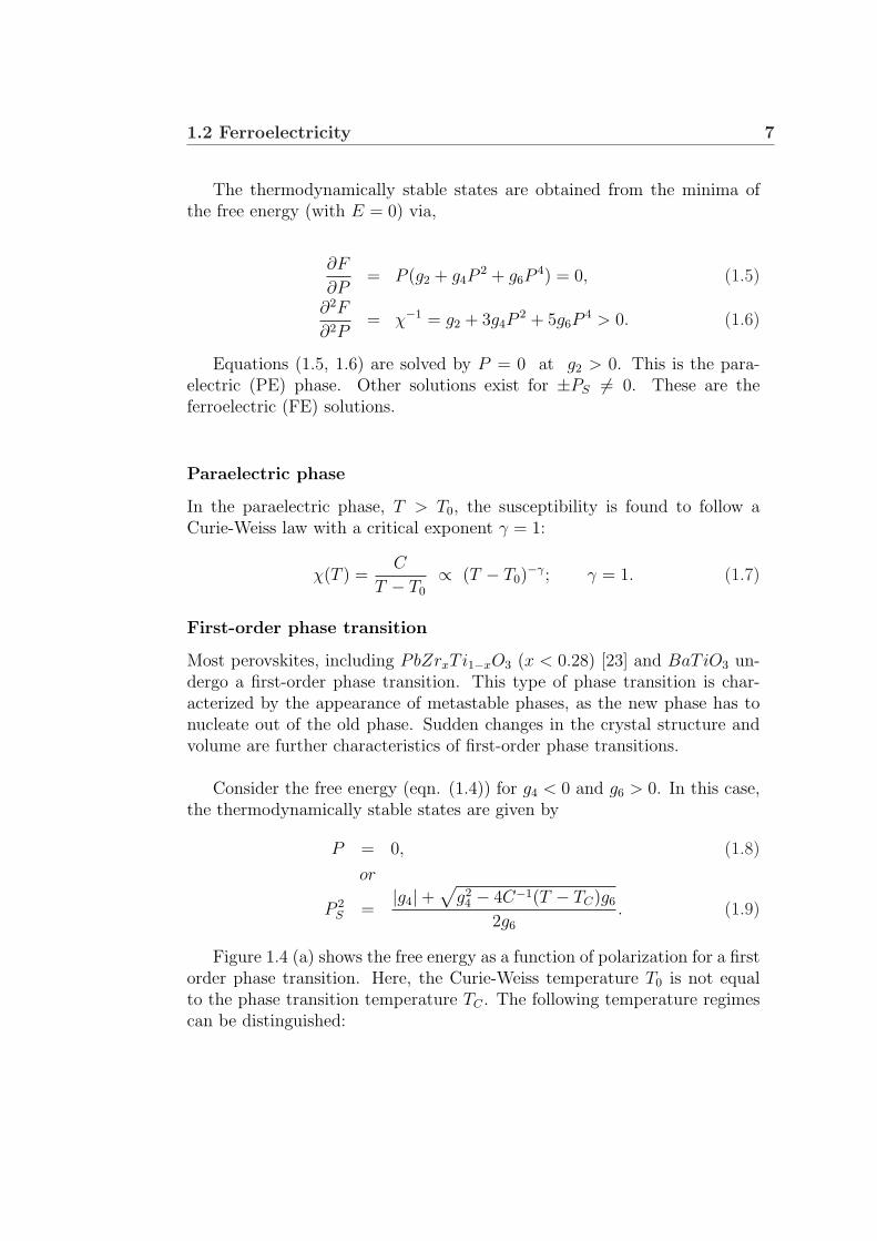
Most perovskites, including PbZrxTi1−xO3 (x < 0.28) [23] and BaTiO3 un-dergo a first-order phase transition. This type of phase transition is char-acterized by the appearance of metastable phases, as the new phase has tonucleate out of the old phase. Sudden changes in the crystal structure andvolume are further characteristics of first-order phase transitions.
Consider the free energy (eqn. (1.4)) for g4 < 0 and g6 > 0. In this case,the thermodynamically stable states are given by
P = 0, (1.8)
or
P 2S =
|g4|+√
g24 − 4C−1(T − TC)g6
2g6
. (1.9)
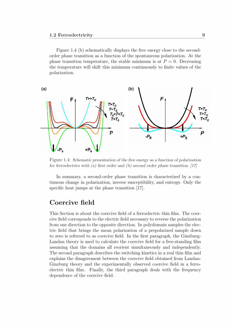
Figure 1.4 (a) shows the free energy as a function of polarization for a firstorder phase transition. Here, the Curie-Weiss temperature T0 is not equalto the phase transition temperature TC . The following temperature regimescan be distinguished:
8 The ferroelectric thickness limit
T À TC : stable paraelectric phase (P = 0)
T > TC : stable PE phase (P = 0), metastable FE phase (±PS 6= 0)
T = TC : coexistence of paraelectric and ferroelectric phase
T0 < T < TC : stable FE phase and metastable PE phase
T < T0: stable ferroelectric phase
Somewhere during the cooling through the regime where the paraelectricphase coexists with the metastable ferroelectric phase (T0 < T < TC), thesystem undergoes a transition with a discontinuity in the spontaneous polar-ization. In other words, the spontaneous polarization jumps from zero to afinite value corresponding with the first-order phase transition.
In addition, using the known thermodynamical relations, one will get atT = TC discontinuous changes in susceptibility χ and entropy S.
Second-order phase transition
Second-order phase transitions are characterized by a continuous change incrystal structure and volume. The first known ferroelectric material, Rochellesalt, NaKC4H4O6 · 4H2O [24], as well as PbZrxTi1−xO3 (x > 0.28) [23], un-dergo second-order phase transitions.
Here, it is sufficient to consider the polynomial expansion of the freeenergy (eqn. (1.4)) up to the fourth order and to take g4 > 0. From theseassumptions the following solutions are obtained:
P = 0, (1.10)
or
P 2S = − (T − TC)
g4C. (1.11)
Phase transition temperature TC and Curie-Weiss temperature T0 areidentical for a second-order phase transition. The critical exponent for theorder parameter is 1/2:
PS ∝ (T − TC)β; β = 1/2. (1.12)
1.2 Ferroelectricity 9
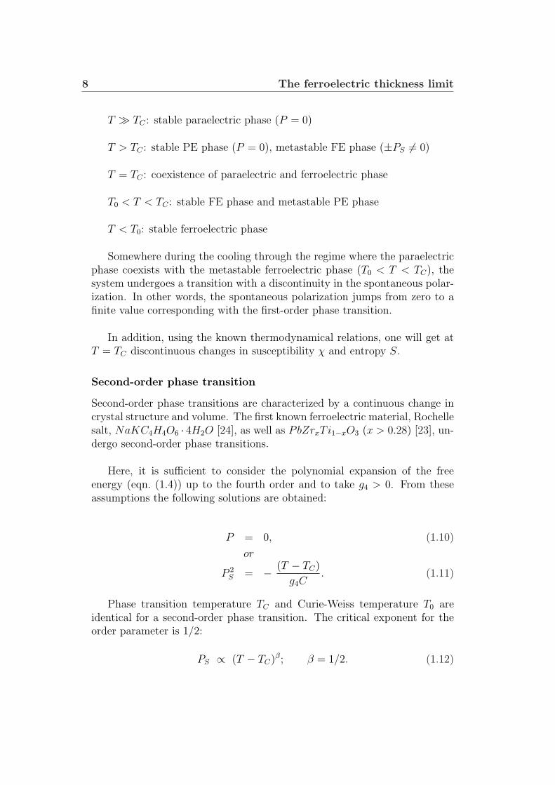
Figure 1.4 (b) schematically displays the free energy close to the second-order phase transition as a function of the spontaneous polarization. At thephase transition temperature, the stable minimum is at P = 0. Decreasingthe temperature will shift this minimum continuously to finite values of thepolarization.
(a) (b)
Figure 1.4: Schematic presentation of the free energy as a function of polarization
for ferroelectrics with (a) first order and (b) second order phase transition. [17]
In summary, a second-order phase transition is characterized by a con-tinuous change in polarization, inverse susceptibility, and entropy. Only thespecific heat jumps at the phase transition [17].
Coercive field
This Section is about the coercive field of a ferroelectric thin film. The coer-cive field corresponds to the electric field necessary to reverse the polarizationfrom one direction to the opposite direction. In polydomain samples the elec-tric field that brings the mean polarization of a prepolarized sample downto zero is referred to as coercive field. In the first paragraph, the Ginzburg-Landau theory is used to calculate the coercive field for a free-standing filmassuming that the domains all reorient simultaneously and independently.The second paragraph describes the switching kinetics in a real thin film andexplains the disagreement between the coercive field obtained from Landau-Ginzburg theory and the experimentally observed coercive field in a ferro-electric thin film. Finally, the third paragraph deals with the frequencydependence of the coercive field.
10 The ferroelectric thickness limit
Coercive field calculated from Ginzburg-Landau theory
Consider a polynomial expansion of the free energy (eqn. (1.4)) up to thefourth order [25] with the approximation for g2 given on page 6:
F (P, T ) =1
2C(T − TC)P 2 +
1
4g4P
4 − P · E. (1.13)
The conditions of thermodynamic equilibrium, which corresponds to theminimization of the free energy, are given by
∂F
∂P=
T − TC
CP + g4P
3 − E = 0, (1.14)
∂2F
∂P 2=
T − TC
C+ 3g4P
2 > 0. (1.15)
Equations (1.14, 1.15) are the necessary and sufficient conditions for aminimum of F (P ).
From eqn. (1.14) a 3rd order polynomial function is obtained:
E(P ) =T − TC
CP + g4P
3. (1.16)
The inversion of this function, excluding the parts that are not accessiblefor the system, gives the polarization hysteresis function P (E) (Fig. 1.5).The magnitude of the coercive field Ec can be calculated from the extremaof eqn. (1.16). The conditions
∂E
∂P=
T − TC
C+ 3g4P
2 = 0, (1.17)
∂2E
∂P 2= 6g4P 6= 0 ⇒ P 6= 0 (g4 6= 0, see p. 7), (1.18)
yield for T = 0 K
Pcr± = ±√
TC
3g4C. (1.19)
Pcr± corresponds to the polarization for the reversal fields at T = 0 K.Replacing P by Pcr in eqn. (1.16) yields the coercive field ( ~E ↑↓ ~P ):
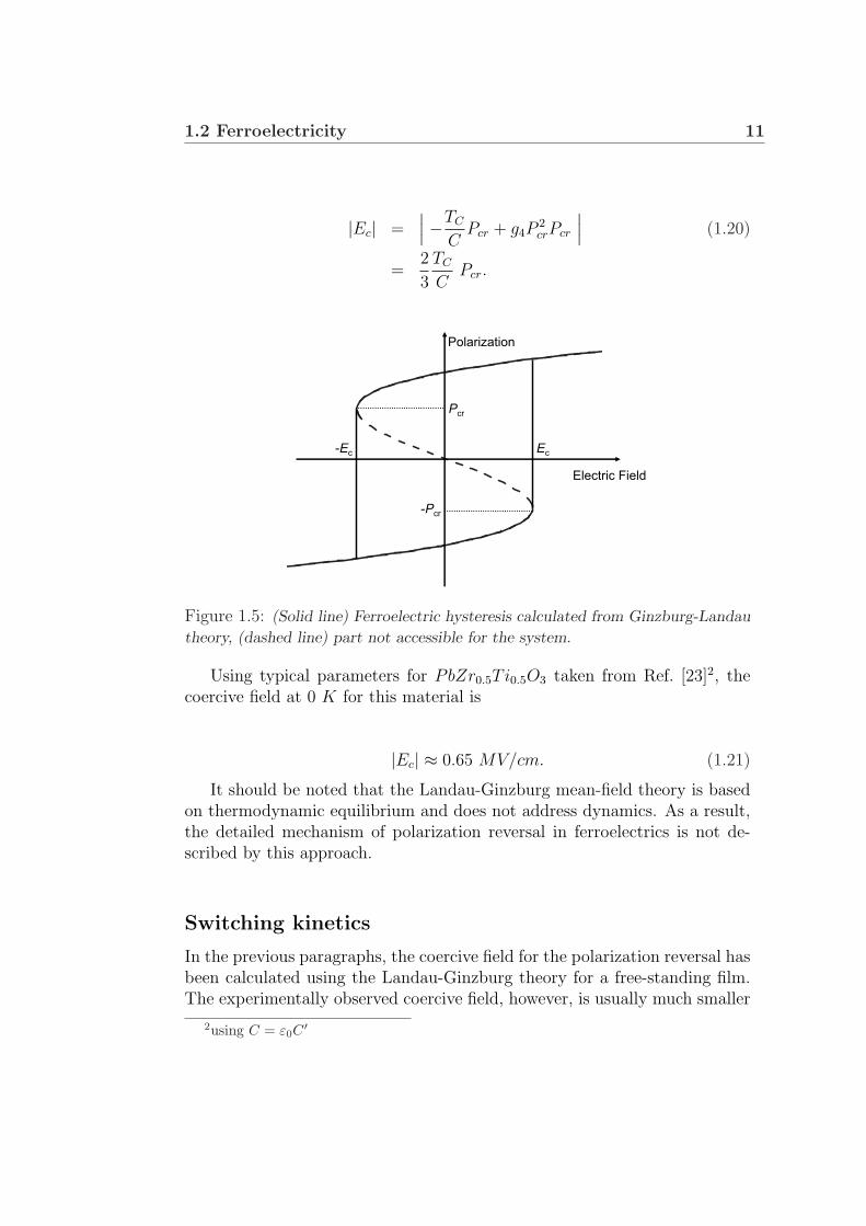
1.2 Ferroelectricity 11
|Ec| =∣∣∣ −TC
CPcr + g4P
2crPcr
∣∣∣ (1.20)
=2
3
TC
CPcr.
Electric Field
Polarization
Ec
-Ec
Pcr
-Pcr
Figure 1.5: (Solid line) Ferroelectric hysteresis calculated from Ginzburg-Landau
theory, (dashed line) part not accessible for the system.
Using typical parameters for PbZr0.5Ti0.5O3 taken from Ref. [23]2, thecoercive field at 0 K for this material is
|Ec| ≈ 0.65 MV/cm. (1.21)
It should be noted that the Landau-Ginzburg mean-field theory is basedon thermodynamic equilibrium and does not address dynamics. As a result,the detailed mechanism of polarization reversal in ferroelectrics is not de-scribed by this approach.
Switching kinetics
In the previous paragraphs, the coercive field for the polarization reversal hasbeen calculated using the Landau-Ginzburg theory for a free-standing film.The experimentally observed coercive field, however, is usually much smaller
2using C = ε0C′
12 The ferroelectric thickness limit
(about one order of magnitude in thin films and two orders of magnitude inbulk single crystals) - a result of dynamic processes not covered by the staticLandau-Ginzburg theory.
In most cases, it is energetically favorable to switch the polarization of adomain not simultaneously, but by moving the domain walls.
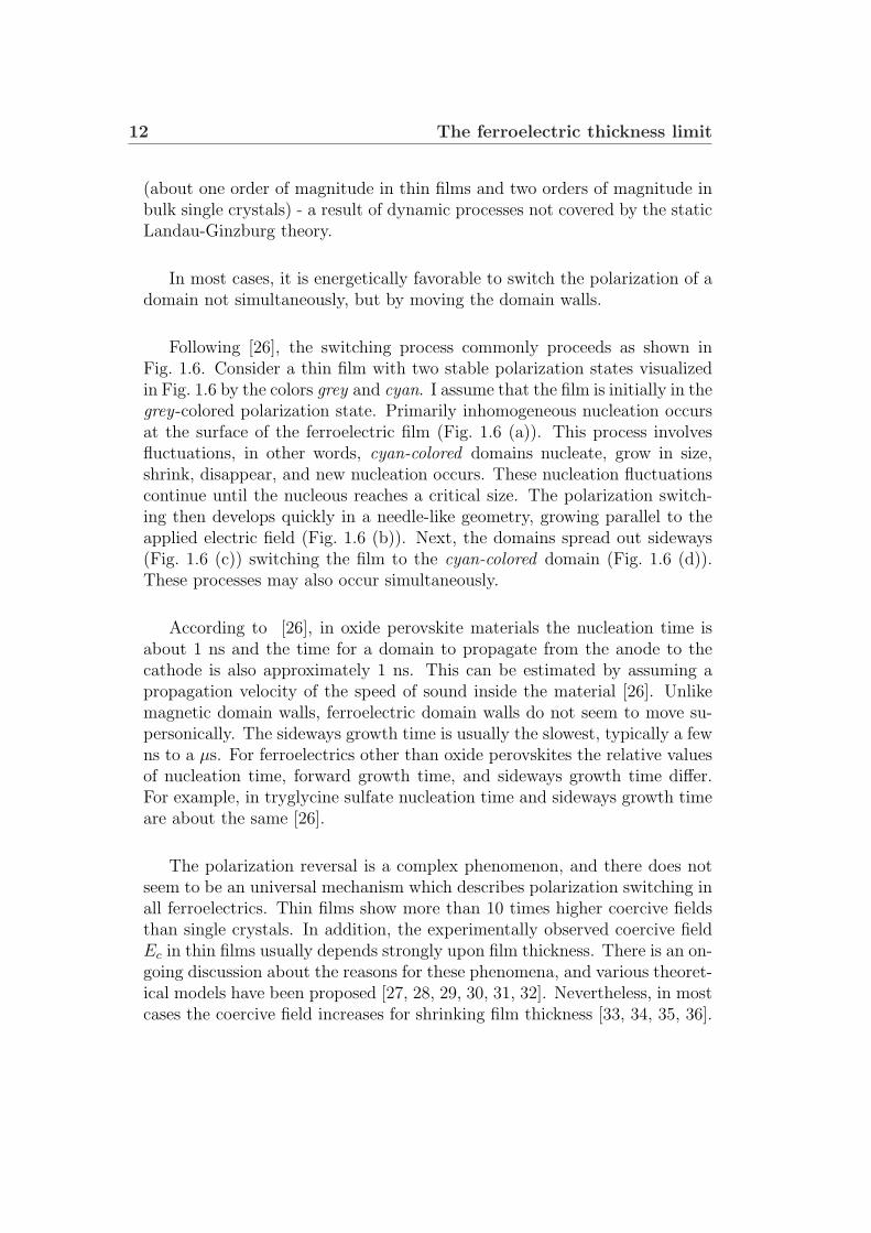
Following [26], the switching process commonly proceeds as shown inFig. 1.6. Consider a thin film with two stable polarization states visualizedin Fig. 1.6 by the colors grey and cyan. I assume that the film is initially in thegrey-colored polarization state. Primarily inhomogeneous nucleation occursat the surface of the ferroelectric film (Fig. 1.6 (a)). This process involvesfluctuations, in other words, cyan-colored domains nucleate, grow in size,shrink, disappear, and new nucleation occurs. These nucleation fluctuationscontinue until the nucleous reaches a critical size. The polarization switch-ing then develops quickly in a needle-like geometry, growing parallel to theapplied electric field (Fig. 1.6 (b)). Next, the domains spread out sideways(Fig. 1.6 (c)) switching the film to the cyan-colored domain (Fig. 1.6 (d)).These processes may also occur simultaneously.
According to [26], in oxide perovskite materials the nucleation time isabout 1 ns and the time for a domain to propagate from the anode to thecathode is also approximately 1 ns. This can be estimated by assuming apropagation velocity of the speed of sound inside the material [26]. Unlikemagnetic domain walls, ferroelectric domain walls do not seem to move su-personically. The sideways growth time is usually the slowest, typically a fewns to a µs. For ferroelectrics other than oxide perovskites the relative valuesof nucleation time, forward growth time, and sideways growth time differ.For example, in tryglycine sulfate nucleation time and sideways growth timeare about the same [26].
The polarization reversal is a complex phenomenon, and there does notseem to be an universal mechanism which describes polarization switching inall ferroelectrics. Thin films show more than 10 times higher coercive fieldsthan single crystals. In addition, the experimentally observed coercive fieldEc in thin films usually depends strongly upon film thickness. There is an on-going discussion about the reasons for these phenomena, and various theoret-ical models have been proposed [27, 28, 29, 30, 31, 32]. Nevertheless, in mostcases the coercive field increases for shrinking film thickness [33, 34, 35, 36].
1.2 Ferroelectricity 13
Metal
Metal
Metal
Metal
Metal
Metal
Metal
Metal
(a)
(c) (d)
(b)
E
E
E
E
Figure 1.6: Schematic of switching in a ferroelectric film. (a) Inhomogeneous
nucleation at the surface. (b) Needle-like growth of domains. (c) Sideways growth
of domains. (d) Polarization reversal completed.
Frequency dependence of the coercive field
The coercive field does not only exhibit a strong thickness dependence, butit is also frequency dependent. This is especially important for the applica-tion of ferroelectrics in memory devices, as these devices have to operate atseveral hundred MHz.
As shown in the previous paragraph, polarization switching in ferro-electrics includes domain wall motion. This motion of domain walls througha ferroelectric involves a certain resistance, or viscosity, which generallyincreases with increasing frequency. Therefore, the coercive field of ferro-electrics increases with frequency [26].
The traditional approach to describe the switching kinetics in ferroelectricsis the Kolmogorov-Avrami model [37, 38]. The basic idea of this model isthat ferroelectric domains, which have been initiated from independent nu-cleation centers, unrestrictedly grow under the action of the applied electricfield. Ishibashi and Orihara predicted that the fractional area A of the cellthat is switched with time depends on the applied electric field E and fre-
14 The ferroelectric thickness limit
quency f [39]. Assuming that the domain wall velocity is a function only ofthe applied field E at the instant t and that the nucleation occurs at pre-determined positions and at predetermined fields, the switched area is givenby
A(E, f) = 1− exp(−fD · Ek), (1.22)
where D is the domain dimension and k is approximately equal to 6.
Assuming D = 3 for Pb(Zr, T i)O3 [26], a power law is found for thefrequency dependence of the coercive field:
Ec(f) = f 1/2. (1.23)
Correlation volume of ferroelectrics
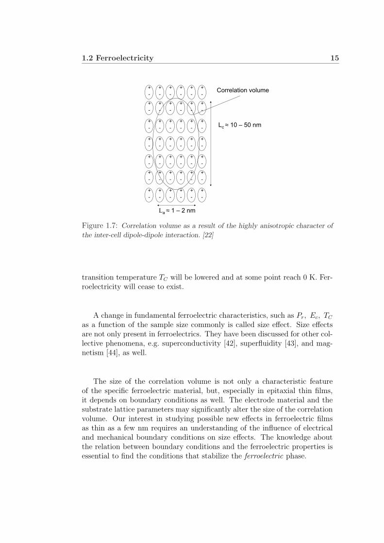
In a simple picture, ferroelectricity can be seen as a collective phenomenon,associated with the alignment of localized dipoles within a correlation vol-ume, producing a spontaneous polarization [40].
Consider a single dipole in vacuum. Any moment applied to it will rotatethe dipole. Therefore, no stable polarization can be based on a free dipole.A number of dipoles, however, will align parallel to the polarization due tothe highly anisotropic character of the inter-cell dipole-dipole interaction. Itis long-range parallel to the polarization axis and short-range perpendicularto the polarization axis. The volume filled up by the number of dipoles,necessary to achieve a stable polarization, is called the correlation volume.In Fig. 1.7 the correlation volume is schematically shown.
Please note that there is a short-range repulsion for the parallel alignmentof two adjacent dipoles perpendicular to the polarization axis and energeti-cally favorable, long-range Coulomb forces for the parallel alignment of twoadjacent dipoles parallel to the polarization axis. Owing to the mentionedanisotropy, the energy gain associated with the parallel alignment of thedipoles is larger than the loss in energy associated with the parallel alignmentof adjacent dipoles perpendicular to the polarization axis [41]. According toLines and Glass [22], typical values for the correlation volume for many fer-roelectrics are given by Lc ∼ 10− 50 nm and La ∼ 1− 2 nm.
The reduction of the thickness of the ferroelectric thin film below LC willthus reduce the stability of the ferroelectric phase. In other words, the phase
1.2 Ferroelectricity 15
+
-
+
-
+
-
+
-
+
-
+
-
+
-
+
-
+
-
+
-
+
-
+
-
+
-
+
-
+
-
+
-
+
-
+
-
+
-
+
-
+
-
+
-
+
-
+
-
+
-
+
-
+
-
+
-
+
-
+
-
+
-
+
-
+
-
+
-
+
-
+
-
+
-
+
-
+
-
+
-
+
-
+
-
Lc
≈ 10 – 50 nm
La
≈ 1 – 2 nm
Correlation volume
Figure 1.7: Correlation volume as a result of the highly anisotropic character of
the inter-cell dipole-dipole interaction. [22]
transition temperature TC will be lowered and at some point reach 0 K. Fer-roelectricity will cease to exist.
A change in fundamental ferroelectric characteristics, such as Pr, Ec, TC
as a function of the sample size commonly is called size effect. Size effectsare not only present in ferroelectrics. They have been discussed for other col-lective phenomena, e.g. superconductivity [42], superfluidity [43], and mag-netism [44], as well.
The size of the correlation volume is not only a characteristic featureof the specific ferroelectric material, but, especially in epitaxial thin films,it depends on boundary conditions as well. The electrode material and thesubstrate lattice parameters may significantly alter the size of the correlationvolume. Our interest in studying possible new effects in ferroelectric filmsas thin as a few nm requires an understanding of the influence of electricaland mechanical boundary conditions on size effects. The knowledge aboutthe relation between boundary conditions and the ferroelectric properties isessential to find the conditions that stabilize the ferroelectric phase.
16 The ferroelectric thickness limit
1.3 Electrical boundary conditions
The fundamental relation between electric displacement ~D, field ~E, and po-larization ~P is given by
~D = ε0~E + ~P . (1.24)
Here, the polarization arises from both the spontaneous parallel alignmentof dipoles ~PS described in Chapter 1.2 and the polarizability of ferroelectricsin the presence of an electric field ~PE = χ~E.
A homogeneous, spontaneous polarization along the z-axis ~PS = (0, 0, PS)
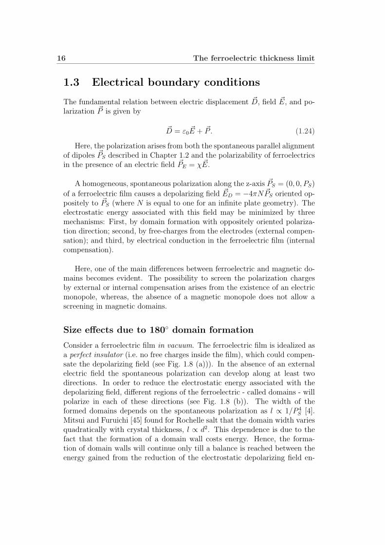
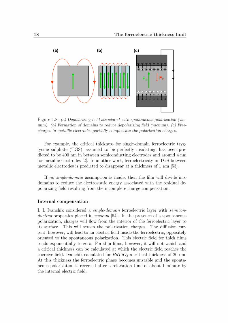
of a ferroelectric film causes a depolarizing field ~ED = −4πN ~PS oriented op-positely to ~PS (where N is equal to one for an infinite plate geometry). Theelectrostatic energy associated with this field may be minimized by threemechanisms: First, by domain formation with oppositely oriented polariza-tion direction; second, by free-charges from the electrodes (external compen-sation); and third, by electrical conduction in the ferroelectric film (internalcompensation).
Here, one of the main differences between ferroelectric and magnetic do-mains becomes evident. The possibility to screen the polarization chargesby external or internal compensation arises from the existence of an electricmonopole, whereas, the absence of a magnetic monopole does not allow ascreening in magnetic domains.
Size effects due to 180 domain formation
Consider a ferroelectric film in vacuum. The ferroelectric film is idealized asa perfect insulator (i.e. no free charges inside the film), which could compen-sate the depolarizing field (see Fig. 1.8 (a))). In the absence of an externalelectric field the spontaneous polarization can develop along at least twodirections. In order to reduce the electrostatic energy associated with thedepolarizing field, different regions of the ferroelectric - called domains - willpolarize in each of these directions (see Fig. 1.8 (b)). The width of theformed domains depends on the spontaneous polarization as l ∝ 1/P 4
S [4].Mitsui and Furuichi [45] found for Rochelle salt that the domain width variesquadratically with crystal thickness, l ∝ d2. This dependence is due to thefact that the formation of a domain wall costs energy. Hence, the forma-tion of domain walls will continue only till a balance is reached between theenergy gained from the reduction of the electrostatic depolarizing field en-
1.3 Electrical boundary conditions 17
ergy and the energy necessary to create the domain walls. In this case thelong-range depolarizing field inside the film becomes negligible, whereas nearthe film surfaces on a length-scale comparable to the domain width a highlyfluctuating depolarizing field is still present [46].
Size effects due to incomplete screening of the depolar-izing field
External compensation
Large depolarizing fields can be avoided not only by the formation of do-mains, but also by the accumulation of compensating charges at the surfacesperpendicular to the polarization. Consider a ferroelectric film sandwichedbetween two metallic electrodes in a short-circuit condition. As it was the casefor the ferroelectric film in vacuum, a homogeneous spontaneous polarizationalong the z-axis of the idealized insulating film gives rise to a depolarizingfield oriented oppositely to its origin, the spontaneous polarization. Otherthan in the vacuum case, the metallic electrodes contain free charges, whichcan compensate for the polarization charges. In this case, the width of thedomains is given by l ∝ 1/(PS + σ) where σ is the surface charge density [4].A monodomain sample is obtained for a complete compensation σ = −PS ofthe polarization.
It is known, however, that short circuited electrodes do not provide anexact cancellation of the depolarizing field. A complete compensation of thepolarization charges cannot be achieved due to the separation of the freecharges in the electrodes and the bounded charges in the ferroelectric (seeFig. 1.8 (c)). The compensation of the polarization depends on the screeninglength of the electrode. The Thomas-Fermi screening length in a metal isapproximately 0.5 − 1 A, whereas the Debye-length in a semiconductor islarger by approximately three orders of magnitude [47].
Batra and Silverman showed that the incomplete compensation of thepolarization charges changes the stability of the ferroelectric phase [2, 48, 49,50, 51, 52, 3]. The depolarizing field that results from an incomplete com-pensation of the polarization charges becomes significant when the thicknessof the ferroelectric film is reduced. It results then in a depression of the spon-taneous polarization and transition temperature. The use of semiconductingelectrodes can even change the nature of the phase transition from second tofirst-order [49].
18 The ferroelectric thickness limit
PS
(a) (b) (c)
ED
Figure 1.8: (a) Depolarizing field associated with spontaneous polarization (vac-
uum). (b) Formation of domains to reduce depolarizing field (vacuum). (c) Free-
charges in metallic electrodes partially compensate the polarization charges.
For example, the critical thickness for single-domain ferroelectric tryg-lycine sulphate (TGS), assumed to be perfectly insulating, has been pre-dicted to be 400 nm in between semiconducting electrodes and around 4 nmfor metallic electrodes [2]. In another work, ferroelectricity in TGS betweenmetallic electrodes is predicted to disappear at a thickness of 1 µm [53].
If no single-domain assumption is made, then the film will divide intodomains to reduce the electrostatic energy associated with the residual de-polarizing field resulting from the incomplete charge compensation.
Internal compensation
I. I. Ivanchik considered a single-domain ferroelectric layer with semicon-ducting properties placed in vacuum [54]. In the presence of a spontaneouspolarization, charges will flow from the interior of the ferroelectric layer toits surface. This will screen the polarization charges. The diffusion cur-rent, however, will lead to an electric field inside the ferroelectric, oppositelyoriented to the spontaneous polarization. This electric field for thick filmstends exponentially to zero. For thin films, however, it will not vanish anda critical thickness can be calculated at which the electric field reaches thecoercive field. Ivanchik calculated for BaTiO3 a critical thickness of 20 nm.At this thickness the ferroelectric phase becomes unstable and the sponta-neous polarization is reversed after a relaxation time of about 1 minute bythe internal electric field.
1.3 Electrical boundary conditions 19
Batra et al. studied the case of internal compensation of the polarizationeither by free carriers in space charge layers, or by charges trapped in surfacestates of the ferroelectric. They found that space charge regions occur at thesurface of a ferroelectric [49, 3]. The reason for this incomplete compensa-tion of polarization is the lack of states at the Fermi level for an only slightlyconducting ferroelectric film.
In conclusion, it is unlikely to achieve a monodomain state for thin filmsif the injection of charge from external electrodes is excluded.
Size effects due to surface effects
Even if the surface charge is fully compensated at the metallic electrodes, afinite size effect can be present. Differences in the remanent polarization andcoercive field for thin films compared to bulk material3 are often theoreticallyaccounted for by introducing subsurface layers, whose electric properties dif-fer from those of the bulk material.
Ions in a subsurface layer have a different number of nearest neighborsfrom those in the bulk, therefore, the local polarization is expected to varyin the vicinity of a surface. A depolarizing field arises from bound chargesinside the ferroelectric. This depolarizing field is different from the one dis-cussed by Batra et al., which was the result of an incomplete compensationof polarization. Here, the depolarizing field is due to spatial variations of thepolarization in the film.
Surface effects are described by an inhomogeneous Landau-Devonshiretheory, which includes a spatial variation of the polarization in the vicinity ofthe surface [55]. In the approach proposed by Kretschmer and Binder [4, 56],the free energy is given by FFilm = Fbulk+Fsurface. They introduce the extrap-olation length λ, which measures the strength of coupling in the subsurfacelayers. The local polarization near the surface is expected to change over adistance comparable to the bulk correlation length ξ of polarization fluctu-ations. Please note that the correlation length ξ is not identical with theparameters of the correlation volume LA and LC introduced in Chapter 1.2.Usually λ is considered to be positive for ferroelectric thin films, which corre-sponds to a polarization suppression in subsurface layers. Scott [57] indicates
3I refer to bulk material as a sample for which the bulk properties are dominant overthe surface properties.
20 The ferroelectric thickness limit
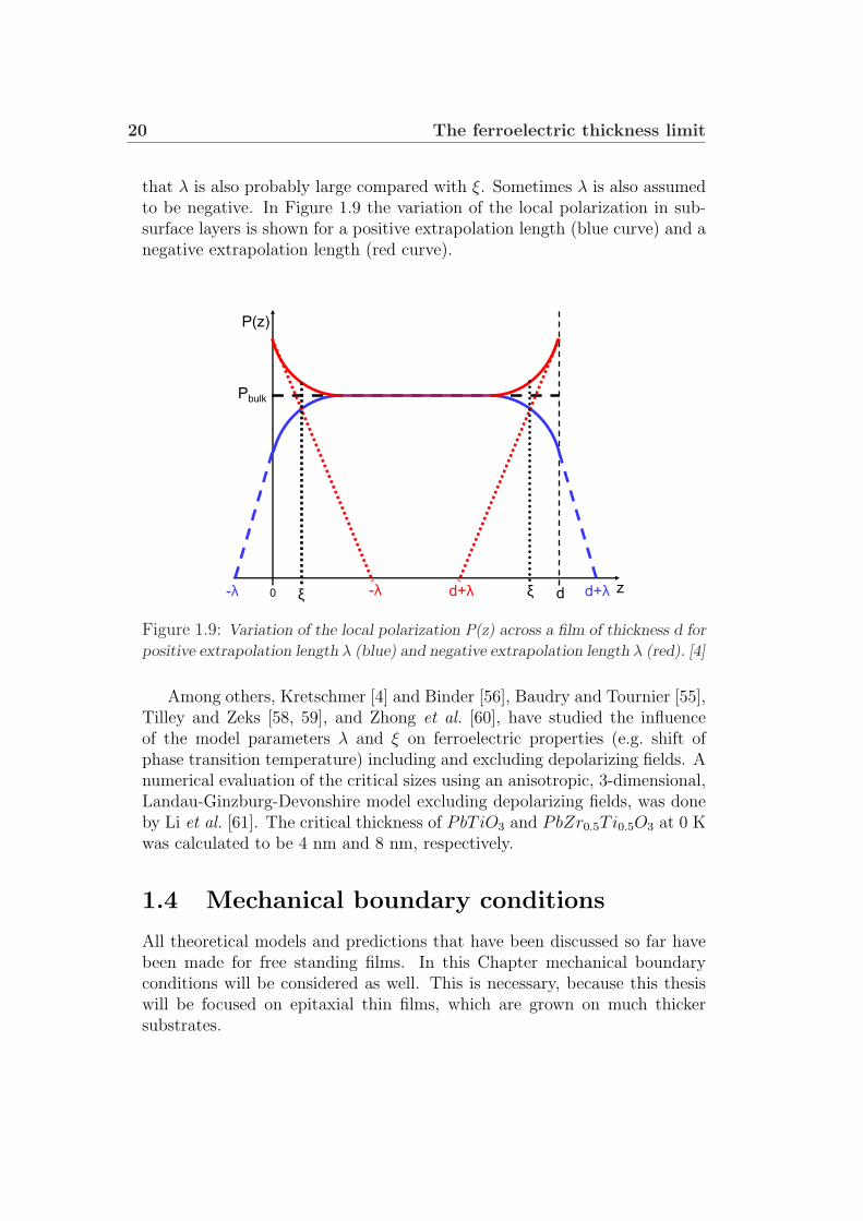
that λ is also probably large compared with ξ. Sometimes λ is also assumedto be negative. In Figure 1.9 the variation of the local polarization in sub-surface layers is shown for a positive extrapolation length (blue curve) and anegative extrapolation length (red curve).
P(z)
z0 d-λ d+λ
Pbulk
-λ d+λξ ξ
Figure 1.9: Variation of the local polarization P(z) across a film of thickness d for
positive extrapolation length λ (blue) and negative extrapolation length λ (red). [4]
Among others, Kretschmer [4] and Binder [56], Baudry and Tournier [55],Tilley and Zeks [58, 59], and Zhong et al. [60], have studied the influenceof the model parameters λ and ξ on ferroelectric properties (e.g. shift ofphase transition temperature) including and excluding depolarizing fields. Anumerical evaluation of the critical sizes using an anisotropic, 3-dimensional,Landau-Ginzburg-Devonshire model excluding depolarizing fields, was doneby Li et al. [61]. The critical thickness of PbT iO3 and PbZr0.5Ti0.5O3 at 0 Kwas calculated to be 4 nm and 8 nm, respectively.
1.4 Mechanical boundary conditions
All theoretical models and predictions that have been discussed so far havebeen made for free standing films. In this Chapter mechanical boundaryconditions will be considered as well. This is necessary, because this thesiswill be focused on epitaxial thin films, which are grown on much thickersubstrates.
1.4 Mechanical boundary conditions 21
Extrinsic size effects of mechanical origin
The interaction of the film with the substrate can generate significant me-chanical stresses in the film. Growth stresses may appear during the filmdeposition in the paraelectric phase. These stresses strongly depend on pa-rameters of the deposition process [62]. Energetic deposition techniques, suchas rf sputtering (see p. 59) or pulsed laser deposition (see p. 56), favor com-pressive growth stresses, whereas tensile growth stresses result from rapid lowenergy growth techniques, such as molecular oxide chemical vapor depositionor thermal evaporation (see p. 57) [63]. It has been shown that during thegrowth (usually in the paraelectric state) of thicker films, substantial stressrelaxation is favored by the generation of arrays of misfit dislocations at thefilm/substrate interface [63], whereas thinner films grow in their coherentpseudomorphic cubic phase retaining their epitaxial strain [64].
During cooling from the growth temperature, thermal stresses may arisein the film due to differences between the mean coefficients of thermal ex-pansion of substrate and film.
The paraelectric-ferroelectric phase transition, producing dimensionalchanges, introduces additional stresses leading to the formation of domains(elastic stress relaxation) and sometimes to additional formation of misfitdislocations [63].
Strain induced by the substrate may lead to lattice parameters in epitaxialthin films that differ considerably from those in bulk material. A misfit-strainSm independent of the film polarization state is introduced into the theoryto describe substrate effects on the spontaneous polarization. For perovskitefilms grown on cubic substrates, this strain may be defined as Sm = (b−a0)/b,where b is the substrate lattice parameter and a0 is the equivalent cubic cellconstant of a free standing film [65]. This definition of Sm is only valid forfully strained films. Above a critical film thickness, misfit dislocations areintroduced into the film and a substrate effective lattice parameter b∗ insteadof the actual lattice constant b has to be used [63]:
Sm =b∗ − a0
b∗. (1.25)
Note that the strain is always given with respect to the paraelectric state.The polarization is coupled to the lattice strain due to electrostriction (seepage 4). Therefore, according to thermodynamic calculations by Pertsev
et al., the magnitude and orientation of the spontaneous polarization ~PS
22 The ferroelectric thickness limit
strongly depend on the value of Sm [5, 66]. A ferroelectric thin film, suchas BaTiO3 or Pb(Zr, T i)O3, grown on a tensile substrate Sm > 0 tends toform a ferroelectric phase with an in-plane polarization direction, whereasits growth on a compressive substrate Sm < 0 will stabilize the ferroelec-tric phase with an out-of-plane orientation and enhance the spontaneouspolarization in this direction. Remarkably, in agreement with experimentalresults [8] the spontaneous polarization PS(Sm < 0) can be larger than thebulk polarization. Higher values of PS can be obtained by increasing themagnitude of compressive strain in the film. This, however, will decrease thecritical thickness at which misfit dislocations are introduced.
In conclusion of this Section, the size effect of mechanical origin is at-tributed to the thickness dependence of the film in-plane lattice strain Sm.For a given thickness of the ferroelectric thin film, the highest compressivestrain, which is achievable without leading to misfit dislocations, will beststabilize the ferroelectric against the paraelectric phase.
Intrinsic size effects in strained epitaxial films
As discussed in Chapter 1.3 on page 19, Kretschmer and Binder added asurface term to the Landau expansion of the total free energy (eqn. (1.4))and introduced the extrapolation length λ into the thermodynamic theory inorder to describe surface effects. The expansion of the free energy, proposedby Kretschmer and Binder in the notation of Tilley and Zeks [59], for a filmof thickness d is given by
FA
=∫ d
0
[12BP 2 + 1
4CP 4 + 1
2E ( dP
dz)2
]dz + 1
2λE(P 2
− + P 2+).
Here, A is the surface area of the film. P− = P (0), P+ = P (d) and λ isthe extrapolation length. The last term is the added surface term. Later,the free energy was expanded to powers of the order parameter P of upto the sixth [67] in order to describe ferroelectric materials that undergo afirst-order phase transition (see Chapter 1.2)
F
A=
∫ d
0
[12BP 2 +
14CP 4 +
16DP 6 +
12E
(dP
dz
)2]
dz +12λ
E(P 2−+P 2
+). (1.26)
As mentioned above, Pertsev et al. studied the influence of substrateeffects on the ferroelectric phase state using a thermodynamic theory. Thetwo-dimensional clamping and straining of a ferroelectric film by a dissimilarthick substrate was found to affect considerably its phase state, shifting thetemperature of the ferroelectric transition and changing its order [5, 66].
1.4 Mechanical boundary conditions 23
Zembilgotov et al. developed a phenomenological theory, which describesintrinsic surface effects on the polarization properties of films grown epitaxi-ally on much thicker substrates [6]. This theory considers both surface effectsdiscussed on page 19 and substrate effects discussed on page 22. Zembilgo-tov et al. considered epitaxial thin films of perovskite ferroelectrics grownin a high-temperature paraelectric state on a thick (001)-oriented compres-sive (Sm < 0) cubic substrate and sandwiched between extended identicalelectrodes. Films with a positive extrapolation length, corresponding to apolarization reduction in subsurface layers, were studied. Assuming thatthe polarization changes only along the film thickness direction and ignoringthe depolarizing field, the Helmholtz free energy per unit area (eqn. (1.26))modifies to
F
A=
∫ d
0
F (z)dz +1
2λg11(P
2− + P 2
+), (1.27)
F (z) =S2
m
s11 + s12
+ a∗3(Sm)P 2 + a∗33P4 + a111P
6 +1
2g11
( dP
dz
)2
, (1.28)
a∗3 = a1 − Sm2Q12
s11 + s12
, a∗33 = a11 +Q2
12
s11 + s12
. (1.29)
Here, a1, a11 and a111 are the dielectric stiffness and higher-order stiff-ness coefficients at constant stress; Qij are the electrostrictive constants; sij
are the elastic compliances at constant polarization; λ is the extrapolationlength; z is the out-of-plane direction; P is the out-of-plane polarization andP−,; and P+ are the polarization values on the film surfaces, i.e. at z = 0and z = d, respectively. The dielectric stiffness constant a1 is assumed to bea linear function of temperature near the Curie-Weiss temperature (Curie-Weiss-law: a1 = (T − T0)/2ε0C). All other coefficients are assumed to beindependent of temperature. Using this thermodynamic approach it is possi-ble to calculate the mean polarization P as a function of the film thickness d,temperature T , and misfit-strain Sm in the epitaxially grown heterostructure.
The intrinsic size effect on the polarization in strained films was shownto be governed by the normalized film thickness d/ξ∗ and the ratio λ/ξ∗.Here, ξ∗ =
√g11/|a∗3| is the modified correlation length, which differs from
the bulk correlation length ξ =√
g11/|a1| of a mechanically free bulk crystal.The correlation length ξ∗0(Sm = 0) = ξ(T = 0) was found to be about 1 nmfor PbT iO3 and 5 nm for BaTiO3 [6].

24 The ferroelectric thickness limit
The variation of the film mean polarization P , with temperature T shownin Fig. 1.10 (a) for PbT iO3 and in Fig. 1.10 (b) for BaTiO3, results mainlyfrom the temperature dependence of the dielectric stiffness a1. The surfaceeffect hinders the development of spontaneous polarization during the filmcooling. This intrinsic size effect is considerable only for ultrathin films andmanifests itself in a decrease of the ferroelectric transition temperature TC ,as well as in a reduction of the mean polarization P (T ) relative to the thickfilm polarization.
(a) (b)
-200 -100 0 100 200 300 400 5000.0
0.2
0.4
0.6
0.8
1.0
10521
Temperature, °C
|
PbTiO3
Mean p
ola
rization, P
/Ps
0
-50 0 50 100 150 200 2500.0
0.2
0.4
0.6
0.8
1.0
2 5 10 20
BaTiO3
|
Mean p
ola
rization, P
/Ps
0
Temperature, °C
Figure 1.10: Normalized mean polarization P (T )/P T=0bulk of epitaxial (a) PbT iO3
grown at Sm = 0 and (b) BaTiO3 grown at Sm = −4.6×10⁻³ as a function of the
temperature T . Numbers indicate the normalized film thickness d/ξ∗0 . ξ∗0(Sm = 0)coincides with the bulk correlation length ξ0(T = 0). [6]
The transition temperature for ultrathin epitaxial films is governed bythe competition of substrate and surface effects on TC (see Fig. 1.11 (a) forPbT iO3 thin films). On the one hand, the transition temperature TC shiftsto higher values at negative misfit strains provided by a compressive sub-strate, on the other hand, the negative surface effect (λ > 0) tends to reduceTC . Note that for thicker films surface effects can be neglected. A significantsuppression of the transition temperature is expected to occur only at smallmisfit strains and a thickness of about 2ξ0 and below.
Finally, the mean polarization P has been calculated at room temperatureas a function of the misfit-strain Sm (see Fig. 1.11 (b) for BaTiO3 thin films).
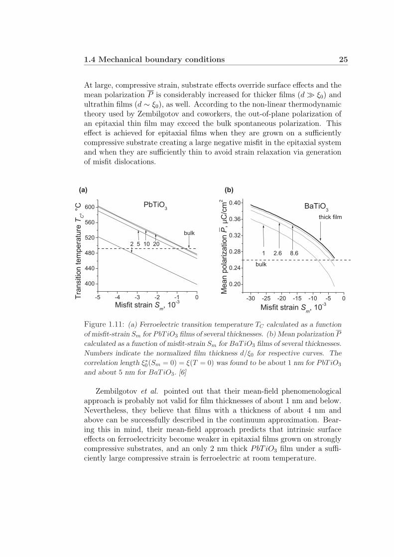
1.4 Mechanical boundary conditions 25
At large, compressive strain, substrate effects override surface effects and themean polarization P is considerably increased for thicker films (d À ξ0) andultrathin films (d ∼ ξ0), as well. According to the non-linear thermodynamictheory used by Zembilgotov and coworkers, the out-of-plane polarization ofan epitaxial thin film may exceed the bulk spontaneous polarization. Thiseffect is achieved for epitaxial films when they are grown on a sufficientlycompressive substrate creating a large negative misfit in the epitaxial systemand when they are sufficiently thin to avoid strain relaxation via generationof misfit dislocations.
-30 -25 -20 -15 -10 -5 0
0.20
0.24
0.28
0.32
0.36
0.40
thick film
|
bulk
1 2.6 8.6
BaTiO3
Mean p
ola
rization P
,µC
/cm
2
Misfit strain Sm, 10
-3
-5 -4 -3 -2 -1 0
400
440
480
520
560
600
bulk
2 5 10 20
PbTiO3
Tra
nsitio
n tem
pera
ture
TC, °C
Misfit strain Sm, 10
-3
(a) (b)
Figure 1.11: (a) Ferroelectric transition temperature TC calculated as a function
of misfit-strain Sm for PbT iO3 films of several thicknesses. (b) Mean polarization P
calculated as a function of misfit-strain Sm for BaTiO3 films of several thicknesses.
Numbers indicate the normalized film thickness d/ξ0 for respective curves. The
correlation length ξ∗0(Sm = 0) = ξ(T = 0) was found to be about 1 nm for PbT iO3
and about 5 nm for BaTiO3. [6]
Zembilgotov et al. pointed out that their mean-field phenomenologicalapproach is probably not valid for film thicknesses of about 1 nm and below.Nevertheless, they believe that films with a thickness of about 4 nm andabove can be successfully described in the continuum approximation. Bear-ing this in mind, their mean-field approach predicts that intrinsic surfaceeffects on ferroelectricity become weaker in epitaxial films grown on stronglycompressive substrates, and an only 2 nm thick PbT iO3 film under a suffi-ciently large compressive strain is ferroelectric at room temperature.
26 The ferroelectric thickness limit
Recently, a further expansion of the total free energy has been sug-gested [68], accounting for the electric field inside the ferroelectric, the energyassociated to the formation of domain walls in polydomain films, and spatialinhomogeneities of the polarization inside the film:
Ffilm = Fbulk +Fsurface +Fstrain +Felectric field + Fdomain wall + Fgradient. (1.30)
The existence of ferroelectricity in ultrathin films is further theoreticallysupported by ab-initio calculations [69, 70]. Using an effective Hamiltonian,Ghosez and Rabe predicted a stable ferroelectric phase in a free-standingPbT iO3 film as thin as a few unit cells [7, 69].
The predicted minimum thickness for ferroelectricity has decreased overtime significantly. Early works from Batra and Silverman predicted a min-imum thickness of 400 nm. Nowadays, theoretical studies predict ferroelec-tricity in ultrathin films with only a few monolayers. This substantial changeof the predictions over time is mainly due to a better understanding of the in-fluence of electrical and mechanical boundary conditions. On the other hand,not only the predictions are more accurate nowadays. Especially in the last5 years a lot of experimental work has been done and the outcome of the im-proved deposition and analytical techniques has been quite considerable. Tenyears ago the thickness dependence of the remanent polarization was usuallyshown on a micrometer-scale [36]. Nowadays this dependence is plotted on ananometer scale. Yanase et al. showed nicely shaped P-E curves for 12 nmthick BaTiO3 films [8]. Based on their AFM-investigations, Tybell et al. re-ported on the existence of ferroelectricity in 4 nm thick PbT iO3 [9]. Recently,Streiffer et al. found 180 stripe domains in 3 monolayers of PbT iO3 [11, 10]by in-situ grazing-incidence x-ray scattering and followed the existence offerroelectricity in this only 1.2 nm thick film.
In conclusion, under suitable boundary conditions ferroelectricity is likelyto survive in films as thin as a few nm. The pursuit for the ferroelectricminimum in thickness has reached a thickness range where electron tunnelingthrough these films may be expected.
Chapter 2
Quantum-mechanical tunneling
Electron tunneling through a thin insulating layer or vacuum in between twoelectrodes has been studied for 80 years. The observation of the tunneling ef-fect supported the wave - particle dualism and, therefore, played a significantrole in the development of quantum mechanics during the twenties [71, 72].
In this Chapter the tunneling through a metal-insulator-metal contactwill be described as a quantum-mechanical effect. It will be shown thatfor a sufficiently thin insulating barrier, a current flow through this barrieris possible as a result of an overlap of the wave functions of the electronsin both metals. Elastic and inelastic tunneling will be introduced and thetemperature and voltage dependencies of these conduction mechanisms willbe discussed.
2.1 Tunneling effect
Consider two metals, M1 and M2, separated by a thin insulating barrierwith thickness d. In a simple model the barrier can be described by a one-dimensional, symmetric square potential of height V0 and width d. Thismodel only holds for a system for which the barrier heights Φ1 and Φ2 at bothmetal-insulator interfaces are the same. For tunnel junctions with differentelectrodes, however, different barrier heights have to be assumed resulting, ina simplified model, in a trapezoidal potential barrier [73]. In Fig. 2.1, a tun-nel junction is shown schematically, consisting of a thin insulating layer withthickness d in between two metal layers, M1 and M2. At 0 K the electrons,which exist in M1 and M2 in pairs in discrete energy levels, fill up the well tothe Fermi levels EF1 and EF2, respectively. The work functions of the metalsW1 and W2 represent the minimum energy required to free electrons from the
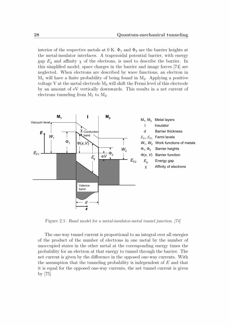
28 Quantum-mechanical tunneling
interior of the respective metals at 0 K. Φ1 and Φ2 are the barrier heights atthe metal-insulator interfaces. A trapezoidal potential barrier, with energygap Eg and affinity χ of the electrons, is used to describe the barrier. Inthis simplified model, space charges in the barrier and image forces [74] areneglected. When electrons are described by wave functions, an electron inM1 will have a finite probability of being found in M2. Applying a positivevoltage V at the metal electrode M2 will shift the Fermi level of this electrodeby an amount of eV vertically downwards. This results in a net current ofelectrons tunneling from M1 to M2.
Φ1
W1
W2Φ2eV
E
ΕgEF2
EF1
Φ(x,V)
x
d
χ
Valence
band
Conduction
band
M1
M2I
Vacuum levelM1, M2 Metal layers
I Insulator
d Barrier thickness
EF1, EF2 Fermi levels
W1, W2 Work functions of metals
Φ1, Φ2 Barrier heights
Φ(x, V) Barrier function
Eg Energy gap
χ Affinity of electrons
Figure 2.1: Band model for a metal-insulator-metal tunnel junction. [74]
The one-way tunnel current is proportional to an integral over all energiesof the product of the number of electrons in one metal by the number ofunoccupied states in the other metal at the corresponding energy times theprobability for an electron at that energy to tunnel through the barrier. Thenet current is given by the difference in the opposed one-way currents. Withthe assumption that the tunneling probability is independent of E and thatit is equal for the opposed one-way currents, the net tunnel current is givenby [75]
2.1 Tunneling effect 29
I(V ) = const×∫
ρ2(E− eV ) ρ1(E) [f(E− eV )−f(E)] |M(E)|2 dE. (2.1)
Here, ρ1 and ρ2 are the densities-of-states functions for M1 and M2, re-spectively. f(E) is the Fermi distribution function and M(E) is the transfermatrix element for the electrons of energy E from one side of the barrier tothe other one. In the WKB approximation [76], which implies that the bandstructure of the metal-insulator-metal system varies only slowly compared tothe electron wavelength, the tunneling probability is given by [77]
|M(E)|2 = exp ( −2
∫ d
0
[ −k2x]
1/2dx ), (2.2)
where x and kx are the coordinate and the electron wave number, respec-tively, normal to the film plane. The parabolic energy-momentum relationmay be written as
p2x
2m∗ =~2k2
x
2m∗ = Ex − Φ(x, V ), (2.3)
where Φ(x, V ) is the barrier function and Ex is the energy of electronsin the barrier with the effective mass m∗. For Ex > Φ(x), the electronwave number is real, meaning that the electron wave function is periodic(Ψ ∼ e±ikxx). On the other hand, for the electrons tunneling through thebarrier (Ex < Φ(x)), the electron wave number is imaginary and the electronwave function decays exponentially (Ψ ∼ e±kxx) inside the barrier.
Using eqn. (2.3) the tunneling probability modifies to
|M(E)|2 = c · exp(−4π
h
∫ d
0
√2m∗ ( Φ(x, V )− Ex ) dx
). (2.4)
In order to simplify the calculations, Simmons [78] replaced the barrierΦ(x) by an average barrier Φ = (Φ1 + Φ2)/2. However, by applying thisapproximation of an average barrier height, all information about barrierasymmetry is lost. Therefore, Brinkman introduced the parameter ∆Φ =Φ2−Φ1 to account for an asymmetrical barrier [79]. He pointed out that evenusing the same metal material for top and bottom electrodes, different growthconditions at the metal/insulator and insulator/metal interfaces could leadto an asymmetry in the barrier. According to Brinkman, the tunnel currentdensity for Φ À eV , d > 10 A, ∆Φ/Φ < 1 is given approximately by
30 Quantum-mechanical tunneling
I(V )A
∼= 3.16 · 1010
√Φd
exp( −1.025 d
√Φ
)[
V − 0.0213d ·∆ΦΦ3/2
V 2 + 0.0109d2
ΦV 3
].
(2.5)Here, the current density is given in A/cm2, the barrier height in eV and
the barrier thickness in A.
2.2 Elastic and inelastic electron tunneling
The theories that will be introduced in this Chapter were developed to de-scribe the different electron tunneling conduction mechanisms through amor-phous barriers, e.g. amorphous silicon. Amorphous silicon is characterizedby a large number of localized states in its forbidden band. The existenceof those localized states, characteristic of non-crystalline materials, is crucialfor the electron transport in amorphous materials. It is believed that thepresence of a relatively high density of local defects in perovskite materi-als may allow the use of those theories for these crystalline grown materialsas well [80, 81]. Local defects with an attractive potential act as localizedstates. Only the existence, not the origin of these localized states near theFermi surface, is important for electron tunneling. In fact, Mott’s T−1/4 law(see p. 34) has been successfully used to identify variable range hopping asthe dominant conduction mechanism in crystalline SrT iO3 at temperaturesabove 130 K [80]. Direct tunneling and tunneling via N localized states havebeen found to fit experimental data for SrT iO3 tunnel junctions [82, 83] andfor SrT iO3 bicrystal junctions [84], although doubts about the applicabilityof those theories were pointed out by the author himself.
Direct tunneling
The incident electron wave function decays inside the barrier exponentiallyover a distance known as the localization length α−1. For a barrier thicknessd, not much thicker than the localization length, direct tunneling from oneelectrode to the other is observed (see Fig. 2.2). It is known that the local-ization length for an amorphous silicon barrier is α−1 ≈ 7 A. For epitaxialSrT iO3, the localization length was found to be ≈ 4 A [82, 83].
For small voltages the direct tunneling conductance is simply [85]:
Gdir0 = Gdir
0 · exp ( −2αd ) . (2.6)
2.2 Elastic and inelastic electron tunneling 31
There is only a weak temperature dependence of the direct tunnelingconductance [86] due to thermal broadening of the Fermi surface at finitetemperatures [87]. However, as the barrier thickness increases transport vialocalized states (elastic and inelastic) becomes dominant.
∆ε = kBT
ω
M1 M2I
(a)
(b)
(c)
Figure 2.2: Sketch showing (a) direct tunneling, (b) resonant tunneling and (c)
tunneling via two localized states
Resonant tunneling
An elastic electron transport via a localized state is referred to as resonanttunneling. Unlike direct tunneling, where electrons from one electrode aretransferred to the other as a result of an overlap of the electron wave func-tions in both electrodes, here the barrier thickness is much thicker than thelocalization length and the transfer is composed by two single tunnel events.An electron tunnels from the left electrode to a localized state, then fromthis localized state to the right electrode (see Fig. 2.2). It has been shownthat only localized states, situated at (d+α−1)/2 and within an energy widthEF ± Γ
2, are likely to contribute to the resonant tunneling conductance [85].
Here, Γ is referred to as the intrinsic width of the states. The total resonanttunneling conductance is given by the sum over the contributions from eachresonant channel within the junction area A. In a simplified notation, theresonant tunneling conductance is given by
Gres1 = Gres
1 · exp ( −αd ) . (2.7)
32 Quantum-mechanical tunneling
It can be easily seen from equations (2.6, 2.7) that for a sufficiently largebarrier thickness d the resonant tunneling conductance becomes dominantover the direct tunneling conductance G1 > G0.
There are also theoretical studies [88, 89] claiming that resonant tunnel-ing through two or more localized states should exist and predominate inthe limit of very thick barriers at extremely low temperatures. The largercontribution to the conductance by phonon-assisted, inelastic hopping pro-cesses described in the following Section, however, prevent them from beingexperimentally observed.
Resonant tunneling is usually temperature-independent. As for directtunneling, there is only a weak quadratic temperature dependence resultingfrom a smearing of the Fermi energy at finite temperatures. Glazman andShekter [90], however, showed that an electron-phonon interaction will leadto an elastic and inelastic resonant tunneling part. The inelastic resonanteffects will introduce a weak temperature-dependent correction to the reso-nant tunneling conduction.
It is generally believed that inelastic effects, resulting from electrons in-teracting with lattice phonons and phonon-assisted electron hopping destroythe phase coherence, which is essential to the resonance, and thereby reducetheir relative significance.
Inelastic hopping via two or more localized states
In their phenomenological theory, Stone and Lee [91] proposed that vari-able range hopping (p. 34) is the main inelastic conduction mechanism thatcompetes with resonant tunneling. They obtained their results treating theinelastic processes from a scattering point of view. No microscopic model ofelectron phonon interaction was assumed.
The dynamics of the tunneling process was first treated quantum me-chanically by Glazman and Matveev [92]. They investigated in detail theprocess of inelastic tunneling through two localized states. Each of these isassumed to couple elastically only to the nearer electrode, whereas the cou-pling between them is assumed to be inelastic, via interaction (emission orabsorption) with phonons (Fig. 2.2).
Electron-phonon interaction causes hopping between two localized states.This is especially important for the states with an energy separation of the

2.2 Elastic and inelastic electron tunneling 33
order of kBT , since when kBT À Γ the elastic coupling between those statesis negligible.
In the low bias-voltage limit, eV ¿ kBT , the studies by Glazman andMatveev predicted
Ghop2 ∝ T (4/3) · exp
( −2αd
3
). (2.8)
Three different factors result in this specific power law. First, a first-orderexpansion made in the small parameter eV/kBT contributes T−1. Second, theintegration over a linear phonon dispersion (appropriate for low-energy acous-tic phonons) combined with the typical energy scale to which the phononshave to couple in order to give rise to the hopping, together contribute T 1/3.And finally, a T 2 contribution is obtained from the requirements that thefirst localized state is within ∼ kBT of the Fermi level, so that electrons areavailable to tunnel onto it, and that the second state is within ∼ kBT of thefirst, so that phonons are available to couple to them [85].
In the high bias-voltage and low temperature limit eV À kBT , a similarpower law is obtained
Ghop2 ∝ V (4/3) · exp
( −2αd
3
). (2.9)
The conduction, due to inelastic hopping along optimal chains, is expo-nentially larger than that of the resonant tunneling in the barrier thickness.This more than compensates for the small probability of realizing such con-figurations.
As the temperature is further increased and as the barriers become thicker,the energy window for hopping increases, and hopping chains with largernumbers of localized states optimally located, though even rarer, may dom-inate the conduction process.
The equations (2.8, 2.9) for hopping via two localized states can be gen-eralized to give the average hopping conductance of the chains consisting ofN localized states.
Low bias-voltage limit: eV ¿ kBT ,
GhopN ∝ TN−[2/(N+1)] · exp
( −2αd
N + 1
). (2.10)

34 Quantum-mechanical tunneling
High bias-voltage and low temperature limit: eV À kBT ,
GhopN ∝ V N−[2/(N+1)] · exp
( −2αd
N + 1
). (2.11)
Variable range hopping
In the bulk limit, d À lV RH , variable range hopping is the dominant con-ductance mechanism. Mott realized that the typical length of a hop, thevariable hopping length lV RH , had to be short enough so as to have a finiteoverlap of the electron wave functions on the two localized states involved.On the other hand, it had to be long enough to find a state with a compara-ble Fermi energy [93]. Mott predicted that the length of a hop increases withdecreasing temperature as T−1/4. The conductance, which is proportional tothe probability of such a hop, is thus, given by
GV RH = GV RH0 · exp
(−
( T
T
)1/4), (2.12)
where T is a characteristic temperature.
Shklovskii proposed an analogous current-field relation for hopping in thelimit of high fields [94]. He predicted that at sufficiently low temperatures(eV À kBT ) the current-field characteristic should be given by
JV RH = JV RH0 · exp
(−
( E
E
)1/4), (2.13)
where the current density J(E) is assumed to be homogeneous and E isa characteristic field.
In summary, the total conductance at any temperature is the sum of thecontribution of elastic and inelastic processes:
G∑(T ) = Gdir0 + Gres
1 +∑N=2
GhopN (T ) + GV RH(T ). (2.14)
Chapter 3
Concept of a FerroelectricTunnel Junction
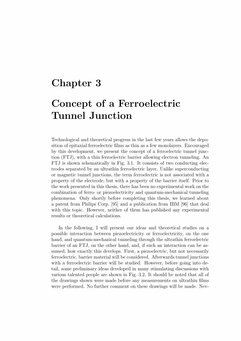
Technological and theoretical progress in the last few years allows the depo-sition of epitaxial ferroelectric films as thin as a few monolayers. Encouragedby this development, we present the concept of a ferroelectric tunnel junc-tion (FTJ), with a thin ferroelectric barrier allowing electron tunneling. AnFTJ is shown schematically in Fig. 3.1. It consists of two conducting elec-trodes separated by an ultrathin ferroelectric layer. Unlike superconductingor magnetic tunnel junctions, the term ferroelectric is not associated with aproperty of the electrode, but with a property of the barrier itself. Prior tothe work presented in this thesis, there has been no experimental work on thecombination of ferro- or piezoelectricity and quantum-mechanical tunnelingphenomena. Only shortly before completing this thesis, we learned abouta patent from Philips Corp. [95] and a publication from IBM [96] that dealwith this topic. However, neither of them has published any experimentalresults or theoretical calculations.
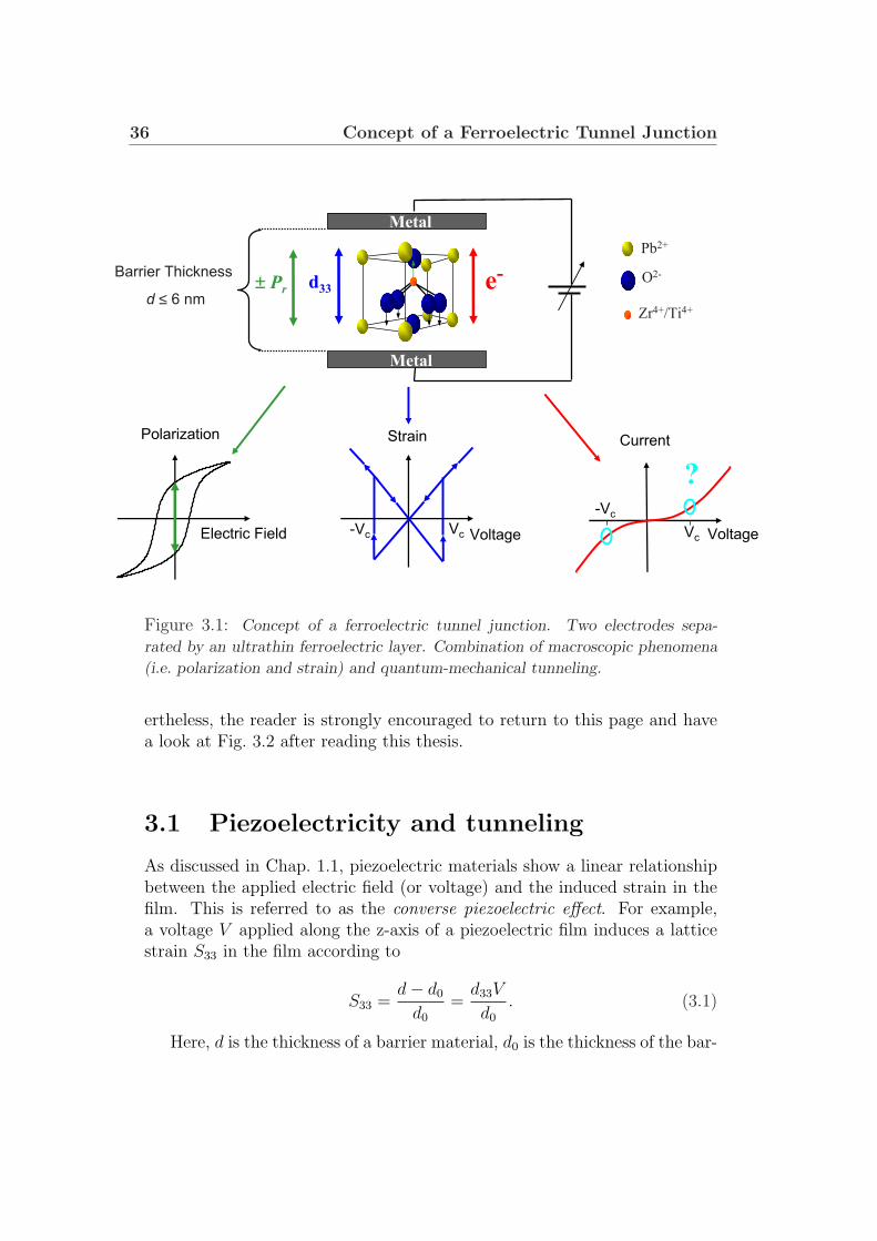
In the following, I will present our ideas and theoretical studies on apossible interaction between piezoelectricity or ferroelectricity, on the onehand, and quantum-mechanical tunneling through the ultrathin ferroelectricbarrier of an FTJ, on the other hand, and, if such an interaction can be as-sumed, how exactly this develops. First, a piezoelectric, but not necessarilyferroelectric, barrier material will be considered. Afterwards tunnel junctionswith a ferroelectric barrier will be studied. However, before going into de-tail, some preliminary ideas developed in many stimulating discussions withvarious talented people are shown in Fig. 3.2. It should be noted that all ofthe drawings shown were made before any measurements on ultrathin filmswere performed. No further comment on these drawings will be made. Nev-
36 Concept of a Ferroelectric Tunnel Junction
Strain
VoltageVc-Vc Voltage
Current
Vc
-Vc
?
Polarization
Electric Field
e-
Metal
Metal
± Pr
Pb2+
O2-
Zr4+/Ti4+
Barrier Thickness
d ≤ 6 nmd33
Figure 3.1: Concept of a ferroelectric tunnel junction. Two electrodes sepa-
rated by an ultrathin ferroelectric layer. Combination of macroscopic phenomena
(i.e. polarization and strain) and quantum-mechanical tunneling.
ertheless, the reader is strongly encouraged to return to this page and havea look at Fig. 3.2 after reading this thesis.
3.1 Piezoelectricity and tunneling
As discussed in Chap. 1.1, piezoelectric materials show a linear relationshipbetween the applied electric field (or voltage) and the induced strain in thefilm. This is referred to as the converse piezoelectric effect. For example,a voltage V applied along the z-axis of a piezoelectric film induces a latticestrain S33 in the film according to
S33 =d− d0
d0
=d33V
d0
. (3.1)
Here, d is the thickness of a barrier material, d0 is the thickness of the bar-
3.1 Piezoelectricity and tunneling 37
(a)(b)
(c)
(d)
Figure 3.2: Results of discussions about the interplay of ferro- or piezoelectric-
ity and quantum-mechanical tunneling with (a) U. Poppe, (b) N. A. Pertsev,
(c) Ch. Buchal, and (d) H. Kohlstedt.
rier in the absence of an applied field and d33 is the longitudinal componentof the piezoelectric third-rank tensor dijk in matrix notation (see Fig. 1.1 (a)).
In the following, various effects of lattice strain on the barrier properties,identified in collaboration with N. A. Pertsev, will be discussed. There aremainly three effects that arise from a change of strain in a piezoelectric film:first, the barrier thickness changes; second, the effective mass of electrons inthe barrier changes due to a change of the lattice parameters; and third, theconduction and the valence band edges shift.
Change in barrier thickness
The most obvious consequence of the converse piezoelectric effect (i.e. thelinear voltage dependence of the strain in the material) is the contraction orexpansion of a piezoelectric material when a voltage is applied to it. Thestrain-free thickness of the piezoelectric material increases by the piezoelec-tric coefficient d33 times the applied voltage V . Consider a piezoelectric filmwith a strain-free thickness in the z-direction equal to d0. If a voltage isapplied along the z-axis, the thickness d is given by
38 Concept of a Ferroelectric Tunnel Junction
d = d0 + d33V. (3.2)
Note that a voltage- or field-induced change in the thickness of the piezo-electric barrier implies an increase or decrease of the distance between theelectrodes of a tunnel junction. This is particularly important due to theexponential dependence of conductance on the barrier thickness, which is aspecific feature of tunneling.
Change of effective mass
Strain increases or decreases the thickness of the piezoelectric barrier. Thechange in the barrier thickness involves a change in the lattice parameters ofthe barrier, as the number of atoms inside the barrier does not change. Usingthe Tight-Binding method [97] proposed by Bloch, which is appropriate ifelectrons are ”tightly bound” to the nuclei of the atoms or, in other words,when the distance between neighboring atoms, a, is large in comparison tothe size of the atoms, the following relation between the effective mass m∗
and the energy width of the conduction band ∆EC (eqn. (5.20) in Ref. [47])is obtained:
m∗ =2 ~
a2 ·∆EC
. (3.3)
Using the exponential dependence of the energy width of the conductionband on the distance between neighboring atoms [47],
∆EC ∼ exp(− a
rα
), (3.4)
where rα ¿ a is a positive constant, gives
m∗ ∼ exp( a
rα
). (3.5)
Considering the strain-induced change of the lattice parameters, a =a0 + a0S33 (see eqn. (3.1)), the partial derivative of the effective mass withrespect to the strain is given by
∂m∗
∂S33
∼ exp( a0
rα
)· a0
rα
, (3.6)
∼ exp( a0
rα
)> 0 .
Consequently, the effective mass of electrons inside a piezoelectric filmcan be written as
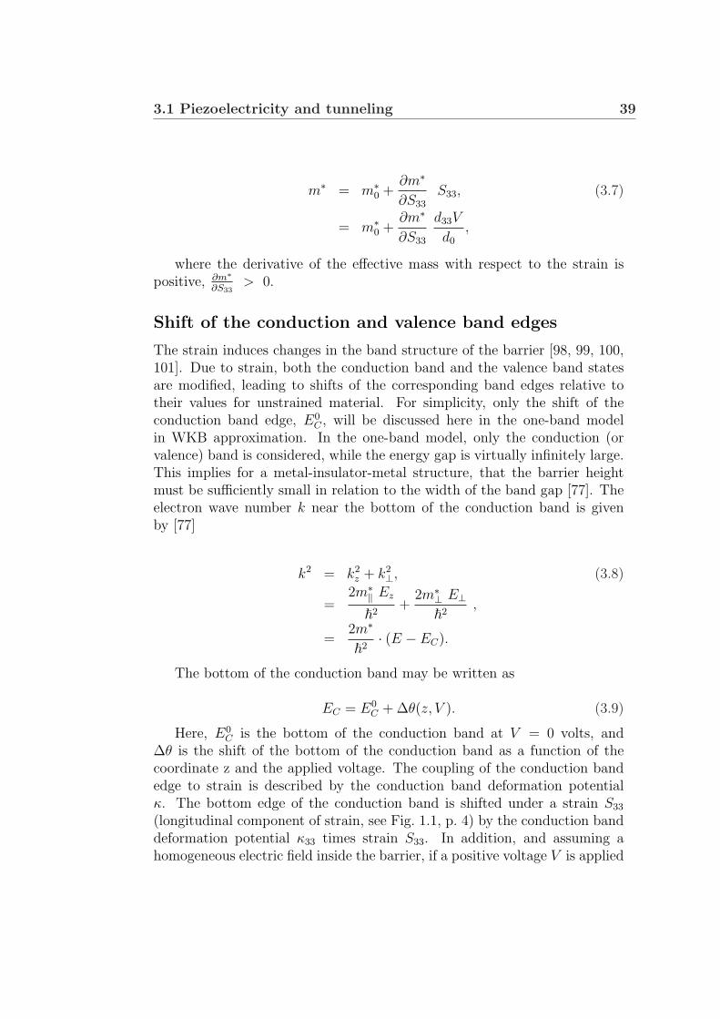
3.1 Piezoelectricity and tunneling 39
m∗ = m∗0 +
∂m∗
∂S33
S33, (3.7)
= m∗0 +
∂m∗
∂S33
d33V
d0
,
where the derivative of the effective mass with respect to the strain ispositive, ∂m∗
∂S33> 0.
Shift of the conduction and valence band edges
The strain induces changes in the band structure of the barrier [98, 99, 100,101]. Due to strain, both the conduction band and the valence band statesare modified, leading to shifts of the corresponding band edges relative totheir values for unstrained material. For simplicity, only the shift of theconduction band edge, E0
C , will be discussed here in the one-band modelin WKB approximation. In the one-band model, only the conduction (orvalence) band is considered, while the energy gap is virtually infinitely large.This implies for a metal-insulator-metal structure, that the barrier heightmust be sufficiently small in relation to the width of the band gap [77]. Theelectron wave number k near the bottom of the conduction band is givenby [77]
k2 = k2z + k2
⊥, (3.8)
=2m∗
‖ Ez
~2+
2m∗⊥ E⊥~2
,
=2m∗
~2· (E − EC).
The bottom of the conduction band may be written as
EC = E0C + ∆θ(z, V ). (3.9)
Here, E0C is the bottom of the conduction band at V = 0 volts, and
∆θ is the shift of the bottom of the conduction band as a function of thecoordinate z and the applied voltage. The coupling of the conduction bandedge to strain is described by the conduction band deformation potentialκ. The bottom edge of the conduction band is shifted under a strain S33
(longitudinal component of strain, see Fig. 1.1, p. 4) by the conduction banddeformation potential κ33 times strain S33. In addition, and assuming ahomogeneous electric field inside the barrier, if a positive voltage V is applied
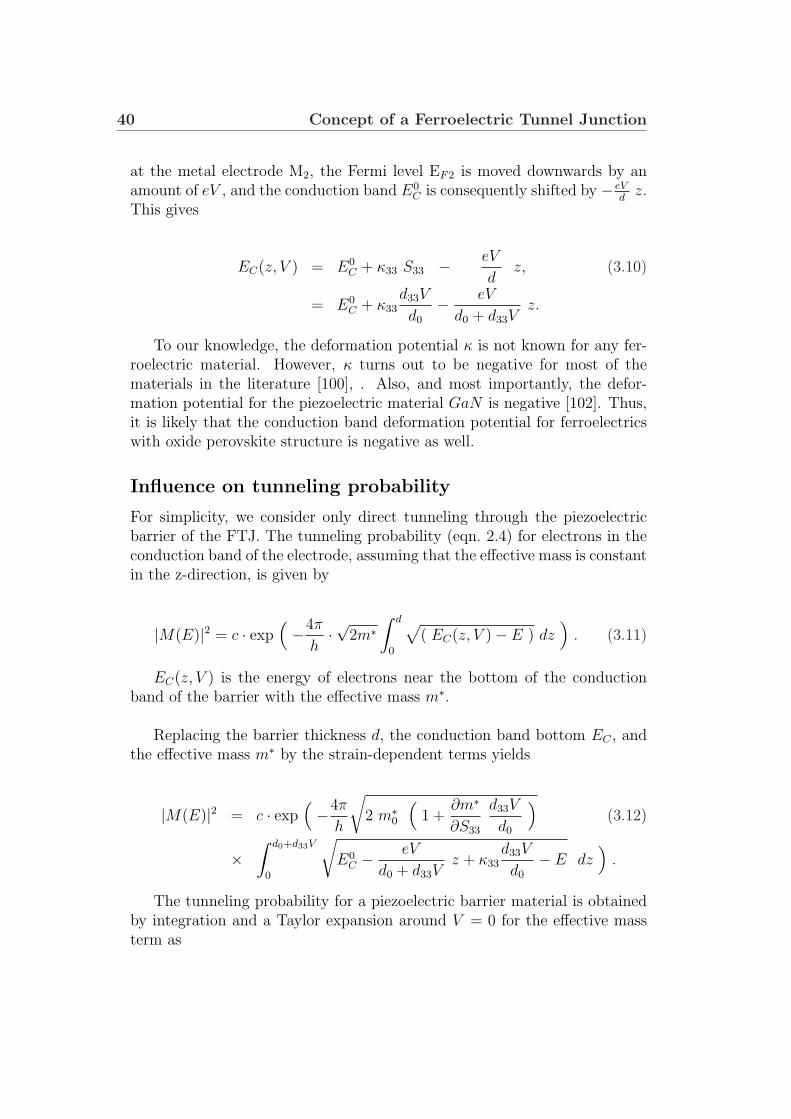
40 Concept of a Ferroelectric Tunnel Junction
at the metal electrode M2, the Fermi level EF2 is moved downwards by anamount of eV , and the conduction band E0
C is consequently shifted by − eVd
z.This gives
EC(z, V ) = E0C + κ33 S33 − eV
dz, (3.10)
= E0C + κ33
d33V
d0
− eV
d0 + d33Vz.
To our knowledge, the deformation potential κ is not known for any fer-roelectric material. However, κ turns out to be negative for most of thematerials in the literature [100], . Also, and most importantly, the defor-mation potential for the piezoelectric material GaN is negative [102]. Thus,it is likely that the conduction band deformation potential for ferroelectricswith oxide perovskite structure is negative as well.
Influence on tunneling probability
For simplicity, we consider only direct tunneling through the piezoelectricbarrier of the FTJ. The tunneling probability (eqn. 2.4) for electrons in theconduction band of the electrode, assuming that the effective mass is constantin the z-direction, is given by
|M(E)|2 = c · exp(−4π
h·√
2m∗∫ d
0
√( EC(z, V )− E ) dz
). (3.11)
EC(z, V ) is the energy of electrons near the bottom of the conductionband of the barrier with the effective mass m∗.
Replacing the barrier thickness d, the conduction band bottom EC , andthe effective mass m∗ by the strain-dependent terms yields
|M(E)|2 = c · exp(−4π
h
√2 m∗
0
(1 +
∂m∗
∂S33
d33V
d0
)(3.12)
×∫ d0+d33V
0
√E0
C −eV
d0 + d33Vz + κ33
d33V
d0
− E dz)
.
The tunneling probability for a piezoelectric barrier material is obtainedby integration and a Taylor expansion around V = 0 for the effective massterm as
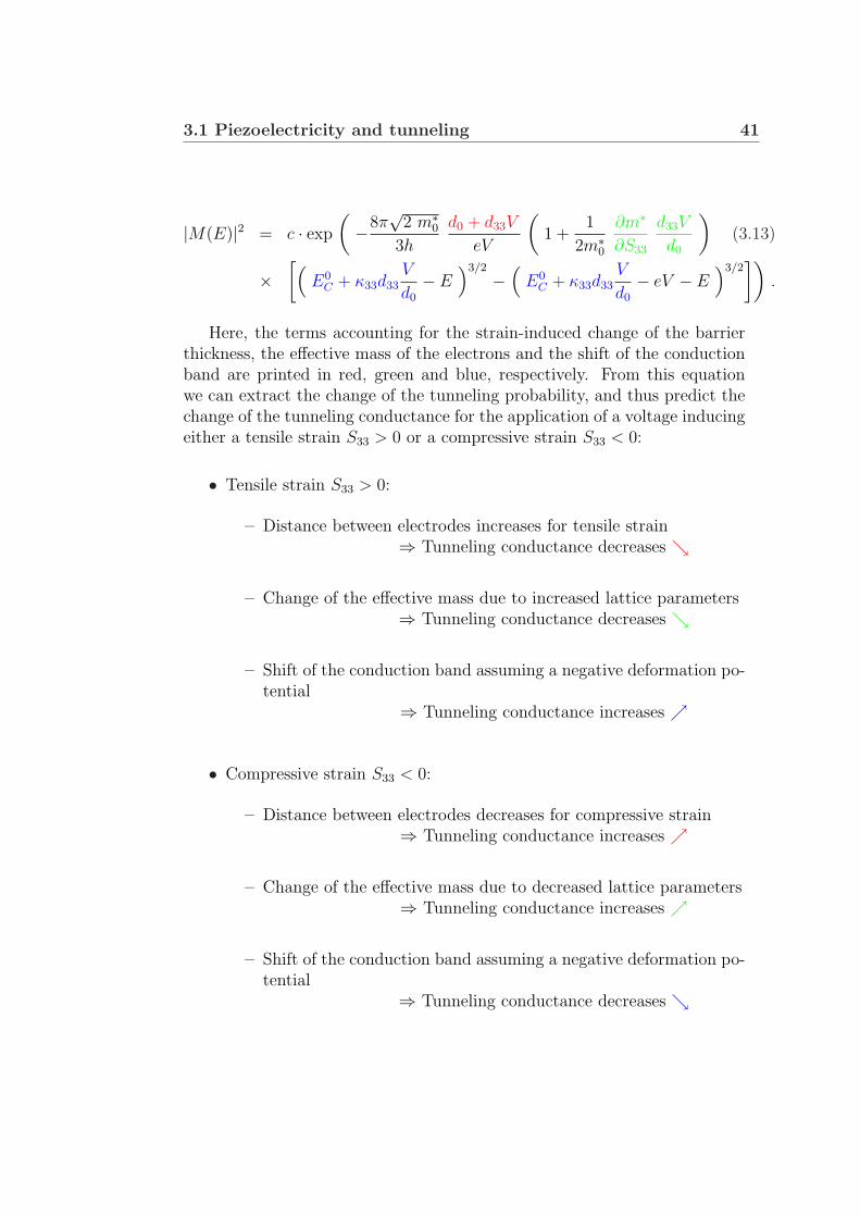
3.1 Piezoelectricity and tunneling 41
|M(E)|2 = c · exp
(−8π
√2 m∗
0
3h
d0 + d33V
eV
(1 +
1
2m∗0
∂m∗
∂S33
d33V
d0
)(3.13)
×[(
E0C + κ33d33
V
d0
− E)3/2
−(
E0C + κ33d33
V
d0
− eV − E)3/2
]).
Here, the terms accounting for the strain-induced change of the barrierthickness, the effective mass of the electrons and the shift of the conductionband are printed in red, green and blue, respectively. From this equationwe can extract the change of the tunneling probability, and thus predict thechange of the tunneling conductance for the application of a voltage inducingeither a tensile strain S33 > 0 or a compressive strain S33 < 0:
• Tensile strain S33 > 0:
– Distance between electrodes increases for tensile strain⇒ Tunneling conductance decreases
– Change of the effective mass due to increased lattice parameters⇒ Tunneling conductance decreases
– Shift of the conduction band assuming a negative deformation po-tential
⇒ Tunneling conductance increases
• Compressive strain S33 < 0:
– Distance between electrodes decreases for compressive strain⇒ Tunneling conductance increases
– Change of the effective mass due to decreased lattice parameters⇒ Tunneling conductance increases
– Shift of the conduction band assuming a negative deformation po-tential
⇒ Tunneling conductance decreases
42 Concept of a Ferroelectric Tunnel Junction
Here, the colors of the arrows correspond to the color code used above.Assuming that the deformation potential is negative (see p. 40), there is nounambiguous behavior of the tunneling conductance for tensile or compres-sive strain. Indeed, we cannot predict an increasing or a decreasing tunnel-ing conductance for a given voltage-induced strain. Nevertheless, unless thethree effects discussed above compensate each other, a strain-induced changeof the tunneling conductance, and thus, a strain-induced change of the tunnelcurrent is expected for a piezoelectric barrier.
3.2 Ferroelectricity and tunneling
Fig. 3.3 (upper part) shows the strain produced in a ferroelectric materialby the application of a voltage. This converse piezoelectric effect for a fer-roelectric material differs from that for a piezoelectric, but not ferroelectricmaterial, only by the existence of two linear curves (one for each polarizationstate) and the jump from negative to positive strain at the coercive volt-ages ±Vc. The free energy as a function of the polarization is plotted in thelower part of Fig. 3.3. The blue balls in plots (a)-(e) indicate the specificfree energies FP = F (P ) at the corresponding strain-field positions. The freeenergy functional possesses three extrema. Two of them are stable (i.e. theminima indicated by the blue ball in (b) and (e)). They correspond to thestable polarization states of the ferroelectric thin film at V = 0 volts andP = ±Pr 6= 0. The third extremum of the free energy FP is unstable. Thisextremum corresponds to the voltages V = ±Vc and coincides with a jumpin the strain from a negative to a positive value (e.g. (c)).
No clear behavior has been obtained in our theoretical treatments of thetunneling conductance for a given voltage-induced strain in a piezoelectricmaterial. Both the strain effects on the barrier thickness and the effectivemass of electrons inside the barrier result in qualitatively similar changes ofthe tunneling conductance, whereas the effect on the position of the conduc-tion band results in the opposite impact on the tunneling conductance. Atpresent, no numerical calculations including all three effects discussed aboveare possible, due to a lack of knowledge of the deformation potential andthe exact strain dependence of the effective mass of electrons. It is, how-ever, possible to simulate the effect of a strain-induced change of the barrierthickness on the tunnel current through a ferroelectric tunnel junction. Thiswill enable us to get a feeling as to what extent the expected influence ofthe converse piezoelectric effect on the barrier thickness may alter the I-Vcharacteristic of an FTJ.
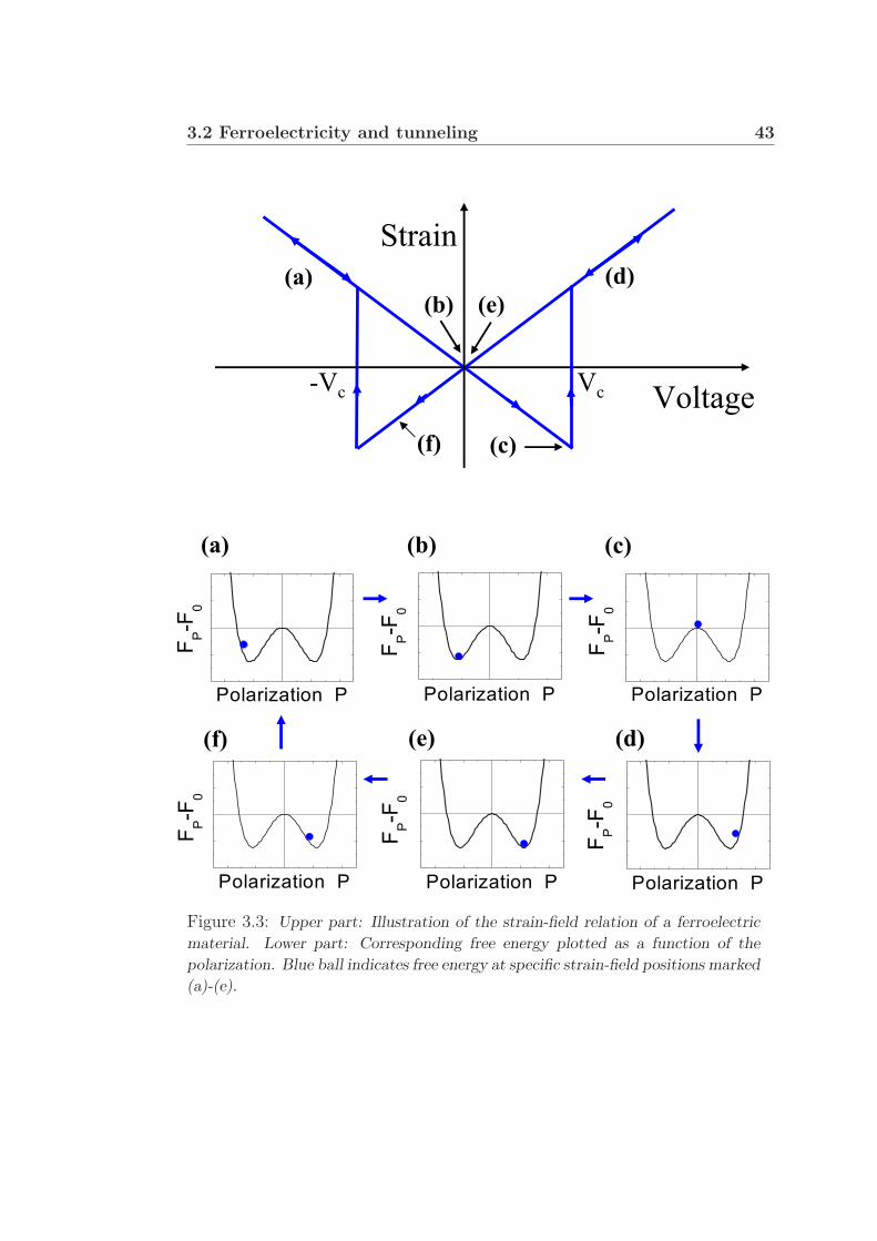
3.2 Ferroelectricity and tunneling 43
Strain
VoltageVc-Vc
(d)
(b) (e)
(f) (c)
(a)
Polarization P
FP-F
0
Polarization P
FP-F
0
(a) (b)
Polarization P
FP-F
0
(c)
Polarization P
FP-F
0
(d)
Polarization P
FP-F
0
(e)
Polarization P
FP-F
0
(f)
Figure 3.3: Upper part: Illustration of the strain-field relation of a ferroelectric
material. Lower part: Corresponding free energy plotted as a function of the
polarization. Blue ball indicates free energy at specific strain-field positions marked
(a)-(e).
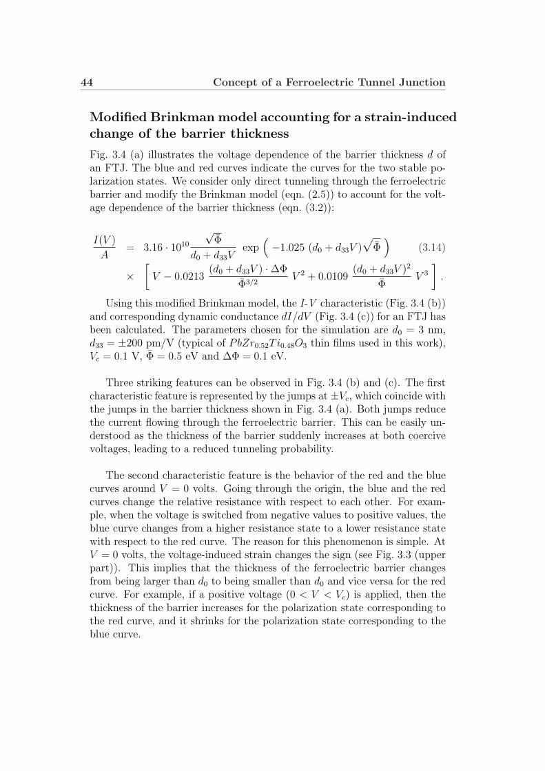
44 Concept of a Ferroelectric Tunnel Junction
Modified Brinkman model accounting for a strain-inducedchange of the barrier thickness
Fig. 3.4 (a) illustrates the voltage dependence of the barrier thickness d ofan FTJ. The blue and red curves indicate the curves for the two stable po-larization states. We consider only direct tunneling through the ferroelectricbarrier and modify the Brinkman model (eqn. (2.5)) to account for the volt-age dependence of the barrier thickness (eqn. (3.2)):
I(V )
A= 3.16 · 1010
√Φ
d0 + d33Vexp
(−1.025 (d0 + d33V )
√Φ
)(3.14)
×[
V − 0.0213(d0 + d33V ) ·∆Φ
Φ3/2V 2 + 0.0109
(d0 + d33V )2
ΦV 3
].
Using this modified Brinkman model, the I-V characteristic (Fig. 3.4 (b))and corresponding dynamic conductance dI/dV (Fig. 3.4 (c)) for an FTJ hasbeen calculated. The parameters chosen for the simulation are d0 = 3 nm,d33 = ±200 pm/V (typical of PbZr0.52Ti0.48O3 thin films used in this work),Vc = 0.1 V, Φ = 0.5 eV and ∆Φ = 0.1 eV.
Three striking features can be observed in Fig. 3.4 (b) and (c). The firstcharacteristic feature is represented by the jumps at ±Vc, which coincide withthe jumps in the barrier thickness shown in Fig. 3.4 (a). Both jumps reducethe current flowing through the ferroelectric barrier. This can be easily un-derstood as the thickness of the barrier suddenly increases at both coercivevoltages, leading to a reduced tunneling probability.
The second characteristic feature is the behavior of the red and the bluecurves around V = 0 volts. Going through the origin, the blue and the redcurves change the relative resistance with respect to each other. For exam-ple, when the voltage is switched from negative values to positive values, theblue curve changes from a higher resistance state to a lower resistance statewith respect to the red curve. The reason for this phenomenon is simple. AtV = 0 volts, the voltage-induced strain changes the sign (see Fig. 3.3 (upperpart)). This implies that the thickness of the ferroelectric barrier changesfrom being larger than d0 to being smaller than d0 and vice versa for the redcurve. For example, if a positive voltage (0 < V < Vc) is applied, then thethickness of the barrier increases for the polarization state corresponding tothe red curve, and it shrinks for the polarization state corresponding to theblue curve.
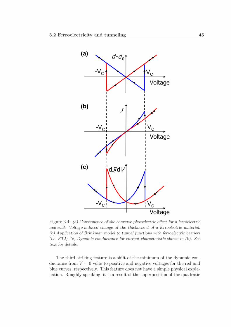
3.2 Ferroelectricity and tunneling 45
d -d 0
Voltage
Voltage
J
Voltage
dJ/dV
(a)
(b)
(c)
VC
-VC
-VC
-VC
VC
VC
Figure 3.4: (a) Consequence of the converse piezoelectric effect for a ferroelectric
material: Voltage-induced change of the thickness d of a ferroelectric material.
(b) Application of Brinkman model to tunnel junctions with ferroelectric barriers
(i.e. FTJ). (c) Dynamic conductance for current characteristic shown in (b). See
text for details.
The third striking feature is a shift of the minimum of the dynamic con-ductance from V = 0 volts to positive and negative voltages for the red andblue curves, respectively. This feature does not have a simple physical expla-nation. Roughly speaking, it is a result of the superposition of the quadratic
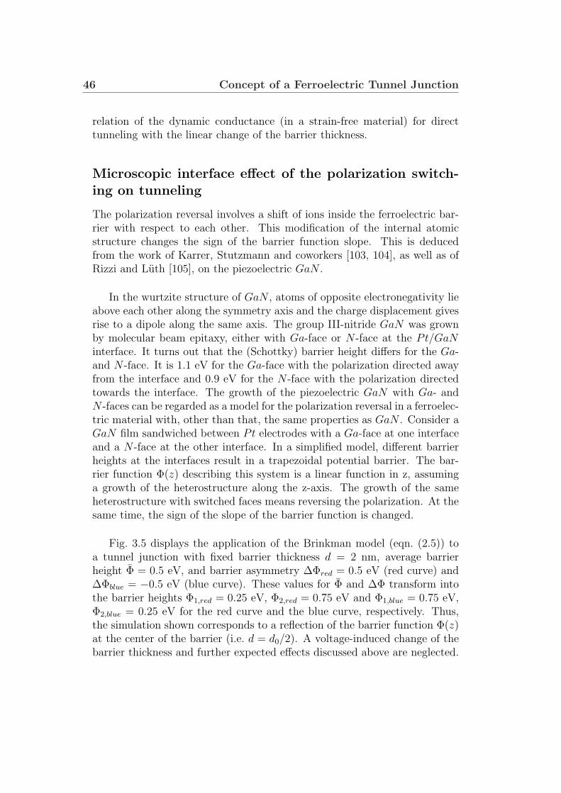
46 Concept of a Ferroelectric Tunnel Junction
relation of the dynamic conductance (in a strain-free material) for directtunneling with the linear change of the barrier thickness.
Microscopic interface effect of the polarization switch-ing on tunneling
The polarization reversal involves a shift of ions inside the ferroelectric bar-rier with respect to each other. This modification of the internal atomicstructure changes the sign of the barrier function slope. This is deducedfrom the work of Karrer, Stutzmann and coworkers [103, 104], as well as ofRizzi and Luth [105], on the piezoelectric GaN .
In the wurtzite structure of GaN , atoms of opposite electronegativity lieabove each other along the symmetry axis and the charge displacement givesrise to a dipole along the same axis. The group III-nitride GaN was grownby molecular beam epitaxy, either with Ga-face or N -face at the Pt/GaNinterface. It turns out that the (Schottky) barrier height differs for the Ga-and N -face. It is 1.1 eV for the Ga-face with the polarization directed awayfrom the interface and 0.9 eV for the N -face with the polarization directedtowards the interface. The growth of the piezoelectric GaN with Ga- andN -faces can be regarded as a model for the polarization reversal in a ferroelec-tric material with, other than that, the same properties as GaN . Consider aGaN film sandwiched between Pt electrodes with a Ga-face at one interfaceand a N -face at the other interface. In a simplified model, different barrierheights at the interfaces result in a trapezoidal potential barrier. The bar-rier function Φ(z) describing this system is a linear function in z, assuminga growth of the heterostructure along the z-axis. The growth of the sameheterostructure with switched faces means reversing the polarization. At thesame time, the sign of the slope of the barrier function is changed.
Fig. 3.5 displays the application of the Brinkman model (eqn. (2.5)) toa tunnel junction with fixed barrier thickness d = 2 nm, average barrierheight Φ = 0.5 eV, and barrier asymmetry ∆Φred = 0.5 eV (red curve) and∆Φblue = −0.5 eV (blue curve). These values for Φ and ∆Φ transform intothe barrier heights Φ1,red = 0.25 eV, Φ2,red = 0.75 eV and Φ1,blue = 0.75 eV,Φ2,blue = 0.25 eV for the red curve and the blue curve, respectively. Thus,the simulation shown corresponds to a reflection of the barrier function Φ(z)at the center of the barrier (i.e. d = d0/2). A voltage-induced change of thebarrier thickness and further expected effects discussed above are neglected.
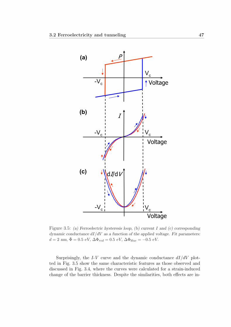
3.2 Ferroelectricity and tunneling 47
Voltage
I
Voltage
dI/dV
(b)
(c)
-Vc
-Vc
Vc
Vc
Voltage-Vc
Vc
P(a)
Figure 3.5: (a) Ferroelectric hysteresis loop, (b) current I and (c) corresponding
dynamic conductance dI/dV as a function of the applied voltage. Fit parameters:
d = 2 nm, Φ = 0.5 eV, ∆Φred = 0.5 eV, ∆Φblue = −0.5 eV.
Surprisingly, the I-V curve and the dynamic conductance dI/dV plot-ted in Fig. 3.5 show the same characteristic features as those observed anddiscussed in Fig. 3.4, where the curves were calculated for a strain-inducedchange of the barrier thickness. Despite the similarities, both effects are in-
48 Concept of a Ferroelectric Tunnel Junction
dependent of each other. By changing the sign of ∆Φ, only the quadraticterm in the voltage in the Brinkman equation (eqn. 2.5) is changed. For apositive ∆Φ, the current-voltage curve is shifted downwards by a quadraticterm in voltage and vice versa for a negative ∆Φ. As a result, the currentfor the red curve I∆Φ>0 with respect to the current for the blue curve I∆Φ<0
is reduced for positive voltages and it is enhanced for negative voltages. Theshift in voltage observed for the dynamic conductance is a simple mathe-matical consequence. The quadratic term in voltage that is changed in theBrinkman equation becomes linear for its derivative. Hence, a change of thesign of ∆Φ results in a shift of the dynamic conductance along the voltageaxis.
As a conclusion to this Chapter, we have presented the concept of aferroelectric tunnel junction and called this novel device an FTJ. Theoret-ical calculations were presented to determine the influence of the conversepiezoelectric effect on the direct tunnel current of a tunnel junction with apiezoelectric or ferroelectric barrier. Three effects have been identified lead-ing to a strain-induced change of the tunnel current. It is expected that thethickness of the barrier changes, the effective mass changes, and that thepositions of the conduction and valence band edges shift when a voltage isapplied to an FTJ producing a strain in the barrier material. Unfortunately,only two of these effects, namely the change of the barrier thickness and thechange of the effective mass, have the same consequence (i.e. the tunnelingconductance decreases for tensile strain), whereas an increase of the tunnel-ing conductance is expected for tensile strain, arising from a change of theposition of the conduction band edge. Thus, we cannot unambiguously pre-dict the consequence of the converse piezoelectric effect on the tunnel current.Nevertheless, we have calculated the I-V characteristic and the dynamic con-ductance for a tunnel junction accounting for two different effects. First, avoltage-induced change of the barrier thickness was modelled by modifyingthe Brinkman theory. Second, the microscopic interface effect was consid-ered, resulting from the switching of the polarization and leading to a changeof the atomic structure. Using typical parameters for PbZr0.52Ti0.48O3, a fer-roelectric material studied in this work, in both cases clearly different curveswere obtained for two oppositely directed polarization states. Particularly,these simulations show that the mentioned effects on the tunnel current arelarge and should be observable in experimental direct tunneling curves aswell.
Chapter 4
Heteroepitaxy of oxideperovskites
Perovskite is named for a Russian mineralogist, Count Lev Aleksevich vonPerovski. The mineral was discovered and named by Gustav Rose in 1839from samples found in the Ural Mountains.
Functional oxide perovskites are receiving more and more attention dueto their unique dielectric, pyroelectric, piezoelectric, ferroelectric, magneticand superconducting properties.
This Chapter deals with the perovskite materials used within this workand with the deposition methods employed for their growth.
4.1 Material systems
The heterostructures that have been primarily studied in this PhD thesisare Pt (or SrRuO3) / PbZr0.52Ti0.48O3 / SrRuO3 and Pt (or SrRuO3) /(Ba, Sr)TiO3 / SrRuO3, both grown on SrT iO3 (100) substrates. In thisChapter a brief description of the materials used, excluding Pt1, will begiven. The main emphasis will be on the properties which led to the specificmaterial being chosen for use in this work. In addition, some properties willbe mentioned which, in the author’s opinion, are interesting. The followingSections, however, should not be regarded as comprehensive lists of the prop-erties of these materials.
1Pt served as the top electrode and was either sputtered or e-beam-evaporated byTh. Schneller, RWTH Aachen, or H. Haselier, Forschungszentrum Julich, respectively.
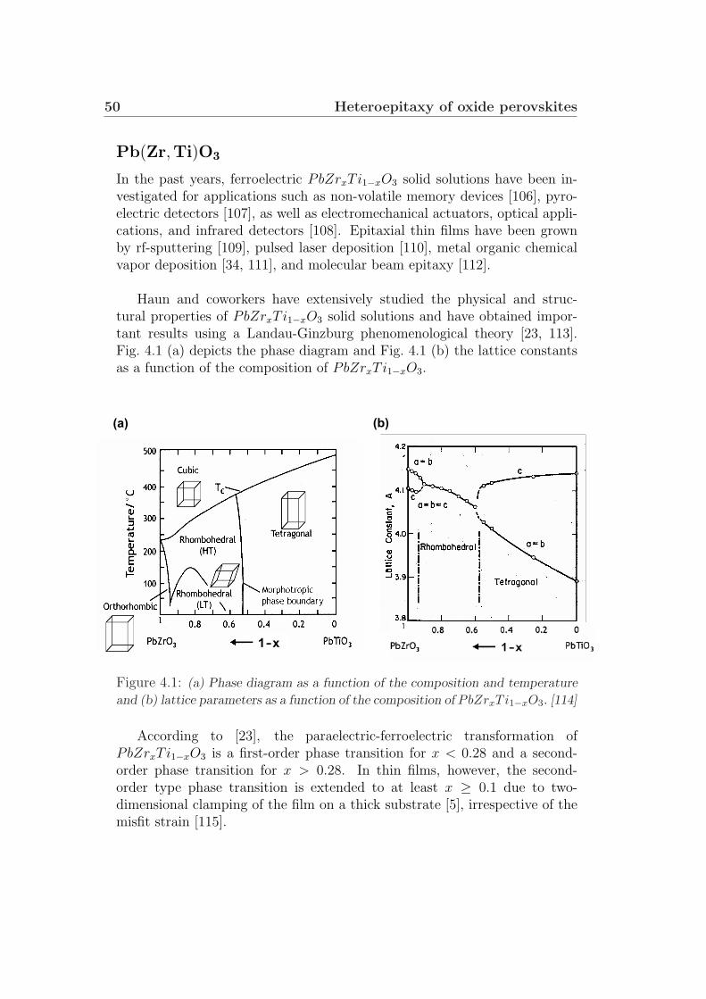
50 Heteroepitaxy of oxide perovskites
Pb(Zr,Ti)O3
In the past years, ferroelectric PbZrxTi1−xO3 solid solutions have been in-vestigated for applications such as non-volatile memory devices [106], pyro-electric detectors [107], as well as electromechanical actuators, optical appli-cations, and infrared detectors [108]. Epitaxial thin films have been grownby rf-sputtering [109], pulsed laser deposition [110], metal organic chemicalvapor deposition [34, 111], and molecular beam epitaxy [112].
Haun and coworkers have extensively studied the physical and struc-tural properties of PbZrxTi1−xO3 solid solutions and have obtained impor-tant results using a Landau-Ginzburg phenomenological theory [23, 113].Fig. 4.1 (a) depicts the phase diagram and Fig. 4.1 (b) the lattice constantsas a function of the composition of PbZrxTi1−xO3.
1-x
(a) (b)
Figure 4.1: (a) Phase diagram as a function of the composition and temperature
and (b) lattice parameters as a function of the composition of PbZrxTi1−xO3. [114]
According to [23], the paraelectric-ferroelectric transformation ofPbZrxTi1−xO3 is a first-order phase transition for x < 0.28 and a second-order phase transition for x > 0.28. In thin films, however, the second-order type phase transition is extended to at least x ≥ 0.1 due to two-dimensional clamping of the film on a thick substrate [5], irrespective of themisfit strain [115].
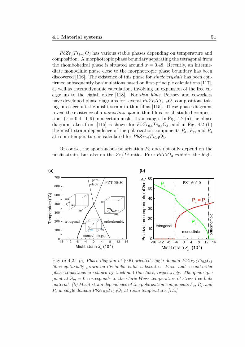
4.1 Material systems 51
PbZrxTi1−xO3 has various stable phases depending on temperature andcomposition. A morphotropic phase boundary separating the tetragonal fromthe rhombohedral phase is situated around x = 0.48. Recently, an interme-diate monoclinic phase close to the morphotropic phase boundary has beendiscovered [116]. The existence of this phase for single crystals has been con-firmed subsequently by simulations based on first-principle calculations [117],as well as thermodynamic calculations involving an expansion of the free en-ergy up to the eighth order [118]. For thin films, Pertsev and coworkershave developed phase diagrams for several PbZrxTi1−xO3 compositions tak-ing into account the misfit strain in thin films [115]. These phase diagramsreveal the existence of a monoclinic gap in thin films for all studied composi-tions (x = 0.4−0.9) in a certain misfit strain range. In Fig. 4.2 (a) the phasediagram taken from [115] is shown for PbZr0.5Ti0.5O3, and in Fig. 4.2 (b)the misfit strain dependence of the polarization components Px, Py, and Pz
at room temperature is calculated for PbZr0.6Ti0.4O3.
Of course, the spontaneous polarization PS does not only depend on themisfit strain, but also on the Zr/T i ratio. Pure PbT iO3 exhibits the high-
0
100
200
300
400
500
600
700
-16 -12 -8 -4 0 4 8 12 16
monoclinic gap
orthorhombicTem
pera
ture
(°C
)
para-
electric
tetragonal
PZT 50/50
Misfit strain Sm (10
-3)
(a) (b)
-16 -12 -8 -4 0 4 8 12 160
10
20
30
40
50
60
Pz
Px = P
y
Pz
ort
ho
rho
mb
ic
monoclinic
tetragonal
PZT 60/40
Misfit strain Sm (10
-3)
Pola
rization c
om
ponents
(µC
/cm
2)
Figure 4.2: (a) Phase diagram of (00l)-oriented single domain PbZr0.5Ti0.5O3
films epitaxially grown on dissimilar cubic substrates. First- and second-order
phase transitions are shown by thick and thin lines, respectively. The quadruple
point at Sm = 0 corresponds to the Curie-Weiss temperature of stress-free bulk
material. (b) Misfit strain dependence of the polarization components Px, Py, and
Pz in single domain PbZr0.6Ti0.4O3 at room temperature. [115]

52 Heteroepitaxy of oxide perovskites
est spontaneous polarization of 81 µC/cm2. PS decreases with increasingZr-content. For PbZr0.52Ti0.48O3, a value of 49 µC/cm2 has been deter-mined [23]. PbZrxTi1−xO3 close to the morphotropic phase boundary ex-hibits the strongest piezoelectric effect [14]. In fact, PbZr0.52Ti0.48O3 waschosen for this work as a ferroelectric film because this composition com-bines a large spontaneous polarization with the strongest piezoelectric effect.
Pb(Zr, T i)O3 has a composition-dependent band gap of about 3 eV, incontrast to Eg ≈ 9 eV for conventional dielectrics, such as SiO2 [22]. There-fore, a significant electronic conduction can be present in this material. BulkPb(Zr, T i)O3 is often considered to be p-type conductive due to holes gen-erated by the presence of lattice vacancies [119, 120], but there are alsoreferences in the literature according to which it is mixed or n-type conduc-tive [26]. In comparison to other semiconductors, such as Si (Eg = 1.12 eV,m∗ ≈ 10−1 m0) and GaAs (Eg = 1.42 eV, m∗ = 6.6 · 10−2 m0) [121, 97],the band gap of Pb(Zr, T i)O3 is very high and the electronic effective massis low (m∗ ≈ 10−3 m0) [122]. Assuming a perfectly ionic and trap-free fer-roelectric material, one can calculate the barrier height from the differencebetween the metal work function and the electron affinity of the ferroelectric.Experimental values, however, are usually smaller, thus the barrier height isoften calculated from a different relationship given in [123]. Experimentalvalues for the barrier height of Pt/Pb(Zr, T i)O3 and SrRuO3/Pb(Zr, T i)O3
are 0.6 eV [122] and approximately 0.35 eV [123], respectively.
(Ba,Sr)TiO3
High-permittivity (high-k) materials have been investigated for many years.One of the most promising materials for future, high-density dynamic randomaccess memories (DRAM) is (Ba, Sr)TiO3 because of its high dielectric con-stant [124]. Epitaxial thin films have been grown by rf-sputtering [125, 126],pulsed laser deposition [127], metal organic chemical vapor deposition [128],and molecular beam epitaxy [129, 130, 131, 132, 133].
As illustrated in Fig. 4.3, the ferroelectric transition of (Ba, Sr)TiO3 sin-gle crystals can be shifted in temperature by adjusting the Ba to Sr ratio.BaTiO3 is a ferroelectric material with a Curie temperature of 120 C, whileSrT iO3 is a paraelectric with no confirmed ferroelectric phase transition (seep. 55). At room temperature, the solid solution system is in a ferroelectricphase when the Ba content is in the range from 0.7 to 1.0, and in a para-electric phase for a lower Ba content. Bulk BaTiO3 undergoes a first-orderparaelectric to ferroelectric phase transition. However, as it was the case
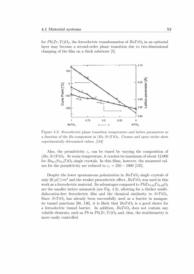
4.1 Material systems 53
for Pb(Zr, T i)O3, the ferroelectric transformation of BaTiO3 in an epitaxiallayer may become a second-order phase transition due to two-dimensionalclamping of the film on a thick substrate [5].
4.15
4.05
3.95
3.90
3.85
Latt
ice
para
mete
r[Å
]
1 0.75 0.5 0.25 0
BaTiO3 SrTiO3x
Cu
rie
Po
int
[°C
]
-200
-100
0
100
Figure 4.3: Ferroelectric phase transition temperature and lattice parameters as
a function of the Ba-component in (Ba, Sr)TiO3. Crosses and open circles show
experimentally determined values. [134]
Also, the permittivity εr can be tuned by varying the composition of(Ba, Sr)TiO3. At room temperature, it reaches its maximum of about 12,000for Ba0.7Sr0.3TiO3 single crystals. In thin films, however, the measured val-ues for the permittivity are reduced to εr = 250− 1000 [135].
Despite the lower spontaneous polarization in BaTiO3 single crystals ofonly 26 µC/cm2 and the weaker piezoelectric effect, BaTiO3 was used in thiswork as a ferroelectric material. Its advantages compared to PbZr0.52Ti0.48O3
are the smaller lattice mismatch (see Fig. 4.3), allowing for a thicker misfit-dislocation-free ferroelectric film and the chemical similarity to SrT iO3.Since SrT iO3 has already been successfully used as a barrier in mangan-ite tunnel junctions [80, 136], it is likely that BaTiO3 is a good choice fora ferroelectric tunnel barrier. In addition, BaTiO3 does not contain anyvolatile elements, such as Pb in Pb(Zr, T i)O3 and, thus, the stoichiometry ismore easily controlled.

54 Heteroepitaxy of oxide perovskites
According to Hartmann and coworkers [123], the barrier height ofSrRuO3/(Ba, Sr)TiO3 is similar to that of SrRuO3/Pb(Zr, T i)O3 of ap-proximately 0.35 eV.
SrRuO3
SrRuO3 has been studied extensively and has become a widely used epitaxialelectrode for perovskite ferroelectric materials. Single crystalline SrRuO3 isa pseudo-cubic perovskite and a metallic conductor with a paramagnetic toferromagnetic phase transition at 160 K [137]. Its work function is smallerthan that of Pt of 5.3 eV [26]. It is 5.0 eV if SrRuO3 is fully oxidized, and itis reduced to 4.6 eV in the case of oxygen deficiency [123]. Most reports onbulk materials indicate that its crystal structure is orthorhombic with latticeparameters of a = 5.55 A, b = 5.56 A, and c = 7.84 A [138, 139]. Threedifferent phases have been found between 10 K and 1273 K [140, 141, 142].Epitaxial thin films have been grown by sputtering [143], pulsed laser de-position [144, 145, 146], metal organic chemical vapor deposition [147], andmolecular beam epitaxy [148, 149] on SrT iO3 and LaAlO3 substrates.
SrRuO3 is an excellent electrode for the growth of a variety of ferroelectricmaterials, including Pb(Zr, T i)O3 and BaTiO3. In addition to its perovskitecrystal structure and pseudo-cubic lattice constant of 3.93 A [150], whichprovide excellent structural compatibility with these ferroelectrics, SrRuO3
has been shown to significantly reduce fatigue in these materials [151] - animportant advantage over metal electrodes [152].
SrTiO3 (100) substrate
The choice of the substrate material is of great importance for the epitaxialgrowth of heterostructures. On the one hand, the growth of high-qualityepitaxial materials requires substrates with structural and chemical compat-ibility to avoid structural defects, including dislocations, cracking, or even acomplete loss of epitaxy, as well as interfacial reaction layers or interdiffusionof unwanted elements into the film. On the other hand, I have extensivelydiscussed the influence of mechanical boundary conditions on the ferroelec-tric properties of thin films (Chap. 1.4). Strain induced by the much thickersubstrate may alter the single crystal lattice parameters, shift the tempera-ture of the paraelectric to ferroelectric phase transition, and even change theorder of this phase transition in epitaxial thin films.

4.2 Deposition techniques 55
In view of the above mentioned considerations, (100)-oriented SrT iO3
was chosen as substrate material. It represents an insulating and compres-sive substrate for the SrRuO3 bottom electrode and the Pb(Zr, T i)O3 and(Ba, Sr)TiO3 ferroelectric thin films. It thus allows for an epitaxial high-crystalline growth of these thin films and stabilizes the ferroelectric phase inthe out-of-plane direction.
SrT iO3 is a quantum paraelectric material that exhibits an increase inthe dielectric constant as it is cooled [153]. It shows a structural phase tran-sition to a tetragonal phase at 105 K [154]. Ferroelectricity in slightly off-stoichiometric SrT ixO3−δ has been demonstrated [155, 156, 157]. However,in pure SrT iO3 crystals, the ferroelectric transition is not observed. There-fore, this compound is regarded as an incipient ferroelectric. It is expected,however, that the situation may change dramatically in SrT iO3 epitaxialthin films. SrT iO3 thin films grown on a sufficiently compressive or tensilesubstrate have been predicted to exhibit ferroelectricity at room temperaturein the out-of-plane or in-plane direction, respectively [154].
4.2 Deposition techniques
Although significant time was spent to set up a high-pressure sputtering sys-tem and learning the complex growth techniques of molecular beam epitaxy,the description of these techniques will be brief. Additional information canbe found in Refs. [158, 159].
A large variety of thin film deposition methods have been developed inthe last decades. The choice of the best method is difficult and depends onthe specific material to be grown on a specific substrate and the purpose ofthe deposited film. The deposition techniques can be divided into physicalvapor deposition and chemical vapor deposition. Physical methods are char-acterized by a particle source and generally a free flight to the substrate. Forchemical methods, so-called precursor molecules fill the reactor vessel as avapor, dissociate at the hot substrate surface and release the atoms to bedeposited [159].
One of the main differences between the different physical vapor depo-sition techniques is the mean free path of the atoms or molecules. This isthe distance that a particle travels, on the average, before experiencing acollision. Assuming that gas atoms may be considered as non interactingwith a Maxwell velocity distribution the mean free path λ of the atoms ormolecules is obtained:
56 Heteroepitaxy of oxide perovskites
λ =1√
2πNd2(4.1)
where d is the molecular diameter and N the concentration of the gas [159].Substituting N by the law of the ideal gas N = p/kBT yields
λ =kBT√2πpd2
. (4.2)
For instance, the mean free path at a typical growth temperature of 600Cin oxygen (d = 370 pm) is given by
λ =1.98 10−2
p [mbar]cm. (4.3)
In the following Sections, the physical vapor deposition techniques used inthis work will be described. High-pressure sputtered SrRuO3 andPbZr0.52Ti0.48O3 thin films, as well as SrRuO3 and BaTiO3 thin films bymolecular beam epitaxy, were grown by the author himself, whereas pulsedlaser deposited BaTiO3 thin films were provided by J. Schubert and his groupat ISG, Forschungszentrum Julich.
Pulsed laser deposition
Pulsed laser deposition (PLD) is a physical vapor deposition technique allow-ing the growth of high-quality films with high growth rates (a typical growthrate is 1 nm/s). A sketch of the PLD-system is shown in Fig. 4.4 (a). Apulsed laser beam from an excimer laser2 is focused onto a rotating targetin a gas pressure environment of about 10−3 mbar. A plasma (Fig. 4.4 (b))containing energetic neutral atoms, ions and molecules is formed as a resultof the high energy density of 2−5 J/cm2 at the target surface and reaches thesubstrate surface with a broad energy distribution of 0.1 eV to > 10 eV [159].
PLD has been used successfully to grow numerous perovskites exhibitingsuperconducting [160, 161] or ferroelectric properties [162]. For example,1 µm thick BaTiO3 films have been prepared by PLD for electro-opticalapplications [127]. These films grown on MgO substrates have been used forwaveguides with low optical losses.
2for instance, KrF excimer laser with a wavelength of 248 nm and a repetition rate of10 Hz
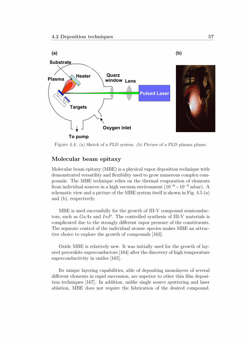
4.2 Deposition techniques 57
(b)
Linse
Targets
Substrat +Heizer
Plasma
Pumpen
Gaseinlaß
Quarz-fenster
To pump
Oxygen inlet
Lenswindow
Substrate
Quarz
Pulsed Laser
Heater
(a)
Targets
Plasma
Figure 4.4: (a) Sketch of a PLD system. (b) Picture of a PLD plasma plume.
Molecular beam epitaxy
Molecular beam epitaxy (MBE) is a physical vapor deposition technique withdemonstrated versatility and flexibility used to grow numerous complex com-pounds. The MBE technique relies on the thermal evaporation of elementsfrom individual sources in a high vacuum environment (10−6−10−9 mbar). Aschematic view and a picture of the MBE system itself is shown in Fig. 4.5 (a)and (b), respectively.
MBE is used successfully for the growth of III-V compound semiconduc-tors, such as GaAs and InP . The controlled synthesis of III-V materials iscomplicated due to the strongly different vapor pressure of the constituents.The separate control of the individual atomic species makes MBE an attrac-tive choice to explore the growth of compounds [163].
Oxide MBE is relatively new. It was initially used for the growth of lay-ered perovskite superconductors [164] after the discovery of high temperaturesuperconductivity in oxides [165].
Its unique layering capabilities, able of depositing monolayers of severaldifferent elements in rapid succession, are superior to other thin film deposi-tion techniques [167]. In addition, unlike single source sputtering and laserablation, MBE does not require the fabrication of the desired compound.
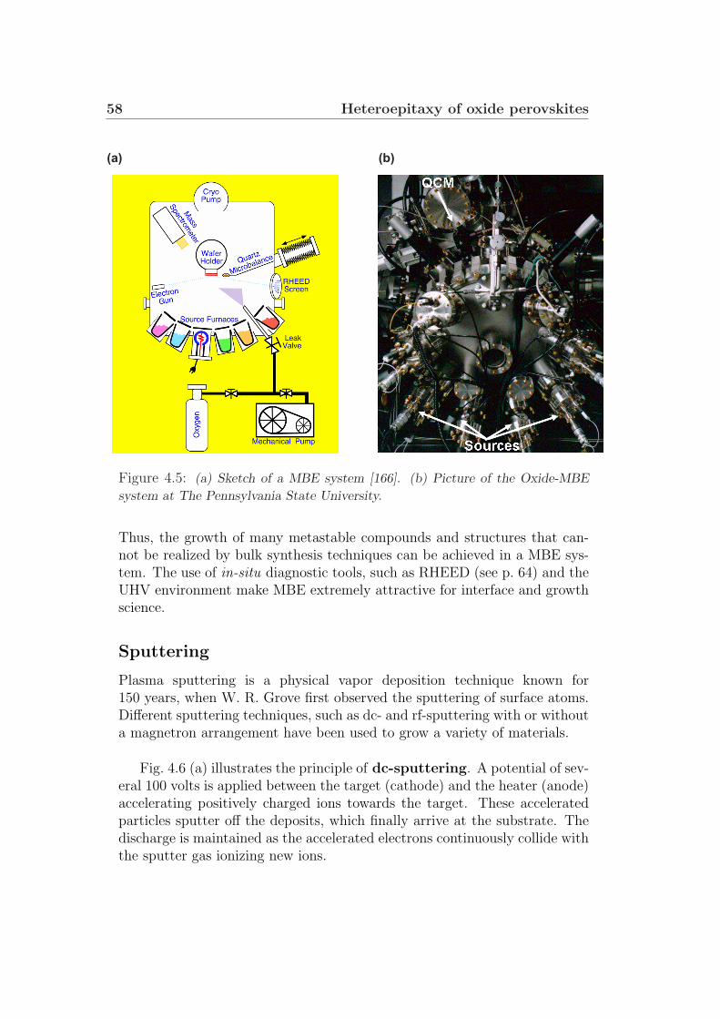
58 Heteroepitaxy of oxide perovskites
(a) (b)
Figure 4.5: (a) Sketch of a MBE system [166]. (b) Picture of the Oxide-MBE
system at The Pennsylvania State University.
Thus, the growth of many metastable compounds and structures that can-not be realized by bulk synthesis techniques can be achieved in a MBE sys-tem. The use of in-situ diagnostic tools, such as RHEED (see p. 64) and theUHV environment make MBE extremely attractive for interface and growthscience.
Sputtering
Plasma sputtering is a physical vapor deposition technique known for150 years, when W. R. Grove first observed the sputtering of surface atoms.Different sputtering techniques, such as dc- and rf-sputtering with or withouta magnetron arrangement have been used to grow a variety of materials.
Fig. 4.6 (a) illustrates the principle of dc-sputtering. A potential of sev-eral 100 volts is applied between the target (cathode) and the heater (anode)accelerating positively charged ions towards the target. These acceleratedparticles sputter off the deposits, which finally arrive at the substrate. Thedischarge is maintained as the accelerated electrons continuously collide withthe sputter gas ionizing new ions.
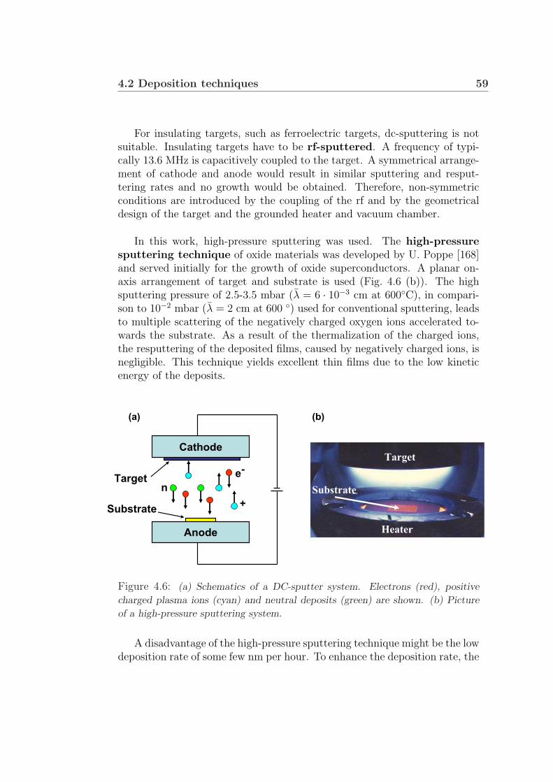
4.2 Deposition techniques 59
For insulating targets, such as ferroelectric targets, dc-sputtering is notsuitable. Insulating targets have to be rf-sputtered. A frequency of typi-cally 13.6 MHz is capacitively coupled to the target. A symmetrical arrange-ment of cathode and anode would result in similar sputtering and resput-tering rates and no growth would be obtained. Therefore, non-symmetricconditions are introduced by the coupling of the rf and by the geometricaldesign of the target and the grounded heater and vacuum chamber.
In this work, high-pressure sputtering was used. The high-pressuresputtering technique of oxide materials was developed by U. Poppe [168]and served initially for the growth of oxide superconductors. A planar on-axis arrangement of target and substrate is used (Fig. 4.6 (b)). The highsputtering pressure of 2.5-3.5 mbar (λ = 6 · 10−3 cm at 600C), in compari-son to 10−2 mbar (λ = 2 cm at 600 ) used for conventional sputtering, leadsto multiple scattering of the negatively charged oxygen ions accelerated to-wards the substrate. As a result of the thermalization of the charged ions,the resputtering of the deposited films, caused by negatively charged ions, isnegligible. This technique yields excellent thin films due to the low kineticenergy of the deposits.
Target
Substrate
Heater
(b)
Cathode
Anode
Substrate
Target e-
+
n
(a)
Figure 4.6: (a) Schematics of a DC-sputter system. Electrons (red), positive
charged plasma ions (cyan) and neutral deposits (green) are shown. (b) Picture
of a high-pressure sputtering system.
A disadvantage of the high-pressure sputtering technique might be the lowdeposition rate of some few nm per hour. To enhance the deposition rate, the

60 Heteroepitaxy of oxide perovskites
low ionization degree of less than 1 % of the atoms of a plasma is improvedby use of magnetic fields forcing the electron onto helical paths close to thecathode, resulting in a much higher ionization probability. This so-calledmagnetron sputtering can be used for high-pressure sputtering [169], aswell as for regular sputtering [170].
Chapter 5
Characterization techniques
The substantial progress in studying the ferroelectric limit has been achievednot only due to the advance in the understanding of boundary conditions, onthe one hand, and improvements in the deposition techniques, on the otherhand, but to a large extent on the capability of sophisticated analysis andcharacterization methods, too.
This Chapter provides a brief overview and description of the primarycharacterization tools used in this thesis. More information can be found inRefs. [171, 172, 173].
5.1 Structural characterization
Diffraction techniques are generally used to analyze the structural propertiesof crystals, powders and thin films. Different incident exciting probes, suchas photons, electrons, or neutrons having different energies, are used to studythe samples. This is partly due to the fact that in order to resolve the struc-tural characteristics of a sample, the wavelength of the probing beam has tobe in the same order of magnitude as the length scale of the structures underinvestigation. It is also partly due to the need of a strong interaction betweenprobe and sample. For instance, magnetic properties are best investigatedby neutrons, because of the strong interaction of magnetic fields with themagnetic moment of a neutron. The information is extracted from a changein energy, momentum, polarization or spin.
In this Chapter the most frequently used structural characterization tech-niques are presented.

62 Characterization techniques
X-ray diffraction
X-ray diffraction and reflectivity measurements provide information on thecrystal structure, layer thickness (details can be found in Ref. [172]), sur-face roughness or, in case of a multilayer, the multilayer period and interfacequality.
Within this work, studies of the crystallographic structure were performedby x-ray diffraction (XRD) measurements using a Philips X’pert MRD four-circle diffractometer with a copper x-ray tube (characteristic wavelength Cu-Kα1, λ = 0.15406 nm). For some few experiments a Picker four-circle diffrac-tometer was used. Fig. 5.1 shows a schematic of the four-circle geometry. Thedetector (angle 2θ) and the sample (angle θ or ω) can be rotated indepen-dently in the axis perpendicular to the scattering plane, which is defined bythe incident and diffracted beam. This enables probing of the crystallineplanes in a film parallel to the substrate surface. The φ and ψ circles allowprobing of reflections and planes that are not parallel to the surface of thesubstrate.
ϕ − scanIncident B
eam DiffractedBeam
θ θ
ω − scan ψ − scan
θ −2θ scan
Sample
x
z y
Figure 5.1: Simplified illustration of the four-circle x-ray diffractometry.
A x-ray beam1 that impinge on the sample surface under the angle of
1photons emitted by the anode of the x-ray tube with an energy characteristic for theanode material
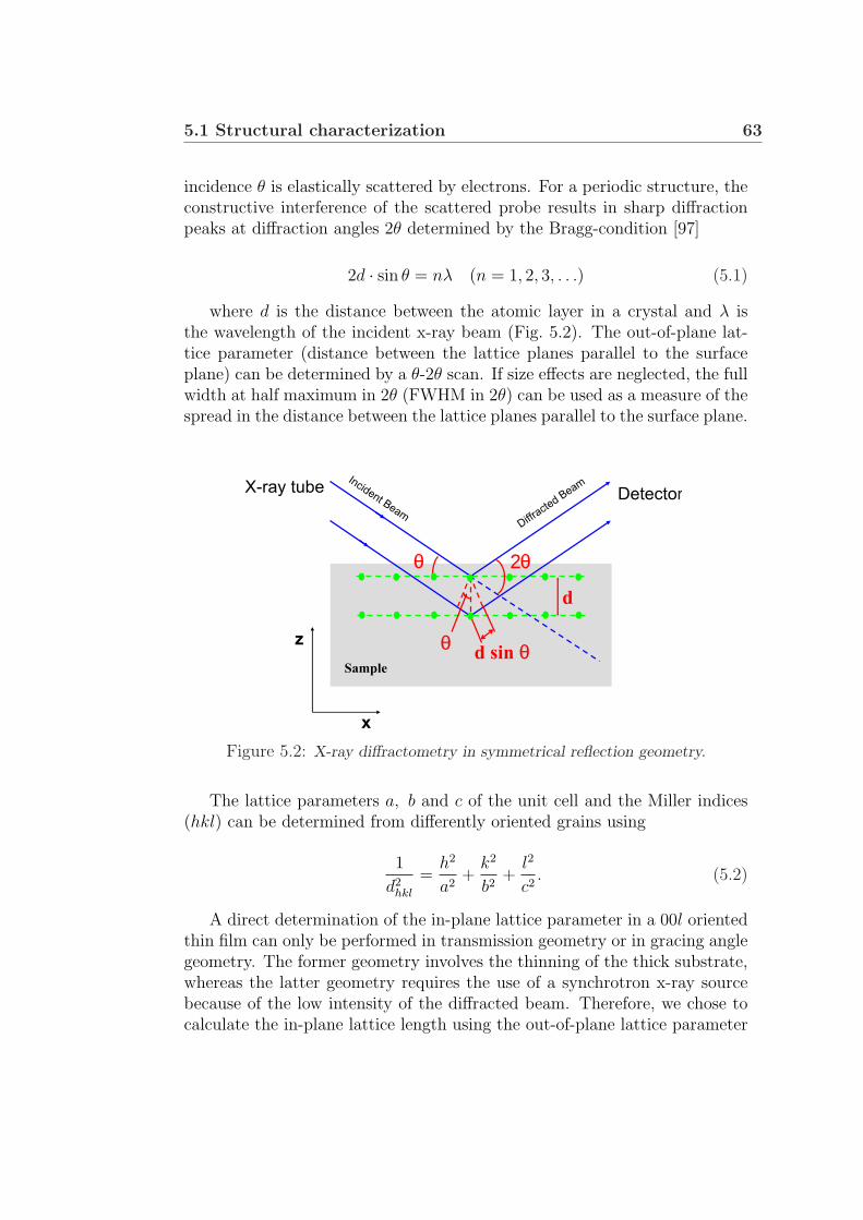
5.1 Structural characterization 63
incidence θ is elastically scattered by electrons. For a periodic structure, theconstructive interference of the scattered probe results in sharp diffractionpeaks at diffraction angles 2θ determined by the Bragg-condition [97]
2d · sin θ = nλ (n = 1, 2, 3, . . .) (5.1)
where d is the distance between the atomic layer in a crystal and λ isthe wavelength of the incident x-ray beam (Fig. 5.2). The out-of-plane lat-tice parameter (distance between the lattice planes parallel to the surfaceplane) can be determined by a θ-2θ scan. If size effects are neglected, the fullwidth at half maximum in 2θ (FWHM in 2θ) can be used as a measure of thespread in the distance between the lattice planes parallel to the surface plane.
θ
d
Sample
θd sin θ
2θ
X-ray tube Detector
x
z
Incident BeamDiffractedBeam
Figure 5.2: X-ray diffractometry in symmetrical reflection geometry.
The lattice parameters a, b and c of the unit cell and the Miller indices(hkl) can be determined from differently oriented grains using
1
d2hkl
=h2
a2+
k2
b2+
l2
c2. (5.2)
A direct determination of the in-plane lattice parameter in a 00l orientedthin film can only be performed in transmission geometry or in gracing anglegeometry. The former geometry involves the thinning of the thick substrate,whereas the latter geometry requires the use of a synchrotron x-ray sourcebecause of the low intensity of the diffracted beam. Therefore, we chose tocalculate the in-plane lattice length using the out-of-plane lattice parameter
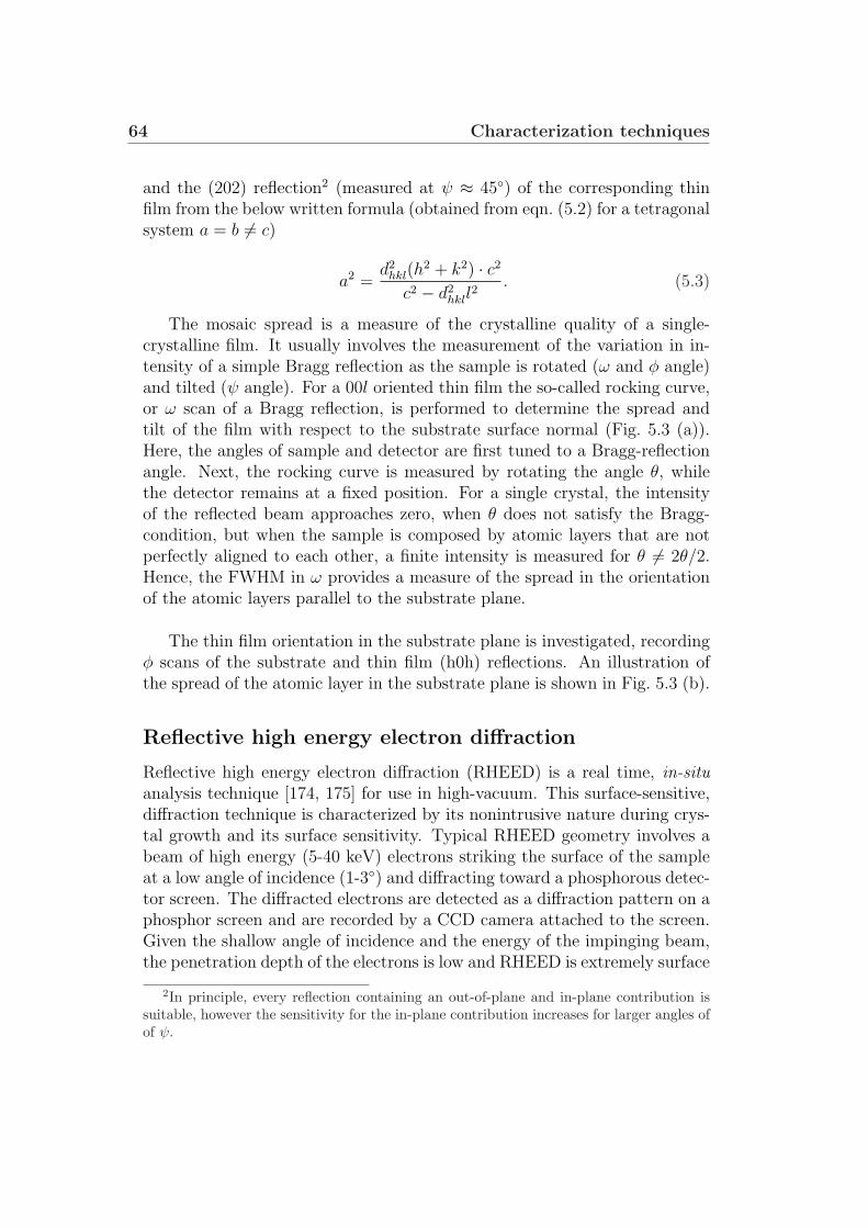
64 Characterization techniques
and the (202) reflection2 (measured at ψ ≈ 45) of the corresponding thinfilm from the below written formula (obtained from eqn. (5.2) for a tetragonalsystem a = b 6= c)
a2 =d2
hkl(h2 + k2) · c2
c2 − d2hkll
2. (5.3)
The mosaic spread is a measure of the crystalline quality of a single-crystalline film. It usually involves the measurement of the variation in in-tensity of a simple Bragg reflection as the sample is rotated (ω and φ angle)and tilted (ψ angle). For a 00l oriented thin film the so-called rocking curve,or ω scan of a Bragg reflection, is performed to determine the spread andtilt of the film with respect to the substrate surface normal (Fig. 5.3 (a)).Here, the angles of sample and detector are first tuned to a Bragg-reflectionangle. Next, the rocking curve is measured by rotating the angle θ, whilethe detector remains at a fixed position. For a single crystal, the intensityof the reflected beam approaches zero, when θ does not satisfy the Bragg-condition, but when the sample is composed by atomic layers that are notperfectly aligned to each other, a finite intensity is measured for θ 6= 2θ/2.Hence, the FWHM in ω provides a measure of the spread in the orientationof the atomic layers parallel to the substrate plane.
The thin film orientation in the substrate plane is investigated, recordingφ scans of the substrate and thin film (h0h) reflections. An illustration ofthe spread of the atomic layer in the substrate plane is shown in Fig. 5.3 (b).
Reflective high energy electron diffraction
Reflective high energy electron diffraction (RHEED) is a real time, in-situanalysis technique [174, 175] for use in high-vacuum. This surface-sensitive,diffraction technique is characterized by its nonintrusive nature during crys-tal growth and its surface sensitivity. Typical RHEED geometry involves abeam of high energy (5-40 keV) electrons striking the surface of the sampleat a low angle of incidence (1-3) and diffracting toward a phosphorous detec-tor screen. The diffracted electrons are detected as a diffraction pattern on aphosphor screen and are recorded by a CCD camera attached to the screen.Given the shallow angle of incidence and the energy of the impinging beam,the penetration depth of the electrons is low and RHEED is extremely surface
2In principle, every reflection containing an out-of-plane and in-plane contribution issuitable, however the sensitivity for the in-plane contribution increases for larger angles ofof ψ.
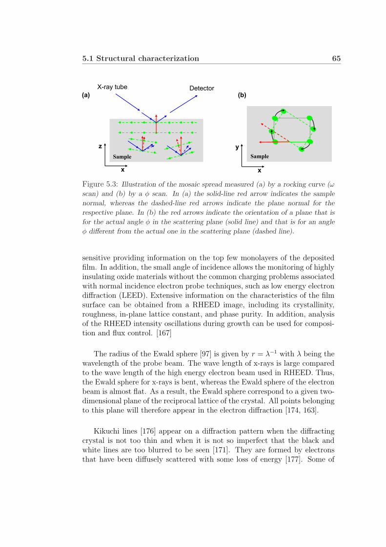
5.1 Structural characterization 65
x
y
SampleSample
X-ray tube Detector
x
z
(a) (b)
Figure 5.3: Illustration of the mosaic spread measured (a) by a rocking curve (ω
scan) and (b) by a φ scan. In (a) the solid-line red arrow indicates the sample
normal, whereas the dashed-line red arrows indicate the plane normal for the
respective plane. In (b) the red arrows indicate the orientation of a plane that is
for the actual angle φ in the scattering plane (solid line) and that is for an angle
φ different from the actual one in the scattering plane (dashed line).
sensitive providing information on the top few monolayers of the depositedfilm. In addition, the small angle of incidence allows the monitoring of highlyinsulating oxide materials without the common charging problems associatedwith normal incidence electron probe techniques, such as low energy electrondiffraction (LEED). Extensive information on the characteristics of the filmsurface can be obtained from a RHEED image, including its crystallinity,roughness, in-plane lattice constant, and phase purity. In addition, analysisof the RHEED intensity oscillations during growth can be used for composi-tion and flux control. [167]
The radius of the Ewald sphere [97] is given by r = λ−1 with λ being thewavelength of the probe beam. The wave length of x-rays is large comparedto the wave length of the high energy electron beam used in RHEED. Thus,the Ewald sphere for x-rays is bent, whereas the Ewald sphere of the electronbeam is almost flat. As a result, the Ewald sphere correspond to a given two-dimensional plane of the reciprocal lattice of the crystal. All points belongingto this plane will therefore appear in the electron diffraction [174, 163].
Kikuchi lines [176] appear on a diffraction pattern when the diffractingcrystal is not too thin and when it is not so imperfect that the black andwhite lines are too blurred to be seen [171]. They are formed by electronsthat have been diffusely scattered with some loss of energy [177]. Some of
66 Characterization techniques
these diffusely scattered electrons find themselves going in exactly the rightdirections to reflect from some planes in the crystal.
Rutherford backscattering spectrometry
Rutherford backscattering spectrometry (RBS) is a technique for determin-ing stoichiometry, layer thickness, interface quality and crystalline perfectionof a thin film.
In RBS, the sample is placed in front of a collimated beam of mono-energetic, low mass ions. For instance, within this work, the experimentswere performed with 1.4 MeV He+ ions. A small fraction of the ions thatimpinge on the sample are scattered back elastically by the nuclei of theatoms and are collected by a detector. The detector determines the energyof the backscattered ions, resulting in a energy spectrum - the so-called RBSspectrum.
In the random configuration (Fig. 5.4, left side) the sample is rotated toavoid the channeling of the He+ beam. The energy transferred from a He+
ion to the sample atom depends on the kinetic energy of incident ion andmass of the stationary sample atom. Energy loss, due to inelastic scatteringby the electronic structure of the sample atoms, occurs for He+ ions thatpenetrate deeper inside the sample. The energy of the ions collected in thedetector, thus, provides information about the mass of sample atoms and thethickness of layers. In addition, information about the interface sharpnessbetween two layers is obtained from the abruptness of the low energy edge ofthe energy interval for the respective sample atoms. Stoichiometry and layerthickness are obtained from the comparison of the so-called random spectrum(Fig. 5.4 (a)) with a simulation provided by the program RUMP [178].
The channeling spectrum is recorded without rotating the sample duringthe measurement (Fig. 5.4 (b)). Here, the sample is aligned to a low indexcrystal direction, allowing the beam to be guided by the atomic rows leadingto a reduction of the probability of being backscattered. Defects inside thefilm will lead to scattering out of the channeling direction and a fraction ofthese ions will be backscattered and collected by the detector. A measureof the crystalline perfection of the sample is, therefore, the minimum yieldχmin. This is the minimum in the intensity ratio of channeling and randomspectra.
5.1 Structural characterization 67
Θ
He+
Detector
Random Channeling
Figure 5.4: Illustration of Rutherford backscattering spectrometry. Random (left
side) and channeling (right side) experiments. [179]
Atomic force microscopy
Scanning probe microscopy (SPM) is a fast developing technique that allowsthe surface analysis of thin films and single crystals with atomic resolution. Afine tip scans the surface of the sample. The interaction between surface andtip depends on the physical properties of the surface being investigated. Alarge family of SPM-related techniques have been developed to study variousinteractions between tip and surface arising from different physical proper-ties. An overview can be found in Ref. [180].
The scanning probe technique used in this work is the atomic force mi-croscopy (AFM)3 illustrated in Fig. 5.5. Here, a sharp tip positioned at asmall distance from the sample scans the sample relative to the probing tip.The deflection of the cantilever as a function of lateral position is measuredby means of a reflected laser beam striking a 4-quadrant photodiode, and it issubsequently visualized in a 3-dimensional surface image. Different scanningmodes are used depending on sample properties and requested information.In the non-contact mode (distance between tip and sample surface greaterthan 1 nm), the tip-sample surface interactions involve van der Waals, elec-trostatic, magnetic or capillary forces. In the contact mode, ionic repulsionforces are dominant.
3AFM investigations presented in this work were performed by K. Szot, Forschungszen-
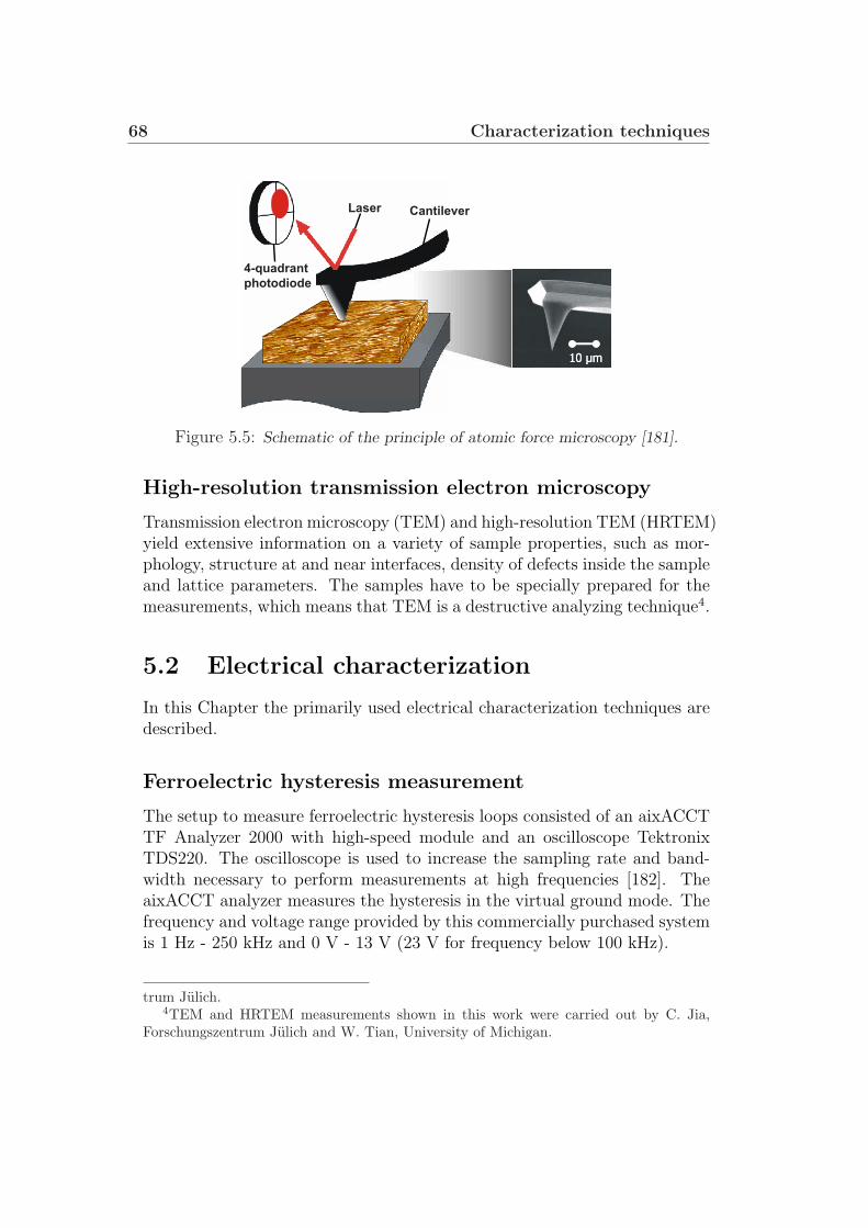
68 Characterization techniques
10 µm10 µm
4-quadrant
photodiode
Laser Cantilever
Figure 5.5: Schematic of the principle of atomic force microscopy [181].
High-resolution transmission electron microscopy
Transmission electron microscopy (TEM) and high-resolution TEM (HRTEM)yield extensive information on a variety of sample properties, such as mor-phology, structure at and near interfaces, density of defects inside the sampleand lattice parameters. The samples have to be specially prepared for themeasurements, which means that TEM is a destructive analyzing technique4.
5.2 Electrical characterization
In this Chapter the primarily used electrical characterization techniques aredescribed.
Ferroelectric hysteresis measurement
The setup to measure ferroelectric hysteresis loops consisted of an aixACCTTF Analyzer 2000 with high-speed module and an oscilloscope TektronixTDS220. The oscilloscope is used to increase the sampling rate and band-width necessary to perform measurements at high frequencies [182]. TheaixACCT analyzer measures the hysteresis in the virtual ground mode. Thefrequency and voltage range provided by this commercially purchased systemis 1 Hz - 250 kHz and 0 V - 13 V (23 V for frequency below 100 kHz).
trum Julich.4TEM and HRTEM measurements shown in this work were carried out by C. Jia,
Forschungszentrum Julich and W. Tian, University of Michigan.
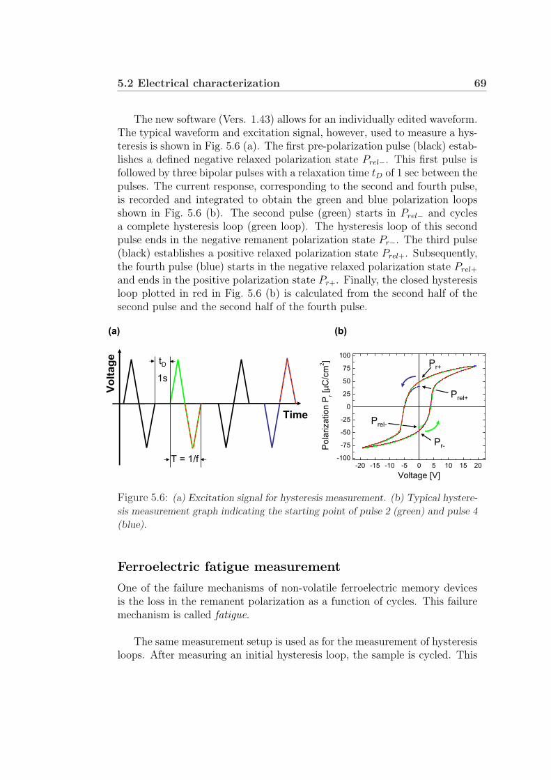
5.2 Electrical characterization 69
The new software (Vers. 1.43) allows for an individually edited waveform.The typical waveform and excitation signal, however, used to measure a hys-teresis is shown in Fig. 5.6 (a). The first pre-polarization pulse (black) estab-lishes a defined negative relaxed polarization state Prel−. This first pulse isfollowed by three bipolar pulses with a relaxation time tD of 1 sec between thepulses. The current response, corresponding to the second and fourth pulse,is recorded and integrated to obtain the green and blue polarization loopsshown in Fig. 5.6 (b). The second pulse (green) starts in Prel− and cyclesa complete hysteresis loop (green loop). The hysteresis loop of this secondpulse ends in the negative remanent polarization state Pr−. The third pulse(black) establishes a positive relaxed polarization state Prel+. Subsequently,the fourth pulse (blue) starts in the negative relaxed polarization state Prel+
and ends in the positive polarization state Pr+. Finally, the closed hysteresisloop plotted in red in Fig. 5.6 (b) is calculated from the second half of thesecond pulse and the second half of the fourth pulse.
Voltage
Time
T = 1/f
tD
1s
-20 -15 -10 -5 0 5 10 15 20-100
-75
-50
-25
0
25
50
75
100
Pola
rization P
r [µC
/cm
2]
Voltage [V]
(a) (b)
Pr-
Pr+
Prel-
Prel+
Figure 5.6: (a) Excitation signal for hysteresis measurement. (b) Typical hystere-
sis measurement graph indicating the starting point of pulse 2 (green) and pulse 4
(blue).
Ferroelectric fatigue measurement
One of the failure mechanisms of non-volatile ferroelectric memory devicesis the loss in the remanent polarization as a function of cycles. This failuremechanism is called fatigue.
The same measurement setup is used as for the measurement of hysteresisloops. After measuring an initial hysteresis loop, the sample is cycled. This
70 Characterization techniques
cycling involves permanent polarization reversals with a frequency and volt-age amplitude to be selected prior to measurement. The fatigue treatment isinterrupted regularly for hysteresis measurements. Usually the remanent (orrelaxed) polarization of the in between recorded hysteresis measurements isplotted as a function of the logarithm of the total number of fatigue cycles.
Current-voltage characteristic
I-V curves have been measured in a four-point arrangement to eliminatelead resistances. The fabrication process of the junctions will be describedin Chapter 8. Most measurements shown here, have been recorded usinga battery-powered current source. The voltage dependence of the dynamicconductance dI/dV was either simultaneously measured with a lock-in am-plifier, or it was calculated from the I-V characteristic. Measurements in atemperature range from 4.2 K to 300 K have been performed in a continuousflow cryostat.
Part II
Experimental results

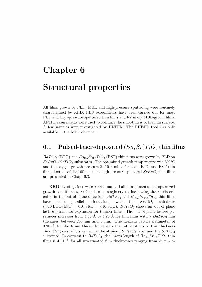
Chapter 6
Structural properties
All films grown by PLD, MBE and high-pressure sputtering were routinelycharacterized by XRD. RBS experiments have been carried out for mostPLD and high-pressure sputtered thin films and for many MBE-grown films.AFM measurements were used to optimize the smoothness of the film surface.A few samples were investigated by HRTEM. The RHEED tool was onlyavailable in the MBE chamber.
6.1 Pulsed-laser-deposited (Ba, Sr)TiO3 thin films
BaTiO3 (BTO) and Ba0.5Sr0.5TiO3 (BST) thin films were grown by PLD onSrRuO3/SrT iO3 substrates. The optimized growth temperature was 800Cand the oxygen growth pressure 2 · 10−3 mbar for both, BTO and BST thinfilms. Details of the 100 nm thick high-pressure sputtered SrRuO3 thin filmsare presented in Chap. 6.3.
XRD investigations were carried out and all films grown under optimizedgrowth conditions were found to be single-crystalline having the c-axis ori-ented in the out-of-plane direction. BaTiO3 and Ba0.5Sr0.5TiO3 thin filmshave exact parallel orientations with the SrT iO3 substrate([010]BTO/BST ‖ [010]SRO ‖ [010]STO). BaTiO3 shows an out-of-planelattice parameter expansion for thinner films. The out-of-plane lattice pa-rameter increases from 4.08 A to 4.20 A for thin films with a BaTiO3 filmthickness between 200 nm and 6 nm. The in-plane lattice parameter of3.90 A for the 6 nm thick film reveals that at least up to this thicknessBaTiO3 grows fully strained on the strained SrRuO3 layer and the SrT iO3
substrate. In contrast to BaTiO3, the c-axis length of Ba0.5Sr0.5TiO3 thinfilms is 4.01 A for all investigated film thicknesses ranging from 25 nm to
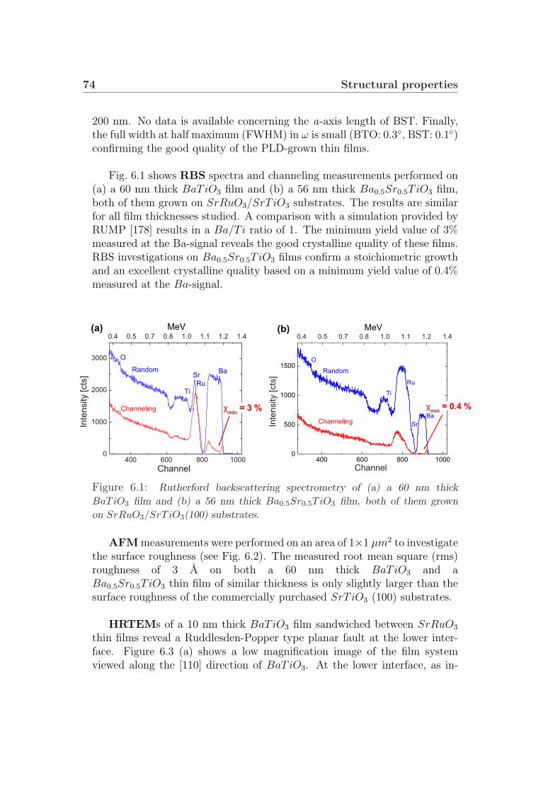
74 Structural properties
200 nm. No data is available concerning the a-axis length of BST. Finally,the full width at half maximum (FWHM) in ω is small (BTO: 0.3, BST: 0.1)confirming the good quality of the PLD-grown thin films.
Fig. 6.1 shows RBS spectra and channeling measurements performed on(a) a 60 nm thick BaTiO3 film and (b) a 56 nm thick Ba0.5Sr0.5TiO3 film,both of them grown on SrRuO3/SrT iO3 substrates. The results are similarfor all film thicknesses studied. A comparison with a simulation provided byRUMP [178] results in a Ba/T i ratio of 1. The minimum yield value of 3%measured at the Ba-signal reveals the good crystalline quality of these films.RBS investigations on Ba0.5Sr0.5TiO3 films confirm a stoichiometric growthand an excellent crystalline quality based on a minimum yield value of 0.4%measured at the Ba-signal.
400 600 800 10000
1000
2000
3000
Inte
nsity [cts
]
Channel
0.4 0.5 0.7 0.8 1.0 1.1 1.2 1.4
O
Ti
Sr
Ru
Ba
χmin
= 3 %
Random
Channeling
MeV
400 600 800 10000
500
1000
1500
Inte
nsity [cts
]
Channel
0.4 0.5 0.7 0.8 1.0 1.1 1.2 1.4
Sr
Ru
Ti
O
Ba
χmin
= 0.4 %
Random
Channeling
MeV(b)(a)
Figure 6.1: Rutherford backscattering spectrometry of (a) a 60 nm thick
BaTiO3 film and (b) a 56 nm thick Ba0.5Sr0.5TiO3 film, both of them grown
on SrRuO3/SrT iO3(100) substrates.
AFM measurements were performed on an area of 1×1 µm2 to investigatethe surface roughness (see Fig. 6.2). The measured root mean square (rms)roughness of 3 A on both a 60 nm thick BaTiO3 and aBa0.5Sr0.5TiO3 thin film of similar thickness is only slightly larger than thesurface roughness of the commercially purchased SrT iO3 (100) substrates.
HRTEMs of a 10 nm thick BaTiO3 film sandwiched between SrRuO3
thin films reveal a Ruddlesden-Popper type planar fault at the lower inter-face. Figure 6.3 (a) shows a low magnification image of the film systemviewed along the [110] direction of BaTiO3. At the lower interface, as in-
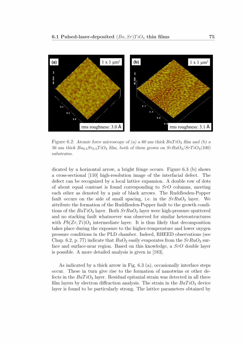
6.1 Pulsed-laser-deposited (Ba, Sr)TiO3 thin films 75
1 x 1 µm2 1 x 1 µm2
rms roughness: 3.0 Å rms roughness: 3.1 Å
(b)(a)
Figure 6.2: Atomic force microscopy of (a) a 60 nm thick BaTiO3 film and (b) a
56 nm thick Ba0.5Sr0.5TiO3 film, both of them grown on SrRuO3/SrT iO3(100)
substrates.
dicated by a horizontal arrow, a bright fringe occurs. Figure 6.3 (b) showsa cross-sectional [110] high-resolution image of the interfacial defect. Thedefect can be recognized by a local lattice expansion. A double row of dotsof about equal contrast is found corresponding to SrO columns, meetingeach other as denoted by a pair of black arrows. The Ruddlesden-Popperfault occurs on the side of small spacing, i.e. in the SrRuO3 layer. Weattribute the formation of the Ruddlesden-Popper fault to the growth condi-tions of the BaTiO3 layer. Both SrRuO3 layer were high-pressure sputteredand no stacking fault whatsoever was observed for similar heterostructureswith Pb(Zr, T i)O3 intermediate layer. It is thus likely that decompositiontakes place during the exposure to the higher-temperature and lower oxygenpressure conditions in the PLD chamber. Indeed, RHEED observations (seeChap. 6.2, p. 77) indicate that RuO2 easily evaporates from the SrRuO3 sur-face and surface-near region. Based on this knowledge, a SrO double layeris possible. A more detailed analysis is given in [183].
As indicated by a thick arrow in Fig. 6.3 (a), occasionally interface stepsoccur. These in turn give rise to the formation of nanotwins or other de-fects in the BaTiO3 layer. Residual epitaxial strain was detected in all threefilm layers by electron diffraction analysis. The strain in the BaTiO3 devicelayer is found to be particularly strong. The lattice parameters obtained by
76 Structural properties
BaTiO3
SrRuO3
(b)
[110]
BaTiO3
SrRuO3
SrRuO310 nm
(a)
Figure 6.3: High-resolution TEM of a 10 nm thick BaTiO3 film sandwiched
between SrRuO3 thin films grown on a SrT iO3(100) substrate. [183]
HRTEM are consistent with the data obtained by XRD. While no misfit dis-locations were found in the lower interface area, dislocations were observedin the upper part of the BaTiO3 layer giving rise to a partial relaxation ofthe BaTiO3 thin film.
A strain-induced shift of the paraelectric to ferroelectric phase transitiontemperature resulting from a two-dimensional clamping of the substrate willbe demonstrated using pulsed-laser-ablated BST thin films in Chap. 7.2,p. 106. The thickness dependence of ferroelectric properties for PLD-grownBTO films will be studied in Chap. 7.3, p. 108. In addition, the electricalcharacterization of ultrathin BTO films with a film thickness of 6 nm will bediscussed in Chapter 8.
6.2 Molecular beam epitaxy of SrRuO3 and
BaTiO3 thin films
Single crystalline SrRuO3 and BaTiO3 thin films were grown by MBE onSrT iO3 (100) substrates. All SrRuO3 thin films were grown 100 nm thick.The thickness of BaTiO3 thin films varied between 2 nm and 100 nm. TheSrT iO3 substrates were etched prior to deposition based on the proceduredeveloped by Masashi Kawasaki [184] and modified by Ivan Bozovic [185].The etch procedure yields smooth TiO2-terminated SrT iO3 surfaces. In ad-dition, SrRuO3 thin films were grown on lattice-matched DyScO3.
The growth of SrRuO3 was particularly challenging. Due to the highevaporation temperature of Ruthenium, e-beam evaporation was used. The

6.2 Molecular beam epitaxy of SrRuO3 and BaTiO3 thin films 77
ruthenium flux demonstrated significant drift during deposition. Neverthe-less, a successful growth of SrRuO3 was possible because Ru or RuO2 evap-orates easily from the sample surface [186, 187, 188]. By growing SrRuO3
using a layer-by-layer technique with a slight Ru-excess flux, a stoichiometricgrowth was achieved. Specific features in the RHEED pattern were used toidentify large Ru-excess. The Ru-flux could be adjusted during the deposi-tion by modifying the opening time of the Ru shutter, the e-beam currentand by manually adjusting the e-beam spot (see Fig. 6.4).
100 200 300
100
120
140
160
Inte
nsity [a.u
.]
Time [sec]
Sr
O
Ti
Ru
RuO2-depositionSrO-deposition
200 300
60
80
100
120
140
Inte
nsity [a.u
.]
Time [sec]
decreasing Ru-fluxincreased
e-beam current
(a) (b)
Figure 6.4: RHEED oscillations monitoring the specular spot of the [100] azimuth.
(a) Stable Ru-flux, (b) unstable Ru-flux. The sketch in the center schematically
shows the SrRuO3/SrT iO3 heterostructure.
MBE-grown SrRuO3 on SrT iO3 substrates
SrRuO3 thin films grown fully strained on SrT iO3 (100) substrates adopttheir a-axis lattice parameter of 3.895 A. If in first approximation a constantcell volume is assumed, a c-axis length of 3.95 A is expected. A signifi-cantly larger c-axis resulting in a larger cell volume is indicative of non-stoichiometry or the introduction of defects. The XRD measurements showthat the expected out-of-plane lattice parameter is reached only for the high-est investigated growth pressure of 5×10⁻⁶ torr1 in an O2/(10%)O3 mixture.
1All growth pressures used for the growth by MBE are given in torr, as this was thepressure unit used at PennState University. Nevertheless, the author is aware of the factthat torr is not a SI unit. To calculate the growth pressure in mbar the following relationis useful: 1000 mbar = 760 torr.
78 Structural properties
The growth pressure and growth temperature were limited due to limitationsof the heater that was used, and the threat of oxidizing the sources insidethe chamber. An annealing of the samples after growth did not show anyimprovement, i.e. a smaller c-axis length. As can be seen from Fig. 6.5 (a),at a given growth pressure the c-axis lattice parameter gets closer to the de-sired value when ozone (10 %) is added to oxygen (solid blue line). A lowergrowth temperature also decreases the c-axis length, however, at the sametime the full width at half maximum (FWHM) in ω increases (red lines). At agiven growth temperature the c-axis length decreases for higher growth pres-sures, but at the same time again the FWHM in ω increases (see Fig. 6.5 (b)).
575 600
3,96
3,97
3,98
3,99
4,00
4,01
c-a
xis
[Å]
Temperature [°C]
0,30
0,35
0,40
Resolution limit in ω
FW
HM
in ω
[°]
0,0 2,0x10⁻⁶
4,0x10⁻⁶
3,96
3,97
3,98
3,99
4,00
4,01
4,02
Resolution Limit in ω
c-a
xis
[Å]
O2/O
3 Growth Pressure [Torr]
0,30
0,35
0,40
0,45
FW
HM
in ω
[°]
(a) (b)
Figure 6.5: Results from XRD measurements on MBE-grown SrRuO3 thin films.
In (a) the temperature dependence for the growth in pure O2 (dashed line) and in
an O2/O3 mixture (solid line) at a growth pressure of 1 × 10⁻⁶ torr is shown. In
(b) the O2/O3 mixture growth pressure dependence of the c-axis length and the
FWHM in ω at 605C. Note that these XRD measurements were performed with
a Picker four-circle diffractometer with a resolution limit in ω of 0.3.
These results demonstrate the need for growth in an O2/O3 mixture ata growth pressure and temperature above the range investigated here in orderto grow fully strained (and defect-free) SrRuO3 thin films onSrT iO3 (100) substrates with an out-of-plane lattice parameter of 3.95 A anda low FWHM in ω.
The RHEED patterns shown in Fig. 6.6 confirm the increasing crys-talline quality of the MBE-grown SrRuO3 thin films for higher growth pres-sures. All pictures were taken after the growth of 100 nm thick films. TheO2/O3 mixture growth pressure increases from the left to the right starting at7×10−7 torr and ending at 5×10⁻⁶ torr. All thin films were grown at 605C.

6.2 Molecular beam epitaxy of SrRuO3 and BaTiO3 thin films 79
7 x 10⁻⁷ Torr 1 x 10⁻⁶ Torr 3 x 10⁻⁶ Torr 5 x 10⁻⁶ Torr
[100]
[110]
Figure 6.6: RHEED patterns of 100 nm thick SrRuO3 films grown by MBE at
605C in an O2/O3 mixture. The upper and lower patterns show the [100] and
[110] azimuth patterns, respectively.
RBS channeling experiments are consistent with XRD and RHEED re-sults. The minimum yield χmin decreases from 13% at growth pressures of7× 10−7 torr to 2.5% at 5× 10⁻⁶ torr (Fig. 6.7).
AFM measurements demonstrate that SrRuO3 thin films grown at sta-ble Ru-flux have smooth surfaces. Fig. 6.8 shows a 3-dimensional illustrationof the surface of a 100 nm thick SrRuO3 film. The root mean square rough-ness is only 2.4 A on an area of 5× 5 µm2 in size.
The metallic behavior of the temperature dependence of the resistivityis shown in Fig. 6.9 for various growth pressures. The resistivity decreasesfor higher O2/O3 pressures. The best value of 450 µC/cm2 at room temper-ature is obtained for the highest growth pressure of 5 × 10⁻⁶ torr. A kinkin the ρ(T )-curve is observable at the ferromagnetic-to-paramagnetic phasetransition. The phase transition occurs at about 142 K for the film grown at5× 10−6 torr. This smaller value compared to bulk (see Chap. 4.1) could bedue to a Ru-deficiency [187].
MBE-grown SrRuO3 on lattice-matched DyScO3
DyScO3 is a novel substrate made by IKZ (Institut fur Kristallzuchtung,Berlin). We report on the first results on SrRuO3 thin films grown on
80 Structural properties
400 600 800 10000
500
1000
1500
2000
Inte
nsity [cts
]
Channel
0,4 0,5 0,7 0,8 1,0 1,1 1,2 1,4
χmin
= 13 %
Random
Channeling
MeV
400 600 800 10000
500
1000
1500
2000
Inte
nsity [cts
]
Channel
0,4 0,5 0,7 0,8 1,0 1,1 1,2 1,4
χmin
= 3.5 %
Random
Channeling
MeV
400 600 800 10000
500
1000
1500
2000
Inte
nsity [cts
]
Channel
0,4 0,5 0,7 0,8 1,0 1,1 1,2 1,4
χmin
= 3.5 %
Random
Channeling
MeV
p02/03= 7 x 10⁻⁷ Torr
400 600 800 10000
500
1000
1500
2000
Inte
nsity [cts
]
Channel
0,4 0,5 0,7 0,8 1,0 1,1 1,2 1,4
χmin
= 2.5 %
Random
Channeling
MeV
p02/03= 1 x 10⁻⁶ Torr
p02/03= 3 x 10⁻⁶ Torr
p02/03= 5 x 10⁻⁶ Torr
Figure 6.7: RBS random and channeling experiments of 100 nm thick SrRuO3
films grown by MBE at several growth pressures at 605C in an O2/O3 mixture.
DyScO3 substrates. SrRuO3 thin films were grown at 605C and 3×10⁻⁶ torrin an O2/O3 mixture.
SrRuO3 grown on DyScO3 substrate is an almost perfectly lattice-matched heterostructure. Their pseudo-cubic lattice constants are 3.93 A and3.94 A, respectively. DyScO3 does not undergo a phase transition between1000C and room temperature and was found to have a similar thermalexpansion to other oxide perovskites (e.g. BaTiO3, SrRuO3 or SrT iO3),with an average thermal expansion of 8.4 ppm/C [189]. The idea is to growBaTiO3 thin films on SrRuO3/DyScO3. The smaller lattice mismatch of thisheterostructure compared to BaTiO3 thin films grown on SrRuO3/SrT iO3
substrates should introduce less misfit-strain in the BaTiO3 thin films. Thecritical film thickness for strain-relief via introduction of misfit dislocations
6.2 Molecular beam epitaxy of SrRuO3 and BaTiO3 thin films 81
Figure 6.8: 3-dimensional AFM illustration of a 100 nm thick SrRuO3 film grown
by MBE. The root mean square roughness is 1.8 A and 2.4 A on areas 1× 1 µm2
and 5× 5 µm2 in size, respectively.
will be shifted to thicker films. As a result, the growth of thicker, fullystrained and dislocation-free BaTiO3 thin films should be achievable.
XRD measurements confirm the excellent lattice match between SrRuO3
and DyScO3. Fig. 6.10 (a) shows a theta-2theta scan. No peak separationfor SrRuO3 and DyScO3 was observed for the pseudo-cubic [150] (001),(002) and (003) reflexes. A magnification of the pseudo-cubic (004) reflexesis shown in Fig. 6.10 (b). Here, four peaks are visible corresponding to theKα1 and Kα2 reflexes of SrRuO3 and DyScO3. These reflexes correspondto out-of-plane lattice parameters of 3.937 A and 3.945 A. The higher inten-
0 100 200 300
200
300
400
500
600
pO
2/O
3
= 7 x 10⁻⁷ Torr
pO
2/O
3
= 1 x 10⁻⁶ Torr
pO
2/O
3
= 3 x 10⁻⁶ Torr
pO
2/O
3
= 5 x 10⁻⁶ Torr
Resis
tivity ρ
[µ
Ωcm
]
Temperature [K]
IncresingpO2 /O3
Figure 6.9: Growth pressure dependence of the resistivity for 100 nm thick
SrRuO3 films grown by MBE at 605C for several growth pressures in an O2/O3
mixture.
82 Structural properties
sity suggests the former length to correspond to the much thicker DyScO3
substrate and the latter to the MBE-grown SrRuO3 thin film. The FWHMin ω (Fig. 6.10 (c)) for both materials is below 0.05, which is the resolutionlimit of the x-ray diffractometer that was used.
Fig. 6.11 shows the RHEED patterns for various azimuths (in orthorhom-bic and pseudo-cubic notation) of the as-delivered DyScO3 substrate.
The RHEED patterns of the [100] azimuth (in pseudo-cubic notation)before, during and after growth are shown in Fig. 6.12. In addition, a pictureof the pseudo-cubic [110] azimuth taken after growth is included. The niceRHEED pattern after growth including Kikuchi lines indicate an excellentcrystalline quality and a smooth surface.
20 40 60 80 10010
1
102
103
104
Inte
nsity [
cts
]
2-Theta [degrees]
100 101 102 103 104 105 106 10710
1
102
103
104
SrRuO3 (004)
pseudo
DyScO3 (004)
pseudo
Inte
nsity [cts
]
2-Theta [degrees]51,5 52,0
101
102
103
SrR
uO
3 (
004) p
se
ud
o
DyS
cO
3 (
004) p
se
ud
o
Inte
nsity [cts
]
Theta [degrees]
(a)
(b) (c)
Figure 6.10: XRD measurements of a 100 nm thick SrRuO3 film grown by MBE
on a DyScO3 substrate. (a) A theta-2theta scan, including (b) a magnification of
the pseudo-cubic (004) peaks and (c) the rocking curves for the separated peaks
shown in (b) are displayed.
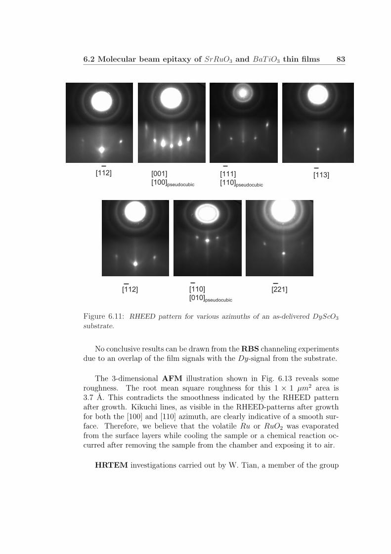
6.2 Molecular beam epitaxy of SrRuO3 and BaTiO3 thin films 83
[001]
[100]pseudocubic
[112]
[112] [110]
[010]pseudocubic
[221]
[111]
[110]pseudocubic
[113]
Figure 6.11: RHEED pattern for various azimuths of an as-delivered DyScO3
substrate.
No conclusive results can be drawn from the RBS channeling experimentsdue to an overlap of the film signals with the Dy-signal from the substrate.
The 3-dimensional AFM illustration shown in Fig. 6.13 reveals someroughness. The root mean square roughness for this 1 × 1 µm2 area is3.7 A. This contradicts the smoothness indicated by the RHEED patternafter growth. Kikuchi lines, as visible in the RHEED-patterns after growthfor both the [100] and [110] azimuth, are clearly indicative of a smooth sur-face. Therefore, we believe that the volatile Ru or RuO2 was evaporatedfrom the surface layers while cooling the sample or a chemical reaction oc-curred after removing the sample from the chamber and exposing it to air.
HRTEM investigations carried out by W. Tian, a member of the group
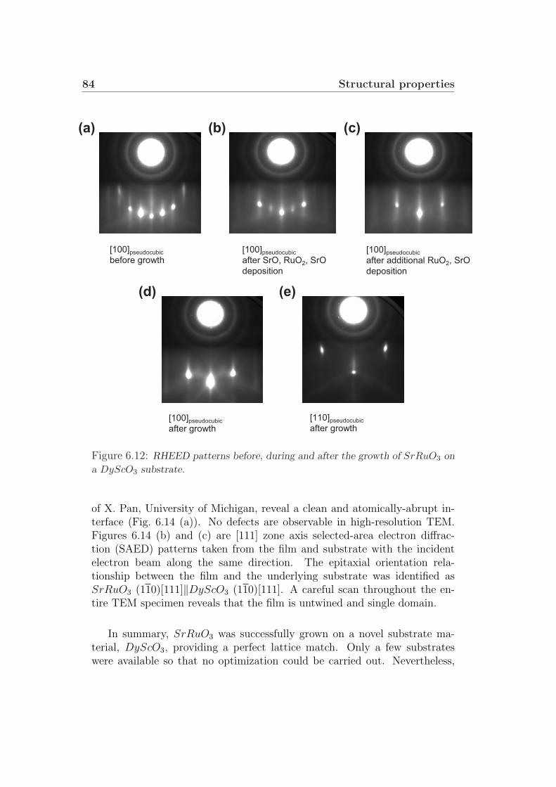
84 Structural properties
[100]pseudocubic
before growth
[100]pseudocubic
after SrO, RuO2, SrO
deposition
[100]pseudocubic
after additional RuO2, SrO
deposition
[100]pseudocubic
after growth
[110]pseudocubic
after growth
(a) (b) (c)
(d) (e)
Figure 6.12: RHEED patterns before, during and after the growth of SrRuO3 on
a DyScO3 substrate.
of X. Pan, University of Michigan, reveal a clean and atomically-abrupt in-terface (Fig. 6.14 (a)). No defects are observable in high-resolution TEM.Figures 6.14 (b) and (c) are [111] zone axis selected-area electron diffrac-tion (SAED) patterns taken from the film and substrate with the incidentelectron beam along the same direction. The epitaxial orientation rela-tionship between the film and the underlying substrate was identified asSrRuO3 (110)[111]‖DyScO3 (110)[111]. A careful scan throughout the en-tire TEM specimen reveals that the film is untwined and single domain.
In summary, SrRuO3 was successfully grown on a novel substrate ma-terial, DyScO3, providing a perfect lattice match. Only a few substrateswere available so that no optimization could be carried out. Nevertheless,
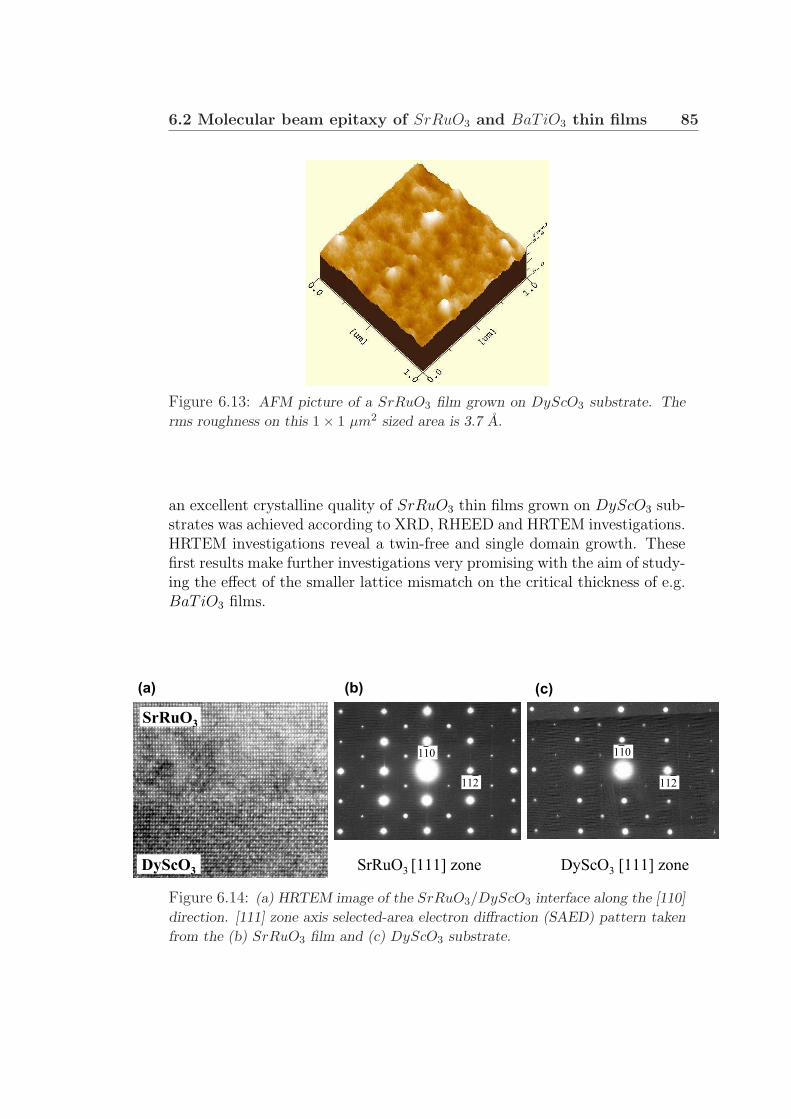
6.2 Molecular beam epitaxy of SrRuO3 and BaTiO3 thin films 85
Figure 6.13: AFM picture of a SrRuO3 film grown on DyScO3 substrate. The
rms roughness on this 1× 1 µm2 sized area is 3.7 A.
an excellent crystalline quality of SrRuO3 thin films grown on DyScO3 sub-strates was achieved according to XRD, RHEED and HRTEM investigations.HRTEM investigations reveal a twin-free and single domain growth. Thesefirst results make further investigations very promising with the aim of study-ing the effect of the smaller lattice mismatch on the critical thickness of e.g.BaTiO3 films.
DyScO3
SrRuO3
SrRuO3 [111] zone DyScO3 [111] zone
110
112
110
112
(a) (b) (c)
Figure 6.14: (a) HRTEM image of the SrRuO3/DyScO3 interface along the [110]
direction. [111] zone axis selected-area electron diffraction (SAED) pattern taken
from the (b) SrRuO3 film and (c) DyScO3 substrate.
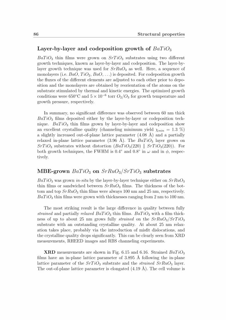
86 Structural properties
Layer-by-layer and codeposition growth of BaTiO3
BaTiO3 thin films were grown on SrT iO3 substrates using two differentgrowth techniques, known as layer-by-layer and codeposition. The layer-by-layer growth technique was used for SrRuO3 as well. Here, a sequence ofmonolayers (i.e. BaO, TiO2, BaO, . . .) is deposited. For codeposition growththe fluxes of the different elements are adjusted to each other prior to depo-sition and the monolayers are obtained by reorientation of the atoms on thesubstrate stimulated by thermal and kinetic energies. The optimized growthconditions were 650C and 5× 10⁻⁶ torr O2/O3 for growth temperature andgrowth pressure, respectively.
In summary, no significant difference was observed between 60 nm thickBaTiO3 films deposited either by the layer-by-layer or codeposition tech-nique. BaTiO3 thin films grown by layer-by-layer and codeposition showan excellent crystalline quality (channeling minimum yield χmin = 1.3 %)a slightly increased out-of-plane lattice parameter (4.08 A) and a partiallyrelaxed in-plane lattice parameter (3.96 A). The BaTiO3 layer grows onSrT iO3 substrates without distortion (BaTiO3(220) ‖ SrT iO3(220)). Forboth growth techniques, the FWHM is 0.4 and 0.8 in ω and in φ, respec-tively.
MBE-grown BaTiO3 on SrRuO3/SrT iO3 substrates
BaTiO3 was grown in-situ by the layer-by-layer technique either on SrRuO3
thin films or sandwiched between SrRuO3 films. The thickness of the bot-tom and top SrRuO3 thin films were always 100 nm and 25 nm, respectively.BaTiO3 thin films were grown with thicknesses ranging from 2 nm to 100 nm.
The most striking result is the large difference in quality between fullystrained and partially relaxed BaTiO3 thin films. BaTiO3 with a film thick-ness of up to about 25 nm grows fully strained on the SrRuO3/SrT iO3
substrate with an outstanding crystalline quality. At about 25 nm relax-ation takes place, probably via the introduction of misfit dislocations, andthe crystalline quality drops significantly. This can be clearly seen from XRDmeasurements, RHEED images and RBS channeling experiments.
XRD measurements are shown in Fig. 6.15 and 6.16. Strained BaTiO3
films have an in-plane lattice parameter of 3.895 A following the in-planelattice parameter of the SrT iO3 substrate and the strained SrRuO3 layer.The out-of-plane lattice parameter is elongated (4.19 A). The cell volume is
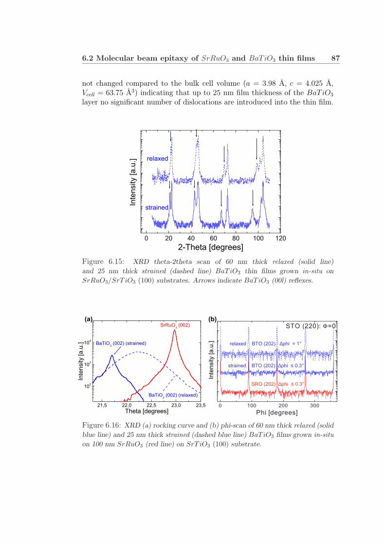
6.2 Molecular beam epitaxy of SrRuO3 and BaTiO3 thin films 87
not changed compared to the bulk cell volume (a = 3.98 A, c = 4.025 A,Vcell = 63.75 A3) indicating that up to 25 nm film thickness of the BaTiO3
layer no significant number of dislocations are introduced into the thin film.
0 20 40 60 80 100 120
strained
relaxed
2-Theta [degrees]
Inte
nsity
[a.u
.]
Figure 6.15: XRD theta-2theta scan of 60 nm thick relaxed (solid line)
and 25 nm thick strained (dashed line) BaTiO3 thin films grown in-situ on
SrRuO3/SrT iO3 (100) substrates. Arrows indicate BaTiO3 (00l) reflexes.
0 100 200 300
STO (220): Φ=0
Phi [degrees]
strained BTO (202) ∆phi 0.3°
relaxed BTO (202) ∆phi = 1°
Inte
nsity
[a.u
.]
SRO (202) ∆phi 0.3°
(b)
21,5 22,0 22,5 23,0 23,5
102
103
104
BaTiO3 (002) (strained)
BaTiO3 (002) (relaxed)
SrRuO3 (002)
Inte
nsity [a.u
.]
Theta [degrees]
(a)
Figure 6.16: XRD (a) rocking curve and (b) phi-scan of 60 nm thick relaxed (solid
blue line) and 25 nm thick strained (dashed blue line) BaTiO3 films grown in-situon 100 nm SrRuO3 (red line) on SrT iO3 (100) substrate.
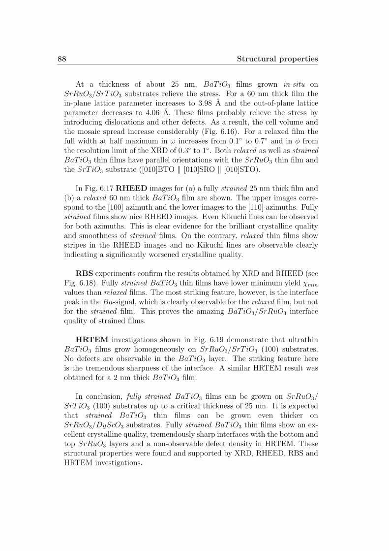
88 Structural properties
At a thickness of about 25 nm, BaTiO3 films grown in-situ onSrRuO3/SrT iO3 substrates relieve the stress. For a 60 nm thick film thein-plane lattice parameter increases to 3.98 A and the out-of-plane latticeparameter decreases to 4.06 A. These films probably relieve the stress byintroducing dislocations and other defects. As a result, the cell volume andthe mosaic spread increase considerably (Fig. 6.16). For a relaxed film thefull width at half maximum in ω increases from 0.1 to 0.7 and in φ fromthe resolution limit of the XRD of 0.3 to 1. Both relaxed as well as strainedBaTiO3 thin films have parallel orientations with the SrRuO3 thin film andthe SrT iO3 substrate ([010]BTO ‖ [010]SRO ‖ [010]STO).
In Fig. 6.17 RHEED images for (a) a fully strained 25 nm thick film and(b) a relaxed 60 nm thick BaTiO3 film are shown. The upper images corre-spond to the [100] azimuth and the lower images to the [110] azimuths. Fullystrained films show nice RHEED images. Even Kikuchi lines can be observedfor both azimuths. This is clear evidence for the brilliant crystalline qualityand smoothness of strained films. On the contrary, relaxed thin films showstripes in the RHEED images and no Kikuchi lines are observable clearlyindicating a significantly worsened crystalline quality.
RBS experiments confirm the results obtained by XRD and RHEED (seeFig. 6.18). Fully strained BaTiO3 thin films have lower minimum yield χmin
values than relaxed films. The most striking feature, however, is the interfacepeak in the Ba-signal, which is clearly observable for the relaxed film, but notfor the strained film. This proves the amazing BaTiO3/SrRuO3 interfacequality of strained films.
HRTEM investigations shown in Fig. 6.19 demonstrate that ultrathinBaTiO3 films grow homogeneously on SrRuO3/SrT iO3 (100) substrates.No defects are observable in the BaTiO3 layer. The striking feature hereis the tremendous sharpness of the interface. A similar HRTEM result wasobtained for a 2 nm thick BaTiO3 film.
In conclusion, fully strained BaTiO3 films can be grown on SrRuO3/SrT iO3 (100) substrates up to a critical thickness of 25 nm. It is expectedthat strained BaTiO3 thin films can be grown even thicker onSrRuO3/DyScO3 substrates. Fully strained BaTiO3 thin films show an ex-cellent crystalline quality, tremendously sharp interfaces with the bottom andtop SrRuO3 layers and a non-observable defect density in HRTEM. Thesestructural properties were found and supported by XRD, RHEED, RBS andHRTEM investigations.
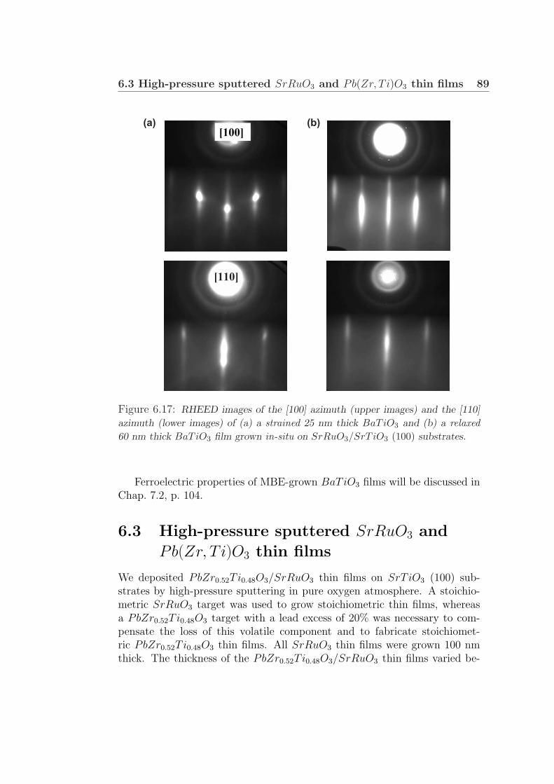
6.3 High-pressure sputtered SrRuO3 and Pb(Zr, T i)O3 thin films 89
[100]
[110]
(a) (b)
Figure 6.17: RHEED images of the [100] azimuth (upper images) and the [110]
azimuth (lower images) of (a) a strained 25 nm thick BaTiO3 and (b) a relaxed60 nm thick BaTiO3 film grown in-situ on SrRuO3/SrT iO3 (100) substrates.
Ferroelectric properties of MBE-grown BaTiO3 films will be discussed inChap. 7.2, p. 104.
6.3 High-pressure sputtered SrRuO3 and
Pb(Zr, T i)O3 thin films
We deposited PbZr0.52Ti0.48O3/SrRuO3 thin films on SrT iO3 (100) sub-strates by high-pressure sputtering in pure oxygen atmosphere. A stoichio-metric SrRuO3 target was used to grow stoichiometric thin films, whereasa PbZr0.52Ti0.48O3 target with a lead excess of 20% was necessary to com-pensate the loss of this volatile component and to fabricate stoichiomet-ric PbZr0.52Ti0.48O3 thin films. All SrRuO3 thin films were grown 100 nmthick. The thickness of the PbZr0.52Ti0.48O3/SrRuO3 thin films varied be-
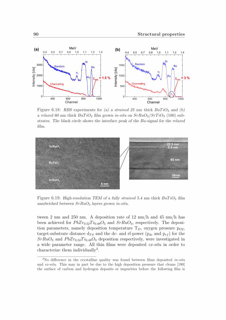
90 Structural properties
400 600 800 10000
500
1000
1500
Ti
Sr
Ru
Ba
Inte
nsity [cts
]
Channel
0,4 0,5 0,7 0,8 1,0 1,1 1,2 1,4
χmin
= 3 %
Random
Channeling
MeV
400 600 800 10000
1000
2000
3000
Inte
nsity [cts
]
Channel
0,4 0,5 0,7 0,8 1,0 1,1 1,2 1,4
Ti
Sr
Ru
Ba
χmin
= 1.5 %
Random
Channeling
MeV(a) (b)
Figure 6.18: RBS experiments for (a) a strained 25 nm thick BaTiO3 and (b)
a relaxed 60 nm thick BaTiO3 film grown in-situ on SrRuO3/SrT iO3 (100) sub-
strates. The black circle shows the interface peak of the Ba-signal for the relaxedfilm.
30nm
22.5 nm
5.4 nm
95 nm
SrRuO3
SrRuO3
BaTiO3
4 nm
Figure 6.19: High-resolution TEM of a fully strained 5.4 nm thick BaTiO3 film
sandwiched between SrRuO3 layers grown in-situ.
tween 2 nm and 250 nm. A deposition rate of 12 nm/h and 45 nm/h hasbeen achieved for PbZr0.52Ti0.48O3 and SrRuO3, respectively. The deposi-tion parameters, namely deposition temperature TD, oxygen pressure pO2,target-substrate distance dTS and the dc- and rf-power (pdc and prf ) for theSrRuO3 and PbZr0.52Ti0.48O3 deposition respectively, were investigated ina wide parameter range. All thin films were deposited ex-situ in order tocharacterize them individually2.
2No difference in the crystalline quality was found between films deposited in-situand ex-situ. This may in part be due to the high deposition pressure that cleans [190]the surface of carbon and hydrogen deposits or impurities before the following film is
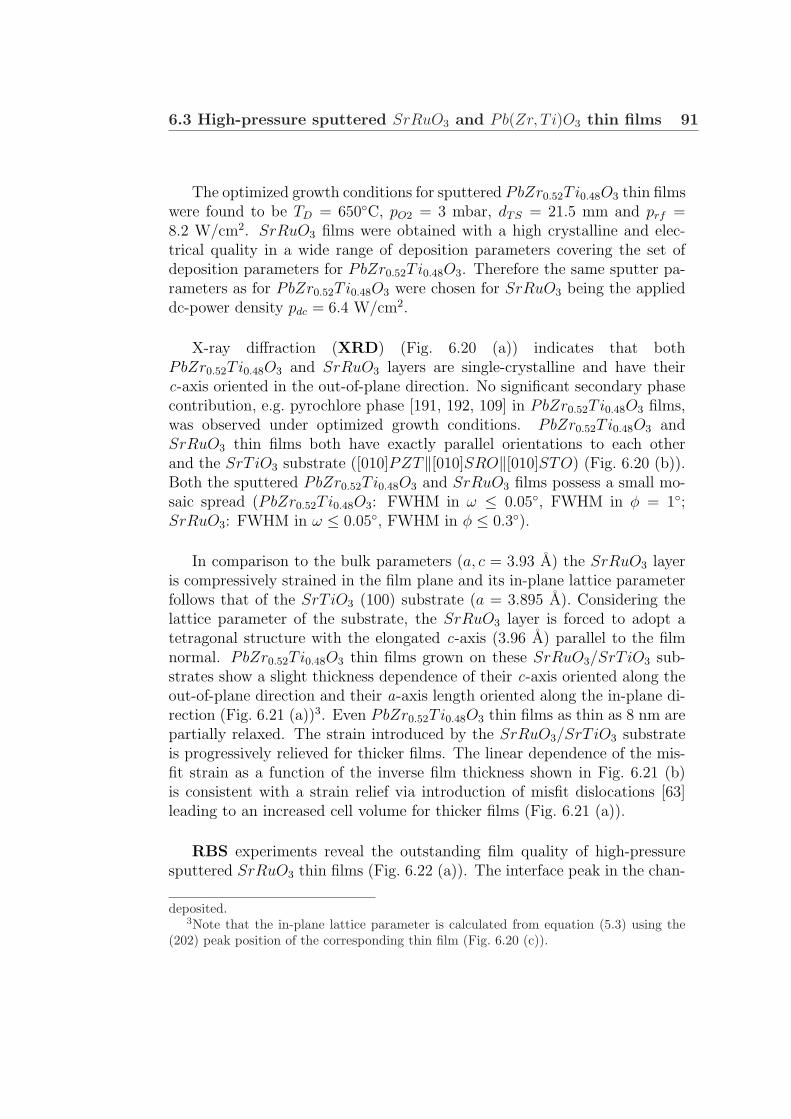
6.3 High-pressure sputtered SrRuO3 and Pb(Zr, T i)O3 thin films 91
The optimized growth conditions for sputtered PbZr0.52Ti0.48O3 thin filmswere found to be TD = 650C, pO2 = 3 mbar, dTS = 21.5 mm and prf =8.2 W/cm2. SrRuO3 films were obtained with a high crystalline and elec-trical quality in a wide range of deposition parameters covering the set ofdeposition parameters for PbZr0.52Ti0.48O3. Therefore the same sputter pa-rameters as for PbZr0.52Ti0.48O3 were chosen for SrRuO3 being the applieddc-power density pdc = 6.4 W/cm2.
X-ray diffraction (XRD) (Fig. 6.20 (a)) indicates that bothPbZr0.52Ti0.48O3 and SrRuO3 layers are single-crystalline and have theirc-axis oriented in the out-of-plane direction. No significant secondary phasecontribution, e.g. pyrochlore phase [191, 192, 109] in PbZr0.52Ti0.48O3 films,was observed under optimized growth conditions. PbZr0.52Ti0.48O3 andSrRuO3 thin films both have exactly parallel orientations to each otherand the SrT iO3 substrate ([010]PZT‖[010]SRO‖[010]STO) (Fig. 6.20 (b)).Both the sputtered PbZr0.52Ti0.48O3 and SrRuO3 films possess a small mo-saic spread (PbZr0.52Ti0.48O3: FWHM in ω ≤ 0.05, FWHM in φ = 1;SrRuO3: FWHM in ω ≤ 0.05, FWHM in φ ≤ 0.3).
In comparison to the bulk parameters (a, c = 3.93 A) the SrRuO3 layeris compressively strained in the film plane and its in-plane lattice parameterfollows that of the SrT iO3 (100) substrate (a = 3.895 A). Considering thelattice parameter of the substrate, the SrRuO3 layer is forced to adopt atetragonal structure with the elongated c-axis (3.96 A) parallel to the filmnormal. PbZr0.52Ti0.48O3 thin films grown on these SrRuO3/SrT iO3 sub-strates show a slight thickness dependence of their c-axis oriented along theout-of-plane direction and their a-axis length oriented along the in-plane di-rection (Fig. 6.21 (a))3. Even PbZr0.52Ti0.48O3 thin films as thin as 8 nm arepartially relaxed. The strain introduced by the SrRuO3/SrT iO3 substrateis progressively relieved for thicker films. The linear dependence of the mis-fit strain as a function of the inverse film thickness shown in Fig. 6.21 (b)is consistent with a strain relief via introduction of misfit dislocations [63]leading to an increased cell volume for thicker films (Fig. 6.21 (a)).
RBS experiments reveal the outstanding film quality of high-pressuresputtered SrRuO3 thin films (Fig. 6.22 (a)). The interface peak in the chan-
deposited.3Note that the in-plane lattice parameter is calculated from equation (5.3) using the
(202) peak position of the corresponding thin film (Fig. 6.20 (c)).
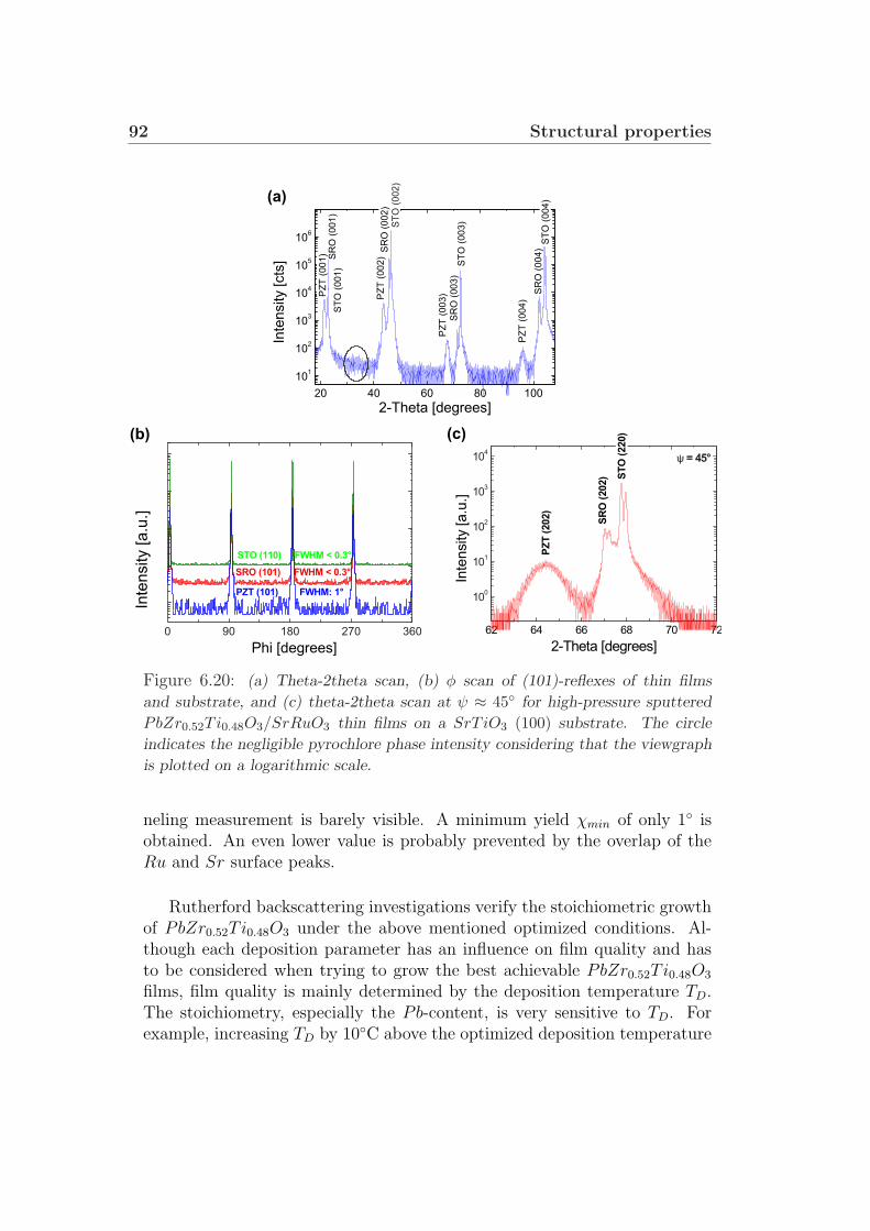
92 Structural properties
0 90 180 270 360
STO (110) FWHM < 0.3°
PZT (101) FWHM: 1°
SRO (101) FWHM < 0.3°
Phi [degrees]
Inte
nsity
[a.u
.]
(a)
(b)
20 40 60 80 100
101
102
103
104
105
106
ST
O (
004)
ST
O (
00
3)
SR
O (
002
)
SR
O (
003
)
SR
O (
004)
ST
O (
002)
ST
O (
001)
SR
O (
001
)
PZ
T (
003)
PZ
T (
00
4)P
ZT
(00
2)
PZ
T (
00
1)
Inte
nsity [cts
]
2-Theta [degrees]
62 64 66 68 70 72
100
101
102
103
104
ψ = 45°
ST
O (
220)
SR
O (
202)
PZ
T (
202)
Inte
nsity [a.u
.]
2-Theta [degrees]
(c)
Figure 6.20: (a) Theta-2theta scan, (b) φ scan of (101)-reflexes of thin films
and substrate, and (c) theta-2theta scan at ψ ≈ 45 for high-pressure sputtered
PbZr0.52Ti0.48O3/SrRuO3 thin films on a SrT iO3 (100) substrate. The circle
indicates the negligible pyrochlore phase intensity considering that the viewgraph
is plotted on a logarithmic scale.
neling measurement is barely visible. A minimum yield χmin of only 1 isobtained. An even lower value is probably prevented by the overlap of theRu and Sr surface peaks.
Rutherford backscattering investigations verify the stoichiometric growthof PbZr0.52Ti0.48O3 under the above mentioned optimized conditions. Al-though each deposition parameter has an influence on film quality and hasto be considered when trying to grow the best achievable PbZr0.52Ti0.48O3
films, film quality is mainly determined by the deposition temperature TD.The stoichiometry, especially the Pb-content, is very sensitive to TD. Forexample, increasing TD by 10C above the optimized deposition temperature
6.3 High-pressure sputtered SrRuO3 and Pb(Zr, T i)O3 thin films 93
(a) (b)
10 100
4.00
4.05
4.10
4.15
66
68
Cell V
olu
me [Å
3]
Out-of-plane
In-plane
Lattic
e P
ara
mete
r [Å
]
PbZr0.52
Ti0.48
O3 Film Thickness [nm]
0,00 0,05 0,10
-18
-16
-14
-12
-10
-8
-6
-4
-2
0
Mis
fit S
train
Sm [10
-3]
Inverse Film Thickness [nm-1]
Figure 6.21: (a) Thickness dependence of the out-of-plane and in-plane
lattice parameters of high-pressure sputtered PbZr0.52Ti0.48O3 thin films on
SrRuO3/SrT iO3 (100) substrates. The lines are only guides to the eyes and do
not correspond to a physical model. (b) Misfit-strain as a function of the inverse
film thickness.
leads to a 10% deficiency of the volatile lead. This results in a considerabledeterioration of the PbZr0.52Ti0.48O3 thin films as confirmed by XRD andRBS channeling investigations.
Fortunately, SrRuO3 does not only have an outstanding quality itself, butit also significantly improves the crystalline quality of PbZr0.52Ti0.48O3 thinfilms. Various PbZr0.52Ti0.48O3 thin films with thicknesses between 10 nmand 100 nm were grown on SrRuO3/SrT iO3 and on SrT iO3 substrates.The good quality of PbZr0.52Ti0.48O3 achieved on SrT iO3 substrates is sig-nificantly improved on SrRuO3/SrT iO3 substrates for all thicknesses. Asexample 60 nm thick PbZr0.52Ti0.48O3 films are shown in Fig. 6.22 (b) and(c) for their growth on different substrates. The interface peak is greatlyreduced for PbZr0.52Ti0.48O3 grown on SrRuO3/SrT iO3. This can be easilytaken from the Pb-signal in the channeling measurements (big arrow). Theimprovement of PbZr0.52Ti0.48O3 thin film quality is not only limited to theinterface region, but it is also true inside the film at a non-interface nearregion. In Ref. [193] we rule out the idea of a smaller lattice mismatch andfavorable thermal expansion coefficients as a possible explanation for theobserved improvement. A chemical interdiffusion across the interface dur-ing high-temperature film deposition, however, is possible. The formation ofSrPbO3 at the interface with a lattice parameter of 4.17 A might help to relaxthe in-plane strain and improve the interface between PbZr0.52Ti0.48O3 and

94 Structural properties
400 600 800 10000
500
1000
1500
2000
Inte
nsity [cts
]
Channel
0.4 0.5 0.7 0.8 1.0 1.1 1.2 1.4
OSr
Ti
Zr
Ru
Pb
χmin
= 8 %Random
Channeling
MeV
400 600 800 10000
500
1000
1500
2000
2500
Inte
nsity [cts
]
Channel
0,4 0,5 0,7 0,8 1,0 1,1 1,2 1,4
SrTi
Zr
Pb
χmin
= 16 %Random
Channeling
MeV
400 600 800 10000
500
1000
1500
O
Sr
Ru
Inte
nsity [cts
]
Channel
0.4 0.5 0.7 0.8 1.0 1.1 1.2 1.4
χmin
= 1 %
Random
Channeling
MeV(a)
(b) (c)
Figure 6.22: RBS random and channeling experiments for (a) 100 nm thick
SrRuO3 film on SrT iO3, (b) 60 nm thick PbZr0.52Ti0.48O3 film on SrT iO3 and
(c) 60 nm thick PbZr0.52Ti0.48O3 film on SrRuO3/SrT iO3.
SrRuO3/SrT iO3. This idea is supported by energy-dispersive x-ray spec-troscopy [194]. We believe, however, that the main reason for the improvedinterface as well as the enhanced crystalline quality of the PbZr0.52Ti0.48O3
thin films is the defined SrO termination at the SrRuO3 surface (see page 77).This may prevent the formation of grain boundaries, which can form at spotswhere different terminations are adjacent to each other [195].4
AFM measurements were performed to investigate the surface roughness.Flat surfaces with atomical steps were measured for 100 nm thick SrRuO3
on SrT iO3 samples (Fig. 6.23 (a)). The rms roughness of 1.6 A is even
4Note that the SrT iO3 (100) substrates were utilized as-delivered without any treat-ment prior to deposition. As a result, SrO and TiO2 terminations are present on thesesubstrates.
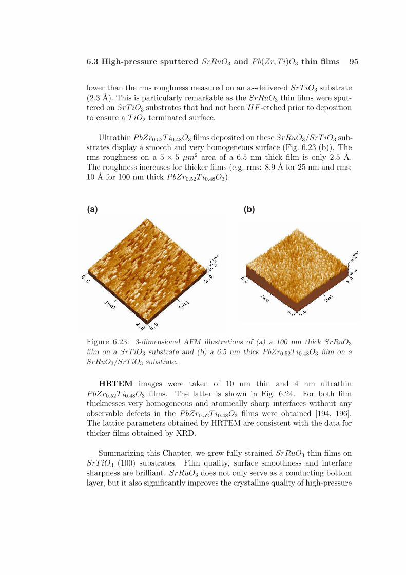
6.3 High-pressure sputtered SrRuO3 and Pb(Zr, T i)O3 thin films 95
lower than the rms roughness measured on an as-delivered SrT iO3 substrate(2.3 A). This is particularly remarkable as the SrRuO3 thin films were sput-tered on SrT iO3 substrates that had not been HF -etched prior to depositionto ensure a TiO2 terminated surface.
Ultrathin PbZr0.52Ti0.48O3 films deposited on these SrRuO3/SrT iO3 sub-strates display a smooth and very homogeneous surface (Fig. 6.23 (b)). Therms roughness on a 5 × 5 µm2 area of a 6.5 nm thick film is only 2.5 A.The roughness increases for thicker films (e.g. rms: 8.9 A for 25 nm and rms:10 A for 100 nm thick PbZr0.52Ti0.48O3).
(a) (b)
Figure 6.23: 3-dimensional AFM illustrations of (a) a 100 nm thick SrRuO3
film on a SrT iO3 substrate and (b) a 6.5 nm thick PbZr0.52Ti0.48O3 film on a
SrRuO3/SrT iO3 substrate.
HRTEM images were taken of 10 nm thin and 4 nm ultrathinPbZr0.52Ti0.48O3 films. The latter is shown in Fig. 6.24. For both filmthicknesses very homogeneous and atomically sharp interfaces without anyobservable defects in the PbZr0.52Ti0.48O3 films were obtained [194, 196].The lattice parameters obtained by HRTEM are consistent with the data forthicker films obtained by XRD.
Summarizing this Chapter, we grew fully strained SrRuO3 thin films onSrT iO3 (100) substrates. Film quality, surface smoothness and interfacesharpness are brilliant. SrRuO3 does not only serve as a conducting bottomlayer, but it also significantly improves the crystalline quality of high-pressure

96 Structural properties
4 nm PbZr0.52
Ti0.48
O3
SrRuO3
4 nm
SrRuO3
20 nm
SrTiO3
SrRuO3
SrRuO3
PZT
Figure 6.24: HRTEM image of a 4 nm thick PbZr0.52Ti0.48O3 film sandwiched
between SrRuO3 layers.
sputtered PbZr0.52Ti0.48O3 thin films. These films exhibit a high crystallinequality and ultrathin films are especially fascinating due to their smoothnessand interface sharpness.
Extrinsic effects on ferroelectricity, such as the influence of the capacitorpatterning method and the electrical boundary conditions will be demon-strated using high-pressure sputtered films in Chap. 7.1, p. 98 and p. 101.Ferroelectric properties and their thickness dependences for high-pressuresputtered PbZr0.52Ti0.48O3 based capacitors with the thicknessof the ferro-electric layer ranging from 8 nm to 250 nm will be discussed in Chap. 7.3.Finally, results for tunnel junctions with ultrathin PbZr0.52Ti0.48O3 barriers(3 nm - 6 nm) and studies of the current mechanism through these deviceswill be presented in Chapter 8.
Chapter 7
Ferroelectric properties
In order to measure ferroelectric properties, top electrode/FE layer/bottomelectrode heterostructures were patterned into capacitors with areas of 25×25 µm2 to 200 × 200 µm2. Three different methods, described below, wereused in this work to prepare capacitors.
The lift-off technique is shown schematically in Fig. 7.1 (a). Photoresist is spun on top of the ferroelectric thin film and conventional pho-tolithography defines the area of the capacitors. After sputtering Pt a lift-offprocess removes the photo resist together with the Pt in between the capac-itors.
The second method is an ion-beam etching (IBE) technique. First,all three layers of the heterostructure are deposited on the (100)-orientedSrT iO3 substrate. Conventional photolithography and an Ar-etching steptimed to stop in the ferroelectric layer or at the interface between bottomelectrode and ferroelectric layer define the shape and the area of the capaci-tors (Fig. 7.1 (b)).
The third method is a shadow mask technique, which is shown schemat-ically in Fig. 7.1 (c). Here, the top electrode is deposited through a shadowmask. The smallest areas obtained by this method and the specific shadowmask used here are about 1.5×103µm2. Size and shape of the capacitor areavary significantly from capacitor to capacitor. The areas of the capacitorshave to be determined by optical techniques and software solutions [197].The maximum error in the determination of area size is estimated to beabout ± 10%.
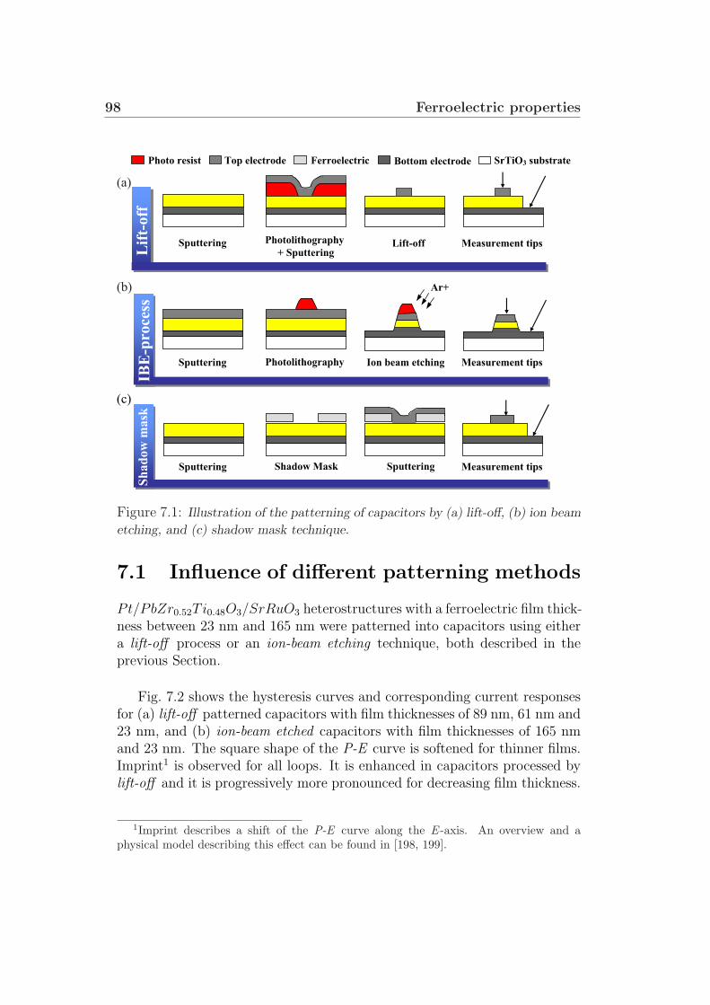
98 Ferroelectric properties
(a)
(b)
Photo resist Ferroelectric Bottom electrode SrTiO3 substrateTop electrode
Sputtering Photolithography
+ SputteringLift-off Measurement tips
Lif
t-off
IBE
-pro
cess
Ar+
Sputtering Photolithography Ion beam etching Measurement tips
Sh
ad
ow
ma
sk
(c)
Sputtering Measurement tipsSputteringShadow Mask
Figure 7.1: Illustration of the patterning of capacitors by (a) lift-off, (b) ion beam
etching, and (c) shadow mask technique.
7.1 Influence of different patterning methods
Pt/PbZr0.52Ti0.48O3/SrRuO3 heterostructures with a ferroelectric film thick-ness between 23 nm and 165 nm were patterned into capacitors using eithera lift-off process or an ion-beam etching technique, both described in theprevious Section.
Fig. 7.2 shows the hysteresis curves and corresponding current responsesfor (a) lift-off patterned capacitors with film thicknesses of 89 nm, 61 nm and23 nm, and (b) ion-beam etched capacitors with film thicknesses of 165 nmand 23 nm. The square shape of the P-E curve is softened for thinner films.Imprint1 is observed for all loops. It is enhanced in capacitors processed bylift-off and it is progressively more pronounced for decreasing film thickness.
1Imprint describes a shift of the P-E curve along the E -axis. An overview and aphysical model describing this effect can be found in [198, 199].
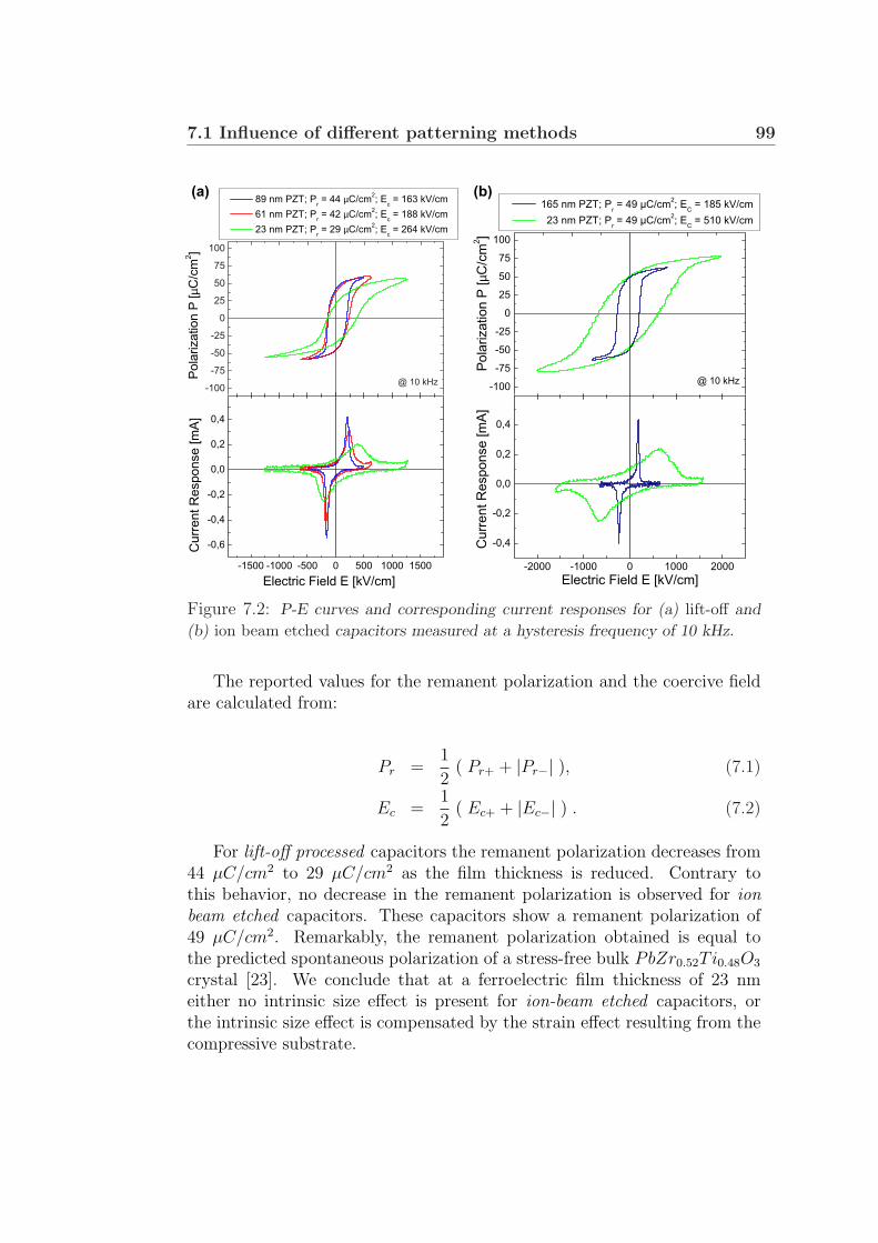
7.1 Influence of different patterning methods 99
-100
-75
-50
-25
0
25
50
75
100
@ 10 kHz
89 nm PZT; Pr = 44 µC/cm
2; E
c = 163 kV/cm
61 nm PZT; Pr = 42 µC/cm
2; E
c = 188 kV/cm
23 nm PZT; Pr = 29 µC/cm
2; E
c = 264 kV/cm
Pola
rization P
[µC
/cm
2]
-1500 -1000 -500 0 500 1000 1500
-0,6
-0,4
-0,2
0,0
0,2
0,4
Curr
ent R
esponse [m
A]
Electric Field E [kV/cm]
-2000 -1000 0 1000 2000
-0,4
-0,2
0,0
0,2
0,4
Curr
ent R
esponse [m
A]
Electric Field E [kV/cm]
-100
-75
-50
-25
0
25
50
75
100
@ 10 kHz
165 nm PZT; Pr = 49 µC/cm
2; E
C = 185 kV/cm
23 nm PZT; Pr = 49 µC/cm
2; E
C = 510 kV/cm
Pola
rization P
[µC
/cm
2]
(a) (b)
Figure 7.2: P-E curves and corresponding current responses for (a) lift-off and
(b) ion beam etched capacitors measured at a hysteresis frequency of 10 kHz.
The reported values for the remanent polarization and the coercive fieldare calculated from:
Pr =1
2( Pr+ + |Pr−| ), (7.1)
Ec =1
2( Ec+ + |Ec−| ) . (7.2)
For lift-off processed capacitors the remanent polarization decreases from44 µC/cm2 to 29 µC/cm2 as the film thickness is reduced. Contrary tothis behavior, no decrease in the remanent polarization is observed for ionbeam etched capacitors. These capacitors show a remanent polarization of49 µC/cm2. Remarkably, the remanent polarization obtained is equal tothe predicted spontaneous polarization of a stress-free bulk PbZr0.52Ti0.48O3
crystal [23]. We conclude that at a ferroelectric film thickness of 23 nmeither no intrinsic size effect is present for ion-beam etched capacitors, orthe intrinsic size effect is compensated by the strain effect resulting from thecompressive substrate.
100 Ferroelectric properties
The size effect observed for lift-off processed films cannot be explained byextrinsic effects, such as film composition or quality, as the thin film deposi-tion was identical for both patterning techniques. A possible explanation forthe reduced remanent polarization could be a chemical decomposition of theferroelectric layer at the surface, due to its exposure to solvents, photo resist,and developer during the lift-off process. This possibly leads to (sub-)surfacelayers in the ferroelectric film with suppressed ferroelectric properties.
The measured current responses shown in Fig. 7.2 (a) and (b) for lift-off and ion-beam etched capacitors, respectively, strongly indicate that thelift-off process damages the surface of the ferroelectric layer. Leakage cur-rents increase for lift-off processed capacitors first for positive voltages atthe top electrode (corresponding to positive electric fields in the current re-sponse). In contrast, for ion beam etched capacitors the leakage currentsfor positive voltages at the top electrode are considerably lower. Therefore,higher electric fields can be applied if necessary to saturate the P-E curveof capacitors with thinner PbZr0.52Ti0.48O3 films. Here, leakage currentsappear first for positive voltages at the bottom electrode (corresponding tonegative electric fields in the current response). This observation suggeststhat leakage currents in ion-beam etched capacitors first originate from thePbZr0.52Ti0.48O3/SrRuO3 interface, whereas leakage currents for lift-off pro-cessed capacitors already increase with smaller applied electric fields origi-nating from the Pt/PbZr0.52Ti0.48O3 interface. As a consequence of leakagecurrents, it might not be possible to apply sufficiently large bias-voltages2 inorder to saturate the P-E curves.
We believe that the PbZr0.52Ti0.48O3 surface treatment during the lift-offprocess results in a damaged surface layer leading to a reduced remanentpolarization for thicker films. In addition, the typically observed increase ofthe coercive field for thinner films [200], and the non-saturation of the P-Ecurves due to increased leakage currents at higher voltages are responsiblefor the decreased remanent polarization for thinner films.
The second striking feature, which can be observed in Fig. 7.2 (a) and(b), is the increasing coercive field as the film thickness is decreased. Thisbehavior is obtained irrespective of the patterning technique. However, thereported increase is considerably stronger in ion-beam etched capacitors.
2The application of a sufficiently large bias-voltage leads to the integration of highleakage currents (in addition to the displacement current). In this case, the P-E curvewould not be the result of the integration of the displacement current.
7.2 Influence of boundary conditions 101
We believe that a larger surface roughness arises from the surface treat-ment during the lift-off patterning, leading to the weaker increase of the coer-cive field obtained for lift-off processed capacitors in comparison to ion-beametched capacitors. Surface roughness at the interface leads to an inhomoge-neous field distribution at the Pt/PbZr0.52Ti0.48O3 interface. In other words,the electric field at the interface is locally enhanced. As a result, the polar-ization reversal is likely to start at lower externally applied electric fields (cf.Fig. 1.6).
We conclude that etch degradation and residuals at the edges of the ca-pacitors are less significant than the contact of the PbZr0.52Ti0.48O3 surfacewith chemical solvents during lift-off processing. Nevertheless, in order toavoid any possible risk resulting from the contact of the ferroelectric surfacewith chemical solvents and from etch degradation and residuals, a shadowmask was used to fabricate the capacitors characterized in Chap. 7.3. Re-cently, our research group started using nano-stencil masks [201]. Thesespecific shadow masks allow the fabrication of capacitors with sub-µm areaswithout damaging the ferroelectric layer.
7.2 Influence of boundary conditions
In Chap. 1.3 and 1.4, the influence of boundary conditions on ferroelec-tricity has been extensively discussed from a theoretical point of view. Inthis Chapter it will be shown how boundary conditions may affect the specificexperimental results.
Influence of electrical boundary conditions
The influence of the top electrode material on the ferroelectric properties offerroelectric capacitors was studied. For this purpose SrRuO3/PbZr0.52Ti0.48O3/SrRuO3 and Pt/PbZr0.52Ti0.48O3/SrRuO3 hetero-structures were grown on SrT iO3 (100) substrates. These heterostructuresshown in the TEM images (Fig. 7.3) were processed into capacitors using ionbeam etching (Fig. 7.1 (b)).
In Fig. 7.4 (a) the P-E loop for a 23 nm thick PbZr0.52Ti0.48O3 filmsandwiched between the SrRuO3 top and bottom electrodes is shown. Forcomparison the P-E loop and current response for a similar capacitor with
102 Ferroelectric properties
100 nm
Pt
Pb(Zr,Ti)O3
SrRuO3
SrTiO3100 nm
SrRuO3
Pb(Zr,Ti)O3
SrRuO3
SrTiO3
(a) (b)
Figure 7.3: TEM images of (a) SrRuO3/PbZr0.52Ti0.48O3/SrRuO3, and (b)
Pt/PbZr0.52Ti0.48O3/SrRuO3 heterostructures.
Pt top electrode is displayed in Fig. 7.4 (b). Both capacitors, the one withSrRuO3 top electrode and the one with Pt top electrode, were measuredat a hysteresis frequency of 10 kHz. These P-E curves are typical of allinvestigated film thicknesses (12 nm - 60 nm) and all measured frequencies(1 kHz - 250 kHz).
The remanent polarization of capacitors with SrRuO3 top electrodes doesnot reach the value of 49 µC/cm2. The coercive field for these heterostruc-
-1500 -1000 -500 0 500 1000 1500
-100
-75
-50
-25
0
25
50
75
100
@ 10 kHz
Curre
nt R
esponse [m
A]
Voltage [V]
SrRuO3 top electrode
Pr = 34 µC/cm
2
Ec = 362 kV/cm
Pola
rization P
[µC
/cm
2]
Electric Field E [kV/cm]
-4 -2 0 2 4
-0,2
0,0
0,2
(a) (b)
-1500 -1000 -500 0 500 1000 1500
-100
-75
-50
-25
0
25
50
75
100
-4 -2 0 2 4
-0,6
-0,3
0,0
0,3
0,6
Curre
nt R
esponse [m
A]
Voltage [V]
Pola
rization P
[µC
/cm
2]
Electric Field E [kV/cm]
Pt top electrode
Pr = 49 µC/cm
2
Ec = 472 kV/cm
@ 10 kHz
Figure 7.4: P-E curves and corresponding voltage dependences of
the current response for (a) SrRuO3/PbZr0.52Ti0.48O3/SrRuO3, and
(b) Pt/PbZr0.52Ti0.48O3/SrRuO3 capacitors with a ferroelectric layer thickness
of 23 nm.

7.2 Influence of boundary conditions 103
tures is lower compared to capacitors having Pt top electrodes. These state-ments are especially true of thinner ferroelectric films.
The most striking feature, however, is the voltage dependence of the cur-rent response for PbZr0.52Ti0.48O3 films with SrRuO3 top electrode. Highleakage currents for positive voltages at the top electrode are present (largearrow). No clear switching current is observed. Indeed, two maxima in thedisplacement current part of the current response are visible for each direc-tion indicated by tiny arrows. It is difficult to speculate about the reasonsfor these two maxima. Maybe some regions inside the ferroelectric film arepinned at defects introduced during the sputtering of the top electrode. An-other possible explanation is that 90 and 180 domains are present and havedifferent coercive fields. Irrespective of the reason for the observed doublepeaks, what is obvious from Fig. 7.4 (a) is the fact that the P-E curve is notsaturated. In other words, the polarization reversal is not complete.
The use of SrRuO3 top electrodes, and generally the use of oxide elec-trodes, has been shown to reduce fatigue3 [151] in ferroelectric capacitors. Onthe other hand, we demonstrated that the use of SrRuO3 top electrodes en-hances leakage currents [199]. This can be attributed to a lower barrier heightfor SrRuO3/Pb(Zr, T i)O3 compared to Pt/Pb(Zr, T i)O3 (see Chap. 4.1).Due to the increased leakage currents, and the increasing coercive field fordecreasing film thickness, saturation of the P-E loop is challenging. As aresult, the remanent polarization decreases for thinner films. This size effect,however, is not intrinsic to the ferroelectric film. The nature of this effect isclearly extrinsic. It is associated with the choice of the electrical boundaryconditions.
We conclude that in addition to the thin film quality and the fabricationprocess of the capacitors, the choice of the electrode material is crucial aswell. Hence, the influence of electrical boundary conditions on ferroelectricityhas been successfully verified.
Influence of mechanical boundary conditions
In this Section I will try to experimentally verify two predictions discussedin Chap. 1.4 concerning the influence of compressive substrates. First, itwill be investigated whether the elongated out-of-plane lattice parameter for
3Fatigue is one of the failure mechanisms of non-volatile ferroelectric memory devices;it describes the loss in the remanent polarization as a function of cycles. Various possibleorigins of fatigue are discussed in Refs. [202, 203, 204, 205, 206, 207, 208].
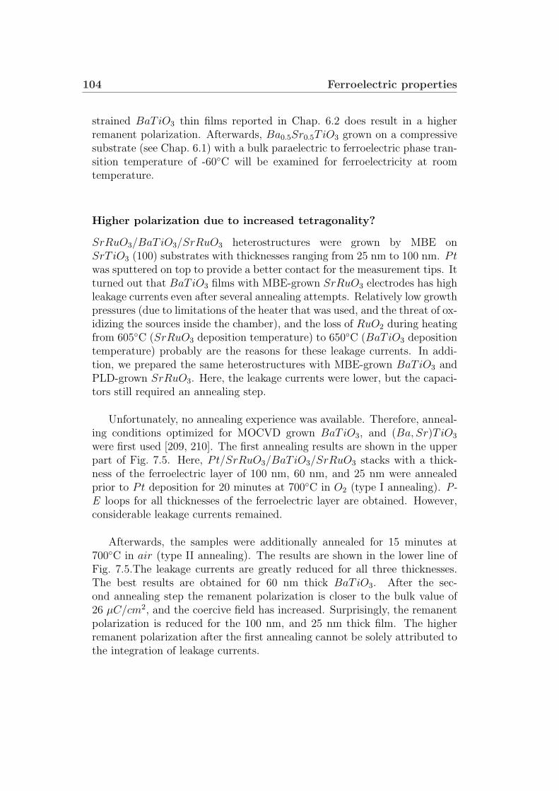
104 Ferroelectric properties
strained BaTiO3 thin films reported in Chap. 6.2 does result in a higherremanent polarization. Afterwards, Ba0.5Sr0.5TiO3 grown on a compressivesubstrate (see Chap. 6.1) with a bulk paraelectric to ferroelectric phase tran-sition temperature of -60C will be examined for ferroelectricity at roomtemperature.
Higher polarization due to increased tetragonality?
SrRuO3/BaT iO3/SrRuO3 heterostructures were grown by MBE onSrT iO3 (100) substrates with thicknesses ranging from 25 nm to 100 nm. Ptwas sputtered on top to provide a better contact for the measurement tips. Itturned out that BaTiO3 films with MBE-grown SrRuO3 electrodes has highleakage currents even after several annealing attempts. Relatively low growthpressures (due to limitations of the heater that was used, and the threat of ox-idizing the sources inside the chamber), and the loss of RuO2 during heatingfrom 605C (SrRuO3 deposition temperature) to 650C (BaTiO3 depositiontemperature) probably are the reasons for these leakage currents. In addi-tion, we prepared the same heterostructures with MBE-grown BaTiO3 andPLD-grown SrRuO3. Here, the leakage currents were lower, but the capaci-tors still required an annealing step.
Unfortunately, no annealing experience was available. Therefore, anneal-ing conditions optimized for MOCVD grown BaTiO3, and (Ba, Sr)TiO3
were first used [209, 210]. The first annealing results are shown in the upperpart of Fig. 7.5. Here, Pt/SrRuO3/BaT iO3/SrRuO3 stacks with a thick-ness of the ferroelectric layer of 100 nm, 60 nm, and 25 nm were annealedprior to Pt deposition for 20 minutes at 700C in O2 (type I annealing). P-E loops for all thicknesses of the ferroelectric layer are obtained. However,considerable leakage currents remained.
Afterwards, the samples were additionally annealed for 15 minutes at700C in air (type II annealing). The results are shown in the lower line ofFig. 7.5.The leakage currents are greatly reduced for all three thicknesses.The best results are obtained for 60 nm thick BaTiO3. After the sec-ond annealing step the remanent polarization is closer to the bulk value of26 µC/cm2, and the coercive field has increased. Surprisingly, the remanentpolarization is reduced for the 100 nm, and 25 nm thick film. The higherremanent polarization after the first annealing cannot be solely attributed tothe integration of leakage currents.
7.2 Influence of boundary conditions 105
-200 -100 0 100 200
-20
-10
0
10
20
@ 150 kHz
Voltage [V]
Pr = 17 µC/cm
2
Ec = 68 kV/cm
Pola
rization P
[µC
/cm
2]
Electric Field E [kV/cm]
-2 -1 0 1 2
-400 -200 0 200 400
-20
-10
0
10
20
@ 250 kHz
Voltage [V]
Pr = 13 µC/cm
2
Ec = 68 kV/cm
Pola
rization P
[µC
/cm
2]
Electric Field E [kV/cm]
-2 -1 0 1 2
-900 -600 -300 0 300 600 900
-20
-15
-10
-5
0
5
10
15
20
@ 100 kHz
Voltage [V]
Pr = 8 µC/cm
2
Ec = 176 kV/cm
Pola
rization P
[µC
/cm
2]
Electric Field E [kV/cm]
-2 -1 0 1 2
100 nm BaTiO3 60 nm BaTiO3 25 nm BaTiO3
-300 -200 -100 0 100 200 300-20
-10
0
10
20
Voltage [V]
Pr = 10 µC/cm
2
Ec = 57 kV/cm
Pola
rization P
[µC
/cm
2]
Electric Field E [kV/cm]
-3 -2 -1 0 1 2 3
@ 140 kHz
-400 -200 0 200 400-30
-20
-10
0
10
20
30
@ 250 kHz
Voltage [V]
Pr = 17 µC/cm
2
Ec = 80 kV/cm
Po
larizatio
n P
[µC
/cm
2]
Electric Field E [kV/cm]
-2 -1 0 1 2
-1000 -500 0 500 1000-4
-2
0
2
4
Voltage [V]
Pr = 2 µC/cm
2
Ec = 326 kV/cm
Po
larizatio
n P
[µC
/cm
2]
Electric Field E [kV/cm]
-2 -1 0 1 2 3
@100 kHz
Type I
annealing
Type I +
Type II
annealing
(a) (b) (c)
Figure 7.5: P-E curves for Pt/SrRuO3/BaT iO3/SrRuO3 capacitors with a fer-
roelectric layer thickness of (a) 100 nm (b) 60 nm, and (c) 25 nm. The upper part
shows P-E curves for capacitors that were annealed at 700C in O2 prior to Pt
deposition and patterning (type I annealing). For the measurements in the lower
part, the capacitors were additionally annealed at 700C in air after the deposition
of the complete stack and after ion-beam etching patterning (type II annealing).
Our conclusion from these and other annealing experiments carried outat different temperatures for some few minutes up to several hours, in air,in N2, and in O2 is that of the conditions investigated, annealing in air for20 minutes at 700C is best for 60 nm thick films. Under these optimized an-nealing conditions the P-E loops are nicely shaped, have low leakage currentsat a frequency of 30 kHz, and show high values for the remanent polarization(Fig. 7.6 (a)). As expected for oxide electrodes, no fatigue is observed up toat least 1011 cycles (Fig. 7.6 (b)).
In summary, the main challenge for MBE-grown BaTiO3 thin films isthe determination of an adequate annealing process. A large decrease in theleakage current can be achieved leading to nicely shaped and fatigue-free P-E curves with high values for the remanent polarization. However, differentthicknesses of the ferroelectric layer require different annealing conditions.As a result, it is hardly possible to evaluate size effects in these samples.A higher remanent polarization due to the larger tetragonality for strainedBaTiO3 with thicknesses up to 25 nm could not be verified. A comprehen-
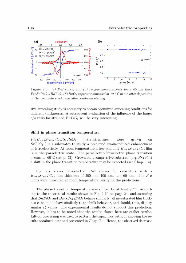
106 Ferroelectric properties
-300 -200 -100 0 100 200 300
-40
-20
0
20
40
Curre
nt R
esponse [m
A]
Voltage [V]
65 nm BaTiO3
Pr = 21 µC/cm
2
Ec = 35 kV/cm
Pola
rization P
[µC
/cm
2]
Electric Field E [kV/cm]
-2,0 -1,0 0,0 1,0 2,0
-0,02
-0,01
0,00
0,01
0,02
@ 30 kHz
0 2 4 6 8 10 12
-1,0
-0,5
0,0
0,5
1,0
@ 50 kHz
Pr /
Pr0
cycles [log n]
(a) (b)
Figure 7.6: (a) P-E curve, and (b) fatigue measurements for a 65 nm thick
Pt/SrRuO3/BaT iO3/SrRuO3 capacitor annealed at 700C in air after deposition
of the complete stack, and after ion-beam etching.
sive annealing study is necessary to obtain optimized annealing conditions fordifferent thicknesses. A subsequent evaluation of the influence of the largerc/a ratio for strained BaTiO3 will be very interesting.
Shift in phase transition temperature
Pt/Ba0.5Sr0.5TiO3/SrRuO3 heterostructures were grown onSrT iO3 (100) substrates to study a predicted strain-induced enhancementof ferroelectricity. At room temperature a free-standing Ba0.5Sr0.5TiO3 filmis in the paraelectric state. The paraelectric-ferroelectric phase transitionoccurs at -60C (see p. 53). Grown on a compressive substrate (e.g. SrT iO3)a shift in the phase transition temperature may be expected (see Chap. 1.4).
Fig. 7.7 shows ferroelectric P-E curves for capacitors with aBa0.5Sr0.5TiO3 film thickness of 200 nm, 100 nm, and 60 nm. The P-Eloops were measured at room temperature, verifying the predictions.
The phase transition temperature was shifted by at least 85C. Accord-ing to the theoretical results shown in Fig. 1.10 on page 24, and assumingthat BaTiO3 and Ba0.5Sr0.5TiO3 behave similarly, all investigated film thick-nesses should behave similarly to the bulk behavior, and should, thus, displaysimilar Pr values. The experimental results do not support this prediction.However, it has to be noted that the results shown here are earlier results.Lift-off processing was used to pattern the capacitors without knowing the re-sults obtained later and presented in Chap. 7.1. Hence, the observed decrease
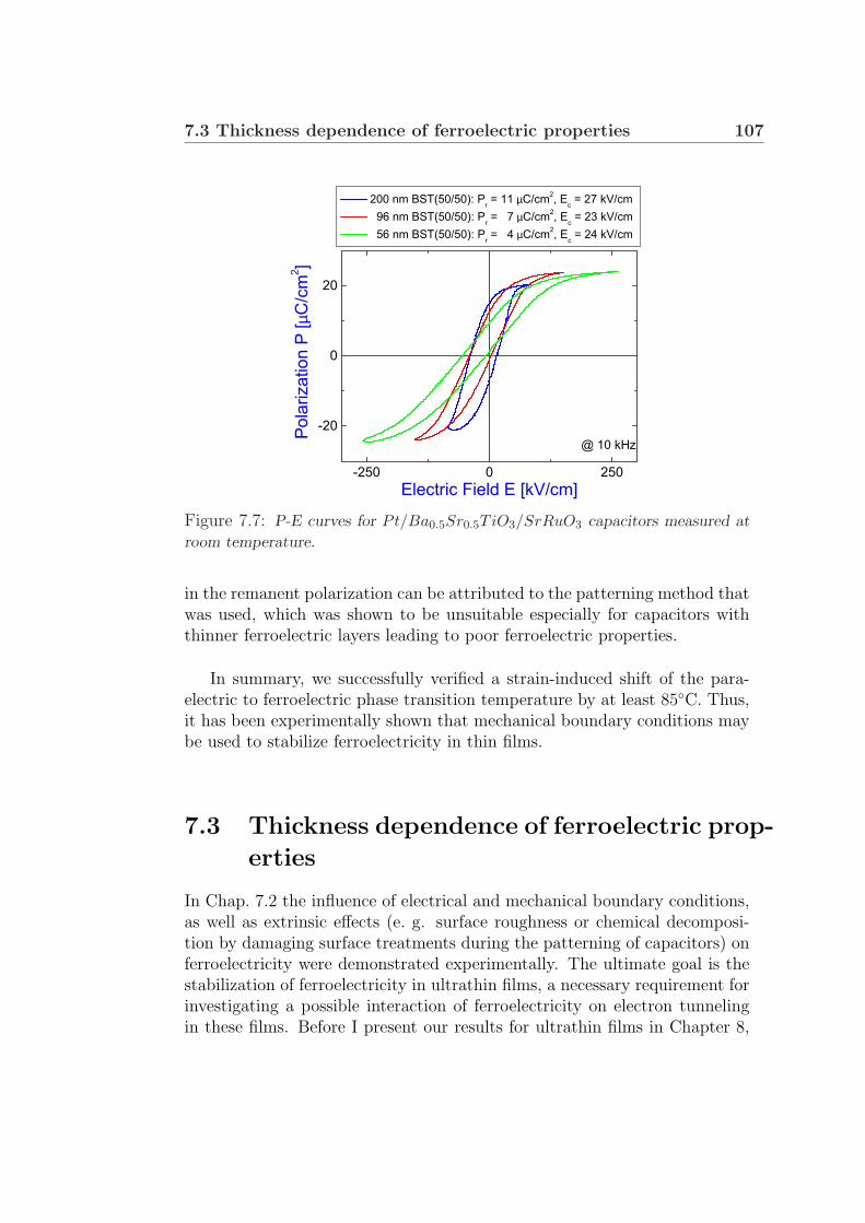
7.3 Thickness dependence of ferroelectric properties 107
-250 0 250
-20
0
20
@ 10 kHz
200 nm BST(50/50): Pr = 11 µC/cm
2, E
c = 27 kV/cm
96 nm BST(50/50): Pr = 7 µC/cm
2, E
c = 23 kV/cm
56 nm BST(50/50): Pr = 4 µC/cm
2, E
c = 24 kV/cm
Pola
rization P
[µC
/cm
2]
Electric Field E [kV/cm]
Figure 7.7: P-E curves for Pt/Ba0.5Sr0.5TiO3/SrRuO3 capacitors measured at
room temperature.
in the remanent polarization can be attributed to the patterning method thatwas used, which was shown to be unsuitable especially for capacitors withthinner ferroelectric layers leading to poor ferroelectric properties.
In summary, we successfully verified a strain-induced shift of the para-electric to ferroelectric phase transition temperature by at least 85C. Thus,it has been experimentally shown that mechanical boundary conditions maybe used to stabilize ferroelectricity in thin films.
7.3 Thickness dependence of ferroelectric prop-
erties
In Chap. 7.2 the influence of electrical and mechanical boundary conditions,as well as extrinsic effects (e. g. surface roughness or chemical decomposi-tion by damaging surface treatments during the patterning of capacitors) onferroelectricity were demonstrated experimentally. The ultimate goal is thestabilization of ferroelectricity in ultrathin films, a necessary requirement forinvestigating a possible interaction of ferroelectricity on electron tunnelingin these films. Before I present our results for ultrathin films in Chapter 8,
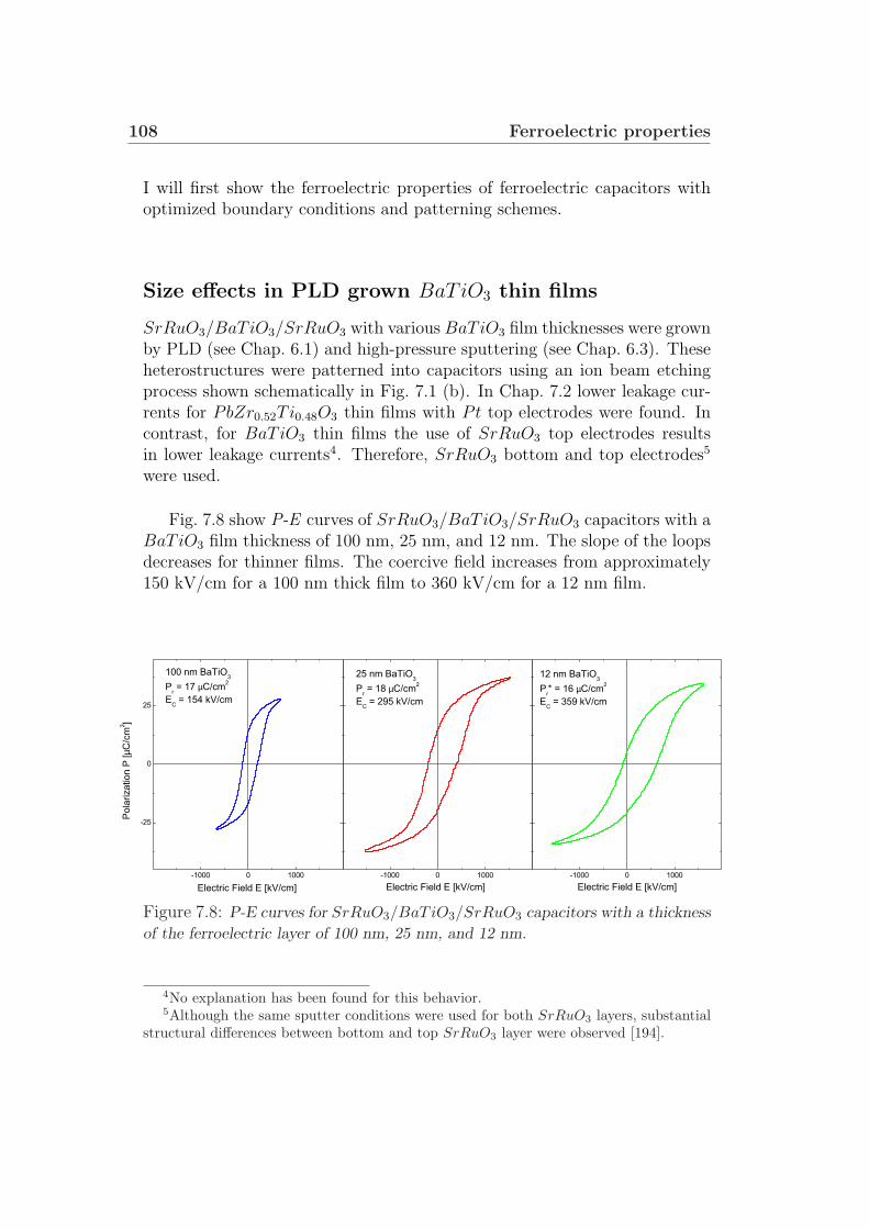
108 Ferroelectric properties
I will first show the ferroelectric properties of ferroelectric capacitors withoptimized boundary conditions and patterning schemes.
Size effects in PLD grown BaTiO3 thin films
SrRuO3/BaT iO3/SrRuO3 with various BaTiO3 film thicknesses were grownby PLD (see Chap. 6.1) and high-pressure sputtering (see Chap. 6.3). Theseheterostructures were patterned into capacitors using an ion beam etchingprocess shown schematically in Fig. 7.1 (b). In Chap. 7.2 lower leakage cur-rents for PbZr0.52Ti0.48O3 thin films with Pt top electrodes were found. Incontrast, for BaTiO3 thin films the use of SrRuO3 top electrodes resultsin lower leakage currents4. Therefore, SrRuO3 bottom and top electrodes5
were used.
Fig. 7.8 show P-E curves of SrRuO3/BaT iO3/SrRuO3 capacitors with aBaTiO3 film thickness of 100 nm, 25 nm, and 12 nm. The slope of the loopsdecreases for thinner films. The coercive field increases from approximately150 kV/cm for a 100 nm thick film to 360 kV/cm for a 12 nm film.
-1000 0 1000-1000 0 1000-1000 0 1000
-25
0
25
12 nm BaTiO3
Pr* = 16 µC/cm
2
EC = 359 kV/cm
Electric Field E [kV/cm]Electric Field E [kV/cm] Electric Field E [kV/cm]
25 nm BaTiO3
Pr = 18 µC/cm
2
EC = 295 kV/cm
Pola
rization P
[µC
/cm
2]
100 nm BaTiO3
Pr = 17 µC/cm
2
EC = 154 kV/cm
Figure 7.8: P-E curves for SrRuO3/BaT iO3/SrRuO3 capacitors with a thickness
of the ferroelectric layer of 100 nm, 25 nm, and 12 nm.
4No explanation has been found for this behavior.5Although the same sputter conditions were used for both SrRuO3 layers, substantial
structural differences between bottom and top SrRuO3 layer were observed [194].
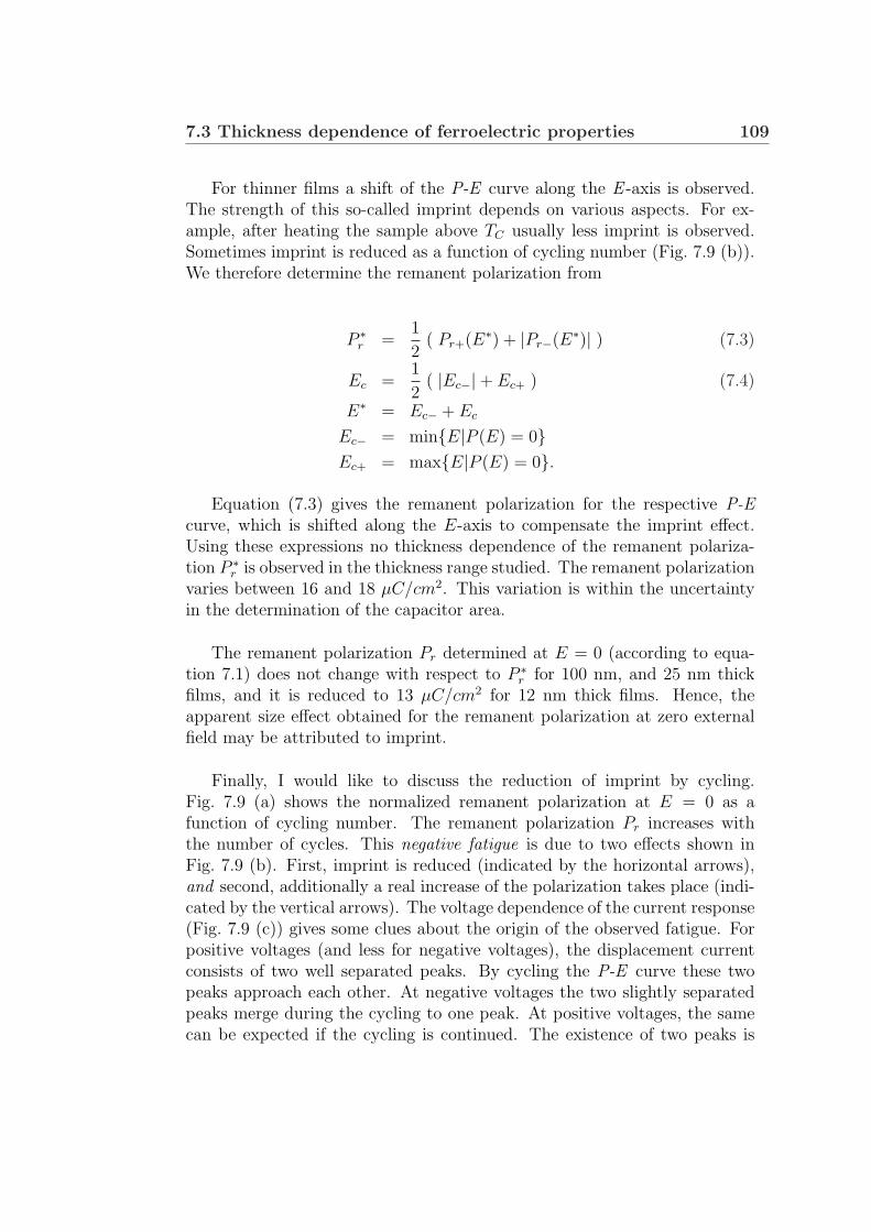
7.3 Thickness dependence of ferroelectric properties 109
For thinner films a shift of the P-E curve along the E -axis is observed.The strength of this so-called imprint depends on various aspects. For ex-ample, after heating the sample above TC usually less imprint is observed.Sometimes imprint is reduced as a function of cycling number (Fig. 7.9 (b)).We therefore determine the remanent polarization from
P ∗r =
1
2( Pr+(E∗) + |Pr−(E∗)| ) (7.3)
Ec =1
2( |Ec−|+ Ec+ ) (7.4)
E∗ = Ec− + Ec
Ec− = minE|P (E) = 0Ec+ = maxE|P (E) = 0.
Equation (7.3) gives the remanent polarization for the respective P-Ecurve, which is shifted along the E-axis to compensate the imprint effect.Using these expressions no thickness dependence of the remanent polariza-tion P ∗
r is observed in the thickness range studied. The remanent polarizationvaries between 16 and 18 µC/cm2. This variation is within the uncertaintyin the determination of the capacitor area.
The remanent polarization Pr determined at E = 0 (according to equa-tion 7.1) does not change with respect to P ∗
r for 100 nm, and 25 nm thickfilms, and it is reduced to 13 µC/cm2 for 12 nm thick films. Hence, theapparent size effect obtained for the remanent polarization at zero externalfield may be attributed to imprint.
Finally, I would like to discuss the reduction of imprint by cycling.Fig. 7.9 (a) shows the normalized remanent polarization at E = 0 as afunction of cycling number. The remanent polarization Pr increases withthe number of cycles. This negative fatigue is due to two effects shown inFig. 7.9 (b). First, imprint is reduced (indicated by the horizontal arrows),and second, additionally a real increase of the polarization takes place (indi-cated by the vertical arrows). The voltage dependence of the current response(Fig. 7.9 (c)) gives some clues about the origin of the observed fatigue. Forpositive voltages (and less for negative voltages), the displacement currentconsists of two well separated peaks. By cycling the P-E curve these twopeaks approach each other. At negative voltages the two slightly separatedpeaks merge during the cycling to one peak. At positive voltages, the samecan be expected if the cycling is continued. The existence of two peaks is
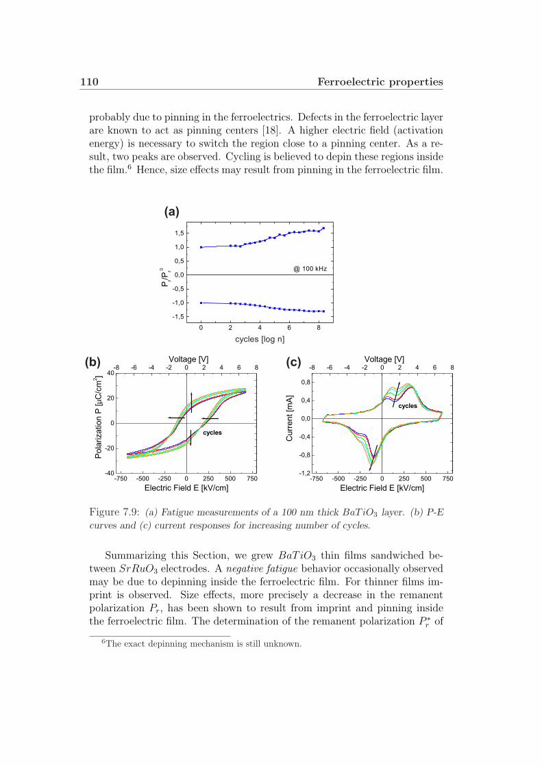
110 Ferroelectric properties
probably due to pinning in the ferroelectrics. Defects in the ferroelectric layerare known to act as pinning centers [18]. A higher electric field (activationenergy) is necessary to switch the region close to a pinning center. As a re-sult, two peaks are observed. Cycling is believed to depin these regions insidethe film.6 Hence, size effects may result from pinning in the ferroelectric film.
-750 -500 -250 0 250 500 750-40
-20
0
20
40
cycles
Voltage [V]
Pola
rization P
[µC
/cm
2]
Electric Field E [kV/cm]
-8 -6 -4 -2 0 2 4 6 8
-750 -500 -250 0 250 500 750-1,2
-0,8
-0,4
0,0
0,4
0,8
cycles
Curr
ent [m
A]
Voltage [V]
Electric Field E [kV/cm]
-8 -6 -4 -2 0 2 4 6 8
0 2 4 6 8
-1,5
-1,0
-0,5
0,0
0,5
1,0
1,5
@ 100 kHz
Pr/P
r0
cycles [log n]
(a)
(b) (c)
Figure 7.9: (a) Fatigue measurements of a 100 nm thick BaTiO3 layer. (b) P-E
curves and (c) current responses for increasing number of cycles.
Summarizing this Section, we grew BaTiO3 thin films sandwiched be-tween SrRuO3 electrodes. A negative fatigue behavior occasionally observedmay be due to depinning inside the ferroelectric film. For thinner films im-print is observed. Size effects, more precisely a decrease in the remanentpolarization Pr, has been shown to result from imprint and pinning insidethe ferroelectric film. The determination of the remanent polarization P ∗
r of
6The exact depinning mechanism is still unknown.
7.3 Thickness dependence of ferroelectric properties 111
I-V curves, which are shifted along the E-axis to compensate the imprint ef-fect, should be performed according to eqn. (7.3,7.4). Using these equationsand cycling the samples (if necessary), no decrease in the remanent polariza-tion P ∗
r is obtained for BaTiO3 thin films ranging from 12 nm to 100 nm.However, an increase of the coercive field for thinner films is observed. Thisincrease does not depend on imprint or pinning of the ferroelectric film.
Size effects in high-pressure sputtered PbZr0.52Ti0.48O3
thin films
PbZr0.52Ti0.48O3 with film thicknesses ranging from 6 nm to 250 nm weregrown by high-pressure sputtering on SrRuO3/SrT iO3 substrates. After-wards, Pt was evaporated through a shadow mask.
Fig. 7.10 (a) and (b) show the P-E curves and the corresponding currentresponses for 135 nm, and 10 nm thick PbZr0.52Ti0.48O3 films. P-E curves ofthick films (t > 30 nm) are nicely shaped and possess outstanding squareness.For decreasing film thickness the coercive field increases and the displacementcurrent peaks arising from the polarization reversals are broadened.
Imprint, present also in thicker films, is especially observable in thinnerfilms. As the film thickness decreases the curves are progressively shiftedalong the E -axis. The current response (and P-E curve) for the only 10 nmthick ferroelectric film best demonstrates the effect of imprint. After switch-ing from the negative to the positive polarization state by applying a positivevoltage, back-switching to negative polarization values takes place at zerovolt. Imprint is the result of an internal field. This internal field is largeenough to (partially) reverse the polarization in the absence of any appliedexternal field. The origin of this internal field is currently being discussed inthe literature [198, 199].
Leakage currents rise for thinner films. They are considered to be inde-pendent of the hysteresis frequency [211]. At the same time, the displacementcurrent (current that arises from the displacement of the ions during the po-larization reversal) does depend on the hysteresis frequency. The higher thehysteresis frequency the faster the ions are displaced, and the larger the dis-placement current (I = Q) is which results from this displacement. Fornot too high leakage currents, the application of high frequencies results ina current response dominated by the displacement current. Unfortunately,
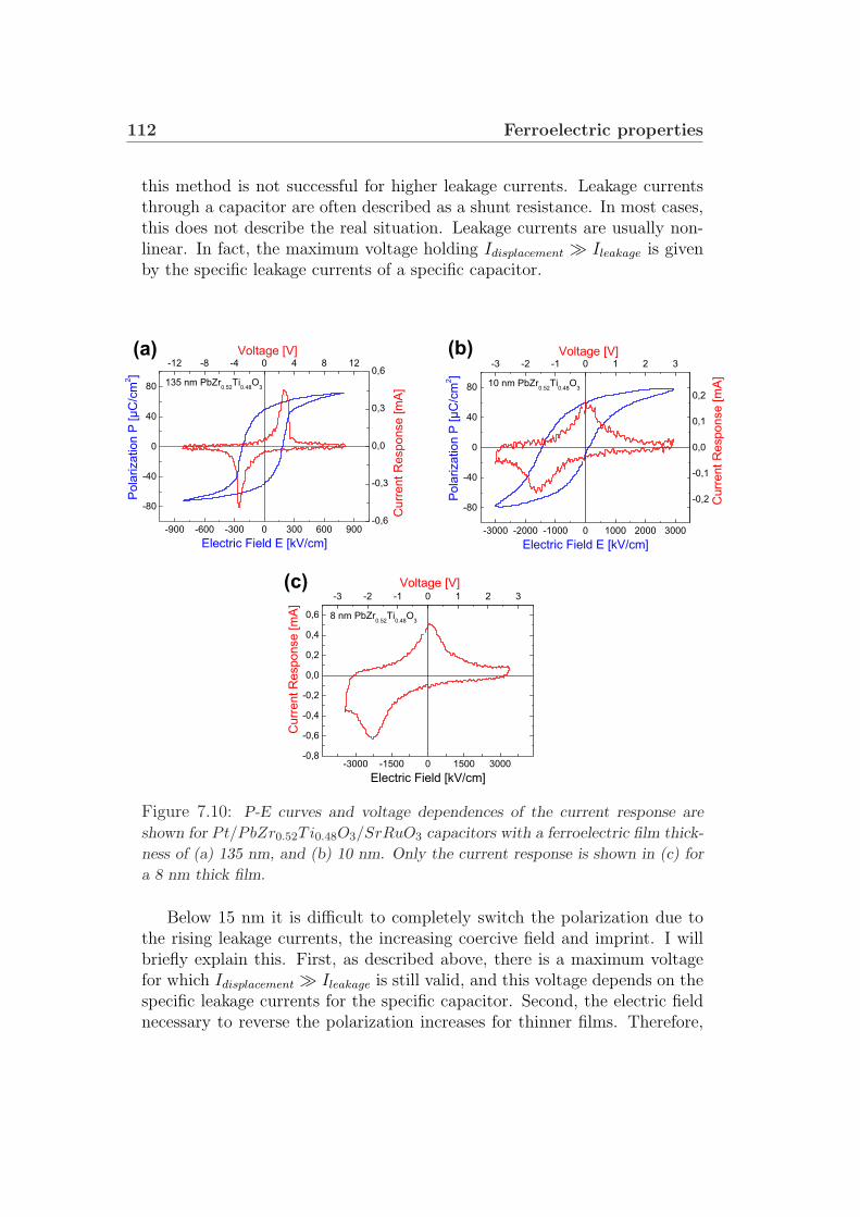
112 Ferroelectric properties
this method is not successful for higher leakage currents. Leakage currentsthrough a capacitor are often described as a shunt resistance. In most cases,this does not describe the real situation. Leakage currents are usually non-linear. In fact, the maximum voltage holding Idisplacement À Ileakage is givenby the specific leakage currents of a specific capacitor.
-900 -600 -300 0 300 600 900
-80
-40
0
40
80
Voltage [V]
135 nm PbZr0.52
Ti0.48
O3
Pola
rization P
[µ
C/c
m2]
Electric Field E [kV/cm]
-12 -8 -4 0 4 8 12
-0,6
-0,3
0,0
0,3
0,6
Curr
ent R
esponse [m
A]
-3000 -2000 -1000 0 1000 2000 3000
-80
-40
0
40
80
Voltage [V]
Curr
ent R
esponse [m
A]
10 nm PbZr0.52
Ti0.48
O3
Pola
rization P
[µ
C/c
m2]
Electric Field E [kV/cm]
-3 -2 -1 0 1 2 3
-0,2
-0,1
0,0
0,1
0,2
(a) (b)
(c)
-3000 -1500 0 1500 3000-0,8
-0,6
-0,4
-0,2
0,0
0,2
0,4
0,6
-3 -2 -1 0 1 2 3
Voltage [V]
8 nm PbZr0.52
Ti0.48
O3
Curr
ent R
esponse [m
A]
Electric Field [kV/cm]
Figure 7.10: P-E curves and voltage dependences of the current response are
shown for Pt/PbZr0.52Ti0.48O3/SrRuO3 capacitors with a ferroelectric film thick-
ness of (a) 135 nm, and (b) 10 nm. Only the current response is shown in (c) for
a 8 nm thick film.
Below 15 nm it is difficult to completely switch the polarization due tothe rising leakage currents, the increasing coercive field and imprint. I willbriefly explain this. First, as described above, there is a maximum voltagefor which Idisplacement À Ileakage is still valid, and this voltage depends on thespecific leakage currents for the specific capacitor. Second, the electric fieldnecessary to reverse the polarization increases for thinner films. Therefore,
7.3 Thickness dependence of ferroelectric properties 113
the corresponding voltage does not decrease as rapidly as expected. Finally,imprint causes a complete switching of the polarization in one direction atvery low external applied voltages, but at the same time it takes a consid-erably higher voltage (coercive voltage + voltage to neutralize the internalfield) to switch to the opposite polarization state.
Nevertheless, even an 8 nm thick PbZr0.52Ti0.48O3 film is clearly ferro-electric. Figure 7.10 (c) shows the polarization reversals demonstrating ferro-electricity. Due to high leakage currents at negative voltages (correspondingto positive voltages at the bottom electrode), the P-E curve obtained fromthe integration of the current response is not shown.
For a 10 nm thick PbZr0.52Ti0.48O3 film, ferroelectric polarization re-versals in the current response have been observed up to the limit of theused heater of 300C. Hence, the Curie temperature at this film thickness,under the specific boundary conditions, is still above 300C. The thinnestfilm, in this work, for which ferroelectricity was unambiguously demonstratedby measuring the ferroelectric hysteresis loop has been 8 nm. In addition,piezoresponse force microscopy experiments performed by the group of L. M.Eng, Technische Universitat Dresden, revealed ferroelectricity in 6 nm thickPbZr0.52Ti0.48O3 films [212].
Thickness dependence of the remanent polarization
Especially for thinner films imprint is observable. Imprint is due to an effec-tive internal field. In order to determine the remanent polarization at zerofield, an external electric field has to be applied to compensate this internalfield. Therefore, we defined a remanent polarization P ∗
r , which determinesthe polarization at a field E∗. This calculated electric field compensates theshift in the P-E curve and is zero for vanishing imprint (see equation (7.3)).
Fig. 7.11 (a) shows the thickness dependence of the remanent polarizationP ∗
r . A nearly constant remanent polarization P ∗r is obtained from 10 nm to
250 nm film thickness. Remarkably, the remanent polarization obtained cor-responds to the predicted spontaneous polarization of stress-free bulk mate-rial [113]. This might be a coincidence. In fact, the polarization is predictedto increase with decreasing film thickness due to the substrate effect (seeChap. 1.4). This is not observed in the experiments. A possible explanationis a compensation of the substrate effect by the surface effect.
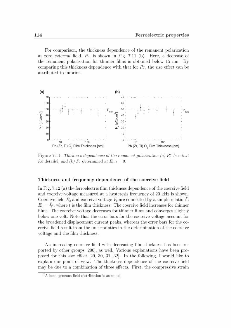
114 Ferroelectric properties
For comparison, the thickness dependence of the remanent polarizationat zero external field, Pr, is shown in Fig. 7.11 (b). Here, a decrease ofthe remanent polarization for thinner films is obtained below 15 nm. Bycomparing this thickness dependence with that for P ∗
r , the size effect can beattributed to imprint.
10 1000
10
20
30
40
50
60
70
Pbulk
Pr*
[µ
C/c
m2]
Pb (Zr, Ti) O3 Film Thickness [nm]
(a) (b)
10 1000
10
20
30
40
50
60
70
Pbulk
Pr [
µC
/cm
2]
Pb (Zr, Ti) O3 Film Thickness [nm]
Figure 7.11: Thickness dependence of the remanent polarization (a) P ∗r (see text
for details), and (b) Pr determined at Eext = 0.
Thickness and frequency dependence of the coercive field
In Fig. 7.12 (a) the ferroelectric film thickness dependence of the coercive fieldand coercive voltage measured at a hysteresis frequency of 20 kHz is shown.Coercive field Ec and coercive voltage Vc are connected by a simple relation7:Ec = Vc
t, where t is the film thickness. The coercive field increases for thinner
films. The coercive voltage decreases for thinner films and converges slightlybelow one volt. Note that the error bars for the coercive voltage account forthe broadened displacement current peaks, whereas the error bars for the co-ercive field result from the uncertainties in the determination of the coercivevoltage and the film thickness.
An increasing coercive field with decreasing film thickness has been re-ported by other groups [200], as well. Various explanations have been pro-posed for this size effect [29, 30, 31, 32]. In the following, I would like toexplain our point of view. The thickness dependence of the coercive fieldmay be due to a combination of three effects. First, the compressive strain
7A homogeneous field distribution is assumed.
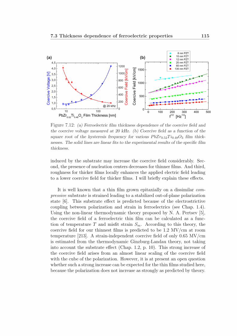
7.3 Thickness dependence of ferroelectric properties 115
(a) (b)
10 1000,5
1,0
1,5
2,0
2,5
3,0
3,5
4,0
4,5
0
200
400
600
800
1000
1200
PbZr0.52
Ti0.48
O3 Film Thickness [nm]
Coerc
ive F
ield
[kV
/cm
]
@ 20 kHz
Coerc
ive V
oltage [V
]
0 100 200 300 400 5000
500
1000
1500
8 nm PZT
10 nm PZT
12 nm PZT
20 nm PZT
60 nm PZT
135 nm PZT
Coerc
ive F
ield
[kV
/cm
]
f1/2
[Hz1/2
]
Figure 7.12: (a) Ferroelectric film thickness dependence of the coercive field and
the coercive voltage measured at 20 kHz. (b) Coercive field as a function of the
square root of the hysteresis frequency for various PbZr0.52Ti0.48O3 film thick-
nesses. The solid lines are linear fits to the experimental results of the specific film
thickness.
induced by the substrate may increase the coercive field considerably. Sec-ond, the presence of nucleation centers decreases for thinner films. And third,roughness for thicker films locally enhances the applied electric field leadingto a lower coercive field for thicker films. I will briefly explain these effects.
It is well known that a thin film grown epitaxially on a dissimilar com-pressive substrate is strained leading to a stabilized out-of-plane polarizationstate [6]. This substrate effect is predicted because of the electrostrictivecoupling between polarization and strain in ferroelectrics (see Chap. 1.4).Using the non-linear thermodynamic theory proposed by N. A. Pertsev [5],the coercive field of a ferroelectric thin film can be calculated as a func-tion of temperature T and misfit strain Sm. According to this theory, thecoercive field for our thinnest films is predicted to be 1.2 MV/cm at roomtemperature [213]. A strain-independent coercive field of only 0.65 MV/cmis estimated from the thermodynamic Ginzburg-Landau theory, not takinginto account the substrate effect (Chap. 1.2, p. 10). This strong increase ofthe coercive field arises from an almost linear scaling of the coercive fieldwith the cube of the polarization. However, it is at present an open questionwhether such a strong increase can be expected for the thin films studied here,because the polarization does not increase as strongly as predicted by theory.
116 Ferroelectric properties
Our second idea is based on the fact that the polarization reversal via cre-ation and growth of nucleation centers is energetically favorable compared tothe simultaneous switching of a single domain. Therefore, the density of nu-cleation centers determines the coercive field, and the coercive field increaseswith a decreasing nucleation center density. Defects in perovskites8 may actas pinning centers. Such pinning centers may act as nucleation centers, andthus decrease the electric field necessary to switch the polarization. Basedon high-resolution TEM and TEM investigations, our thinner films show asmaller defect density compared to thicker films [216]. As a result, a highercoercive field may be due to the presence of less nucleation centers in thinnerfilms.
Finally, the reduced coercive field can also be attributed to a larger surfaceroughness obtained for thicker films. AFM measurements show very smoothsurfaces for thinner films, e.g. an rms roughness of only 2.5 A is achieved fora 4 nm thick PbZr0.52Ti0.48O3 film. In contrast, thicker films show a roughersurface. For example, an rms roughness of 9 A is obtained for a 25 nm thickfilm. As it was discussed above, surface roughness is very likely to lead to areduced coercive field due to locally enhanced electric fields, where nucleationof domains with reversed polarization may take place at reduced externallyapplied electric fields.
The thickness dependence of the coercive field in Fig. 7.12 (a) has beendetermined at a hysteresis frequency of 20 kHz. In Fig. 7.12 (b) the coercivefield as a function of the square root of the hysteresis frequency is shownfor various ferroelectric film thicknesses. The model of Ishibashi discussed inChap. 1.2, p. 13, predicts a power law Ec = f 1/2. The experimental resultsperfectly fit this model, which is based on the Kolmogorv-Avrami model, forall investigated thicknesses and all applied hysteresis frequencies.
Current response of a 6 nm thick PbZr0.52Ti0.48O3 film
It has been mentioned that capacitors with a PbZr0.52Ti0.48O3 thicknessranging from 6 nm to 250 nm were prepared. So far, capacitors with filmthicknesses down to 8 nm have been shown and discussed. In Fig. 7.13 (b)the current response for the 6 nm sample is shown. Numbers from 1 to 8and arrows indicate the direction of scan. For comparison the already knowncurrent response for the 8 nm sample is shown in Fig. 7.13 (a). The current
8Perovskites are known for their large defect density of about 108−109 cm−2 [214, 215].
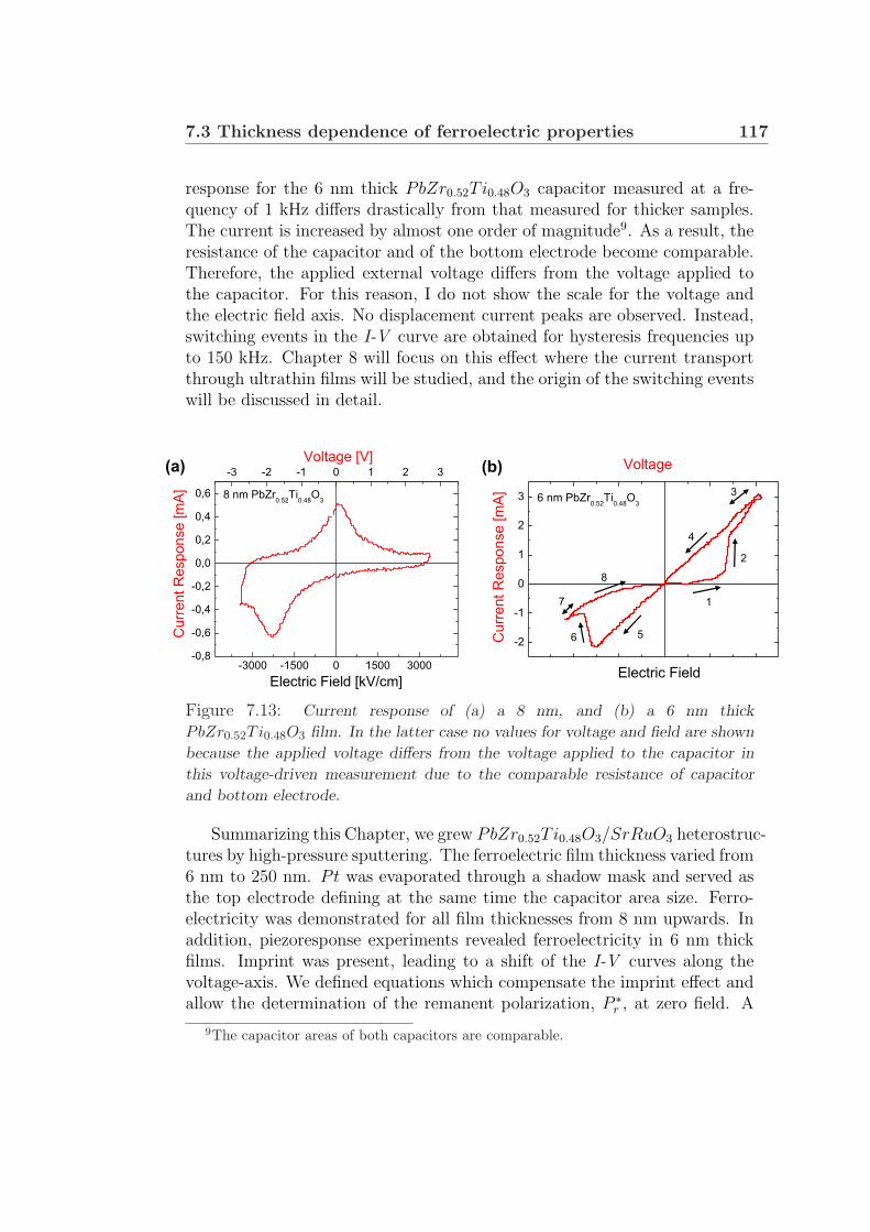
7.3 Thickness dependence of ferroelectric properties 117
response for the 6 nm thick PbZr0.52Ti0.48O3 capacitor measured at a fre-quency of 1 kHz differs drastically from that measured for thicker samples.The current is increased by almost one order of magnitude9. As a result, theresistance of the capacitor and of the bottom electrode become comparable.Therefore, the applied external voltage differs from the voltage applied tothe capacitor. For this reason, I do not show the scale for the voltage andthe electric field axis. No displacement current peaks are observed. Instead,switching events in the I-V curve are obtained for hysteresis frequencies upto 150 kHz. Chapter 8 will focus on this effect where the current transportthrough ultrathin films will be studied, and the origin of the switching eventswill be discussed in detail.
(b)
-3000 -1500 0 1500 3000-0,8
-0,6
-0,4
-0,2
0,0
0,2
0,4
0,6
-3 -2 -1 0 1 2 3
Voltage [V]
8 nm PbZr0.52
Ti0.48
O3
Curr
ent R
esponse [m
A]
Electric Field [kV/cm]
-2
-1
0
1
2
3 6 nm PbZr0.52
Ti0.48
O3
Electric Field
Curr
ent R
esponse [m
A]
Voltage(a)
1
2
3
4
56
7
8
Figure 7.13: Current response of (a) a 8 nm, and (b) a 6 nm thick
PbZr0.52Ti0.48O3 film. In the latter case no values for voltage and field are shown
because the applied voltage differs from the voltage applied to the capacitor in
this voltage-driven measurement due to the comparable resistance of capacitor
and bottom electrode.
Summarizing this Chapter, we grew PbZr0.52Ti0.48O3/SrRuO3 heterostruc-tures by high-pressure sputtering. The ferroelectric film thickness varied from6 nm to 250 nm. Pt was evaporated through a shadow mask and served asthe top electrode defining at the same time the capacitor area size. Ferro-electricity was demonstrated for all film thicknesses from 8 nm upwards. Inaddition, piezoresponse experiments revealed ferroelectricity in 6 nm thickfilms. Imprint was present, leading to a shift of the I-V curves along thevoltage-axis. We defined equations which compensate the imprint effect andallow the determination of the remanent polarization, P ∗
r , at zero field. A
9The capacitor areas of both capacitors are comparable.
118 Ferroelectric properties
nearly constant value for P ∗r was obtained for film thicknesses ranging from
10 nm to 250 nm. Remarkably, this remanent polarization corresponds to thespontaneous polarization of a stress-free bulk PbZr0.52Ti0.48O3 crystal. Thepredicted strain-induced increase of the polarization is not observed. This isattributed to the compensation by the surface effect. Besides, the coercivefield increases for decreasing film thickness. Various possible explanationshave been given for this size effect. The hysteresis frequency-coercive fieldrelation agrees with the model of Ishibashi discussed in Chap. 1.2. Switchingevents in the current response were observed for the 6 nm thick film at hys-teresis frequencies up to 150 kHz. These switching events will be discussedin detail in the following Chapter.
Chapter 8
Current transport throughultrathin films
Compared to the fabrication of capacitors described in Chap. 7, a morecomplex process has been applied to pattern tunnel junctions. In total,three photo mask steps define tunnel junctions by conventional photolithog-raphy and ion beam etching [80, 136]. First Pt/PbZr0.52Ti0.48O3/SrRuO3
or Pt/SrRuO3/BaT iO3/SrRuO3 heterostructures with a ferroelectric bar-rier thickness between 3 nm and 6 nm are Ar-etched to define the shape ofthe bottom electrode (Fig. 8.1 (a)). Rectangular junctions with areas be-tween 4 µm2 and 200 µm2 are formed by the use of a second photo maskand ion milling step, timed to end at the top surface of the bottom electrode(Fig. 8.1 (b)). The surroundings of the mesas are insulated by a 200 nmthick SiO2 layer deposited by rf-magnetron sputtering using a self-alignedprocess (Fig. 8.1 (c)). After lift-off, the third photo mask step determinesthe wiring layer, which provides an electrical contact to the top electrodeof the tunnel junction (Fig. 8.1 (d)). In addition to 45 tunnel junctions,three 100×100 µm2 crossovers without tunnel junctions serve as test struc-tures to measure the insulation resistance of the SiO2 film. The resistanceof these structures always exceeded 10 MΩ. Therefore, possible parallel cur-rent paths through the insulating SiO2 layer were neglected in the tunnelingmeasurements. In Fig. 8.1 (e), the top view of a tunnel junction includingthe current-voltage lead in a four-point arrangement is shown schematically.This arrangement eliminates the lead resistances.

120 Current transport through ultrathin films
Ar+ Ar+
V-
I+
V+
I-
Tunneling area
Photo resist PbZr0.52Ti0.48O3 SrRuO3 SrTiO3 substrate SiO2Pt
(a)
(c)
(b)
(d)
(e)
Figure 8.1: Patterning of tunnel junctions shown schematically for
Pt/PbZr0.52Ti0.48O3/SrRuO3 heterostructures. An analogous process was used
for BaTiO3-based heterostructures. See text for details.
8.1 Resistive switching effects in I-V curves
Junctions with ultrathin high-pressure sputtered PbZr0.52Ti0.48O3 and pulsedlaser ablated BaTiO3 barriers ranging from 3 nm to 6 nm were fabricated. Allmeasurements shown below were performed with a battery-powered currentsource, although in all graphs the current is plotted as a function of thevoltage. This is done in order to be consistent with the standard I-V curves.All curves shown in this Chapter are reproducible. Qualitatively similarresults are obtained for both materials studied in this work. Therefore, the
figures presented here can be regarded as valid for both materials.
Fig. 8.2 (a) shows a typical I-V characteristic of a 6 nm thick BaTiO3
film recorded at 260 K. A complete cycle lasted 10 minutes (f ≈ 1.7 mHz).Numbers from 1 to 7 and arrows show the direction of scan. Simultane-ously, the applied voltage dependence of the dynamic conductance dI/dVwas measured with a lock-in amplifier Fig. 8.2 (b). The parabolic behaviorof the dynamic conductance is indicative of electron tunneling through aninsulator. One cycle is composed of the red and the green curve. In thefollowing, I will refer to the red curve as the low-resistance curve and to thegreen curve as the high-resistance curve.
The I-V curve displays clear switching events at V −switching = −0.56 V
and V +switching = 0.84 V, and a crossover at the origin. The switching is
highly reproducible even after several I-V cycles. The resistance ratio of thehigh-resistance (3.8 kΩ) and the low-resistance (0.9 kΩ) curve at the origin
8.1 Resistive switching effects in I-V curves 121
is about 4. The asymmetry in the I-V curve for positive and negative bias-currents may be caused by different barrier heights of the top and bottomelectrode-barrier interfaces.1 Remember that an asymmetry (shift along theE-axis) was observed in thick-film capacitors as well (see Chapter 7.3).
Figure 8.2 (c) demonstrates the history effect. Prior to the measurement,a negative current pulse, corresponding to a negative electric voltage, wasapplied. The applied current is then increased from 0 mA to the maximumvalue, and decreased back to 0 mA (solid line). The direction of scan, per-formed in a quasi-static regime, is indicated by numbers and arrows. Initiallythe voltage increases along the high-resistance curve (1). At a defined valuefor the voltage a sudden decrease of the voltage from the high-resistance tothe low-resistance curve takes place (2). As the current is further increasedthe I-V characteristic moves along the low-resistance curve (3). Then thecurrent is reduced to 0 mA (4). This cycle is repeated, but this time with-out applying a negative current prior to the measurement. Only a slighthysteresis is obtained along the low-resistance curve (5). The first scan isnot reproduced unless a sufficiently negative current is applied exceeding thecritical voltage V −
switching.
The critical voltage (and field) for the switching from the high-resistanceto the low-resistance curve V +
switching (and E+switching), marked in Fig 8.2 (c)
by an arrow and a cross, was determined for temperatures between 125 Kand 300 K. In Fig. 8.2 (d) the temperature dependence of V +
switching (and
E+switching) is shown. A slight increase of the critical field for decreasing tem-
perature indicates a thermally-assisted switching.
With decreasing temperature the negative electric field increases, whichis needed to switch to the high-resistance curve. At 100 K an electric fieldof approximately 2.5 MV/cm deteriorates the junction.2 This happened toother tunnel junctions as well. Therefore, we never measured a whole I-Vcycle at temperatures below 125 K. However, the low-resistance and the high-resistance curve could be measured separately down to 4.2 K by switchingto the respective state at higher temperatures.
The dashed line in Fig. 8.3 (a) shows the I-V curve of a 4 nm thickPbZr0.52Ti0.48O3 film for an applied bias-current corresponding to an electric
1The bottom and top electrodes are both SrRuO3. Nevertheless, different structuralproperties were found for them [183].
2Note that J. Desu reported on a breakdown field in BaTiO3 of 4 MV/cm [62].
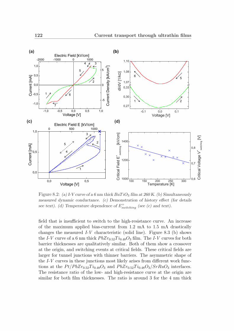
122 Current transport through ultrathin films
0,0 0,5
0,0
0,5
1,0
Curr
ent [m
A]
Voltage [V]
0 500 1000
Electric Field E [kV/cm]
-1,0 -0,5 0,0 0,5 1,0
-1,0
-0,5
0,0
0,5
1,0
-2000 -1000 0 1000
-5
0
5
Curr
ent D
ensity [kA
/cm
2]
Electric Field [kV/cm]
Curr
ent [m
A]
Voltage [V]-0,1 0,0 0,1
0,27
0,30
0,33
1,07
1,08
1,10
dI/dV
[1/k
Ω]
Voltage [V]
(a)
(c) (d)
100 150 200 250 3001000
1200
1400
0,6
0,7
0,8
Critical V
oltage V
+
sw
itch
ing [V
]
Critical F
ield
E+
sw
itch
ing [kV
/cm
]
Temperature [K]
1
2
34
5
6
7
65
21
1
2
3
4
5
(b)
Figure 8.2: (a) I-V curve of a 6 nm thick BaTiO3 film at 260 K. (b) Simultaneously
measured dynamic conductance. (c) Demonstration of history effect (for details
see text). (d) Temperature dependence of E+switching (see (c) and text).
field that is insufficient to switch to the high-resistance curve. An increaseof the maximum applied bias-current from 1.2 mA to 1.5 mA drasticallychanges the measured I-V characteristic (solid line). Figure 8.3 (b) showsthe I-V curve of a 6 nm thick PbZr0.52Ti0.48O3 film. The I-V curves for bothbarrier thicknesses are qualitatively similar. Both of them show a crossoverat the origin, and switching events at critical fields. These critical fields arelarger for tunnel junctions with thinner barriers. The asymmetric shape ofthe I-V curves in these junctions most likely arises from different work func-tions at the Pt/PbZr0.52Ti0.48O3 and PbZr0.52Ti0.48O3/SrRuO3 interfaces.The resistance ratio of the low- and high-resistance curve at the origin aresimilar for both film thicknesses. The ratio is around 3 for the 4 nm thick
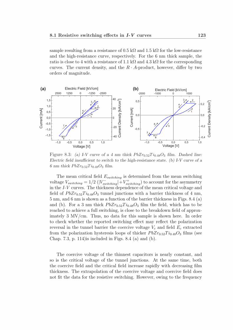
8.1 Resistive switching effects in I-V curves 123
sample resulting from a resistance of 0.5 kΩ and 1.5 kΩ for the low-resistanceand the high-resistance curve, respectively. For the 6 nm thick sample, theratio is close to 4 with a resistance of 1.1 kΩ and 4.3 kΩ for the correspondingcurves. The current density, and the R · A-product, however, differ by twoorders of magnitude.
-1,0 -0,5 0,0 0,5 1,0
-1,5
-1,0
-0,5
0,0
0,5
1,0
1,5
-40
-20
0
20
40
Curr
ent D
ensity
[kA
/cm
2]
Electric Field [kV/cm]
Curr
ent [m
A]
Voltage [V]
2500 1250 0 -1250 -2500
-1,0 -0,5 0,0 0,5 1,0
-0,5
0,0
0,5
-2000 -1000 0 1000
-0,4
-0,2
0,0
0,2
Curr
ent D
ensity [kA
/cm
2]
Electric Field [kV/cm]
Curr
ent [m
A]
Voltage [V]
(a) (b)
1
1
2
23
3
4
4
5
6
578
6
7
Figure 8.3: (a) I-V curve of a 4 nm thick PbZr0.52Ti0.48O3 film. Dashed line:
Electric field insufficient to switch to the high-resistance state. (b) I-V curve of a
6 nm thick PbZr0.52Ti0.48O3 film.
The mean critical field Eswitching is determined from the mean switchingvoltage Vswitching = 1/2 (|V −
switching|+V +switching) to account for the asymmetry
in the I-V curves. The thickness dependence of the mean critical voltage andfield of PbZr0.52Ti0.48O3 tunnel junctions with a barrier thickness of 4 nm,5 nm, and 6 nm is shown as a function of the barrier thickness in Figs. 8.4 (a)and (b). For a 3 nm thick PbZr0.52Ti0.48O3 film the field, which has to bereached to achieve a full switching, is close to the breakdown field of approx-imately 3 MV/cm. Thus, no data for this sample is shown here. In orderto check whether the reported switching effect may reflect the polarizationreversal in the tunnel barrier the coercive voltage Vc and field Ec extractedfrom the polarization hysteresis loops of thicker PbZr0.52Ti0.48O3 films (seeChap. 7.3, p. 114)is included in Figs. 8.4 (a) and (b).
The coercive voltage of the thinnest capacitors is nearly constant, andso is the critical voltage of the tunnel junctions. At the same time, boththe coercive field and the critical field increase rapidly with decreasing filmthickness. The extrapolation of the coercive voltage and coercive field doesnot fit the data for the resistive switching. However, owing to the frequency
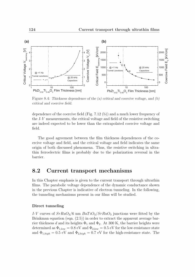
124 Current transport through ultrathin films
1 10 100
0
500
1000
1500
2000
0
500
1000
1500
2000
Tunnel Junctions Capacitors
Coerc
ive F
ield
EC [kV
/cm
]
@ <1 Hz @ 20 kHz
PbZr0.52
Ti0.48
O3 Film Thickness [nm]
Critical F
ield
ES
witch
ing [kV
/cm
]
(a) (b)
1 10 1000
1
2
3
4
0
1
2
3
4
Capacitors
Tunnel Junctions
Coerc
ive V
oltage V
C [V
]PbZr
0.52Ti
0.48O
3 Film Thickness [nm]
@ <1 Hz
@ 20 kHz
Critical V
oltage V
Sw
itch
ing [V
]
Figure 8.4: Thickness dependence of the (a) critical and coercive voltage, and (b)
critical and coercive field.
dependence of the coercive field (Fig. 7.12 (b)) and a much lower frequency ofthe I-V measurements, the critical voltage and field of the resistive switchingare indeed expected to be lower than the extrapolated coercive voltage andfield.
The good agreement between the film thickness dependences of the co-ercive voltage and field, and the critical voltage and field indicates the sameorigin of both discussed phenomena. Thus, the resistive switching in ultra-thin ferroelectric films is probably due to the polarization reversal in thebarrier.
8.2 Current transport mechanisms
In this Chapter emphasis is given to the current transport through ultrathinfilms. The parabolic voltage dependence of the dynamic conductance shownin the previous Chapter is indicative of electron tunneling. In the following,the tunneling mechanisms present in our films will be studied.
Direct tunneling
I-V curves of SrRuO3/6 nm BaTiO3/SrRuO3 junctions were fitted by theBrinkman equation (eqn. (2.5)) in order to extract the apparent average bar-rier thickness d and its heights Φ1 and Φ2. At 300 K, the barrier heights weredetermined as Φ1,low = 0.8 eV and Φ2,low = 0.5 eV for the low-resistance stateand Φ1,high = 0.5 eV and Φ2,high = 0.7 eV for the high-resistance state. The
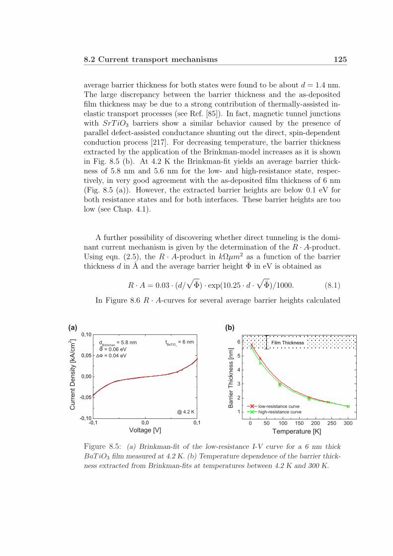
8.2 Current transport mechanisms 125
average barrier thickness for both states were found to be about d = 1.4 nm.The large discrepancy between the barrier thickness and the as-depositedfilm thickness may be due to a strong contribution of thermally-assisted in-elastic transport processes (see Ref. [85]). In fact, magnetic tunnel junctionswith SrT iO3 barriers show a similar behavior caused by the presence ofparallel defect-assisted conductance shunting out the direct, spin-dependentconduction process [217]. For decreasing temperature, the barrier thicknessextracted by the application of the Brinkman-model increases as it is shownin Fig. 8.5 (b). At 4.2 K the Brinkman-fit yields an average barrier thick-ness of 5.8 nm and 5.6 nm for the low- and high-resistance state, respec-tively, in very good agreement with the as-deposited film thickness of 6 nm(Fig. 8.5 (a)). However, the extracted barrier heights are below 0.1 eV forboth resistance states and for both interfaces. These barrier heights are toolow (see Chap. 4.1).
A further possibility of discovering whether direct tunneling is the domi-nant current mechanism is given by the determination of the R ·A-product.Using eqn. (2.5), the R · A-product in kΩµm2 as a function of the barrierthickness d in A and the average barrier height Φ in eV is obtained as
R · A = 0.03 · (d/√
Φ) · exp(10.25 · d ·√
Φ)/1000. (8.1)
In Figure 8.6 R · A-curves for several average barrier heights calculated
-0,1 0,0 0,1-0,10
-0,05
0,00
0,05
0,10
@ 4.2 K
tBaTiO
3
= 6 nm dBrinkman
= 5.8 nm
Φ = 0.06 eV
∆Φ = 0.04 eV
Curr
ent D
ensity [kA
/cm
2]
Voltage [V]0 50 100 150 200 250 300
1
2
3
4
5
6
low-resistance curve
high-resistance curve
Barr
ier
Thic
kness [
nm
]
Temperature [K]
(a) (b)
Film Thickness
Figure 8.5: (a) Brinkman-fit of the low-resistance I-V curve for a 6 nm thick
BaTiO3 film measured at 4.2 K. (b) Temperature dependence of the barrier thick-
ness extracted from Brinkman-fits at temperatures between 4.2 K and 300 K.
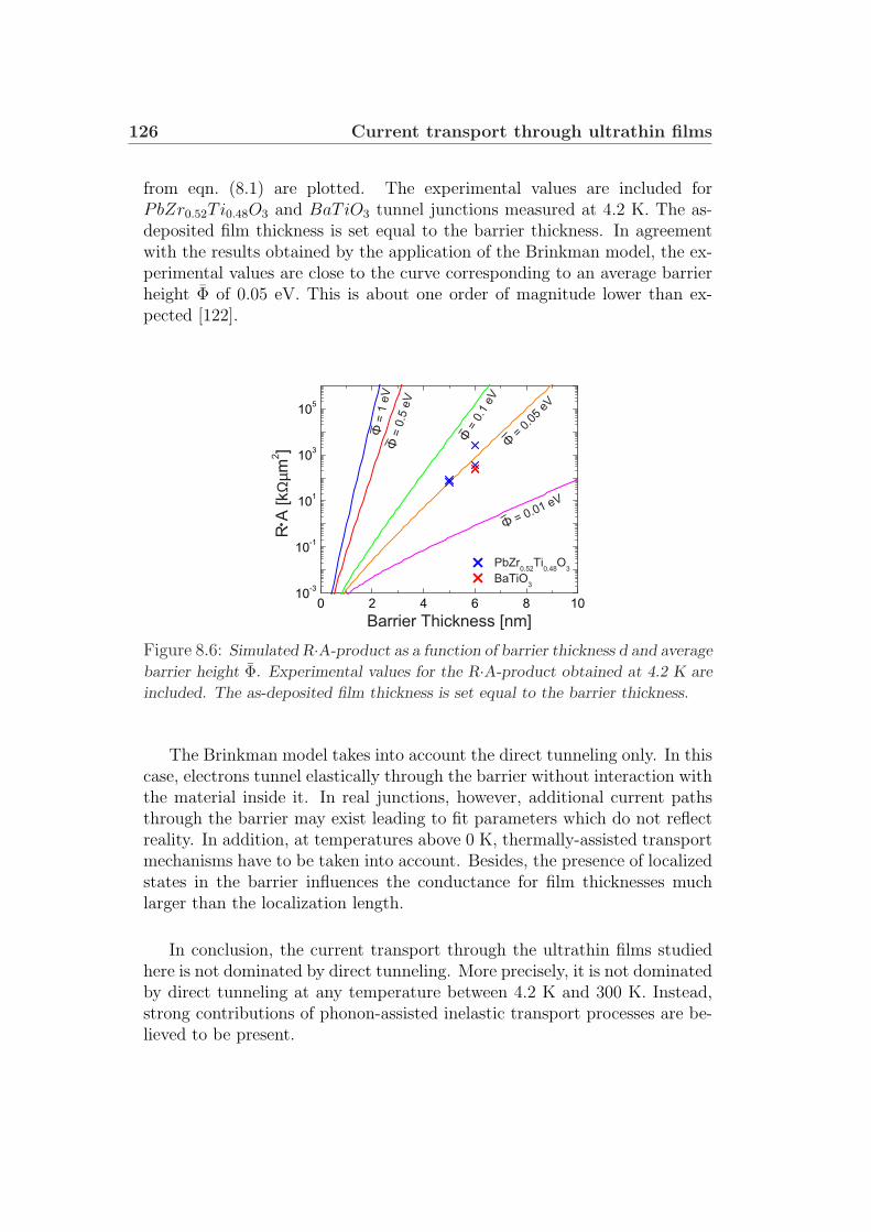
126 Current transport through ultrathin films
from eqn. (8.1) are plotted. The experimental values are included forPbZr0.52Ti0.48O3 and BaTiO3 tunnel junctions measured at 4.2 K. The as-deposited film thickness is set equal to the barrier thickness. In agreementwith the results obtained by the application of the Brinkman model, the ex-perimental values are close to the curve corresponding to an average barrierheight Φ of 0.05 eV. This is about one order of magnitude lower than ex-pected [122].
0 2 4 6 8 1010
-3
10-1
101
103
105
Φ=
1eV
Φ=
0.5
eV
Φ=
0.1
eV
Φ = 0
.05
eV
Φ = 0.01 eV
Barrier Thickness [nm]
R A
[k
Ωµm
2]
PbZr0.52
Ti0.48
O3
BaTiO3
Figure 8.6: Simulated R·A-product as a function of barrier thickness d and average
barrier height Φ. Experimental values for the R·A-product obtained at 4.2 K are
included. The as-deposited film thickness is set equal to the barrier thickness.
The Brinkman model takes into account the direct tunneling only. In thiscase, electrons tunnel elastically through the barrier without interaction withthe material inside it. In real junctions, however, additional current pathsthrough the barrier may exist leading to fit parameters which do not reflectreality. In addition, at temperatures above 0 K, thermally-assisted transportmechanisms have to be taken into account. Besides, the presence of localizedstates in the barrier influences the conductance for film thicknesses muchlarger than the localization length.
In conclusion, the current transport through the ultrathin films studiedhere is not dominated by direct tunneling. More precisely, it is not dominatedby direct tunneling at any temperature between 4.2 K and 300 K. Instead,strong contributions of phonon-assisted inelastic transport processes are be-lieved to be present.
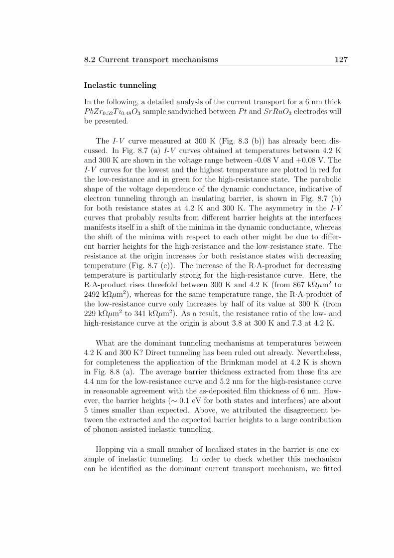
8.2 Current transport mechanisms 127
Inelastic tunneling
In the following, a detailed analysis of the current transport for a 6 nm thickPbZr0.52Ti0.48O3 sample sandwiched between Pt and SrRuO3 electrodes willbe presented.
The I-V curve measured at 300 K (Fig. 8.3 (b)) has already been dis-cussed. In Fig. 8.7 (a) I-V curves obtained at temperatures between 4.2 Kand 300 K are shown in the voltage range between -0.08 V and +0.08 V. TheI-V curves for the lowest and the highest temperature are plotted in red forthe low-resistance and in green for the high-resistance state. The parabolicshape of the voltage dependence of the dynamic conductance, indicative ofelectron tunneling through an insulating barrier, is shown in Fig. 8.7 (b)for both resistance states at 4.2 K and 300 K. The asymmetry in the I-Vcurves that probably results from different barrier heights at the interfacesmanifests itself in a shift of the minima in the dynamic conductance, whereasthe shift of the minima with respect to each other might be due to differ-ent barrier heights for the high-resistance and the low-resistance state. Theresistance at the origin increases for both resistance states with decreasingtemperature (Fig. 8.7 (c)). The increase of the R·A-product for decreasingtemperature is particularly strong for the high-resistance curve. Here, theR·A-product rises threefold between 300 K and 4.2 K (from 867 kΩµm2 to2492 kΩµm2), whereas for the same temperature range, the R·A-product ofthe low-resistance curve only increases by half of its value at 300 K (from229 kΩµm2 to 341 kΩµm2). As a result, the resistance ratio of the low- andhigh-resistance curve at the origin is about 3.8 at 300 K and 7.3 at 4.2 K.
What are the dominant tunneling mechanisms at temperatures between4.2 K and 300 K? Direct tunneling has been ruled out already. Nevertheless,for completeness the application of the Brinkman model at 4.2 K is shownin Fig. 8.8 (a). The average barrier thickness extracted from these fits are4.4 nm for the low-resistance curve and 5.2 nm for the high-resistance curvein reasonable agreement with the as-deposited film thickness of 6 nm. How-ever, the barrier heights (∼ 0.1 eV for both states and interfaces) are about5 times smaller than expected. Above, we attributed the disagreement be-tween the extracted and the expected barrier heights to a large contributionof phonon-assisted inelastic tunneling.
Hopping via a small number of localized states in the barrier is one ex-ample of inelastic tunneling. In order to check whether this mechanismcan be identified as the dominant current transport mechanism, we fitted
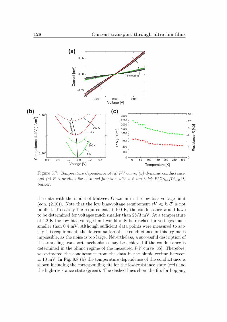
128 Current transport through ultrathin films
0 50 100 150 200 250 3000
100
200
300
1000
1500
2000
2500
3000R
A [k
Ωµm
2]
Temperature [K]
0
1
4
8
12
16
Resis
tance R
[k
Ω]
-0,05 0,00 0,05
-0,05
0,00
0,05
T increasingC
urr
ent [m
A]
Voltage [V]
(a)
(b) (c)
-0,6 -0,4 -0,2 0,0 0,2 0,4
5x10⁵
5x10⁶
Tin
cre
asin
g 5 K
5 K
300 K
300 K
Conducta
nce d
J/d
V [1/Ω
m2]
Voltage [V]
Figure 8.7: Temperature dependence of (a) I-V curve, (b) dynamic conductance,
and (c) R·A-product for a tunnel junction with a 6 nm thick PbZr0.52Ti0.48O3
barrier.
the data with the model of Matveev-Glazman in the low bias-voltage limit(eqn. (2.10)). Note that the low bias-voltage requirement eV ¿ kBT is notfulfilled. To satisfy the requirement at 100 K, the conductance would haveto be determined for voltages much smaller than 25/3 mV. At a temperatureof 4.2 K the low bias-voltage limit would only be reached for voltages muchsmaller than 0.4 mV. Although sufficient data points were measured to sat-isfy this requirement, the determination of the conductance in this regime isimpossible, as the noise is too large. Nevertheless, a successful description ofthe tunneling transport mechanisms may be achieved if the conductance isdetermined in the ohmic regime of the measured I-V curve [85]. Therefore,we extracted the conductance from the data in the ohmic regime between± 10 mV. In Fig. 8.8 (b) the temperature dependence of the conductance isshown including the corresponding fits for the low-resistance state (red) andthe high-resistance state (green). The dashed lines show the fits for hopping
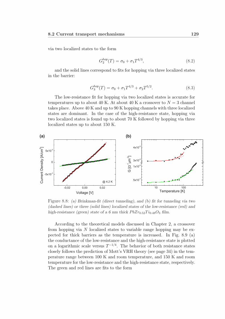
8.2 Current transport mechanisms 129
via two localized states to the form
Ghop2 (T ) = σ0 + σ1T
4/3, (8.2)
and the solid lines correspond to fits for hopping via three localized statesin the barrier:
Ghop3 (T ) = σ0 + σ1T
4/3 + σ2T5/2. (8.3)
The low-resistance fit for hopping via two localized states is accurate fortemperatures up to about 40 K. At about 40 K a crossover to N = 3 channeltakes place. Above 40 K and up to 90 K hopping channels with three localizedstates are dominant. In the case of the high-resistance state, hopping viatwo localized states is found up to about 70 K followed by hopping via threelocalized states up to about 150 K.
-0,02 0,00 0,02
-5x10⁻³
0
5x10⁻³
@ 4.2 KCurr
ent D
ensity [A
/cm
2]
Voltage [V]
(a) (b)
10 100
5x10⁻⁷
1x10⁻⁶
3x10⁻⁶
4x10⁻⁶
G [
Ω-1
µm-2]
Temperature [K]
Figure 8.8: (a) Brinkman-fit (direct tunneling), and (b) fit for tunneling via two
(dashed lines) or three (solid lines) localized states of the low-resistance (red) and
high-resistance (green) state of a 6 nm thick PbZr0.52Ti0.48O3 film.
According to the theoretical models discussed in Chapter 2, a crossoverfrom hopping via N localized states to variable range hopping may be ex-pected for thick barriers as the temperature is increased. In Fig. 8.9 (a)the conductance of the low-resistance and the high-resistance state is plottedon a logarithmic scale versus T−1/4. The behavior of both resistance statesclosely follows the prediction of Mott’s VRH theory (see page 34) in the tem-perature range between 100 K and room temperature, and 150 K and roomtemperature for the low-resistance and the high-resistance state, respectively.The green and red lines are fits to the form
130 Current transport through ultrathin films
GV RH = GV RH0 · exp
(−
( T
T
)1/4). (8.4)
Fig. 8.9 (b) is a logarithmic plot of the current density versus E−1/4. Thedata is fitted to Shklovskii’s model
JV RH = JV RH0 · exp
(−
( E
E
)1/4). (8.5)
The Shklovskii model (see page 34) precisely fits the data in the highbias-voltage regime (eV À kBT ) of both the low-resistance and the high-resistance curve.
0,2 0,3 0,4
5x10⁻⁷
5x10⁻⁶ 100 K
VRH
150 K300 K
VRH
G [
Ω-1
µm-2]
T-1/4
[K-1/4
]
0,040 0,045 0,050
0,01
0,1
@ 4.2 KCurr
ent D
ensity [kA
/cm
2]
E-1/4
[(V/cm)-1/4
]
(a) (b)
Figure 8.9: Application of (a) Mott’s law, and (b) Shklovskii’s model to the low-
resistance (red) and high-resistance (green) state of a 6 nm thick PbZr0.52Ti0.48O3
film.
In conclusion, the electron tunneling theories developed for amorphousmaterials have been applied to our single-crystalline thin films. Those theo-ries are believed to be applicable to perovskite materials, due to their largedefect density (see Chapter 2). We have demonstrated that the currenttransport through the studied PbZr0.52Ti0.48O3 and BaTiO3 barriers withfilm thicknesses between 4 nm and 6 nm is dominated by phonon-assistedinelastic tunneling processes for all temperatures between 4.2 K and 300 K.We have analyzed in detail the current transport mechanisms through a 6 nmthick PbZr0.52Ti0.48O3 film. For the low-resistance curve, hopping via two
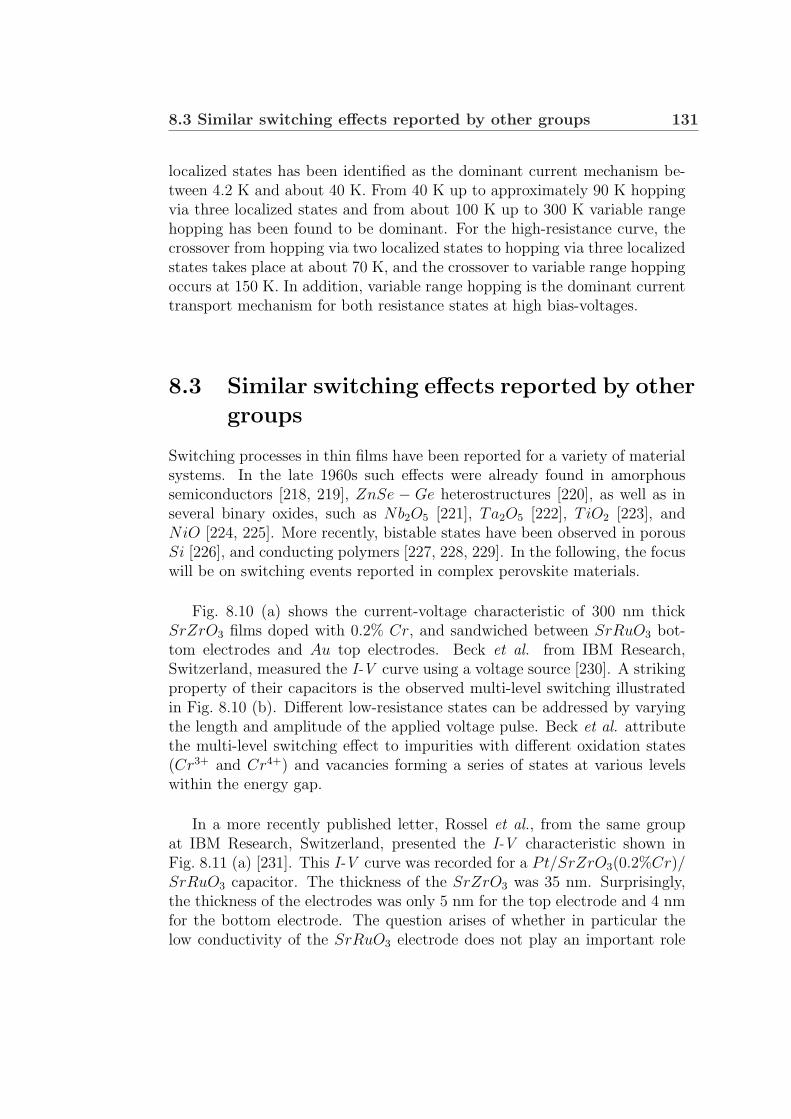
8.3 Similar switching effects reported by other groups 131
localized states has been identified as the dominant current mechanism be-tween 4.2 K and about 40 K. From 40 K up to approximately 90 K hoppingvia three localized states and from about 100 K up to 300 K variable rangehopping has been found to be dominant. For the high-resistance curve, thecrossover from hopping via two localized states to hopping via three localizedstates takes place at about 70 K, and the crossover to variable range hoppingoccurs at 150 K. In addition, variable range hopping is the dominant currenttransport mechanism for both resistance states at high bias-voltages.
8.3 Similar switching effects reported by other
groups
Switching processes in thin films have been reported for a variety of materialsystems. In the late 1960s such effects were already found in amorphoussemiconductors [218, 219], ZnSe − Ge heterostructures [220], as well as inseveral binary oxides, such as Nb2O5 [221], Ta2O5 [222], TiO2 [223], andNiO [224, 225]. More recently, bistable states have been observed in porousSi [226], and conducting polymers [227, 228, 229]. In the following, the focuswill be on switching events reported in complex perovskite materials.
Fig. 8.10 (a) shows the current-voltage characteristic of 300 nm thickSrZrO3 films doped with 0.2% Cr, and sandwiched between SrRuO3 bot-tom electrodes and Au top electrodes. Beck et al. from IBM Research,Switzerland, measured the I-V curve using a voltage source [230]. A strikingproperty of their capacitors is the observed multi-level switching illustratedin Fig. 8.10 (b). Different low-resistance states can be addressed by varyingthe length and amplitude of the applied voltage pulse. Beck et al. attributethe multi-level switching effect to impurities with different oxidation states(Cr3+ and Cr4+) and vacancies forming a series of states at various levelswithin the energy gap.
In a more recently published letter, Rossel et al., from the same groupat IBM Research, Switzerland, presented the I-V characteristic shown inFig. 8.11 (a) [231]. This I-V curve was recorded for a Pt/SrZrO3(0.2%Cr)/SrRuO3 capacitor. The thickness of the SrZrO3 was 35 nm. Surprisingly,the thickness of the electrodes was only 5 nm for the top electrode and 4 nmfor the bottom electrode. The question arises of whether in particular thelow conductivity of the SrRuO3 electrode does not play an important role
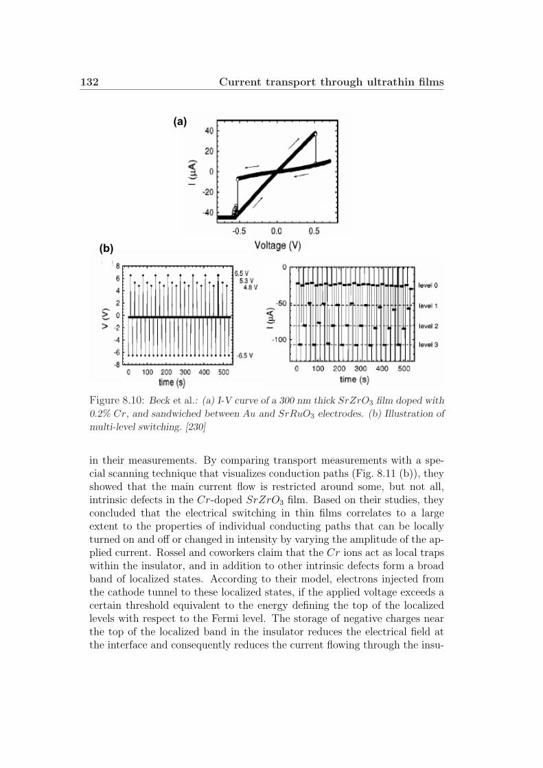
132 Current transport through ultrathin films
(a)
(b)
Figure 8.10: Beck et al.: (a) I-V curve of a 300 nm thick SrZrO3 film doped with
0.2% Cr, and sandwiched between Au and SrRuO3 electrodes. (b) Illustration of
multi-level switching. [230]
in their measurements. By comparing transport measurements with a spe-cial scanning technique that visualizes conduction paths (Fig. 8.11 (b)), theyshowed that the main current flow is restricted around some, but not all,intrinsic defects in the Cr-doped SrZrO3 film. Based on their studies, theyconcluded that the electrical switching in thin films correlates to a largeextent to the properties of individual conducting paths that can be locallyturned on and off or changed in intensity by varying the amplitude of the ap-plied current. Rossel and coworkers claim that the Cr ions act as local trapswithin the insulator, and in addition to other intrinsic defects form a broadband of localized states. According to their model, electrons injected fromthe cathode tunnel to these localized states, if the applied voltage exceeds acertain threshold equivalent to the energy defining the top of the localizedlevels with respect to the Fermi level. The storage of negative charges nearthe top of the localized band in the insulator reduces the electrical field atthe interface and consequently reduces the current flowing through the insu-
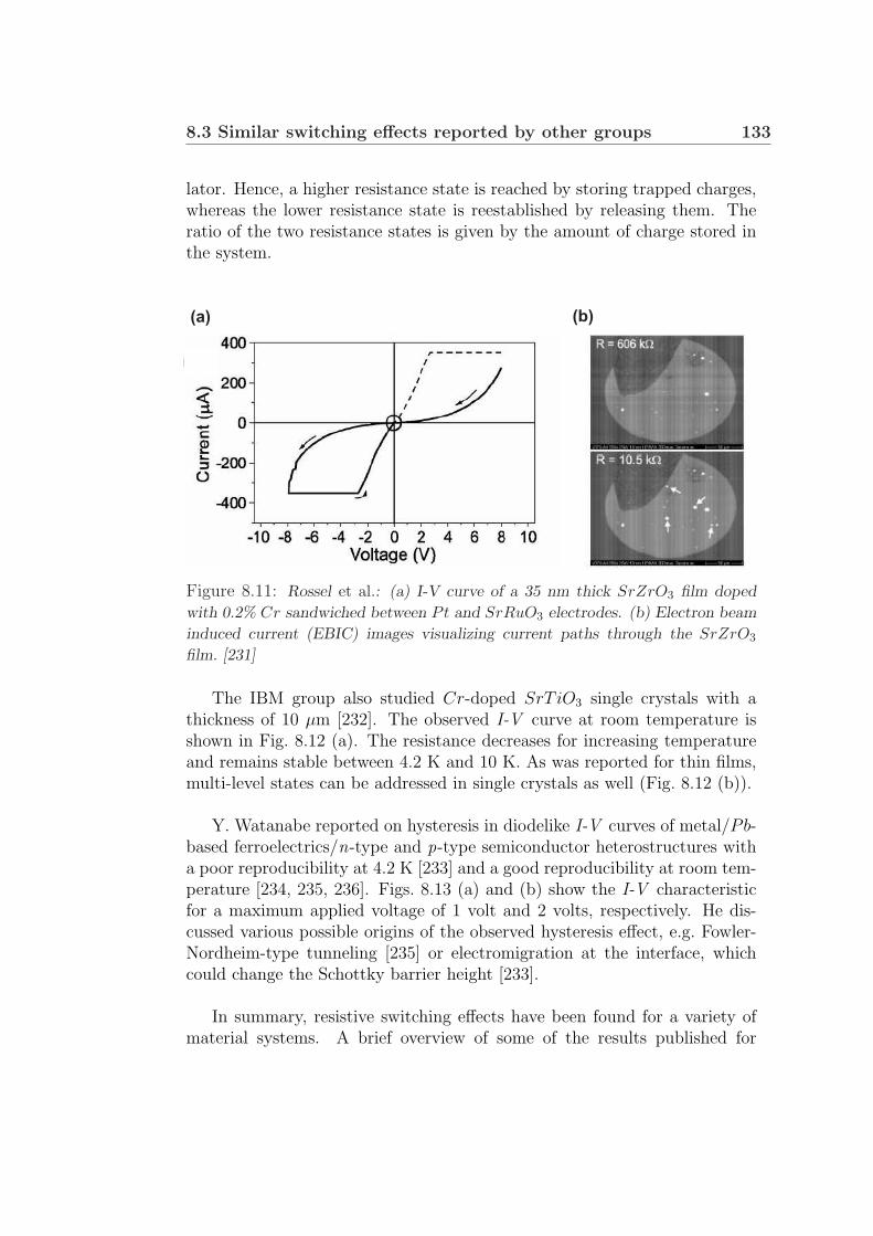
8.3 Similar switching effects reported by other groups 133
lator. Hence, a higher resistance state is reached by storing trapped charges,whereas the lower resistance state is reestablished by releasing them. Theratio of the two resistance states is given by the amount of charge stored inthe system.
(a) (b)
Figure 8.11: Rossel et al.: (a) I-V curve of a 35 nm thick SrZrO3 film doped
with 0.2% Cr sandwiched between Pt and SrRuO3 electrodes. (b) Electron beam
induced current (EBIC) images visualizing current paths through the SrZrO3
film. [231]
The IBM group also studied Cr-doped SrT iO3 single crystals with athickness of 10 µm [232]. The observed I-V curve at room temperature isshown in Fig. 8.12 (a). The resistance decreases for increasing temperatureand remains stable between 4.2 K and 10 K. As was reported for thin films,multi-level states can be addressed in single crystals as well (Fig. 8.12 (b)).
Y. Watanabe reported on hysteresis in diodelike I-V curves of metal/Pb-based ferroelectrics/n-type and p-type semiconductor heterostructures witha poor reproducibility at 4.2 K [233] and a good reproducibility at room tem-perature [234, 235, 236]. Figs. 8.13 (a) and (b) show the I-V characteristicfor a maximum applied voltage of 1 volt and 2 volts, respectively. He dis-cussed various possible origins of the observed hysteresis effect, e.g. Fowler-Nordheim-type tunneling [235] or electromigration at the interface, whichcould change the Schottky barrier height [233].
In summary, resistive switching effects have been found for a variety ofmaterial systems. A brief overview of some of the results published for

134 Current transport through ultrathin films
(a) (b)
Figure 8.12: Watanabe and coworkers at IBM Zurich: (a) I-V curve recorded at
296 K on a SrT iO3 : Cr single crystal. (b) Multiple low-resistance states obtained
at 4.5 K after write pulses (N) with different current amplitudes of 1.5, 2.2, 2.5,
2.7, 3.0, 3.5 mA and erase pulses (¤) with a fixed amplitude of -3.55 mA. Each
pulse is followed by 1000 readouts at −0.5 V . [232]
perovskite materials has been given in this Chapter. Particularly the I-Vcharacteristics obtained by the IBM group show some interesting similaritieswith the current-voltage curves reported in this PhD thesis. Nevertheless,we do believe that the current transport and the origin of the switching ef-fects are different. We base our assumption on the following distinctions:First, the thickness of our films is smaller by at least one order of magni-tude. Besides, the switching effects presented in Chap. 8.1 for 4 nm to 6 nmthick PbZr0.52Ti0.48O3 and BaTiO3 films were not observed for 12 nm thickbarriers. I-V curves recorded for junctions with this thickness showed non-reproducible jumps or hysteresis in the I-V characteristic at much highervoltages, most likely due to a deterioration of the ferroelectric film. Sec-ond, we do not find multi-level resistance states in our junctions. And fi-nally, the temperature dependence of the resistance, which decreases withdecreasing temperature, differs from that measured for tunnel junctions withPbZr0.52Ti0.48O3 or BaTiO3 barriers, where the resistance increases withdecreasing temperature.
8.4 Final remarks on resistive switching and
current transport mechanisms
The thickness dependence of the coercive voltage (and coercive field) forthick-film capacitors can be extrapolated to ultrathin films. Taking into ac-
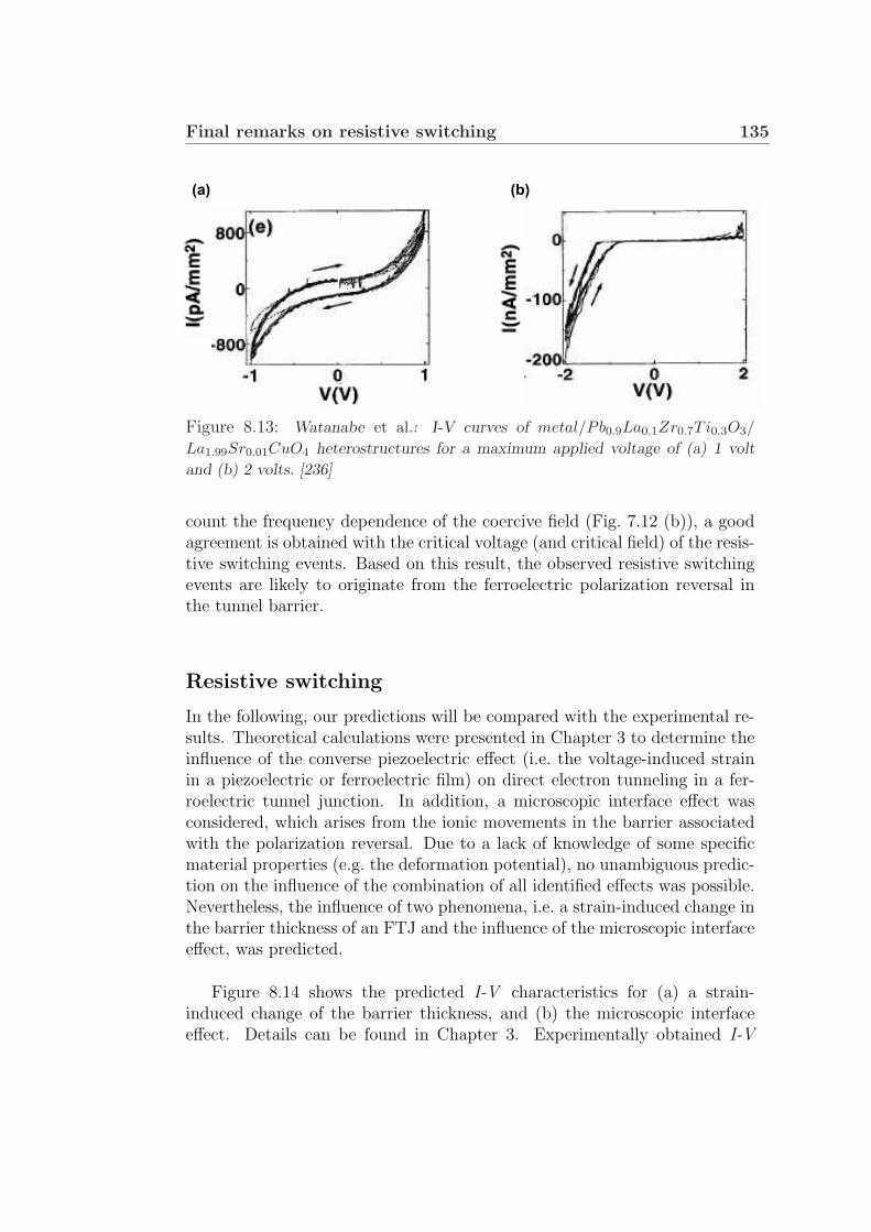
Final remarks on resistive switching 135
(a) (b)
Figure 8.13: Watanabe et al.: I-V curves of metal/Pb0.9La0.1Zr0.7Ti0.3O3/
La1.99Sr0.01CuO4 heterostructures for a maximum applied voltage of (a) 1 volt
and (b) 2 volts. [236]
count the frequency dependence of the coercive field (Fig. 7.12 (b)), a goodagreement is obtained with the critical voltage (and critical field) of the resis-tive switching events. Based on this result, the observed resistive switchingevents are likely to originate from the ferroelectric polarization reversal inthe tunnel barrier.
Resistive switching
In the following, our predictions will be compared with the experimental re-sults. Theoretical calculations were presented in Chapter 3 to determine theinfluence of the converse piezoelectric effect (i.e. the voltage-induced strainin a piezoelectric or ferroelectric film) on direct electron tunneling in a fer-roelectric tunnel junction. In addition, a microscopic interface effect wasconsidered, which arises from the ionic movements in the barrier associatedwith the polarization reversal. Due to a lack of knowledge of some specificmaterial properties (e.g. the deformation potential), no unambiguous predic-tion on the influence of the combination of all identified effects was possible.Nevertheless, the influence of two phenomena, i.e. a strain-induced change inthe barrier thickness of an FTJ and the influence of the microscopic interfaceeffect, was predicted.
Figure 8.14 shows the predicted I-V characteristics for (a) a strain-induced change of the barrier thickness, and (b) the microscopic interfaceeffect. Details can be found in Chapter 3. Experimentally obtained I-V
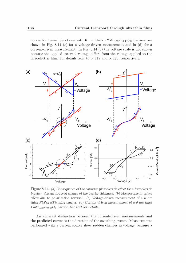
136 Current transport through ultrathin films
curves for tunnel junctions with 6 nm thick PbZr0.52Ti0.48O3 barriers areshown in Fig. 8.14 (c) for a voltage-driven measurement and in (d) for acurrent-driven measurement. In Fig. 8.14 (c) the voltage scale is not shownbecause the applied external voltage differs from the voltage applied to theferroelectric film. For details refer to p. 117 and p. 123, respectively.
-1,0 -0,5 0,0 0,5 1,0
-0,5
0,0
0,5
-0,4
-0,2
0,0
0,2
Curr
ent D
ensity [kA
/cm
2]
Curr
ent
[mA
]
Voltage [V]
1
23
4
58
6
7
-2
-1
0
1
2
3
Voltage
Curr
ent [m
A]
1
2
3
4
56
7
8
d -d 0
Voltage
Voltage
I
(a)
Vc-Vc
-Vc Vc
Voltage
I
-Vc Vc
Voltage-Vc
Vc
P(b)
(c) (d)
Figure 8.14: (a) Consequence of the converse piezoelectric effect for a ferroelectric
barrier: Voltage-induced change of the barrier thickness. (b) Microscopic interface
effect due to polarization reversal. (c) Voltage-driven measurement of a 6 nm
thick PbZr0.52Ti0.48O3 barrier. (d) Current-driven measurement of a 6 nm thick
PbZr0.52Ti0.48O3 barrier. See text for details.
An apparent distinction between the current-driven measurements andthe predicted curves is the direction of the switching events. Measurementsperformed with a current source show sudden changes in voltage, because a
Final remarks on resistive switching 137
current source supplies a predetermined current. Hence, the voltage-drivenand current-driven measurements are in agreement with the predictions withrespect to the direction of the switching events.
The I-V curves for the strain-induced change of the barrier thickness andthe microscopic interface effect both show a step-like reduction of the conduc-tance at ±Vc. However, such a reduction is not present in the experimentalcurves at V +
switching.
The most striking difference between predicted and observed I-V curvesis their behavior at the origin (marked by circles in Figs. 8.14 (a) and (c)).A crossover is observed in the experiments in disagreement with the predic-tions. Thus, the symmetry of the I-V characteristics is different. It shouldbe noted that the predicted symmetry is a characteristic feature for all effectsarising from the piezoelectric effect (e.g. strain-induced shift of the conduc-tance and valence band edges).
In conclusion, some features are identical for the predicted and the ex-perimentally observed I-V characteristics. However, the observed switch-ing events in the I-V curves cannot be exclusively explained by either theconverse piezoelectric effect, or by a change of the barrier heights of themetal-ferroelectric and the ferroelectric-metal interfaces. Especially the dif-ferent symmetry of the predicted and the measured curves demonstrates thatfurther research is necessary to unambiguously verify the nature of the ob-served resistive switching effects. At present, it is an open question whetherthe observed distinctions may be associated with further manifestations offerroelectricity or caused by additional effects not related to ferroelectricity.
Current transport mechanisms
In order to simplify the theoretical study, an elastic current transport mech-anism is desirable. In fact, direct electron tunneling was assumed for thetheoretical treatment of ferroelectricity and electron tunneling presented inChapter 3. The presence of inelastic transport processes may lead to addi-tional, superimposed effects, which might be larger than those discussed fordirect tunneling.
In our tunnel junctions with PbZr0.52Ti0.48O3 and BaTiO3 barriers, in-elastic current transport mechanisms are dominant for all investigated barrierthicknesses and all temperatures between 4.2 K and room temperature. Di-
138 Current transport through ultrathin films
rect electron tunneling is probably achievable for a barrier thickness belowtwo nm. Moran et al. studied the current transport for tunnel junctions witha SrT iO3 barrier thickness ranging from 2 nm to 20 nm [82, 83]. They ob-served elastic tunneling, but only for a barrier thickness of nominally 2 nm.Even for slightly thicker SrT iO3 barriers, tunneling and hopping via a smallnumber of localized states dominated the transport behavior. SrT iO3 is aperovskite titanate like the ferroelectric materials used in this work. It thusseems straightforward to grow films with thicknesses of 2 nm and less. How-ever, the switching field for a 2 nm thick PbZr0.52Ti0.48O3 barrier, assuminga switching voltage of 0.7 V, is as large as 3.5 MV/cm. Recalling that thebreakdown field was already reached for 3 nm thick PbZr0.52Ti0.48O3 films.The breakdown in BaTiO3 films was observed for even smaller fields. Forfuture studies the use of ferroelectric materials with lower coercive fields issuggested.
Summary
The concept of a ferroelectric tunnel junction has been presented. The de-vice was termed FTJ and consists of a ferroelectric layer sandwiched betweenmetal electrodes. The ferroelectric layer has to be thin enough to allowquantum-mechanical electron tunneling.
The aim of this work was the study of a possible interaction of ferroelec-tricity and the quantum-mechanical electron tunneling through the ferroelec-tric barrier. This involved both experimental and theoretical tasks.
From the experimental point of view, the main challenge was the growthof ferroelectric films as thin as a few nm. Size effects may decrease themanifestation of ferroelectricity. They may even completely suppress ferro-electricity in sufficiently thin films. Hence, the first step was the selection ofthe appropriate material system yielding favorable boundary conditions withthe ultimate goal of stabilizing the ferroelectric phase.
In this thesis, we primarily studied the heterostructures of Pt/PbZr0.52Ti0.48O3/SrRuO3 and SrRuO3/BaT iO3/SrRuO3, both grown onSrT iO3 (100) substrates. Three different deposition techniques were used,namely high-pressure sputtering, molecular beam epitaxy, and pulsed laserdeposition. For the characterization and optimization of the thin films,various analytical methods were utilized, among them XRD, RBS, AFM,HRTEM, and RHEED (for MBE-grown thin films).
Compressive strain is induced in the ferroelectric PbZr0.52Ti0.48O3 and(Ba, Sr)TiO3 thin films by the SrT iO3 substrate due to its smaller in-planelattice parameter. This substrate effect is an opponent of the surface effect,which tends to decrease the polarization in subsurface layers. On the otherhand, it has to be taken into account that too much strain leads to strainrelief via generation of misfit dislocations. First, very promising results wereobtained on the novel substrate material, DyScO3. This substrate provides a

140 Summary
perfect lattice match for the growth of SrRuO3 thin films, which we used asa bottom electrode. In comparison with SrT iO3, the in-plane lattice param-eters of DyScO3 are slightly larger. This reduces the compressive strain inoxide perovskite materials, such as PbZr0.52Ti0.48O3 and BaTiO3. Thus, itsuse as substrate material is expected to increase the critical film thickness forthe introduction of strain-releasing defects. The conducting oxide perovskiteSrRuO3 was employed as the bottom electrode due to its good structural andchemical compatibility with SrT iO3 and the ferroelectrics used. Remarkably,we were able to grow SrRuO3 exhibiting an even smoother surface than thebare SrT iO3 substrate. Needless to say, a smooth surface leading to a sharpinterface between the electrode and the barrier is a strong requirement forthe successful preparation of a tunnel junction with a barrier consisting ofa few monolayers. The most frequently studied ferroelectric perovskite wasemployed in the composition PbZr0.52Ti0.48O3 because it combines a largespontaneous polarization with the strongest piezoelectric effect. The secondferroelectric material studied within this work was BaTiO3. Its main ad-vantage compared to PbZr0.52Ti0.48O3 is the smaller lattice mismatch withthe SrRuO3/SrT iO3 heterostructure allowing for a thicker ferroelectric filmwithout misfit dislocations. So far, only mechanical boundary conditionshave been considered. However, electrical boundary conditions are impor-tant as well. For example, the use of SrRuO3 as top electrode material forPbZr0.52Ti0.48O3-based capacitors resulted in an extrinsic size effect. We at-tributed this size effect to increased leakage currents due to a smaller barrierheight at the SrRuO3/PbZr0.52Ti0.48O3 interface in comparison to the bar-rier height at the Pt/PbZr0.52Ti0.48O3 interface. In contrast, the oppositeobservation for BaTiO3 thin films, i.e. higher leakage currents in the case ofPt top electrodes, remains unexplained.
Once the growth techniques were well established, and the material sys-tems were selected, the ferroelectric properties of thick-film capacitors ofprogressively shrinking film thickness could be studied. It was of particularinterest to determine both the thickness dependence of the remanent po-larization and the thickness dependence of the coercive field. The purposeof doing this can be stated as follows. First, the observation of a ferro-electric hysteresis loop with a non-zero remanent polarization demonstratesthe presence of ferroelectricity in the film. Besides, PbZr0.52Ti0.48O3 andstrained BaTiO3 films are predicted to undergo a second-order phase tran-sition from the ferroelectric to the paraelectric phase. Thus a continuouschange of the polarization may be expected. Therefore, its thickness depen-dence yields information about the stability of the ferroelectric phase. Andsecond, typical analytical methods fail to detect ferroelectricity in ultrathin
Summary 141
films, although they might be ferroelectric. Instead, knowledge of the thick-ness dependence of the coercive field can be used to extrapolate the coercivefield for an ultrathin ferroelectric film, which serves as barrier in a FTJ. Westarted by growing 250 nm thick PbZr0.52Ti0.48O3 films and 100 nm thickBaTiO3 films. A nearly constant remanent polarization was observed forboth ferroelectric materials studied, i.e. for PbZr0.52Ti0.48O3 films in a filmthickness range between 250 nm and 10 nm and BaTiO3 films with a thick-ness ranging from 100 nm to 12 nm. Remarkably, the value for the remanentpolarization in PbZr0.52Ti0.48O3 thin films was identical to the spontaneouspolarization of a stress-free bulk single crystal for this composition. Based onthis result, we concluded that either no intrinsic size effect is present for thisthickness range, or the intrinsic size effect is compensated by the substrateeffect. A further proof, showing that the ferroelectric phase in a 10 nm thickPbZr0.52Ti0.48O3 film is still far from losing the stability, was the observationof ferroelectric polarization reversals at 300C. In fact, ferroelectricity wasdemonstrated in 8 nm thick films, and piezoresponse force microscopy ex-periments revealed ferroelectricity even in 6 nm thick PbZr0.52Ti0.48O3 films.This is already a thickness regime in which electron tunneling may be ob-served. Hence, the study of thick-film capacitors with the ultimate goal ofensuring ferroelectricity in ultrathin tunnel barriers was successful. The sec-ond important result was the determination of the coercive voltage, whichwas constant for the thinnest PbZr0.52Ti0.48O3 thin films. At the same time,the coercive field was increasing for thinner films.
The optimization of thin-film growth conditions typically takes a longtime and does not provide much entertainment. This is the best time todevelop some theoretical ideas on what might be expected if we succeeded inmeasuring a tunneling current through a ferroelectric barrier.
From a fundamental point of view, direct electron tunneling is the onlycurrent transport mechanism present in a metal-insulator-metal structureat 0 K. Chapter 3 of this thesis deals with the term, which describes thetunneling probability for direct electron tunneling. In collaboration withN. A. Pertsev, we identified and predicted various interactions of the con-verse piezoelectric effect and the ferroelectric polarization reversal with directelectron tunneling. In the following, I will briefly summarize these effects.
The converse piezoelectric effect, i.e. the linear voltage dependence of thestrain in a piezoelectric material, leads to three strain-induced effects, each ofwhich alters the tunneling probability. First, a strain-induced change of thebarrier thickness. Second, a strain-induced change of the effective mass of the
142 Summary
electrons in the barrier arising from a change of the lattice parameters. Andthird, a strain-induced shift of the valence and conduction band edges. Dueto a lack of knowledge of some specific material properties, no unambiguousprediction on the influence of the combination of all three identified strain-induced effects was possible. In fact, it is likely that the first two effectsmentioned and the latter effect partially compensate each other. Neverthe-less, it seems very unlikely that they could compensate each other exactly.Irrespective of this uncertainty, a current-voltage characteristic was calcu-lated taking into account a strain-induced change in the barrier thickness ofa FTJ. Using typical values for PbZr0.52Ti0.48O3, considerable effects wereobtained. The features characterizing this strain-induced thickness variationwere a sudden change of the tunneling current at the coercive field of thebarrier material, and a shift of the minima in the dynamic conductance withrespect to each other and with respect to the origin.
In addition to the converse piezoelectric effect, the idea was discussedthat the microscopic manifestation of the polarization reversal, i.e. a changein the atomic structure, may change the barrier potential. Surprisingly, theI-V curve for the simulation of this effect is characterized by the same mainfeatures as obtained above for the strain-induced change of the barrier thick-ness. Despite these similarities, both effects are independent of each other.
After significant experimental improvements, we were able to grow thinfilms exhibiting ferroelectric properties at a film thickness, which can be re-garded as an upper limit for electron tunneling. At the same time, we hadspeculated, what the I-V curves for a FTJ might look like. So, it was abouttime to start the fabrication of ferroelectric tunnel junctions.
Tunnel junctions with PbZr0.52Ti0.48O3 and BaTiO3 barriers were suc-cessfully prepared with a thickness of the barrier ranging from 4 nm to 6 nm.The I-V curves displayed clear switching events at well defined electric fieldsand a crossover at the origin. The switching was highly reproducible andwas observed at frequencies ranging from 10−4 Hz to 106 Hz. At room tem-perature, the resistance ratio of the high-resistance and the low-resistancecurves at the origin was typically around 4. This ratio was increased forlower temperatures, and it was around 8 at 4.2 K.
An extrapolation of the thickness dependence of the coercive voltage toultrathin films revealed a good agreement between the resistive switchingeffects in tunnel junctions and the ferroelectric polarization reversal in thick-film capacitors. Based on this result, the resistive switching in ultrathin
Summary 143
ferroelectric films is likely to be the consequence of the polarization reversalin the barrier.
A comparison with the theoretical concepts stated above yielded identicalfeatures for the predicted and the experimentally observed I-V characteris-tics. However, other experimentally observed features, e.g. the direction ofthe switching events and the crossover at the origin, did not agree with thepredictions. Hence, the observed switching events in the I-V curves cannotbe exclusively explained by either the converse piezoelectric effect, or by achange of the barrier heights of the metal-ferroelectric and the ferroelectric-metal interfaces. At present, it is an open question, whether the observeddistinctions may be associated with further manifestations of ferroelectricityor caused by additional, superimposed effects not related to ferroelectricity.
Finally, the current transport mechanisms through the FTJ barriers werestudied. The current transport was found to be dominated by phonon-assisted inelastic tunneling processes for all temperatures between 4.2 K and300 K. We analyzed a 6 nm thick PbZr0.52Ti0.48O3 barrier in detail. For thelow-resistance curve, hopping via two localized states was identified as thedominant current transport mechanism between 4.2 K and about 40 K. From40 K up to approximately 90 K hopping via three localized states and fromabout 100 K up to 300 K variable range hopping was found to be dominant.For the high-resistance curve, the crossover from hopping via two localizedstates to hopping via three localized states took place at about 70 K, andthe crossover to variable range hopping occurred at 150 K. In addition, vari-able range hopping was the dominant current mechanism for both resistancestates at high bias-voltages.
Outlook
It would be highly desirable, if a current transport mechanism dominatedsolely by electron tunneling could be realized. This would simplify the inves-tigation of the interaction of ferroelectricity and tunneling through a ferro-electric barrier. A barrier thickness between 4 nm and 6 nm is too thick toachieve pure direct electron tunneling. To that end, a barrier thickness notgreater than 2 nm is required [82, 83]. Low-magnification TEM in combina-tion with high-resolution TEM verified the homogeneous and, based on theresolution limit of this technique, defect-free growth of 2 nm thick BaTiO3
films. However, the expected coercive voltage for this film thickness exceeds

144 Summary
the breakdown field. Therefore, for future studies the use of ferroelectricmaterials, such as Zr-rich PbZrxTi1−xO3 with lower coercive fields [111] issuggested.
A different approach could be the fabrication of tunnel junctions with aSrT iO3 barrier grown on a sufficiently compressive substrate. The advan-tages of this barrier material over the well-established ferroelectric materials,Pb(Zr, T i)O3 and BaTiO3, are the following. First, direct electron tunnelingthrough SrT iO3 barriers has already been demonstrated for a film thicknessof 2 nm. Second, the strain-induced paraelectric to ferroelectric phase tran-sition temperature is expected to be well below room temperature providinga small coercive field in the ferroelectric phase (see eqn. (1.20)). And finally,a low phase transition temperature allows the measurement of I-V curvesbelow TC and above TC . A resistive switching in the ferroelectric state andno switching effect in the paraelectric state could be taken as an unambigu-ous proof of a ferroelectric origin of the resistive switching.
Bibliography
Introduction
[1] L. E. Cross and R. E. Newnham, in Ceramics and Civilization,Vol. III, High Technology Ceramics - Past, Present, and Future, (ed.W. D. Kingery, American Ceramic Society, Columbus, OH), 1987
[2] I. P. Batra and B. D. Silverman, Solid State Commun. Vol. 11,291, 1972
[3] P. Wurfel and I. P. Batra, Ferroelectrics Vol. 12, 55, 1976
[4] R. Kretschmer and K. Binder, Phys. Rev. Vol. B20 (3), 1065,1979
[5] N. A. Pertsev, A. G. Zembilgotov, and A. K. Tagantsev,Phys. Rev. Lett. Vol. 80, 1988, 1998
[6] A. G. Zembilgotov, N. A. Pertsev, H. Kohlstedt, and R.Waser, J. Appl. Phys. Vol. 91 (4), 2247, 2002
[7] J. Junquera and Ph. Ghosez, Nature Vol. 422, 506, 2003
[8] N. Yanase, K. Abe, N. Fukushima, and T. Kawakubo, Jpn.J. Appl. Phys. Vol. 38, 5305, 1999
[9] T. Tybell, C. H. Ahn, and J.-M. Triscone, Appl. Phys. Lett.Vol. 75, 856, 1999
[10] S. Streiffer, J. A. Eastman, D. D. Fong, C. Thompson, A.Munkholm, M. V. Ramana Murty, O. Auciello, G. R. Bai,G. B. Stephenson, Phys. Rev. Lett. Vol. 89 (6), 067601, 2002
[11] D. D. Fong, G. B. Stephenson, S. K. Streiffer, J. A. East-man, O. Auciello, P. H. Fuoss, C. Thompson, submitted toNature
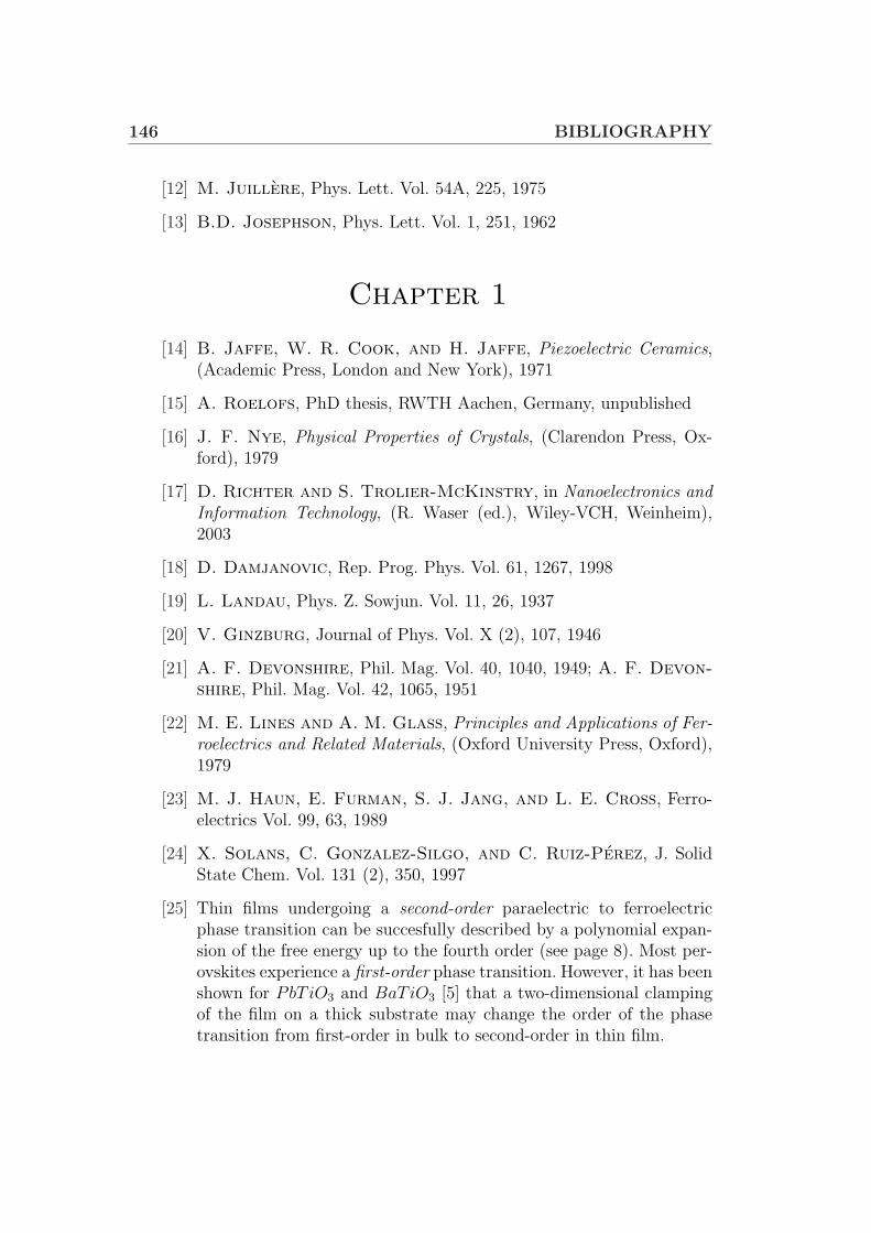
146 BIBLIOGRAPHY
[12] M. Juillere, Phys. Lett. Vol. 54A, 225, 1975
[13] B.D. Josephson, Phys. Lett. Vol. 1, 251, 1962
Chapter 1
[14] B. Jaffe, W. R. Cook, and H. Jaffe, Piezoelectric Ceramics,(Academic Press, London and New York), 1971
[15] A. Roelofs, PhD thesis, RWTH Aachen, Germany, unpublished
[16] J. F. Nye, Physical Properties of Crystals, (Clarendon Press, Ox-ford), 1979
[17] D. Richter and S. Trolier-McKinstry, in Nanoelectronics andInformation Technology, (R. Waser (ed.), Wiley-VCH, Weinheim),2003
[18] D. Damjanovic, Rep. Prog. Phys. Vol. 61, 1267, 1998
[19] L. Landau, Phys. Z. Sowjun. Vol. 11, 26, 1937
[20] V. Ginzburg, Journal of Phys. Vol. X (2), 107, 1946
[21] A. F. Devonshire, Phil. Mag. Vol. 40, 1040, 1949; A. F. Devon-shire, Phil. Mag. Vol. 42, 1065, 1951
[22] M. E. Lines and A. M. Glass, Principles and Applications of Fer-roelectrics and Related Materials, (Oxford University Press, Oxford),1979
[23] M. J. Haun, E. Furman, S. J. Jang, and L. E. Cross, Ferro-electrics Vol. 99, 63, 1989
[24] X. Solans, C. Gonzalez-Silgo, and C. Ruiz-Perez, J. SolidState Chem. Vol. 131 (2), 350, 1997
[25] Thin films undergoing a second-order paraelectric to ferroelectricphase transition can be succesfully described by a polynomial expan-sion of the free energy up to the fourth order (see page 8). Most per-ovskites experience a first-order phase transition. However, it has beenshown for PbT iO3 and BaTiO3 [5] that a two-dimensional clampingof the film on a thick substrate may change the order of the phasetransition from first-order in bulk to second-order in thin film.
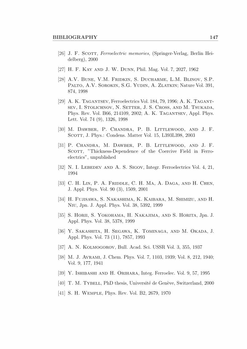
BIBLIOGRAPHY 147
[26] J. F. Scott, Ferroelectric memories, (Springer-Verlag, Berlin Hei-delberg), 2000
[27] H. F. Kay and J. W. Dunn, Phil. Mag. Vol. 7, 2027, 1962
[28] A.V. Bune, V.M. Fridkin, S. Ducharme, L.M. Blinov, S.P.Palto, A.V. Sorokin, S.G. Yudin, A. Zlatkin; Nature Vol. 391,874, 1998
[29] A. K. Tagantsev, Ferroelectrics Vol. 184, 79, 1996; A. K. Tagant-sev, I. Stolichnov, N. Setter, J. S. Cross, and M. Tsukada,Phys. Rev. Vol. B66, 214109, 2002; A. K. Tagantsev, Appl. Phys.Lett. Vol. 74 (9), 1326, 1998
[30] M. Dawber, P. Chandra, P. B. Littlewood, and J. F.Scott, J. Phys.: Condens. Matter Vol. 15, L393L398, 2003
[31] P. Chandra, M. Dawber, P. B. Littlewood, and J. F.Scott, ”Thickness-Dependence of the Coercive Field in Ferro-electrics”, unpublished
[32] N. I. Lebedev and A. S. Sigov, Integr. Ferroelectrics Vol. 4, 21,1994
[33] C. H. Lin, P. A. Friddle, C. H. Ma, A. Daga, and H. Chen,J. Appl. Phys. Vol. 90 (3), 1509, 2001
[34] H. Fujisawa, S. Nakashima, K. Kaibara, M. Shimizu, and H.Niu, Jpn. J. Appl. Phys. Vol. 38, 5392, 1999
[35] S. Horii, S. Yokohama, H. Nakajima, and S. Horita, Jpn. J.Appl. Phys. Vol. 38, 5378, 1999
[36] Y. Sakashita, H. Segawa, K. Tominaga, and M. Okada, J.Appl. Phys. Vol. 73 (11), 7857, 1993
[37] A. N. Kolmogorov, Bull. Acad. Sci. USSR Vol. 3, 355, 1937
[38] M. J. Avrami, J. Chem. Phys. Vol. 7, 1103, 1939; Vol. 8, 212, 1940;Vol. 9, 177, 1941
[39] Y. Ishibashi and H. Orihara, Integ. Ferroelec. Vol. 9, 57, 1995
[40] T. M. Tybell, PhD thesis, Universite de Geneve, Switzerland, 2000
[41] S. H. Wemple, Phys. Rev. Vol. B2, 2679, 1970
148 BIBLIOGRAPHY
[42] P. G. Gennes, Rev. Mod. Phys. Vol. 36, 225, 1965
[43] E. Guyon and C. D. Mitescu, Thin Solid Films Vol. 12, 355, 1972
[44] C. A. Neugebauer, Phys. Rev. Vol. 116, 1441, 1959
[45] T. Mitsui and J. Furuichi, Phys. Rev. Vol. 90, 193, 1953
[46] N. A. Pertsev, private communication
[47] V. L. Bonch-Bruevich, S. G. Kalashnikov, Halbleiterphysik,(Deutscher Verlag der Wissenschaften: Berlin), 1982
[48] P. Wurfel, I. P. Batra, and J. T. Jacobs, Phys. Rev. Lett.Vol. 30 (24), 1218, 1973
[49] I. P. Batra, P. Wurfel, and B. D. Silverman, J. Vac. Sci.Technol. Vol. 10 (5), 687, 1973
[50] I. P. Batra, P. Wurfel, and B. D. Silverman, Phys. Rev.Vol. B8 (7), 3257, 1973
[51] I. P. Batra, P. Wurfel, and B. D. Silverman, Phys. Rev. Lett.Vol. 30, 384, 1973
[52] P. Wurfel and I. P. Batra, Phys. Rev. Vol. B8 (11), 5126, 1973
[53] V. L. Vinetskii, M. A. Itskovskii, and L. S. Kremenchugskii,Sov. Phys. Sol. St. Vol. 15, 2330, 1974
[54] I. I. Ivanchik, Sov. Phys. Solid State Vol. 3 (12), 2705, 1962
[55] L. Baudry and J. Tournier, J. Appl. Phys. Vol. 90 (3), 1442,2001
[56] K. Binder, Ferroelectrics Vol. 35, 99, 1981
[57] J. F. Scott, H. M. Duiker, P. D. Beale, B. Pouligny,K. Dimmler, M. Parris, D. Butler, and S. Eaton, PhysicaVol. B150, 160, 1988
[58] D. Tilley, Ferroelectrics Vol. 134, 313, 1992
[59] D. Tilley and B. Zeks, Solid State Commun. Vol. 49, 823, 198
[60] W. L. Zhong, B. D. Qu, P. L. Zhang, and Y. G. Wang, Phys.Rev. Vol. B50 (17), 12375, 1994
BIBLIOGRAPHY 149
[61] S. Li, J. A. Eastman, J. M. Vetrone, C. M. Foster, R. E.Newnham, and L. E. Cross, Jpn. J. Appl. Phys. Vol. 36, 5169,1997
[62] S. B. Desu, J. Electrochem. Soc. Vol. 140 (10), 2981, 1993
[63] J. S. Speck and W. Pompe, J. Appl. Phys. Vol. 76 (1), 466, 1994
[64] B. S. Kwak, A. Erbil, B. J. Wilkens, J. D. Budai, M. F.Chisholm, and L. A. Boatner, Phys. Rev. Lett. Vol. 68, 3733,1992
[65] H. Kohlstedt, N. A. Pertsev, and R. Waser, Mat. Res. Soc.Symp. Proc. Vol. 688, 161, 2002
[66] N. A. Pertsev, A. G. Zembilgotov, and A. K. Tagantsev,Ferroelectrics Vol. 223, 79, 1999
[67] J. S. Zhu, X. M. Lu, P. Li, W. Jiang, and Y. N. Wang, SolidState Comm. Vol. 101 (4), 263, 1997
[68] O. Auciello, Extension of the total free energy was suggested duringthe International Symposium on Integrated Ferroelectrics (ISIF) inColorado Springs, CO, 2003
[69] Ph. Ghosez and K.M. Rabe, Appl. Phys. Lett. Vol. 76, 2767, 2000
[70] B. Meyer and D. Vanderbilt, Phys. Rev. Vol. B63, 205426, 2001
Chapter 2
[71] J. Frenkel, Phys. Rev. Vol. 36, 1604, 1930
[72] E. L. Wolf, Principles of tunneling spectroscopy, Plenum Press, p.183, 1990
[73] D. V. Geppert, J. Appl. Phys. Vol. 34, 490, 1963
[74] K. H. Gundlach, PhD thesis, Technische Universitat Clausthal,1970
[75] S. Shapiro, P. H. Smith, J. Nicol, J. L. Miles, P. F. Strong,IBM Journal Vol. 34(1), 1962

150 BIBLIOGRAPHY
[76] F. Schwabl, Quantenmechanik, 2nd ed. Springer, p. 183, 1990
[77] K. H. Gundlach, J. Appl. Phys. Vol. 44 (11), 5005, 1973
[78] J.G. Simmons, J. Appl. Phys. Vol. 35, 2655, 1964
[79] W. F. Brinkman, R. C. Dynes, and J. M. Rowell, J. Appl.Phys. Vol. 41, 1915, 1970
[80] J. Z. Sun, L. Krusin-Elbaum, P.R. Duncombe, A. Gupta,and R. B. Laibowitz, Appl. Phys. Lett. Vol. 70(13), 1769, 1997
[81] L. I. Glazman, private communication
[82] O. Moran Campana, PhD thesis, Forschungszentrum Karlsruhe,Germany, 2002
[83] O. Moran Campana, to be submitted to J. Appl. Phys
[84] C. Hofener, PhD thesis, Universitat zu Koln, Germany, 2000
[85] Y. Xu, D. Ephron, and M. R. Beasley, Physical Rev. Vol. B52(4), 1995
[86] J. Wingbermuhle, PhD thesis, Forschungszentrum Julich, Ger-many, 2002
[87] R. Stratton, J. Phys. Chem. Solids Vol. 23, 1177, 1962
[88] A. I. Larkin and K. A. Matveev, Sov. Phys. JETP Vol. 66, 580,1987
[89] Y. Xu, PhD thesis, Stanford Unisversity, USA, 1992
[90] L. I. Glazman and R. I. Shekter, Sov. Phys. JETP Vol. 67, 163,1988
[91] A. D. Stone and P. A. Lee, Phys. Rev. Lett. Vol. 54, 1196, 1985
[92] L. I. Glazman and K. A. Matveev, Sov. Phys. JETP Vol. 67,1276, 1988
[93] N. F. Mott and E. A. Davis, Electronic Processes in Non-Crystalline Materials, 2nd ed. (Oxford University Press, New York),1979
BIBLIOGRAPHY 151
[94] B. I. Shklovskii, Sov. Phys. Semicond. Vol. 6 (12), 1964, 1973
Chapter 3
[95] R. Wolf, P. W. M. Blom, and M. P. C. Krijn, TUNNELDIODE WITH SEVERAL PERMANENT SWITCHING STATES,U. S. Patent, Patent Number 5,541,422, July 30th, 1996
[96] L. Esaki, R. B. Laibowitz, and P. J. Stiles, IBM TechnicalDisclosure Bulletin Vol. 13 (8), 2161, 1971; L. L. Chang and L.Esaki, IBM Technical Disclosure Bulletin Vol. 14 (4), 1250, 1971
[97] Ch. Kittel, Introduction to Solid State Physics, 7th Ed., (Wiley,New York), 1996
[98] W. Q. Chen and S. K. Hark, J. Appl. Phys. Vol. 77 (11), 5747,1995
[99] T. B. Bahder, Phys. Rev. Vol. B41 (17), 11992, 1990; Phys. Rev.Vol. B45 (4), 1629, 1992
[100] C. G. Van de Walle, Phys. Rev. Vol. B39 (3), 1871, 1989
[101] P. Waltereit, A. E. Romanov, and J. S. Speck, Appl. Phys.Lett. Vol. 81 (25), 4757, 2002
[102] S. Ghosh, P. Waltereit, O. Brandt, H. T. Grahn, and K.H. Ploog, Phys. Rev. Vol. B65, 075202, 2002; S.-H. Park andS.-L. Chuang, J. Appl. Phys. Vol. 87 (1), 353, 2000
[103] U. Karrer, O. Ambacher, and M. Stutzmann, Appl. Phys.Lett. Vol. 77, 2012, 2000
[104] M. Stutzmann, O. Ambacher, M. Eickhoff, U. Karrer, A.Lima Pimenta, R. Neuberger, J. Schalwig, R. Dimitrov, P.j. Schuck, and R. D. Grober, Phys. Stat. Sol. Vol. 228 (2), 505,2001
[105] A. Rizzi and H. Luth, Appl. Phys. Vol. A75, 69, 2002
152 BIBLIOGRAPHY
Chapter 4
[106] J. F. Scott and C. A. Paz de Araujo, Science Vol. 246, 1400,1989
[107] D. L. Polla, C. Ye, and T. Tamagawa, Appl. Phys. Lett. Vol. 59,3539, 1991
[108] G. H. Haertling, J. Vac. Sci. Technol. Vol. A9, 414, 1991
[109] R. Aidam and R. Schneider, Thin Solid Films Vol. 384, 1, 2001
[110] J. F. M. Cillessen, M. W. J. Prins, and R. M. Wolf, J. Appl.Phys. Vol. 81 (6), 2777, 1997
[111] C. M. Foster, G.-R. Bai, R. Csencsits, J. Vetrone, R.Jammy, L. A. Wills, E. Carr, and J. Amano, J. Appl. Phys.Vol. 81 (5), 2349, 1997
[112] C. D. Theis, J. Yeh, D. G. Schlom, M. E. Hawley, and G.W. Brown, Thin Solid Films Vol. 325, 107, 1998
[113] M. J. Haun, T. R. Halemane, R. E. Newnham, and L. E.Cross, Jpn. J. Appl. Phys. Vol 24 (Supplement 24-2), 209, 1985
[114] F. Jona and G. Shirane, Ferroelectric Crystals - InternationalSeries of Monographs on Solid State Physics Vol. 1 (R. Smoluchowskiand N. Kurti (eds.), Pergamon Press, Oxford, London, New York,Paris), 1962
[115] N. A. Pertsev, V. G. Kukhar, H. Kohlstedt, and R. Waser,Phys. Rev. Vol. B67, 054107, 2003
[116] B. Noheda, D. E. Cox, G. Shirane, J. A. Gonzalo, L. E.Cross, and S.-E. Park, Appl. Phys. Lett. Vol. 74, 2059, 1999; B.Noheda, J. A. Gonzalo, L. E. Cross, R. Guo, S.-E. Park,D. E. Cox, and G. Shirane, Phys. Rev. Vol. B61, 8687, 2000; B.Noheda, D. E. Cox, G. Shirane, R. Guo, B. Jones, and L.E. Cross, Phys. Rev. Vol. B63, 014103-1, 2000
[117] L. Bellaiche, A. Garcia, and D. Vanderbilt, Phys. Rev. Lett.Vol. 84, 5427, 2000
BIBLIOGRAPHY 153
[118] D. Vanderbilt and M. H. Cohen, Phys. Rev. Vol. B63, 094108,2001
[119] L. Wu, T.-S. Wu, C.-C. Wei, and H.-C. Liu, J. Phys. Vol. C16,2823, 1983
[120] R. Gerson and H. Jaffe, J. Phys. Chem. Solids Vol. 24, 979, 1963
[121] D. K. Schroder, Semiconductor Material and Device Characteri-zation, 2nd Ed., (John Wiley & Sons, Inc., New York, Chichester,Weinheim, Brisbane, Singapore, Toronto), 1998
[122] C. Sudhama, A. C. Campbell, P. D. Maniar, R. E. Jones, R.Moazzami, C. J. Mogab, and J. C. Lee, J. Appl. Phys. Vol. 75(2), 1014, 1994
[123] A. J. Hartmann, M. Neilson, R. N. Lamb, K. Watanabe,and J. F. Scott, Appl. Phys. Vol. A70, 239, 2000
[124] A. I. Kingon, S. K. Streiffer, C. Basceri, and S. R. Sum-merfelt, MRS Bulletin, p. 46, July 1996
[125] K. Abe, N. Yanase, T. Kawakubo, Jpn. J. Appl. Phys. Vol. 40,2367, 2001; K. Abe, N. Yanase, and T. Kawakubo, Jpn. J. Appl.Phys. Vol. 39, 4059, 2000; N. Yanase, K. Abe, N. Fukushima,and T. Kawakubo, Jpn. J. Appl. Phys. Vol. 38, 5305, 1999; K.Abe and S. Komatsu, J. Appl. Phys. Vol. 77 (12), 6461, 1995
[126] J. C. Shin, J. Park, C. S. Hwang, and H. J. Kim, J. Appl.Phys. Vol. 86 (1), 506, 1999
[127] M. Siegert, J. G. Lisoni, C. H. Lei, A. Eckau, W. Zander,J. Schubert, and Ch. Buchal, Mat. Res. Soc. Proc. Vol. 597,145, 2000
[128] F. Fitsilis, S. Regnery, P. Ehrhart, R. Waser, F. Schienle,M. Schumacher, H. Juergenssen, Integr. Ferroelec. Vol. 38, 211,2001
[129] R. A. McKee, F. J. Walker, and M. F. Chisholm, ScienceVol. 293 (5529), 468, 2001; R. A. McKee, F. J. Walker, E. DSpecht, G. E. Jellison, Jr., L. A. Boatner, and J. Harding,Phys. Rev. Lett. Vol. 72 (17), 2741, 1994; R. A. McKee, F. J.Walker, J. R. Conner, and E. D Specht, Appl. Phys. Lett.Vol. 59 (7), 782, 1991
154 BIBLIOGRAPHY
[130] K. Shimoyama, K. Kubo, M. Iida, K. Yamabe, and T. Maeda,J. Vac. Sci. Technol. Vol. A19 (5), 2083,2001
[131] Y. Yoneda, T. Okabe, K. Sakaue, H. Terauchi, H. Kasa-tani, and K. Deguchi, J. Appl. Phys. Vol. 83 (5), 2458, 1998
[132] H. Shigetani, K. Kobayashi, M. Fujimoto, W. Sugimura, Y.Matsui, and J. Tanaka, J. Appl. Phys. Vol. 81 (2), 693, 1997
[133] T. Tsurumi, T. Suzuki, M. Yamane, and M. Daimon, Jpn. J.Appl. Phys. Vol. 33, 5192, 1994
[134] Gmelin Handbook of inorganic and organometallic Chem-istry, Main: Titan, Vol. 41, (Springer Verlag, New York), 1951
[135] F. Fitsilis, PhD thesis, Forschungszentrum Julich, 2002
[136] Y. Lu, X. W. Li, G. Q. Gong, G. Xiao, A. Gupta, P.Lecoeur, J. Z. Sun, Y. Y. Wang, and V. P. David, Phys.Rev. Vol. B54, 8357, 1996
[137] A. Callaghan, C. W. Moeller, and R. Ward, Inorg. Chem.Vol. 5, 1572, 1996
[138] R. J. Bouchard and J. L. Gillson, Mater. Res. Bull. Vol. 7, 873,1972
[139] A. Kanbayasi, J. Phys. Soc. Japan Vol. 44, 89, 1978
[140] J. C. Jiang and X. Q. Pan, Phil. Mag. Lett. Vol. 80 (5), 271, 2000
[141] J.-P. Maria, H. L. McKinstry, and S. Trolier-McKinstry,Appl. Phys. Lett. Vol. 76 (23), 3382, 2000
[142] B. C. Chakoumakos, S. E. Nagler, S. T. Misture, and H.M. Christen, Physica Vol. B241-243, 358, 1998
[143] C. B. Eom, R. J. Cava, R. M. Fleming, J. M. Phillips, R. B.van Dover, J. H. Marshall, J. W. P. Hsu, J. J. Krajewski,and W. F. Peck, Science Vol. 258, 1766, 1992
[144] X. D. Wu, S. R. Foltyn, R. C. Dye, Y. Coulter, and R. E.Muenchausen, Appl. Phys. Lett. Vol. 62, 2434, 1993
BIBLIOGRAPHY 155
[145] Q. X. Jia, F. Chu, C. D. Adams, X. D. Wu, M. Hawley, J.H. Cho, A. T. Findikoglu, S. R. Foltyn, J. L. Smith, andT. E. Mitchell, J. Mater. Res. Vol. 11, 2263, 1996
[146] M. Hiratani, C. Okazaki, K. Imagawa, and K. Takagi, Jpn.J. Appl. Phys. Vol. 35, 6212, 1996
[147] H. Funakubo, T. Oikawa, N. Higashi, and K. Saito, J. Cryst.Growth. Vol. 229, 450, 2001
[148] L. Klein, Y. Kats, A. F. Marshall, J. W. Reiner, T. H.Geballe, M. R. Beasley, and A. Kapitulnik, Phys. Rev. Lett.Vol. 84 (26), 6090, 2000; L. Klein, A. F. Marshall, J. W.Reiner, C. H. Ahn, T. H. Geballe, M. R. Beasley, andA. Kapitulnik, J. Magn. Magn. Mater. Vol. 188, 319, 1998; C. H.Ahn, R. H. Hammond, T. H. Geballe, M. R. Beasley, J.-M.Triscone, M. Decroux, Ø. Fischer, L. Antognazza, andK. Char, Appl. Phys. Lett. Vol. 70 (2), 206, 1996; L. Klein, J.S. Dodge, C. H. Ahn, G. J. Snyder, T. H. Geballe, M. R.Beasley, and A. Kapitulnik, Phys. Rev. Lett. Vol. 77 (13), 2774,1996; L. Klein, J. S. Dodge, C. H. Ahn, J. W. Reiner, L.Mieville, T. H. Geballe, M. R. Beasley, and A. Kapitul-nik, J. Phys.: Condens. Matter Vol. 8, 10111, 1996; S. J. Benerofe,C. H. Ahn, M. M. Wang, K. E. Kihlstrom, K. B. Do, S. B.Arnason, M. M. Fejer, T. H. Geballe, M. R. Beasley, andR. H. Hammond, J. Vac. Technol. Vol. B12 (2), 1217, 1994
[149] M. Izumi, K. Nakazawa, Y. Bando, Y. Yoneda, and H. Ter-auchi, J. Phys. Soc. Jap. Vol. 66, 3893, 1997
[150] Note that the pseudo-cubic (00l) reflexes correspond tothe orthorhombic (hh0) reflexes. The pseudo-cubic lat-tice constant was calculated using the following formula:apseudo = ((a/
√2) (b/2) (c/
√2))1/3 where a, b and c are the
orthorhombic unit cell lattice constants and apseudo is the pseudo-cubic lattice constant.
[151] C. B. Eom, R. B. van Dover, J. M. Phillips, D. J. Werder,J. H. Marshall, C. H. Chen, R. J. Cava, R. M. Fleming,and D. K. Fork, Appl. Phys. Lett. Vol. 63, 2570, 1993
[152] O. Auciello, C. M. Foster, and R. Ramesh, Annu. Rev. Mater.Sci. Vol. 28, 501, 1998

156 BIBLIOGRAPHY
[153] E. Tosatti and R. Martonak, Solid State Comm. Vol. 92, 167,1994
[154] N. A. Pertsev, A. K. Tagantsev, and N. Setter, Phys. Rev.Vol. B61, R825, 2000; N. A. Pertsev, A. K. Tagantsev, and N.Setter, Phys. Rev. Vol. B65, 219901, 2002
[155] D. Fuchs, C. W. Schneider, R. Schneider and H. Rietschel,J. Appl. Phys. Vol. 85, 7362, 1999
[156] D. Fuchs, M. Adam, P. Schweiss, S. Gerhold, S. Schuppler,R. Schneider and B. Obst, J. Appl. Phys. Vol. 88 (4), 1844, 2000
[157] K. Astafiev, V. O. Sherman, A. K. Tagantsev, N. Setter,P. K. Petrov, T. Kaydanova, D. S. Ginley, S. Hoffmann-Eilert, U. Boettger, and R. Waser, ”Stress Induced Shift ofPhase Transition Temperature in SrT iO3 and Ba0.6Sr0.4TiO3 ThinFilms”, Poster contribution at International Symposium on IntegratedFerroelectrics (ISIF) in Colorado Springs, CO, 2003
[158] J. E. Mahan, Physical Vapor Deposition of Thin Films, (John Wiley& Sons, Inc., New York, Chichester, Weinheim, Brisbane, Singapore,Toronto), 2000
[159] P. Ehrhart, in Nanoelectronics and Information Technology, (R.Waser (ed.), Wiley-VCH, Weinheim) , 2003
[160] J.-K. Heinsohn, R. Dittmann, J. Rodrıguez Contreras, J.Scherbel, A. M. Klushin, M. Siegel, C. L. Jia, S. Golubov,and M. Yu. Kupryanov, J. Appl. Phys. Vol. 89 (7), 3852, 2001
[161] J.-K. Heinsohn, R. Dittmann, J. Rodrıguez Contreras, E.Goldobin, A. M. Klushin, M. Siegel, D. Hagedorn, R.Popel, R. Dolata, F.-Im. Buchholz, and J. Niemeyer, J.Appl. Phys. Vol. 90 (9), 4623, 2001
[162] M. Suga, M. Hiratani, C. Okazaki, M. Koguchi, and H.Kakibayashi, Integr. Ferroelec. Vol. 18, 389, 1997
[163] J. Lettieri, PhD thesis, The Pennsylvania State University, 2002
[164] D. G. Schlom, J. N. Eckstein, E. S. Hellman, C. Webb, F.Turner, J. S. Harris, M. R. Beasley and T. H. Geballe,in Extended Abstracts, High-Temperature Superconductors II, (D. W.
BIBLIOGRAPHY 157
Capone, W. H. Butler, B. Batlogg, and C. W. Chu (eds.), MaterialsResearch Society, Pittsburgh), 1988
[165] J. G. Bednorz and K. A. Muller, Z. Phys. Vol. B64, 189, 1986
[166] D. G. Schlom, Courtesy of the Schlom group, The PennsylvaniaState University
[167] J. H. Haeni, PhD thesis, The Pennsylvania State University, 2002
[168] U. Poppe, J. Schubert, R. Arons, W. Evers, C.H. Freiburg,W. Reichert, K. Schmidt, W. Sybertz, and K. Urban, SolidState Commun. Vol. 66, 661, 1988
[169] C. Rincon, G. Zambrano, A. Carvajal, P. Prieto, H.Galindo, E. Martınez, A. Lousa, and J. Esteve, Surf. Coat.Technol. Vol. 148, 277, 2001
[170] C.-H. Yang, S.-S. Park, and S.-G. Yoon, Integ. Ferroelec.Vol. 18, 377, 1997
Chapter 5
[171] Ch. Barrett and T. B. Massalski, Structure of Metals - Crys-tallographic Methods, Principles and Data, 3rd revised edition, Inter-national Series on Materials Science and Technology, Vol. 35, 1987
[172] B. D. Cullity and S. R. Stock, Elements of X-ray Diffraction,(Prentice Hall, Upper Saddle River, New Jersey), 2001
[173] O. H. Seeck, in Nanoelectronics and Information Technology, (R.Waser (ed.), Wiley-VCH, Weinheim) , 2003
[174] W. Braun, Applied RHEED, (Springer, Berlin), 1999
[175] J. E. Mahan, K. M. Geib, G. Y. Robinson, and R. G. Long,J. Vac. Sci. Technol. Vol. A8, 3692, 1990
[176] S. Kikuchi, Japan. J. Phys. Vol. 5, 83, 1928
[177] W. Hartl and H. Raether, Z. Physik Vol. 161, 238, 1961
158 BIBLIOGRAPHY
[178] RUMP - Rutherford Backscattering Data Analysis Plot-ting and Simulation Package, Computer Graphic Service, LTD.,9565 Japonica, El Paso, TX 79924, 1987-2002
[179] S. Mantl, in IFF-Ferienkurs: Festkorperforschung fur die Informa-tionstechnik,(Forschungszentrum Julich, Julich), Vol. 21, p. 25.1-24,1990
[180] P. Ebert, K. Szot and A. Roelofs, in Nanoelectronics and In-formation Technology, (R. Waser (ed.), Wiley-VCH, Weinheim) , 2003
[181] Modified from sketch drawn by A. Roelofs and U. Kall,RWTH Aachen, Germany
[182] Manual - aixACCT TF Analyzer 2000
Chapter 6
[183] C. L. Jia, J. Rodrıguez Contreras, J. Schubert, M.Lentzen, U. Poppe, H. Kohlstedt, K. Urban, and R. Waser,J. Crystal Growth Vol. 247, 381, 2003
[184] M. Kawasaki, K. Takahashi, T. Maeda, R. Tsuchiya, M.Shinohara, O. Ishiyama, T. Yonezawa, M. Yoshimoto, andH. Koinuma, Science Vol. 266, 1540, 1994
[185] I. Bozovic, 1) Mix 10 M stock etching solution (8.89 M NH4F +1.11 M HF )-pH 4.2: 125 g pure NH4F (anhydrous) + 17 ml concen-trated HF ( 49.5%) solution + DI H2O until final volume of mixtureis 380 ml. 2) Add (drop-by-drop) enough stock etching solution tocover substrate surface completely. 3) Etch for 2.5 minutes (i.e., wait,no agitation involved) at room temperature. Optimal etch times wereevaluated by AFM. They varied from 2-10 minutes, depending onthe as-received SrT iO3 substrate. 4) Drop substrate covered withetching solution into beaker of DI water. 5) Rinse in DI water forseveral minutes. 6) Rinse substrate in isopropanol. (Our procedure:Isopropanol and aceton treatment prior to etching, but not after etch-ing.) 7) Remove substrate from beaker and blow dry with filtered N2
(our procedure: spin dry to avoid damage from N2 bombardement).
BIBLIOGRAPHY 159
[186] G. Rijnders, The Initial Growth of Complex Oxides - Study andManipulation, (Printpartners Ipskamp, Enschede), p. 61-81, 2001
[187] C. B. Eom, private communication
[188] Various indications were obtained: (a) Specific feautures which ap-peared in the RHEED pattern clearly indicating Ru-excess disap-peared after the growth over a short time. (b) Stopping the growthafter RuO2 deposition and restarting the growth after a short timewith SrO deposition resulted in a disturbed time dependence of theRHEED intensity. Therefore, the growth if necessary was only stoppedafter SrO deposition.
[189] M. D. Biegalski, J. H. Haeni, S. Trolier-McKinstry, D. G.Schlom, C. D. Brandle, and A. V. Graitis, unpublished
[190] O. Auciello, talk at the Workshop on Science and Technology ofFerroelectric Materials, Panmerican Advanced Study Institute (PASI)in Rosario, Argentina, 2002
[191] C. V. R. Vasant Kumar, R. Pascual, and M. Sayer, J. Appl.Phys. Vol. 72 (2), 864, 1992
[192] R. Aidam, PhD thesis, Forschungszentrum Karlsruhe, Germany,1999
[193] J. Rodrıguez Contreras, H. Kohlstedt, J. Schubert, U.Poppe, K. Szot, Ch. Buchal, and R. Waser, submitted toThin Solid Films
[194] C.L. Jia, J. Rodrıguez Contreras, U. Poppe, H. Kohlstedt,R. Waser and K. Urban, J. Appl. Phys. Vol. 92, 101 (2002)
[195] M. Zurbuchen, PhD thesis, The Pennsylvania State University,USA, 2002
[196] J. Rodrıguez Contreras, J. Schubert, U. Poppe, O.Trithaveesak, K. Szot, Ch. Buchal, H. Kohlstedt, andR. Waser, Mat. Res. Soc. Symp. Proc. Vol. 688, C8.10, 2002
160 BIBLIOGRAPHY
Chapter 7
[197] Image Tool for Windows Vers. 3.00, University of TexasHealth Science Center in San Antonio (UTHSCSA), May 2002
[198] M. Grossmann, PhD thesis, RWTH Aachen, Germany, 2001
[199] M. Grossmann, O. Lohse, T. Schneller, D. Bolten, U.Boettger, J. Rodrıguez Contreras, H. Kohlstedt, and R.Waser, Int. Ferroelectrics Vol. 37 (1-4), 205, 2001
[200] P. K. Larsen, G. J. M. Dormans, D. J. Taylor, and P. J. vanVeldhoven, J. Appl. Phys. Vol. 76, 2405, 1994; A. K. Tagant-sev, Cz. Pawlaczyk, K. Brooks, and N. Setter, Int. Ferro-electrics Vol. 4, 1, 1994; J. F. M. Cillessen, M. W. J. Prins, andR. W. Wolf, J. Appl. Phys. Vol. 81, 2777, 1997; S. Ducharme,V. M. Fridkin, A. V. Bune, S. P. Palto, L. M. Blinov,N. N. Petukhova, and S. G. Yudin, Phys. Rev. Lett. Vol. 84,175, 2000
[201] J. Brugger, J. W. Berenschot, S. Kuiper, W. Nijdam, B.Otter, and M. Elwenspoek Microelectron. Eng. Vol. 53, 403,2000;V. Bucher, J. Brugger, D. Kern, G. M. Kim, M. Schu-bert, and W. Nisch, Microelectron. Eng. Vol. 6162, 971, 2002
[202] A. Q. Jiang, J. F. Scott, M. Dawber, and C. Wang, J. Appl.Phys. Vol. 92 (11), 6756, 2002
[203] X. F. Du and I. W. Chen, Appl. Phys. Lett. Vol. 72, 1923, 1998
[204] E. L. Colla, D. Taylor, A. Tagantsev, and N. Setter, Appl.Phys. Lett. Vol. 72, 2478, 1998
[205] I. Stolichnov, A. Tagantsev, E. L. Colla, and N. Setter,Appl. Phys. Lett. Vol. 73, 1361, 1998
[206] A. M. Bratkovsky and A. P. Levanyuk, Phys. Rev. Vol. B63,132103, 2001
[207] A. M. Bratkovsky and A. P. Levanyuk, Phys. Rev. Lett.Vol. 84, 3177, 2000
[208] M. Dawber and J. F. Scott, Appl. Phys. Lett. Vol. 76, 1060,2000; Vol. 76, 3655, 2000
BIBLIOGRAPHY 161
[209] F. Fitsilis, private communication
[210] R. Liedtke, private communication
[211] M. Grossmann, private communcation
[212] C. Loppacher, F. Schlaphof, L. M. Eng, J. Rodrıguez Con-treras, H. Kohlstedt, and R. Waser, unpublished
[213] N. A. Pertsev, private communication, Coercive field at room tem-perature for PbZr0.5Ti0.5O3 thin films under a compressive strainSm = −16 · 10−3
[214] K. Szot, W. Speier, R. Carius, U. Zastrow, and W. Bayer,Phys. Rev. Lett. Vol. 88, 075508, 2002
[215] R. Wang, Y. Zhu, and S. M. Shapiro, Phys. Rev. Lett. Vol. 80,2370, 1998
[216] J. Rodrıguez Contreras, H. Kohlstedt, C. Jia, and J. Wu,unpublished
Chapter 8
[217] J. Z. Sun, Phil. Trans. R. Soc. Lond. A Vol. 356, 1693, 1998
[218] J. F. Dewald, A. D. Pearson, W. R. Northover, and W. F.Peck, J. Electrochem. Soc. Vol. 109, 243c, 1962
[219] S. R. Ovshinsky, Phys. Rev. Lett. Vol. 36, 1469, 1968
[220] H. J. Hovel and J. J. Urgell, J. Appl. Phys. Vol. 42 (12), 5076,1971
[221] T. W. Hickmott and W. R. Hiatt, Solid-State Electron. Vol. 13(7), 1033, 1970
[222] K. L. Chopra, J. Appl. Phys. Vol. 36, 184, 1965
[223] F. Argall, Solid State Electron. Vol. 11, 535, 1968
[224] J. F. Gibbons and W. E. Beadle, Solid State Electron. Vol. 7,785, 1964
162 BIBLIOGRAPHY
[225] J. C. Bruyere and B. K. Chakraverty, Appl. Phys. Lett.Vol. 16 (1), 40, 1970
[226] K. Ueno and N. Koshida, Appl. Phys. Lett. Vol. 74, 93, 1999
[227] H. J. Gao, K. Sohlberg, Z. Q. Xue, H. Y. Chen, S. M. Hou,L. P. Ma, X. W. Fang, S. J. Pang, and S. J. Pennycook,Phys. Rev. Lett. Vol. 84, 1780, 2000
[228] S. G. Liu, P. J. Wu, Y. Q. Liu, and D. B. Zhu, Mol. Cryst.Liq. Cryst. Vol. 275, 211, 1996
[229] Yu. G. Kriger, N. F. Yudanov, I. K. Igumenov, and S. B.Vashchenko, J. Struct. Chem. Vol. 34 (6), 966, 1993
[230] A. Beck, J. G. Bednorz, Ch. Gerber, C. Rossel, and D.Widmer, Appl. Phys. Lett. Vol. 77 (1), 139, 2000
[231] C. Rossel, G. I. Meijer, and D. Widmer, J. Appl. Phys. Vol. 90(6), 2892, 2001
[232] Y. Watanabe, J. G. Bednorz, A. Bietsch, Ch. Gerber, D.Widmer, A. Beck, and S. J. Wind, Appl. Phys. Lett. Vol. 78(23), 3738, 2001
[233] Y. Watanabe, Appl. Phys. Lett. Vol. 66 (1), 28, 1995
[234] M. Okano, Y. Watanabe, Appl. Phys. Lett. Vol. 76 (2), 233, 2000
[235] Y. Watanabe, Phys. Rev. Vol. B57 (10), 5563, 1998
[236] Y. Watanabe, Phys. Rev. Vol. B59 (17), 11257, 1999


Erklarung
Ich versichere, daß ich die von mir vorgelegte Dissertation selbststandig ange-fertigt, die benutzten Quellen und Hilfsmittel vollstandig angegeben und dieStellen der Arbeit - einschlielich Tabellen, Karten und Abbildungen -, dieanderen Werken im Wortlaut oder dem Sinn nach entnommen sind, in je-dem Einzelfall als Entlehnung kenntlich gemacht habe; daß diese Dissertationnoch keiner anderen Fakultat oder Universitat zur Prufung vorgelegen hat;daß sie - abgesehen von unten angegebenen Teilpublikationen - noch nichtveroffentlicht worden ist sowie, daß ich eine solche Veroffentlichung vor Ab-schluß des Promotionsverfahrens nicht vornehmen werde. Die Bestimmungendieser Promotionsordnung sind mir bekannt. Die von mir vorgelegte Disser-tation ist von Prof. Dr. Ch. Buchal betreut worden.
Koln, 26. Mai 2003
Publikationen
• J. Rodrıguez Contreras, H. Kohlstedt, U. Poppe, R. Waser, Ch. Buchal,N. A. Pertsev, Resistive switching in metal-ferroelectric-metal junc-tions, Appl. Phys. Lett. Vol. 83, 4595, 2003
• J. Rodrıguez Contreras, H. Kohlstedt, U. Poppe, R. Waser, Ch. Buchal,Surface treatment effects on the thickness dependence of the remanentpolarization of PbZr0.52Ti0.48O3 capacitors, Appl. Phys. Lett. Vol. 83(1), 126, 2003
• J. Rodrıguez Contreras, J. Schubert, U. Poppe, O. Trithaveesak, K.Szot, Ch. Buchal, H. Kohlstedt, and R. Waser, Structural and Fer-roelectric Properties of Epitaxial PbZr0.52Ti0.48O3 and BaTiO3 ThinFilms Prepared on SrRuO3/SrT iO3(100) Substrates, Mat. Res. Soc.Symp. Proc. Vol. 688, C8.10, 2002
• N. A. Pertsev, J. Rodrıguez Contreras, V. G. Kukhar, H. Kohlstedt,and R. Waser, Coercive field of ultrathin PbZr0.52Ti0.48O3 films, Appl.Phys. Lett. Vol. 83, 3356, 2003
• C.L. Jia, J. Rodrıguez Contreras, U. Poppe, H. Kohlstedt, R. Waser andK. Urban, Lattice strain and lattice expansion of the SrRuO3 layers inSrRuO3/Pb(Zr, T i)O3/SrRuO3 multilayer thin films, J. Appl. Phys.Vol. 92 (1), 101, 2002
• C.L. Jia, J. Rodrıguez Contreras, J. Schubert, M. Lentzen, U. Poppe, H.Kohlstedt, K. Urban and R. Waser, Engineering and characterizationof interfacial defects in SrRuO3/BaT iO3/SrRuO3 multilayer films, J.Crystal Growth Vol. 247, 381, 2003
• M. Grossmann, O. Lohse, T. Schneller, D. Bolten, U. Boettger, J.Rodrıguez Contreras, H. Kohlstedt, and R. Waser, Imprint in ferroelec-tric Pb(Zr, T i)O3 thin films with thin SrRuO3 layers at the electrodes,Int. Ferroelectrics Vol. 37, 1-4, 535, 2001
Patente
H. Kohlstedt, J. Rodrıguez Contreras, ”Ferroelektrischer Tunnelkontakt”,Deutsche Patent Nummer 10059357.7-33, Internationale Patent NummerPCT/DE 01-04447
Konferenz-Vortrage
• International Symposium on Ferroelectrics (ISIF 2003), Colorado Springs,CO, USA: Properties Of Ultrathin Epitaxial BaTiO3 Films Grown ByMBE, J. Rodriguez Contreras, J. Schubert, K. Szot, C.L. Jia, H. Kohlst-edt, R. Waser, Ch. Buchal, J. Haeni, M. Biegalski, D. G. Schlom
• Workshop on Oxide Electronics (WOE 9) 2002, St. Petersburg, FL,USA: Structural and Ferroelectric Properties of MBE-Grown BaTiO3/SrRuO3 Thin Films, J. Rodrıguez Contreras, J. Schubert, K. Szot,C. Jia, J. Haeni, M. Biegalski, H. Kohlstedt, R. Waser, and D. G. Schlom
• Panamerican Advanced Studies Institute (PASI) workshop 2002, Sci-ence and Technology of Ferroelectric Materials, Rosario, Argentina:Size Effects in Ferroelectrics, J. Rodrıguez Contreras, A. Gerber, J. Schu-bert, U. Poppe, K. Szot, C. Jia, J. Haeni, M. Biegalski, Ch. Buchal,H. Kohlstedt, R. Waser, and D. G. Schlom

• Workshop on Oxidic Surfaces 2002, Halle, Germany: Influence of pat-terning method on ferroelectric properties of PbZr0.52Ti0.48O3 capac-itors, J. Rodrıguez Contreras, J. Schubert, U. Poppe, K. Szot, Ch.Buchal, H. Kohlstedt, R. Waser
• Materials Research Society (MRS) Fall Meeting 2001, Boston, MA,USA: Experimental Approach to Investigate the Influence of Ferro-electricity on a Tunnel Current, J. Rodrıguez Contreras, J. Schubert,U. Poppe, K. Szot, C. L. Jia, O. Trithaveesak, Ch. Buchal, H. Kohlst-edt, R. Waser
• Fruhjahrstagung der Deutschen Physikalischen Gesellschaft (DPG) 2001,Hamburg: Sputtered PbZr0.52Ti0.48O3/SrRuO3 films on SrT iO3 sub-strates, J. Rodrıguez Contreras, U. Poppe, J. Schubert, K. Szot, C. Jia,H. Kohlstedt, R. Waser


![FERROELECTRIC RAM [FRAM] - Study Mafiastudymafia.org/wp...FERROELECTRIC-RAM-FRAM-Report.pdf · A Seminar report On FERROELECTRIC RAM [FRAM] Submitted in partial fulfillment of the](https://img.pdfslide.net/doc/110x75/5b94f2f009d3f2130d8dd6e1/ferroelectric-ram-fram-study-a-seminar-report-on-ferroelectric-ram-fram.jpg)