Embed Size (px)
Citation preview

42 & 61 Inch PlasmaField Service and Training Guide
PRO-1410HDPDP-614MXPDP-424MV
Technical Training Department1925 E. Dominguez Street
Long Beach, CA 90810

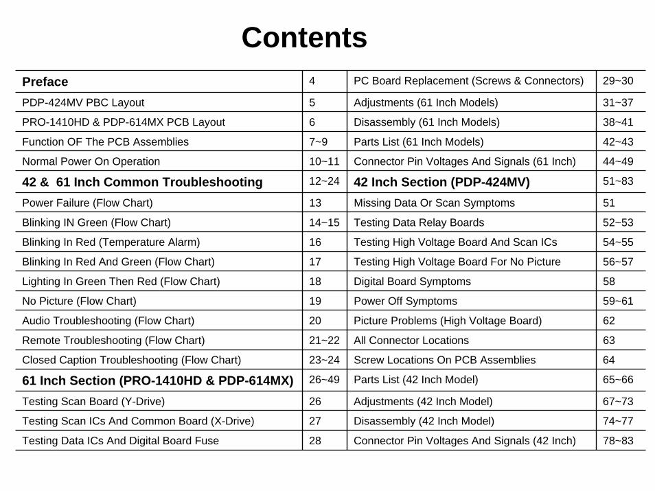
ContentsPreface 4 PC Board Replacement (Screws & Connectors) 29~30
PDP-424MV PBC Layout 5 Adjustments (61 Inch Models) 31~37
PRO-1410HD & PDP-614MX PCB Layout 6 Disassembly (61 Inch Models) 38~41
Function OF The PCB Assemblies 7~9 Parts List (61 Inch Models) 42~43
Normal Power On Operation 10~11 Connector Pin Voltages And Signals (61 Inch) 44~49
42 & 61 Inch Common Troubleshooting 12~24 42 Inch Section (PDP-424MV) 51~83
Power Failure (Flow Chart) 13 Missing Data Or Scan Symptoms 51
Blinking IN Green (Flow Chart) 14~15 Testing Data Relay Boards 52~53
Blinking In Red (Temperature Alarm) 16 Testing High Voltage Board And Scan ICs 54~55
Blinking In Red And Green (Flow Chart) 17 Testing High Voltage Board For No Picture 56~57
Lighting In Green Then Red (Flow Chart) 18 Digital Board Symptoms 58
No Picture (Flow Chart) 19 Power Off Symptoms 59~61
Audio Troubleshooting (Flow Chart) 20 Picture Problems (High Voltage Board) 62
Remote Troubleshooting (Flow Chart) 21~22 All Connector Locations 63
Closed Caption Troubleshooting (Flow Chart) 23~24 Screw Locations On PCB Assemblies 64
61 Inch Section (PRO-1410HD & PDP-614MX) 26~49 Parts List (42 Inch Model) 65~66
Testing Scan Board (Y-Drive) 26 Adjustments (42 Inch Model) 67~73
Testing Scan ICs And Common Board (X-Drive) 27 Disassembly (42 Inch Model) 74~77
Testing Data ICs And Digital Board Fuse 28 Connector Pin Voltages And Signals (42 Inch) 78~83
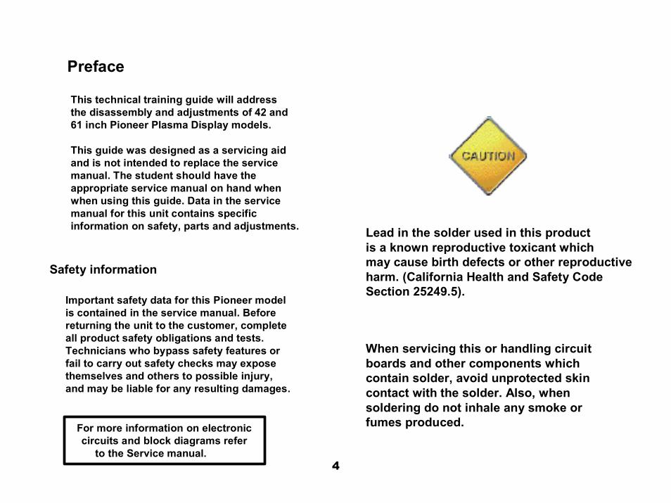
Lead in the solder used in this productis a known reproductive toxicant whichmay cause birth defects or other reproductiveharm. (California Health and Safety CodeSection 25249.5).
When servicing this or handling circuitboards and other components whichcontain solder, avoid unprotected skincontact with the solder. Also, when soldering do not inhale any smoke orfumes produced.
This technical training guide will addressthe disassembly and adjustments of 42 and 61 inch Pioneer Plasma Display models.
This guide was designed as a servicing aidand is not intended to replace the servicemanual. The student should have the appropriate service manual on hand whenwhen using this guide. Data in the servicemanual for this unit contains specificinformation on safety, parts and adjustments.
Safety information
Important safety data for this Pioneer modelis contained in the service manual. Before returning the unit to the customer, completeall product safety obligations and tests.Technicians who bypass safety features orfail to carry out safety checks may exposethemselves and others to possible injury,and may be liable for any resulting damages.
Preface
For more information on electroniccircuits and block diagrams refer
to the Service manual.4
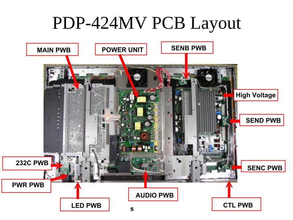
PDP-424MV PCB Layout POWER UNIT SENB PWB
SENC PWB
CTL PWB
232C PWB
LED PWB
PWR PWB
MAIN PWB
AUDIO PWB
SEND PWB
High Voltage
5
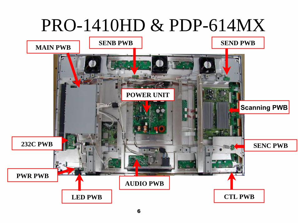
POWER UNIT
MAIN PWB
AUDIO PWB
PRO-1410HD & PDP-614MXSENB PWB SEND PWB
SENC PWB
CTL PWBLED PWB
PWR PWB
Scanning PWB
232C PWB
6
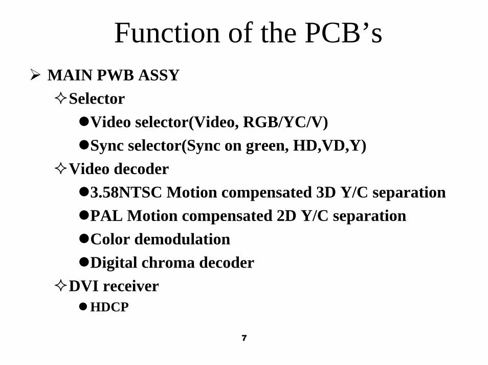
Function of the PCB’sMAIN PWB ASSY
SelectorVideo selector(Video, RGB/YC/V) Sync selector(Sync on green, HD,VD,Y)
Video decoder3.58NTSC Motion compensated 3D Y/C separation PAL Motion compensated 2D Y/C separation Color demodulationDigital chroma decoder
DVI receiverHDCP
7
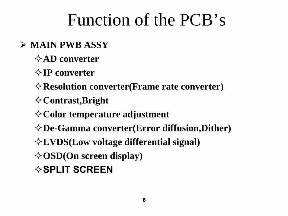
Function of the PCB’sMAIN PWB ASSY
AD converter IP converter Resolution converter(Frame rate converter) Contrast,BrightColor temperature adjustmentDe-Gamma converter(Error diffusion,Dither) LVDS(Low voltage differential signal) OSD(On screen display)SPLIT SCREEN
8
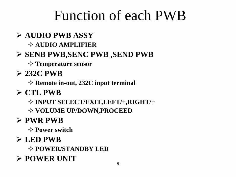
Function of each PWBAUDIO PWB ASSY
AUDIO AMPLIFIER SENB PWB,SENC PWB ,SEND PWB
Temperature sensor232C PWB
Remote in-out, 232C input terminalCTL PWB
INPUT SELECT/EXIT,LEFT/+,RIGHT/+VOLUME UP/DOWN,PROCEED
PWR PWBPower switch
LED PWBPOWER/STANDBY LED
POWER UNIT9
IC9503
CPU
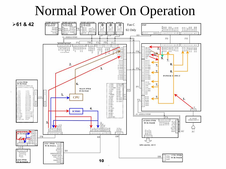
Normal Power On Operation61 & 42 Fan C
61 Only
1.
2.
2.
3.
4.
5.
6.
7.
7.
7.
7.
7.8.
8.3.
2.
9.
10
Normal Power On Operation
1. AC line attached to Power Supply. 2. Power Supply outputs a Power Mute voltage at +4.8 from Connector PM pin 5
(POMUTE). The Power Supply also outputs a +7 volt supply to the Main Microprocessor at Connector PM pin 1 (M+7).
3. The +7 volt supply now on the Main PCB goes to the RS232 PCB, Power Switch PCB and IC9503 the +5 volt regulator. Additionally the +7 volt supply returns back to the Power Supply as one of the Power Start Up signals.
4. The +5 volt regulator (IC9503) outputs to the RS232 and Power Switch PCB’s. At this time the Main Microprocessor sets the state to Standby and the front panel LED lights Red.
5. From Standby pressing the Power button will send a +5 volt signal to the Main Microprocessor from the Power Switch PCB Connector PW pin 2 (POIN).
6. The Main Microprocessor outputs the Power On +5 volt signal to the Power Supply from Connector PM pin 3 (POWER). At this time the Power Relay engages.
7. The Power Supply upon receiving the Power On Signal supplies all other secondary supply voltages.
8. After secondary supply voltages come up the power supplies for VS (170) and VD (65) turn on.
9. NOTE: Panel Alarm Input Line can shutdown the Power Supply (Low Normal).
11
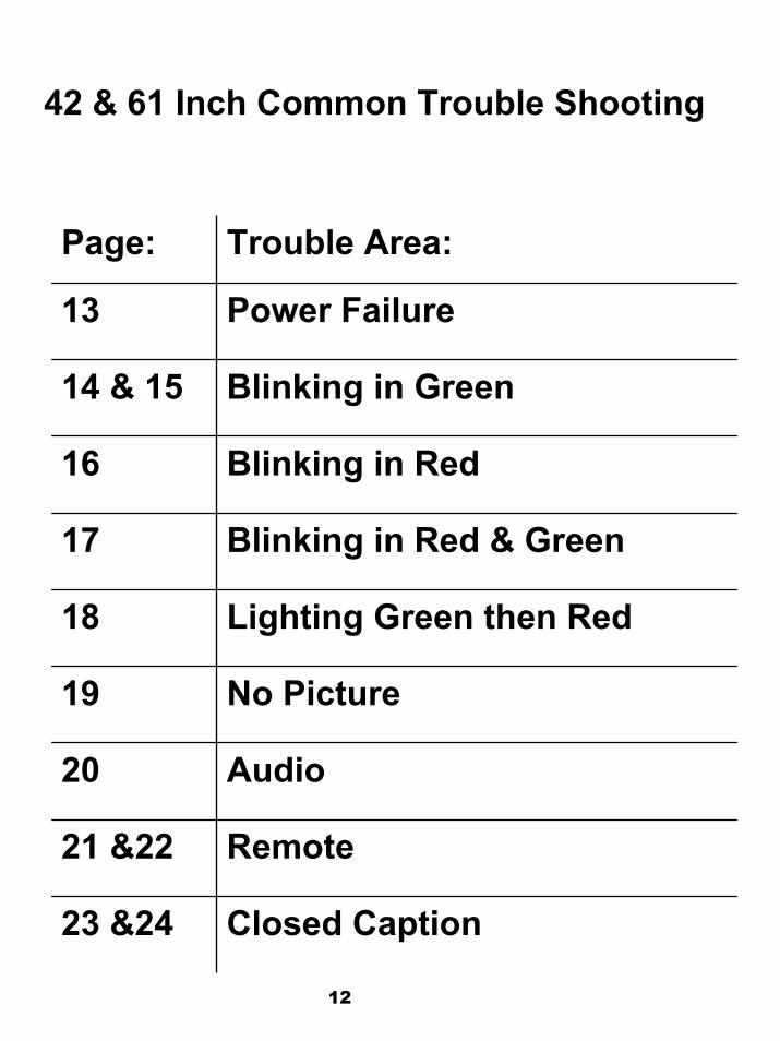
42 & 61 Inch Common Trouble Shooting
Page: Trouble Area:
13 Power Failure
14 & 15 Blinking in Green
16 Blinking in Red
17 Blinking in Red & Green
18 Lighting Green then Red
19 No Picture
20 Audio
21 &22 Remote
23 &24 Closed Caption
12
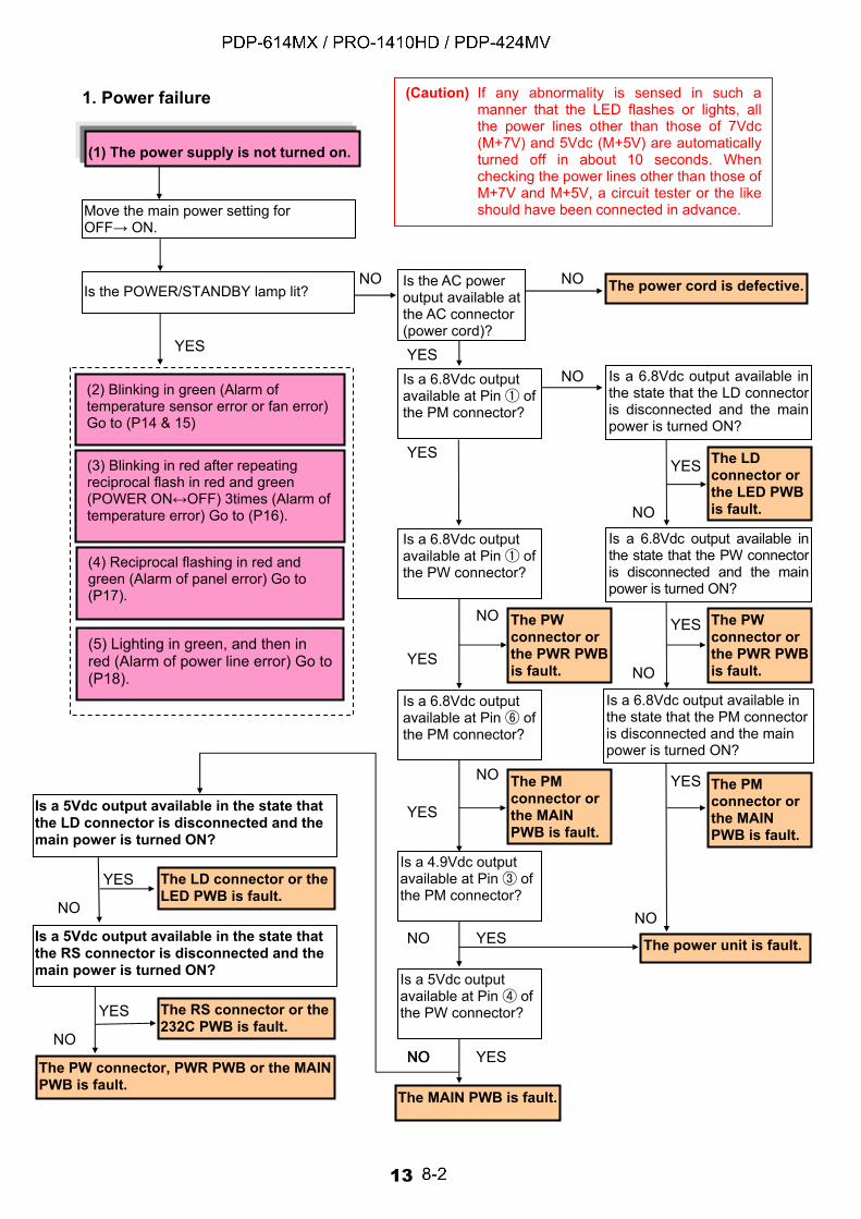
1. Power failure
YES
The power cord is defective.
The MAIN PWB is fault.
YES
Move the main power setting for OFF→ ON.
YES
(1) The power supply is not turned on.
The LD connector or the LED PWB is fault.
NO
The PW connector or the PWR PWB is fault.
The PM connector or the MAIN PWB is fault.
The power unit is fault.
The PW connector or the PWR PWB is fault.
The PM connector or the MAIN PWB is fault.
(Caution) If any abnormality is sensed in such a manner that the LED flashes or lights, all the power lines other than those of 7Vdc (M+7V) and 5Vdc (M+5V) are automatically turned off in about 10 seconds. When checking the power lines other than those of M+7V and M+5V, a circuit tester or the like should have been connected in advance.
(3) Blinking in red after repeating reciprocal flash in red and green (POWER ON↔OFF) 3times (Alarm of temperature error) Go to (P16).
(2) Blinking in green (Alarm of temperature sensor error or fan error) Go to (P14 & 15)
(4) Reciprocal flashing in red and green (Alarm of panel error) Go to (P17).
(5) Lighting in green, and then in red (Alarm of power line error) Go to (P18).
Is a 5Vdc output available in the state that the LD connector is disconnected and the main power is turned ON?
The LD connector or the LED PWB is fault.
YES
NO
Is a 5Vdc output available in the state that the RS connector is disconnected and the main power is turned ON?
The RS connector or the 232C PWB is fault.
YES
NO
The PW connector, PWR PWB or the MAIN PWB is fault.
Is a 6.8Vdc output available inthe state that the PW connectoris disconnected and the main power is turned ON?
Is a 6.8Vdc output available at Pin of the PM connector?
Is a 6.8Vdc output available inthe state that the LD connectoris disconnected and the main power is turned ON?
Is a 5Vdc output available at Pin of the PW connector?
Is a 4.9Vdc output available at Pin of the PM connector?
Is a 6.8Vdc output available at Pin of the PW connector?
Is a 6.8Vdc output available at Pin of the PM connector?
Is a 6.8Vdc output available in the state that the PM connector is disconnected and the main power is turned ON?
Is the AC power output available at the AC connector (power cord)?
Is the POWER/STANDBY lamp lit? NO
NO
YES
YES
YES
NO
NO NO NO
YES
YES
NO
NO
NO
NO
NO
YES
YES
13
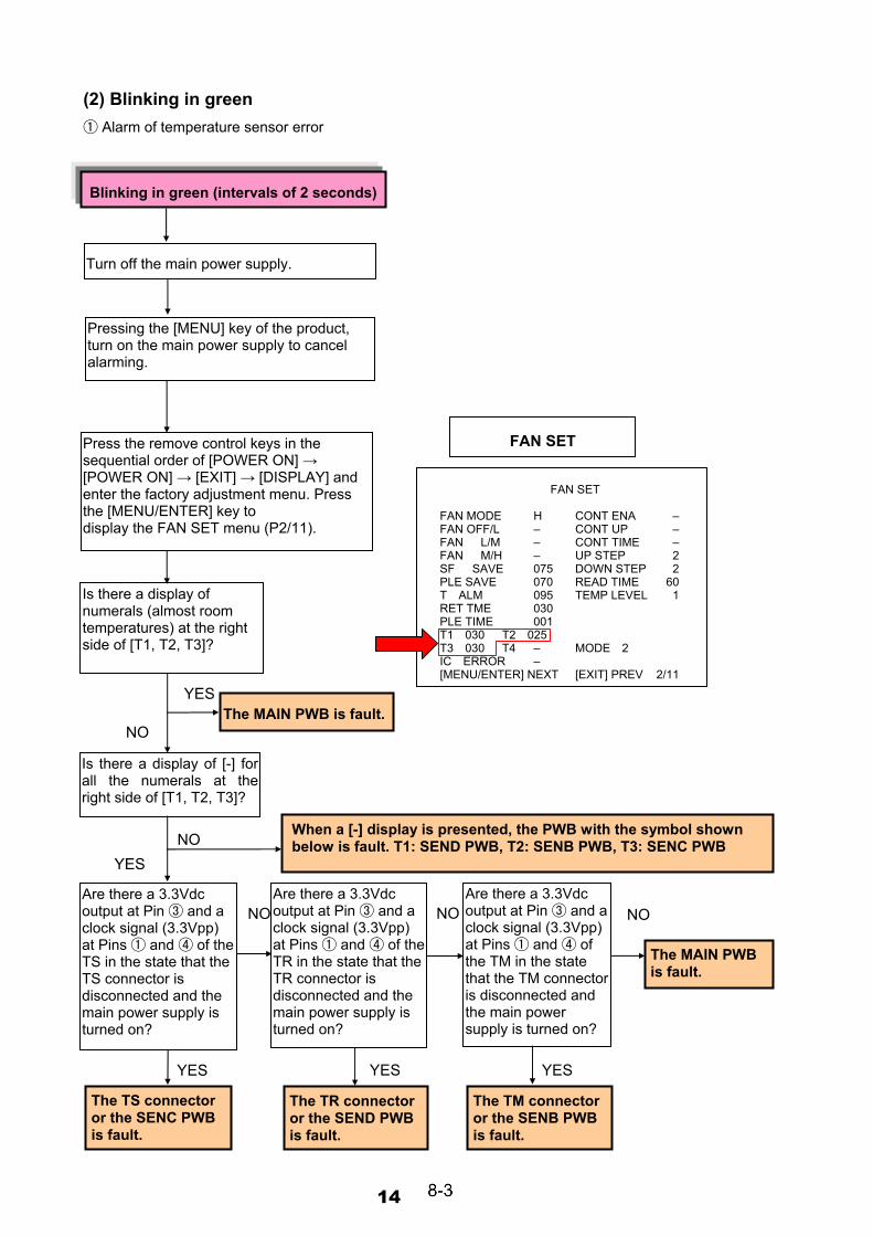
(2) Blinking in green Alarm of te mperature sensor error
YES
NO
The TS connector or the SENC PWB is fault.
NO
YES
The TR connector or the SEND PWB is fault.
Is there a display of numerals (almost room temperatures) at the right side of [T1, T2, T3]?
YES
NO When a [-] display is presented, the PWB with the symbol shown below is fault. T1: SEND PWB, T2: SENB PWB, T3: SENC PWB
Are there a 3.3Vdc output at Pin and a clock signal (3.3Vpp) at Pins and of the TR in the state that the TR connector is disconnected and the main power supply is turned on?
Are there a 3.3Vdc output at Pin and a clock signal (3.3Vpp) at Pins and of the TM in the state that the TM connector is disconnected and the main power supply is turned on?
YES
The TM connector or the SENB PWB is fault.
NO
The MAIN PWB is fault.
Is there a display of [-] for all the numerals at the right side of [T1, T2, T3]?
NO
YES
Press the remove control keys in the sequential order of [POWER ON] → [POWER ON] → [EXIT] → [DISPLAY] and enter the factory adjustment menu. Press the [MENU/ENTER] key to display the FAN SET menu (P2/11).
Blinking in green (intervals of 2 seconds)
FAN SET
Turn off the main power supply.
Pressing the [MENU] key of the product, turn on the main power supply to cancel alarming.
FAN SET
FAN MODE H CONT ENA – FAN OFF/L – CONT UP – FAN L/M – CONT TIME – FAN M/H – UP STEP 2 SF SAVE 075 DOWN STEP 2 PLE SAVE 070 READ TIME 60 T ALM 095 TEMP LEVEL 1 RET TME 030 PLE TIME 001 T1 030 T2 025 T3 030 T4 – MODE 2 IC ERROR – [MENU/ENTER] NEXT [EXIT] PREV 2/11
The MAIN PWB is fault.
Are there a 3.3Vdc output at Pin and a clock signal (3.3Vpp) at Pins and of the TS in the state that the TS connector is disconnected and the main power supply is turned on?
14
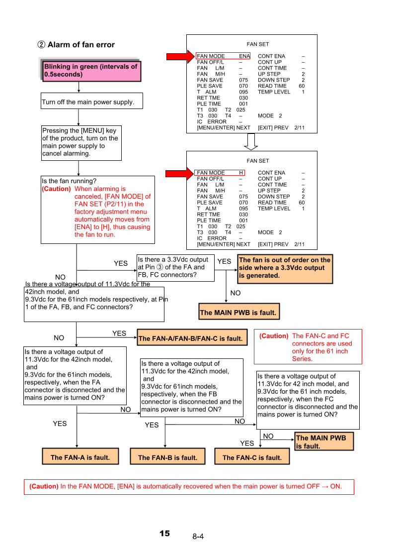
Alarm of fan error
FAN SET
FAN MODE H CONT ENA – FAN OFF/L – CONT UP – FAN L/M – CONT TIME – FAN M/H – UP STEP 2 FAN SAVE 075 DOWN STEP 2 PLE SAVE 070 READ TIME 60 T ALM 095 TEMP LEVEL 1 RET TME 030 PLE TIME 001 T1 030 T2 025 T3 030 T4 – MODE 2 IC ERROR – [MENU/ENTER] NEXT [EXIT] PREV 2/11
FAN SET
FAN MODE ENA CONT ENA – FAN OFF/L – CONT UP – FAN L/M – CONT TIME – FAN M/H – UP STEP 2 FAN SAVE 075 DOWN STEP 2 PLE SAVE 070 READ TIME 60 T ALM 095 TEMP LEVEL 1 RET TME 030 PLE TIME 001 T1 030 T2 025 T3 030 T4 – MODE 2 IC ERROR – [MENU/ENTER] NEXT [EXIT] PREV 2/11
NO
NO
YES YES
NO
The FAN-A is fault.
The MAIN PWB is fault.
Blinking in green (intervals of 0.5seconds)
NO
YES
YES
The FAN-B is fault.
The fan is out of order on the side where a 3.3Vdc output is generated.
YES
The FAN-A/FAN-B/FAN-C is fault.
NO
(Caution) In the FAN MODE, [ENA] is automatically recovered when the main power is turned OFF → ON.
The FAN-C is fault.
YESNO
(Caution) The FAN-C and FC connectors are used only for the 61 inchSeries.
The MAIN PWB is fault.
Is the fan running? (Caution) When alarming is
canceled, [FAN MODE] of FAN SET (P2/11) in the factory adjustment menu automatically moves from [ENA] to [H], thus causing the fan to run.
Is there a 3.3Vdc output at Pin of the FA and FB, FC connectors?
Is there a voltage output of 11.3Vdc for the 42inch model, and 9.3Vdc for the 61inch models, respectively, when the FA connector is disconnected and the mains power is turned ON?
Is there a voltage output of 11.3Vdc for the 42inch model, and 9.3Vdc for 61inch models, respectively, when the FB connector is disconnected and the mains power is turned ON?
Pressing the [MENU] key of the product, turn on the main power supply to cancel alarming.
Turn off the main power supply.
Is there a voltage output of 11.3Vdc for 42 inch model, and 9.3Vdc for the 61 inch models, respectively, when the FC connector is disconnected and the mains power is turned ON?
Is there a voltage output of 11.3Vdc for the42inch model, and 9.3Vdc for the 61inch models respectively, at Pin 1 of the FA, FB, and FC connectors?
15
(3) Blinking in red (Alarm of temperature error) Since the internal temperature is too high in the product, the temperature protector has been actuated. In such a case, the following actions should be taken immediately:
1. Turn off the main power supply and pull out the power cord from the wall outlet.
2. Wait for about 60 minutes until the temperature in the main unit lowers.
3. Check whether the heat discharge port is covered with dust or the like. If yes, remove the clogging substance.
4. If the unit is used where the ambient temperature is high, it should be moved to an adequate place (air temperature ranging from 5°C to 35°C).
16
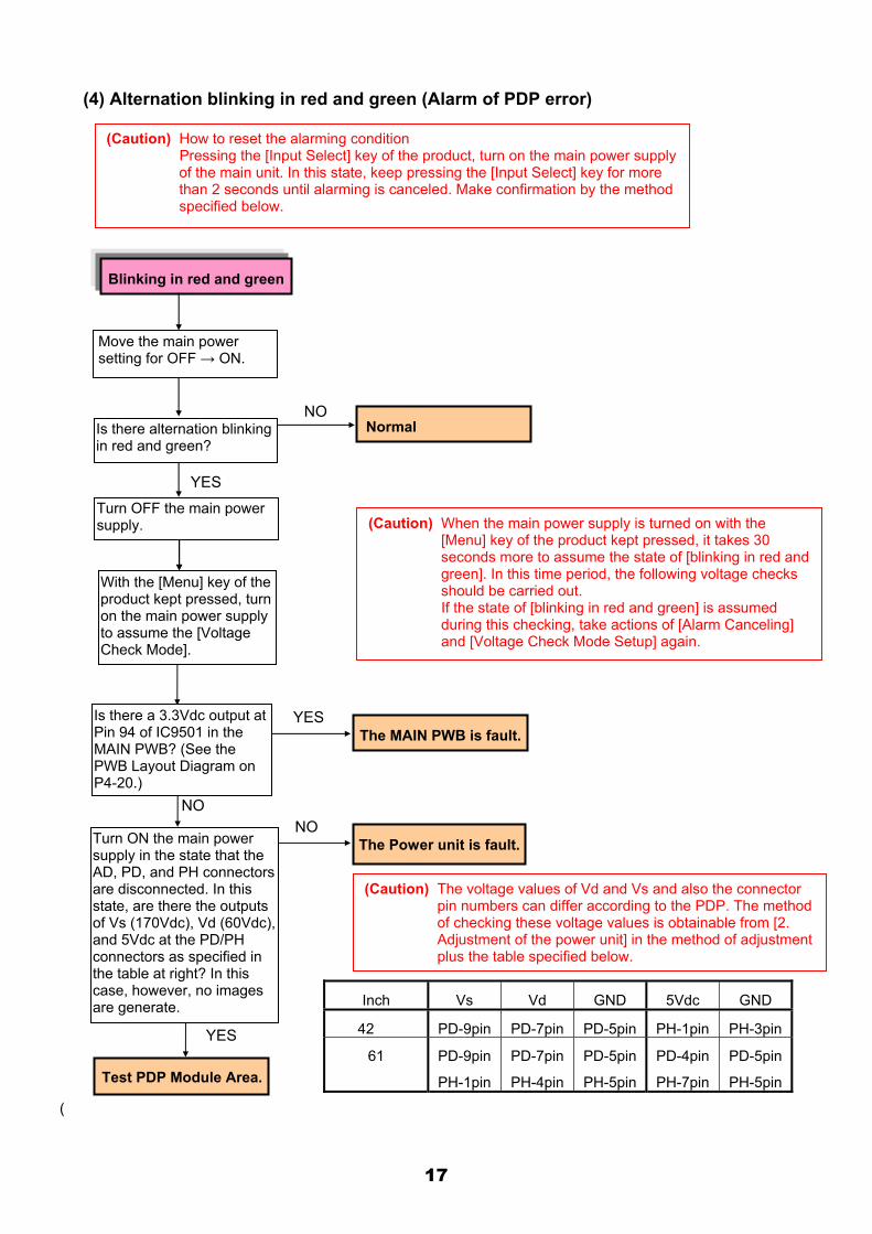
(4) Alternation blinking in red and green (Alarm of PDP error)
Inch Vs Vd GND 5Vdc GND
42 PD-9pin PD-7pin PD-5pin PH-1pin PH-3pin
61
PD-9pin
PH-1pin
PD-7pin
PH-4pin
PD-5pin
PH-5pin
PD-4pin
PH-7pin
PD-5pin
PH-5pin
YES
NO
The Power unit is fault.NO
Blinking in red and green
NO
YES
Normal
The MAIN PWB is fault.
(Caution) How to reset the alarming condition Pressing the [Input Select] key of the product, turn on the main power supply of the main unit. In this state, keep pressing the [Input Select] key for more than 2 seconds until alarming is canceled. Make confirmation by the method specified below.
(Caution) The voltage values of Vd and Vs and also the connector pin numbers can differ according to the PDP. The method of checking these voltage values is obtainable from [2. Adjustment of the power unit] in the method of adjustment plus the table specified below.
(Caution) When the main power supply is turned on with the [Menu] key of the product kept pressed, it takes 30 seconds more to assume the state of [blinking in red and green]. In this time period, the following voltage checks should be carried out. If the state of [blinking in red and green] is assumed during this checking, take actions of [Alarm Canceling] and [Voltage Check Mode Setup] again.
YES
Test PDP Module Area.
Is there a 3.3Vdc output at Pin 94 of IC9501 in the MAIN PWB? (See the PWB Layout Diagram on P4-20.)
Turn ON the main power supply in the state that the AD, PD, and PH connectors are disconnected. In this state, are there the outputs of Vs (170Vdc), Vd (60Vdc), and 5Vdc at the PD/PH connectors as specified in the table at right? In this case, however, no images are generate.
Move the main power setting for OFF → ON.
With the [Menu] key of the product kept pressed, turn on the main power supply to assume the [Voltage Check Mode].
(
Is there alternation blinking in red and green?
Turn OFF the main power supply.
17
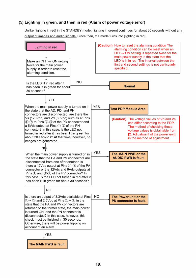
(5) Lighting in green, and then in red (Alarm of power voltage error)
Unlike [lighting in red] in the STANDBY mode, [lighting in green] continues for about 30 seconds without any
output of images and audio signals. Since then, the mode turns into [lighting in red].
YES
YES When the main power supply is turned on in the state that the AD, PD, and PH connectors are disconnected, are there the Vs (170Vdc) and Vd (60Vdc) outputs at Pins - to Pins - of the PD connector and a 5Vdc output at Pins - of the PH connector? In this case, is the LED not turned in red after it has been lit in green for about 30 seconds? At that time, however, no images are generated.
Test PDP Module Area.
NO
NO
NO
(Caution) How to reset the alarming condition The alarming condition can be reset when an OFF→ ON setting is repeated twice for the main power supply in the state that the LED is lit in red. The interval between the first and second settings is not particularly specified.
Lighting in red
Normal NO
YES
The MAIN PWB or the AUDIO PWB is fault.
The Power unit or the PN connector is fault.
(Caution) The voltage values of Vd and Vs can differ according to the PDP. The method of checking these voltage values is obtainable from [2. Adjustment of the power unit] in the method of adjustment.
YES
The MAIN PWB is fault.
Make an OFF → ON setting twice for the main power supply in order to reset the alarming condition.
Is the LED lit in red after it has been lit in green for about 30 seconds?
When the main power supply is turned on in the state that the PA and PV connectors are disconnected from one after another, is there a 12Vdc output at Pins - of the PA connector or the 12Vdc and 6Vdc outputs at Pins and - of the PV connector? In this case, is the LED not turned in red after it has been lit in green for about 30 seconds?
Is there an output of 3.3Vdc available at Pins ~ and 2.5Vdc at Pins ~ in the
state that the PA and PV connectors are returned to the former state, the main power is turned ON, and the PN connector is disconnected? In this case, however, this check must be finished in 30 seconds. Otherwise, there will be power tripping on account of an alarm.
18
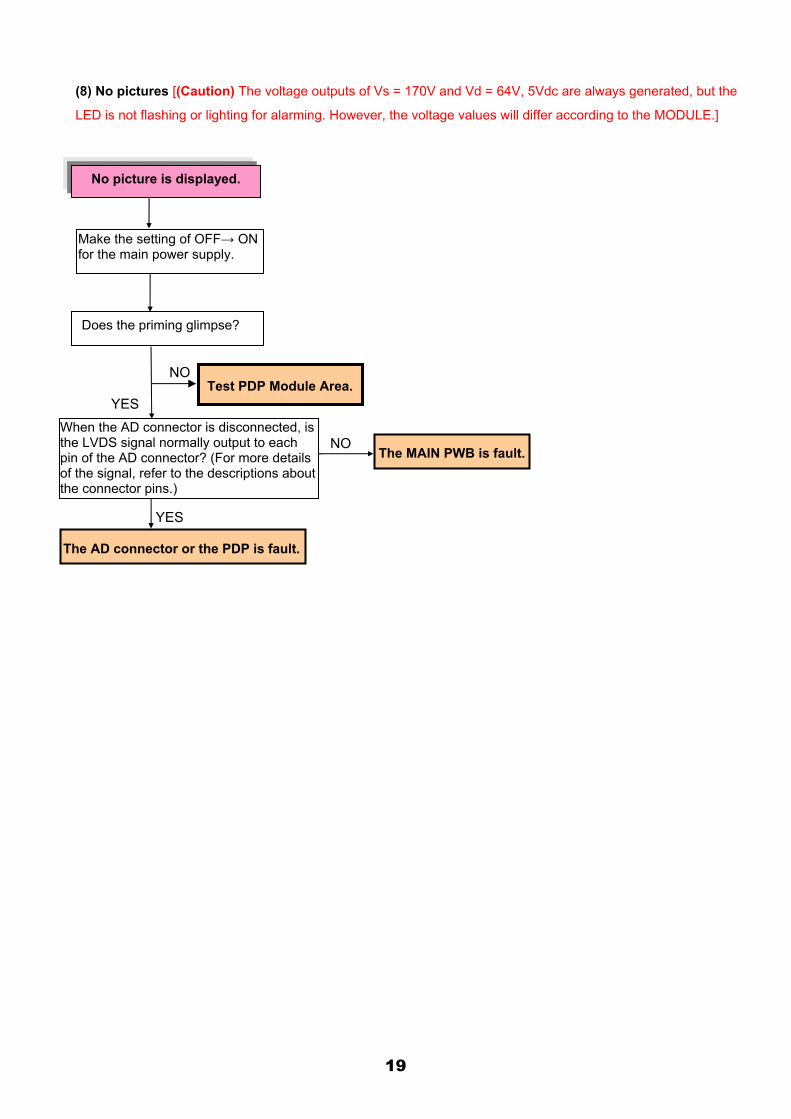
(8) No pictures [(Caution) The voltage outputs of Vs = 170V and Vd = 64V, 5Vdc are always generated, but the
LED is not flashing or lighting for alarming. However, the voltage values will differ according to the MODULE.]
YES
YES
NO
The AD connector or the PDP is fault.
The MAIN PWB is fault.
No picture is displayed.
Does the priming glimpse?
NO Test PDP Module Area.
Make the setting of OFF→ ON for the main power supply.
When the AD connector is disconnected, is the LVDS signal normally output to each pin of the AD connector? (For more details of the signal, refer to the descriptions about the connector pins.)
19
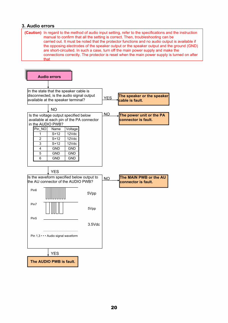
3. Audio errors
YES
Is the voltage output specified below available at each pin of the PA connector in the AUDIO PWB?
Pin_NO Name Voltage 1 S+12 12Vdc 2 S+12 12Vdc 3 S+12 12Vdc 4 GND GND 5 GND GND 6 GND GND
The power unit or the PA connector is fault.
NO NO
YES
Is the waveform specified below output to the AU connector of the AUDIO PWB?
Pin6
Pin7
Pin5
Pin 1,3 • • • Audio signal waveform
NO
The AUDIO PWB is fault.
YES
The speaker or the speaker cable is fault.
In the state that the speaker cable is disconnected, is the audio signal output available at the speaker terminal?
5Vpp
5Vpp
3.5Vdc
The MAIN PWB or the AU connector is fault.
(Caution) In regard to the method of audio input setting, refer to the specifications and the instruction manual to confirm that all the setting is correct. Then, troubleshooting can be carried out. It must be noted that the protector functions and no audio output is available if the opposing electrodes of the speaker output or the speaker output and the ground (GND) are short-circuited. In such a case, turn off the main power supply and make the connections correctly. The protector is reset when the main power supply is turned on after that
Audio errors
20
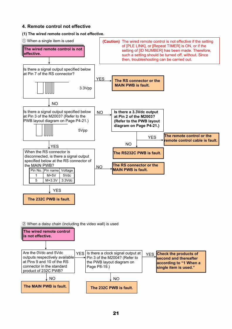
4. Remote control not effective (1) The wired remote control is not effective.
When a single item is used
When a daisy chain (including the video wall) is used
Is there a signal output specified below at Pin 7 of the RS connector?
3.3Vpp
YES
The RS232C PWB is fault.
NO
Is there a signal output specified below at Pin 3 of the M2003? (Refer to the PWB layout diagram on Page P4-21.) 5Vpp
YES
NO
When the RS connector is disconnected, is there a signal output specified below at the RS connector of the MAIN PWB?
Pin No. Pin name Voltage 1 M+5V 5Vdc5 M+3.3V 3.3Vdc
NO
YES
Is there a 3.3Vdc output at Pin 2 of the M2003? (Refer to the PWB layout diagram on Page P4-21.)
The remote control or the remote control cable is fault.
YES
The RS connector or the MAIN PWB is fault.
The 232C PWB is fault.
The 232C PWB is fault.
Are the 0Vdc and 5Vdc outputs respectively available at Pins 9 and 10 of the RS connector in the standard product of 232C PWB?
NO
The MAIN PWB is fault.
YES
The wired remote control is not effective.
(Caution) The wired remote control is not effective if the setting of [PLE LINK], or [Repeat TIMER] is ON, or if the setting of [ID NUMBER] has been made. Therefore, such a setting should be turned off, without. Since then, troubleshooting can be carried out.
NO
Check the products of second and thereafter according to “1 When a single item is used.”
YES
The RS connector or the MAIN PWB is fault.
NO
The wired remote control is not effective.
Is there a clock signal output at Pin 3 of the M2004? (Refer to the PWB layout diagram on Page P8-19.)
21
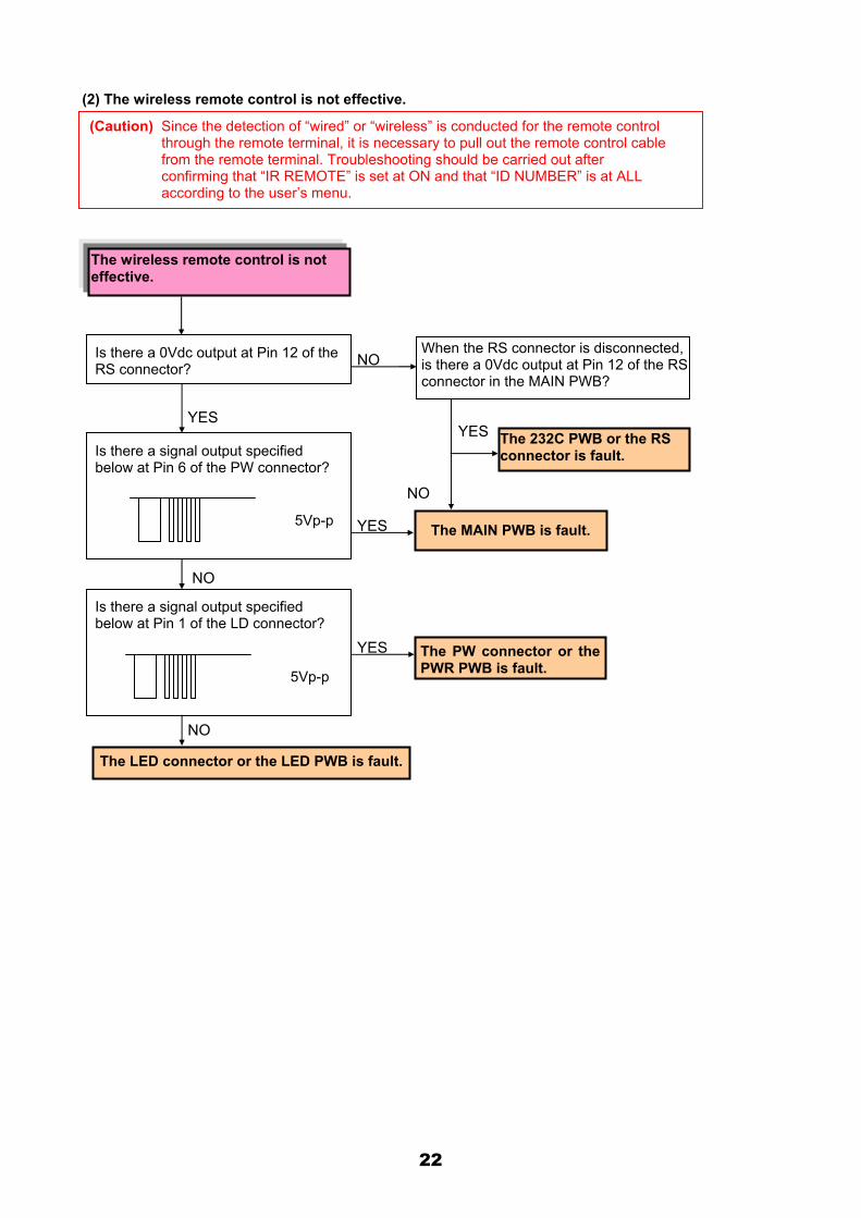
(2) The wireless remote control is not effective.
Is there a signal output specified below at Pin 6 of the PW connector?
5Vp-p YES
NO
Is there a signal output specified below at Pin 1 of the LD connector?
5Vp-p
NO
YES
NO
The 232C PWB or the RS connector is fault.
YES
Is there a 0Vdc output at Pin 12 of the RS connector?
YES
NO
(Caution) Since the detection of “wired” or “wireless” is conducted for the remote control through the remote terminal, it is necessary to pull out the remote control cable from the remote terminal. Troubleshooting should be carried out after confirming that “IR REMOTE” is set at ON and that “ID NUMBER” is at ALL according to the user’s menu.
The wireless remote control is not effective.
The LED connector or the LED PWB is fault.
The PW connector or the PWR PWB is fault.
The MAIN PWB is fault.
When the RS connector is disconnected, is there a 0Vdc output at Pin 12 of the RS connector in the MAIN PWB?
22
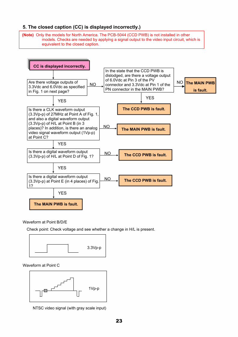
5. The closed caption (CC) is displayed incorrectly.)
Waveform at Point B/D/E
Check point: Check voltage and see whether a change in H/L is present.
Waveform at Point C
CC is displayed incorrectly.
(Note) Only the models for North America. The PCB-5044 (CCD PWB) is not installed in other models. Checks are needed by applying a signal output to the video input circuit, which is equivalent to the closed caption.
The MAIN PWB
is fault.
The CCD PWB is fault.
NO
Is there a digital waveform output (3.3Vp-p) of H/L at Point D of Fig. 1?
NO
YES
NO
YES
The CCD PWB is fault.
The MAIN PWB is fault.
YES
YES
The MAIN PWB is fault. NO
3.3Vp-p
NTSC video signal (with gray scale input)
1Vp-p
In the state that the CCD PWB is dislodged, are there a voltage output of 6.0Vdc at Pin 3 of the PV connector and 3.3Vdc at Pin 1 of the PN connector in the MAIN PWB?
NO
YES
The CCD PWB is fault.
Is there a digital waveform output (3.3Vp-p) at Point E (in 4 places) of Fig. 1?
Is there a CLK waveform output (3.3Vp-p) of 27MHz at Point A of Fig. 1, and also a digital waveform output (3.3Vp-p) of H/L at Point B (in 3 places)? In addition, is there an analog video signal waveform output (1Vp-p) at Point C?
Are there voltage outputs of 3.3Vdc and 6.0Vdc as specified in Fig. 1 on next page?
23
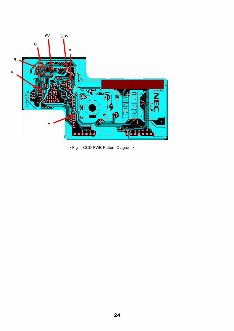
<Fig. 1 CCD PWB Pattern Diagram>
A
B
D
E
3.3V 6V
C
24
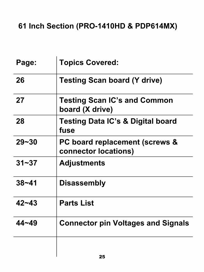
61 Inch Section (PRO-1410HD & PDP614MX)
Page: Topics Covered:
26 Testing Scan board (Y drive)
27 Testing Scan IC’s and Common board (X drive)
28 Testing Data IC’s & Digital board fuse
29~30 PC board replacement (screws & connector locations)
31~37 Adjustments
38~41 Disassembly
42~43 Parts List
44~49 Connector pin Voltages and Signals
25
1
8
11
273031
OK: Short-circuited,
NG: Open
OK: Short-circuited,
NG: Open
OK: Short-circuited,
NG: Open
OK: Short-circuited,
NG: Open
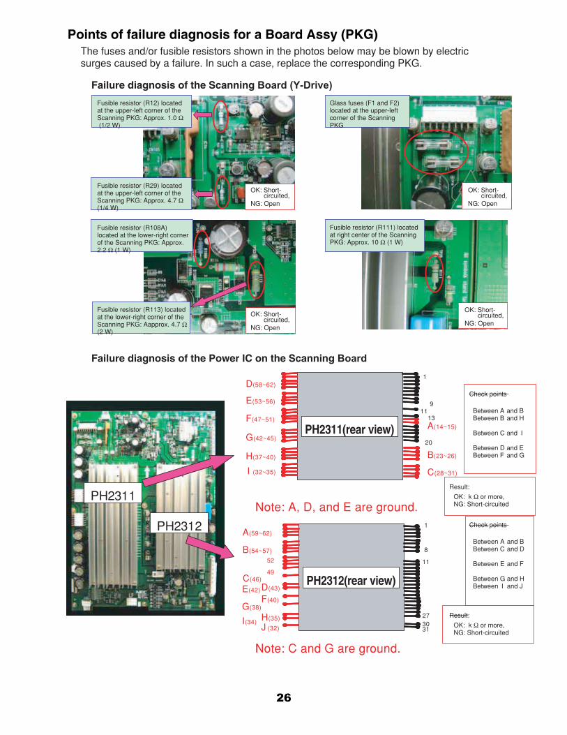
Points of failure diagnosis for a Board Assy (PKG)The fuses and/or fusible resistors shown in the photos below may be blown by electric surges caused by a failure. In such a case, replace the corresponding PKG.
Failure diagnosis of the Scanning Board (Y-Drive)
Failure diagnosis of the Power IC on the Scanning Board
Fusible resistor (R12) located at the upper-left corner of the Scanning PKG: Approx. 1.0 Ω (1/2 W)
Glass fuses (F1 and F2) located at the upper-left corner of the Scanning PKG
Fusible resistor (R111) located at right center of the Scanning PKG: Approx. 10 Ω (1 W)
Fusible resistor (R29) located at the upper-left corner of the Scanning PKG: Approx. 4.7 Ω (1/4 W)
Fusible resistor (R108A) located at the lower-right corner of the Scanning PKG: Approx. 2.2 Ω (1 W)
Fusible resistor (R113) located at the lower-right corner of the Scanning PKG: Aapprox. 4.7 Ω (2 W)
PH2311(rear view)
PH2312(rear view)
1
A(14~15)
D(58~62)
A(59~62)
B(54~57)
C(46)
E(42)
G(38)
I(34)
D(43)
F(40)
H(35)
J (32)
52
49
E(53~56)
F(47~51)
G(42~45)
H(37~40)
I (32~35)
B(23~26)
C(28~31)
1113
9
20
Note: A, D, and E are ground.
Note: C and G are ground.
PH2311
PH2312
Check points
Result:
Check points
Between A and B Between B and H Between C and I
Between D and E Between F and G
Between A and B Between C and D
Between E and F
Between G and H Between I and J
OK: k Ω or more, NG: Short-circuited
Result:
OK: k Ω or more, NG: Short-circuited
26
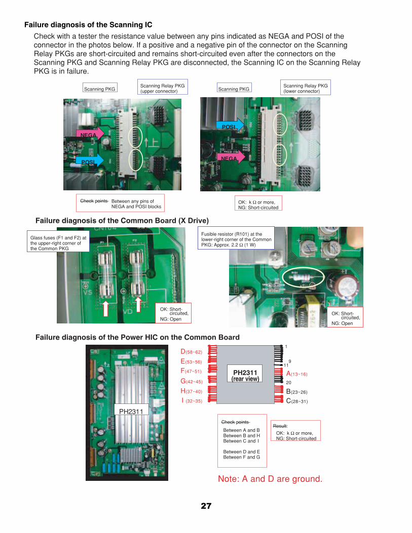
Failure diagnosis of the Power HIC on the Common Board1
119
20
OK: Short-circuited,
NG: Open OK: Short-
circuited, NG: Open
Failure diagnosis of the Scanning IC
Check with a tester the resistance value between any pins indicated as NEGA and POSI of the connector in the photos below. If a positive and a negative pin of the connector on the Scanning Relay PKGs are short-circuited and remains short-circuited even after the connectors on the Scanning PKG and Scanning Relay PKG are disconnected, the Scanning IC on the Scanning Relay PKG is in failure.
Failure diagnosis of the Common Board (X Drive)
Glass fuses (F1 and F2) at the upper-right corner of the Common PKG
Fusible resistor (R101) at the lower-right corner of the Common PKG: Approx. 2.2 Ω (1 W)
A(13~16)
B(23~26)
C(28~31)
D(58~62)
E(53~56)
F(47~51)
G(42~45)
H(37~40)
I (32~35)
Check points
Check points
Between A and B Between B and H Between C and I
Between D and E Between F and G
OK: k Ω or more, NG: Short-circuited
Between any pins of NEGA and POSI blocks
PH2311
NEGANEGA
POSIPOSINEGANEGA
POSIPOSI
Scanning Relay PKG (upper connector)Scanning PKG Scanning PKG
Scanning Relay PKG (lower connector)
PH2311(rear view)
Result:
OK: k Ω or more, NG: Short-circuited
Note: A and D are ground.
27
OK: OpenNG: Short- circuited,
OK: Short- circuited, NG: Open
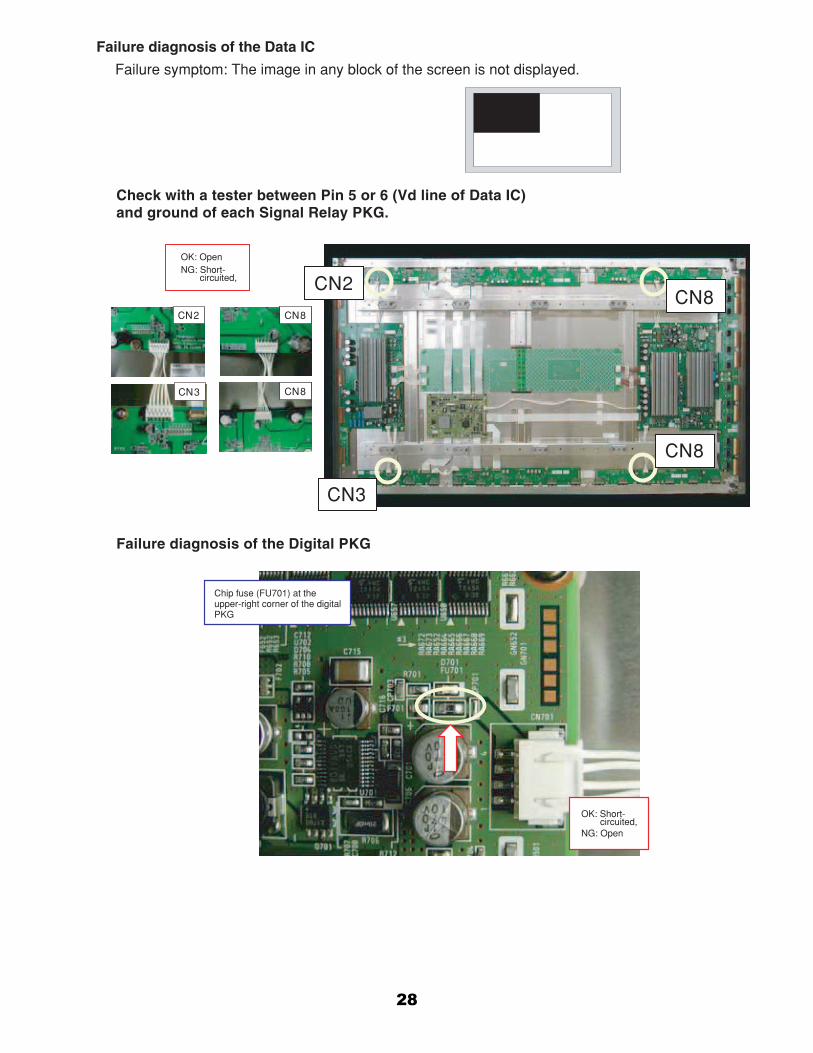
Failure diagnosis of the Data IC
Failure symptom: The image in any block of the screen is not displayed.
Chip fuse (FU701) at the upper-right corner of the digital PKG
CN2
CN3
CN8
CN8
CN8
CN8CN8CN2
CN3
Check with a tester between Pin 5 or 6 (Vd line of Data IC) and ground of each Signal Relay PKG.
Failure diagnosis of the Digital PKG
28
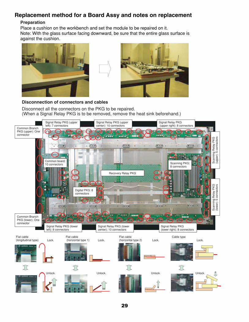
Replacement method for a Board Assy and notes on replacementPreparationPlace a cushion on the workbench and set the module to be repaired on it.Note: With the glass surface facing downward, be sure that the entire glass surface is against the cushion.
Common Branch PKG (upper): One connector
Common board: 10 connectors
Flat cable (longitudinal type)
Flat cable (horizontal type 1)
Flat cable (horizontal type 2)
Cable type
Digital PKG: 8 connectors
Scanning PKG: 8 connectors
Common Branch PKG (lower): One connector
Signal Relay PKG (upper left): 7 connectors
Signal Relay PKG (upper center): 10 connectors
Signal Relay PKG (upper right): 8 connectors
Signal Relay PKG (lower right): 8 connectors
Signal Relay PKG (lower center): 10 connectors
Signal Relay PKG (lower left): 8 connectors
Sca
nnin
g R
elay
PK
G
(upp
er):
5 c
onne
ctor
sS
cann
ing
Rel
ay P
KG
(lo
wer
): 5
con
nect
ors
Disconnection of connectors and cables
Disconnect all the connectors on the PKG to be repaired. (When a Signal Relay PKG is to be removed, remove the heat sink beforehand.)
Recovery Relay PKG
Lock. Lock. Lock. Lock.
Unlock. Unlock. Unlock. Unlock.
29
Scanning PKG: 9 screws
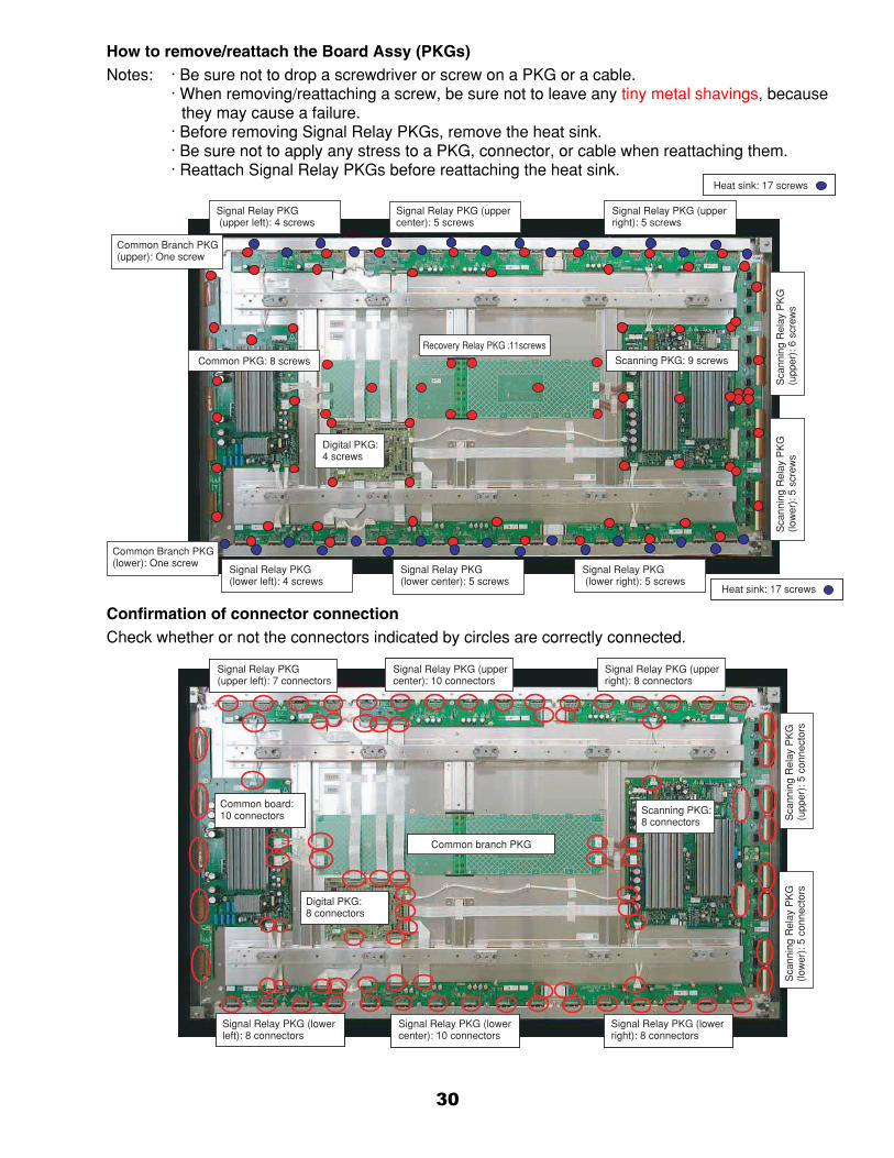
How to remove/reattach the Board Assy (PKGs)Notes: · Be sure not to drop a screwdriver or screw on a PKG or a cable.
· When removing/reattaching a screw, be sure not to leave any tiny metal shavings, because they may cause a failure.
· Before removing Signal Relay PKGs, remove the heat sink.· Be sure not to apply any stress to a PKG, connector, or cable when reattaching them.· Reattach Signal Relay PKGs before reattaching the heat sink.
Confirmation of connector connectionCheck whether or not the connectors indicated by circles are correctly connected.
Common Branch PKG (upper): One screw
Digital PKG: 4 screws
Common Branch PKG (lower): One screw
Signal Relay PKG (upper left): 4 screws
Signal Relay PKG (upper center): 5 screws
Signal Relay PKG (upper right): 5 screws
Signal Relay PKG (lower right): 5 screws
Signal Relay PKG (lower center): 5 screws
Signal Relay PKG (lower left): 4 screws
Signal Relay PKG (upper left): 7 connectors
Common board: 10 connectors Scanning PKG:
8 connectors
Signal Relay PKG (upper center): 10 connectors
Signal Relay PKG (upper right): 8 connectors
Signal Relay PKG (lower right): 8 connectors
Signal Relay PKG (lower center): 10 connectors
Signal Relay PKG (lower left): 8 connectors
Sca
nnin
g R
elay
PK
G
(upp
er):
5 c
onne
ctor
sS
cann
ing
Rel
ay P
KG
(lo
wer
): 5
con
nect
ors
Sca
nnin
g R
elay
PK
G
(upp
er):
6 s
crew
sS
cann
ing
Rel
ay P
KG
(lo
wer
): 5
scr
ews
Heat sink: 17 screws
Heat sink: 17 screws
Common PKG: 8 screws
Recovery Relay PKG :11screws
Digital PKG: 8 connectors
Common branch PKG
30
Adjusting conditions Adjustments should be carried out in the procedures of A to C specified below. However, any adjustments other than the items A to C below are not required.
A. When the “PDP module (PDP-NP61C2MF01)” is replaced, adjustmentsshould conform to the adjusting items of [1 and 2] specified below.
B. When the “POWER UNIT” is replaced, adjustments should conform to the adjusting item of [2] specified below.
C. When the “MAIN PWB” is replaced, adjustments should conform to the adjusting item of [3] specified below.
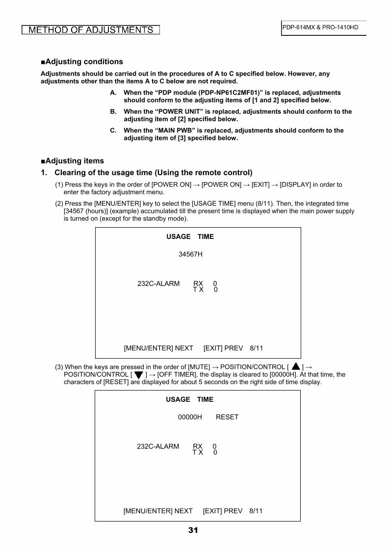
Adjusting items 1. Clearing of the usage time (Using the remote control)
(1) Press the keys in the order of [POWER ON] → [POWER ON] → [EXIT] → [DISPLAY] in order to enter the factory adjustment menu.
(2) Press the [MENU/ENTER] key to select the [USAGE TIME] menu (8/11). Then, the integrated time [34567 (hours)] (example) accumulated till the present time is displayed when the main power supply is turned on (except for the standby mode).
(3) When the keys are pressed in the order of [MUTE] → POSITION/CONTROL [ ] →
POSITION/CONTROL [ ] → [OFF TIMER], the display is cleared to [00000H]. At that time, the characters of [RESET] are displayed for about 5 seconds on the right side of time display.
USAGE TIME 34567H 232C-ALARM RX 0
T X 0
[MENU/ENTER] NEXT [EXIT] PREV 8/11
USAGE TIME 00000H RESET 232C-ALARM RX 0
T X 0
[MENU/ENTER] NEXT [EXIT] PREV 8/11
31
2-1. Adjustment of the Vs voltage
(1) Enter a color bar input by means of either video signal of VIDEO input, or DVD/HD input, or RGB input, and turn on the power switch of the main unit.
(2) Turn the volume control (RV6) in the power unit and make adjustments until the voltages of CH2 and CH1 (D, GND) of the power unit attain the voltage values specified for the PDP (Vs value of the voltage regulation indicator label on below the figure) ±1V.
2-2. Adjustment of the Vd voltage
(1) Enter a color bar input by means of either video signal of VIDEO input, or DVD/HD input, or RGB input, and turn on the power switch of the main unit.
(2) Confirm that the voltages of CH4 and CH1 (D, GND) of the power unit are maintained at the voltage values specified for the PDP (Vd value of the voltage regulation indicator label on below the figure) ±1V. Otherwise, turn the volume control (RV5) until the voltage attains the voltage values specified for the PDP (Vd value of the voltage regulation indicator label on below the figure) ±1V.
2-3. Adjustment of the +5V voltage
(1) Display a color bar by means of either video signal of VIDEO input, or DVD/HD input, or RGB input.
(2) Confirm that the voltages of CH3 and CH1 (D, GND) of the power unit are maintained at “5.15 ± 0.1V”. Otherwise, turn the volume control (RV2) until the voltage attains “5.15 ± 0.1V”.
(Caution) Rear-side view when the back cover is removed The label is concealed between the MAIN PWB and PDP. Check it by peeping through the space from above. The label position can be changed, without notice.
SERIAL NO. ******** Vd= **V Vs=***V CODE -01
Vs/Vd/100/185/220 V
555/84.2/782/10204 K
347 W/0 /2 P
OR
2. Adjustment of the power unit (Using a screwdriver for general-purposeadjustments)
32
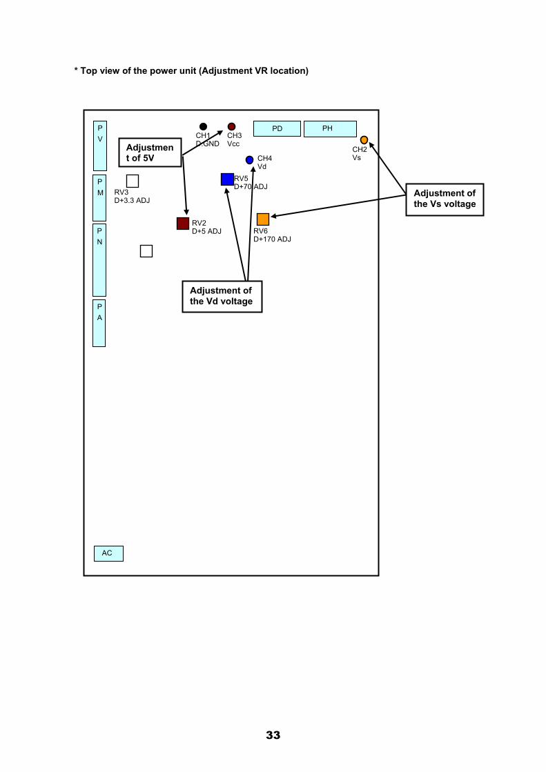
* Top view of the power unit (Adjustment VR location)
PH PD
PA
PN
PM
PV
AC
CH3Vcc
CH4 Vd
CH2Vs
RV5 D+70 ADJ
RV6 D+170 ADJ
CH1 D.GND
RV2 D+5 ADJ
RV3 D+3.3 ADJ
Adjustment of 5V
Adjustment of the Vd voltage
Adjustment of the Vs voltage
33
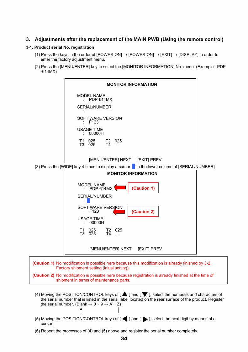
3. Adjustments after the replacement of the MAIN PWB (Using the remote control) 3-1. Product serial No. registration
(1) Press the keys in the order of [POWER ON] → [POWER ON] → [EXIT] → [DISPLAY] in order to enter the factory adjustment menu.
(2) Press the [MENU/ENTER] key to select the [MONITOR INFORMATION] No. menu. (Example : PDP-614MX)
(3) Press the [WIDE] key 4 times to display a cursor in the lower column of [SERIAL/NUMBER].
(4) Moving the POSITION/CONTROL keys of [ ] and [ ], select the numerals and characters of
the serial number that is listed in the serial label located on the rear surface of the product. Register the serial number. (Blank → 0 ~ 9 → A ~ Z)
(5) Moving the POSITION/CONTROL keys of [ ] and [ ], select the next digit by means of a cursor.
(6) Repeat the processes of (4) and (5) above and register the serial number completely.
(Caution 1) No modification is possible here because this modification is already finished by 3-2. Factory shipment setting (initial setting).
(Caution 2) No modification is possible here because registration is already finished at the time of shipment in terms of maintenance parts.
MONITOR INFORMATION
MODEL NAME : PDP-614MX
SERIAL/NUMBER : SOFT WARE VERSION : F123 USAGE TIME : 00000H T1 025 T2 025
T3 025 T4 - - [MENU/ENTER] NEXT [EXIT] PREV
MONITOR INFORMATION
MODEL NAME : PDP-614MX
SERIAL/NUMBER : SOFT WARE VERSION : F123 USAGE TIME : 00000H T1 025 T2 025
T3 025 T4 - - [MENU/ENTER] NEXT [EXIT] PREV
(Caution 1)
(Caution 2)
34
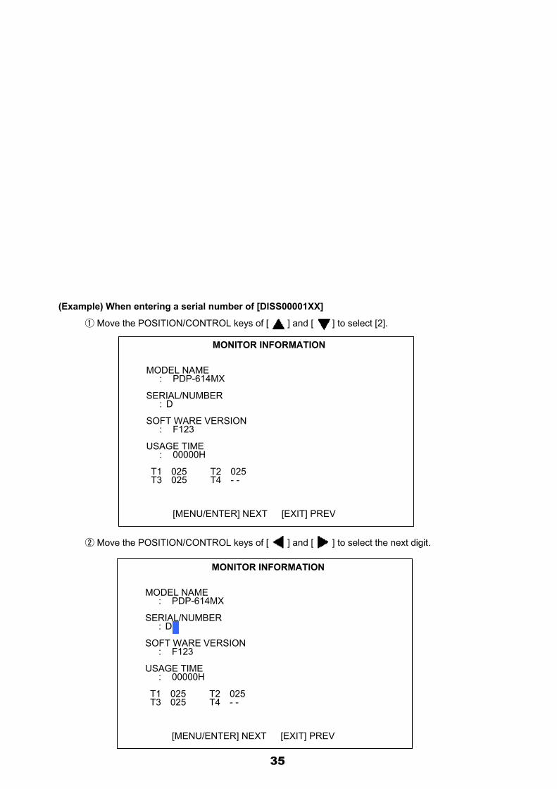
(Example) When entering a serial number of [DISS00001XX]
Move the POSITION/CONTROL keys of [ ] and [ ] to select [2].
Move the POSITION/CONTROL keys of [ ] and [ ] to select the next digit.
MONITOR INFORMATION
MODEL NAME : PDP-614MX
SERIAL/NUMBER : D SOFT WARE VERSION : F123 USAGE TIME : 00000H T1 025 T2 025
T3 025 T4 - - [MENU/ENTER] NEXT [EXIT] PREV
MONITOR INFORMATION
MODEL NAME : PDP-614MX
SERIAL/NUMBER : D SOFT WARE VERSION : F123 USAGE TIME : 00000H T1 025 T2 025
T3 025 T4 - - [MENU/ENTER] NEXT [EXIT] PREV
35
Repeat the procedures of and above, and enter all inputs of [DISS00001XX] from the left side.
(7) Following the above, setting must be carried out without fail according to “3-2. Factory shipment setting (Initial setting)”
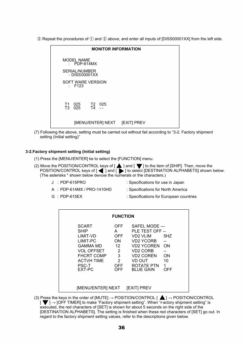
3-2.Factory shipment setting (Initial setting)
(1) Press the [MENU/ENTER] ke to select the [FUNCTION] menu.
(2) Move the POSITION/CONTROL keys of [ ] and [ ] to the item of [SHIP]. Then, move the POSITION/CONTROL keys of [ ] and [ ] to select [DESTINATION ALPHABETS] shown below. (The asterisks * shown below denote the numerals or the characters.)
J : PDP-615PRO : Specifications for use in Japan
A : PDP-614MX / PRO-1410HD : Specifications for North America
G : PDP-615EX : Specifications for European countries
(3) Press the keys in the order of [MUTE] → POSITION/CONTROL [ ] → POSITION/CONTROL
[ ] → [OFF TIMER] to make “Factory shipment setting”. When “Factory shipment setting” is executed, the red characters of [SET] is shown for about 5 seconds on the right side of the [DESTINATION ALPHABETS]. The setting is finished when these red characters of [SET] go out. In regard to the factory shipment setting values, refer to the descriptions given below.
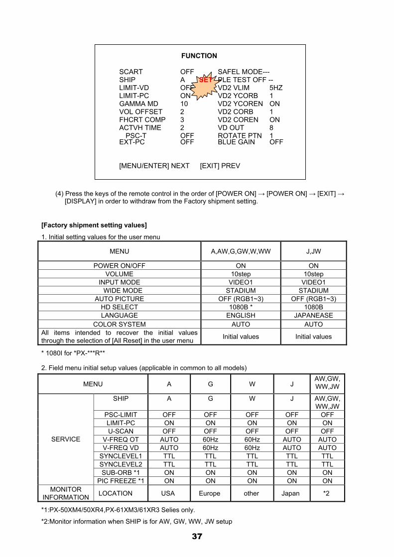
FUNCTION
SCART OFF SAFEL MODE --- SHIP A PLE TEST OFF -- LIMIT-VD OFF VD2 VLIM 5HZ LIMIT-PC ON VD2 YCORB -- GAMMA MD 12 VD2 YCOREN ON VOL OFFSET 2 VD2 CORB -- FHCRT COMP 3 VD2 COREN ON ACTVH TIME 2 VD OUT 10 PSC-T OFF ROTATE PTN 1 EXT-PC OFF BLUE GAIN OFF
[MENU/ENTER] NEXT [EXIT] PREV
MONITOR INFORMATION
MODEL NAME : PDP-614MX
SERIAL/NUMBER : 00001XXDISS SOFT WARE VERSION : F123 USAGE TIME : 00000H T1 025 T2 025
T3 025 T4 - - [MENU/ENTER] NEXT [EXIT] PREV
36
(4) Press the keys of the remote control in the order of [POWER ON] → [POWER ON] → [EXIT] →
[DISPLAY] in order to withdraw from the Factory shipment setting.
[Factory shipment setting values]
1. Initial setting values for the user menu
MENU A,AW,G,GW,W,WW J,JW
POWER ON/OFF ON ON VOLUME 10step 10step
INPUT MODE VIDEO1 VIDEO1 WIDE MODE STADIUM STADIUM
AUTO PICTURE OFF (RGB1~3) OFF (RGB1~3) HD SELECT 1080B * 1080B LANGUAGE ENGLISH JAPANEASE
COLOR SYSTEM AUTO AUTO All items intended to recover the initial values through the selection of [All Reset] in the user menu Initial values Initial values
* 1080I for *PX-***R**
2. Field menu initial setup values (applicable in common to all models)
MENU A G W J AW,GW,WW,JW
SHIP A G W J AW,GW,WW,JW
PSC-LIMIT OFF OFF OFF OFF OFF LIMIT-PC ON ON ON ON ON U-SCAN OFF OFF OFF OFF OFF
V-FREQ OT AUTO 60Hz 60Hz AUTO AUTO V-FREQ VD AUTO 60Hz 60Hz AUTO AUTO
SYNCLEVEL1 TTL TTL TTL TTL TTL SYNCLEVEL2 TTL TTL TTL TTL TTL SUB-ORB *1 ON ON ON ON ON
SERVICE
PIC FREEZE *1 ON ON ON ON ON MONITOR
INFORMATION LOCATION USA Europe other Japan *2
*1:PX-50XM4/50XR4,PX-61XM3/61XR3 Selies only.
*2:Monitor information when SHIP is for AW, GW, WW, JW setup
FUNCTION
SCART OFF SAFEL MODE--- SHIP A SET PLE TEST OFF -- LIMIT-VD OFF VD2 VLIM 5HZ LIMIT-PC ON VD2 YCORB 1 GAMMA MD 10 VD2 YCOREN ON VOL OFFSET 2 VD2 CORB 1 FHCRT COMP 3 VD2 COREN ON ACTVH TIME 2 VD OUT 8
PSC-T OFF ROTATE PTN 1 EXT-PC OFF BLUE GAIN OFF [MENU/ENTER] NEXT [EXIT] PREV
37
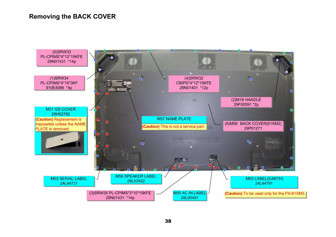
Removing the BACK COVER
(6)M58 BACK COVER(61XM2)29P01271
(6)M58 BACK COVER(61XM2)29P01271
M57 NAME PLATEM57 NAME PLATE
(2)M18 HANDLE29F00591 *2p
(2)M18 HANDLE29F00591 *2p
(1)SRW34 PL-CPIMS*4*16*3KF
910E4066 *4p
(1)SRW34 PL-CPIMS*4*16*3KF
910E4066 *4p
M55 AC IN LABEL29L00491
M55 AC IN LABEL29L00491
M03 SERIAL LABEL24L44731
M03 SERIAL LABEL24L44731
(5)SRW33 PL-CPIMS*4*12*15KFE
29N01431 *14p
(5)SRW33 PL-CPIMS*4*12*15KFE
29N01431 *14p
(3)SRW35 PL-CPIMS*3*10*15KFE29N01431 *14p
(3)SRW35 PL-CPIMS*3*10*15KFE29N01431 *14p
M56 SPEAKER LABEL29L03552
M56 SPEAKER LABEL29L03552
M31 GS COVER29H02782
M31 GS COVER29H02782
M63 LABEL(EARTH)24L44791
M63 LABEL(EARTH)24L44791
(Caution) To be used only for the PX-61XM3.(Caution) To be used only for the PX-61XM3.
(4)SRW32 CBIPS*4*12*15KFE
29N01401 *12p
(4)SRW32 CBIPS*4*12*15KFE
29N01401 *12p
(Caution) Replacement isimpossible unless the NAMEPLATE is removed.
(Caution) Replacement isimpossible unless the NAMEPLATE is removed. (Caution) This is not a service part.(Caution) This is not a service part.
38
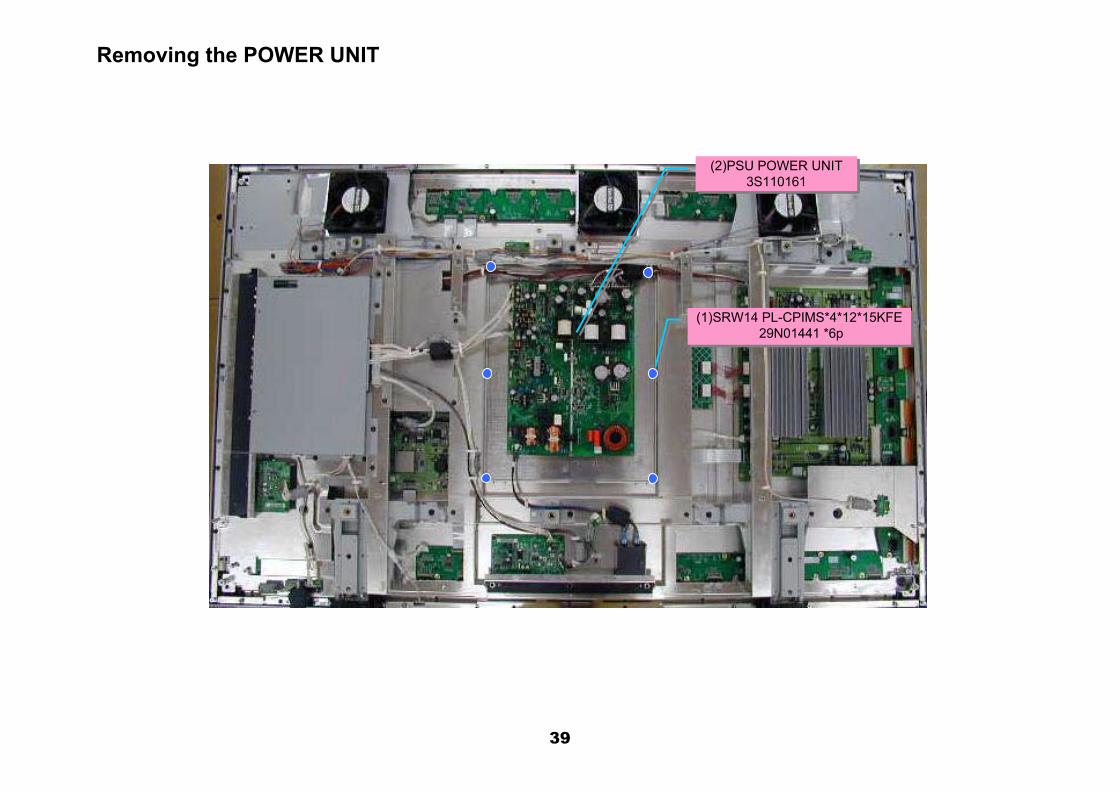
Removing the POWER UNIT
(1)SRW14 PL-CPIMS*4*12*15KFE29N01441 *6p
(1)SRW14 PL-CPIMS*4*12*15KFE29N01441 *6p
(2)PSU POWER UNIT3S110161
(2)PSU POWER UNIT3S110161
39
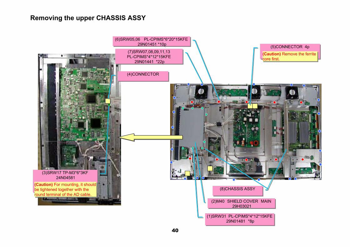
(2)M40 SHIELD COVER MAIN29H03021
(2)M40 SHIELD COVER MAIN29H03021
(1)SRW31 PL-CPIMS*4*12*15KFE29N01481 *8p
(1)SRW31 PL-CPIMS*4*12*15KFE29N01481 *8p
(3)SRW17 TP-M3*6*3KF24N04581
(3)SRW17 TP-M3*6*3KF24N04581
(Caution) For mounting, it shouldbe tightened together with the round terminal of the AD cable.
(Caution) For mounting, it shouldbe tightened together with the round terminal of the AD cable.
(4)CONNECTOR (4)CONNECTOR
(7)SRW07,08,09,11,13 PL-CPIMS*4*12*15KFE
29N01441 *22p
(7)SRW07,08,09,11,13 PL-CPIMS*4*12*15KFE
29N01441 *22p
(6)SRW05,06 PL-CPIMS*6*20*15KFE29N01451 *10p
(6)SRW05,06 PL-CPIMS*6*20*15KFE29N01451 *10p
Removing the upper CHASSIS ASSY
(5)CONNECTOR 4p(5)CONNECTOR 4p
(8)CHASSIS ASSY(8)CHASSIS ASSY
(Caution) Remove the ferrite core first.(Caution) Remove the ferrite core first.
40
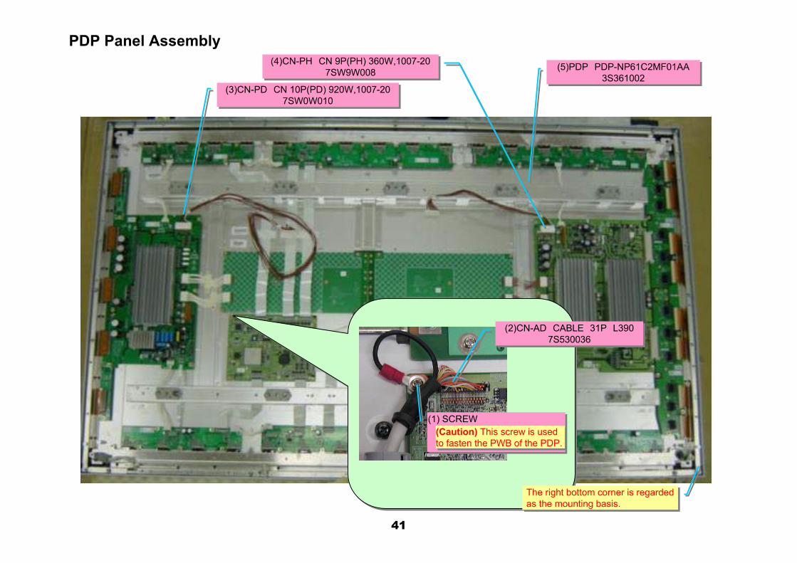
(1) SCREW(1) SCREW
(3)CN-PD CN 10P(PD) 920W,1007-207SW0W010
(3)CN-PD CN 10P(PD) 920W,1007-207SW0W010
(4)CN-PH CN 9P(PH) 360W,1007-207SW9W008
(4)CN-PH CN 9P(PH) 360W,1007-207SW9W008 (5)PDP PDP-NP61C2MF01AA
3S361002(5)PDP PDP-NP61C2MF01AA
3S361002
PDP Panel Assembly
(Caution) This screw is usedto fasten the PWB of the PDP.(Caution) This screw is usedto fasten the PWB of the PDP.
(2)CN-AD CABLE 31P L3907S530036
(2)CN-AD CABLE 31P L3907S530036
The right bottom corner is regarded as the mounting basis.The right bottom corner is regarded as the mounting basis.
41
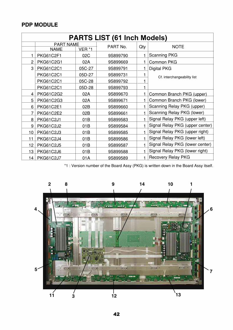
PARTS LIST (61 Inch Models)
NAME VER *1
1 PKG61C2F1 02C 9S899790 1 Scanning PKG
2 PKG61C2G1 02A 9S899669 1 Common PKG
3 PKG61C2C1 05C-27 9S899791 1 Digital PKG
Cf. interchangeability listPKG61C2C1 05D-27 9S899731 1
PKG61C2C1 05C-28 9S899792 1
PKG61C2C1 05D-28 9S899793 1
4 PKG61C2G2 02A 9S899670 1 Common Branch PKG (upper)Common Branch PKG (lower)Scanning Relay PKG (upper)
Scanning Relay PKG (lower)
Signal Relay PKG (upper left)
Signal Relay PKG (upper center)
Signal Relay PKG (upper right)
Signal Relay PKG (lower left)
Signal Relay PKG (lower center)
Signal Relay PKG (lower right)
Recovery Relay PKG
5 PKG61C2G3 02A 9S899671 1
6 PKG61C2E1 02B 9S899660 1
7 PKG61C2E2 02B 9S899661 1
8 PKG61C2J1 01B 9S899583 1
9 PKG61C2J2 01B 9S899584 1
10 PKG61C2J3 01B 9S899585 1
11 PKG61C2J4 01B 9S899586 1
12 PKG61C2J5 01B 9S899587 1
13 PKG61C2J6 01B 9S899588 1
14 PKG61C2J7 01A 9S899589 1
PART NAME PART No. Qty NOTE
PDP MODULE
3
12
4
5
6
7
8 9 10
11 12 13
14
*1 : Version number of the Board Assy (PKG) is written down in the Board Assy itself.
42
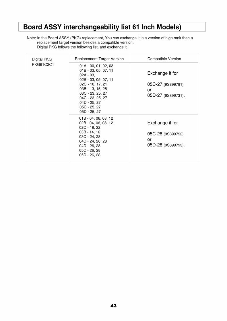
PKG61C2C1Digital PKG Replacement Target Version Compatible Version
01A - 00, 01, 02, 0301B - 03, 05, 07, 1102A - 03,02B - 03, 05, 07, 1102C - 10, 17, 2103B - 13, 15, 2503C - 23, 25, 2704C - 23, 25, 2704D - 25, 2705C - 25, 2705D - 25, 27
01B - 04, 06, 08, 1202B - 04, 06, 08, 1202C - 18, 2203B - 14, 1603C - 24, 2804C - 24, 26, 2804D - 26, 2805C - 26, 2805D - 26, 28
Board ASSY interchangeability list 61 Inch Models)Note:In the Board ASSY (PKG) replacement, You can exchange it in a version of high rank than a replacement target version besides a compatible version. Digital PKG follows the following list, and exchange it.
Exchange it for
05C-27 (9S899791)
or 05D-27 (9S899731).
Exchange it for
05C-28 (9S899792)
or 05D-28 (9S899793).
43
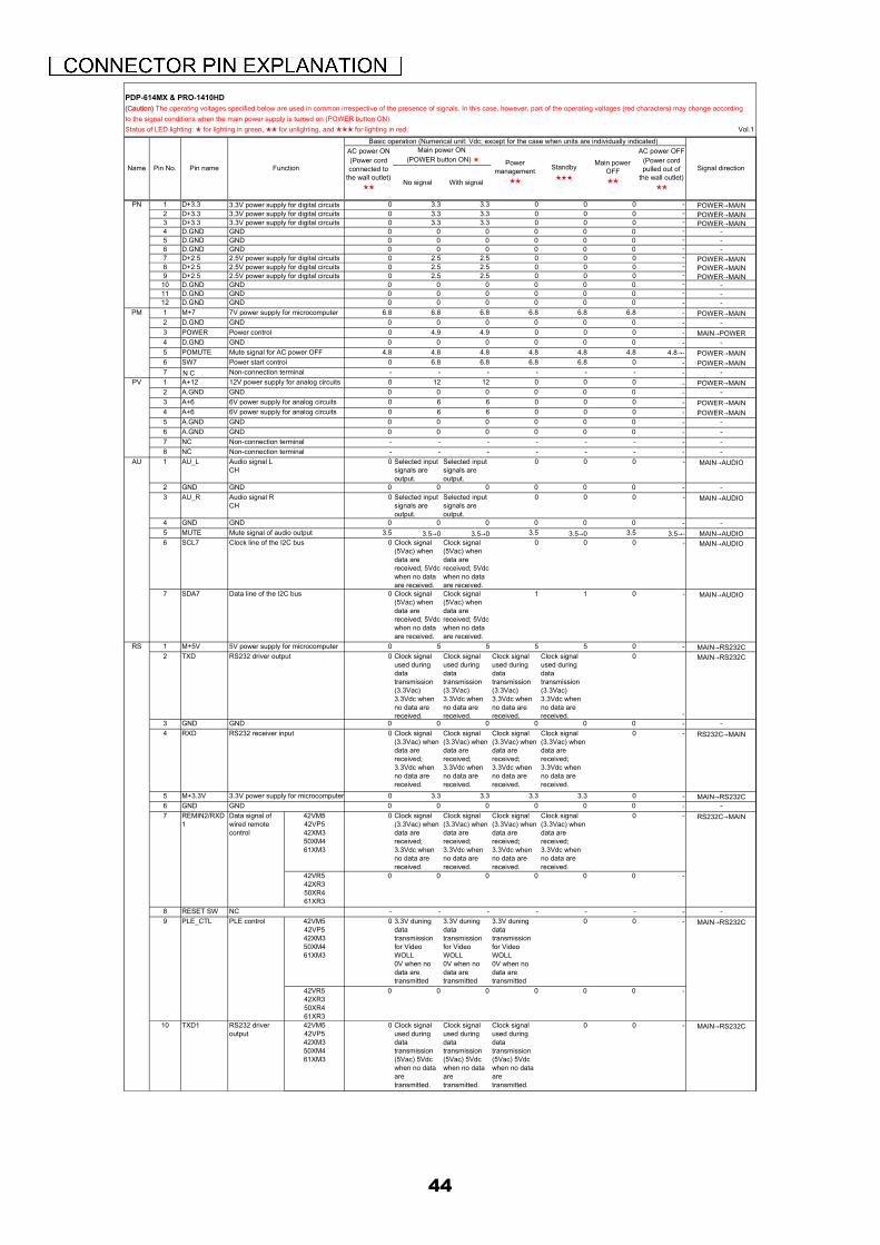
PDP-614MX & PRO-1410HD
No signal With signal
PN 1 D+3.3 0 3.3 3.3 0 0 0 - POWER→MAIN2 D+3.3 0 3.3 3.3 0 0 0 - POWER→MAIN3 D+3.3 0 3.3 3.3 0 0 0 - POWER→MAIN4 D.GND GND 0 0 0 0 0 0 - -5 D.GND GND 0 0 0 0 0 0 - -6 D.GND GND 0 0 0 0 0 0 - -7 D+2.5 0 2.5 2.5 0 0 0 - POWER→MAIN8 D+2.5 0 2.5 2.5 0 0 0 - POWER→MAIN9 D+2.5 0 2.5 2.5 0 0 0 - POWER→MAIN
10 D.GND GND 0 0 0 0 0 0 - -11 D.GND GND 0 0 0 0 0 0 - -12 D.GND GND 0 0 0 0 0 0 - -
PM 1 M+7 6.8 6.8 6.8 6.8 6.8 6.8 - POWER→MAIN2 D.GND GND 0 0 0 0 0 0 - -3 POWER Power control 0 4.9 4.9 0 0 0 - MAIN→POWER4 D.GND GND 0 0 0 0 0 0 - -5 POMUTE Mute signal for AC power OFF 4.8 4.8 4.8 4.8 4.8 4.8 4.8→- POWER→MAIN6 SW7 Power start control 0 6.8 6.8 6.8 6.8 0 - POWER→MAIN7 NC Non-connection terminal - - - - - - - -
PV 1 A+12 12V power supply for analog circuits 0 12 12 0 0 0 - POWER→MAIN2 A.GND GND 0 0 0 0 0 0 - -3 A+6 6V power supply for analog circuits 0 6 6 0 0 0 - POWER→MAIN4 A+6 6V power supply for analog circuits 0 6 6 0 0 0 - POWER→MAIN5 A.GND GND 0 0 0 0 0 0 - -6 A.GND GND 0 0 0 0 0 0 - -7 NC Non-connection terminal - - - - - - - -8 NC Non-connection terminal - - - - - - - -
AU 1 AU_L Audio signal LCH
0 Selected inputsignals areoutput.
Selected inputsignals areoutput.
0 0 0 - MAIN→AUDIO
2 GND GND 0 0 0 0 0 0 - -3 AU_R Audio signal R
CH0 Selected input
signals areoutput.
Selected inputsignals areoutput.
0 0 0 - MAIN→AUDIO
4 GND GND 0 0 0 0 0 0 - -5 MUTE Mute signal of audio output 3.5 3.5→0 3.5→0 3.5 3.5→0 3.5 3.5→- MAIN→AUDIO6 SCL7 Clock line of the I2C bus 0 Clock signal
(5Vac) whendata arereceived; 5Vdcwhen no dataare received.
Clock signal(5Vac) whendata arereceived; 5Vdcwhen no dataare received.
0 0 0 - MAIN→AUDIO
7 SDA7 Data line of the I2C bus 0 Clock signal(5Vac) whendata arereceived; 5Vdcwhen no dataare received.
Clock signal(5Vac) whendata arereceived; 5Vdcwhen no dataare received.
1 1 0 - MAIN→AUDIO
RS 1 M+5V 5V power supply for microcomputer 0 5 5 5 5 0 - MAIN→RS232C2 TXD RS232 driver output 0 Clock signal
used duringdatatransmission(3.3Vac)3.3Vdc whenno data arereceived.
Clock signalused duringdatatransmission(3.3Vac)3.3Vdc whenno data arereceived.
Clock signalused duringdatatransmission(3.3Vac)3.3Vdc whenno data arereceived.
Clock signalused duringdatatransmission(3.3Vac)3.3Vdc whenno data arereceived.
0
-
MAIN→RS232C
3 GND GND 0 0 0 0 0 0 - -4 RXD RS232 receiver input 0 Clock signal
(3.3Vac) whendata arereceived;3.3Vdc whenno data arereceived.
Clock signal(3.3Vac) whendata arereceived;3.3Vdc whenno data arereceived.
Clock signal(3.3Vac) whendata arereceived;3.3Vdc whenno data arereceived.
Clock signal(3.3Vac) whendata arereceived;3.3Vdc whenno data arereceived.
0 - RS232C→MAIN
5 M+3.3V 3.3V power supply for microcomputer 0 3.3 3.3 3.3 3.3 0 - MAIN→RS232C6 GND GND 0 0 0 0 0 0 - -7 REMIN2/RXD
1Data signal ofwired remotecontrol
42VM542VP542XM350XM461XM3
0 Clock signal(3.3Vac) whendata arereceived;3.3Vdc whenno data arereceived.
Clock signal(3.3Vac) whendata arereceived;3.3Vdc whenno data arereceived.
Clock signal(3.3Vac) whendata arereceived;3.3Vdc whenno data arereceived.
Clock signal(3.3Vac) whendata arereceived;3.3Vdc whenno data arereceived.
0 - RS232C→MAIN
42VR542XR350XR461XR3
0 0 0 0 0 0 -
8 RESET SW NC - - - - - - - -9 PLE_CTL PLE control 42VM5
42VP542XM350XM461XM3
0 3.3V duningdatatransmissionfor VideoWOLL0V when nodata aretransmitted
3.3V duningdatatransmissionfor VideoWOLL0V when nodata aretransmitted
3.3V duningdatatransmissionfor VideoWOLL0V when nodata aretransmitted
0 0 - MAIN→RS232C
42VR542XR350XR461XR3
0 0 0 0 0 0 -
10 TXD1 RS232 driveroutput
42VM542VP542XM350XM461XM3
0 Clock signalused duringdatatransmission(5Vac) 5Vdcwhen no dataaretransmitted.
Clock signalused duringdatatransmission(5Vac) 5Vdcwhen no dataaretransmitted.
Clock signalused duringdatatransmission(5Vac) 5Vdcwhen no dataaretransmitted.
0 0 - MAIN→RS232C
2.5V power supply for digital circuits
2.5V power supply for digital circuits
7V power supply for microcomputer
Signal direction
Main power ON (POWER button ON)
Pin No. Pin name Function Standby
Powermanagement
2.5V power supply for digital circuits
Main powerOFF
(Caution) The operating voltages specified below are used in common irrespective of the presence of signals. In this case, however, part of the operating voltages (red characters) may change accordingto the signal conditions when the main power supply is turned on (POWER button ON).Status of LED lighting: for lighting in green, for unlighting, and for lighting in red. Vol.1
3.3V power supply for digital circuits3.3V power supply for digital circuits3.3V power supply for digital circuits
AC power OFF(Power cordpulled out of
the wall outlet)
AC power ON(Power cordconnected to
the wall outlet)
Basic operation (Numerical unit: Vdc; except for the case when units are individually indicated)
Name
44

No signal With signal
Signal direction
Main power ON (POWER button ON)
Pin No. Pin name Function Standby
Powermanagement
Main powerOFF
AC power OFF(Power cordpulled out of
the wall outlet)
AC power ON(Power cordconnected to
the wall outlet)
Basic operation (Numerical unit: Vdc; except for the case when units are individually indicated)
Name
42VR542XR350XR461XR3
0 0 0 0 0 0 -
11 232C_SHUT ON/OFF control for TXD0 driver 0 3.3 3.3 3.3 3.3 0 - MAIN→RS232C12 REM Insertion
detection forwired remotecontrol input
42VM542VP542XM350XM461XM3
0 3.3V when awired remotecontrol isconnected/When notconnected.
3.3V when awired remotecontrol isconnected/When notconnected.
3.3V when awired remotecontrol isconnected/When notconnected.
3.3V when awired remotecontrol isconnected/When notconnected.
0 - RS232C→MAIN
42VR542XR350XR461XR3
- - - - - - - (NC for Model R)
TM 1 SCL5 Clock line of the I2C bus 0 Clock signalused duringdatatransmission(3.3Vac)3.3Vdc whenno data aretransmitted.
Clock signalused duringdatatransmission(3.3Vac)3.3Vdc whenno data aretransmitted.
0 0 0 - MAIN→SENB
2 GND GND 0 0 0 0 0 0 - -3 VDD+3.3V 3.3V power supply for analog signals 0 3.3 3.3 0 0 0 - MAIN→SENB4 SDA5 Data line of the I2C bus 0 During data
exchange:Clock signal(3.3Vac), Datanotexchanged:3.3Vdc
During dataexchange:Clock signal(3.3Vac), Datanotexchanged:3.3Vdc
0 0 0
-
MAIN←→SENB
TR 1 SCL5 Clock line of the I2C bus 0 Clock signalused duringdatatransmission(3.3Vac)3.3Vdc whenno data aretransmitted.
Clock signalused duringdatatransmission(3.3Vac)3.3Vdc whenno data aretransmitted.
0 0 0 - SENB→SEND
2 GND GND 0 0 0 0 0 0 - -3 VDD+3.3V 3.3V power supply for analog signals 0 3.3 3.3 0 0 0 - SENB→SEND4 SDA5 Data line of the I2C bus 0 During data
exchange:Clock signal(3.3Vac), Datanotexchanged:3.3Vdc
During dataexchange:Clock signal(3.3Vac), Datanotexchanged:3.3Vdc
0 0 0
-
SENB←→SEND
TS 1 SCL5 Clock line of the I2C bus 0 Clock signalused duringdatatransmission(3.3Vac)3.3Vdc whenno data aretransmitted.
Clock signalused duringdatatransmission(3.3Vac)3.3Vdc whenno data aretransmitted.
0 0 0 - SEND→SENC
2 GND GND 0 0 0 0 0 0 - -3 VDD+3.3V 3.3V power supply for analog signals 0 3.3 3.3 0 0 0 - SEND→SENC4 SDA5 Data line of the I2C bus 0 During data
exchange:Clock signal(3.3Vac), Datanotexchanged:3.3Vdc
During dataexchange:Clock signal(3.3Vac), Datanotexchanged:3.3Vdc
0 0 0
-
SEND←→SENC
FA 1 FAN-CTL Voltage-controllablepower supply
42VM542VP542VR5
- - - - - - - -
42XM342XR3
0 11.5Vdcduring high-speedrevolution(Fan mode H);8.5Vdc duringmedium speedrevolution(Fan mode M);6.5Vdc duringlow-speedrevolution(Fan mode L)
11.5Vdcduring high-speedrevolution(Fan mode H);8.5Vdc duringmedium speedrevolution(Fan mode M);6.5Vdc duringlow-speedrevolution(Fan mode L)
0 0 0 - MAIN→FAN
50XM450XR4
0 11.6Vdcduring high-speedrevolution(Fan mode H);7.8Vdc duringmedium speedrevolution(Fan mode M);5.3Vdc duringlow-speedrevolution(Fan mode L)
11.6Vdcduring high-speedrevolution(Fan mode H);7.8Vdc duringmedium speedrevolution(Fan mode M);5.3Vdc duringlow-speedrevolution(Fan mode L)
0 0 0 -
61XM361XR3
0 9.3Vdc duringhigh-speedrevolution(Fan mode H);7.6Vdc duringmedium speedrevolution(Fan mode M);5.3Vdc duringlow-speedrevolution(Fan mode L)
9.3Vdc duringhigh-speedrevolution(Fan mode H);7.6Vdc duringmedium speedrevolution(Fan mode M);5.3Vdc duringlow-speedrevolution(Fan mode L)
0 0 0 -
2 GND GND 0 0 0 0 0 0 - -3 ALARM 42VM5
42VP542VR5
- - - - - - - -FAN lock detectsignal output
45

No signal With signal
Signal direction
Main power ON (POWER button ON)
Pin No. Pin name Function Standby
Powermanagement
Main powerOFF
AC power OFF(Power cordpulled out of
the wall outlet)
AC power ON(Power cordconnected to
the wall outlet)
Basic operation (Numerical unit: Vdc; except for the case when units are individually indicated)
Name
42XM342XR350XM450XR461XM361XR3
0 0V duringnormal fanoperation;3.3Vdc while thefan is stopped.
0V duringnormal fanoperation;3.3Vdc while thefan is stopped.
0 0 0 - FAN→MAIN
FB 1 FAN-CTL Voltage-controllablepower supply
42VM542VP542VR5
- - - - - - - -
42XM342XR3
0 11.5Vdcduring high-speedrevolution(Fan mode H);8.5Vdc duringmedium speedrevolution(Fan mode M);6.5Vdc duringlow-speedrevolution(Fan mode L)
11.5Vdcduring high-speedrevolution(Fan mode H);8.5Vdc duringmedium speedrevolution(Fan mode M);6.5Vdc duringlow-speedrevolution(Fan mode L)
0 0 0 - MAIN→FAN
50XM450XR4
0 11.6Vdcduring high-speedrevolution(Fan mode H);7.8Vdc duringmedium speedrevolution(Fan mode M);5.3Vdc duringlow-speedrevolution(Fan mode L)
11.6Vdcduring high-speedrevolution(Fan mode H);7.8Vdc duringmedium speedrevolution(Fan mode M);5.3Vdc duringlow-speedrevolution(Fan mode L)
0 0 0 -
61XM361XR3
0 9.3Vdc duringhigh-speedrevolution(Fan mode H);7.6Vdc duringmedium speedrevolution(Fan mode M);5.3Vdc duringlow-speedrevolution(Fan mode L)
9.3Vdc duringhigh-speedrevolution(Fan mode H);7.6Vdc duringmedium speedrevolution(Fan mode M);5.3Vdc duringlow-speedrevolution(Fan mode L)
0 0 0 -
2 GND GND 0 0 0 0 0 0 - -3 ALARM 42VM5
42VP542VR5
- - - - - - - -
42XM342XR350XM450XR461XM361XR3
0 0V duringnormal fanoperation;3.3Vdc while thefan is stopped.
0V duringnormal fanoperation;3.3Vdc while thefan is stopped.
0 0 0 - FAN→MAIN
FC 1 FAN-CTL Voltage-controllablepower supply
42VM542VP542VR542XM342XR350XM450XR4
- - - - - - - -
61XM361XR3
0 9.3Vdc duringhigh-speedrevolution(Fan mode H);7.6Vdc duringmedium speedrevolution(Fan mode M);5.3Vdc duringlow-speedrevolution(Fan mode L)
9.3Vdc duringhigh-speedrevolution(Fan mode H);7.6Vdc duringmedium speedrevolution(Fan mode M);5.3Vdc duringlow-speedrevolution(Fan mode L)
0 0 0 - FAN→MAIN
2 GND GND 0 0 0 0 0 0 - -3 ALARM 42VM5
42VP542VR542XM342XR350XM450XR4
- - - - - - - -
61XM361XR3
0 0V duringnormal fanoperation;3.3Vdc while thefan is stopped.
0V duringnormal fanoperation;3.3Vdc while thefan is stopped.
0 0 0 - FAN→MAIN
AD 1 GND GND 0 0 0 0 0 0 - -2 GND GND 0 0 0 0 0 0 - -3 ALARM Module alarm signal 0 5Vdc during
normal PDPoperation; 0Vwhen the PDPis out of order.
5Vdc duringnormal PDPoperation; 0Vwhen the PDPis out of order.
0 0 0 - PDP→MAIN
4 GND GND 0 0 0 0 0 0 - -
FAN lock detectsignal output
FAN lock detectsignal output
46

No signal With signal
Signal direction
Main power ON (POWER button ON)
Pin No. Pin name Function Standby
Powermanagement
Main powerOFF
AC power OFF(Power cordpulled out of
the wall outlet)
AC power ON(Power cordconnected to
the wall outlet)
Basic operation (Numerical unit: Vdc; except for the case when units are individually indicated)
Name
5 PS+ PSS input PS+ 0 PSS LVDSserial differential PS+ input0Vac; Bias1.1Vdc
PSS LVDSserial differential PS+ input0.3Vac; Bias1.25Vdc
0 0 0 - PDP→MAIN
6 PS- PSS input PS- 0 PSS LVDSserial differential PS+ input0Vac; Bias1.4Vdc
PSS LVDSserial differential PS+ input0.3Vac; Bias1.25Vdc
0 0 0 - PDP→MAIN
7 MSEL 42V5 compatible interface OFF 0 0 0 0 0 0 - -8 GND GND 0 0 0 0 0 0 - -9 RH+ OSD system output H+ 0 OSD LVDS
serialdifferential H+output 0Vac;Bias 1.1Vdc
OSD LVDSserialdifferential H+output 0Vac;Bias 1.1Vdc
0 0 0 - MAIN→PDP
10 RH- OSD system output H– 0 OSD LVDSserialdifferential H-output 0Vac;Bias 1.4Vdc
OSD LVDSserialdifferential H-output 0Vac;Bias 1.4Vdc
0 0 0 - MAIN→PDP
11 RG+ OSD system output G+ 0 OSD LVDSserialdifferential G+output 0.3Vac;Bias 1.25Vdc
OSD LVDSserialdifferential G+output 0.3Vac;Bias 1.25Vdc
0 0 0 - MAIN→PDP
12 RG- OSD system output G- 0 OSD LVDSserialdifferential G-output 0.3Vac;Bias 1.25Vdc
OSD LVDSserialdifferential G-output 0.3Vac;Bias 1.25Vdc
0 0 0 - MAIN→PDP
13 RF+ Mode system output F+ 0 Video modeLVDS serialdifferential F+output 0.3Vac;Bias 1.25Vdc
Video modeLVDS serialdifferential F+output 0.3Vac;Bias 1.25Vdc
0 0 0 - MAIN→PDP
14 RF- Mode system output F- 0 Video modeLVDS serialdifferential F-output 0.3Vac;Bias 1.25Vdc
Video modeLVDS serialdifferential F-output 0.3Vac;Bias 1.25Vdc
0 0 0 - MAIN→PDP
15 GND GND 0 0 0 0 0 0 - -16 RE+ Video system output E+ 0 Video mode
LVDS serialdifferential E+output 0Vac;Bias 1.1Vdc
Video modeLVDS serialdifferential E+output 0Vac;Bias 1.1Vdc* Only for thePX-42VP4Series, 0.3Vacand bias 1.25Vdc in theatermode when60Hz motionpictures aredisplayed.
0 0 0 - MAIN→PDP
17 RE- Video system output E- 0 Video modeLVDS serialdifferential E-output 0Vac;Bias 1.4Vdc
Video modeLVDS serialdifferential E-output 0.3Vac;Bias 1.25Vdc* Only for thePX-42VP4Series, 0.3Vacand bias 1.25Vdc in theatermode when60Hz motionpictures aredisplayed.
0 0 0 - MAIN→PDP
18 RD+ Video system output D+ 0 Video modeLVDS serialdifferential D+output 0Vac;Bias 1.1Vdc
Video modeLVDS serialdifferential D+output 0.3Vac;Bias 1.25Vdc
0 0 0 - MAIN→PDP
19 RD- Video system output D– 0 Video modeLVDS serialdifferential D-output 0Vac;Bias 1.4Vdc
Video modeLVDS serialdifferential D-output 0.3Vac;Bias 1.25Vdc
0 0 0 - MAIN→PDP
47

No signal With signal
Signal direction
Main power ON (POWER button ON)
Pin No. Pin name Function Standby
Powermanagement
Main powerOFF
AC power OFF(Power cordpulled out of
the wall outlet)
AC power ON(Power cordconnected to
the wall outlet)
Basic operation (Numerical unit: Vdc; except for the case when units are individually indicated)
Name
20 RCLK+ Video system output clock+ 0 Video dataclock LVDSserialdifferentialclock+ output0.3Vac; Bias1.25Vdc
Video dataclock LVDSserialdifferentialclock+ output0.3Vac; Bias1.25Vdc
0 0 0 - MAIN→PDP
21 RCLK- Video system output clock– 0 Video dataclock LVDSserialdifferentialclock- output0.3Vac; Bias1.25Vdc
Video dataclock LVDSserialdifferentialclock- output0.3Vac; Bias1.25Vdc
0 0 0 - MAIN→PDP
22 GND GND 0 0 0 0 0 0 - -23 RC+ Video system output C+ 0 Video data
LVDS serialdifferential C+output 0.3Vac;Bias 1.25Vdc
Video dataLVDS serialdifferential C+output 0.3Vac;Bias 1.25Vdc
0 0 0 - MAIN→PDP
24 RC- Video system output C– 0 Video dataLVDS serialdifferential C-output 0.3Vac;Bias 1.25Vdc
Video dataLVDS serialdifferential C-output 0.3Vac;Bias 1.25Vdc
0 0 0 - MAIN→PDP
25 RB+ Video system output B+ 0 Video dataLVDS serialdifferential B+output 0Vac;Bias 1.1Vdc
Video dataLVDS serialdifferential B+output 0Vac;Bias 1.1Vdc
0 0 0 - MAIN→PDP
26 RB- Video system output B– 0 Video dataLVDS serialdifferential B-output 0Vac;Bias 1.4Vdc
Video dataLVDS serialdifferential B-output 0.3Vac;Bias 1.25Vdc
0 0 0 - MAIN→PDP
27 RA+ Video system output A+ 0 Video dataLVDS serialdifferential A+output 0Vac;Bias 1.1Vdc
Video dataLVDS serialdifferential A+output 0.3Vac;Bias 1.25Vdc
0 0 0 - MAIN→PDP
28 RA- Video system output A– 0 Video dataLVDS serialdifferential A-output 0Vac;Bias 1.4Vdc
Video dataLVDS serialdifferential A-output 0.3Vac;Bias 1.25Vdc
0 0 0 - MAIN→PDP
29 GND GND 0 0 0 0 0 0 - -30 GND GND 0 0 0 0 0 0 - -31 GND GND 0 0 0 0 0 0 - -
LD 1 REMIN1 Infrared remote control data 0 Clock signal(5Vac) whendata arereceived; 5Vdcwhen no dataare received.
Clock signal(5Vac) whendata arereceived; 5Vdcwhen no dataare received.
Clock signal(5Vac) whendata arereceived; 5Vdcwhen no dataare received.
Clock signal(5Vac) whendata arereceived; 5Vdcwhen no dataare received.
0
-
LED→PWR
2 LEDCTL1 Standby red LED control 0 0 0 3.3 3.3 0 - PWR→LED3 LEDCTL2 POWER ON green LED control 0 3.3 3.3 0 0 0 - PWR→LED4 GND GND 0 0 0 0 0 0 - -5 M+5V 5V power supply for microcomputer 0 5 5 5 5 0 - PWR→LED
PW 1 SW7 Power start control 0 6.8 6.8 6.8 6.8 0 - PW→MAIN2 POIN Power start detection 0 3.3 3.3 3.3 3.3 0 - PW→MAIN3 GND GND 0 0 0 0 0 0 - -4 M+5V 5V power supply for microcomputer 0 5 5 5 5 0 - MAIN→PW5 M+7V 7V power supply for microcomputer 0 6.8 6.8 6.8 6.8 6.8 - MAIN→PW6 REMIN1 Infrared remote control data 0 Clock signal
(5Vac) whendata arereceived; 5Vdcwhen no dataare received.
Clock signal(5Vac) whendata arereceived; 5Vdcwhen no dataare received.
Clock signal(5Vac) whendata arereceived; 5Vdcwhen no dataare received.
Clock signal(5Vac) whendata arereceived; 5Vdcwhen no dataare received.
0 - PW→MAIN
7 LEDCTL1 Standby red LED control 0 0 0 3.3 3.3 0 - MAIN→PW8 LEDCTL2 POWER ON green LED control 0 3.3 3.3 0 0 0 - MAIN→PW
SW 1 CTL1 Key input detection 0 0.7~2.8Vdcwhen keyinputs areentered;3.3Vdc whenno key inputsare entered.
0.7~2.8Vdcwhen keyinputs areentered;3.3Vdc whenno key inputsare entered.
0.7~2.8Vdcwhen keyinputs areentered;3.3Vdc whenno key inputsare entered.
0.7~2.8Vdcwhen keyinputs areentered;3.3Vdc whenno key inputsare entered.
0 - SW→MAIN
2 CTL2 Key input detection 0 0.7~2.8Vdcwhen keyinputs areentered;3.3Vdc whenno key inputsare entered.
0.7~2.8Vdcwhen keyinputs areentered;3.3Vdc whenno key inputsare entered.
0.7~2.8Vdcwhen keyinputs areentered;3.3Vdc whenno key inputsare entered.
0.7~2.8Vdcwhen keyinputs areentered;3.3Vdc whenno key inputsare entered.
0 - SW→MAIN
3 GND GND 0 0 0 0 0 0 - -PA 1 S+12 +12V power supply for audio circuits 0 12 12 0 0 0 - POWER→AUDIO
2 S+12 +12V power supply for audio circuits 0 12 12 0 0 0 - POWER→AUDIO3 S+12 +12V power supply for audio circuits 0 12 12 0 0 0 - POWER→AUDIO4 GND GND 0 0 0 0 0 0 - -
48
No signal With signal
Signal direction
Main power ON (POWER button ON)
Pin No. Pin name Function Standby
Powermanagement
Main powerOFF
AC power OFF(Power cordpulled out of
the wall outlet)
AC power ON(Power cordconnected to
the wall outlet)
Basic operation (Numerical unit: Vdc; except for the case when units are individually indicated)
Name
5 GND GND 0 0 0 0 0 0 - -6 GND GND 0 0 0 0 0 0 - -
PD 1 ALARM PDP alarm signal 0 5Vdc when thePDP is normal;0V when it isabnormal.
5Vdc when thePDP is normal;0V when it isabnormal.
0 0 0 - PDP→POWER
2 D.GND GND 0 0 0 0 0 0 - -3 D.GND GND 0 0 0 0 0 0 - -4 D.GND GND 0 0 0 0 0 0 - -5 D.GND GND 0 0 0 0 0 0 - -6 D+60 Vd power supply
for PDP0 60Vdc
(changeableaccording tothe PDP)
60Vdc(changeableaccording tothe PDP)
0 0 0 - PDWER→PDP
7 D+60 digital circuits 0 60Vdc(changeableaccording tothe PDP)
60Vdc(changeableaccording tothe PDP)
0 0 0 - PDWER→PDP
8 NC digital circuits - - - - - - - -9 D+170 Vs power supply
for PDP high-voltage circuits
0 170Vdc(changeableaccording tothe PDP)
170Vdc(changeableaccording tothe PDP)
0 0 0
-
PDWER→PDP
10 D+170 Vs power supplyfor PDP high-voltage circuits
0 170Vdc(changeableaccording tothe PDP)
170Vdc(changeableaccording tothe PDP)
0 0 0 - PDWER→PDP
1 ALARM PDP alarm signal 0 5Vdc when thePDP is normal;0V when it isabnormal.
5Vdc when thePDP is normal;0V when it isabnormal.
0 0 0 - PDP→POWER
2 D.GND GND 0 0 0 0 0 0 - -3 D.GND GND 0 0 0 0 0 0 - -4 D+5 5V power supply
for digital circuits0 5.15 5.15 0 0 0
-POWER→PDP
5 D.GND GND 0 0 0 0 0 0 - -6 D.GND GND 0 0 0 0 0 0 - -7 D+65 Vd power supply
for PDP0 65Vdc
(changeableaccording tothe PDP)
65Vdc(changeableaccording tothe PDP)
0 0 0 - POWER→PDP
8 NC digital circuits - - - - - - - -9 D+175 Vs power supply
for PDP high-voltage circuits
0 175Vdc(changeableaccording tothe PDP)
175Vdc(changeableaccording tothe PDP)
0 0 0
-
POWER→PDP
10 D+175 Vs power supplyfor PDP high-voltage circuits
0 175Vdc(changeableaccording tothe PDP)
175Vdc(changeableaccording tothe PDP)
0 0 0 - POWER→PDP
PH 1 D+5 5V power supplyfor digital circuits
0 5.15 5.15 0 0 0-
PDWER→PDP
2 D+5 5V power supplyfor digital circuits
0 5.15 5.15 0 0 0-
PDWER→PDP
3 D.GND GND 0 0 0 0 0 0 - -4 D.GND GND 0 0 0 0 0 0
--
1 D+175 Vs power supplyfor PDP high-voltage circuits
0 175Vdc(changeableaccording tothe PDP)
175Vdc(changeableaccording tothe PDP)
0 0 0
-
POWER→PDP
2 D+175 Vs power supplyfor PDP high-voltage circuits
0 175Vdc(changeableaccording tothe PDP)
175Vdc(changeableaccording tothe PDP)
0 0 0
-
POWER→PDP
3 NC Non-connection - - - - - - - -4 D+65 Vd power supply
for PDP0 65Vdc
(changeableaccording tothe PDP)
65Vdc(changeableaccording tothe PDP)
0 0 0
-
POWER→PDP
5 D.GND digital circuits 0 0 0 0 0 0 - -6 D.GND GND 0 0 0 0 0 0 - -7 D+5 5V power supply
for digital circuits0 5.15 5.15 0 0 0
-POWER→PDP
8 D.GND GND 0 0 0 0 0 0 - -9 D.GND GND 0 0 0 0 0 0 - -
61XM361XR3
42VM542VP542VR542XM342XR350XM450XR4
61XM361XR3
42VM542VP542VR542XM342XR350XM450XR4
49
42 Inch Section (PDP-424MV)
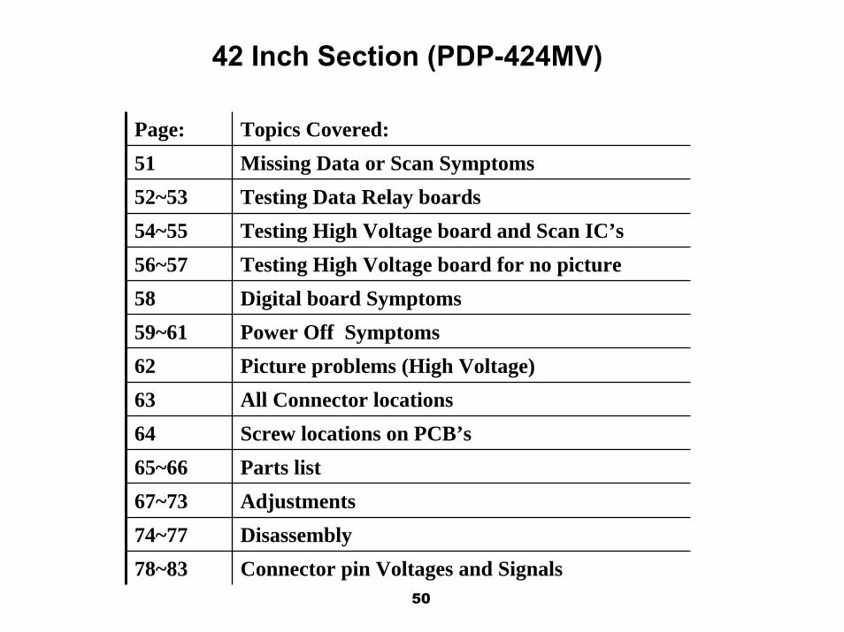
Page: Topics Covered:51 Missing Data or Scan Symptoms52~53 Testing Data Relay boards54~55 Testing High Voltage board and Scan IC’s56~57 Testing High Voltage board for no picture58 Digital board Symptoms59~61 Power Off Symptoms62 Picture problems (High Voltage)63 All Connector locations64 Screw locations on PCB’s65~66 Parts list67~73 Adjustments74~77 Disassembly78~83 Connector pin Voltages and Signals
50
NEC Plasma Display
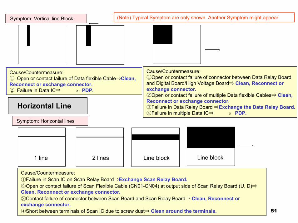
Symptom: Vertical line Block
Cause/Countermeasure:① Open or contact failure of Data flexible Cable⇒Clean, Reconnect or exchange connector.② Failure in Data IC⇒Replace PDP.
Cause/Countermeasure:①Open or contact failure of connector between Data Relay Board and Digital Board/High Voltage Board⇒ Clean, Reconnect or exchange connector.②Open or contact failure of multiple Data flexible Cables⇒ Clean, Reconnect or exchange connector.③Failure in Data Relay Board ⇒Exchange the Data Relay Board.④Failure in multiple Data IC⇒Replace PDP.
Horizontal Line
1 line 2 lines Line block Line block
Symptom: Horizontal lines
Cause/Countermeasure: ①Failure in Scan IC on Scan Relay Board⇒Exchange Scan Relay Board.②Open or contact failure of Scan Flexible Cable (CN01-CN04) at output side of Scan Relay Board (U, D)⇒Clean, Reconnect or exchange connector.③Contact failure of connector between Scan Board and Scan Relay Board⇒ Clean, Reconnect or exchange connector.④Short between terminals of Scan IC due to screw dust⇒ Clean around the terminals.
(Note) Typical Symptom are only shown. Another Symptom might appear.
51
NEC Plasma Display
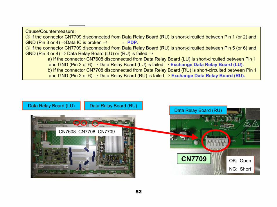
Cause/Countermeasure:② If the connector CN7709 disconnected from Data Relay Board (RU) is short-circuited between Pin 1 (or 2) and GND (Pin 3 or 4) ⇒Data IC is broken ⇒Replace PDP.③ If the connector CN7709 disconnected from Data Relay Board (RU) is short-circuited between Pin 5 (or 6) and GND (Pin 3 or 4) ⇒ Data Relay Board (LU) or (RU) is failed ⇒ a) If the connector CN7608 disconnected from Data Relay Board (LU) is short-circuited between Pin 1
and GND (Pin 2 or 6) ⇒ Data Relay Board (LU) is failed ⇒ Exchange Data Relay Board (LU). b) If the connector CN7708 disconnected from Data Relay Board (RU) is short-circuited between Pin 1
and GND (Pin 2 or 6) ⇒ Data Relay Board (RU) is failed ⇒ Exchange Data Relay Board (RU).
Data Relay Board (RU)Data Relay Board (LU)
CN7709
Data Relay Board (RU)
OK: Open
NG: Short
CN7608 CN7708 CN7709
52
NEC Plasma Display
Cause/ Countermeasure :④ If the connector CN7909 disconnected from Data Relay Board (RD) is short-circuited between Pin 1 (or 2) and GND (Pin 3 or 4) ⇒Data IC is broken ⇒Repair PDP. ⑤ If the connector CN7909 disconnected from Data Relay Board (RD) is short-circuited between Pin 5 (or 6) and GND (Pin 3 or 4) ⇒ Data Relay Board (LD) or (RD) is failed ⇒ a) If the connector CN7808 disconnected from Data Relay Board (LD) is short-circuited between Pin 8
and GND (Pin 3 or 7) ⇒ Data Relay Board (LD) is failed ⇒ Exchange Data Relay Board (LD). b) If the connector CN7908 disconnected from Data Relay Board (RD) is short-circuited between Pin 8
and GND (Pin 3 or 7) ⇒ Data Relay Board (RD) is failed ⇒ Exchange Data Relay Board (RD).
OK: Open
NG: ShortData Relay Board (RD)
CN7909
Data Relay Board (RD)Data Relay Board (LD)
CN7808 CN7908 CN7909
53
NEC Plasma Display
Symptom:No Picture. (Priming doesn’t flash if W-X terminals are short-circuited.)
Checkpoints
PH2401F
Cause/Countermeasure: No Diode characteristic ⇒ Exchange High Voltage Board.
PH2401F
High Voltage Board; Surface
High Voltage Board; Reverse
K(57~59)
L(61~64)
M(66~69)
N(71~74)
O(76~78)
P(81~84)
Q(86~89)
R(91)
S(93~96)
T(99~103)
V(107)
W(109)X(112)
J(55~56)
D(15~18)
F(33~35)
C(10~13)
A(1~4)
B(6~9)
E(24)
G(39~40)
H(49~50)
I(53)OK: Diode characteristic NG: Other than above
A-D M-LA-E N-PB-D O-PC-D Q-RE-R R-SF-N R-TG-M S-TH-I T-VI-J W-XK-L
54
NEC Plasma Display
Scan Relay Board (U)
Cause/Countermeasure: If short-circuited, disconnect connector between High Voltage Board and Scan Relay Board and,④ Short between NEGA-POSI on High Voltage Board ⇒ Exchange High Voltage Board.⑤ Short between NEGA-POSI on Scan Relay Board (U)
⇒ Exchange Scan Relay Board (U).⑥Short between NEGA-POSI on Scan Relay Board (D)
⇒ Exchange Scan Relay Board (D). CheckpointNEGA-POSI
OK: More than kΩNG: Short
High Voltage Board
CheckpointNEGA-POSI
NEGA
NEGA
POSI
POSI
OK: More than kΩNG: Short
High Voltage Board Scan Relay Board (D)
55
NEC Plasma Display
Picture DefectHigh Voltage Board
OK: Short
NG: Open
Glass Fuse (F302)(Note) Typical symptom are only shown. Another Symptom might appear.
Symptom:No Picture(Priming flash).
Cause/Countermeasure: ①F302 open⇒Exchange High Voltage Board.
56
NEC Plasma Display
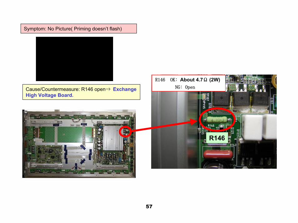
Symptom: No Picture( Priming doesn’t flash)
Cause/Countermeasure: R146 open⇒ Exchange High Voltage Board.
R146
R146 OK: About 4.7Ω (2W) NG: Open
57
NEC Plasma Display
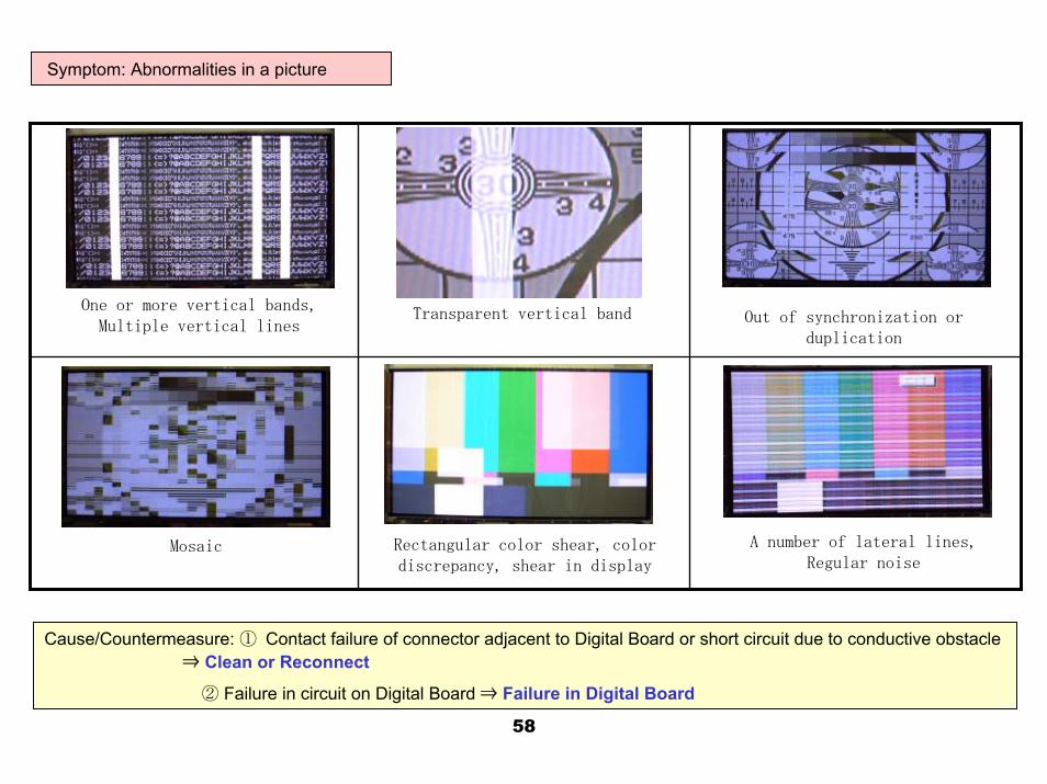
Symptom: Abnormalities in a picture
One or more vertical bands,Multiple vertical lines
Transparent vertical band Out of synchronization or duplication
A number of lateral lines,Regular noise
Rectangular color shear, color discrepancy, shear in display
Mosaic
Cause/Countermeasure: ① Contact failure of connector adjacent to Digital Board or short circuit due to conductive obstacle ⇒ Clean or Reconnect
② Failure in circuit on Digital Board ⇒ Failure in Digital Board
58
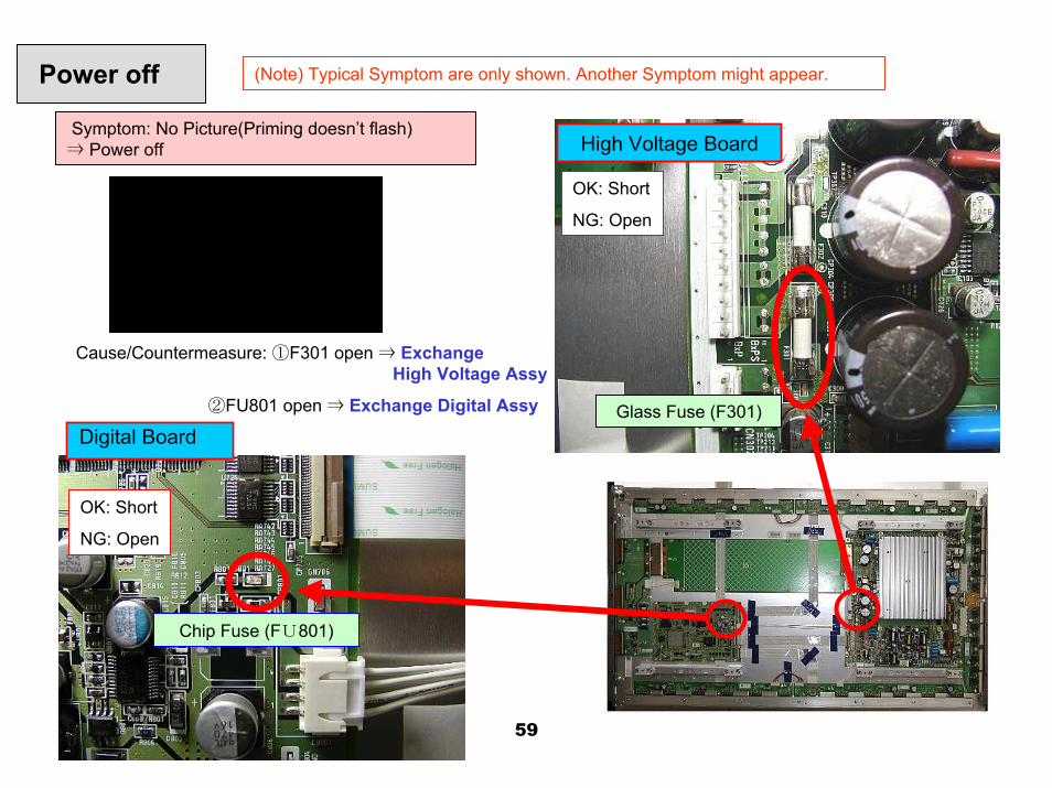
NEC Plasma Display
Cause/Countermeasure: ①F301 open ⇒ Exchange High Voltage Assy
②FU801 open ⇒ Exchange Digital Assy .
Power off (Note) Typical Symptom are only shown. Another Symptom might appear.
OK: Short
NG: Open
Glass Fuse (F301)
Chip Fuse (FU801)
OK: Short
NG: Open
Symptom: No Picture(Priming doesn’t flash) ⇒ Power off
Digital Board
High Voltage Board
59
NEC Plasma Display
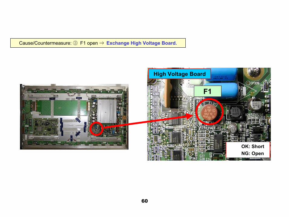
Cause/Countermeasure: ③ F1 open ⇒ Exchange High Voltage Board.
OK: Short NG: Open
High Voltage Board
F1
60
NEC Plasma Display
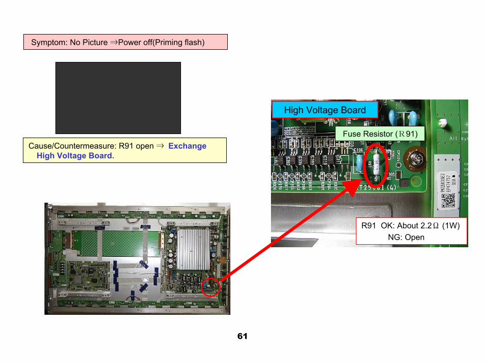
Symptom: No Picture ⇒Power off(Priming flash)
高圧PKG
Fuse Resistor (R91)Cause/Countermeasure: R91 open ⇒ Exchange High Voltage Board.
High Voltage Board
R91 OK: About 2.2Ω (1W) NG: Open
61
NEC Plasma Display
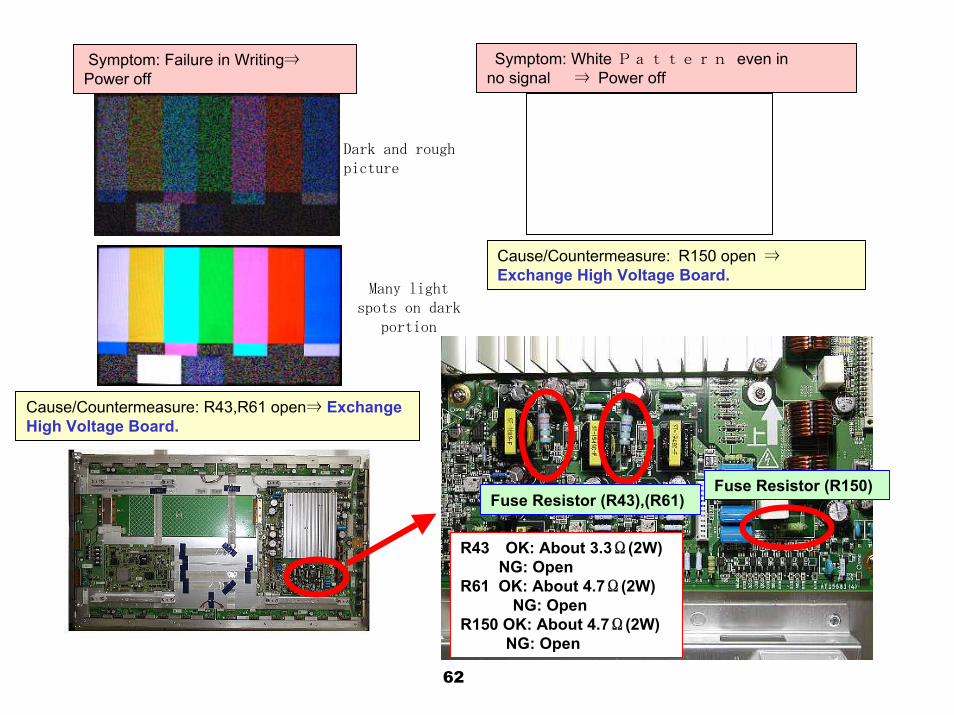
Dark and rough picture
Many light spots on dark
portion
Fuse Resistor (R43),(R61)Fuse Resistor (R150)
Symptom: Failure in Writing⇒Power off
Cause/Countermeasure: R43,R61 open⇒ Exchange High Voltage Board.
Symptom: White Pattern even in no signal ⇒ Power off
Cause/Countermeasure: R150 open ⇒Exchange High Voltage Board.
R43 OK: About 3.3Ω(2W) NG: OpenR61 OK: About 4.7Ω(2W) NG: Open
R150 OK: About 4.7Ω(2W) NG: Open
62
NEC Plasma Display
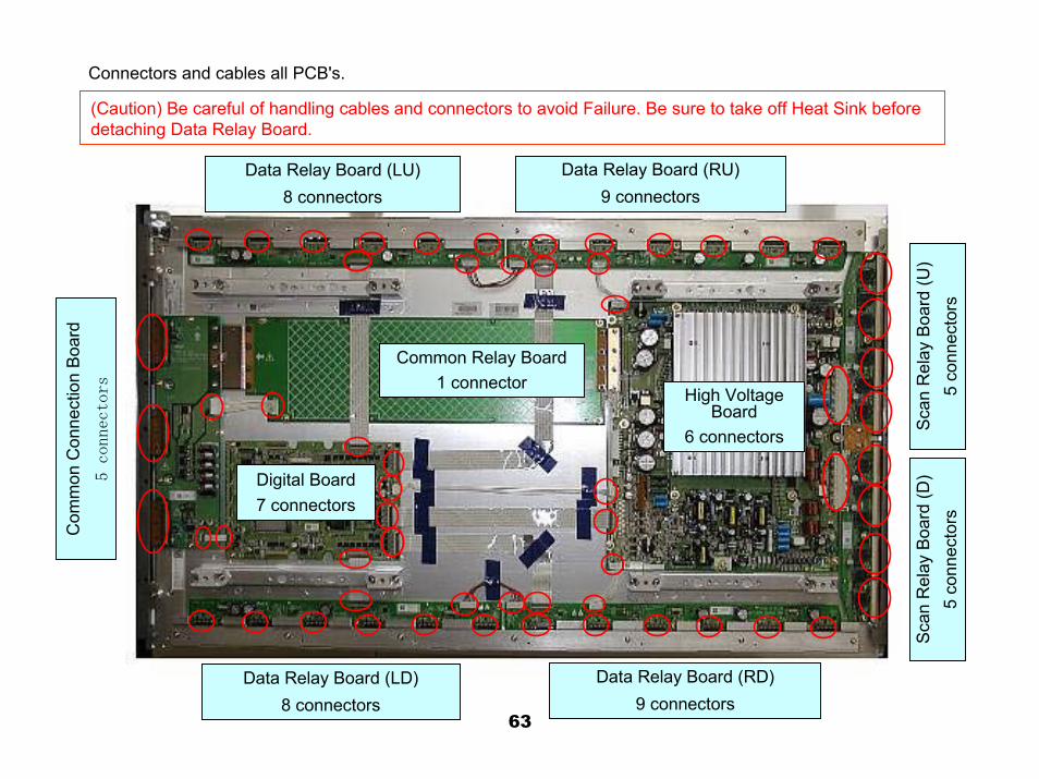
(Caution) Be careful of handling cables and connectors to avoid Failure. Be sure to take off Heat Sink before detaching Data Relay Board.
Connectors and cables all PCB's.
Data Relay Board (LD)8 connectors
Data Relay Board (LU)8 connectors
Data Relay Board (RU)9 connectors
Digital Board7 connectors
Common Relay Board1 connector
High Voltage Board
6 connectors
Data Relay Board (RD)9 connectors
Scan
Rel
ay B
oard
(D)
5 co
nnec
tors
Scan
Rel
ay B
oard
(U)
5 co
nnec
tors
Com
mon
Con
nect
ion
Boa
rd5 connectors
63
NEC Plasma Display
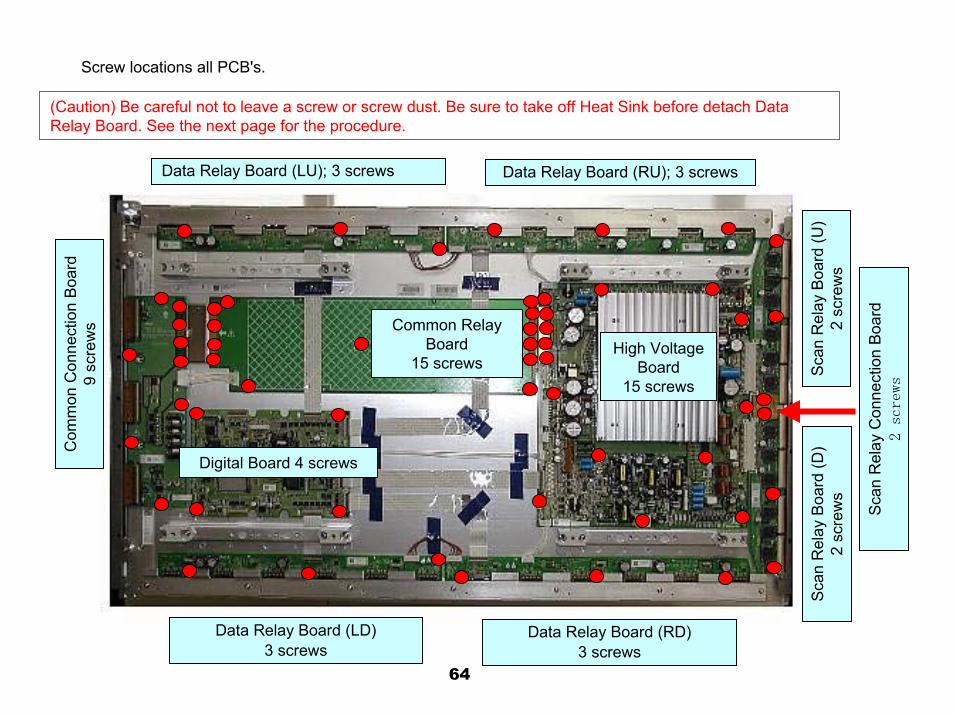
Screw locations all PCB's.
(Caution) Be careful not to leave a screw or screw dust. Be sure to take off Heat Sink before detach Data Relay Board. See the next page for the procedure.
Scan
Rel
ay C
onne
ctio
n Bo
ard
2 screws
Data Relay Board (LD)3 screws
Data Relay Board (RD)3 screws
Data Relay Board (RU); 3 screws
Common Relay Board
15 screws
Digital Board 4 screws
Com
mon
Con
nect
ion
Boa
rd9
scre
ws
Sca
n R
elay
Boa
rd (D
) 2
scre
ws
Scan
Rel
ay B
oard
(U)
2 sc
rew
s
High Voltage Board
15 screws
Data Relay Board (LU); 3 screws
64
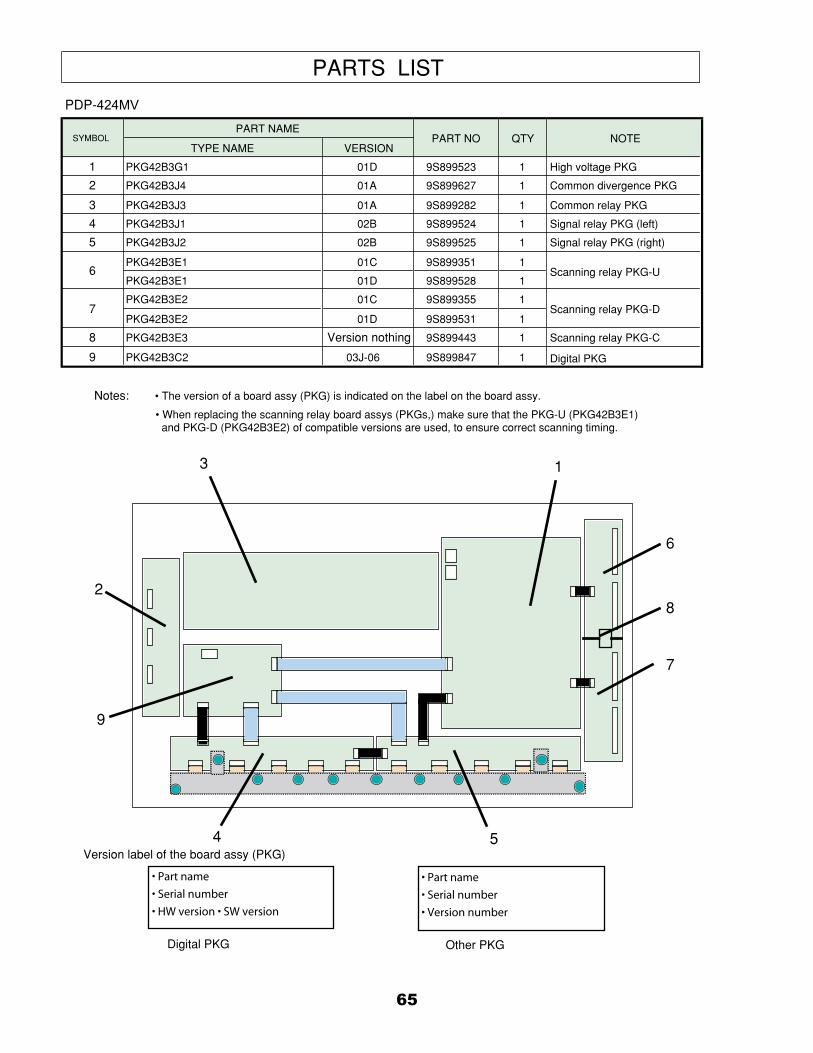
PDP-424MV
TYPE NAME VERSION
1 PKG42B3G1 01D 9S899523 1 High voltage PKG
2 PKG42B3J4 01A 9S899627 1 Common divergence PKG
3 PKG42B3J3 01A 9S899282 1 Common relay PKG
4 PKG42B3J1 02B 9S899524 1 Signal relay PKG (left)
5 PKG42B3J2 02B 9S899525 1 Signal relay PKG (right)
PKG42B3E1 01C 9S899351 1
PKG42B3E1 01D 9S899528 1
PKG42B3E2 01C 9S899355 1
PKG42B3E2 01D 9S899531 1
8 PKG42B3E3 Version nothing 9S899443 1 Scanning relay PKG-C
9 PKG42B3C2 03J-06 9S899847 1 Digital PKG
Notes: • The version of a board assy (PKG) is indicated on the label on the board assy.
• When replacing the scanning relay board assys (PKGs,) make sure that the PKG-U (PKG42B3E1) and PKG-D (PKG42B3E2) of compatible versions are used, to ensure correct scanning timing.
Version label of the board assy (PKG)
Digital PKG Other PKG
6 Scanning relay PKG-U
7 Scanning relay PKG-D
PARTS LIST
SYMBOLPART NAME
PART NO QTY NOTE
3
2
1
6
7
4 5
8
9
• Part name
• Serial number
• Version number
• Part name
• Serial number
• HW version • SW version
65
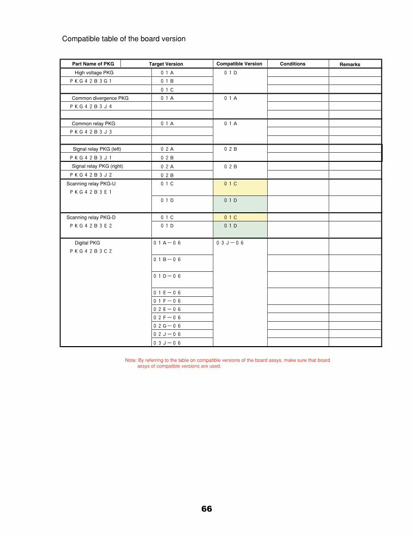
Compatible table of the board version
Part Name of PKG Target Version Compatible Version Conditions Remarks
High voltage PKG
Common divergence PKG
Common relay PKG
Signal relay PKG (left)
Signal relay PKG (right)
Scanning relay PKG-U
Scanning relay PKG-D
Digital PKG
Note: By referring to the table on compatible versions of the board assys, make sure that board assys of compatible versions are used.
66
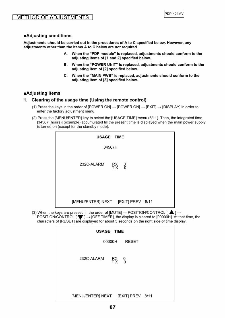
Adjusting conditions Adjustments should be carried out in the procedures of A to C specified below. However, any adjustments other than the items A to C below are not required.
A. When the “PDP module” is replaced, adjustments should conform to the adjusting items of [1 and 2] specified below.
B. When the “POWER UNIT” is replaced, adjustments should conform to the adjusting item of [2] specified below.
C. When the “MAIN PWB” is replaced, adjustments should conform to the adjusting item of [3] specified below.
Adjusting items 1. Clearing of the usage time (Using the remote control)
(1) Press the keys in the order of [POWER ON] → [POWER ON] → [EXIT] → [DISPLAY] in order to enter the factory adjustment menu.
(2) Press the [MENU/ENTER] key to select the [USAGE TIME] menu (8/11). Then, the integrated time [34567 (hours)] (example) accumulated till the present time is displayed when the main power supply is turned on (except for the standby mode).
(3) When the keys are pressed in the order of [MUTE] → POSITION/CONTROL [ ] →
POSITION/CONTROL [ ] → [OFF TIMER], the display is cleared to [00000H]. At that time, the characters of [RESET] are displayed for about 5 seconds on the right side of time display.
USAGE TIME 34567H 232C-ALARM RX 0
T X 0
[MENU/ENTER] NEXT [EXIT] PREV 8/11
USAGE TIME 00000H RESET 232C-ALARM RX 0
T X 0
[MENU/ENTER] NEXT [EXIT] PREV 8/11
67
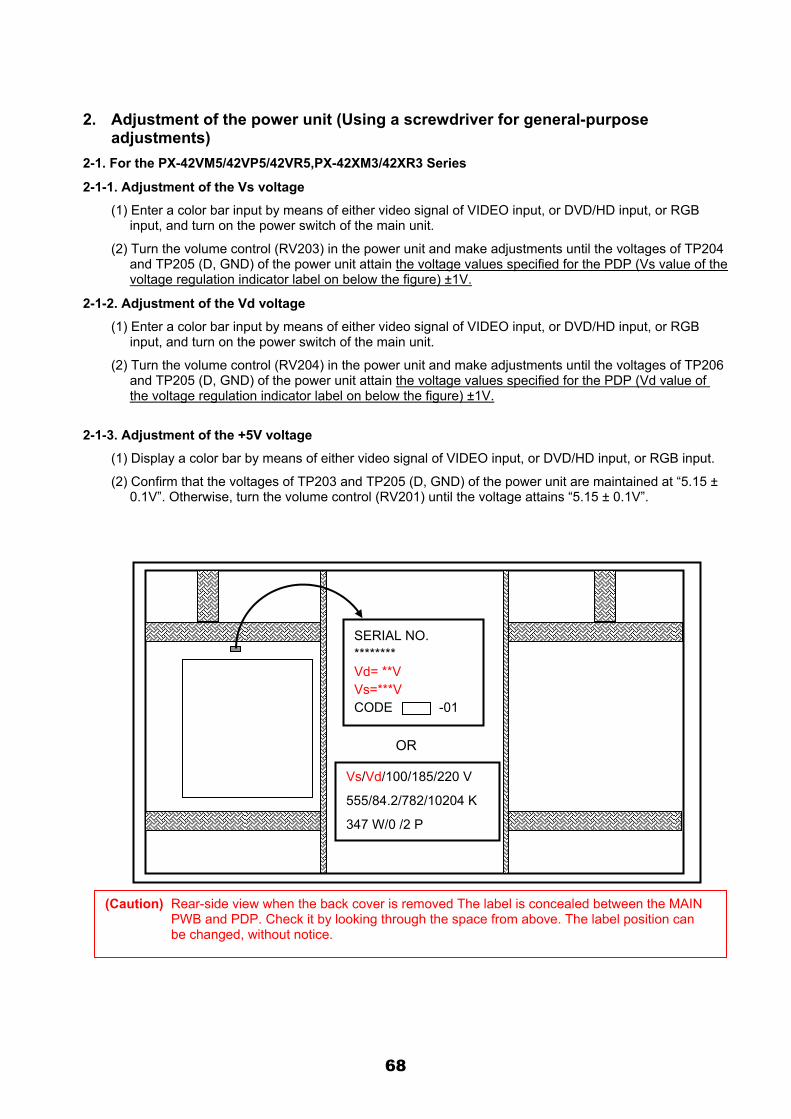
2. Adjustment of the power unit (Using a screwdriver for general-purpose
adjustments) 2-1. For the PX-42VM5/42VP5/42VR5,PX-42XM3/42XR3 Series
2-1-1. Adjustment of the Vs voltage
(1) Enter a color bar input by means of either video signal of VIDEO input, or DVD/HD input, or RGB input, and turn on the power switch of the main unit.
(2) Turn the volume control (RV203) in the power unit and make adjustments until the voltages of TP204 and TP205 (D, GND) of the power unit attain the voltage values specified for the PDP (Vs value of the voltage regulation indicator label on below the figure) ±1V.
2-1-2. Adjustment of the Vd voltage
(1) Enter a color bar input by means of either video signal of VIDEO input, or DVD/HD input, or RGB input, and turn on the power switch of the main unit.
(2) Turn the volume control (RV204) in the power unit and make adjustments until the voltages of TP206 and TP205 (D, GND) of the power unit attain the voltage values specified for the PDP (Vd value of the voltage regulation indicator label on below the figure) ±1V.
2-1-3. Adjustment of the +5V voltage
(1) Display a color bar by means of either video signal of VIDEO input, or DVD/HD input, or RGB input.
(2) Confirm that the voltages of TP203 and TP205 (D, GND) of the power unit are maintained at “5.15 ± 0.1V”. Otherwise, turn the volume control (RV201) until the voltage attains “5.15 ± 0.1V”.
(Caution) Rear-side view when the back cover is removed The label is concealed between the MAIN PWB and PDP. Check it by looking through the space from above. The label position can be changed, without notice.
SERIAL NO. ******** Vd= **V Vs=***V CODE -01
Vs/Vd/100/185/220 V
555/84.2/782/10204 K
347 W/0 /2 P
OR
68
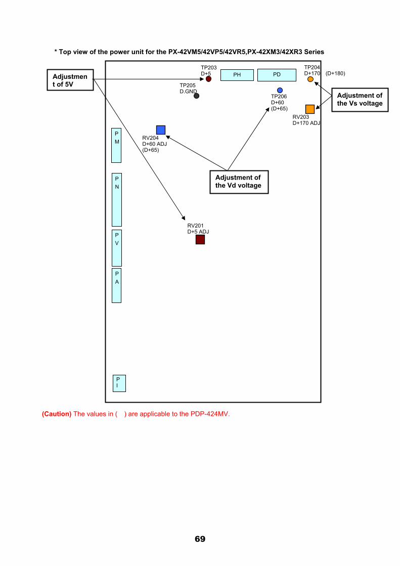
* Top view of the power unit for the PX-42VM5/42VP5/42VR5,PX-42XM3/42XR3 Series
(Caution) The values in ( ) are applicable to the PDP-424MV.
PH
PV
TP203 D+5
TP206 D+60 (D+65)
TP204 D+170 (D+180)
RV204 D+60 ADJ(D+65)
RV203 D+170 ADJ
PA
PM
PD
P I
PN
TP205 D.GND
RV201 D+5 ADJ
Adjustment of 5V
Adjustment of the Vd voltage
Adjustment of the Vs voltage
69
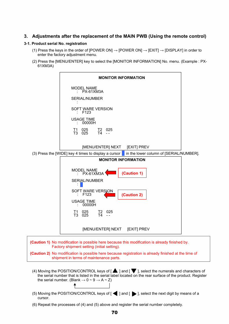
3. Adjustments after the replacement of the MAIN PWB (Using the remote control) 3-1. Product serial No. registration
(1) Press the keys in the order of [POWER ON] → [POWER ON] → [EXIT] → [DISPLAY] in order to enter the factory adjustment menu.
(2) Press the [MENU/ENTER] key to select the [MONITOR INFORMATION] No. menu. (Example : PX-61XM3A)
(3) Press the [WIDE] key 4 times to display a cursor in the lower column of [SERIAL/NUMBER].
(4) Moving the POSITION/CONTROL keys of [ ] and [ ], select the numerals and characters of
the serial number that is listed in the serial label located on the rear surface of the product. Register the serial number. (Blank → 0 ~ 9 → A ~ Z)
(5) Moving the POSITION/CONTROL keys of [ ] and [ ], select the next digit by means of a cursor.
(6) Repeat the processes of (4) and (5) above and register the serial number completely.
(Caution 1) No modification is possible here because this modification is already finished by. Factory shipment setting (initial setting).
(Caution 2) No modification is possible here because registration is already finished at the time of shipment in terms of maintenance parts.
MONITOR INFORMATION
MODEL NAME : PX-61XM3A
SERIAL/NUMBER : SOFT WARE VERSION : F123 USAGE TIME : 00000H T1 025 T2 025
T3 025 T4 - - [MENU/ENTER] NEXT [EXIT] PREV
MONITOR INFORMATION
MODEL NAME : PX-61XM3A
SERIAL/NUMBER : SOFT WARE VERSION : F123 USAGE TIME : 00000H T1 025 T2 025
T3 025 T4 - - [MENU/ENTER] NEXT [EXIT] PREV
(Caution 1)
(Caution 2)
70
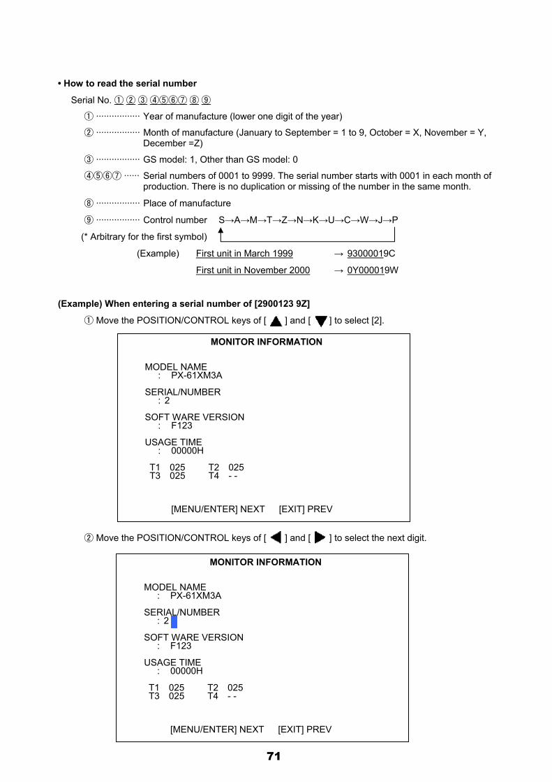
• How to read the serial number
Serial No.
················· Year of manufacture (lower one digit of the year)
················· Month of manufacture (January to September = 1 to 9, October = X, November = Y, December =Z)
················· GS model: 1, Other than GS model: 0
······ Serial numbers of 0001 to 9999. The serial number starts with 0001 in each month of production. There is no duplication or missing of the number in the same month.
················· Place of manufacture
················· Control number S→A→M→T→Z→N→K→U→C→W→J→P
(* Arbitrary for the first symbol)
(Example) First unit in March 1999 → 93000019C
First unit in November 2000 → 0Y000019W
(Example) When entering a serial number of [2900123 9Z]
Move the POSITION/CONTROL keys of [ ] and [ ] to select [2].
Move the POSITION/CONTROL keys of [ ] and [ ] to select the next digit.
MONITOR INFORMATION
MODEL NAME : PX-61XM3A
SERIAL/NUMBER : 2 SOFT WARE VERSION : F123 USAGE TIME : 00000H T1 025 T2 025
T3 025 T4 - - [MENU/ENTER] NEXT [EXIT] PREV
MONITOR INFORMATION
MODEL NAME : PX-61XM3A
SERIAL/NUMBER : 2 SOFT WARE VERSION : F123 USAGE TIME : 00000H T1 025 T2 025
T3 025 T4 - - [MENU/ENTER] NEXT [EXIT] PREV
71
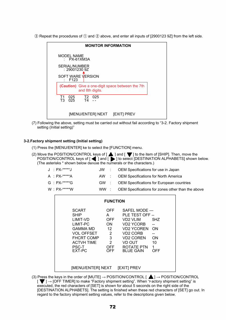
Repeat the procedures of and above, and enter all inputs of [2900123 9Z] from the left side.
(7) Following the above, setting must be carried out without fail according to “3-2. Factory shipment setting (Initial setting)”
3-2.Factory shipment setting (Initial setting)
(1) Press the [MENU/ENTER] ke to select the [FUNCTION] menu.
(2) Move the POSITION/CONTROL keys of [ ] and [ ] to the item of [SHIP]. Then, move the POSITION/CONTROL keys of [ ] and [ ] to select [DESTINATION ALPHABETS] shown below. (The asterisks * shown below denote the numerals or the characters.)
J : PX-*****J JW : OEM Specifications for use in Japan
A : PX-*****A AW : OEM Specifications for North America
G : PX-*****G GW : OEM Specifications for European countries
W : PX-*****W WW : OEM Specifications for zones other than the above
(3) Press the keys in the order of [MUTE] → POSITION/CONTROL [ ] → POSITION/CONTROL
[ ] → [OFF TIMER] to make “Factory shipment setting”. When “Factory shipment setting” is executed, the red characters of [SET] is shown for about 5 seconds on the right side of the [DESTINATION ALPHABETS]. The setting is finished when these red characters of [SET] go out. In regard to the factory shipment setting values, refer to the descriptions given below.
FUNCTION
SCART OFF SAFEL MODE --- SHIP A PLE TEST OFF -- LIMIT-VD OFF VD2 VLIM 5HZ LIMIT-PC ON VD2 YCORB -- GAMMA MD 12 VD2 YCOREN ON VOL OFFSET 2 VD2 CORB -- FHCRT COMP 3 VD2 COREN ON ACTVH TIME 2 VD OUT 10 PSC-T OFF ROTATE PTN 1 EXT-PC OFF BLUE GAIN OFF
[MENU/ENTER] NEXT [EXIT] PREV
MONITOR INFORMATION
MODEL NAME : PX-61XM3A
SERIAL/NUMBER : 29001230 9Z SOFT WARE VERSION : F123 USAGE TIME : 00000H T1 025 T2 025
T3 025 T4 - - [MENU/ENTER] NEXT [EXIT] PREV
(Caution) Give a one-digit space between the 7th and 8th digits.
72
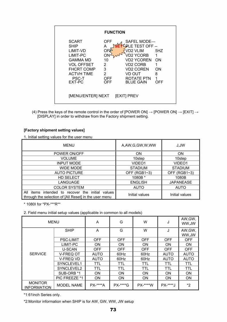
(4) Press the keys of the remote control in the order of [POWER ON] → [POWER ON] → [EXIT] →
[DISPLAY] in order to withdraw from the Factory shipment setting.
[Factory shipment setting values]
1. Initial setting values for the user menu
MENU A,AW,G,GW,W,WW J,JW
POWER ON/OFF ON ON VOLUME 10step 10step
INPUT MODE VIDEO1 VIDEO1 WIDE MODE STADIUM STADIUM
AUTO PICTURE OFF (RGB1~3) OFF (RGB1~3) HD SELECT 1080B * 1080B LANGUAGE ENGLISH JAPANEASE
COLOR SYSTEM AUTO AUTO All items intended to recover the initial values through the selection of [All Reset] in the user menu Initial values Initial values
* 1080I for *PX-***R**
2. Field menu initial setup values (applicable in common to all models)
MENU A G W J AW,GW,WW,JW
SHIP A G W J AW,GW,WW,JW
PSC-LIMIT OFF OFF OFF OFF OFF LIMIT-PC ON ON ON ON ON U-SCAN OFF OFF OFF OFF OFF
V-FREQ OT AUTO 60Hz 60Hz AUTO AUTO V-FREQ VD AUTO 60Hz 60Hz AUTO AUTO
SYNCLEVEL1 TTL TTL TTL TTL TTL SYNCLEVEL2 TTL TTL TTL TTL TTL SUB-ORB *1 ON ON ON ON ON
SERVICE
PIC FREEZE *1 ON ON ON ON ON MONITOR
INFORMATION MODEL NAME PX-****A PX-****G PX-****W PX-****J *2
*1:61inch Series only.
*2:Monitor information when SHIP is for AW, GW, WW, JW setup
FUNCTION
SCART OFF SAFEL MODE--- SHIP A SET PLE TEST OFF -- LIMIT-VD OFF VD2 VLIM 5HZ LIMIT-PC ON VD2 YCORB 1 GAMMA MD 10 VD2 YCOREN ON VOL OFFSET 2 VD2 CORB 1 FHCRT COMP 3 VD2 COREN ON ACTVH TIME 2 VD OUT 8
PSC-T OFF ROTATE PTN 1 EXT-PC OFF BLUE GAIN OFF [MENU/ENTER] NEXT [EXIT] PREV
73
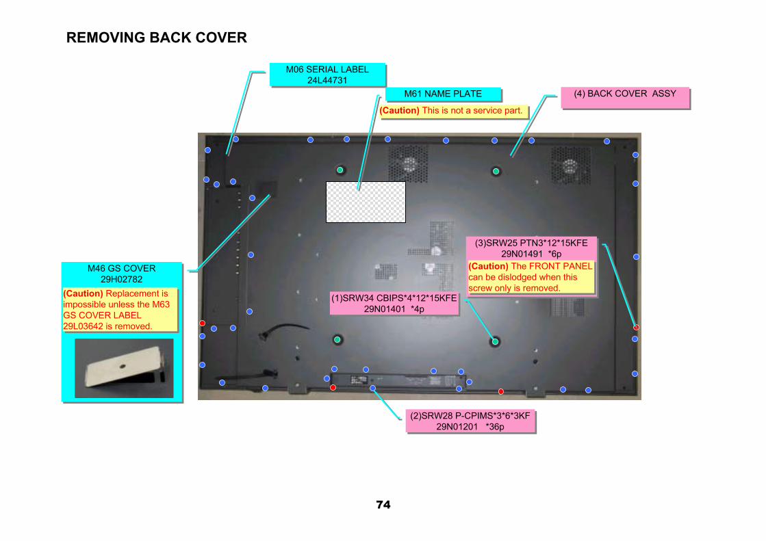
REMOVING BACK COVER
(4) BACK COVER ASSY(4) BACK COVER ASSY
(2)SRW28 P-CPIMS*3*6*3KF 29N01201 *36p
(2)SRW28 P-CPIMS*3*6*3KF 29N01201 *36p
M06 SERIAL LABEL24L44731
M06 SERIAL LABEL24L44731
(1)SRW34 CBIPS*4*12*15KFE 29N01401 *4p
(1)SRW34 CBIPS*4*12*15KFE 29N01401 *4p
M61 NAME PLATEM61 NAME PLATE
(3)SRW25 PTN3*12*15KFE 29N01491 *6p
(3)SRW25 PTN3*12*15KFE 29N01491 *6p
M46 GS COVER29H02782
M46 GS COVER29H02782
(Caution) This is not a service part.(Caution) This is not a service part.
(Caution) The FRONT PANEL can be dislodged when this screw only is removed.
(Caution) The FRONT PANEL can be dislodged when this screw only is removed.
(Caution) Replacement is impossible unless the M63 GS COVER LABEL 29L03642 is removed.
(Caution) Replacement is impossible unless the M63 GS COVER LABEL 29L03642 is removed.
74
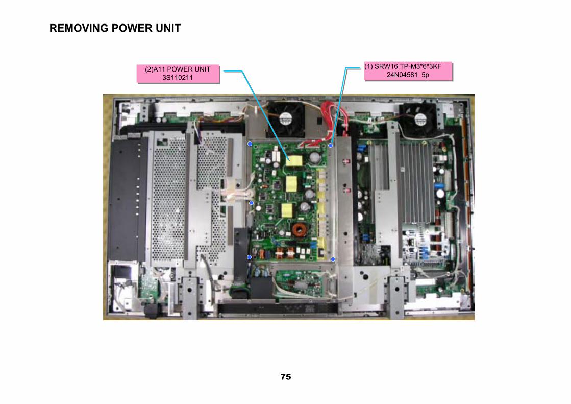
REMOVING POWER UNIT
(1) SRW16 TP-M3*6*3KF24N04581 5p
(1) SRW16 TP-M3*6*3KF24N04581 5p(2)A11 POWER UNIT
3S110211(2)A11 POWER UNIT
3S110211
75
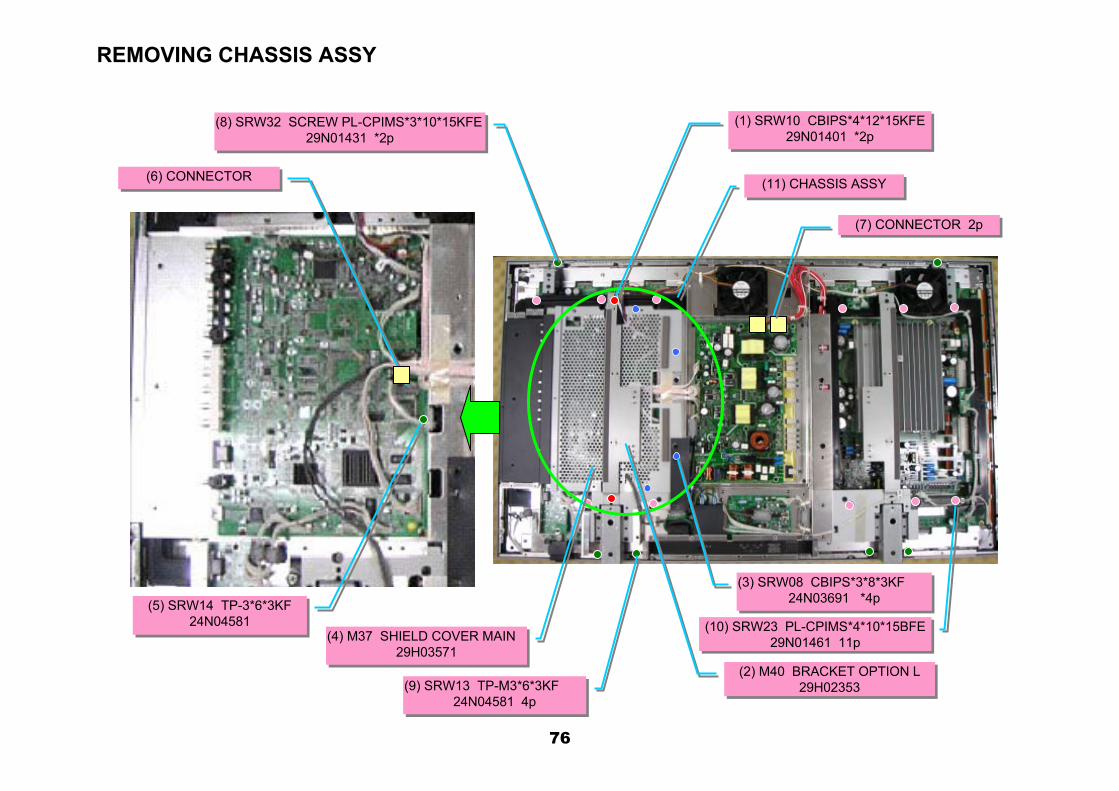
REMOVING CHASSIS ASSY
(2) M40 BRACKET OPTION L29H02353
(2) M40 BRACKET OPTION L29H02353
(1) SRW10 CBIPS*4*12*15KFE29N01401 *2p
(1) SRW10 CBIPS*4*12*15KFE29N01401 *2p
(6) CONNECTOR(6) CONNECTOR
(5) SRW14 TP-3*6*3KF24N04581
(5) SRW14 TP-3*6*3KF24N04581
(7) CONNECTOR 2p(7) CONNECTOR 2p
(10) SRW23 PL-CPIMS*4*10*15BFE29N01461 11p
(10) SRW23 PL-CPIMS*4*10*15BFE29N01461 11p
(11) CHASSIS ASSY(11) CHASSIS ASSY
(9) SRW13 TP-M3*6*3KF24N04581 4p
(9) SRW13 TP-M3*6*3KF24N04581 4p
(8) SRW32 SCREW PL-CPIMS*3*10*15KFE29N01431 *2p
(8) SRW32 SCREW PL-CPIMS*3*10*15KFE29N01431 *2p
(3) SRW08 CBIPS*3*8*3KF24N03691 *4p
(3) SRW08 CBIPS*3*8*3KF24N03691 *4p
(4) M37 SHIELD COVER MAIN29H03571
(4) M37 SHIELD COVER MAIN29H03571
76
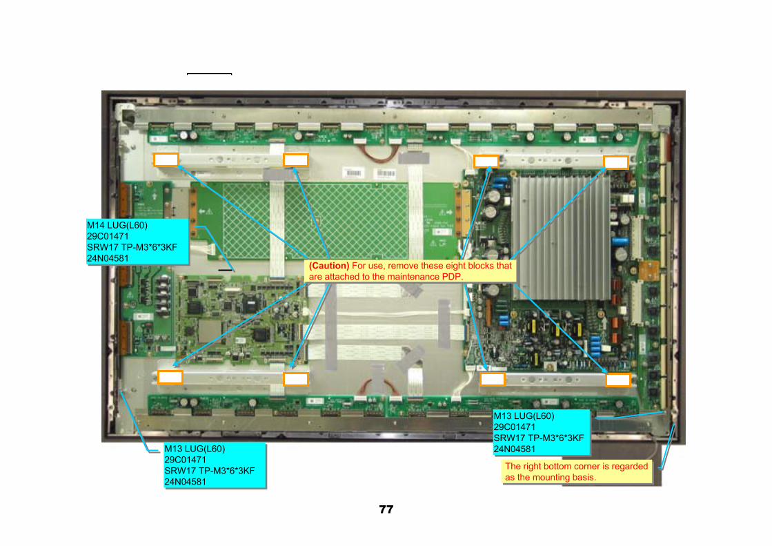
The right bottom corner is regarded as the mounting basis.The right bottom corner is regarded as the mounting basis.
M13 LUG(L60) 29C01471 SRW17 TP-M3*6*3KF24N04581
M13 LUG(L60) 29C01471 SRW17 TP-M3*6*3KF24N04581 M13 LUG(L60)
29C01471 SRW17 TP-M3*6*3KF24N04581
M13 LUG(L60) 29C01471 SRW17 TP-M3*6*3KF24N04581
M14 LUG(L60) 29C01471 SRW17 TP-M3*6*3KF24N04581
M14 LUG(L60) 29C01471 SRW17 TP-M3*6*3KF24N04581
(Caution) For use, remove these eight blocks that are attached to the maintenance PDP.(Caution) For use, remove these eight blocks that are attached to the maintenance PDP.
77

PDP-424MV
No signal With signal
PN 1 D+3.3 0 3.3 3.3 0 0 0 - POWER→MAIN2 D+3.3 0 3.3 3.3 0 0 0 - POWER→MAIN3 D+3.3 0 3.3 3.3 0 0 0 - POWER→MAIN4 D.GND GND 0 0 0 0 0 0 - -5 D.GND GND 0 0 0 0 0 0 - -6 D.GND GND 0 0 0 0 0 0 - -7 D+2.5 0 2.5 2.5 0 0 0 - POWER→MAIN8 D+2.5 0 2.5 2.5 0 0 0 - POWER→MAIN9 D+2.5 0 2.5 2.5 0 0 0 - POWER→MAIN
10 D.GND GND 0 0 0 0 0 0 - -11 D.GND GND 0 0 0 0 0 0 - -12 D.GND GND 0 0 0 0 0 0 - -
PM 1 M+7 6.8 6.8 6.8 6.8 6.8 6.8 - POWER→MAIN2 D.GND GND 0 0 0 0 0 0 - -3 POWER Power control 0 4.9 4.9 0 0 0 - MAIN→POWER4 D.GND GND 0 0 0 0 0 0 - -5 POMUTE Mute signal for AC power OFF 4.8 4.8 4.8 4.8 4.8 4.8 4.8→- POWER→MAIN6 SW7 Power start control 0 6.8 6.8 6.8 6.8 0 - POWER→MAIN7 NC Non-connection terminal - - - - - - - -
PV 1 A+12 12V power supply for analog circuits 0 12 12 0 0 0 - POWER→MAIN2 A.GND GND 0 0 0 0 0 0 - -3 A+6 6V power supply for analog circuits 0 6 6 0 0 0 - POWER→MAIN4 A+6 6V power supply for analog circuits 0 6 6 0 0 0 - POWER→MAIN5 A.GND GND 0 0 0 0 0 0 - -6 A.GND GND 0 0 0 0 0 0 - -7 NC Non-connection terminal - - - - - - - -8 NC Non-connection terminal - - - - - - - -
AU 1 AU_L Audio signal LCH
0 Selected inputsignals areoutput.
Selected inputsignals areoutput.
0 0 0 - MAIN→AUDIO
2 GND GND 0 0 0 0 0 0 - -3 AU_R Audio signal R
CH0 Selected input
signals areoutput.
Selected inputsignals areoutput.
0 0 0 - MAIN→AUDIO
4 GND GND 0 0 0 0 0 0 - -5 MUTE Mute signal of audio output 3.5 3.5→0 3.5→0 3.5 3.5→0 3.5 3.5→- MAIN→AUDIO6 SCL7 Clock line of the I2C bus 0 Clock signal
(5Vac) whendata arereceived; 5Vdcwhen no dataare received.
Clock signal(5Vac) whendata arereceived; 5Vdcwhen no dataare received.
0 0 0 - MAIN→AUDIO
7 SDA7 Data line of the I2C bus 0 Clock signal(5Vac) whendata arereceived; 5Vdcwhen no dataare received.
Clock signal(5Vac) whendata arereceived; 5Vdcwhen no dataare received.
1 1 0 - MAIN→AUDIO
RS 1 M+5V 5V power supply for microcomputer 0 5 5 5 5 0 - MAIN→RS232C2 TXD RS232 driver output 0 Clock signal
used duringdatatransmission(3.3Vac)3.3Vdc whenno data arereceived.
Clock signalused duringdatatransmission(3.3Vac)3.3Vdc whenno data arereceived.
Clock signalused duringdatatransmission(3.3Vac)3.3Vdc whenno data arereceived.
Clock signalused duringdatatransmission(3.3Vac)3.3Vdc whenno data arereceived.
0
-
MAIN→RS232C
3 GND GND 0 0 0 0 0 0 - -4 RXD RS232 receiver input 0 Clock signal
(3.3Vac) whendata arereceived;3.3Vdc whenno data arereceived.
Clock signal(3.3Vac) whendata arereceived;3.3Vdc whenno data arereceived.
Clock signal(3.3Vac) whendata arereceived;3.3Vdc whenno data arereceived.
Clock signal(3.3Vac) whendata arereceived;3.3Vdc whenno data arereceived.
0 - RS232C→MAIN
5 M+3.3V 3.3V power supply for microcomputer 0 3.3 3.3 3.3 3.3 0 - MAIN→RS232C6 GND GND 0 0 0 0 0 0 - -7 REMIN2/RXD
1Data signal ofwired remotecontrol
42VM542VP542XM350XM461XM3
0 Clock signal(3.3Vac) whendata arereceived;3.3Vdc whenno data arereceived.
Clock signal(3.3Vac) whendata arereceived;3.3Vdc whenno data arereceived.
Clock signal(3.3Vac) whendata arereceived;3.3Vdc whenno data arereceived.
Clock signal(3.3Vac) whendata arereceived;3.3Vdc whenno data arereceived.
0 - RS232C→MAIN
42VR542XR350XR461XR3
0 0 0 0 0 0 -
8 RESET SW NC - - - - - - - -9 PLE_CTL PLE control 42VM5
42VP542XM350XM461XM3
0 3.3V duningdatatransmissionfor VideoWOLL0V when nodata aretransmitted
3.3V duningdatatransmissionfor VideoWOLL0V when nodata aretransmitted
3.3V duningdatatransmissionfor VideoWOLL0V when nodata aretransmitted
0 0 - MAIN→RS232C
42VR542XR350XR461XR3
0 0 0 0 0 0 -
10 TXD1 RS232 driveroutput
42VM542VP542XM350XM461XM3
0 Clock signalused duringdatatransmission(5Vac) 5Vdcwhen no dataaretransmitted.
Clock signalused duringdatatransmission(5Vac) 5Vdcwhen no dataaretransmitted.
Clock signalused duringdatatransmission(5Vac) 5Vdcwhen no dataaretransmitted.
0 0 - MAIN→RS232C
2.5V power supply for digital circuits
2.5V power supply for digital circuits
7V power supply for microcomputer
Signal direction
Main power ON (POWER button ON)
Pin No. Pin name Function Standby
Powermanagement
2.5V power supply for digital circuits
Main powerOFF
(Caution) The operating voltages specified below are used in common irrespective of the presence of signals. In this case, however, part of the operating voltages (red characters) may change accordingto the signal conditions when the main power supply is turned on (POWER button ON).Status of LED lighting: for lighting in green, for unlighting, and for lighting in red. Vol.1
3.3V power supply for digital circuits3.3V power supply for digital circuits3.3V power supply for digital circuits
AC power OFF(Power cordpulled out of
the wall outlet)
AC power ON(Power cordconnected to
the wall outlet)
Basic operation (Numerical unit: Vdc; except for the case when units are individually indicated)
Name
78
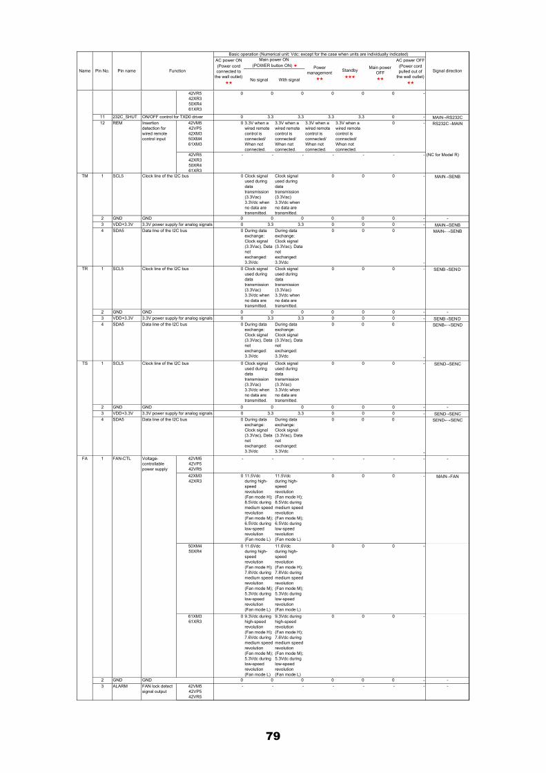
No signal With signal
Signal direction
Main power ON (POWER button ON)
Pin No. Pin name Function Standby
Powermanagement
Main powerOFF
AC power OFF(Power cordpulled out of
the wall outlet)
AC power ON(Power cordconnected to
the wall outlet)
Basic operation (Numerical unit: Vdc; except for the case when units are individually indicated)
Name
42VR542XR350XR461XR3
0 0 0 0 0 0 -
11 232C_SHUT ON/OFF control for TXD0 driver 0 3.3 3.3 3.3 3.3 0 - MAIN→RS232C12 REM Insertion
detection forwired remotecontrol input
42VM542VP542XM350XM461XM3
0 3.3V when awired remotecontrol isconnected/When notconnected.
3.3V when awired remotecontrol isconnected/When notconnected.
3.3V when awired remotecontrol isconnected/When notconnected.
3.3V when awired remotecontrol isconnected/When notconnected.
0 - RS232C→MAIN
42VR542XR350XR461XR3
- - - - - - - (NC for Model R)
TM 1 SCL5 Clock line of the I2C bus 0 Clock signalused duringdatatransmission(3.3Vac)3.3Vdc whenno data aretransmitted.
Clock signalused duringdatatransmission(3.3Vac)3.3Vdc whenno data aretransmitted.
0 0 0 - MAIN→SENB
2 GND GND 0 0 0 0 0 0 - -3 VDD+3.3V 3.3V power supply for analog signals 0 3.3 3.3 0 0 0 - MAIN→SENB4 SDA5 Data line of the I2C bus 0 During data
exchange:Clock signal(3.3Vac), Datanotexchanged:3.3Vdc
During dataexchange:Clock signal(3.3Vac), Datanotexchanged:3.3Vdc
0 0 0
-
MAIN←→SENB
TR 1 SCL5 Clock line of the I2C bus 0 Clock signalused duringdatatransmission(3.3Vac)3.3Vdc whenno data aretransmitted.
Clock signalused duringdatatransmission(3.3Vac)3.3Vdc whenno data aretransmitted.
0 0 0 - SENB→SEND
2 GND GND 0 0 0 0 0 0 - -3 VDD+3.3V 3.3V power supply for analog signals 0 3.3 3.3 0 0 0 - SENB→SEND4 SDA5 Data line of the I2C bus 0 During data
exchange:Clock signal(3.3Vac), Datanotexchanged:3.3Vdc
During dataexchange:Clock signal(3.3Vac), Datanotexchanged:3.3Vdc
0 0 0
-
SENB←→SEND
TS 1 SCL5 Clock line of the I2C bus 0 Clock signalused duringdatatransmission(3.3Vac)3.3Vdc whenno data aretransmitted.
Clock signalused duringdatatransmission(3.3Vac)3.3Vdc whenno data aretransmitted.
0 0 0 - SEND→SENC
2 GND GND 0 0 0 0 0 0 - -3 VDD+3.3V 3.3V power supply for analog signals 0 3.3 3.3 0 0 0 - SEND→SENC4 SDA5 Data line of the I2C bus 0 During data
exchange:Clock signal(3.3Vac), Datanotexchanged:3.3Vdc
During dataexchange:Clock signal(3.3Vac), Datanotexchanged:3.3Vdc
0 0 0
-
SEND←→SENC
FA 1 FAN-CTL Voltage-controllablepower supply
42VM542VP542VR5
- - - - - - - -
42XM342XR3
0 11.5Vdcduring high-speedrevolution(Fan mode H);8.5Vdc duringmedium speedrevolution(Fan mode M);6.5Vdc duringlow-speedrevolution(Fan mode L)
11.5Vdcduring high-speedrevolution(Fan mode H);8.5Vdc duringmedium speedrevolution(Fan mode M);6.5Vdc duringlow-speedrevolution(Fan mode L)
0 0 0 - MAIN→FAN
50XM450XR4
0 11.6Vdcduring high-speedrevolution(Fan mode H);7.8Vdc duringmedium speedrevolution(Fan mode M);5.3Vdc duringlow-speedrevolution(Fan mode L)
11.6Vdcduring high-speedrevolution(Fan mode H);7.8Vdc duringmedium speedrevolution(Fan mode M);5.3Vdc duringlow-speedrevolution(Fan mode L)
0 0 0 -
61XM361XR3
0 9.3Vdc duringhigh-speedrevolution(Fan mode H);7.6Vdc duringmedium speedrevolution(Fan mode M);5.3Vdc duringlow-speedrevolution(Fan mode L)
9.3Vdc duringhigh-speedrevolution(Fan mode H);7.6Vdc duringmedium speedrevolution(Fan mode M);5.3Vdc duringlow-speedrevolution(Fan mode L)
0 0 0 -
2 GND GND 0 0 0 0 0 0 - -3 ALARM 42VM5
42VP542VR5
- - - - - - - -FAN lock detectsignal output
79
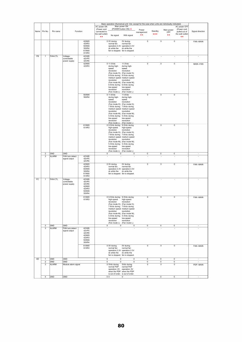
No signal With signal
Signal direction
Main power ON (POWER button ON)
Pin No. Pin name Function Standby
Powermanagement
Main powerOFF
AC power OFF(Power cordpulled out of
the wall outlet)
AC power ON(Power cordconnected to
the wall outlet)
Basic operation (Numerical unit: Vdc; except for the case when units are individually indicated)
Name
42XM342XR350XM450XR461XM361XR3
0 0V duringnormal fanoperation;3.3Vdc while thefan is stopped.
0V duringnormal fanoperation;3.3Vdc while thefan is stopped.
0 0 0 - FAN→MAIN
FB 1 FAN-CTL Voltage-controllablepower supply
42VM542VP542VR5
- - - - - - - -
42XM342XR3
0 11.5Vdcduring high-speedrevolution(Fan mode H);8.5Vdc duringmedium speedrevolution(Fan mode M);6.5Vdc duringlow-speedrevolution(Fan mode L)
11.5Vdcduring high-speedrevolution(Fan mode H);8.5Vdc duringmedium speedrevolution(Fan mode M);6.5Vdc duringlow-speedrevolution(Fan mode L)
0 0 0 - MAIN→FAN
50XM450XR4
0 11.6Vdcduring high-speedrevolution(Fan mode H);7.8Vdc duringmedium speedrevolution(Fan mode M);5.3Vdc duringlow-speedrevolution(Fan mode L)
11.6Vdcduring high-speedrevolution(Fan mode H);7.8Vdc duringmedium speedrevolution(Fan mode M);5.3Vdc duringlow-speedrevolution(Fan mode L)
0 0 0 -
61XM361XR3
0 9.3Vdc duringhigh-speedrevolution(Fan mode H);7.6Vdc duringmedium speedrevolution(Fan mode M);5.3Vdc duringlow-speedrevolution(Fan mode L)
9.3Vdc duringhigh-speedrevolution(Fan mode H);7.6Vdc duringmedium speedrevolution(Fan mode M);5.3Vdc duringlow-speedrevolution(Fan mode L)
0 0 0 -
2 GND GND 0 0 0 0 0 0 - -3 ALARM 42VM5
42VP542VR5
- - - - - - - -
42XM342XR350XM450XR461XM361XR3
0 0V duringnormal fanoperation;3.3Vdc while thefan is stopped.
0V duringnormal fanoperation;3.3Vdc while thefan is stopped.
0 0 0 - FAN→MAIN
FC 1 FAN-CTL Voltage-controllablepower supply
42VM542VP542VR542XM342XR350XM450XR4
- - - - - - - -
61XM361XR3
0 9.3Vdc duringhigh-speedrevolution(Fan mode H);7.6Vdc duringmedium speedrevolution(Fan mode M);5.3Vdc duringlow-speedrevolution(Fan mode L)
9.3Vdc duringhigh-speedrevolution(Fan mode H);7.6Vdc duringmedium speedrevolution(Fan mode M);5.3Vdc duringlow-speedrevolution(Fan mode L)
0 0 0 - FAN→MAIN
2 GND GND 0 0 0 0 0 0 - -3 ALARM 42VM5
42VP542VR542XM342XR350XM450XR4
- - - - - - - -
61XM361XR3
0 0V duringnormal fanoperation;3.3Vdc while thefan is stopped.
0V duringnormal fanoperation;3.3Vdc while thefan is stopped.
0 0 0 - FAN→MAIN
AD 1 GND GND 0 0 0 0 0 0 - -2 GND GND 0 0 0 0 0 0 - -3 ALARM Module alarm signal 0 5Vdc during
normal PDPoperation; 0Vwhen the PDPis out of order.
5Vdc duringnormal PDPoperation; 0Vwhen the PDPis out of order.
0 0 0 - PDP→MAIN
4 GND GND 0 0 0 0 0 0 - -
FAN lock detectsignal output
FAN lock detectsignal output
80
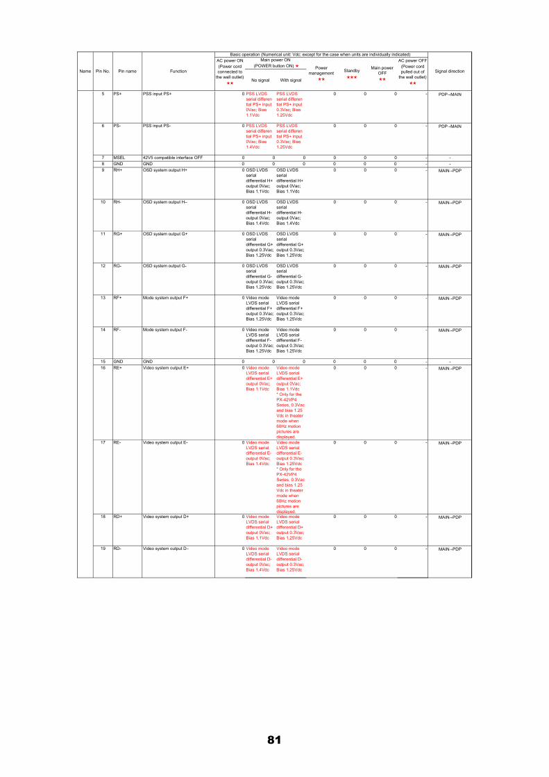
No signal With signal
Signal direction
Main power ON (POWER button ON)
Pin No. Pin name Function Standby
Powermanagement
Main powerOFF
AC power OFF(Power cordpulled out of
the wall outlet)
AC power ON(Power cordconnected to
the wall outlet)
Basic operation (Numerical unit: Vdc; except for the case when units are individually indicated)
Name
5 PS+ PSS input PS+ 0 PSS LVDSserial differential PS+ input0Vac; Bias1.1Vdc
PSS LVDSserial differential PS+ input0.3Vac; Bias1.25Vdc
0 0 0 - PDP→MAIN
6 PS- PSS input PS- 0 PSS LVDSserial differential PS+ input0Vac; Bias1.4Vdc
PSS LVDSserial differential PS+ input0.3Vac; Bias1.25Vdc
0 0 0 - PDP→MAIN
7 MSEL 42V5 compatible interface OFF 0 0 0 0 0 0 - -8 GND GND 0 0 0 0 0 0 - -9 RH+ OSD system output H+ 0 OSD LVDS
serialdifferential H+output 0Vac;Bias 1.1Vdc
OSD LVDSserialdifferential H+output 0Vac;Bias 1.1Vdc
0 0 0 - MAIN→PDP
10 RH- OSD system output H– 0 OSD LVDSserialdifferential H-output 0Vac;Bias 1.4Vdc
OSD LVDSserialdifferential H-output 0Vac;Bias 1.4Vdc
0 0 0 - MAIN→PDP
11 RG+ OSD system output G+ 0 OSD LVDSserialdifferential G+output 0.3Vac;Bias 1.25Vdc
OSD LVDSserialdifferential G+output 0.3Vac;Bias 1.25Vdc
0 0 0 - MAIN→PDP
12 RG- OSD system output G- 0 OSD LVDSserialdifferential G-output 0.3Vac;Bias 1.25Vdc
OSD LVDSserialdifferential G-output 0.3Vac;Bias 1.25Vdc
0 0 0 - MAIN→PDP
13 RF+ Mode system output F+ 0 Video modeLVDS serialdifferential F+output 0.3Vac;Bias 1.25Vdc
Video modeLVDS serialdifferential F+output 0.3Vac;Bias 1.25Vdc
0 0 0 - MAIN→PDP
14 RF- Mode system output F- 0 Video modeLVDS serialdifferential F-output 0.3Vac;Bias 1.25Vdc
Video modeLVDS serialdifferential F-output 0.3Vac;Bias 1.25Vdc
0 0 0 - MAIN→PDP
15 GND GND 0 0 0 0 0 0 - -16 RE+ Video system output E+ 0 Video mode
LVDS serialdifferential E+output 0Vac;Bias 1.1Vdc
Video modeLVDS serialdifferential E+output 0Vac;Bias 1.1Vdc* Only for thePX-42VP4Series, 0.3Vacand bias 1.25Vdc in theatermode when60Hz motionpictures aredisplayed.
0 0 0 - MAIN→PDP
17 RE- Video system output E- 0 Video modeLVDS serialdifferential E-output 0Vac;Bias 1.4Vdc
Video modeLVDS serialdifferential E-output 0.3Vac;Bias 1.25Vdc* Only for thePX-42VP4Series, 0.3Vacand bias 1.25Vdc in theatermode when60Hz motionpictures aredisplayed.
0 0 0 - MAIN→PDP
18 RD+ Video system output D+ 0 Video modeLVDS serialdifferential D+output 0Vac;Bias 1.1Vdc
Video modeLVDS serialdifferential D+output 0.3Vac;Bias 1.25Vdc
0 0 0 - MAIN→PDP
19 RD- Video system output D– 0 Video modeLVDS serialdifferential D-output 0Vac;Bias 1.4Vdc
Video modeLVDS serialdifferential D-output 0.3Vac;Bias 1.25Vdc
0 0 0 - MAIN→PDP
81
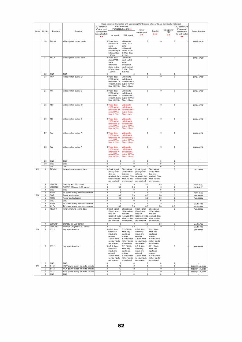
No signal With signal
Signal direction
Main power ON (POWER button ON)
Pin No. Pin name Function Standby
Powermanagement
Main powerOFF
AC power OFF(Power cordpulled out of
the wall outlet)
AC power ON(Power cordconnected to
the wall outlet)
Basic operation (Numerical unit: Vdc; except for the case when units are individually indicated)
Name
20 RCLK+ Video system output clock+ 0 Video dataclock LVDSserialdifferentialclock+ output0.3Vac; Bias1.25Vdc
Video dataclock LVDSserialdifferentialclock+ output0.3Vac; Bias1.25Vdc
0 0 0 - MAIN→PDP
21 RCLK- Video system output clock– 0 Video dataclock LVDSserialdifferentialclock- output0.3Vac; Bias1.25Vdc
Video dataclock LVDSserialdifferentialclock- output0.3Vac; Bias1.25Vdc
0 0 0 - MAIN→PDP
22 GND GND 0 0 0 0 0 0 - -23 RC+ Video system output C+ 0 Video data
LVDS serialdifferential C+output 0.3Vac;Bias 1.25Vdc
Video dataLVDS serialdifferential C+output 0.3Vac;Bias 1.25Vdc
0 0 0 - MAIN→PDP
24 RC- Video system output C– 0 Video dataLVDS serialdifferential C-output 0.3Vac;Bias 1.25Vdc
Video dataLVDS serialdifferential C-output 0.3Vac;Bias 1.25Vdc
0 0 0 - MAIN→PDP
25 RB+ Video system output B+ 0 Video dataLVDS serialdifferential B+output 0Vac;Bias 1.1Vdc
Video dataLVDS serialdifferential B+output 0Vac;Bias 1.1Vdc
0 0 0 - MAIN→PDP
26 RB- Video system output B– 0 Video dataLVDS serialdifferential B-output 0Vac;Bias 1.4Vdc
Video dataLVDS serialdifferential B-output 0.3Vac;Bias 1.25Vdc
0 0 0 - MAIN→PDP
27 RA+ Video system output A+ 0 Video dataLVDS serialdifferential A+output 0Vac;Bias 1.1Vdc
Video dataLVDS serialdifferential A+output 0.3Vac;Bias 1.25Vdc
0 0 0 - MAIN→PDP
28 RA- Video system output A– 0 Video dataLVDS serialdifferential A-output 0Vac;Bias 1.4Vdc
Video dataLVDS serialdifferential A-output 0.3Vac;Bias 1.25Vdc
0 0 0 - MAIN→PDP
29 GND GND 0 0 0 0 0 0 - -30 GND GND 0 0 0 0 0 0 - -31 GND GND 0 0 0 0 0 0 - -
LD 1 REMIN1 Infrared remote control data 0 Clock signal(5Vac) whendata arereceived; 5Vdcwhen no dataare received.
Clock signal(5Vac) whendata arereceived; 5Vdcwhen no dataare received.
Clock signal(5Vac) whendata arereceived; 5Vdcwhen no dataare received.
Clock signal(5Vac) whendata arereceived; 5Vdcwhen no dataare received.
0
-
LED→PWR
2 LEDCTL1 Standby red LED control 0 0 0 3.3 3.3 0 - PWR→LED3 LEDCTL2 POWER ON green LED control 0 3.3 3.3 0 0 0 - PWR→LED4 GND GND 0 0 0 0 0 0 - -5 M+5V 5V power supply for microcomputer 0 5 5 5 5 0 - PWR→LED
PW 1 SW7 Power start control 0 6.8 6.8 6.8 6.8 0 - PW→MAIN2 POIN Power start detection 0 3.3 3.3 3.3 3.3 0 - PW→MAIN3 GND GND 0 0 0 0 0 0 - -4 M+5V 5V power supply for microcomputer 0 5 5 5 5 0 - MAIN→PW5 M+7V 7V power supply for microcomputer 0 6.8 6.8 6.8 6.8 6.8 - MAIN→PW6 REMIN1 Infrared remote control data 0 Clock signal
(5Vac) whendata arereceived; 5Vdcwhen no dataare received.
Clock signal(5Vac) whendata arereceived; 5Vdcwhen no dataare received.
Clock signal(5Vac) whendata arereceived; 5Vdcwhen no dataare received.
Clock signal(5Vac) whendata arereceived; 5Vdcwhen no dataare received.
0 - PW→MAIN
7 LEDCTL1 Standby red LED control 0 0 0 3.3 3.3 0 - MAIN→PW8 LEDCTL2 POWER ON green LED control 0 3.3 3.3 0 0 0 - MAIN→PW
SW 1 CTL1 Key input detection 0 0.7~2.8Vdcwhen keyinputs areentered;3.3Vdc whenno key inputsare entered.
0.7~2.8Vdcwhen keyinputs areentered;3.3Vdc whenno key inputsare entered.
0.7~2.8Vdcwhen keyinputs areentered;3.3Vdc whenno key inputsare entered.
0.7~2.8Vdcwhen keyinputs areentered;3.3Vdc whenno key inputsare entered.
0 - SW→MAIN
2 CTL2 Key input detection 0 0.7~2.8Vdcwhen keyinputs areentered;3.3Vdc whenno key inputsare entered.
0.7~2.8Vdcwhen keyinputs areentered;3.3Vdc whenno key inputsare entered.
0.7~2.8Vdcwhen keyinputs areentered;3.3Vdc whenno key inputsare entered.
0.7~2.8Vdcwhen keyinputs areentered;3.3Vdc whenno key inputsare entered.
0 - SW→MAIN
3 GND GND 0 0 0 0 0 0 - -PA 1 S+12 +12V power supply for audio circuits 0 12 12 0 0 0 - POWER→AUDIO
2 S+12 +12V power supply for audio circuits 0 12 12 0 0 0 - POWER→AUDIO3 S+12 +12V power supply for audio circuits 0 12 12 0 0 0 - POWER→AUDIO4 GND GND 0 0 0 0 0 0 - -
82

No signal With signal
Signal direction
Main power ON (POWER button ON)
Pin No. Pin name Function Standby
Powermanagement
Main powerOFF
AC power OFF(Power cordpulled out of
the wall outlet)
AC power ON(Power cordconnected to
the wall outlet)
Basic operation (Numerical unit: Vdc; except for the case when units are individually indicated)
Name
5 GND GND 0 0 0 0 0 0 - -6 GND GND 0 0 0 0 0 0 - -
PD 1 ALARM PDP alarm signal 0 5Vdc when thePDP is normal;0V when it isabnormal.
5Vdc when thePDP is normal;0V when it isabnormal.
0 0 0 - PDP→POWER
2 D.GND GND 0 0 0 0 0 0 - -3 D.GND GND 0 0 0 0 0 0 - -4 D.GND GND 0 0 0 0 0 0 - -5 D.GND GND 0 0 0 0 0 0 - -6 D+60 Vd power supply
for PDP0 60Vdc
(changeableaccording tothe PDP)
60Vdc(changeableaccording tothe PDP)
0 0 0 - PDWER→PDP
7 D+60 digital circuits 0 60Vdc(changeableaccording tothe PDP)
60Vdc(changeableaccording tothe PDP)
0 0 0 - PDWER→PDP
8 NC digital circuits - - - - - - - -9 D+170 Vs power supply
for PDP high-voltage circuits
0 170Vdc(changeableaccording tothe PDP)
170Vdc(changeableaccording tothe PDP)
0 0 0
-
PDWER→PDP
10 D+170 Vs power supplyfor PDP high-voltage circuits
0 170Vdc(changeableaccording tothe PDP)
170Vdc(changeableaccording tothe PDP)
0 0 0 - PDWER→PDP
1 ALARM PDP alarm signal 0 5Vdc when thePDP is normal;0V when it isabnormal.
5Vdc when thePDP is normal;0V when it isabnormal.
0 0 0 - PDP→POWER
2 D.GND GND 0 0 0 0 0 0 - -3 D.GND GND 0 0 0 0 0 0 - -4 D+5 5V power supply
for digital circuits0 5.15 5.15 0 0 0
-POWER→PDP
5 D.GND GND 0 0 0 0 0 0 - -6 D.GND GND 0 0 0 0 0 0 - -7 D+65 Vd power supply
for PDP0 65Vdc
(changeableaccording tothe PDP)
65Vdc(changeableaccording tothe PDP)
0 0 0 - POWER→PDP
8 NC digital circuits - - - - - - - -9 D+175 Vs power supply
for PDP high-voltage circuits
0 175Vdc(changeableaccording tothe PDP)
175Vdc(changeableaccording tothe PDP)
0 0 0
-
POWER→PDP
10 D+175 Vs power supplyfor PDP high-voltage circuits
0 175Vdc(changeableaccording tothe PDP)
175Vdc(changeableaccording tothe PDP)
0 0 0 - POWER→PDP
PH 1 D+5 5V power supplyfor digital circuits
0 5.15 5.15 0 0 0-
PDWER→PDP
2 D+5 5V power supplyfor digital circuits
0 5.15 5.15 0 0 0-
PDWER→PDP
3 D.GND GND 0 0 0 0 0 0 - -4 D.GND GND 0 0 0 0 0 0
--
1 D+175 Vs power supplyfor PDP high-voltage circuits
0 175Vdc(changeableaccording tothe PDP)
175Vdc(changeableaccording tothe PDP)
0 0 0
-
POWER→PDP
2 D+175 Vs power supplyfor PDP high-voltage circuits
0 175Vdc(changeableaccording tothe PDP)
175Vdc(changeableaccording tothe PDP)
0 0 0
-
POWER→PDP
3 NC Non-connection - - - - - - - -4 D+65 Vd power supply
for PDP0 65Vdc
(changeableaccording tothe PDP)
65Vdc(changeableaccording tothe PDP)
0 0 0
-
POWER→PDP
5 D.GND digital circuits 0 0 0 0 0 0 - -6 D.GND GND 0 0 0 0 0 0 - -7 D+5 5V power supply
for digital circuits0 5.15 5.15 0 0 0
-POWER→PDP
8 D.GND GND 0 0 0 0 0 0 - -9 D.GND GND 0 0 0 0 0 0 - -
61XM361XR3
42VM542VP542VR542XM342XR350XM450XR4
61XM361XR3
42VM542VP542VR542XM342XR350XM450XR4
83