Embed Size (px)
Citation preview

1
SANDIA REPORT SAND2015-1071 Unlimited Release Printed February 2015
Final Report MEPV
Greg Nielson, Jeffrey Nelson, Murat Okandan, Vipin Gupta, Jos Luis Cruz-Campa, Tony Lentine, Bill Sweatt, Robert Biefeld, Keith Ortiz, Alyssa Christy, Scott Paap, Anna Tauke-Pedretti, Carlos Sanchez, Jeffrey Cederberg, Paul Resnick, Eric Langlois, Daniel Koleske, Jonathan Wierer, Willie Luk, Ben Anderson, Bradley Jared, Ron Goeke, Michael Hibbs, William Miller, David Zamora, Bob Chambers, Brenton Elisberg, Jason Wheeler, Dan Savignon, Brent Dial, Michael Haney (University of Delaware), Tian Gu (University of Delaware), and Gautam Agrawal (University of Delaware) Prepared by Sandia National Laboratories Albuquerque, New Mexico 87185 and Livermore, California 94550 Sandia National Laboratories is a multi-program laboratory managed and operated by Sandia Corporation, a wholly owned subsidiary of Lockheed Martin Corporation, for the U.S. Department of Energy's National Nuclear Security Administration under contract DE-AC04-94AL85000. Approved for public release; further dissemination unlimited.

2
Issued by Sandia National Laboratories, operated for the United States Department of Energy by Sandia Corporation.
NOTICE: This report was prepared as an account of work sponsored by an agency of the United States Government. Neither the United States Government, nor any agency thereof, nor any of their employees, nor any of their contractors, subcontractors, or their employees, make any warranty, express or implied, or assume any legal liability or responsibility for the accuracy, completeness, or usefulness of any information, apparatus, product, or process disclosed, or represent that its use would not infringe privately owned rights. Reference herein to any specific commercial product, process, or service by trade name, trademark, manufacturer, or otherwise, does not necessarily constitute or imply its endorsement, recommendation, or favoring by the United States Government, any agency thereof, or any of their contractors or subcontractors. The views and opinions expressed herein do not necessarily state or reflect those of the United States Government, any agency thereof, or any of their contractors.
Printed in the United States of America. This report has been reproduced directly from the best available copy.
Available to DOE and DOE contractors from
U.S. Department of Energy Office of Scientific and Technical Information P.O. Box 62 Oak Ridge, TN 37831
Telephone: (865) 576-8401 Facsimile: (865) 576-5728 E-Mail: [email protected] Online ordering: http://www.osti.gov/bridge
Available to the public from
U.S. Department of Commerce National Technical Information Service 5285 Port Royal Rd. Springfield, VA 22161
Telephone: (800) 553-6847 Facsimile: (703) 605-6900 E-Mail: [email protected] Online order: http://www.ntis.gov/help/ordermethods.asp?loc=7-4-0#online

3
SAND2015-1071 Unlimited Release
Printed February 2015
Final Report MEPV
Greg Nielson, Jeffrey Nelson, Murat Okandan, Vipin Gupta, Jos Luis Cruz-Campa, Tony Lentine, Bill Sweatt, Robert Biefeld, Keith Ortiz, Alyssa Christy, Scott Paap*, Anna Tauke-Pedretti, Carlos Sanchez, Jeffrey Cederberg, Paul Resnick, Eric Langlois, Daniel Koleske, Jonathan Wierer, Willie Luk, Ben Anderson, Bradley Jared, Ron Goeke, Michael Hibbs, William Miller, David Zamora, Bob Chambers, Brenton Elisberg, Jason Wheeler, Dan Savignon, and Brent Dial
Sandia National Laboratories P.O. Box 5800
Albuquerque, NM 87185
* P.O. Box 969 Livermore, CA 94551-0969
Michael Haney, Tian Gu, and Gautam Agrawal University of Delaware
Abstract
The MEPV Grand Challenge was focused on exploiting beneficial scaling effects in solar cells, modules, and systems to make solar power the lowest cost source of power available. The project explored new multi-junction, micro-scale solar cell architectures, new micro-optical concentration methods, new hybrid solar collection concepts, and developed a series of prototypes to demonstrate these technologies. In addition, a detailed cost analysis was conducted to determine the costs of the proposed technologies and provide guidance for the system design efforts. Key results included demonstration of InGaP/GaAS cells transferred to active silicon cells to create a three junction cell with efficiency near 30%, the transfer of InGaAs cells to Si with demonstrated high performance of the InGaAs cell behind the Si substrate, the design, manufacture, and experimental demonstration of optics with almost 90% transmission efficiency and 100X and 200X concentration with a relatively large acceptance angle (>±1.5°), and the full assembly and demonstration of functional micro-concentrator systems. The cost modeling efforts indicated that a module based on the best design resulting from the knowledge and technology develop would approach $1/Wpeak total installed system cost with no subsidies. If achieved in practice, this system would provide the lowest energy cost of any grid-tied energy source.

4
Acknowledgements
The project leaders gratefully acknowledge the many technical and programmatic contributions from Sandia Executive Management, the LDRD office, the dedicated technologist and students, business support professionals, and Perspectives, Inc. Sandia Executive Management: Julia Phillips Charles Barbour Gil Herrera Carol Adkins LDRD Office: Sheri Martinez Donna Chavez Tanci Wilson Business Support Professionals: Alex Andrego Adams Olivia Tsai Martin Finston Robert Westervelt Perspectives, Inc: Richard Macklin Marcia Pinzon Ann Miksovic Dedicated Technologists and Students: Sara Homeijer, Jaime McClain, Jennifer Barrios, Julie Chavez, Karen Cross, Gerald Girard, Janet Nguyen, Ian Luna, Sally Samora, Pablita Vigil, Travis Young, Mike Wiwi, David Torres, David Saiz, Michael Romero, Carl Smith, Jeramy Dickerson, Joanetta Ramos, Donald Bradley, David Calkins, Miriam Hilborn, Ann Trujillo, Billy Cunningham, Michael Denton, Jeffrey Kempisty, Michael Rye, Deanna Lopez, Kathleen Hines, Mathew Pohl, Steven Wolfley, Chistine Ford, Brandan Aguirre, Darrell Alliman, Charles Alford, and John Bower

5
Table of Contents
Abstract ......................................................................................................................................................... 3
Acknowledgements ....................................................................................................................................... 4
Executive Summary ....................................................................................................................................... 6
1.0 Project Purpose ....................................................................................................................................... 6
2.0 Project Goals ........................................................................................................................................... 6
3.0 Context, Concept, and Introduction (Technical Approach) .................................................................... 8
4.0 Structure and Participants ...................................................................................................................... 9
Other Collaborators .................................................................................................................................. 9
5.0 Summary of Technical Work ................................................................................................................... 9
6.0 Intellectual Property ............................................................................................................................. 45
7.0 Presentations ........................................................................................................................................ 46
Calendar Year 2011 ............................................................................................................................. 46
Calendar Year 2012 ............................................................................................................................. 47
Calendar Year 2013 ............................................................................................................................. 47
Calendar Year 2014 ............................................................................................................................. 48
8.0 Publications ........................................................................................................................................... 48
Conference Proceedings ......................................................................................................................... 48
Calendar Year 2011 ............................................................................................................................. 48
Calendar Year 2012 ............................................................................................................................. 49
Calendar Year 2013 ............................................................................................................................. 51
Calendar Year 2014 ............................................................................................................................. 53
Journal Articles ........................................................................................................................................ 54
9.0 References……………………………………………………………………………………………………….……………………………..56
10.0 Distribution……………………………………………………………………………………………………………………………..…….58

6
Executive Summary
The MEPV Grand Challenge was focused on exploiting beneficial scaling effects in solar cells, modules, and systems to make solar power the lowest cost source of power available. The project explored new multi-junction, micro-scale solar cell architectures, new micro-optical concentration methods, new hybrid solar collection concepts, and developed a series of prototypes to demonstrate these technologies. In addition, a detailed cost analysis was conducted to determine the costs of the proposed technologies and provide guidance for the system design efforts. Key results included demonstration of InGaP/GaAS cells transferred to active silicon cells to create a three junction cell with efficiency near 30%, the transfer of InGaAs cells to Si with demonstrated high performance of the InGaAs cell behind the Si substrate, the design, manufacture, and experimental demonstration of optics with almost 90% transmission efficiency and 100X and 200X concentration with a relatively large acceptance angle (>±1.5°), and the full assembly and demonstration of functional micro-concentrator systems. The cost modeling efforts indicated that a module based on the best design resulting from the knowledge and technology develop would approach $1/Wpeak total installed system cost with no subsidies. If achieved in practice, this system would provide the lowest energy cost of any grid-tied energy source.
1.0 Project Purpose
With the development of a decentralized electricity grid, the emerging electrification of personal transportation, growing dependence on mobile devices, natural disasters that take centralized power plants off-line, and persistent concerns about atmospheric emissions from fossil fuel use, there is a drastic need for clean, convenient, and decentralized ways to generate electricity. However, there are no suitable energy harvesting technologies that have the ability to produce electricity from a variety of light sources, the scalability for multi-megawatt to gigawatt electricity generation, and the versatility to be incorporated directly into devices that need power. While solar energy can meet national and global energy consumption with orders of magnitude to spare, the collection and conversion of light to electricity remains 2-3 times more expensive than fossil fuel electricity generation. Unless and until this cost barrier is broken, new energy storage and smart grid technologies will not have an enabling, mainstream role.
2.0 Project Goals
The most fundamental goal of the MEPV Grand Challenge Project was to make solar power the lowest cost source of energy. To achieve this goal we had a series of milestones and goals we wanted to achieve in conjunction with a series of prototype modules:

7
• Prototype 1 was a silicon only module that would demonstrate the basic functionality of the micro-concentrator concept.
• Prototype 2 was a silicon plus two junction III-V cell that would demonstrate at least 25% efficiency.
• Prototype 3 was a silicon plus two additional two junction III-V cells that would achieve 40% efficiency.
We originally had an additional prototype (to make a total of four prototypes) in the project plan but soon after starting the project it became clear we would not be able to achieve four prototypes in the course of the Grand Challenge Project. Table 1 contains a detailed listing of the goals and milestones of the Grand Challenge project and the accompanying completion dates.
Table 1 Goals and Milestones of the MEPV Grand Challenge Project.
Goal Milestone Completion Date
1.0 Develop a next-generation PV module and system based on MEPV technology with > 40% conversion efficiency
1.1 Create first prototype module using single junction silicon cells with optics capable of ±4° acceptance angles.
7/1/2012
1.2 Create second prototype module with a 3 junction cell (e.g., InGaP/GaAs/Si) with AR coatings and an acceptance angle of ±5° and system efficiency of 25%.
3/1/2013
1.3 Create third prototype module with a 4 junction cell (e.g., InGaP/GaAs/Si/InGaAs) with integrated tracking (based on go/no go decision) and system efficiency of 35%.
10/1/2013
1.4 Create fourth prototype module with a 5 or 6 junction cell (e.g. InGaN/AlInGaP/AlGaAs/Si/InGaAsP/InGaAs) and system efficiency of 40%.
6/1/2014
2.0 Develop and fabricate microlens arrays for optical concentration with a large acceptance angle, broad spectrum performance, and >90% optical transmission.
2.1 Design and fabricate optics for first prototype module 6/15/2012
2.2 Design and fabricate optics for second prototype module 1/15/2013
2.3 Design and fabricate optics for third prototype module 8/1/2013
2.4 Design and fabricate optics for fourth prototype module 3/1/2014
3.0 Develop advanced multijunction cells based on heterogeneous 3D integration of up to six junctions to achieve > 50% conversion efficiency
3.1 Deliver silicon cells for first prototype module 3/1/2012
3.2 Deliver 3 junction cells for the second prototype module 11/1/2012
3.3 Deliver 4 junction cells for the third prototype module 6/1/2013
3.4 Deliver 5-6 junction cells for fourth prototype module 3/1/2014

8
4.0 Develop integration, assembly, and packaging technology that will enable dramatic reductions in the cost of solar power.
4.1 Develop assembly and encapsulating techniques required for integration of the first prototype (with pick and place).
4/1/2012
4.2 Develop assembly techniques for second prototype module (with pick and place compatible with multi-junction cells).
1/15/2013
4.3 Develop assembly techniques for third prototype using directed self-assembly methods for cell placement.
8/1/2013
4.4 Develop assembly techniques for fourth prototype 3/1/2014
5.0 Evaluate and characterize cells, modules, and systems resulting from R&D. Provide insight and feedback to improve design and fabrication.
5.1 Evaluate performance of first prototype module 10/1/2012
5.2 Evaluate performance of second prototype module 5/1/2013
5.3 Evaluate performance of third prototype module 12/1/2013
5.4 Evaluate performance of fourth prototype module 8/1/2014
6.0 Model costs associated with cell, module, and system manufacture and installation. Provide feedback to designers to maintain focus on pathways to low-cost solar power.
6.1 Provide comprehensive cost model based on current prototype (at volume production) with demonstrated performance as well as potential performance.
8/15/2012
6.2 Provide comprehensive cost model based on current prototype design.
8/15/2013
6.3 Provide comprehensive cost model based on final prototype. 8/15/2014
3.0 Context, Concept, and Introduction (Technical Approach)
Our team has conceived a photovoltaic system design that consists of microsystems enabled photovoltaic (PV) cells in an independently wired configuration, a microlens concentrator array, optics that allows coarse sun tracking, and massively parallel assembly to produce low cost, packaged PV energy systems. Together, these design elements decrease the need for high cost PV materials by three orders of magnitude, increase conversion efficiency per gram of utilized PV material by a factor of 30, and reduce overall system cost by a factor of 2-3. These components, combined with our new manufacturing and installation concepts, have never been put together into a complete PV system, but have a real chance of solving all key elements of this problem. It is the high cumulative risk along with the prospect of achieving the elusive cost breakthrough that has brought our team together to design, prototype, and test a complete microsystems enabled PV (MEPV) system with the capability to disrupt current fossil fuel and renewable energy generation paradigms.

9
4.0 Structure and Participants
Principal Investigator: Gregory N. Nielson
Project Manager: Jeffrey Nelson
Core Leadership: Gregory Nielson, Jeffrey Nelson, Jose Luis Cruz-Campa, Murat Okandan, Vipin Gupta, William Sweatt, Robert Biefeld, Anthony Lentine
Task Areas: Optics, Systems Assembly, Cells, Cost Modeling, and Performance
Other Collaborators University Partners: University of Delaware, University of Central Florida, University of Southern Florida, Penn State, UTEP, University of Washington
Industrial Partners: Emcore, Masimo Semiconductor, Universal Instruments, Endicott Interconnect, IMI, Corning, Greenlight Optics, and others.
Numerous others beyond these leads provided valuable contributions and insight. Please refer to the publications and presentations lists and the acknowledgements for a fuller accounting.
The project also benefitted greatly from the contributions and recommendations of a distinguished and committed external advisory board (EAB):
Hong Hou, CEO Emcore Corporation
Jonathan Hawkins, Manager of Advanced Technology, PNM
Daniel Friedman, Manager of Crystalline Solar Cell Group, NREL
Stephen Fonash, Director of the Center of Nanotechnology and Education, Penn State University
5.0 Summary of Technical Work
To create the MEPV micro-concentrator prototypes required work in a number of areas. The work is summarized in the following sections.
5.1 System Modeling
The goal of the system modeling was to predict the performance (efficiency, open circuit voltage, current, etc.) of the module, taking into account the cell design, optical design, and cell interconnections, so that intelligent design choices could be made. The cell models were based on ideal balance equations or simply degraded ideal balance equations as described in [1, 2]. The electrical connections between cells followed simple circuit theory. The optical system used a multi-layer stack routine to calculate the optical transmission through the cell stack components, including antireflection coatings and intra-stack glue layers (e.g. SiN), and a
10
simpler Fresnel reflection model from the surfaces in front of the cell stack with the appropriate wavelength dependent absorption specified. Efficiencies were calculated as a function of spectra, temperature, concentration ratio, band gaps, cell connection topology, collection angle, optical filtering and optical components. By using a simple angular model of the sun’s path during the year and temperature data for Albuquerque, we calculated a yearly efficiency to use as a comparison for the different designs.
We performed some simulations of MEPV DC/DC converters as well with the intent of determining their benefit by integrating with MEPV cells. We used average value models with circuit parameters taken from a 70V process technology offered on MOSIS. Our conclusion was that we could potentially integrate these inverters, with the exception of the mm- scale (0603 size) inductors and capacitors that could potentially be placed between the cells. More work is needed to investigate whether 3 phase or interleaved inverters would achieve a similar size scaling [3, 4].
The results of the system modeling influenced virtually all aspects of the demonstrator design. It also provided a benchmark for the expected efficiency of the module. Specifically, some of the items that were modeled for yearly efficiency that influenced the designs included:
• Options for prototype 2 and 3 including the dual-Si and dial-Si-dual cell approaches, where the top dual cell was an InGaP/GaAs cell and the bottom an InGaAsP/InGaAs cell, and comparison to independent junction cells as well as state-of-the-art series connected multi-junction cells.
• Verification of the extra efficiency expected with a hybrid Si cell. • The optimum thickness of the SiN layer between the Si and the top dual cell, because we
had to use a coating much greater than 100 nm thickness, whereas we previously thought we could use a thickness of only 30 nm or so, that we could largely ignore.
• The number of cells in prototypes 2 (240) and 3 (120), even though we didn’t necessarily follow an optimal connection topology due to other constraints.
• The connection topology for iteration 1. • The choice to use InGaAs versus a quaternary cell was aided by the module simulations
showing less than a 1% penalty by using the ternary (0.75 eV) over the quaternary (0.70 eV) and having equal performance to the nominal 0.6 eV cell that we originally thought to use.
• The decision to not use bypass diodes in any of our demonstrators. • The integrated reflected spectra from Ti/Ni/Au stacks as a reflector on the back of the
bottom cell showed that we really couldn’t rely on using a thinner AlGaAs cell with a reflector on the back to adequately increase the absorption.

11
Some of the other key results that didn’t directly influence the designs, yet provided important foundational knowledge:
• The efficiencies calculated were used in the cost models for the optimal cell topologies for 2 – 6 independent junctions.
• Had we integrated an InGaN cell, we showed that we could use a much higher band gap (2.6eV) with very little performance degradation compared to a lower band gap device (2.2 eV) that was much harder to make, because of the higher In concentration.
• The realization that angular acceptance has only a small impact on efficiency [5]. • The limitations of voltage matching compared to ideally optimized cells, for example using
power electronics [1, 2]. • A separate average value model was developed for integrated DC-DC converters that
showed that we needed small chip capacitors and inductors in addition to the monolithic transistors.
• We compared the efficiency of a module using spectra from EVA to that using PDMS. • Verification of the efficiency in prototype 1, using experimental values for cell variations to
determine using circuit techniques, the expected efficiency of the module (that agreed quite well with theory).
• Verification that given very good but not impossible cell efficiencies, we could achieve the targets in the LDRD proposal.
Additional information at least partially derived from system modeling was used in subsequent proposals and programs:
• The expected efficiency of laser power transfer as a function of laser wavelength and cell type.
• The efficiency of a dual junction III-V/Si cell as a function of the band gap of the top cell. • The reflected spectra and efficiency were calculated as a function of angle, polarization,
(especially) AR coating thickness, and assembly materials for a silicon cell. Using these results, we modeled the visual reflection of a MEPV flexible module using multiple thickness (3 – 4) AR coatings and sub-cell pixel sizes. We have demonstrated customer interest in this effort.
• Bypass diode strategy for space applications, including calculating the efficiency penalty for using standard cells as bypass diodes within the planar cell array.

12
5.2 Hybrid Energy Collection Concept and Analysis (University of Delaware)
The sunlight (global radiation) incident on a PV panel is composed of direct and diffuse components. The diffuse radiation (i.e., light scattered by atmospheric aerosols and clouds) constitutes a considerable portion of the total incident power and should be accounted for in the overall performance of concentrating photovoltaic (CPV) systems. However, limited by the second law of thermodynamics, traditional CPV systems are unable to capture most of the diffuse radiation. There is a fundamental trade-off between the concentration ratio and acceptance angle achievable by CPV systems. Consequently, for less sunny locales conventional CPV approaches will not be economically feasible. On the other hand, the relatively low efficiency of Silicon (Si)-based 1-sun flat panel PV limits its application space in areas where installation space is limited.
A novel hybrid PV (HPV) solar cell architecture is proposed and analyzed, aiming to enhance solar energy collection and conversion under all radiation conditions and reduce overall costs. The key notion is to combine high-performance integrated micro-optics-based concentrator cells with low-cost flat panel PV that collects non-concentrated light (such as diffuse and
Fig. 1. Schematic depiction of the hybrid micro-scale CPV/PV
architecture.
2. Concentrated PV Cell
1. Optical Concentrator
Sunlight
3. Non-concentrated PV Cell Direct Radiation
Diffuse Radiation
(a)
Fig. 2. (a) Optical simulation model of a hybrid CPV system under investigation. (b) Projected hybrid conversion efficiency of such an HPV system under various radiation conditions (i.e., different direct/global radiation ratios) based on optical simulations.
Glass
PC
PDMS
PC
IIIV CellSi Cell Metal Contact
Concentrated cell under direct radiation
1X Si cell under diffuse radiation
0
0.05
0.1
0.15
0.2
0.25
0.3
0.35
00.10.20.30.40.50.60.70.80.9
1
0 0.2 0.4 0.6 0.8 1
Hyb
rid C
onve
rsio
n Ef
ficie
ncy
Opt
ical
Tra
nsm
issi
on
Direct/Global Ratio
Concentrated PV cellNon-concentrated PV cellHybrid Conversion Eff.
ηConc. cell = 35%, ηSi cell =20%.

13
Fig. 3. Annual average solar radiation across the USA. Data from National Solar Radiation Data Base (1961-1990), 1992.
Seat
tle
Port
land
Det
roit
Chic
ago
New
Yor
k Ci
tyBo
ston
Wilm
ingt
onM
inne
apol
isN
ew O
rlea
nsAt
lant
aM
iam
iTa
mpa
San
Fran
cisc
oLo
s Ang
eles
Boul
der
Hon
olul
uFr
esno
Gra
nd Ju
ncti
onRe
noFl
agst
aff
Tono
pah
Pres
cott
Alb
uque
rque
Phoe
nix
Tucs
onLa
s Veg
asD
agge
t
Annual Average Global Solar Radiation on a 2-axis tracking system per day (kWh/m2-day)
0%
10%
20%
30%
40%
50%
60%
70%
80%
90%
100%
0
1
2
3
4
5
6
7
8
9
10
4.5 5 5.5 6 6.5 7 7.5 8 8.5 9 9.5
% C
ontr
ibut
ion
of D
iffus
e to
Glo
bal
Ann
ual A
vera
ge S
olar
Rad
iatio
n (k
Wh/
m2 -
day) Direct Radiation
Diffuse RadiationGlobal Radiation% Contribution of Diffuse to Global
Fig. 4. Energy production comparison of PV approaches.
Sea
ttle
Por
tland
Det
roit
Chi
cago
New
Yor
k C
ityB
osto
nW
ilmin
gton
Min
neap
olis
New
Orle
ans
Atla
nta
Mia
mi
Tam
paS
an F
ranc
isco
Los
Ang
eles
Bou
lder
Hon
olul
uF
resn
oG
rand
Jun
ctio
nR
eno
Fla
gsta
ffTo
nopa
hP
resc
ott
Alb
uque
rque
Pho
enix
Tucs
onLa
s V
egas
Dag
get
Annual Average Global Solar Radiation on a 2-axis tracking system per day (kWh/m2-day)
0.0
0.5
1.0
1.5
2.0
2.5
3.0
4.5 5 5.5 6 6.5 7 7.5 8 8.5 9 9.5
Hybrid PVConcentrating PVConventional Flat Panel PV
Ave
rage
Ene
rgy
prod
uctio
n (k
Wh/
m2 -
day)
scattered light) and light missing the solar cell due to optical system imperfections and misalignment. The concept is schematically depicted in Fig. 1. The HPV concept was being developed for experimental evaluation under the MEPV program at Sandia National Laboratory. In this effort, multi-band-gap III-V pixilated cells are being integrated directly onto a Silicon PV cell, which serves also as the mechanical substrate for the CPV cell array. An exemplary optical system under investigations is modeled and described in Fig. 2 with projected conversion efficiency of such a hybrid system under various radiation conditions.
The conversion efficiency of a HPV system under sunlight at normal incidence is:
ηhybrid = Tconc ×ηconc×Pdir + Tnon-conc×ηnon-
conc×(1- Pdir),
where Pdir is the direct/global radiation ratio; Tconc and Tnon-conc are the optical transmissions onto the concentrated and non-concentrated PV cells, respective; ηconc and ηnon_conc are the conversion efficiencies of the concentrated and non-concentrated PV cells, respectively.
Standard solar radiation data for various locations across USA are used to compare the performance of HPV with flat-panel and CPV systems under a range of solar insolations. Interestingly, as shown in Fig. 3, the contribution from diffuse radiation is approximately 2-2.5 kWh/m2-day for all locations, but this component represents 20-40% of the global radiation, depending on location.
Assuming a conversion efficiency of 18% and 30% for a silicon-based flat panel PV system (ηsi_mod.) and a high-efficiency CPV system (ηconc_mod.), respectively, the average energy produced per unit area per day for the HPV approach is compared in Fig. 4 to

14
conventional CPV and flat panel PV. Two-axis trackers are assumed to be used in all scenarios to maximize energy yield. Fig. 4 shows that the HPV approach significantly outperforms conventional flat panel PV and CPV in all of the locations considered. Depending on location, HPV provides 40-50% and 15-40% more energy production per unit area than conventional flat panel PV and CPV respectively – indicating that HPV may be useful in space-constrained applications.
The hybrid energy collection improvement factor (Hybrid/1-sun systems) is therefore:
M = 1 + Pdir.(ηconc_mod./ηsi_mod. - 1),
where Pdir ranges from ~0.6 to ~0.8 in the USA, resulting in an improvement factor between 1.4 and 1.53.
The HPV concept combines the high-performance enabled by MEPV’s micro-concentration approach – to capture the direct components of the solar irradiance, with an integrated 1-sun approach – which captures the diffuse components of the solar irradiance. The combination thus optimally harvests solar energy under all atmospheric conditions. The potential payoff of the HPV concept stems from its tight integration of micro-optics-based CPV and flat-panel technology that enables enhanced energy capture per unit area in a flat panel profile. If MEPV cost efficiency is achieved, the HPV approach will potentially provide a cost-effective solution for space- and mass-constrained applications – and thereby extend the cost-effective geographic and market domain for future deployment of solar PV systems.
5.3 InGaN Solar Cells
1. GaN barrier thickness in InGaN/GaN multiple quantum well absorbers
In this section, the influence of GaN barrier thickness in InGaN/GaN multiple quantum well (MQW) absorbers on the performance of InGaN solar cells are presented. [6] The lattice-mismatch strain of InGaN grown on c-plane GaN leads to piezoelectric polarization induced electric fields within InGaN/GaN MQWs, affecting the energy bands and bound electronic states, and hence the photovoltaic performance. The influence of barrier thickness alone on the MQW absorption is demonstrated in the calculated band energy diagrams and electronic states in Fig. 5 for a single 3 nm thick InGaN quantum well (QW) within 3 different MQW structures with GaN barrier thicknesses of 3 nm, 6.5 nm and 10 nm. As the barrier thickness increases the electric fields within the MQW change, producing an increased slope of the energy band for the QWs. This reduces the energy difference in bound states in the QWs,
Fig. 5. Calculated energy band diagrams and wavefunctions of MQWs with GaN barrier thicknesses of 3 nm, 6.5 nm, and 10 nm.

15
resulting in absorption at lower energies for the thicker barriers. Three MQW photovoltaic structures are grown to test this model. The absorbing layers consist of MQWs with 15 periods of In0.21Ga0.79N QWs that are ~2.7 nm thick and GaN barrier layers that are 3 nm, 6.3 nm, and 10 nm thick. These MQWs are sandwiched by n- and p-type layers on either side. The samples are processed into ~0.5 x 0.5 mm2 solar cells.
Fig. 6(a) shows the internal quantum efficiency (IQE) of the three different barrier MQW solar cells. All of the structures have a plateau in IQE (2.8 eV to 3 eV), but differ in maximum IQE. As the barrier thickness increases, the maximum IQE decreases with the thinner barriers achieving the highest IQE of ~88%. It is possible the carrier collection over the greater thickness of the thicker barrier structures is contributing to the lower IQE at high energies. Although the maximum IQE decreases with barrier thickness, the IQE of the thicker barrier samples extend to lower energies, consistent with the model. Fig. 6(b) shows the current density vs. voltage (JV) characteristics for the MQW solar cells under 1-sun AM1.5G. As predicted by the IQE measurement the 3 nm sample has the highest short circuit current (1.36 mA/cm2) followed by the 6.3 nm (1.29 mA/cm2) and 10 nm (0.84 mA/cm2) barrier samples. The JV of the 10 nm and the 3 nm barrier samples display more leakage current, impacting their overall efficiency. The 6.3 nm barrier sample exhibits the best overall performance with an open circuit voltage ~2.05 V, fill factor of ~63%, and power conversion efficiency (PCE) of ~1.66%. The PCE for the 3 nm and 10 nm samples are 0.96% and 0.61% respectively, greatly affected by leakage currents.
2. InGaN/AlGaN/GaN multiple quantum well absorbers with AlGaN interlayers (IL-MQWs)
In this section, InGaN QWs capped with AlGaN interlayers (ILs) that exhibit narrower bandgap energies (2.3-2.1 eV) necessary for higher efficiency InGaN solar cells are discussed [7]. The insertion of the IL within the MQW (IL-MQWs) provides various benefits including: growth of the InGaN QW below typical growth temperatures, sharper heterointerfaces, defect reduction by AlGaN IL capped annealing, and higher polarization induced electric fields to achieve lower bandgaps.
Photoluminescence (PL) intensity is shown in Fig. 7(a) for IL-MQWs with three different QW growth temperatures, where the InGaN QWs are capped with a 1.5 nm thick Al0.38Ga0.62N IL. As the QW temperature decreases, the In concentration increases and the bandgap energy
Fig. 6. (a) Internal quantum efficiency versus energy, and (b) current versus voltage characteristic at 1 sun of the MQW solar cells.
Fig. 7. (a) PL of MQWs with AlGaN ILs grown at three different QW growth temperatures. (b) PL intensity vs energy for MQWs with and without AlGaN ILs.

16
decreases. In Fig. 7(b) the PL intensities for MQWs with and without AlGaN ILs are plotted vs. bandgap energy. For this data, the MQW growth temperature is again varied to change the bandgap. Note that MQWs without AlGaN ILs decrease in PL intensity as the bandgap energy decreases, more rapidly compared to IL-MQWs. For example, near ~ 2.27eV IL-MQWs are ~10x brighter than MQWs without the ILs. Clearly, the lower bandgaps (<2.3eV) are enabled by using AlGaN ILs.
The interlayer also impacts the hetero-interfaces. MQWs with and without ILs are compared using STEM as shown in Fig. 8. The inset in Fig. 8(a) shows a single QW, exhibiting more abrupt atomic contrast on the bottom compared to the top of the QW. The top shows a more gradual change in the In concentration both vertically and laterally. The In tails into the GaN barrier over a distance of 1.5 to 2.0 nm. In contrast, the IL-MQW (Fig. 8(b)) shows improved interface abruptness, with atomic mixing between the InGaN QW and AlGaN IL over ~1 nm. These results indicate smoother and more abrupt hetero-interfaces are present for the IL-MQWs which have consequences for both the structural and optical properties of IL-MQWs.
To investigate the reason behind the improved PL intensity and heterointerfaces in IL-MQWs, a single QW growth cycle is studied by dissecting the various growth steps. Results of the PL intensity and FWHM for this sequence are shown in Fig. 9. The inset shows the overall structure consisting of a GaN barrier structure grown at 850 °C (blue), an InGaN QW grown at 700 °C (purple), an AlGaN IL grown at 700 °C (gray), and a thin GaN barrier at 850 °C (blue). The x-axis of Fig. 9 denotes the various growth stops from this sequence. The ramp in temperature to grow the top GaN barrier, occurring after growing the AlGaN IL (850°C, Fig. 9), has an impact on the QW PL intensity. This temperature ramp dramatically increases in PL intensity signaling a reduction in defects in the IL capped InGaN QW. Such a high ramp cannot be done without the IL.
Fig. 10 shows the experimental and theoretical data for IL-MQWs with different Al0.38Ga0.62N IL thicknesses at three different QW growth temperatures. At a given AlGaN thickness, as the temperature is reduced the bandgap decreases due to the increased In composition (Fig. 10(a)). The nominal In compositions for the InxGa1-xN QW are x = 0.20 at 730 ºC, x = 0.215 at 710 ºC and x = 0.24 at 700 ºC. Also, the bandgap energy decreases as the IL thickness is increased. Fig. 10(b) shows simulation results of the band diagram and wavefunctions for a single
Fig. 8. STEM images of the MQWs (a) without and (b) with AlGaN interlayers.
Fig. 9. PL intensity and peak width of a single InGaN QW-AlGaN IL growth sequence.

17
In0.215Ga0.785N QW and Al0.4Ga0.6N ILs with thicknesses of 1 nm (solid) and 2 nm (dashed). The thicker AlGaN interlayer increases the polarization induced electric fields within the QW increasing the energy gradient that brings the wavefunctions closer in energy. Simulations of the PL energy versus the AlGaN IL thickness are plotted in Fig. 10(c) and show that as the IL thickness increases the electric fields within the QWs increase resulting in a decrease in bandgap. The decrease in bandgap with increased IL thickness matches the experimental trend, implying the shift in bandgap energy is caused by the IL thickness and polarization induced electric fields.
It is expected that the decrease in bandgap of these IL-MQWs will lead to InGaN solar cells with increased efficiency that could be the focus of future work.
5.4 InGaP/GaAs Solar Cells
A key goal related to InGaP/GaAs cells was to achieve a high performance cell that was bonded onto a handle wafer (silicon) to be processed and interconnected. The advantage of this cell is that has no lattice matching restrictions and no current matching between the junctions.
One of the biggest hurdles in accomplishing the goal was the ability to bond, transfer, and release III-V cells onto silicon. Variables such as temperature of the bond, quality of the bond, temperature coefficient differences, proportion of area bonded, time in release, the use of dummy bonded cells, were all playing in at the same time and created a complicated and multidimensional problem. See the section on Bond and release for more details on the process.
The initial idea was to have a separate InGaP/GaAs cell to extract the power of each cell independently. The multiple bonding and release of
Fig. 11. designed structure for dual junction

18
III-V cells resulted challenging and we moved to a dual junction GaAs/InGaP cell. The cell was designed at Sandia (Fig. 11) and external vendors grew the stack using an extra layer (release layer) and utilizing vendor’s tunnel junction. The cell was designed for AM 1.5 Direct spectrum.
The small size of the cell, the front contacts, and the bonding process demands special design considerations for stacked cells. For example planar optical surface is needed for bonding, the front contacts are outside the optical aperture and no gridlines are present in the optical aperture. Another consideration is that the sheet resistance of the contact layers needs to have special consideration.
Standard structures were altered to accommodate the unique nature of this cell by changing the thickness of the contact layers to minimize resistance, the contact layer materials were chosen to be transparent to useful junctions below GaAs. Another detail is that the window layer is also a contact layer and the contact layers are designed to accommodate ohmic metal diffusion.
Besides the hurdles found in bonding one key achievement was to find a selective etch to enable the removal of the GaAs contact layer from the optical aperture without etching the window layer. The J-V and EQE data (Figs. 12 and 13) of the cells revealed that the cell window layer using phosphoric acid based etchants (selectivity too low). This can be confirmed because the cell is InGaP current limited with the regular etch and also because of the lower current in the J-V curve.

19
The cells were produced were tested (Fig. 14) under concentration achieving linear behavior in current and logarithmic behavior in voltage. The fitted curve for the efficiency (Fill factor was noisy causing raw efficiency data to be noisy spectrally at low concentrations) show the high efficiency obtained on this cell.
The key result of this section is that a path to multi-junction cells free from lattice matching constraints has been shown using wafer bonding. The bonded InGaP/GaAs achieved efficiency of 26% at 1 sun and 29.5% at 200 suns. This heterogeneous integration can be used in several applications in optoelectronics and high speed electronics.
5.5 InGaAsP/InGaAs Solar Cells
InGaAs/InGaAsP cells We looked at utilizing low bandgap cells below the silicon cells to further increase the overall cell efficiency. The first step towards this goal was to implement a single junction InGaAs cell
Fig. 14 Concentrator cell measurements.

20
building upon Sandia's expertise in low bandgap thermophotovoltaics. Throughout the program we explored cells designs based both on the 0.6 eV from previous photovoltaic applications and a lattice matched 0.75 eV design. We then leveraged what we learned to design and fabricate a dual junction InGaAs/InGaAsP cell.
InGaAs Cells Lattice-matched (0.75 eV) InGaAs cells were fabricated both on an InP substrate and bond to Si. The completed cells were then characterized for performance with one sun illumination. For the bonded cells, all the measurements were done with the Si substrate side up. This causes the substrate to act like an optical filter and the InGaAs cell performance is the same as one would expect with an active Si cell above the InGaAs cell. For the on InP substrate, the measurements were done without any filtering between the optical aperture and the light sources.
The one sun measurements were done using an OAI class AAA solar simulator (from 300 to 1800 nm) with an intensity of 1 sun and spectrum AM 1.5 calibrated using a silicon reference solar cell. The output of the cell was measured using an Agilent B1500a semiconductor device parameter analyzer. Cell efficiency, fill factor, open circuit voltage (Voc) and short circuit current density (Jsc) were extracted from the current-voltage curves obtained for each device. These
parameters were than plotted as a function of device area for both cell structures (Figures 15-18).
(a) (b)
Fig. 15. (a) Device active area vs. short circuit current density for bonded cells and cells fabricated on substrate (b) Device area vs. open circuit voltage for bonded cells and cells fabricated on substrate (1 sun with AM1.5 Global)

21
The bonded cell shows little variation in short circuit current density with area as one would expect. However, the on substrate cell shows an increase in Jsc for smaller device areas. This is due to the cells absorbing light outside of the optical aperture, including light that is reflected off the substrate. There was a metal aperture mask to alleviate this effect, but the results indicate that the light scatter is beyond the mask. The much lower Jsc for the bonded cell is due to the portion of the spectrum absorbed by the Si substrate that didn’t make it to the InGaAs cell.
Both cell structures demonstrate a reduction in Voc as the device area decreases. This can be attributed to two separate effects: perimeter current and excess dark current from absorber under the contacts. The on substrate cell has unused absorber under the n-contact which contributes to the dark current, but not the device size and this area is proportionally larger as the cell size decrease. This is not applicable in the bonded cell because there are no absorber areas shaded with contacts since the cell is back-contacted. The second cause for the decrease in Voc is perimeter dark currents which is applicable to both cells. The perimeter to area ratio increases as the cell size is decreases leading to a larger relative contribution by these dark currents and causing the decrease in Voc. Fill factors and efficiency follow the same trends as Voc. The lower efficiency for bonded cell is again due to the optical filtering by the Si wafer. Overall, the performance of both cells was similar indicating there was no degradation in the cells in spite of the bonding and substrate removal.
22
Dual Junction Devices We built off the lessons learned in the InGaAs cell to design a dual junction InGaAs/InGaAsP cell. Based on simulations the InGaAsP cell bandgap was chosen to be 0.95 eV to optimize the overall system efficiency when combined with an InGaP, GaAs, and Si cell.
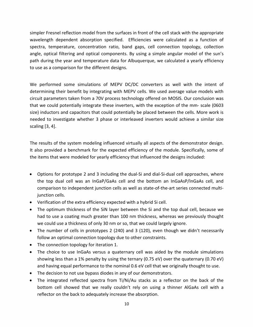
The tunnel junction design for this cell would be a tradeoff between optical loss and electrical performance. Narrow bandgap material can be more heavily doped leading to reduce resistance in the tunnel junction. However, if the bandgap is less than the cell above it in the optical path it will induce additional optical loss. We explored tunnel junctions made from InGaAs, InGaAsP and a combination of InGaAsP. The final design implemented a p-InGaAs/n-InGaAsP tunnel junction as a tradeoff between optical and electrical losses. The I-V for this is in Figure 17.
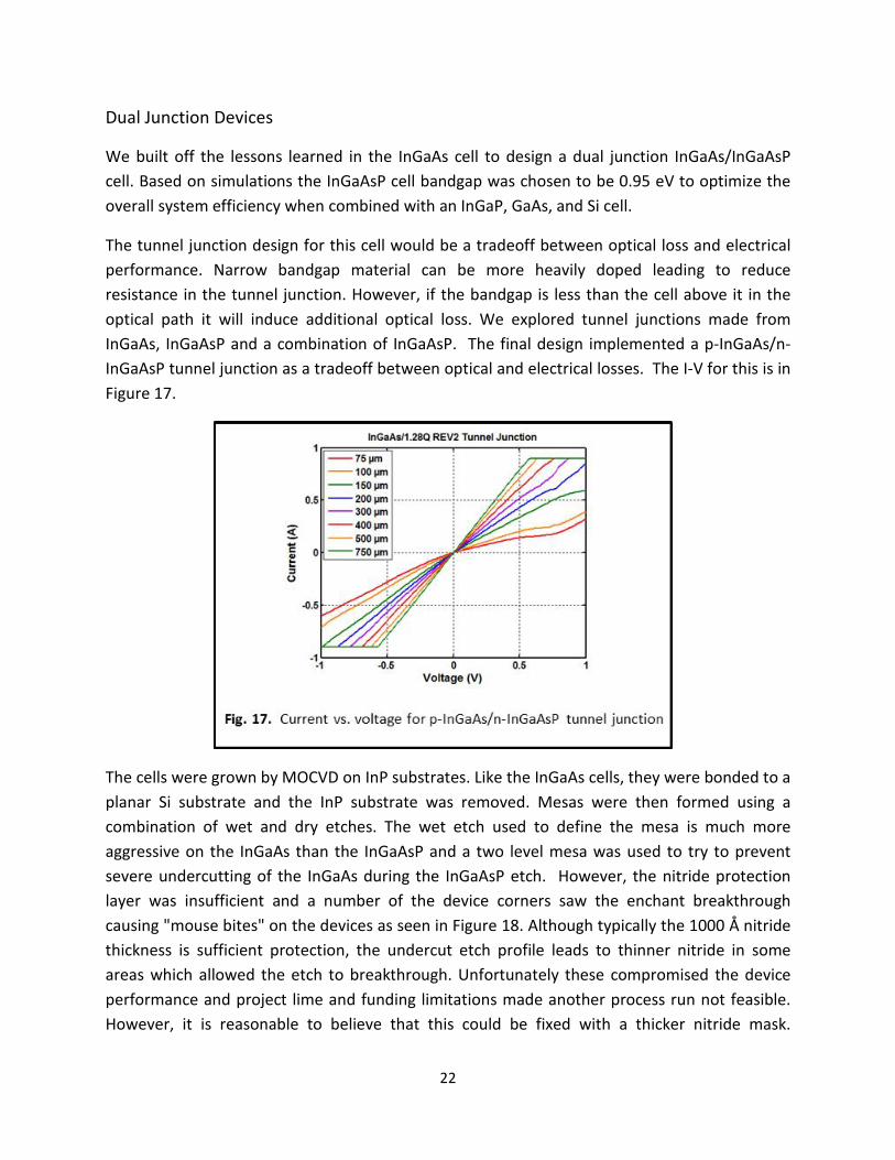
The cells were grown by MOCVD on InP substrates. Like the InGaAs cells, they were bonded to a planar Si substrate and the InP substrate was removed. Mesas were then formed using a combination of wet and dry etches. The wet etch used to define the mesa is much more aggressive on the InGaAs than the InGaAsP and a two level mesa was used to try to prevent severe undercutting of the InGaAs during the InGaAsP etch. However, the nitride protection layer was insufficient and a number of the device corners saw the enchant breakthrough causing "mouse bites" on the devices as seen in Figure 18. Although typically the 1000 Å nitride thickness is sufficient protection, the undercut etch profile leads to thinner nitride in some areas which allowed the etch to breakthrough. Unfortunately these compromised the device performance and project lime and funding limitations made another process run not feasible. However, it is reasonable to believe that this could be fixed with a thicker nitride mask.

23
Additionally, the material design could be verified by fabricating devices without bonding or removing them from the InP substrate. These are similar process issues to those encountered with the InGaAs cells and InGaP/GaAs cells and therefore it is reasonable to believe they could be overcome with minimal effort.
Summary Our results indicate that InP-based low bandgap cells can be intimately integrated with Si with degrading the device performance. This work is an important step towards achieving multi-junction MEPV cells spanning the solar spectrum. In particular, the 2.9% efficiency of the bonded InGaAs cell could be used to provide an important boost in performance to any multi-junction stack.
5.6 Cell Bonding and Release
III-V materials, especially InP-based and GaAs-based, have been the choice for high efficiency solar cells due to their direct bandgap. In particular multi-junction solar cells have been extensively used to increase efficiency. However, a limitation in increasing the efficiency of these cells is the defects introduced by the lattice mismatch between materials. Although there have been demonstrations of the growth of lattice mismatched materials on the same substrate to form multijunction cells, this approach requires tradeoffs in material quality and achievable bandgaps. Alternatively, wafer bonding has generated significant interest in allowing the heterogeneous integration of materials with mismatched lattice constants.

24
Using wafer bonding to integrate junctions with mismatched lattice constants a multi-junction cell can be designed to span a larger portion of the solar spectrum opening the opportunity to achieve higher efficiencies. Additionally, bonding makes it possible to electrically separate the junctions while maintaining a low loss optical path which allows the junctions to be individually optimized further increasing overall cell efficiency. Towards this goal, we have used a wafer bonded approach to demonstrate the integration of InGaAs solar cells on a Si substrate.
Towards this end we developed a wafer bonding technology which utilized a dielectric bond layer to provide electrical isolation. Additionally, this layer was designed to be optically thin to the wavelengths of interest. Another important aspect of the technology we developed was an aligned bonding process which allows the wafers to be partially processed prior to bond.
GaAs Bonding and Release The GaAs-based cells are grown on top of a stop etch layer, release layer, trench layer and stop etch layer as shown in Figure 19. Mesas are formed using wet and dry etching techniques depending on the cell structure. The mesas stop at the release layer and are coated in a protective nitride. This is the bonding layer so its thickness is chosen to be optically thin at ~300 Å. Inbetween the cell mesas the nitride is etched to reveal the release layer. This layer and the trench layer below it is etched in order to facilitate access for the release etchant after bond. The GaAs wafer undergoes an RTA at this point. Process development as indicated that this RTA is necessary to ensure the cells do not delaminate during high temperature processing later on. The mating Si wafer may or may not have had prior processing, however the bond area has a 100 Å thermal oxide and care has to be made that the bond area remains planar. The wafers are activated with an O2 plasma, aligned in a retrofitted MA6 contact mask aligner and bonded. This initial Van der Waals bond is strengthened by applying pressure and heat with a bladder bonder and hot plate. The thermal expansion mismatch between the GaAs and Si wafer limits the temperature and the wafers will crack beyond 150o C.

25
Following bonding the cells are released from the wafer using HCl. The release process takes ~90 min and having a 10-15 µm access channel has been essential to achieving realistic release time. Once the mesas are transferred to the Si wafer the rest of the processing takes place. This includes contact metal anneals at 420o C.
InP Bonding and Release The InP bonding process leveraged much of the work done with the GaAs cells. Our initial experiments showed that higher temperature bonds were possible due to the improved thermal mismatch between Si and InP compared with Si and GaAs. Initially a SiN thickness of 400 Å was used due to low optical losses to the long wavelengths of interest. Using the same activation and wafer prep steps as the GaAs we showed bonding of patterned and blank 2 inch and 3 inch wafers.
Two release layers were explored for InP. An InGaAs layer with InP as a stop etch and H2SO4:H2O2:H2O (1:1:10) as the removal chemistry. The alternative was an InP release layer using HCl as the release chemistry and utilizing InGaAs stop etch layers. Initially, the cell release was tested on unbonded cells to access the viability of the two approaches. During these tests it was discovered that protecting the substrate from the HCl was very difficult with all of our etch tests resulting in the substrate being attacked. Therefore, InGaAs was chosen as the release layer and the InP etch stop was thickened to account for the 1,500 to 1 selectivity between InGaAs and InP.
Substrate release tests were done on InP wafers bonded to Si wafers. The mesas were etched prior to bond and coated in 400 Å of nitride. The trench areas were then exposed and etched. The wafers were then activated and bonded. The bonded wafers were then put in release. After ~10 hours the substrate was not completely released but the wafers were able to be separated with a small amount of mechanical force. Inspection showed that although many of the mesas properly released the etch chemistry attacked the cells through pinholes in the thin nitride. Following this result, efforts were made to develop the bonding process with 3,300 Å of nitride which would give the same optical transmission and provide a better etch barrier. The thicker nitride made the bonding yield quite low for unknown reasons and should be explore further.
5.7 Optics Overview
1) The purpose of the optics is to inexpensively provide concentrated sunlight to huge arrays of sub-millimeter-sized photovoltaic cells. This requires arrays of close-packed lenses which will have to be mass-produced. We have chosen a solar concentration of 200X which reduces the

26
amount of PV material by that amount. This allows us to consider using III-V materials in addition to silicon. This increases the sunlight-to-electricity conversion efficiency dramatically. It also reduces the balance of system costs since less collection area is required for the same power output.
With a 200X concentration, the PV system must be mounted on a solar tracker. We minimize the tracker cost by designing the optics to operate well, even when there is a modest pointing error. A ±1.50 operating range seems to be adequate for most coarse sun trackers, even in the presence of wind gusts and seasonal temperature swings.
2) The challenge in designing the micro-optical arrays is to choose an optical design that can be inexpensively manufactured and will give good performance. This includes choosing the lens materials, the forming methods, assembly methods, and the needed optical performance. There is also an interaction with the substrate upon which the PV cells are mounted.
There are a number of optical plastics that can be used to form lenses by molding or casting, e.g. polycarbonate, PMMA (Polymethylmethacrylate) or PDMS (Polydimethylsiloxane, a.k.a. Silicone). Unfortunately polymers have thermal coefficients of expansion (CTE) that are an order of magnitude larger than any rigid substrate for the PV cells. Both polycarbonate and PMMA are stiff enough that any significant thermal expansion will cause them to de-bond if they are attached to a glass or silicon PV substrate. Alternatively, if a lens array “floats” relative to its PV substrate, then temperature changes will cause the lens array to grow laterally relative to the PV cells. This misalignment would be unacceptable for arrays larger than ~10 mm in size. PDMS also has a large CTE, but its Young’s modulus (rubber-like) is very low which allows an alternate design scheme.
3) How those challenges were addressed

27
After many design starts, we realized that a single PDMS lens cast directly on top of the substrate holding the PV cells could give a solar concentration of 200X. This design, shown in the Figure 20 above, also has adequate field of view, FOV=±1.70. PDMS has a large thermal expansion with CTE=340E-6 per 0C and also the refractive index decreases dramatically as the temperature rises and the wavelength increases. In spite of these effects, the theoretical design predicts that only 1-2% of the sunlight (for pointing angles within FOV<±10) will be vignetted. This is for a spectral band of 400nm to 1400nm and over the temperature range of 20C to 60C. (About 10% of the light will be lost at FOV=1.70.)
The PDMS lens arrays are cast on the PV substrates after all of the wiring is complete. This requires a very accurately machined mold, an assembly procedure, and precise alignment. The aluminum mold is about 50mmx50mm and contains 120 micro-lenses. The lenses were first machined to within 25μm of the final shape. Then they were diamond-turned to achieve a wavefront error <10μm which should produce good imagery, and a surface finish of ~10nm which was expected to scatter ~0.2%. Note that these lenses are spaced 3.5mm apart.
There are numerous assembly steps required before the lenses are cast (Fig. 21). The edges of the PV substrate have to be precisely ground so they can act as fiducial surfaces. The glass plate behind the PV substrate has to be glued on using PDMS to minimize stresses, and a Macor frame has to be used as the sidewalls of the mold. These sidewalls also prevent the PDMS from expanding laterally upon heating and cooling when the unit is later taken into the field. Finally, the glass cover is glued to the Macor frame. There are several bonds made during the assembly that keeps water and dust from entering the enclosure.
4) Key results
Actual Prototype 3 hardware has been shown to contain errors which can be corrected in another iteration. 1.) Alignment error exists between the cells and lenses at a level that can be

28
corrected in fixture changes 2.) The lens mold was not Teflon coated so there were a number of “pull-outs” on the lens surface which scattered light out of the focal blur. A careful cleaning of the mold and a Teflon coating should fix this problem. 3.) The system transmission was about 70% while we expected it to be ~85%. This is partly due to the “pull outs”, misalignment, and possibly some defocus. Based on the results of Prototype-2 described below, we expect to be able to fix all of these issues.
The Prototype 2 system would have been more costly to build than Prototype-3, so we tested it but did not pursue the architecture which is shown in Fig. 22. The system’s focal spot diameter was found to be DProto-2=66μm and the system transmission was 88.4%, even though the front glass and the rear surface did not have AR coatings. We would expect that the efficiency would be ~93% with these coatings.
5) The impact of those results
The overall results from Prototype-3 are disappointing but there are some bright spots. The imaging was examined using an earlier lens array. The diameter of the focal blur was found to be DProto-3=75μm so the lens prescription must be OK. Another issue worth reviewing is the refractive index of the PDMS. It may change more than we expect, though the design anticipates the immersed image height to vary by ±(Δn)/n ~ ±8%.
While the fabrication team was building Prototype-3, the design team was looking for further improvements. We have new designs that should reduce the PDMS cost from ~$40/m2 for

29
Prototype-3 to between $12/m2 to $20/m2 without making the system more difficult to fabricate.
5.8 Advanced Optical System Designs (University of Delaware)
Novel micro-concentrator concepts and designs are developed by University of Delaware and Sandia National Laboratories in the microsystems-enabled photovoltaics (MEPV) program. A new decentralized micro-optical concentrator concept using low-cost molded micro-optics is proposed and developed. The concept leads to compact micro-optical designs that can potentially achieve a high concentration-acceptance product (CAP =
ingC θsin ) and meanwhile
provide low intensity illumination on the receiver as well as inside the optical components in order to improve efficiency and avoid damages to the plastic components.
The basic concept is schematically depicted in Fig. 23 (a). Key notions of the 2-element micro-optical concentrator are toroidal primary and/or secondary refractive surfaces and a reflective cone structure on the secondary optical element. The toroidal lens surface re-distributes its focus spot and generates donut-shaped illumination patterns on its focal plane. The re-distributed irradiation pattern reduces peak optical intensity and eliminates hot spots on the receiver as well as inside the plastic optical components. The secondary optical element further incorporates a reflective cone structure (based on either a reflective coating or total internal reflection (TIR)) which immerses the micro-scale solar cell via an index matching layer in order to enhance the concentration-acceptance angle product. An array design is illustrated in Fig. 23 (d) where the arrayed primary and secondary micro-optical concentrators are molded in two large area optical plates and integrated with micro-scale solar cell arrays. As depicted in Fig. 23 (e), by varying the decenter distance of the toroidal rear lens surface, the peak optical intensity on the solar cells can be significantly reduced while keeping a desirable transmission and acceptance angle.
Several micro-optical concentrator systems are designed based on the toroidal-cone concept, taking into account practical considerations on fabrication and integration with commercially available tools. Design 1 is shown in Fig. 24: the 2-stage micro-concentrating optical module consists of two injection-molded polycarbonate lens arrays assembled together with a Sylgard®184 PDMS filler layer between the optical plates. The secondary optic further incorporates a toroidal lens surface and cone structure consisting of 6 flat facets which couple incident light onto the hexagonal micro-PV cell. The minimum spacing between the primary and secondary optics is determined by thermo-mechanical analyses to reduce the stress load in the PDMS layer to avoid cohesive and adhesive failure during temperature variance. The optical module is designed to have a 150X geometric concentration ratio with a hexagonal primary lens aperture 2.75mm in diameter and a hexagonal PV cell 225µm in diameter. Monte

30
Carlo ray-trace simulations with a simulated solar source show an on-axis optical transmission of ~92% and a peak irradiance on the receiver of ~190 suns. The acceptance angle (90% of peak) of this design is ±4.9°, yielding a CAP of ~1. The optical system is optimized to avoid hot spots at oblique incidence within the field-of-view. Fig. 24 (d) shows another version of Design 1, in which a low-aspect-ratio cone structure is used.
Design 2 (shown in Fig. 25) consists of toroidal lens surfaces on both primary and secondary optical elements and an air-gap between the two components. PDMS is chosen as the material of the optical elements which can be directly cast on glass plates. The TIR-based cone structure is modeled with 100µm-radius rounded corners and an aspect ratio of ~3:1. Two designs based on the same architecture achieve a geometric concentration ratio of 400X with an acceptance angle of ±2.4° (CAP = 0.84) and a concentration of 600X with an acceptance angle of ±2° (CAP = 0.85). Both Design 1 and 2 provide considerable improvement on the concentration ratio while maintaining a reasonable acceptance angle tolerant to most low-cost trackers (1° ~1.5° tracking accuracy).
The performance of the above designs is compared with existing small-form-factor solar concentrators on the market, shown in Table 2. Note that for a given optical architecture, the concentration-acceptance product (CAP) is nearly invariant for different designs and therefore is a key merit function to evaluate concentrating optical systems. The comparison clearly indicates that the UD-Sandia developed toroidal-cone approach outperforms state-of-the-art technologies and is designed for high manufacturability and low cost.
Table 2. Comparison of UD-Sandia micro-concentrators with flat CPV technologies on the market
Suncore SolFocus Semprius LPI Abengoa UD-Sandia UD-Sandia
Concentration 1090X 850X 1600X 710X 1000X 400X/600X 150X
Acceptance Angle ±0.7° ±0.85° ±0.75° ±1.27° ±1.3° ±2.4°/±2° ±4.9°
CAP =ingC θsin 0.4 0.43 0.52 0.59 0.72 0.85 1

31
(a) (e) Fig. 23. (a) Schematic of basic toroidal-cone concentrator concept. (b) Top view of an exemplary toroidal surface. The original optical axis of a lens surface is decentralized from the mechanical axis along a continuous circular trajectory (indicated by the red circle) with rotational symmetry. (c) Perspective view of a toroidal surface. (d) Array design where micro-concentrator arrays are molded in two large area optical plates and integrated with micro-scale solar cell arrays. (e) Peak optical irradiation on solar cell vs. optical axis decenter distance of toroidal secondary lens.
ToroidalSurface
Decentralized Optical Axes
Primary Concentrator
Sunlight
Secondary Concentrator
Solar Cell
Reflective Cone
Decentralized Optical Axes
(c)(b)
(d)
0
200
400
600
800
1000
1200
1400
1600
0.45 0.7 0.95 1.2 1.45
Peak
Opt
ical
Con
cent
ratio
n (S
un)
Lateral Decenter Distance of Optical Axis (mm)
Low Optical Intensity on PV cell
Peak Optical Concentration on PV Cell at Normal Incidence
Fig. 24. (a) 150X design with a toroidal lens surface on secondary optic and ray-trace simulation results. (b) On-axis irradiation pattern on PV cell. (c) Simulated optical transmission vs. angle of incidence. An acceptance angle of ±4.9° is achieved at a geometric concentration of 150X (CAP = 1). (d) Design with a cone with a low aspect ratio and rounded corners (150X, ±5° FOV, CAP = 0.85).
00.10.20.30.40.50.60.70.80.9
1
0 1 2 3 4 5 6 7 8
Opt
ical
Tra
nsm
issi
on
Incidence Angle (Degree)
X-directionY-direction
0.561.1
(a) (c)
PC
PDMSPC
PV Cell
θin = 5°
Unit: mm
θin = 0°
(b)
Glass
Air
7.1
1
PC
PDMS
PC
Glass
(d)
Fig. 25. (a) Schematic of double-toroidal-cone concept (b) Design with a 600X concentration and ±2° FOV (CAP = 0.85) and simulation result. (c) 0° incidence angle. (d) 2° incidence angle. (e)Simulated optical transmission vs. angle of incidence. (f) Exemplary toroidal lens surface and cone structure with 100µm-radius rounded corners.
2°
0°
0
0.2
0.4
0.6
0.8
1
0 1 2 3 4 5
Opt
ical
Tra
nsm
issi
on
Incidence Angle (Deg)
(f)(b)
(c)
(d)
(e)Toroidal Front and Rear Lenses
CellCone structure
(a)

32
5.9 Optics Manufacturing
Optics manufacturing is critical to the realization of MEPV systems as micro-optic arrays must be accurately and inexpensively produced at scales appropriate for commercial PV applications. Form and alignment tolerances for the three MEPV optical designs ranged from 10 to 50 µm, a challenging requirement when scaled to large array sizes. While commercial scale PV requires collection areas measured in square meters, the MEPV arrays were roughly 50 mm by 50 mm. These prototypes still contain one to two hundred individual optic surfaces; however, one to two orders of magnitude larger than pre-Grand Challenge prototypes [8]. Fabrication was further restricted to demonstrate the feasibility of scalable techniques amenable to mass production at costs consistent with the Sunshot goal of $1 per watt peak. As a result, cost modeling constrained production quantity optic costs, i.e. material and fabrication, to less than $10/m2.
Demonstrating inexpensive processes for the high volume manufacturing of MEPV optics involves multiple fabrication challenges. Cost targets motivated the precision replication of polymer lenses since direct machining of polymer or glass is neither scalable nor cost effective. A first step is the generation of molds with aspheric surface geometries representing the negative of the desired optic shape. These molds must have surface form accuracies of 5 to 10 µm, surface finish better than 30 nm Ra, and surface location accuracy better than 5 µm across a large array format. Physical limitations on tool geometry introduced design constraints on optic surface slopes, total sag and aspect ratio. Anticipated concerns at the onset of the project also included potentials for unacceptable tool wear rates and excessive machining cycle times. The precision replication of accurate micro-arrays, whether by injection molding or casting, involves additional challenges which include mold filling, material shrinkage, process throughput, part release and part distortion. Each of these challenges was exacerbated by the high aspect ratio part geometries necessary for MEPV arrays.
Mold fabrication was demonstrated by combing precision micro-milling with ultra-precision diamond milling [9]. 6061-T6 was used for development molds due to its availability, machinability and durability for the desired small number of optic samples. Rough mold machining was performed on a 5-axis, Yasda YMC 430 micro-machining center in three to four hours with material left for final machining. A single final finish pass was then performed on a Moore 350FG diamond turning machine using a diamond milling tool to achieve the final optical surface. While the form and finish are improved through diamond machining, process throughput is significantly slower; typically requiring one hour per lens surface. The combination of the two processes, however, reduced process cycle times and tool wear for improved optic surface consistency across the mold pattern.

33
Two different replication techniques were explored to generate micro-optic arrays, injection molding for prototype 2 and casting for prototype 3. Injection molding was performed in partnership with an external collaborator, Greenlight Optics (Cincinnati, OH). In-plane material shrinkage was measured using test parts and compensated in a final mold design. Final part surface form was better than 10 µm, with surface finish consistent with the 30 nm Ra finish of the mold. As anticipated, the high aspect ratio of the micro-array, almost 20 to 1, presented the greatest difficulty in molding as more than 100 µm of deformation was observed in final parts. Such deformation created difficulties during assembly and introduced stresses which could produce failures in thermally cycled environments. Casting prototype 3 PDMS lenses eliminated several problems, but also introduced new challenges. Process development occurred at Sandia to improve process control and flexibility. The low cure temperature and soft elastic modulus of PDMS eliminated issues with mold filling and part deformation as the optic aspect ratio was also reduced to 10 to 1. Part release and surface contamination were observed to present new challenges during initial prototypes; however, and must be addressed in future work.
Each optical surface introduces a change in the refractive index, n, between two materials, and a subsequent loss of transmitted energy from reflection. An air to glass transition, for example, loses approximately 4% of the available photon flux between 350 and 1100 nm from reflection. For prototype 2, the glass to polycarbonate (n = 1.52 to 1.60) and polycarbonate to PDMS interfaces (n = 1.60 to 1.41) result in minimal reflective losses, so no changes were considered for either interface. The air side of the prototype 2 glass, however, was coated with an anti-reflective (AR) thin film coating stack designed for direct deposition. A six layer stack of high and low refractive index materials (tantalum and silicon oxide) was designed to reduce the surface reflection to 1.4% as seen below. A similar coating was used on both sides of the front cover glass in prototype 3 since both contact air. The PDMS to air (n = 1.41 to 1.00) interface for the lenses on prototype 3 results in a 3.5% reflection. The soft elastic surface of the PDMS represents a challenge for the typical ceramic thin film AR coating. A molded set of cones, smaller than the solar wavelength and similar to a moth’s eye, formed in the PDMS would be a very effective AR layer. Etched shapes were produced successfully into aluminum using an anodic aluminum oxide technique. Replicating these features in the PDMS, however, requires additional development.
In summary, the viability of manufacturing high performance MEPV micro-optic arrays in a scalable, inexpensive form has been demonstrated through the generation of three prototype designs. Micro-arrays have been replicated in a mass producible form via molding and casting; while ultra-precision fabrication has demonstrated the capability to generate hundreds of lens surfaces with form, finish and location accuracy which satisfy design requirements. While challenges remain to achieve production scales necessary for commercial applications, it is
34
believed the present work has demonstrated the process fundamentals and viability necessary to further development investments.
5.8 Module Opto-Mechanical Design The integration of MEPV optics and cells into a module must satisfy a range of design constraints and performance requirements that span opto-mechanical, thermo-mechanical, electro-optical and material disciplines. The MEPV module must provide a robust, reliable package that withstands both process and operating environments. It must also be scalable to sizes and costs appropriate for commercial applications. Large micro-optic arrays must be assembled and aligned to their corresponding cell arrays, while package structures and materials must simultaneously provide environmental barriers and electrical connections to the external world. Three modules designs have been prototyped to explore and demonstrate the integration of critical MEPV elements.
Initial design challenges focused on the assembly and alignment of micro-optic and cell arrays. Planar (XY) alignment tolerances for a single lens or cell element were approximately 10 to 20

35
µm, while axial (Z) alignment tolerances ranged from 25-50 µm. Such tolerances are generally straightforward for the fabrication and assembly of conventional optics with a single beam path. They become much more challenging, however, for large array assemblies with hundreds or even thousands of beam paths. Although active assembly techniques are commonly utilized in optics; they can be slow, expensive and prohibitively complex for arrays with numerous degrees of freedom. Passive assembly, therefore, was used in all three prototype designs to reduce assembly complexity, albeit at the expense of tighter fabrication tolerances for assembled components.
Coefficient of thermal expansion (CTE) differences between the polymer optics and other metal, glass or semiconductor materials in the module represented the predominant challenge faced during module design. During exposure to temperature changes or gradients, CTE differences generate short term optical loses due to package distortion and lens to cell misalignment. Longer term optical loses are also anticipated due to thermal stresses which degrade materials and/or interfaces. Athermalized alignment features minimize expansion lengths by establishing zero expansion locations at the center of the optic and cell arrays. Thermo-mechanical analyses were also utilized to guide material selection and design material interfaces to reduce stresses, distortion and misalignment from CTE differentials.
Three module designs have been developed and demonstrated, each corresponding to one of the prototype optical designs. Each design accommodated the intent of their optical designs, and built on experience from prior work to improve their performance, ease their assembly or reduce their complexity. Prototype 1 focused on demonstrating the integration of optics and cells in a functional module and did not provide any protection against external environments [10]. Cells were arrayed on an FR4 board and aligned to optics mechanically using dowel pins and spacers in a pseudo-kinematic arrangement. The objective for prototype 2 was to deliver a module with improved performance and robustness to environments that could potentially represent a commercial product. Cells arrays were explored using both polyimide flex and hybrid silicon as the base array substrate. Optic and cell arrays were aligned passively using monolithic alignment features that were designed and molded directly into the optic arrays. PDMS and urethane adhesive layers functioned as optical fillers and as low elastic modulus interfaces to alleviate the CTE mismatches between the polycarbonate lens arrays, the semiconductor cells and the exterior glass. Thermo-mechanical analyses were utilized to modify the optical design to minimize stresses in the PDMS fill layer, and to verify module integrity at the glass and polycarbonate interfaces. Prototype 2 is extremely robust to the external environment as all gaps are filled by PDMS, and a barrier sealant is applied to the perimeter of the module. Prototype 3 was designed to reduce module complexity, tolerances and cost. A single PDMS lens array is cast directly onto a hybrid silicon cell array. Optic-cell alignment and assembly is based on fixtures that use the glass substrate as a precision mechanical reference.

36
Process metrology has verified that assembly accuracies meet performance requirements. Machinable Macor is used as the package frame to provide a better CTE match to the glass and silicon in the module. Thermo-mechanical analyses were again utilized to design the module package, to inform the assembly process, and to verify material interface robustness under temperature changes. Protection against the environment is achieved by back-filling the entire package with nitrogen, and by sealing the glass to the Macor frame with polymeric adhesives.
The integration of micro-optic arrays, cell arrays, electronics and materials into working modules has been a significant success for the demonstration of the MEPV paradigm and system architecture. Cost modeling has shown that prototype 3 presents a realistic path to achieving utility scale power below the Sunshot target of $1 per watt peak. Module development has been a critical piece of this accomplishment as work has successfully integrated optic and cell arrays with improved performance and decreased complexity and cost.

37
5.9 Prototype Characterization (University of Delaware)
This report summarizes the laboratory and field characterization of MEPV Prototype 2 and Prototype 3 modules performed at University of Delaware.
Prototype 2 optical module test
The prototype 2 module is designed for a 100X geometric concentration ratio (250µm-diameter solar cells) and a ±2.5° acceptance angle. As shown in Fig. 28, the test module consists of two injection-molded polycarbonate lens arrays assembled together with a Sylgard®184 PDMS filler layer between the optical plates. The unit cells are arranged in a 15x16 hexagonal array (close to 100% fill factor) with 2.381mm and 2.058mm pitch spacing respectively. Spectroscopy measurements of the optical module using a Perkin Elmer Lambda 650 UV-Vis-IR spectrophotometer shows an AM1.5G weighted bulk transmission of ~87% over
400nm~1127nm (an air-module-air measurement without AR coatings), as illustrated in Fig. 29. Using a halogen lamp white light source that simulates the solar disk’s angular extent, spot array at the output plane of the concentrator module is generated and captured by a camera (Fig. 30). Spot diagram shows an averaged focus spot size of ~50µm (FWHM).

38
In order to accurately simulate the tested MEPV optical module, a 3D optical simulation model is constructed (Fig. 31), which incorporates measured data from fabricated components (e.g., refractive indices, absorption, molded lens profiles, component thicknesses and distortions, etc.). Ray-trace simulations show that the air-module-air bulk transmission of the tested module is ~88%, with most of the optical power confined within the 250µm cell region.

39
Concentrated transmission of the optical module is measured outdoor with the optical module mounted on a high-precision solar tracker, as depicted in Fig. 32 In order to the capture the concentrated sunlight that falls onto the designated cell region only, blocking masks with windows simulating the 250µm-diameter cells are assembled onto the optical module’s rear surface via a PDMS layer.
Fig. 33 shows the measured outdoor concentrated transmission (air-module-air transmission) onto the cell region under various radiation conditions, which indicates a good agreement with the simulation model. The concentrated transmission under direct radiation is ~86.7%. With appropriate AR coatings and solar cells immersed in the secondary optic via an index matching layer, it is projected from optical simulations that the transmission of such micro-concentrator modules can achieve 93%, indicating the potential of the current injection molding and assembly approaches to realize high efficiency, low cost and robust micro-optical concentrator modules.
The acceptance angle of the optical module is measured outdoor using a fully packaged module with PV cells integrated with the micro-concentrator array. As shown in Fig. 34 , the prototype 2 optics achieves an on-sun acceptance angle of ~4.5° (full width at 90% of peak) and ~6.3° (FWHM), providing sufficient angular tolerant to most low cost trackers (1°~1.5° tracking accuracy). Compared to the simulation model, the asymmetric shape of the experimental

40
results is a possible indication of slight lateral misalignments between the front and rear optical components.
Fig. 35 summarizes the setup and results of outdoor electrical performance characterization of the packaged prototype 2 module (measured at Newark, DE).
Prototype 3 optical module test
The prototype 3 optical module is designed for a 200X geometric concentration ratio with a single PDMS lens element and arranged in a closely packed 10×12 lens array (Fig. 36 (a)). Spectroscopy measurements are performed on the prototype 3 optical module (air-module-air, no AR coatings), showing an AM1.5G weighted bulk transmission of ~76% over 400nm~1127nm, as illustrated in Fig. 37. The relatively low transmission compared to simulation results are attributed to surface finish and defects/pull-outs of the lens surface possibly due to the fabrication process. Spot array generated at the cell plane using an indoor simulated source shows a focus spot size of ~60µm (FWHM), indicating that the molded lens array has a desirable lens profile (Fig. 36 (b)).

41
5.10 Module Testing and results
The goal of module testing was to obtain an accurate measurement of whole assemblies (cells, optics, and packaging) in a real environment under the sun.
The challenges in accomplishing that goal were in assembly, low yield and variability of performance on cells, power extraction, robust packaging, the size of the module tested.
Power extraction of the cells to the outside world was implemented using PCB boards connected by conductive epoxy or by wire bonds to the cells or silicon pieces. These techniques worked but compromised reliability in an outdoor environment. To account for the small size of the module, special fixtures were designed to fit the modules in the tracker, also special loads in the resistor bank were used to accommodate for the low currents of these modules. More details about the testing of prototype 1 (Figures 38 and 39) can be found in [11, 12]

42
In order to avoid leaving airgaps, Prototype II (Figure 40) moved to a solid lens design with a hermetic seal. This unit made to be used with a PCB board to fan out the connections into a larger connector. Prototype 2 had designs in which cells could be measured individually and designs where cells were tested in groups of series and parallel.
Table 3 Outdoor cell measurements on the University of Delaware tracker.
Cell Pmax (mW) Isc (uA) Voc (V) Global (W/m2) Direct (W/m2) FF (%) Eff. (%)
5 747.4 365.0 2.40 1023 868 85.3% 17.54% 13 860.0 418.0 2.41 1095 860 85.4% 20.36%
14 791.9 386.0 2.41 966 833 85.3% 19.36% 15 809.5 394.0 2.41 993 847 85.4% 19.47% 18 619.5 307.0 2.36 994 872 85.5% 14.47%
20 803.9 398.0 2.38 1006 872 84.8% 18.77%
The Table 3 shows outdoor efficiencies of single cells with full packaging and concentrating lenses under one sun. These cells were tested mounted in a tracker at the University of Delaware (Fig. 41). Efficiencies up to 20% were shown considering all optical losses. In order to characterize multiple cells at a time, the module version with grouped cells was used. This module was mounted to a PCB board, wirebonded, sealed and interconnected. The prototype was able to produce several strings with interconnected cells. The performance was degraded because of the low yield in cells (the lowest performing cell limits the whole string).
Through this measurement, we were able to demonstrate the capability of building and testing small and think micro-concentrators using conventional solar technology for characterization
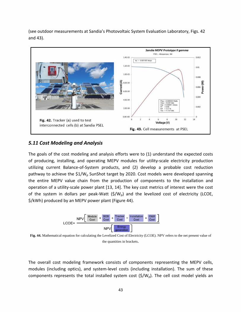
43
(see outdoor measurements at Sandia’s Photovoltaic System Evaluation Laboratory, Figs. 42 and 43).
5.11 Cost Modeling and Analysis
The goals of the cost modeling and analysis efforts were to (1) understand the expected costs of producing, installing, and operating MEPV modules for utility-scale electricity production utilizing current Balance-of-System products, and (2) develop a probable cost reduction pathway to achieve the $1/Wp SunShot target by 2020. Cost models were developed spanning the entire MEPV value chain from the production of components to the installation and operation of a utility-scale power plant [13, 14]. The key cost metrics of interest were the cost of the system in dollars per peak-Watt ($/Wp) and the levelized cost of electricity (LCOE, $/kWh) produced by an MEPV power plant (Figure 44).
Fig. 44. Mathematical equation for calculating the Levelized Cost of Electricity (LCOE). NPV refers to the net present value of
the quantities in brackets.
The overall cost modeling framework consists of components representing the MEPV cells, modules (including optics), and system-level costs (including installation). The sum of these components represents the total installed system cost ($/Wp). The cell cost model yields an

44
estimate of the cost ($/wafer or $/cm2) to fabricate cells based on an industrial-scale cell fabrication process flow. The cost of each of the more than 200 steps in the process was estimated based on contributions from raw materials, capital costs, labor, facilities overhead, and consumables. Model input parameters, including tool cost and performance parameters (e.g., throughput, capital costs, labor requirements, materials and energy consumption, and footprint) and materials costs were obtained through direct inquiries with tool vendors. The cell fabrication cost serves as an input to the module cost model, which calculates the expected module cost for a given optical concentration ratio and cell size, based on modeled and empirical-based estimates regarding the efficiency of light capture by the optics and conversion to electricity by the cells. The module cost and efficiency estimates in turn serve as inputs to the total system cost model.
Many of the module- and system- level costs for MEPV are similar to those for conventional non-concentrating Si-based PV; current costs and projections to 2020 for these components and processes were taken from reports by the National Renewable Energy Laboratory (NREL) [15, 16].
The early-stage nature of the MEPV technology presented a significant challenge, as many aspects of MEPV module design and production were initially unknown or ill-defined, and iteratively evolved over the course of the Grand Challenge. To address this challenge, the cost modeling structure was designed to be flexible and adaptable to design changes. In addition, cost estimates were augmented with sensitivity studies and trade-off analyses to identify parameters governing system cost and compare proposed designs. The insights gained from these analyses were employed to guide the design of successive prototypes, identify areas for further research and development, and inform the selection of important system parameters such as concentration ratio and cell size.
The final estimates of current costs for MEPV modules are listed in Table 4, along with 2020 cost projections based on anticipated cost reductions. Current and 2020 cost estimates of installed MEPV systems are shown in Figure 45. Current cost estimates are based on a design similar to Prototype 3, with either single-junction silicon cells, InGaP/GaAs/Si triple-junction cells, or InGaP/GaAs/Si/ InGaAsP/ InGaAs five-junction cells. For the 2020 cost projections, these same cells were paired with a “Prototype 4” module that featured lower materials usage. The 2020 cost of systems employing singulated inverted metamorphic multijunction (IMM) cells was also estimated. Based on potential cost reductions identified at the cell- module-, and system-level, MEPV is positioned to approach the $1/Wp target by 2020.

45
Table 4. Estimated MEPV module costs employing Si, InGaP/GaAs/Si, and InGaP/GaAs/Si/ InGaAsP/ InGaAs PV cells. Current cost estimates are based on a module design similar to Prototype 3 (module efficiency = 33.2%); projected 2020 costs assume a Prototype 4 module design (module efficiency = 38.7%).
PV Cells Estimate of Current Module Cost
Based on Prototype 3 Module Projected 2020 Module Cost
Based on Prototype 4 Module Si cells $1.22/Wp $0.51/Wp InGaP:GaAs/Si $1.44/Wp $0.46/Wp InGaP/GaAs/Si/ InGaAsP/ InGaAs $1.83/Wp $0.51/Wp IMM - $0.36/Wp
Fig. 45. Installed system cost estimates based on MEPV module costs listed in Table 4.
6.0 Intellectual Property
MEPV has secured intellectual property rights, including patent rights, based on a portfolio strategy conscious of technical, business, and legal input. Various aspects of MEPV are the subject of pending patent applications and issued patents in the United States. Some cases are also under foreign patent consideration. Even after completion of the Grand Challenge period, intellectual property efforts will still continue. At the time of this report, there are 49 patents either issues or in process.

46
7.0 Presentations
This section comprises a list of presentations concerning the MEPV project. Internal presentations (e.g. advisory board meetings, corporate visits, etc) and minor presentations may not be included. Invited presentations are denoted with an *.
Calendar Year 2011 1. C. Tapia, J. L. Cruz-Campa, G. N. Nielson, “Characterization of ZnxCd(1-x)Te graded bandgap
nanoarrays for solar cell applications” presented at Annual NINE Student Workshop, Albuquerque, NM, Jul 27, 2011.
2. B.A. Aguirre, J. L. Cruz-Campa, G. N. Nielson, “Creation of Nanotemplates by Nanoimprint and Interferometric Lithography for ZnxCd(1-x)Te Based Solar Cells” presented at Annual NINE Student Workshop, Albuquerque, NM, Jul 27, 2011.
3. G.N. Nielson, “Microsystem-enabled Photovoltaics (MEPV): Taking Advantage of Scaling Benefits in Solar Power” presented at Mesa External Advisory Board, Albuquerque, NM, Jan 17-21, 2011.
4. J. S. Nelson, “Microsystems Enabled Photovoltaics (MEPV) Grand Challenge” presented at MEPV Solar Grand Challenge, Albuquerque, NM, Dec 15, 2011.
Calendar Year 2012 1. (Invited)* G.N. Nielson, M. Okandan, P. J. Resnick, C. A. Sanchez, P. J. Clews, T. Pluym, W. C.
Sweatt, A. L. Lentine, V. P. Gupta, “Efectos de miniaturización en celdas fotovoltaicas” presented at Invited speaker for semester talks at MICRONA, Universidad Veracruzana, Veracruz, Veracruz, Mexico, Dec 29-30, 2012.
2. A.L. Schauer, M. Okandan, G. N. Nielson, E. Langlois, M. Shaw, P. J. Resnick, R. C. Givler, J. M. Hochrein, A. I. Young, “MEMS Photoacoustic IR Spectroscopy” presented at MEMS Photoacoustic IR Spectroscopy, Albuquerque, NM, Feb 13, 2012.
3. Next Generation Photovoltaic Cells and Systems through MEMS Technology,” ECS Transactions, G. N. Nielson, et al., 2012 (invited).
4. “Exploiting Scale Effects to Create Next-Generation Photovoltaic Cells and Systems,” UNM Chapter IEEE Photonics Society, G. N. Nielson, 2012 (invited).
5. “Solar Glitter – Microsystems Enabled Photovoltaic,” Proc. of APS March Meeting, G. N. Nielson, 2012 (invited).
6. “Microscale Photovoltaic Cells to Exploit Cell, Module, and System Scaling Benefits,” 2012 Energy Materials Nanotechnology Meeting, G. N. Nielson, et al., 2012 (invited).
7. “Exploiting Scale Effects to Create Next-Generation Photovoltaic Cells and Systems,” University of Vermont, G. N. Nielson, 2012 (invited).
8. “Exploiting Scale Effects to Create Next-Generation Photovoltaic Cells and Systems,” Massachusetts Institute of Technology, G. N. Nielson, 2011.

47
Calendar Year 2013 1. S. M. Paap, V. P. Gupta, “Microsystems Enabled Photovoltaics (MEPV) System Cost Modeling”
presented at Future Seminars at Public Events, Albuquerque, NM, Mar 8-12, 2013.
2. B. H. Jared, M. P. Saavedra, B. J. Anderson, W. C. Sweatt, G. N. Nielson, M. Okandan, “Micro-Optic Fabrication for Microsystems-Enabled Photovoltaics,” ASPE Annual Meeting, St. Paul, MN, Oct 21-24, 2013
3. G. N. Nielson, “Solar Photovoltaic Cell, Module, and System Performance and Functionality Enhancement through MEMS Technologies,” 2013 MRS Fall Meeting and Exhibit, Boston, MA, Dec 1-6, 2013
4. G. N. Nielson, "Innovative CPV approaches to reduce balance of system costs," 5th Concentrated Photovoltaic Summit, San Jose, USA, 2013.
5. B. H. Jared, M. P. Saavedra, B. J. Anderson, W. C. Sweatt, R. S. Goeke, G. N. Nielson, M. Okandan, B. Elisberg, D. Snively, J. Duncan, “Micro-Concentrators for a Microsystems-Enabled Photovoltaic System,” Optics for Solar Energy, Tuscon, AZ, Nov 4-6, 2013
6. G. N. Nielson, "New Tech for Resilient Distributed Generation," EPRI International Technology Innovation Summit, New York, USA, 2013.
7. D. D. Koleske, S. R. Lee, M. H. Crawford, K. C. Cross, J. M. Kempisty, and M. E. Coltrin, “Quantifying Surface Mounding of GaN and InGaN Thin Films,” poster presentation at 10th International Conference on Nitride Semiconductors, Washington, D.C, August 25-30, 2013.
8. J. S Nelson, “The Prospects for Cost-Competitive Photovoltaics: From Nanoscale Science to Macroscale Manufacturing,” GERA Workshop at the March APS Meeting, Baltimore, MD (3/17/2013). (invited)
9. J. S. Nelson, “Microsystems Enabled Photovoltaics: High-Efficiency Ultra-Flexible PV,” DARPA Workshop on R&D Opportunities for PV Portable and Transportable Power,” Golden, CO (1/15/2013). (invited)
10. G. N. Nielson, “Innovative CPV Approaches to reduce Balance of System Costs,” 5th Concentrated Photovoltaics Summit USA 2013, San Jose, CA (9/2013). (invited)
11. G. N. Nielson, “Microsystems Enabled Photovoltaics (MEPV),” Tech Connect World Summit & Innovation Showcase, Washington, DC (2013).
12. G. N. Nielson, “Enhanced Multijunction Cell and System Conversion Efficiency through Heterogeneous Microsystems Integration Techniques,” Optical Nanostructures and Advanced Materials for Photovoltaics, Optical Society of America (11/2012). (invited)
13. Jose Luis Cruz-Campa, “Celdas solares habilitadas por microfabricacion”, Invited Talk and opening speaker for 5th seminar of nanoelectronics and advanced design” INAOE, September 18th, 2013, Puebla, Mexico
14. Jose Luis Cruz-Campa “Solar Microsystems”, tech talk at The University of Texas at El Paso, September 13, 2013, El Paso, TX
15. Jose Luis Cruz-Campa Solar “Glitter, microsystems enabled photovoltaics”, University of Kansas, May 6, 2013, Laurence, KS
16. Jose Luis Cruz-Campa Invited talk “Efectos de miniaturizacion en celdas solares”, at the University of Veracruz, October 29-30, 2012, Veracruz, Mexico

48
17. Jose Luis Cruz-Campa “Solar Glitter, microsystems enabled PV”, at NM PBS Science Café, October 27, 2012, Albuquerque, NM.
Calendar Year 2014 1. G. N. Nielson, "Exploiting scale effects in photovoltaic cells, modules, and systems," ARPA-E
Microscale Photovoltaic Workshop, Arlington, VA, 2014.
2. J. L. Cruz-Campa, J. G. Cederberg, J. S. Nelson, G. N. Nielson, C. Alford, C. A. Sanchez, I. Luna, “Bonded InGaAs Cells for Microsystems Enabled Photovoltaics,” Photovoltaic Specialists Conference, Denver, CO, Jun 8-13, 2014.
3. M. P. Saavedra, W. C. Sweatt, G. N. Nielson, M. Okandan, B. Elisberg, B. Anderson, B. K. Miller, B. H. Jared, “Efficient micro-concentrator for microsystems-enabled photovoltaics,” American Society for Precision Engineering, Boston, MA, Nov 9-14, 2014
8.0 Publications
This section comprises a list of publications organized by category concerning the MEPV project. At the time of this writing a number of publications are still in the review, editing, and composition stages. A tentative list of these documents is provided for future reference.
Conference Proceedings Calendar Year 2011
1. M. Okandan, G. N. Nielson, “A New Energy Infrastructure: Building Blocks for the Next Industrial Revolution,” GovEnergy 2011, Cincinnati, OH, Aug 7-10, 2011, Sandia National Laboratories document SAND2011-6997 C.
2. G. N. Nielson, M. Okandan, B. H. Jared, A. L. Lentine “Concentrating Photo-Voltaic Systems Using Micro-Optics,” OSA's 2011 Renewable Energy and the Environment Meeting, Austin, TX, Nov 2-4, 2011, Sandia National Laboratories document SAND2011-4707 C.
3. J. L. Cruz-Campa, G. N. Nielson, M. Okandan, P. J. Resnick, C. A. Sanchez, P. J. Clews, W. C. Sweatt, A. L. Lentine, V. P. Gupta, “Microsystems enabled photovoltaics research at Sandia,” UNM ECE Graduate seminar, Albuquerque, NM, Nov 11, 2011, Sandia National Laboratories document SAND2011-8554 C.
4. J. L. Cruz-Campa, X. Zhou, J. L. Skinner, D. B. Burckel, C. A. Sanchez, G. N. Nielson, D. Zubia, J. Chavez, B. Aguirre, “Record breaking solar cells: a materials perspective,” 4th Annual Thin Film Solar Summit USA, San Francisco, CA, Dec 1-2, 2011, Sandia National Laboratories document SAND2011-9014 C.
5. J. L. Cruz-Campa, J. M. Lavin, C. D. James, C. A. Stewart, R. Kemp, G. N. Nielson, M. Okandan, V. P. Gupta, A. A. Filatov, “Self Assembly of Micro Photovoltaic Devices for Inexpensive Solar Energy,” Self-Assembly of Materials Workshop, Nashville, TN Sept 28-Dec 1, 2011, Sandia National Laboratories document SAND2011-6781 C.
6. J. L. Cruz-Campa, G. N. Nielson, M. Okandan, P. J. Resnick, C. A. Sanchez, P. J. Clews, T. Pluym, W. C. Sweatt, A. L. Lentine, V. P. Gupta, “Transforming the sun's energy into electricity in a cost effective manner: Microsystems Enabled Photovoltaics,” AVS Symposium, Albuquerque, NM, May 24, 2011, Sandia National Laboratories document SAND2011-3607 C.

49
7. G. N. Nielson, P. J. Resnick, C. A. Sanchez, P. J. Clews, M. Okandan, T. A. Friedmann, V. P. Gupta, “Ultrathin Flexible Crystalline Silicon: Microsystems Enabled Photovoltaics,” PVSC 37th, Seattle, WA, Jun 23, 2011, Sandia National Laboratories document SAND2011-4325 C
Calendar Year 2012 1. G. N. Nielson, M. Okandan, J. L. Cruz-Campa, V. P. Gupta, P. J. Resnick, C. A. Sanchez, S. M. Paap,
K. Bongsang, W. C. Sweatt, A. L. Lentine, J. G. Cederberg, A. Tauke-Pedretti, B. H. Jared, B. J. Anderson, R. M. Biefeld, J. S. Nelson, “Advanced Compound Semiconductor and Silicon Fabrication Techniques for Next-Generation Solar Power Systems,” ECS PRIME, Honolulu, HI, Dec 7-12, 2012, Sandia National Laboratories document SAND2012-5504 C.
2. B. A. Aguirre, C. A. Sanchez, M. T. Salazar, A. A. Pimentel, J. R. Michael, D. B. Burckel, G. N. Nielson, J. L. Cruz-Campa, E. Gonzales, R. Ordonez, F. Anwar, J. C. McClure, D. Zubia, “CdTe Growth Control Using Patterned CdS Substrates for CdTe Solar Cells,” CINT User Conference, Albuquerque, NM, Sept 19-20, 2012, Sandia National Laboratories document SAND2012-7755 C.
3. D. Ward, B. M. Wong, F. P. Doty, J. L. Cruz-Campa, G. N. Nielson, V. P. Gupta, J. J. Chavez, D. Zubia, J. McClure, “Computational Design of Dislocation-Free CdTe Solar Cells,” MRS Spring Conference, San Francisco, CA, Apr 9-13, 2012, Sandia National Laboratories document SAND2012-1571 C.
4. B. H. Jared, G. N. Nielson, M. Okandan, V. P. Gupta, B. J. Anderson, B. Elisberg, R. S. Chambers, J. L. Cruz-Campa, M. Haney, T. Gu, “Concentrating Photo-Voltaic Systems Using Micro-Optics,” OSA SOLAR Conference, Eindhoven, Netherlands, Nov 11-15, 2012, Sandia National Laboratories document SAND2012-9695 C.
5. J. L. Cruz-Campa, A. L. Lentine, P. J. Resnick, C. A. Sanchez, A. M. Rowen, M. Okandan, G. N. Nielson, V. P. Gupta, A. A. Filatov, “Electrically decoupled, back contacted InGaP/GaAs cell mechanically stacked in Silicon substrate/cell: Microsystems enabled photovoltaics,” Photovoltics Specialist Conference, Austin, TX, Jun 3-8, 2012, Sandia National Laboratories document SAND2012-0857 C.
6. G. N. Nielson, “Enhanced Multijunction Cell and System Conversion Efficiency through Heterogeneous Integration Techniques,” OSA Optical Nanostructures and Advanced Materials for Photovoltaics, Eindhoven, Netherlands, Nov 11-15, 2012, Sandia National Laboratories document SAND2012-9678 C.
7. J. L. Cruz-Campa, A. L. Lentine, P. J. Resnick, C. A. Sanchez, A. M. Rowen, M. Okandan, G. N. Nielson, V. P. Gupta, J. S. Nelson, A. A. Filatov, “Fabrication of Lattice Mismatched Multijunction Photovoltaic Cells Using 3D Integration Concepts,” Photovoltaics Specialist Conference, Austin, TX, Jun 3-8, 2012, Sandia National Laboratories document SAND2012-4535 C.
8. G. N. Nielson, M. Okandan, J. L. Cruz-Campa, P. J. Resnick, C. A. Sanchez, W. C. Sweatt, A. L. Lentine, V. P. Gupta, J. S. Nelson, “Microscale Photovoltaic Cells to Exploit Cell, Module, and System Scaling Benefits,” 2012 Energy Materials Nanotechnology Meeting, Orlando, FL, Apr 16-20, 2012, Sandia National Laboratories document SAND2012-1057 C.
9. H. Prieto, J. L. Cruz-Campa, E. D. Spoerke, G. N. Nielson, B. A. Aguirre, F. Anwar, D. Zubia, “Nano-probing I-V test and study of Cu diffusion for patterned CdTe/CdS solar cells,” NINE Student Workshop, Albuquerque, NM, Jul 24, 2012, Sandia National Laboratories document SAND2012-5932 C.

50
10. J. L. Cruz-Campa, X. Zhou, D. Ward, C. A. Sanchez, B. A. Aguirre, P. Lu, M. J. Rye, E. D. Spoerke, C. Chan, G. N. Nielson, D. Zubia, J. J. Chavez, F. Anwar, R. Ordonez, D. Marrufo, H. Prieto, J. C. McClure, “Nanopatterning And Bandgap Grading To Reduce Defects In CdTe Solar Cells,” Photovoltaics Specialist Conference, Austin, TX, Jun 3-8, 2012, Sandia National Laboratories document SAND2012-4509 C.
11. G. N. Nielson, “National Innovation Summit—MEPV,” National Innovation Summit, Washington, DC, May 13-15, 2013, Sandia National Laboratories document SAND2013-3835 C.
12. J. L. Cruz-Campa, G. N. Nielson, D. Ward, B. M. Wong, F. P. Doty, J. J. Chavez, B. A. Aguirre, D. Zubia, “New Predictions and Experiments towards Dislocation-Free CdTe/CdS-Based Solar Cells,” The 6th International Conference on Energy Sustainability, ASME 2012, San Diego, CA, Jul 23-26, 2012, Sandia National Laboratories document SAND2012-4703 C.
13. G. N. Nielson, M. Okandan, J. L. Cruz-Campa, P. J. Resnick, C. A. Sanchez, W. C. Sweatt, A. L. Lentine, V. P. Gupta, J. S. Nelson, “Next Generation Photovoltaic Cells and Systems through MEMS Technology,” China Semiconductor Technology International Conference (CSTIC) 2012, Shanghai, China, Mar 18-19, 2012, Sandia National Laboratories document SAND2012-2106 C.
14. J. L. Cruz-Campa, X. Zhou, D. Ward, C. A. Sanchez, B. A. Aguirre, P. Lu, M. J. Rye, E. D. Spoerke, C. Chan, G. N. Nielson, D. Zubia, J. J. Chavez, F. Anwar, D. Marrufo, H. Prieto, J. C. McClure, “Path to increase efficiency in thin film CdTe solar cells,” New Mexico Chapter of AVS. The Science & Technology Society Symposium, Albuquerque, NM, May 22, 2012, Sandia National Laboratories document SAND2012-3620 C.
15. B. A. Aguirre, C. A. Sanchez, M. T. Salazar, D. B. Burckel, G. N. Nielson, J. L. Cruz-Campa, R. Ordonez, E. Gonzales, F. Anwar, D. Zubia, “Selective Growth of CdTe on Patterned CdS Substrates for High Efficiency CdTe Solar Cells,” NINE Student Workshop, Jul 24, 2012, Sandia National Laboratories document SAND2012-5922 C.
16. G. N. Nielson, “Solar Glitter - Microsystems Enabled Photovoltaics,” American Physical Society March Meeting 2012, Boston, MA, Feb 27-Mar 2, 2012, Sandia National Laboratories document SAND2012-1581 C.
17. D. Ward, B. M. Wong, F. P. Doty, J. A. Zimmerman, J. L. Cruz-Campa, G. N. Nielson, J. McClure, J. Chavez, D. Zubia, “The Impact of a New Bond Order Potential Modeling Approach on Optoelectronic Materials and Devices,” 2012 Energy Materials Nanotechnology Fall Meeting, Nov 29-Dec 2, 2012, Sandia National Laboratories document SAND 2012-9762 C.
18. J. L. Cruz-Campa, X. Zhou, D. Ward, C. A. Sanchez, B. A. Aguirre, P. Lu, M. J. Rye, E. D. Spoerke, C. Chan, G. N. Nielson, J. C. McClure, D. Zubia, J. J. Chavez, F. Anwar, D. Marrufo, H. Prieto, “Towards Dislocation-Free ZnCdTe Solar Cells Through Nanoscale Crystal Growth And Compositional Grading,” 27th European Photovoltaci Solar Energy Conference and Exhibition, Frankfurt, Germany, Sept 24-28, 2012, Sandia National Laboratories document SAND2012-8372 C.
19. G. N. Nielson, W. C. Sweatt, B. H. Jared, B. J. Anderson, M. Okandan, T. Gu, M. W. Haney, “Ultra-compact Dispersive Concentrator Concept for Lateral Multi-junction PV Cells,” OSA Optical Nanostructures and Advanced Materials for Photovoltaics, Eindhoven, Netherlands, Nov 11-15, 2012, Sandia National Laboratories document SAND2012-9680 C.
20. J. L. Cruz-Campa, G. N. Nielson, M. Okandan, P. J. Resnick, C. A. Sanchez, V. P. Gupta, J. S. Nelson, “Ultrathin and flexible single crystal silicon mini-modules,” 27th European Photovoltaci

51
Solar Energy Conference and Exhibition, Frankfurt, Germany, Sept 24-28, 2012, Sandia National Laboratories document SAND2012-8133 C.
21. A single-stage three-phase AC module for high-voltage photovoltaics,“ Johnson, Brian; Krein, Philip; Zheng, Zheming; Lentine, Anthony; , Applied Power Electronics Conference and Exposition (APEC), 2012 Twenty-Seventh Annual IEEE , vol., no., pp.885-891, 5-9 Feb. 2012
22. Leveraging scale effects to create next-generation photovoltaic systems through micro- and nanotechnologies,” Proc. of SPIE, G. N. Nielson, et al., 2012 (invited).
23. G. Agrawal, A. L. Lentine, T Gu, G. N. Nielson, and M. Haney, “Performance improvements in microsystems enabled photovoltaics with wider acceptance angles,” IEEE PVSC-39, Tampa, FL 2013 paper F6
24. G. N. Nielson, M.Okandan, J. Cruz-Campa, A. L. Lentine, W. C. Sweatt, B. H. Jared, P. J. Resnick, B. Kim, B. J. Anderson, V. P. Gupta, A. Tauke-Pedretti, J. G. Cederberg, T. Gu, M. W. Haney, S. M. Paap, C. A. Sanchez, “216 Cell Microconcentrator Module with Moderate Concentration, ±4° Acceptance Angle, and 13.3 mm Focal Length,” IEEE PVSC-39,’ Tampa FL, 2013 paper F16
25. A. Tauke-Pedretti, J. Cederberg, G. Nielson, J. Cruz-Campa, C. Sanchez, C. Alford, M. Okandan, E. Skogen, A. Lentine, “Resistance Considerations for Stacked Small Multi-junction Photovoltaic Cells,” IEEE PVSC-39, Tampa FL paper F33
26. Sweatt, B. Jared, B. Anderson, V. Gupta, M. Okandan, and G. Nielson, "Photo-Voltaic System Using Micro-Optics," in Renewable Energy and the Environment Optics and Photonics Congress, OSA Technical Digest (online) (Optical Society of America, 2012), paper SM2A.1.
Calendar Year 2013 1. B. B. Yang, J. L. Cruz-Campa, G. S. Haase, E. I. Cole Jr., P. Tangyunyong, M. Okandan, G. N.
Nielson, “Comparison of Beam-Based Failure Analysis Techniques for Microsystems-Enabled Photovoltaics,” International Symposium for Testing and Failure Analysis, San Jose, CA, Nov 3-7, 2013, Sandia National Laboratories document SAND2013-5735 C.
2. J. L. Cruz-Campa, G. S. Haase, E. I. Cole Jr., P. Tangyunyong, P. J. Resnick, M. Okandan, G. N. Nielson, A. C. Kilgo, “Failure Analysis and Reliability Model Development for Microsystems-Enabled Photovoltaics,” IEEE Photovoltaics Specialist's Conference, Tampa Bay, FL, Jun 16-21, 2013, Sandia National Laboratories document SAND2013-4706 C.
3. S. M. Paap, V. P. Gupta, J. L. Cruz-Campa, M. Okandan, W. C. Sweatt, B. H. Jared, B. J. Anderson, G. N. Nielson, A. Tauke-Pedretti, J. S. Nelson, “Cost Analysis for Flat-Plate Concentrators Employing Microscale Photovoltaic Cells,” 39th IEEE Photovoltaic Specialist Conference, Tampa, FL, Jun 16-21, 2013, Sandia National Laboratories document, SAND2013-4994 C.
4. G. N. Nielson, M. Okandan, J. L. Cruz-Campa, A. Tauke-Pedretti, “Enhanced efficiency for voltage matched stacked multi-junction cells: optimization with yearly temperature and spectra

52
variations,” PVSC, Orlando, FL, Jun 17-21, 2013, Sandia National Laboratories document SAND2013-4992 C.
5. B. B. Yang, J. L. Cruz-Campa, G. S. Haase, P. Tangyunyong, E. I. Cole Jr., A. A. Pimentel, P. J. Resnick, M. Okandan, G. N. Nielson, “Fault Localization and Failure Modes in Microsystems-Enabled Photovoltaic Devices,” IEEE International Reliability Physics Symposium, Monterey, CA, Apr 14-18, 2013, Sandia National Laboratories document SAND2013-2769 C.
6. J. L. Cruz-Campa, G. N. Nielson, D. Riley, M. Okandan, A. L. Lentine, W. C. Sweatt, B. H. Jared, P. J. Resnick, J. A. Kratochvil, K. Bonsang, B. J. Anderson, V. P. Gupta, A. Tauke-Pedretti, J. G. Cederberg, T. Gu, M. W. Haney, S. M. Paap, C. A. Sanchez, C. Nordquist, M. P. Saavedra, M. H. Ballance, J. Nguyen, C. Alford, J. S. Nelson, “Flat plate concentrators with large acceptance angle enabled by micro cells and mini lenses: performance evaluation,” 28th European PV solar Energy Conference and Exhibition, Paris, France, Sept 30-Dec 4, 2013, Sandia National Laboratories document SAND2013-8181 C.
7. N. T. Fofang, M. Okandan, G. N. Nielson, T. S. Luk, I. Brener, “Light Trapping Using Silicon Nanostructures For Solar Cells,” CLEO, San Francisco, CA, Jun 9-15, 2013, Sandia National Laboratories document SAND2013-0758 C.
8. B. H. Jared, M. P. Saavedra, B. J. Anderson, W. C. Sweatt, R. S. Goeke, G. N. Nielson, M. Okandan, B. Elisberg, D. Snively, J. Duncan, “Micro-Concentrators for a Microsystems-Enabled Photovoltaic System,” Optics for Solar Energy, Tuscon, AZ, Nov 4-6, 2013, Sandia National Laboratories document SAND2013-9407 C.
9. B. H. Jared, M. P. Saavedra, B. J. Anderson, W. C. Sweatt, G. N. Nielson, M. Okandan, “Micro-Optic Fabrication for Microsystems-Enabled Photovoltaics,” ASPE Annual Meeting, St. Paul, MN, Oct 21-24, 2013, Sandia National Laboratories document SAND2013-9103 C.
10. G. N. Nielson, M. Okandan, V. P. Gupta, J. L. Cruz-Campa, “Microsystems Enabled Photovoltaics: High-Efficiency, Ultra Flexible PV,” Workshop on R&D Opportunities for PV Portable and Transportable Power, Golden, CO, Jan 15-16, 2013, Sandia National Laboratories document SAND2013-0312 C.
11. B. H. Jared, W. C. Sweatt, G. N. Nielson, M. Okandan, J. L. Cruz-Campa, B. Elisberg, S. M. Paap, “Optics and Packaging Materials in Microsystems Enabled Photovoltaic Solar Modules,” Plastics in PV, Philadelphia, PA, Sept 10-11, 2013, Sandia National Laboratories document SAND2013-6525 C.
12. G. N. Nielson, G. Agrawal, T. Gu, M. Haney, “Performance improvements in microsystems enabled photovoltaics with wider acceptance angles,” PVSC, Orlando, FL, Jun 17-21, 2013, Sandia National Laboratories document SAND2013-4993 C.
13. J. G. Cederberg, G. N. Nielson, J. L. Cruz-Campa, C. A. Sanchez, C. Alford, M. Okandan, E. J. Skogen, A. L. Lentine, “Resistance Considerations for Stacked Small Multi-junction Photovoltaic Cells,” 39th IEEE Photovoltaic Specialists Conference, Tampa Bay, FL, Jun 16-21, 2013, Sandia National Laboratories document SAND2013-4613 C.
14. G. N. Nielson, “Solar Photovoltaic Cell, Module, and System Performance and Functionality Enhancement through MEMS Technologies,” 2013 MRS Fall Meeting and Exhibit, Boston, MA, Dec 1-6, 2013, Sandia National Laboratories document SAND2013-10108 C.
15. G. N. Nielson, M. Okandan, P. J. Resnick, C. A. Sanchez, J. Nguyen, B. B. Yang, A. C. Kilgo, C. L. Ford, J. S. Nelson, “Ultra-thin single crystal silicon modules capable of 450 W/kg and bending

53
radii <1mm: fabrication and characterization,” 39th IEEE Photovoltaic Specialists Conference, Tampa, FL, Jun 16-21, 2013, Sandia National Laboratories document SAND2013-4710 C.
16. G. N. Nielson, M. Okandan, J. L. Cruz-Campa, A. Tauke-Pedretti, “Voltage Matching Considerations For Stacked Multijunction Cells And Modules,” PVSC, Orlando, FL, Jun 16-21, 2013, Sandia National Laboratories document SAND2013-0659 C.
17. Gregory N. Nielson, Murat Okandan, Jose L. Cruz-Campa, Anthony L. Lentine, William C. Sweatt, Bradley H. Jared, Paul J. Resnick, Bongsang Kim, Benjamin J. Anderson, Vipin P. Gupta, Anna Tauke-Pedretti, Jeffrey G. Cederberg, Tian Gu, Michael W. Haney, Scott M. Paap, Carlos A. Sanchez, Christopher Nordquist, Michael P. Saavedra, Mark Ballance, Janet Nguyen, Charles Alford, and Jeffrey S. Nelson, “216 Cell Microconcentrator Module with Moderate Concentration, ±4° Acceptance Angle, and 13.3 mm Focal Length,” IEEE Photovoltaics Specialists Conference, Tampa Bay, FL, Jun 17-21, 2013, Sandia National Laboratories document SAND5323758.
18. AL Lentine, GN Nielson, M Okandan, JL Cruz-Campa, A Tauke-Pedretti, “Enhanced efficiency for voltage matched stacked multijunction cells: optimization with yearly temperature and spectra variations,” IEEE Photovoltaics Specialists Conference (PVSC-39), Tampa FL 2013 paper M22
19. Jose L. Cruz-Campa, Murat Okandan, Gregory N. Nielson, Paul J. Resnick, Carlos A. Sanchez, Janet Nguyen, Benjamin B. Yang, Alice C. Kilgo, Christine Ford, Jeff S. Nelson, Vipin Gupta, “Ultra-thin single crystal silicon modules capable of 450 W/kg and bending radii <1mm: fabrication and characterization,” Paper 330, to appear in conference proceedings of 39th IEEE Photovoltaic Specialists Conference (PVSC), 2013.
20. Benjamin B. Yang, Jose L. Cruz-Campa, Gaddi S. Haase, Edward I. Cole Jr., Paiboon Tangyunyong, Paul J. Resnick, Alice C. Kilgo, Murat Okandan, Gregory N. Nielson, “Failure Analysis and Reliability Model Development for Microsystems-Enabled Photovoltaics” Paper 874 to appear in conference proceedings of 39th IEEE Photovoltaic Specialists Conference (PVSC), 2013
21. B. B. Yang, J. L. Cruz-Campa, G. S. Haase, E. I. Cole Jr., P. Tangyunyong, M. Okandan, G. N. Nielson, “Comparison of Beam-Based Failure Analysis Techniques for Microsystems-Enabled Photovoltaics,” International Symposium for Testing and Failure Analysis, San Jose, CA, Nov 3-7, 2013
Calendar Year 2014 1. J. L. Cruz-Campa, J. G. Cederberg, J. S. Nelson, G. N. Nielson, C. Alford, C. A. Sanchez, I. Luna,
“Bonded InGaAs Cells for Microsystems Enabled Photovoltaics,” Photovoltaic Specialists Conference, Denver, CO, Jun 8-13, 2014, Sandia National Laboratories document SAND2014-4456 C.
2. S. M. Paap, V. P. Gupta, A. Tauke-Pedretti, P. J. Resnick, C. A. Sanchez, G. N. Nielson, J. L. Cruz-Campa, B. H. Jared, J. S. Nelson, M. Okandan, W. C. Sweatt, “Cost Analysis of Flat-Plate Concentrators Employing Microscale Photovoltaic Cells for High Energy Per Unit Area Applications,” 40th IEEE Photovoltaic Specialists Conference, Denver, CO, Jun 8-13, 2014, Sandia National Laboratories document SAND2014-4799 C.
3. M. P. Saavedra, W. C. Sweatt, G. N. Nielson, M. Okandan, B. Elisberg, B. Anderson, B. K. Miller, B. H. Jared, “Efficient micro-concentrator for microsystems-enabled photovoltaics,” American
54
Society for Precision Engineering, Boston, MA, Nov 9-14, 2014, Sandia National Laboratories document SAND2014-2530 C.
4. Tauke-Pedretti, J. G. Cederberg, C. A. Sanchez, G. R. Girard, C. Alford, B. A. Aguirre, I. E. Luna, M. Okandan, J. S. Nelson, G. N. Nielson, “Power maximization in III-V sub-millimeter, radial front contacted cells for thin micro-concentrators,” 40th IEEE Photovoltaic Specialists Conference, Denver, CO, Jun 8-13, 2014, Sandia National Laboratories document SAND2014-3972 C.
5. J. L. Cruz-Campa, G. S. Haase, P. Tangyunyong, M. Okandan, G. N. Nielson, “Reliability Model Development for Microsystems-Enabled Photovoltaics,” IEEE Photovoltaic Specialists Conference, Denver, CO, Jun 8-13, Sandia National Laboratories document SAND2014-4444 C.
6. B. Yang, J. L. Cruz-Campa, G. S. Haase, P. Tangyunyong, M. Okandan, G. N. Nielson, “Stress Factor Assessment for Microsystems-Enabled Photovoltaics,” IEEE Photovoltaic Specialists Conference, Denver, CO, Jun 8-14, 2014, Sandia National Laboratories document SAND2014-4807 C.
7. A. L. Lentine, G. N. Nelson, M. Okandan, J. L. Cruz-Campa, A. Tauke-Pedretti, “Voltage Matching and optimal cell compositions for microsystems enabled photovoltaic modules, accepted for publication in IEEE J. of Photovoltaics (2014).
Journal Articles
1. Crane, N.B., Tuckerman, F., Nielson, G.N., “Self Assembly in Additive Manufacturing: Opportunities and Obstacles,” Rapid Prototyping Journal, vol. 17, no. 3, 211-217 (2011). Selected as Best Papers from the 2010 International Solid Freeform Fabrication Symposium.
2. Cruz-Campa, J. L., Nielson, G. N., Resnick, P. J., Sanchez, C. A., Clews, P. J., Okandan, M., Friedmann, T., Gupta, V., “Ultrathin flexible crystalline silicon: microsystems enabled photovoltaics,” IEEE Journal of Photovoltaics, DOI: 10.1109/JPHOTOV.2011.2162973 (2011).
3. Cruz-Campa, J. L., Okandan, M., Resnick, P. J., Clews, P., Pluym, T., Grubbs, R. K., Gupta, V. P., Zubia, D., and Nielson, G. N., “Microsystem enabled photovoltaics: 14.9% efficient 14 µm thick crystalline silicon solar cell,” Solar Energy Materials and Solar Cells 95(2), 551-558 (2011).
4. Cruz-Campa, J.L., Okandan, M., Busse, M.L., Nielson, G.N., “Microlens rapid prototyping technique with capability for wide variation in lens diameter and focal length”, Microelectronic Engineering 87, 2376-2381 (2010).
5. Gupta, V. P., Cruz-Campa, J. L., Okandan, M., and Nielson, G. N., “Microsystems-enabled photovoltaics, a path to the widespread harnessing of solar energy”, Future Photovoltaics 1(1), 28-36 (2010).
6. Hopkins, P.E., Barnat E.V., Cruz-Campa, J.L., Grubbs, R.K., Okandan, M., Nielson G.N., “Excitation Rate Dependence of Auger Recombination in Silicon,” Journal of Applied Physics, vol 107, 053713-1 — 053713-6 (2010).
7. Jared, B., Gill, D., Sweatt, W., Nielson, G., Okandan, M., and Filatov, A., “The Use of Elastic Averaging for Fabrication of Micro-Optics in a High Efficiency Photovoltaic System,” Optical Fabrication and Testing, Optical Society of America Technical Digest, Paper OWC4, (2010).
8. Li, Q.M., Wang, G.T., “Strain influenced indium composition distribution in GaN/InGaN core-shell nanowires,” Applied Physics Letters, vol. 97, 181107 (2010).

55
9. Nielson, G. N., Okandan, M., Cruz-Campa, J. L., Resnick, P. J., Wanlass, M. W., Clews, P. J., Pluym, T. C., Sanchez, C. A., Gupta, V. P., “Microfabrication of microsystem-enabled photovoltaic (MEPV) cells,” SPIE Proc. Advanced Fabrication Technologies for Micro/Nano Optics and Photonics, vol 7927, no. 4, CID No. 79270P (2011).
10. Sweatt, W. C., Jared, B. H., Nielson, G. N., Okandan, M., Filatov, A., Sinclair, M. B., Cruz-Campa, J. L., and Lentine, A. L., “Micro-optics for high-efficiency optical performance and simplified tracking for concentrated photovoltaics (CPV),” Proc. SPIE 7652, 765210-765217 (2010).
11. Wang, G.T., Li, Q., Huang, J., Talin, A. A., Lin, Y., Arslan, I., Armstrong, A., Upadhya, P.C., Prasankumar, R.P., “III-nitride nanowires: Growth, properties, and applications,” Proc. SPIE, vol. 7768, 77680K-1 (2010).
12. Wang, G.T., Li, Q., Lin, Y., Huang, J., Armstrong, A., Upadhya, P.C., Prasankumar, R.P., “III-Nitride Nanowires: Emerging Materials for Lighting and Energy Applications,” ECS Transactions, vol. 35, no. 6, 3-11 (2011).
13. Wierer, J.J., Fischer, A.J., , and Koleske, D. D., “The Impact of Piezoelectric Polarization and Non-Radiative Recombination on the Performance of (0001) Face GaN/InGaN Photovoltaic Devices,” Applied Physics Letters, vol. 96, 051107 (2010).
14. A. L. Lentine, G. N. Nelson, M. Okandan, J. L. Cruz-Campa, A. Tauke-Pedretti, “Voltage Matching and optimal cell compositions for microsystems enabled photovoltaic modules, accepted for publication in IEEE J. of Photovoltaics (2014).
15. N. T. Fofang, T. S. Luk, M. Okandan, G. N. Nielson, and I. Brener, “Substrate-modified scattering properties of silicon nanostructures for solar energy applications, “ Opt. Express, Vol. 21, pp. 4774-4792, 2013.
16. D. D. Koleskea), J. J. Wierer, Jr., A. J. Fischer, and S. R. Lee, “Controlling indium incorporation in InGaN barriers with dilute hydrogen flows,” submitted to the Journal of Crystal Growth
17. Jose-Luis Cruz-Campa; Bongsang Kim; Bradley Jared; Murat Okandan; Gregory N. Nielson; Mark Ballance; Chris Nordquist; William Sweatt; Anthony Lentine, “New Challenges in Testing and Failure Analysis for Microsystems-Enabled Photovoltaics Modules” Electronic Device Failure Analysis, Volume 15, Issue, February 2013 (ASM International) Pages: 4-9
18. Ultrathin and micro-sized solar cell performance optimization via simulations,” Progress in Photovoltaics, J. L. Cruz-Campa, et al., 2012.
19. Influence of barrier thickness on the performance of InGaN/GaN multiple quantum well solar cells.” Wierer, J.J, D. D. Koleske, and S.R. Lee. Appl. Phys. Lett. 100, 111119 (2012)
56
9.0 References:
[1] A. L. Lentine, G. N. Nielson, M. Okandan, J. L. Cruz-Campa, A. Tauke-Pedretti, ‘Enhanced efficiency for voltage matched stacked multijunction cells: optimization with yarly temperature and spectra variations,’ PVSC-39 (2013), paper 224
[2] A. L. Lentine, G. N. Nielson, M. Okandan, J. L. Cruz-Campa, A. Tauke-Pedretti, ‘Voltage matching and optimal cell compositions for microsystems enabled photovoltaic modules.,’ IEEE Journal of Photovotaics, to be published, fall 2014.
[3] B. Johnson, P. Krein, Z Zheng; A. Lentine, ‘A single-stage three-phase AC module for high-voltage photovoltaics,’ IEEE Applied Power Electronics Conference and Exposition (APEC), pp.885 - 891, Feb. 2012
[4] B. Johnson, P. Krein, A. Lentine, US Patent Application #61/594776, February 3, 2012,
[5] G Agrawal, AL Lentine, T Gu, GN Nielson, M Haney, ‘Performance improvements in microsystems enabled photovoltaics with wider acceptance angles, “PVSC-39, paper 137, (2014)
[6] J. J. Wierer, Jr., D. D. Koleske, and S. R. Lee, “Influence of barrier thickness on the performance of InGaN/GaN multiple quantum well solar cells,” Appl. Phys. Lett. 100, 111119 (2012).
[7] D. D. Koleske, A. J. Fischer, B. N. Bryant, P. G. Kotula, and J. J. Wierer, Jr., “Fundamental mechanisms of increased efficiency in InGaN-based multiple quantum wells with AlGaN interlayers emitting at 530 - 590 nm,” submitted to J. of Crystal Growth, (2014).
[8] “The Use of Elastic Averaging for Fabrication of Micro-Optics in a High Efficiency Photovoltaic System,” B. Jared, D. Gill, W. Sweatt, G. Nielson, M. Okandan, and A. Filatov, Optical Fabrication and Testing, OSA Technical Digest (CD), paper OWC4, June 2010.
[9] “Micro-Concentrators for a Microsystems-Enabled Photovoltaic System”, B. Jared, M. Saavedra. B. Anderson, R. Goeke, W. Sweatt, G. Nielson, M. Okandan, B. Elisberg, D. Snively, J. Duncan, T. Gu, G. Agrawal, M. Haney, Optics Express, 102 (2014), A521-A527.
[10] “Cell Microconcentrator Module with Moderate Concentration, ±4° Acceptance Angle, and 13.3 mm Focal Length”, G. Nielson, et al, 2013 IEEE PVSC.
[11] Jose Luis Cruz-Campa, et al.“New Challenges in Testing and Failure Analysis for Microsystems-Enabled Photovoltaics Modules”, Electronic Device Failure Analysis, Volume 15, (2013) pp 4- 9.
57
[12] J.L. Cruz-Campa, G.N. Nielson, D.S. Riley, M. Okandan, A.L. Lentine, W.C. Sweatt, B.H. Jared, P.J. Resnick, B. Kim, J. Kratochvil, B.J. Anderson, V.P. Gupta, A. Tauke-Pedretti, J.G. Cederberg, T. Gu, M.W. Haney, S.M. Paap, C.A. Sánchez, C. Nordquist, M.P. Saavedra, M. Ballance, J. Nguyen, C. Alford, J.S. Nelson, Flat Plate Concentrators with Large Acceptance Angle Enabled by Microcells and Mini Lenses: Performance Evaluation, EUPVSEC conference, pp 612-616, 2013.
[13] S. Paap, V. Gupta, J. Cruz-Campa, M. Okandan, W. Sweatt, B. Jared, B. Anderson, G. Nielson, A. Tauke-Pedretti, J. Nelson, “Cost analysis for flat-plate concentrators employing microscale photovoltaic cells,” in 39th IEEE PVSC, 2013.
[14] S. Paap, V. Gupta, A. Tauke-Pedretti, P. Resnick, C. Sanchez, G. Nielson, J. Cruz-Campa, B. Jared, J. Nelson, M. Okandan, W. Sweatt, “Cost analysis for flat-plate concentrators employing microscale photovoltaic cells for high energy per unit area applications,” in 40th IEEE PVSC, 2014.
[15] A. Goodrich, P. Hacke, Q. Wang, B. Sopori, R. Margolis, T. James, M. Woodhouse, “A wafer-based monocrystalline silicon photovoltaics roadmap: Utilizing known technology improvement opportunities for further reductions in manufacturing costs,” Solar Energy Materials & Solar Cells, vol. 114, 2013, pp. 110-135.
[16] A. Goodrich, T. James, M. Woodhouse, “Residential, commercial, and utility-scale photovoltaic (PV) system prices in the United States: Current drivers and cost-reduction opportunities,” NREL Report No. TP-6A20-53347, 2012.

58
10.0 DISTRIBUTION:
Number of copies distributed, Mailstop Number, Person Distributed To, Org Number