Embed Size (px)
Citation preview

FINAL REPORT
ON
PROGRAMMA B LE PR EMODULA TION FILTER
FOR
MANNED SPACECRAFT CENTER
CONTRACT NAS9 6929
JUNE 1968
-

FINAL REPORT
ON
PROGRAMMABLE PR EMODULATION FILTER
FOR
MANNED SPACECRAFT CENTER
CONTRACT NAS9 6929
SCI W . 0 . 1767
JUNE 1968
S P A C E C R A F T , INCa 8620 SOUTH MEMORIAL PARKWAY
HUNTSVILLE, ALABAMA

I
I1
I11
IV
V
VI
VI1
VI11
IX
TABLE O F CONTENTS
INTRODUCTION
INITIA L REQUIREMENTS AND MODIFICA TIONS
DESIGN SUMMARY
CIRCUIT DESIGN
MECHANICAL DESIGN
ENGINEERING EVALUATION UNIT MANUFACTURING AND TESTING
TYPE QUALIFICATION TESTING
FLIGHT QUALIFICATION
OPERATING INSTRUCTIONS
X CONCLUSIONS

INTRODUCTION
The purpose of this report is to discuss the objectives and achievements
under contract NAS 9-6929 for Programmable Premodulation Fil ters.
contract was awarded in April 1967 and completed with the submission of
this volume in June 1968.
The
The prime objectives were :to design, manufacture and type qualify Program-
mable Premodulation F i l te rs which meet o r exceed the requirements of
Exhibit "A I ) Specification for Programmable Premodulation Fi l ter dated
December 1966.
documentation, reliability documentation and quality assurance documents a s
required during the t e rm of the contract.
Secondary objectives include supplying complete system
Space Craft has delivered the circuit design breadboard, engineering
evaluation unit, Type Qualification Unit and two (2) Flight Qualification
Units, which fulfills the requirements of the pr ime objectives.
Accomplishment of the secondary objectives has been completely successful
with documentation submissions on every phase of the program to support
results and progress achieved.
for clarification o r additional information required by MSC.
Space Craft responded to a l l MSC requests
\

INITIA L REQUIREMENTS AND MODIFICA TIONS
The design requirements a r e specified in detail in the MSC Exhibit l lAtl
Specification for Programmable Premodulation F i l te r dated December 12,
1966. The specification outlines the requirements of operation, flexibility,
accuracy and reliability for a signal conditioner which accepts a NRZ pulse
code wavetrain and f i l ters out undesirable frequencies.
Review of the specification revealed that most of the required parameters
were successfully achieved on a contract with identical requirements in
most areas .
which is the result of using more than one filter in the circuit and being able
to select the desired fi l ter f rom a remote control position,
The programming requirement was an additional requirement
The programming circuitry was initially on the same ground system a s the
signal output circuits, but the specification was amended to provide D. C.
isolation between the programming and all other circuits.
The desired fi l ter output characterist ic a s stated in paragraphs 5. 9. 2. 1
through 5. 9. 2. 1. 4 is not physically attainable.
amended to allow the delivery of a sixth order active filter a s proposed in
SCI proposal P67-116.
characterist ic which closely approximates the required band pass character-
ist ic and yields a final attenuation in accordance with the specification.
The specification was
A seventh order filter was used to obtain a

DESIGN SUMMARY
The initial design requirements were stated in the MSC Exhibit "A"
Specification for Programmable Premodulation Fi l ter dated December 12,
1966. The stated intent of the specification was to specify the parameters
of NRZ pulse signal conditioner.
wavetrain and produces an output which passes low frequency signals and
rejects frequencies higher than a selected value.
in that the low pass characterist ic may be changed from one frequency to
another in pre-selected steps with a binary code.
combination of ones (3 . 5V to 10. OV) and zeros (0. OV to 0. 5V) arranged in
a logical binary form to binary count from one to fourteen. The binary
numbers a r e decoded by the signal conditioner which selects one of the
The signal conditioner accepts a NRZ
The fi l ter i s programmable
The binary code is a
fourteen f i l ters f o r operation.
The power fo r the fi l ter is provided from an external source which is 284- 4
volts.
and signal output by a power converter using a t ransformer to A . C. couple
a chopped D. C. to the circuits requiring power. The signal input, binary
input, power input and signal output a r e totally D. C. isolated with individual
windings on the power converter transformer.
The external source is isolated from the signal input, binary input
The signal input buffer accepts input wavetrain with 4. 0 volts to 7. 0 volts
amplitude and 1. 0 microsecond r i s e and fall times.
The buffer provides a high input impedance and D. C. isolation between the
signal input common and the signal output common. The t ransformer used
for signal D. C. isolation differentiates the input waveform and produces a
narrow pulse, which occurs a t the leading and trailing edges of each input
pulse. The narrow pulses a r e used to toggle a binary element and reconstruct

the input wavetrain.
The binary element is a monolithic circuit with a toggle speed in excess of
ten (10) megacycles.
voltage between one and two volts.
false triggering from noise o r signals below the acceptable limits.
binary element is followed by a stage of gain to provide low output impedance
required to drive all fourteen f i l ters simultaneously,
connected directly to the drive stage, thereby reducing the circuit complexity
by eliminating fourteen separate switching circuits.
The toggle inputs a r e biased to obtain a toggle threshold
The threshold voltage insures against
The
A l l filter inputs a r e
The filter circuits a r e low pass characterist ics defined by a given set of
Bessel Polynominals.
the final roll off of 36 db/octave minimum.
obtained until several octaves past the corner frequency.
elements a r e two complementary t ransis tors connected with 100% feedback
for unity gain.
t ransis tor which acts a s a signal switch to the output buffer amplifier.
switch is biased normally '?offtt and is turned "ontf with the application of
the positive bias which turns the f i l ter tfonff.
two independent circuits which a r e driven f rom a common point.
circuits a r e "cascode doublet", amplifiers.
unity gain amplifier with the forward biased diode compensating for Vbe
temperature variations of the input transistor.
ground to five volts peak.
The filter is a seventh order filter which guarantees
The final attenuation ra te is not
The active
Each fi l ter output is connected to a junction field effect
ThP
The output buffer consists of
Both
Amplifier number two (2) is a
The output is unipolar f rom
Output number one is a "cascode doublet" with a gain adjustment.
and offset is adjusted to obtain a signal balanced about ground,
peak amplitude is adjusted for approximately 8 volts.
The gain
The peak to

CIRCUIT DESIGN
Power Converter
The schematic of the power converter is shown in figure 1.
of the power converter a r e to provide system power, D. C. isolation, reject
line variations and eliminate radio frequency interference.
can be divided into five sections which a r e the input fi l ter , the ser ies
regulator, the square wave oscil lator, the chopper stage and the power
transformer.
protection.
possibility of damage in the event the power source polarity is accidentally
reversed. The fi l ter components a r e values chosen to be most effective at
higher frequencies
The functions
The converter
The input filter consists of a filter and reverse voltage
Reverse voltage protection is provided by CR1 to eliminate any
High frequency attenuation on the input to the power converter i s important
since s t ray capacitive coupling increases with increasing frequency.
high frequencies a r e bypassed to chassis common with ceramic capacitors
C1, C2, C15, and C14. The inductors L1 and L2 a r e the inductive reactances
of the
capacitors in the input filter.
The
filter. A l l common lines a r e coupled to chassis ground with the
The ser ies regulator is Q1 with a constant current generator V r l , R z , R1
and Q2b and a comparator Q2a.
employed to minimize the effects of input line variations on base current to
the se r i e s element.
sample produced by R 5 and R g with the reference Vrz .
e r r o r signal in proper phase and magnitude to exactly compensate the output
volta g e.
The constant current generator i s
The comparator amplifier Q2, compares a feedback
Q2, produces an

”
3 1 h
8 I u + a I <
L . - *
I.. .. ... .-._ . L - . . , -...._

The square wave generator is a current mode astable multivibrator with Qsa
and Q3b operating in a non-saturating mode.
selected over more conventional multivibrators to obtain fast rise and fall
t imes and minimize s t a r t up problems.
experience s t a r t difficulties because only one timing capacitor is used with
D. C. c ros s coupling, insuring that both t ransis tors cannot be in the same
state a t the same time.
the output f rom the collector of Q3a where the switching t imes a r e independent
of the charging current for the timing capacitor.
sensitive to load variations and for that reason is followed by a stage of gain
to drive the power stage. The buffer is Qda and Q4b which delivers the base
current to the power stage t rans is tors Q5 and Q6.
connected to switch the power t ransformer between the regulated 20 volt line
and ground through saturated t ransis tor switches.
The current mode circuit was
Current mode multivibrators do not
The fast r i s e and fall t imes a r e achieved by taking
The multivibrator is
The power stage is
The power t ransformer provides the A . C. coupling to the individual circuit
loads.
highest permeability per unit volume available.
computed using Faraday's equation E = 4NFBAx 10-8 where E i s the applied
voltage, N is the number of turns, F i s the frequency of oscillation, B is the
maximum flux density a t saturation and A is the c ros s sectional core area.
The secondary turns a r e computed from the voltage ratio desired and the
primary turns.
D. C.
The windings a r e placed on a fe r r i te toroid core which offers the
The primary turns a r e
The diodes on the secondary windings res tore the A . C. to
The power converter uses the same basic approach a s the design proposed
by SCI i n proposal P67-116.
improve the high frequency attenuation on the input lines, the low frequency
rejection has been improved.
The detail circuitry is more sophisticated to
The addition of the current l imiter Qla to

protect the system against excessive current under short circuit conditions
and additional windings for the required D. C. isolation further increases
the complexity of the power converter.

Input Signal Buffer
The input signal buffer shown in Figure 1767036 is identical to the circuit
used on the previous contract.
obtain the high frequency response required in the present specification.
The previous buffer was required to operate to a frequency l e s s than 10 KC,
whereas the present requirement is for 50 KC minimum.
The component values were changed to
The component values were thus chosen to yield a frequency response greater
than 300 KC.
voltage protection to 33 volts minimum.
a unity gain non-inverting amplifier, with a differentiation network composed
of C2 and T I . The differentiation is important in that the leading and trailing
edges produce narrow pulses which define the period of the input waveform
for a toggle flip-flop. The toggle flip-flop reconstructs the input waveform
from these pulses.
The input impedance remains greater than 500 K, with over-
The buffer operates closed loop a s
The flip-flop is an integrated circuit with a toggle response greater than
10MHZ.
frequency response required in the present design. The flip-flop drive
circuit is biased to a positive voltage to provide noise rejection of one to
two volts.
total number of components is reduced.
a buffer with a stage of gain to drive the load presented by the fourteen
filters.
The change to the integrated circuit was made to gain the higher
The integrated circuit a lso yields greater reliability since the
The output of the binary element is

I f I 4 0 v I,

Fi l te rs
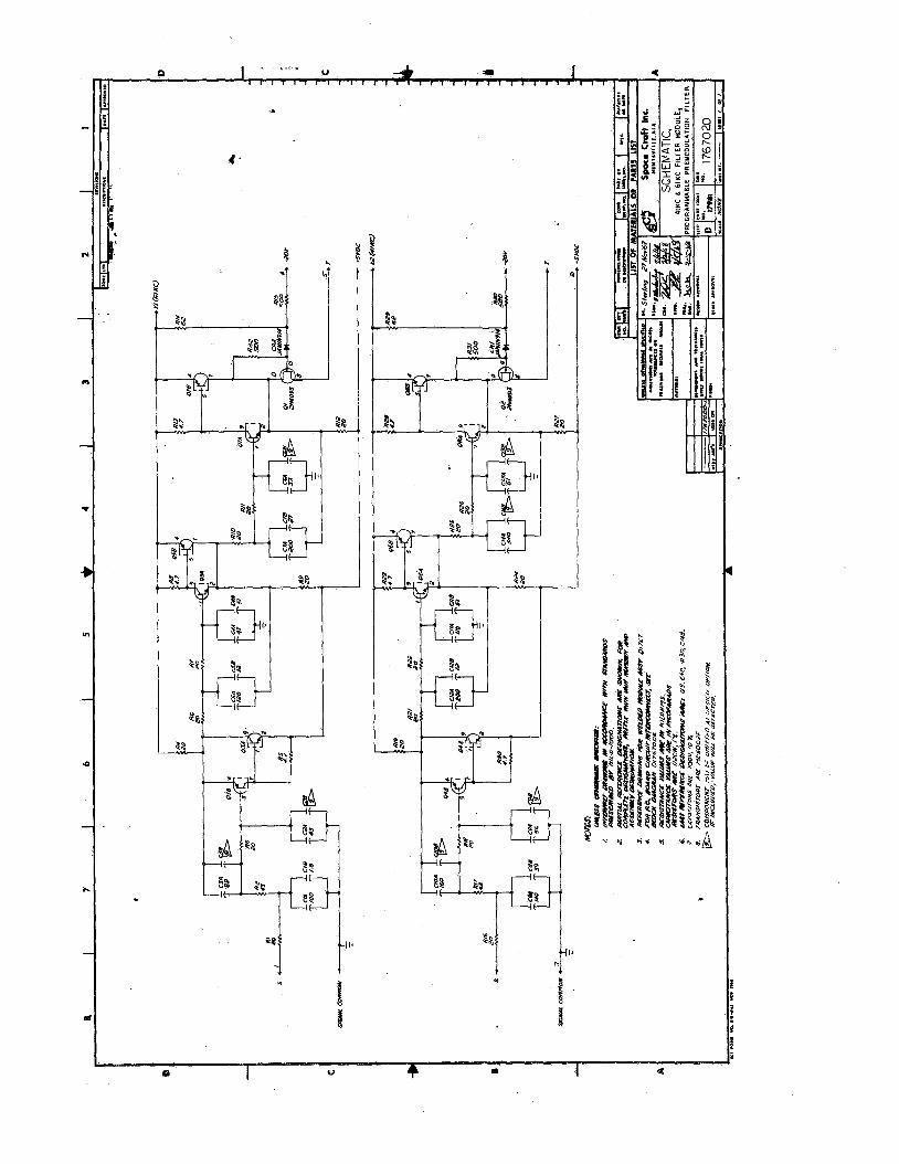
The f i l ters a r e shown in Figures 1767012, 014, 016, 018, 020, 022, and 024.
The fi l ters have low pass characterist ics defined by seventh order Bessel
Polynomials. The Bessel characterist ic gives the best reproduction of the
band pass information, while holding the step response overshoot to a minimum.
The filter consists of three cascaded stages to give the overall character-
ist ic desired.
order sections.
to a seventh order to obtain a fas ter roll-off near the corner frequency and
final attenuation greater than 36 db/octave.
complementary t ransis tors connected for unity gain to minimize the effects of
t ransis tor gain variations and output impedance on the filter Characteristic.
Thef i r s t stage is a third order section, followed by two second
The filter was increased from the sixth order in the proposal
The active elements a r e
The field effect t ransis tor connected in ser ies with the filter output is a
switch which is normally biased trofflt.
a positive twenty volts signal puts that particular filter in operation.
twenty volt filter voltage is supplied by the logic decoding circuits.
field effect t ransis tor connects the filter to the output buffer.
The field effect is turned t'on'' when
The
The
Y) B a

4 c 8
t
(I; i
0 ' I U + P I <

P

L I
t

.
4
YI e s e
I I I

Pa --.rvc
4 B
Output Buff e r
The output buffer is shown in Figure 1767034. The circuit is identical to
the output buffer used on the previous design and included in SCI proposal
P67-116. Output number one produces an output of 3 volts RMS balanced
about ground.
module except for R 9 and R6.
t es t to obtain the desired peak to peak output voltage.
The nominal values of the res i s tors a r e welded into the
The value of Rg and R 6 a r e selected during
The option of selecting
the other res i s tor values was desired in case a m o r e precision adjustment
is necessary. Diode Cr2 compensates for the Vbe temperature drift of Qlb.
Output number two produces unipolar output f rom ground to five volts.
t ransis tors a r e connected for unity gain.
the input divider chain.
for with diode CR 1.
The
The output amplitude is fixed with
The Vbe temperature variations a r e compensated
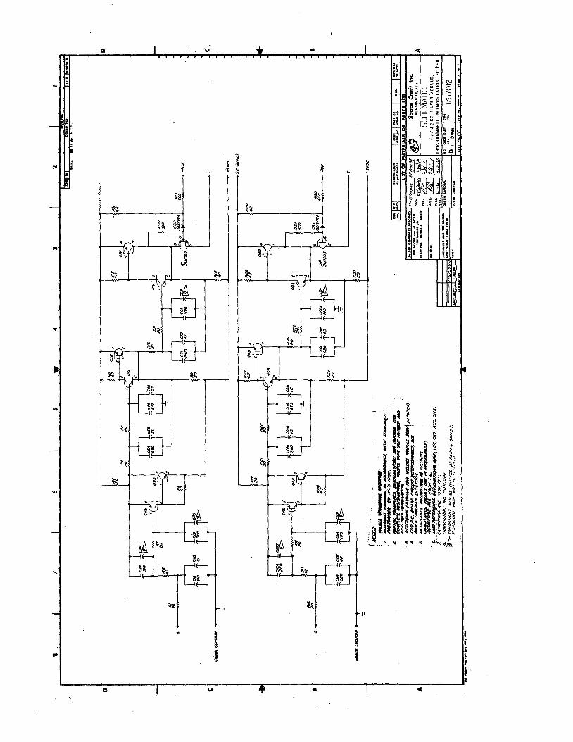
Binary Buffer
The binary buffers a r e shown in figure 1767032.
the logic circuits a t the request of MSC to provide D. C. isolation between the
binary inputs and al l other ground systems.
with the 75K res i s tor in se r i e s with each binary input.
turns tfonft a chopper which A. C. couples a signal to the logic decoding
circuits.
The buffers were added to
The input impedance is guaranteed
The input t ransis tor
The isolated signal is processed to obtain both logic states.
Logic Decoding
The logic decoding shown in figure 1767026 is identical to circuit proposed in
the original proposal P67-116.
Gates sensitive to a l l high level inputs.
with a s e r i e s t ransis tor Qlb .
request of MSC for short circuit protection on the individual filters.
The decoding is accomplished with NAND
The power to the filter is controlled
The resis tor R5 and C1 were added at the
The

1 1 --

ENGINEERING EVA LUA TION UNIT
The engine ering evaluation unit was manufactured to verify the electrical
and mechanical designs. In a high density system with the complexity of
the Programmable Premodulation Fi l ter it is desirable to evaluate a unit
in the packaged configuration before producing flight units. The majority
of corrections and modification involved changes to documentation.
The testing of the evaluation unit revealed severa l desirable modifications
involving the circuit design and layout.
of the printed wiring cable on the signal and power input cable.
r i s e and fall t imes of the signal input were capacitively coupled directly to
the output through the printed wiring cable and the P. C. board track. The
modification requires wiring the connector with shielded cables to the output
pins on the modules.
The major change was the elimination
The fast
This process reduced the pickup to a n acceptable level.
After a l l desirable modifications were made on the evaluation unit the
system performance was evaluated over the required temperature range.
The performance over the temperature range was excellent indicating the
design and modifications were acceptable for the manufacturing of the flight
systems *

h

h

protection has value in that i f a f i l ter developes a short circuit the current
increase will belimited by R5 to a level below the short circuit current of
the power converter, thereby eliminating any possibility of a low voltage
blocking condition occurring.
the voltages dropped to a point that i t was not possible to change from the
affected fi l ter by changing the binary code.
The blocking condition is a possible result i f

MECHANICAL DESIGN
The mechanical design proposed for the Programmable Premodulation
F i l te r was followed in the actual design.
microminature components welded on cordwood modules. The modules a r e
mounted on P. C. boards and placed in an aluminum housing. The P. C.
boards and modules within the housing a r e encapsulated with a thermal
bonding foam to give maximum mechanical strength.
The construction centers around
The only deviation from the proposal i s an increase in volume resulting
from the MSC requirement for D. C, isolation of the binary inputs, The
volume excluding connectors is fifteen (15) cubic inches and weighs
approximately 15 ounces.

TYPE QUALIFICATION TESTING
The Type Qualification Testing was performed by Space Craft , Inc. and
Wyle Laboratories on the first production system.
in accordance with the SCI Q T P 1767, Revision B.
environments provided by Space Craft were the vibration and the five day
temperature cycle.
acceleration, acoustic noise, humidity, sand and dust, altitude, deep space,
thermal vacuum, explosive atmosphere, and salt fog.
The system was tested
The particular
The environments provided by Wyle included shock,
Only two failures occurred during the qualification testing. One failure was
output number two went open circuit while output number one continued to
function normally during the l a s t minutes of the vibration testing. The
fault was found to be the connection of the shielded cable to the r e a r of the
connector.
adhesive.
The connection was repaired and the a r e a ruggedized with an
The documentation was modified to incorporate this addition.
The system was reassembled and subjected to the complete vibration tes t
again at the direction of MSC Quality Control,
the Qualification Unit is approximately three hours.
The total vibration t ime for
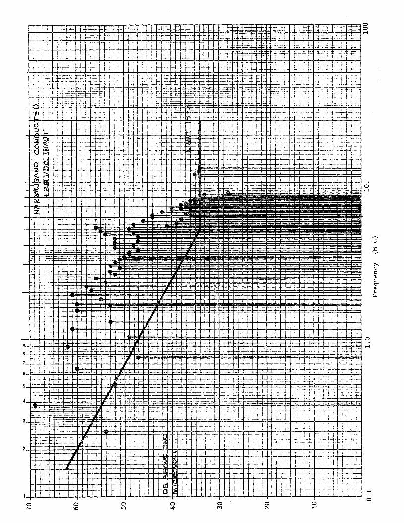
The other failure occurred during the R F I Test.
able l imi t s foa conducted interference of IFSD 19-3. The unit exceed the allow-
A t the direction of
MSC the unit was opened and modified to reduce the conducted interference
to an acceptable level.
The modification consisted of increasing the values of chokes and capacitors
in the power input filter and the addition of a choke in the positive 28 volt
line and a choke in the power return line.
modification a r e enclosed for review.
Test results before and after
n 0
c W
0 r-
0 Ln
0 \D
0 N
0 rl

,
0
0 0--
0- cr)
a
0 cv 0 -
_ I
I
0

. I
!
. . .
. _ . ..-- !
1 . . . I
I . .
.. .. - I
!
. . . 8
.- .
0
. . - 0 ; . - . ... . L
0 cb
.- . . . , . ,
-_
0 z
c . L d

FLIGHT QUALIFICATION
The Flight Qualification Testing was performed on the two flight system.
The Flight Qualification Testing environments included vibration, acceleration,
altitude and a temperature cycle test.
The time required to perform the functional tes t during vibration and
acceleration is approximately one and one half hours for each test.
Space Craft resident authority on environmental testing felt that such test
durations might jeopardize the acceptability of the units a s flight hardware,
Space Craft informed MSC of the length of the present functional tes t and
suggested an abbreviated tes t to reduce the vibration time.
Space Craft to tes t the flight units in accordance with the established
functional test.
The
MSC directed

OPERATING INST RUCTIONS
The Programmable Premodulation Fi l ter power input is applied with
positive twenty-eight (4-28) volts to pin 15 on J1 and power common
connected to pin 16 on J1. The signal input is pin 13 on J1.
signal common is pin 11 on J1.
volts i n amplitude with r i s e and fall t imes of 1.0 microsecond o r less .
The input
The input signal should be 4. 0 volts to 7.0
The output signal is obtained from one o r both output pins.
pin 18 on J1 and output No. 2 is pin 19 on J1 with signal output common on
pin 8 of J1.
Output No. 1 is
The output impedance is l e s s than 1K ohms for each output.
The binary inputs a r e on J2 with provisions for programming the fi l ter with
a voltage provided on Pins 4 and 14 of J2.
Binary two is pin 5 and 15, binary three is pin 3 and 11 and binary four is
pin 6 and 16. To program the filter f rom an external source, connect a
positive three to ten volts to the binary inputs for the desired binary number
and the source common to pin 1, 7 o r 1 9 on J2.
the internal voltage, connect the voltage on pins 4 and 14 to the binary inputs
for the desired binary number.
Binary one is pin 12 and 13,
To program the filter with
The ground systems for the internal voltage and the binary inputs a r e
common, therefore no external connection is required for the ground systems,
The binary numbers and the corresponding cut off bit ra te a r e listed below.

CODE BIT RATE
0000
000 1
00 10
0011
0100
0101
0110
0111
1000
100 1
10 10
1011
1100
1101
1110
1111
No Filter
103 KHZ
94 KHZ
79 KHZ
69 KHZ
61 KHZ
52 KHZ
41 KHZ
31 KHZ
26 KHZ
21 KHZ
11 KHZ
5.2 KHZ
2 . 6 KHZ
1.1 KHZ
No Fil ter
For more detailed procedure to verify performance of the PPF o r to operate
the unit alone, refer to SCI A T P 1767, Revision B.

CONCLUSION
The design and manufacture of the Programmable Premodulation Filter
proceeded w i t h relatively few problems.
Premodulation Filter P rogram was employed on the Programmable Pre-
modulation Filter P rogram with no changes in the design philosophy.
programming capability is a n addition to the past requirements,
performance w a s satisfactory wi th only a few component value changes to
improve the high frequency response.
the fi l ter sections to provide a sharper roll-off past the corner frequency
which was a change f rom a sixth order fi l ter to a seventh order filter.
The basic design of the previous
The
The circuit
An improvement w a s incorporated into
The successful completion of the qualification testing allows significant confi-
dence in the circuit design and reliability of the Programmable Premodulation
Fil ter under all environments. The basic approach to active filter design as
used by SCI of calculating component ra t ios to set filter Q values as opposed
to the more common feedback gain adjustment is considered w e l l proven and
the stability exhibited by these filters over the long tes t period w a s considered
ve ry satisfactory,
The qualification testing required significantly more test time than w a s
originally anticipated for the contract.
length of the functional test.
filter performance with a 10% duty cycle square wave. A sinusoidal tes t
would be easier and quicker to perform but is not possible with the square
The lengthy test t ime w a s due to the
This in turn w a s due to some extent to checking
wave buffer input.
point should be considered which would allow sinusoidal checking of the f i l ters
af ter the buffer, with a separate buffer check,
In the event of fur ther or similar development a tes t

The 10% duty cycle test duration for vibration and acceleration is more than
fifteen t imes grea te r than the test times in the original specification, which
might suggest that the acceptability of the flight units for "flight hardware"
could be jeopardized.
verify the unit performance without jeopardizing the "flight hardware".
the adoption of a sinusoidal test as suggested would simplify the problem.
An abbreviated test could reduce the tes t time and still
Also
Outside finish on the case survived the environmental test very w e l l with some
minor pitting in the plate after the salt fog test.
handling had occurred in previous tests and the scratches in the plate a r e
considered to be the cause of the pitting,
Some scratching due to
Of the connectors used one w a s gold plated and the other tin plated.
plate w a s more affected by the environments than the gold plate,,
was used on al l flight unit connectors.
The t in
Gold plate
The manufacturing processes involved in the unit w e r e standard SCI processes
and no manufacturing problems encountered.
of the design and tes t programs the design of the unit meets all of the specifi-
cation requirements and it is a manufacturable unit.
It is concluded that a s a result